Embed Size (px)
Citation preview

1. General description
The SA616 is a low-voltage high performance monolithic FM IF system incorporating a mixer/oscillator, two limiting intermediate frequency amplifiers, quadrature detector, logarithmic Received Signal Strength Indicator (RSSI), voltage regulator and audio and RSSI op amps. The SA616 is available in SSOP20 and HVQFN20 packages.
The SA616 was designed for portable communication applications and will function down to 2.7 V. The RF section is similar to the famous SA615. The audio and RSSI outputs have amplifiers with access to the feedback path. This enables the designer to adjust the output levels or add filtering.
2. Features and benefits
Low power consumption: 3.5 mA typical at 3 V
Mixer input to >150 MHz
Mixer conversion power gain of 17 dB at 45 MHz
XTAL oscillator effective to 150 MHz (LC oscillator or external oscillator can be used at higher frequencies)
102 dB of IF amp/limiter gain
2 MHz IF amp/limiter small signal bandwidth
Temperature compensated logarithmic RSSI with a 80 dB dynamic range
Low external component count; suitable for crystal/ceramic/LC filters
Excellent sensitivity: 0.31 V into 50 matching network for 12 dB SINAD (Signal-to-Noise-and-Distortion ratio) for 1 kHz tone with RF at 45 MHz and IF at 455 kHz
SA616 meets cellular radio specifications
Audio output internal op amp
RSSI output internal op amp
Internal op amps with rail-to-rail outputs
ESD protection exceeds 2000 V HBM per JESD22-A114 and 1000 V CDM per JESD22-C101
Latch-up testing is done to JEDEC Standard JESD78 Class II, Level B
3. Applications
Portable cellular radio FM IF
Cordless phones
Wireless systems
RF level meter
SA616Low-voltage high performance mixer FM IF systemRev. 5 — 24 July 2012 Product data sheet

NXP Semiconductors SA616Low-voltage high performance mixer FM IF system
Spectrum analyzer
Instrumentation
FSK and ASK data receivers
Log amps
Portable high performance communication receiver
Single conversion VHF receivers
4. Ordering information
5. Block diagram
Table 1. Ordering informationTamb = 40 C to +85 C
Type number Topside mark
Package
Name Description Version
SA616DK/01 SA616DK SSOP20 plastic shrink small outline package; 20 leads; body width 4.4 mm
SOT266-1
SA616BS 616B HVQFN20 plastic thermal enhanced very thin quad flat package; no leads; 20 terminals; body 4 4 0.85 mm
SOT917-1
Pin numbers for SSOP20; HVQFN20 pins shown in parentheses.
Fig 1. Block diagram of SA616
002aaf352
mixer
IF amplimiter
OSC RSSI
quad
audio
VREG
E B
20(18)
19(17)
18(16)
17(15)
16(14)
15(13)
14(12)
13(11)
12(10)
11(9)
1(19)
2(20)
3(1)
4(2)
5(3)
6(4)
7(5)
8(6)
9(7)
10(8)
SA616 All information provided in this document is subject to legal disclaimers. © NXP B.V. 2012. All rights reserved.
Product data sheet Rev. 5 — 24 July 2012 2 of 31
NXP Semiconductors SA616Low-voltage high performance mixer FM IF system
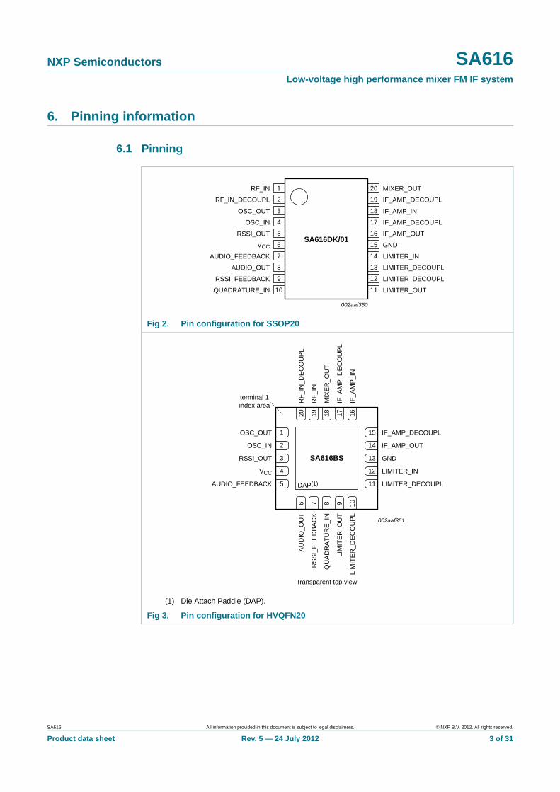
6. Pinning information
6.1 Pinning
Fig 2. Pin configuration for SSOP20
(1) Die Attach Paddle (DAP).
Fig 3. Pin configuration for HVQFN20
SA616DK/01
RF_IN MIXER_OUT
RF_IN_DECOUPL IF_AMP_DECOUPL
OSC_OUT IF_AMP_IN
OSC_IN IF_AMP_DECOUPL
RSSI_OUT IF_AMP_OUT
VCC GND
AUDIO_FEEDBACK LIMITER_IN
AUDIO_OUT LIMITER_DECOUPL
RSSI_FEEDBACK LIMITER_DECOUPL
QUADRATURE_IN LIMITER_OUT
002aaf350
1
2
3
4
5
6
7
8
9
10
12
11
14
13
16
15
18
17
20
19
002aaf351
SA616BS
Transparent top view
LIMITER_DECOUPL
VCC
AUDIO_FEEDBACK
LIMITER_IN
RSSI_OUT GND
OSC_IN IF_AMP_OUT
OSC_OUT IF_AMP_DECOUPL
AU
DIO
_OU
T
RS
SI_
FE
ED
BA
CK
QU
AD
RA
TU
RE
_IN
LIM
ITE
R_O
UT
LIM
ITE
R_D
EC
OU
PL
RF
_IN
_DE
CO
UP
L
RF
_IN
MIX
ER
_OU
T
IF_A
MP
_DE
CO
UP
L
IF_A
MP
_IN
5 11
4 12
3 13
2 14
1 15
6 7 8 9 10
20 19 18 17 16
terminal 1index area
DAP(1)
SA616 All information provided in this document is subject to legal disclaimers. © NXP B.V. 2012. All rights reserved.
Product data sheet Rev. 5 — 24 July 2012 3 of 31

NXP Semiconductors SA616Low-voltage high performance mixer FM IF system
6.2 Pin description
[1] HVQFN20 package supply ground is connected to both GND pin and exposed center pad. GND pin must be connected to supply ground for proper device operation. For enhanced thermal, electrical, and board level performance, the exposed pad needs to be soldered to the board using a corresponding thermal pad on the board and for proper heat conduction through the board, thermal vias need to be incorporated in the PCB in the thermal pad region.
Table 2. Pin description
Symbol Pin Description
SSOP20 HVQFN20
RF_IN 1 19 RF input
RF_IN_DECOUPL 2 20 RF input decoupling pin
OSC_OUT 3 1 oscillator output
OSC_IN 4 2 oscillator input
RSSI_OUT 5 3 RSSI output
VCC 6 4 positive supply voltage
AUDIO_FEEDBACK 7 5 audio amplifier negative feedback terminal
AUDIO_OUT 8 6 audio amplifier output
RSSI_FEEDBACK 9 7 RSSI amplifier negative feedback terminal
QUADRATURE_IN 10 8 quadrature detector input terminal
LIMITER_OUT 11 9 limiter amplifier output
LIMITER_DECOUPL 12 10 limiter amplifier decoupling pin
LIMITER_DECOUPL 13 11 limiter amplifier decoupling pin
LIMITER_IN 14 12 limiter amplifier input
GND 15 13[1] ground; negative supply
IF_AMP_OUT 16 14 IF amplifier output
IF_AMP_DECOUPL 17 15 IF amplifier decoupling pin
IF_AMP_IN 18 16 IF amplifier input
IF_AMP_DECOUPL 19 17 IF amplifier decoupling pin
MIXER_OUT 20 18 mixer output
- - DAP exposed die attach paddle
SA616 All information provided in this document is subject to legal disclaimers. © NXP B.V. 2012. All rights reserved.
Product data sheet Rev. 5 — 24 July 2012 4 of 31

NXP Semiconductors SA616Low-voltage high performance mixer FM IF system
7. Functional description
The SA616 is an IF signal processing system suitable for second IF systems with input frequency as high as 150 MHz. The bandwidth of the IF amplifier and limiter is at least 2 MHz with 90 dB of gain. The gain/bandwidth distribution is optimized for 455 kHz, 1.5 k source applications. The overall system is well-suited to battery operation as well as high performance and high quality products of all types.
The input stage is a Gilbert cell mixer with oscillator. Typical mixer characteristics include a noise figure of 6.2 dB, conversion gain of 17 dB, and input third-order intercept of 9 dBm. The oscillator will operate in excess of 200 MHz in L/C tank configurations. Hartley or Colpitts circuits can be used up to 100 MHz for crystal configurations. Butler oscillators are recommended for crystal configurations up to 150 MHz.
The output impedance of the mixer is a 1.5 k resistor permitting direct connection to a 455 kHz ceramic filter. The input resistance of the limiting IF amplifiers is also 1.5 k. With most 455 kHz ceramic filters and many crystal filters, no impedance matching network is necessary. The IF amplifier has 43 dB of gain and 5.5 MHz bandwidth. The IF limiter has 60 dB of gain and 4.5 MHz bandwidth.
To achieve optimum linearity of the log signal strength indicator, there must be a 12 dBV insertion loss between the first and second IF stages. If the IF filter or interstage network does not cause 12 dBV insertion loss, a fixed or variable resistor or an L pad for simultaneous loss and impedance matching can be added between the first IF output (IF_AMP_OUT) and the interstage network. The overall gain will then be 90 dB with 2 MHz bandwidth.
The signal from the second limiting amplifier goes to a Gilbert cell quadrature detector. One port of the Gilbert cell is internally driven by the IF. The other output of the IF is AC-coupled to a tuned quadrature network. This signal, which now has a 90 phase relationship to the internal signal, drives the other port of the multiplier cell.
The demodulated output of the quadrature drives an internal op amp. This op amp can be configured as a unity gain buffer, or for simultaneous gain, filtering, and second-order temperature compensation if needed. It can drive an AC load as low as 5 k with a rail-to-rail output.
A log signal strength completes the circuitry. The output range is greater than 90 dB and is temperature compensated. This log signal strength indicator exceeds the criteria for AMPS or TACS cellular telephone. This signal drives an internal op amp. The op amp is capable of rail-to-rail output. It can be used for gain, filtering, or second-order temperature compensation of the RSSI, if needed.
Remark: dBV = 20log VO/VI.
SA616 All information provided in this document is subject to legal disclaimers. © NXP B.V. 2012. All rights reserved.
Product data sheet Rev. 5 — 24 July 2012 5 of 31

NXP Semiconductors SA616Low-voltage high performance mixer FM IF system
8. Limiting values
9. Thermal characteristics
10. Static characteristics
Table 3. Limiting valuesIn accordance with the Absolute Maximum Rating System (IEC 60134).
Symbol Parameter Conditions Min Max Unit
VCC supply voltage - 7 V
Tstg storage temperature 65 +150 C
Tamb ambient temperature operating 40 +85 C
Table 4. Thermal characteristics
Symbol Parameter Conditions Max Unit
Zth(j-a) transient thermal impedance from junction to ambient
SA616DK/01 (SSOP20) 117 K/W
SA616BS (HVQFN20) 40 K/W
Table 5. Static characteristicsVCC = 3 V; Tamb = 25 C; unless specified otherwise.
Symbol Parameter Conditions Min Typ Max Unit
VCC supply voltage 2.7 - 7.0 V
ICC supply current - 3.5 5.0 mA
SA616 All information provided in this document is subject to legal disclaimers. © NXP B.V. 2012. All rights reserved.
Product data sheet Rev. 5 — 24 July 2012 6 of 31

NXP Semiconductors SA616Low-voltage high performance mixer FM IF system
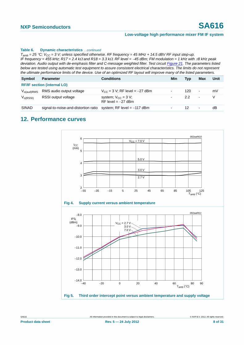
11. Dynamic characteristics
Table 6. Dynamic characteristicsTamb = 25 C; VCC = 3 V; unless specified otherwise. RF frequency = 45 MHz + 14.5 dBV RF input step-up. IF frequency = 455 kHz; R17 = 2.4 k and R18 = 3.3 k. RF level = 45 dBm; FM modulation = 1 kHz with 8 kHz peak deviation. Audio output with de-emphasis filter and C-message weighted filter. Test circuit Figure 21. The parameters listed below are tested using automatic test equipment to assure consistent electrical characteristics. The limits do not represent the ultimate performance limits of the device. Use of an optimized RF layout will improve many of the listed parameters.
Symbol Parameter Conditions Min Typ Max Unit
Mixer/oscillator section (external LO = 220 mV RMS value)
fi input frequency - 150 - MHz
fosc oscillator frequency - 150 - MHz
NF noise figure at 45 MHz - 6.8 - dB
IP3I input third-order intercept point 50 source; f1 = 45.0 MHz; f2 = 45.06 MHz; input RF level = 52 dBm
- 9 - dB
Gp(conv) conversion power gain matched 14.5 dBV step-up 11 17 - dB
50 source - 2.5 - dB
Ri(RF) RF input resistance single-ended input - 8 - k
Ci(RF) RF input capacitance - 3.0 4.0 pF
Ro(mix) mixer output resistance MIXER_OUT pin 1.25 1.5 - k
IF section
Gamp(IF) IF amplifier gain 50 source - 44 - dB
Glim limiter gain 50 source - 58 - dB
Pi(IF) IF input power for 3 dB input limiting sensitivity; R17 = 2.4 k; R18 = 3.3 k (Figure 21); test at IF_AMP_IN pin
- 105 - dBm
AM AM rejection 80 % AM 1 kHz - 40 - dB
Vo(aud) audio output voltage gain of two (2 k AC load) 60 120 - mV
SINAD signal-to-noise-and-distortion ratio IF level 110 dBm - 17 - dB
THD total harmonic distortion 30 45 - dB
S/N signal-to-noise ratio no modulation for noise - 62 - dB
Vo(RSSI) RSSI output voltage RF; R9 = 2 k
RF level = 118 dBm - 0.3 0.8 V
RF level = 68 dBm 0.7 1.1 2 V
RF level = 23 dBm 1.0 1.8 2.5 V
RSSI(range) RSSI range - 80 - dB
RSSI RSSI variation - 2 - dB
Zi(IF) IF input impedance IF_AMP_IN pin 1.3 1.5 - k
Zo(IF) IF output impedance IF_AMP_OUT pin - 0.3 - k
Zi(lim) limiter input impedance LIMITER_IN pin 1.3 1.5 - k
Zo(lim) limiter output impedance LIMITER_OUT pin - 0.3 - k
Vo(RMS) RMS output voltage LIMITER_OUT pin - 130 - mV
SA616 All information provided in this document is subject to legal disclaimers. © NXP B.V. 2012. All rights reserved.
Product data sheet Rev. 5 — 24 July 2012 7 of 31
NXP Semiconductors SA616Low-voltage high performance mixer FM IF system
12. Performance curves
RF/IF section (internal LO)
Vo(aud)RMS RMS audio output voltage VCC = 3 V; RF level = 27 dBm - 120 - mV
Vo(RSSI) RSSI output voltage system; VCC = 3 V; RF level = 27 dBm
- 2.2 - V
SINAD signal-to-noise-and-distortion ratio system; RF level = 117 dBm - 12 - dB
Table 6. Dynamic characteristics …continuedTamb = 25 C; VCC = 3 V; unless specified otherwise. RF frequency = 45 MHz + 14.5 dBV RF input step-up. IF frequency = 455 kHz; R17 = 2.4 k and R18 = 3.3 k. RF level = 45 dBm; FM modulation = 1 kHz with 8 kHz peak deviation. Audio output with de-emphasis filter and C-message weighted filter. Test circuit Figure 21. The parameters listed below are tested using automatic test equipment to assure consistent electrical characteristics. The limits do not represent the ultimate performance limits of the device. Use of an optimized RF layout will improve many of the listed parameters.
Symbol Parameter Conditions Min Typ Max Unit
Fig 4. Supply current versus ambient temperature
Fig 5. Third order intercept point versus ambient temperature and supply voltage
Tamb (°C)−55 1255
002aaf410
4
6
ICC(mA)
265 105854525−15−35
VCC = 7.0 V
5.0 V
3.0 V
2.7 V3
5
Tamb (°C)−40 9060−20
002aaf411
−11.0
−9.0
−8.0IP3I
(dBm)
−14.00 20 40 80
−10.0
−12.0
−13.0
VCC = 2.7 V3.0 V7.0 V
SA616 All information provided in this document is subject to legal disclaimers. © NXP B.V. 2012. All rights reserved.
Product data sheet Rev. 5 — 24 July 2012 8 of 31

NXP Semiconductors SA616Low-voltage high performance mixer FM IF system
Fig 6. Mixer noise figure versus ambient temperature and supply voltage
Fig 7. Conversion gain versus ambient temperature and supply voltage
Tamb (°C)−40 9060−20
002aaf412
6.5
7.5
8.0NF
(dB)
5.00 20 40 80
7.0
6.0
5.5
VCC = 2.7 V3.0 V7.0 V
Tamb (°C)−40 9060−20
002aaf413
17.0
16.5
17.5
18.0
Gp(conv)(dB)
16.00 20 40 80
VCC = 2.7 V3.0 V7.0 V
SA616 All information provided in this document is subject to legal disclaimers. © NXP B.V. 2012. All rights reserved.
Product data sheet Rev. 5 — 24 July 2012 9 of 31

NXP Semiconductors SA616Low-voltage high performance mixer FM IF system
RF = 45 MHz; IF = 455 kHz.
(1) Fund product.
(2) Third order product.
(3) 50 input.
Fig 8. Mixer third order intercept and compression
RF(3) input level (dBm)−66 3414−26 −6−46
002aaf414
−40
−20
−60
0
20
IF output power(dBm)
−80
(1) (2)
SA616 All information provided in this document is subject to legal disclaimers. © NXP B.V. 2012. All rights reserved.
Product data sheet Rev. 5 — 24 July 2012 10 of 31

NXP Semiconductors SA616Low-voltage high performance mixer FM IF system
VCC = 3 V; RF = 45 MHz; deviation = 8 kHz; Vo(aud)RMS = 104.9 mV.
Fig 9. Relative level of audio, AM rejection, THD+N and noise versus RF level (Tamb = 40 C)
VCC = 3 V; RF = 45 MHz; deviation = 8 kHz; Vo(aud)RMS = 117.6 mV.
Fig 10. Relative level of audio, AM rejection, THD+N and noise versus RF level (Tamb = +25 C)
002aaf415
−55
−45
−35
−25
−5
RF level (dBm)−125 −25−45−85 −65−105
audio
noise
THD+N
AM rejection
−15
5relative level
(dB)
−65
002aaf416
−15
5
−65
−55
−45
−35
−25
−5
RF level (dBm)−125 −25−45−85 −65−105
audio
noise
THD+N
AM rejection
relative level(dB)
SA616 All information provided in this document is subject to legal disclaimers. © NXP B.V. 2012. All rights reserved.
Product data sheet Rev. 5 — 24 July 2012 11 of 31

NXP Semiconductors SA616Low-voltage high performance mixer FM IF system
VCC = 3 V; RF = 45 MHz; deviation = 8 kHz; Vo(aud)RMS = 127 mV.
Fig 11. Relative level of audio, AM rejection, THD+N and noise versus RF level (Tamb = +85 C)
VCC = 3 V; RF = 45 MHz; RF level = 45 dBm; deviation = 8 kHz; Vo(aud)RMS = +117.6 mV.
Fig 12. Relative audio level, distortion, AM rejection and noise versus ambient temperature
002aaf417
−15
5
−65
−55
−45
−35
−25
−5
RF level (dBm)−125 −25−45−85 −65−105
audio
noise
THD+N
AM rejection
relative level(dB)
Tamb (°C)−55 125655−35
002aaf418
−15
5
−65−15 20 45 85 105
−55
−45
−35
−25
−5
audio
noise
distortion
AM rejection
relative level(dB)
SA616 All information provided in this document is subject to legal disclaimers. © NXP B.V. 2012. All rights reserved.
Product data sheet Rev. 5 — 24 July 2012 12 of 31

NXP Semiconductors SA616Low-voltage high performance mixer FM IF system
455 kHz IF at 3 V.
Fig 13. RSSI output voltage versus IF level
VCC = 3 V
Fig 14. RSSI output voltage versus RF level
IF level (dBm)−95 5−15−55 −35−75
002aaf419
0.8
1.6
2.4Vo(RSSI)
(V)
0
0.4
1.2
2.0Tamb = +85 °C
room−40 °C
RF level (dBm)−125 −25−45−85 −65−105
002aaf420
0.9
1.5
2.1Vo(RSSI)
(V)
0.3
0.6
1.2
1.8
Tamb = +85 °C+27 °C−40 °C
SA616 All information provided in this document is subject to legal disclaimers. © NXP B.V. 2012. All rights reserved.
Product data sheet Rev. 5 — 24 July 2012 13 of 31

NXP Semiconductors SA616Low-voltage high performance mixer FM IF system
13. Application information
Fig 15. RMS audio output voltage versus ambient temperature
Tamb (°C)−55 1255
002aaf421
65 105854525−15−35
VCC = 7.0 V
5.0 V
3.0 V
2.7 V100
200
300
Vo(aud)RMS(mV)
0
The layout is very critical in the performance of the receiver. We highly recommend our demo board layout.
All of the inductors, the quad tank, and their shield must be grounded. A 10 F to 15 F or higher value tantalum capacitor on the supply line is essential. A low frequency ESR screening test on this capacitor will ensure consistent good sensitivity in production. A 0.1 F bypass capacitor on the supply pin, and grounded near the 44.545 MHz oscillator improves sensitivity by 2 dB to 3 dB.
Fig 16. SA616 45 MHz application circuit (SA616DK demo board)
002aaf408
mixer
IF amplimiter
OSC RSSI
quad
audio
VREG
20 19 18 17 16 15 14 13 12 11
1 2 3 4 5 6 7 8 9 10
C23 C21FL1
C18 C17FL2
R17
2.4 kΩ
R183.3 kΩ
C26
C15
C9
C10
VCCRSSI_OUT
R11
10 kΩC12R10
8.2 kΩ
AUDIO_OUT
C27 R1911 kΩ
IFT1
C19390 pF C14
C7
L2
X1
C6
C8
C5
L1
C1
C2
45 MHzinput
SA616 All information provided in this document is subject to legal disclaimers. © NXP B.V. 2012. All rights reserved.
Product data sheet Rev. 5 — 24 July 2012 14 of 31

NXP Semiconductors SA616Low-voltage high performance mixer FM IF system
[1] This is a 30 kHz bandwidth 455 kHz ceramic filter. Al the characterization and testing are done with this wideband filter. A more narrowband 15 kHz bandwidth 455 kHz ceramic filter that may be used as an alternative selection is Murata CFUKG455KE4A-R0.
[2] R5 can be used to bias the oscillator transistor at a higher current for operation above 45 MHz. Recommended value is 22 k, but should not be below 10 k.
Table 7. SA616DK demo board component list
Component Description
C1 51 pF NPO ceramic
C2 220 pF NPO ceramic
C5, C9, C14, C17, C18, C21, C23, C26
100 nF 10 % monolithic ceramic
C6 30 pF trim cap
C7 1 nF ceramic
C8, C15 10.0 pF NPO ceramic
C10 15 F tantalum (minimum)
C12 2.2 F 10 % tantalum
C19 390 pF 10 % monolithic ceramic
C27 2.2 F tantalum
FL1, FL2[1] ceramic filter Murata CFUKF455KB4X-R0
IFT1 330 H Toko 836AN-0129Z
L1 0.33 H Toko A638AN-0158Z
L2 1.2 H Toko FSLM2520-1R2K
X1 44.545 MHz crystal ICM4712701
R5[2] not used in application board
R10 8.2 k 5 % 1/4W carbon composition
R11 10 k 5 % 1/4W carbon composition
R17 2.4 k 5 % 1/4W carbon composition
R18 3.3 k 5 % 1/4W carbon composition
R19 11 k 5 % 1/4W carbon composition
SA616 All information provided in this document is subject to legal disclaimers. © NXP B.V. 2012. All rights reserved.
Product data sheet Rev. 5 — 24 July 2012 15 of 31

NXP Semiconductors SA616Low-voltage high performance mixer FM IF system
Fig 17. SA6x6DK/SA58640DK top view with components
001aal912
TOKO
SA6x6DK SA58640DK
L1
L2
C6
C10
FT1
C9
C27
C12
4.7 nF
RSSI
VCC
AUDIO
GND
AUDIO_DC
IF = 455 kHzRF IN45 MHz
820 Ω
C1 C2C21
C23
C7
X1
44.545 MHz
C8
C5
R11
C15
C14
C17 C18
R19
R17
FIL1
455 kHz
455 kHz
FIL2
R18 C26
C19
R10
U1
SA616 All information provided in this document is subject to legal disclaimers. © NXP B.V. 2012. All rights reserved.
Product data sheet Rev. 5 — 24 July 2012 16 of 31
NXP Semiconductors SA616Low-voltage high performance mixer FM IF system
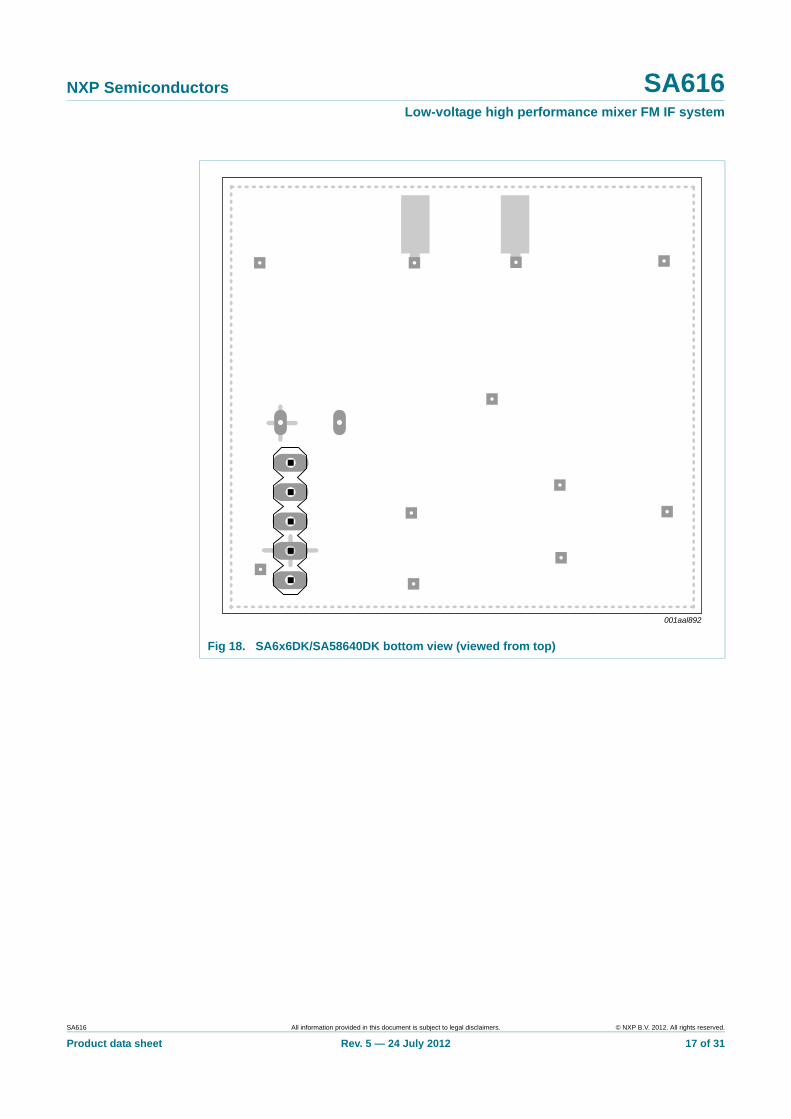
Fig 18. SA6x6DK/SA58640DK bottom view (viewed from top)
001aal892
SA616 All information provided in this document is subject to legal disclaimers. © NXP B.V. 2012. All rights reserved.
Product data sheet Rev. 5 — 24 July 2012 17 of 31
NXP Semiconductors SA616Low-voltage high performance mixer FM IF system
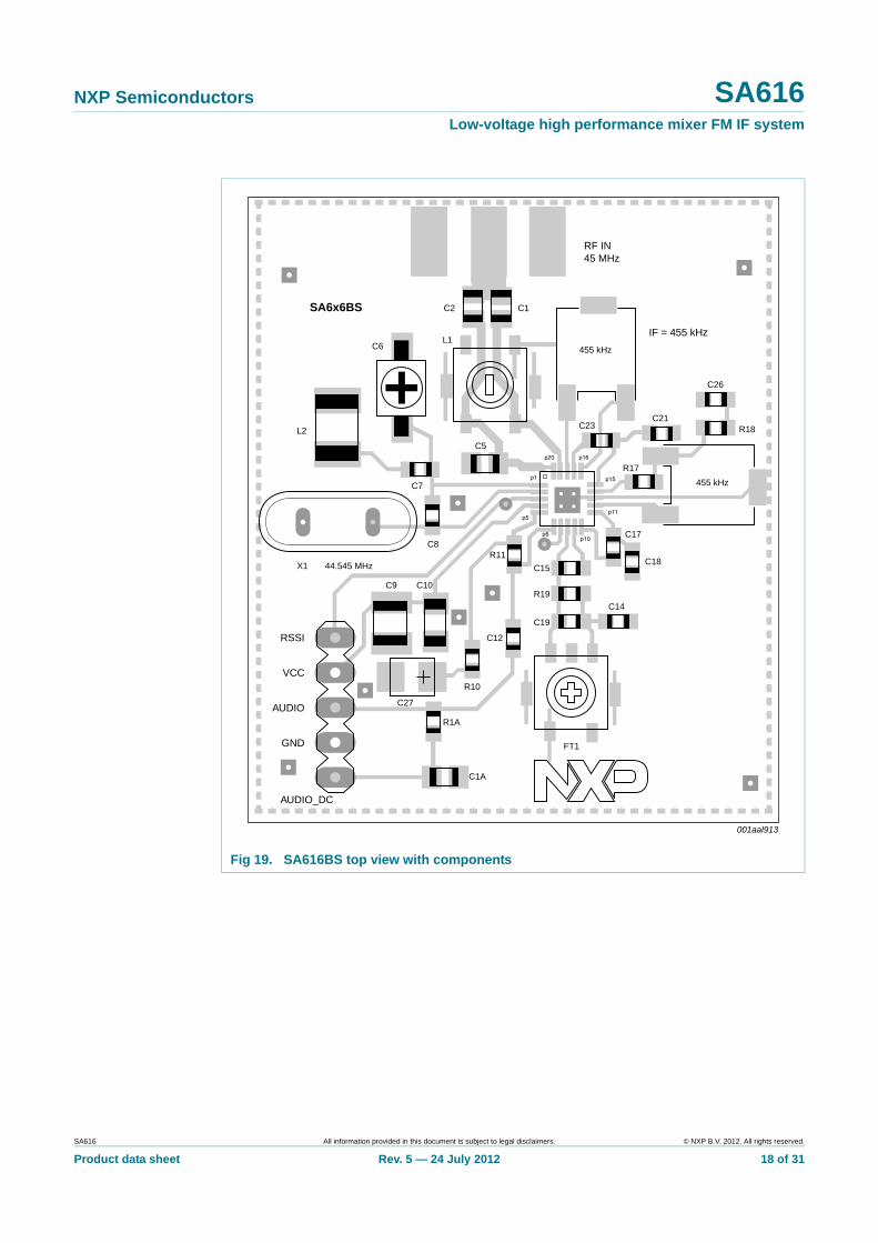
Fig 19. SA616BS top view with components
001aal913
SA6x6BS
RF IN45 MHz
IF = 455 kHz
RSSI
X1
C9 C10
C27
R1A
C1A
FT1
R10
C19
C7
C8
C5
C6L1
L2
C1C2
C26
C21
455 kHz
455 kHz
C23 R18
R17
C14
C18
C17
R19
C15
C12
R1144.545 MHz
VCC
AUDIO
GND
AUDIO_DC
SA616 All information provided in this document is subject to legal disclaimers. © NXP B.V. 2012. All rights reserved.
Product data sheet Rev. 5 — 24 July 2012 18 of 31

NXP Semiconductors SA616Low-voltage high performance mixer FM IF system
Fig 20. SA616BS bottom view (viewed from top)
001aal893
SA616 All information provided in this document is subject to legal disclaimers. © NXP B.V. 2012. All rights reserved.
Product data sheet Rev. 5 — 24 July 2012 19 of 31

NXP Semiconductors SA616Low-voltage high performance mixer FM IF system
14. Test information
Fig 21. SA616 45 MHz test circuit (relays as shown)
002aaf407
mixer
IF amplimiter
OSC RSSI
quad
audio
VREG
20 19 18 17 16 15 14 13 12 11
1 2 3 4 5 6 7 8 9 10
C23 C21FL1 C18 C17FL2
R172.4 kΩ
C26
C15
C9
C10
VCC
RSSI_OUT
C12
R10
AUDIO_OUT
C27 R1916 kΩ
IFT1
C14
C7
L2
X1
C6
C8
L1
C1
C2
45 MHz
C16
1.3 kΩ
51.7 Ω
−36 dB,156 kΩ/50 Ω pad
SW5SW6
C19
32.8 Ω71.5 Ω
96.5 Ω
−10.6 dB,50 Ω/50 Ω pad
SW7
R183.3 kΩ
C20
51.5 Ω
−29 dB,929 Ω/50 Ω pad
SW8
C22
32.6 Ω
96.5 Ω
−10.6 dB,50 Ω/50 Ω pad
71.5 Ω
C24
3880 Ω
50.5 Ω
−25 dB,1500 Ω/50 Ω pad
2430 Ω
SW9
R13
SW11R14
R11
SW10
R12
DEEMPHASISFILTER
R9SW4
R839.2 Ω
R730.5 Ω
R6178 Ω
ext.LOC osc
44.545 MHz
SW3
C5
SW1
R4
C4
51.1
Ω
SW2
C3
R2
R1
R3C-WEIGHTED
AUDIOMEASUREMENT
CIRCUIT
mini-circuitZSC2-1B
45.06MHz
SA616 All information provided in this document is subject to legal disclaimers. © NXP B.V. 2012. All rights reserved.
Product data sheet Rev. 5 — 24 July 2012 20 of 31

NXP Semiconductors SA616Low-voltage high performance mixer FM IF system
[1] This is a 30 kHz bandwidth 455 kHz ceramic filter. Al the characterization and testing are done with this wideband filter. A more narrowband 15 kHz bandwidth 455 kHz ceramic filter that may be used as an alternative selection is Murata CFUKG455KE4A-R0.
Table 8. Automatic test circuit component list
Component Description
C1 100 pF NPO ceramic
C2 390 pF NPO ceramic
C5, C9, C14, C17, C18, C21, C23, C25, C26, C27
100 nF 10 % monolithic ceramic
C6 22 pF NPO ceramic
C7 1 nF ceramic
C8, C15 10 pF NPO ceramic
C10 15 F tantalum (minimum)
C12 2.2 F
FL1, FL2[1] ceramic filter Murata CFUKF455KB4X-R0
IFT1 455 kHz (Ce = 180 pF) Toko RMC-2A6597H
L1 147 nH to 160 nH Coilcraft UNI-10/142-04J08S
L2 0.8 H nominal; Toko 292CNS-T1038Z
R9 2 k 1 % 1/4 W metal film
R10 8.2 k 1 %
R11, R14 10 k 1 %
R12 2 k 1 %
R13 20 k 1 %
R17 2.4 k 5 % 1/4 W carbon composition
R18 3.3 k
R19 16 k
X1 44.545 MHz crystal ICM4712701
SA616 All information provided in this document is subject to legal disclaimers. © NXP B.V. 2012. All rights reserved.
Product data sheet Rev. 5 — 24 July 2012 21 of 31

NXP Semiconductors SA616Low-voltage high performance mixer FM IF system
(1) Set RF generator at 45.000 MHz; use a 1 kHz modulation frequency and a 6 kHz deviation if using 16 kHz filters, or 8 kHz if using 30 kHz filters.
(2) The smallest RSSI voltage (i.e., when no RF input is present and the input is terminated) is a measure of the quality of the layout and design. If the lowest RSSI voltage is 500 mV or higher, it means the receiver is in regenerative mode. In that case, the receiver sensitivity will be worse than expected.
(3) The C-message and de-emphasis filter combination has a peak gain of 10 dB for accurate measurements. Without the gain, the measurements may be affected by the noise of the scope and HP339 analyzer. The de-emphasis filter has a fixed 6 dB/octave slope between 300 Hz and 3 kHz.
Fig 22. SA616 application circuit test setup
SCOPE
SA616 DEMOBOARD(2)
RSSI AUDIO
002aaf409
RF GENERATOR(1)
45 MHz
VCC (+3 V)
DC VOLTMETER
HP339A DISTORTIONANALYZER
C–MESSAGE(3)
DE-EMPHASISFILTER
SA616 All information provided in this document is subject to legal disclaimers. © NXP B.V. 2012. All rights reserved.
Product data sheet Rev. 5 — 24 July 2012 22 of 31
NXP Semiconductors SA616Low-voltage high performance mixer FM IF system
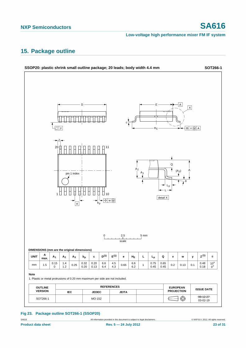
15. Package outline
Fig 23. Package outline SOT266-1 (SSOP20)
UNIT A1 A2 A3 bp c D(1) E(1) (1)e HE L Lp Q Zywv θ
REFERENCESOUTLINEVERSION
EUROPEANPROJECTION ISSUE DATE
IEC JEDEC JEITA
mm 0.150
1.41.2
0.320.20
0.200.13
6.66.4
4.54.3
0.65 1 0.26.66.2
0.650.45
0.480.18
100
o
o0.13 0.1
DIMENSIONS (mm are the original dimensions)
Note
1. Plastic or metal protrusions of 0.20 mm maximum per side are not included.
0.750.45
SOT266-1 MO-15299-12-2703-02-19
w M
θ
AA1
A2
bp
D
HE
Lp
Q
detail X
E
Z
e
c
L
v M A
X
(A )3
A
y
0.25
1 10
20 11
pin 1 index
0 2.5 5 mm
scale
SSOP20: plastic shrink small outline package; 20 leads; body width 4.4 mm SOT266-1
Amax.
1.5
SA616 All information provided in this document is subject to legal disclaimers. © NXP B.V. 2012. All rights reserved.
Product data sheet Rev. 5 — 24 July 2012 23 of 31

NXP Semiconductors SA616Low-voltage high performance mixer FM IF system
Fig 24. Package outline SOT917-1 (HVQFN20)
0.51
A1 EhbUNIT ye
0.2
c
REFERENCESOUTLINEVERSION
EUROPEANPROJECTION ISSUE DATE
IEC JEDEC JEITA
mm 4.13.9
Dh
2.452.15
y1
4.13.9
2.452.15
e1
2
e2
20.300.18
0.050.00
0.05 0.1
DIMENSIONS (mm are the original dimensions)
SOT917 -1 MO-220- - - - - -
0.60.4
L
0.1
v
0.05
w
0 2.5 5 mm
scale
SOT917-1HVQFN20: plastic thermal enhanced very thin quad flat package; no leads;20 terminals; body 4 x 4 x 0.85 mm
A(1)
max.
05-10-0805-10-31
E(1)D(1)
Note
1. Plastic or metal protrusions of 0.075 mm maximum per side are not included.
yy1 C
X
C
D
E
B A
terminal 1index area
e
L
Eh
Dh
e
e1
b6 10
20 16
15
115
1
e2
ACC
Bv M
w M
terminal 1index area
detail X
A
A1c
SA616 All information provided in this document is subject to legal disclaimers. © NXP B.V. 2012. All rights reserved.
Product data sheet Rev. 5 — 24 July 2012 24 of 31

NXP Semiconductors SA616Low-voltage high performance mixer FM IF system
16. Soldering of SMD packages
This text provides a very brief insight into a complex technology. A more in-depth account of soldering ICs can be found in Application Note AN10365 “Surface mount reflow soldering description”.
16.1 Introduction to soldering
Soldering is one of the most common methods through which packages are attached to Printed Circuit Boards (PCBs), to form electrical circuits. The soldered joint provides both the mechanical and the electrical connection. There is no single soldering method that is ideal for all IC packages. Wave soldering is often preferred when through-hole and Surface Mount Devices (SMDs) are mixed on one printed wiring board; however, it is not suitable for fine pitch SMDs. Reflow soldering is ideal for the small pitches and high densities that come with increased miniaturization.
16.2 Wave and reflow soldering
Wave soldering is a joining technology in which the joints are made by solder coming from a standing wave of liquid solder. The wave soldering process is suitable for the following:
• Through-hole components
• Leaded or leadless SMDs, which are glued to the surface of the printed circuit board
Not all SMDs can be wave soldered. Packages with solder balls, and some leadless packages which have solder lands underneath the body, cannot be wave soldered. Also, leaded SMDs with leads having a pitch smaller than ~0.6 mm cannot be wave soldered, due to an increased probability of bridging.
The reflow soldering process involves applying solder paste to a board, followed by component placement and exposure to a temperature profile. Leaded packages, packages with solder balls, and leadless packages are all reflow solderable.
Key characteristics in both wave and reflow soldering are:
• Board specifications, including the board finish, solder masks and vias
• Package footprints, including solder thieves and orientation
• The moisture sensitivity level of the packages
• Package placement
• Inspection and repair
• Lead-free soldering versus SnPb soldering
16.3 Wave soldering
Key characteristics in wave soldering are:
• Process issues, such as application of adhesive and flux, clinching of leads, board transport, the solder wave parameters, and the time during which components are exposed to the wave
• Solder bath specifications, including temperature and impurities
SA616 All information provided in this document is subject to legal disclaimers. © NXP B.V. 2012. All rights reserved.
Product data sheet Rev. 5 — 24 July 2012 25 of 31

NXP Semiconductors SA616Low-voltage high performance mixer FM IF system
16.4 Reflow soldering
Key characteristics in reflow soldering are:
• Lead-free versus SnPb soldering; note that a lead-free reflow process usually leads to higher minimum peak temperatures (see Figure 25) than a SnPb process, thus reducing the process window
• Solder paste printing issues including smearing, release, and adjusting the process window for a mix of large and small components on one board
• Reflow temperature profile; this profile includes preheat, reflow (in which the board is heated to the peak temperature) and cooling down. It is imperative that the peak temperature is high enough for the solder to make reliable solder joints (a solder paste characteristic). In addition, the peak temperature must be low enough that the packages and/or boards are not damaged. The peak temperature of the package depends on package thickness and volume and is classified in accordance with Table 9 and 10
Moisture sensitivity precautions, as indicated on the packing, must be respected at all times.
Studies have shown that small packages reach higher temperatures during reflow soldering, see Figure 25.
Table 9. SnPb eutectic process (from J-STD-020C)
Package thickness (mm) Package reflow temperature (C)
Volume (mm3)
< 350 350
< 2.5 235 220
2.5 220 220
Table 10. Lead-free process (from J-STD-020C)
Package thickness (mm) Package reflow temperature (C)
Volume (mm3)
< 350 350 to 2000 > 2000
< 1.6 260 260 260
1.6 to 2.5 260 250 245
> 2.5 250 245 245
SA616 All information provided in this document is subject to legal disclaimers. © NXP B.V. 2012. All rights reserved.
Product data sheet Rev. 5 — 24 July 2012 26 of 31

NXP Semiconductors SA616Low-voltage high performance mixer FM IF system
For further information on temperature profiles, refer to Application Note AN10365 “Surface mount reflow soldering description”.
17. Abbreviations
MSL: Moisture Sensitivity Level
Fig 25. Temperature profiles for large and small components
001aac844
temperature
time
minimum peak temperature= minimum soldering temperature
maximum peak temperature= MSL limit, damage level
peak temperature
Table 11. Abbreviations
Acronym Description
AM Amplitude Modulation
AMPS Advanced Mobile Phone System
ASK Amplitude Shift Keying
CDM Charged-Device Model
ESD ElectroStatic Discharge
ESR Equivalent Series Resistance
FM Frequency Modulation
FSK Frequency Shift Keying
HBM Human Body Model
IF Intermediate Frequency
LC inductor/capacitor filter
LO Local Oscillator
PCB Printed-Circuit Board
RF Radio Frequency
RMS Root Mean Squared
RSSI Received Signal Strength Indicator
SINAD Signal-to-Noise And Distortion ratio
TACS Total Access Communication System
VHF Very High Frequency
SA616 All information provided in this document is subject to legal disclaimers. © NXP B.V. 2012. All rights reserved.
Product data sheet Rev. 5 — 24 July 2012 27 of 31

NXP Semiconductors SA616Low-voltage high performance mixer FM IF system
18. Revision history
Table 12. Revision history
Document ID Release date Data sheet status Change notice Supersedes
SA616 v.5 20120724 Product data sheet - SA616 v.4
Modifications: • Section 2 “Features and benefits”:
– 14th bullet item re-written
– added (new) 15th bullet item
SA616 v.4 20110412 Product data sheet - SA616 v.3
SA616 v.3 20100621 Product data sheet - SA616 v.2
SA616 v.2 19971107 Product specification ECN 853-1676 18665 dated 1997 Nov 07
SA616 v.1
SA616 v.1 19931215 Product specification ECN 853-1676 11649 dated 1993 Dec 15
-
SA616 All information provided in this document is subject to legal disclaimers. © NXP B.V. 2012. All rights reserved.
Product data sheet Rev. 5 — 24 July 2012 28 of 31

NXP Semiconductors SA616Low-voltage high performance mixer FM IF system
19. Legal information
19.1 Data sheet status
[1] Please consult the most recently issued document before initiating or completing a design.
[2] The term ‘short data sheet’ is explained in section “Definitions”.
[3] The product status of device(s) described in this document may have changed since this document was published and may differ in case of multiple devices. The latest product status information is available on the Internet at URL http://www.nxp.com.
19.2 Definitions
Draft — The document is a draft version only. The content is still under internal review and subject to formal approval, which may result in modifications or additions. NXP Semiconductors does not give any representations or warranties as to the accuracy or completeness of information included herein and shall have no liability for the consequences of use of such information.
Short data sheet — A short data sheet is an extract from a full data sheet with the same product type number(s) and title. A short data sheet is intended for quick reference only and should not be relied upon to contain detailed and full information. For detailed and full information see the relevant full data sheet, which is available on request via the local NXP Semiconductors sales office. In case of any inconsistency or conflict with the short data sheet, the full data sheet shall prevail.
Product specification — The information and data provided in a Product data sheet shall define the specification of the product as agreed between NXP Semiconductors and its customer, unless NXP Semiconductors and customer have explicitly agreed otherwise in writing. In no event however, shall an agreement be valid in which the NXP Semiconductors product is deemed to offer functions and qualities beyond those described in the Product data sheet.
19.3 Disclaimers
Limited warranty and liability — Information in this document is believed to be accurate and reliable. However, NXP Semiconductors does not give any representations or warranties, expressed or implied, as to the accuracy or completeness of such information and shall have no liability for the consequences of use of such information. NXP Semiconductors takes no responsibility for the content in this document if provided by an information source outside of NXP Semiconductors.
In no event shall NXP Semiconductors be liable for any indirect, incidental, punitive, special or consequential damages (including - without limitation - lost profits, lost savings, business interruption, costs related to the removal or replacement of any products or rework charges) whether or not such damages are based on tort (including negligence), warranty, breach of contract or any other legal theory.
Notwithstanding any damages that customer might incur for any reason whatsoever, NXP Semiconductors’ aggregate and cumulative liability towards customer for the products described herein shall be limited in accordance with the Terms and conditions of commercial sale of NXP Semiconductors.
Right to make changes — NXP Semiconductors reserves the right to make changes to information published in this document, including without limitation specifications and product descriptions, at any time and without notice. This document supersedes and replaces all information supplied prior to the publication hereof.
Suitability for use — NXP Semiconductors products are not designed, authorized or warranted to be suitable for use in life support, life-critical or safety-critical systems or equipment, nor in applications where failure or malfunction of an NXP Semiconductors product can reasonably be expected to result in personal injury, death or severe property or environmental damage. NXP Semiconductors and its suppliers accept no liability for inclusion and/or use of NXP Semiconductors products in such equipment or applications and therefore such inclusion and/or use is at the customer’s own risk.
Applications — Applications that are described herein for any of these products are for illustrative purposes only. NXP Semiconductors makes no representation or warranty that such applications will be suitable for the specified use without further testing or modification.
Customers are responsible for the design and operation of their applications and products using NXP Semiconductors products, and NXP Semiconductors accepts no liability for any assistance with applications or customer product design. It is customer’s sole responsibility to determine whether the NXP Semiconductors product is suitable and fit for the customer’s applications and products planned, as well as for the planned application and use of customer’s third party customer(s). Customers should provide appropriate design and operating safeguards to minimize the risks associated with their applications and products.
NXP Semiconductors does not accept any liability related to any default, damage, costs or problem which is based on any weakness or default in the customer’s applications or products, or the application or use by customer’s third party customer(s). Customer is responsible for doing all necessary testing for the customer’s applications and products using NXP Semiconductors products in order to avoid a default of the applications and the products or of the application or use by customer’s third party customer(s). NXP does not accept any liability in this respect.
Limiting values — Stress above one or more limiting values (as defined in the Absolute Maximum Ratings System of IEC 60134) will cause permanent damage to the device. Limiting values are stress ratings only and (proper) operation of the device at these or any other conditions above those given in the Recommended operating conditions section (if present) or the Characteristics sections of this document is not warranted. Constant or repeated exposure to limiting values will permanently and irreversibly affect the quality and reliability of the device.
Terms and conditions of commercial sale — NXP Semiconductors products are sold subject to the general terms and conditions of commercial sale, as published at http://www.nxp.com/profile/terms, unless otherwise agreed in a valid written individual agreement. In case an individual agreement is concluded only the terms and conditions of the respective agreement shall apply. NXP Semiconductors hereby expressly objects to applying the customer’s general terms and conditions with regard to the purchase of NXP Semiconductors products by customer.
No offer to sell or license — Nothing in this document may be interpreted or construed as an offer to sell products that is open for acceptance or the grant, conveyance or implication of any license under any copyrights, patents or other industrial or intellectual property rights.
Document status[1][2] Product status[3] Definition
Objective [short] data sheet Development This document contains data from the objective specification for product development.
Preliminary [short] data sheet Qualification This document contains data from the preliminary specification.
Product [short] data sheet Production This document contains the product specification.
SA616 All information provided in this document is subject to legal disclaimers. © NXP B.V. 2012. All rights reserved.
Product data sheet Rev. 5 — 24 July 2012 29 of 31
NXP Semiconductors SA616Low-voltage high performance mixer FM IF system
Export control — This document as well as the item(s) described herein may be subject to export control regulations. Export might require a prior authorization from competent authorities.
Non-automotive qualified products — Unless this data sheet expressly states that this specific NXP Semiconductors product is automotive qualified, the product is not suitable for automotive use. It is neither qualified nor tested in accordance with automotive testing or application requirements. NXP Semiconductors accepts no liability for inclusion and/or use of non-automotive qualified products in automotive equipment or applications.
In the event that customer uses the product for design-in and use in automotive applications to automotive specifications and standards, customer (a) shall use the product without NXP Semiconductors’ warranty of the product for such automotive applications, use and specifications, and (b) whenever customer uses the product for automotive applications beyond
NXP Semiconductors’ specifications such use shall be solely at customer’s own risk, and (c) customer fully indemnifies NXP Semiconductors for any liability, damages or failed product claims resulting from customer design and use of the product for automotive applications beyond NXP Semiconductors’ standard warranty and NXP Semiconductors’ product specifications.
Translations — A non-English (translated) version of a document is for reference only. The English version shall prevail in case of any discrepancy between the translated and English versions.
19.4 TrademarksNotice: All referenced brands, product names, service names and trademarks are the property of their respective owners.
20. Contact information
For more information, please visit: http://www.nxp.com
For sales office addresses, please send an email to: [email protected]
SA616 All information provided in this document is subject to legal disclaimers. © NXP B.V. 2012. All rights reserved.
Product data sheet Rev. 5 — 24 July 2012 30 of 31
NXP Semiconductors SA616Low-voltage high performance mixer FM IF system
21. Contents
1 General description . . . . . . . . . . . . . . . . . . . . . . 1
2 Features and benefits . . . . . . . . . . . . . . . . . . . . 1
3 Applications . . . . . . . . . . . . . . . . . . . . . . . . . . . . 1
4 Ordering information. . . . . . . . . . . . . . . . . . . . . 2
5 Block diagram . . . . . . . . . . . . . . . . . . . . . . . . . . 2
6 Pinning information. . . . . . . . . . . . . . . . . . . . . . 36.1 Pinning . . . . . . . . . . . . . . . . . . . . . . . . . . . . . . . 36.2 Pin description . . . . . . . . . . . . . . . . . . . . . . . . . 4
7 Functional description . . . . . . . . . . . . . . . . . . . 5
8 Limiting values. . . . . . . . . . . . . . . . . . . . . . . . . . 6
9 Thermal characteristics . . . . . . . . . . . . . . . . . . 6
10 Static characteristics. . . . . . . . . . . . . . . . . . . . . 6
11 Dynamic characteristics . . . . . . . . . . . . . . . . . . 7
12 Performance curves . . . . . . . . . . . . . . . . . . . . . 8
13 Application information. . . . . . . . . . . . . . . . . . 14
14 Test information. . . . . . . . . . . . . . . . . . . . . . . . 20
15 Package outline . . . . . . . . . . . . . . . . . . . . . . . . 23
16 Soldering of SMD packages . . . . . . . . . . . . . . 2516.1 Introduction to soldering . . . . . . . . . . . . . . . . . 2516.2 Wave and reflow soldering . . . . . . . . . . . . . . . 2516.3 Wave soldering . . . . . . . . . . . . . . . . . . . . . . . . 2516.4 Reflow soldering . . . . . . . . . . . . . . . . . . . . . . . 26
17 Abbreviations. . . . . . . . . . . . . . . . . . . . . . . . . . 27
18 Revision history. . . . . . . . . . . . . . . . . . . . . . . . 28
19 Legal information. . . . . . . . . . . . . . . . . . . . . . . 2919.1 Data sheet status . . . . . . . . . . . . . . . . . . . . . . 2919.2 Definitions. . . . . . . . . . . . . . . . . . . . . . . . . . . . 2919.3 Disclaimers . . . . . . . . . . . . . . . . . . . . . . . . . . . 2919.4 Trademarks. . . . . . . . . . . . . . . . . . . . . . . . . . . 30
20 Contact information. . . . . . . . . . . . . . . . . . . . . 30
21 Contents . . . . . . . . . . . . . . . . . . . . . . . . . . . . . . 31
© NXP B.V. 2012. All rights reserved.
For more information, please visit: http://www.nxp.comFor sales office addresses, please send an email to: [email protected]
Date of release: 24 July 2012
Document identifier: SA616
Please be aware that important notices concerning this document and the product(s)described herein, have been included in section ‘Legal information’.

![ProLight PBVC-10FWU-F3G 10W Power LED Version: 1EV External Visual JESD22 B-101 N/A See notes [2] 0 HTFB High Temperature Forward Bias JESD22-A108 Tamb =85 C, IF = max. DC [1] 1000](https://img.pdfslide.us/doc/110x75/6127a9601ad5444e340186c0/prolight-pbvc-10fwu-f3g-10w-power-led-version-1-ev-external-visual-jesd22-b-101.jpg)


![The timing of goniosynechialysis in treatment of primary ... › molvis › v18 › a114 › mv-v18-a114-yu.pdf · angle-closure glaucoma proposed by Foster et al. [7] in 2002: people](https://img.pdfslide.us/doc/110x75/5f2817727a63bc6e2e66599c/the-timing-of-goniosynechialysis-in-treatment-of-primary-a-molvis-a-v18.jpg)