Embed Size (px)
Citation preview
S3C9442/C9444/F9444/C9452/C9454/F9454 PRODUCT OVERVIEW
1-1
1 PRODUCT OVERVIEW
SAM88RCRI PRODUCT FAMILY
Samsung's SAM88RCRI family of 8-bit single-chip CMOS microcontrollers offers a fast and efficient CPU, a widerange of integrated peripherals, and various mask-programmable ROM sizes.
A address/data bus architecture and a large number of bit-configurable I/O ports provide a flexible programmingenvironment for applications with varied memory and I/O requirements. Timer/counters with selectable operatingmodes are included to support real-time operations.
S3C9442/C9444/C9452/C9454 MICROCONTROLLER
The S3C9442/C9444/C9452/C9454 single-chip 8-bit microcontroller is designed for useful A/D converter , SIOapplication field. The S3C9442/C9444/C9452/C9454 uses powerful SAM88RCRI CPU andS3C9442/C9444/C9452/C9454 architecture. The internal register file is logically expanded to increase the on-chip register space.The S3C9442/C9444/C9452/C9454 has 2K/4K bytes of on-chip program ROM and 208 bytes of RAM. TheS3C9442/C9444/C9452/C9454 is a versatile general-purpose microcontroller that is ideal for use in a wide rangeof electronics applications requiring simple timer/counter, PWM. In addition, the S3C9442/C9444/C9452/C9454’sadvanced CMOS technology provides for low power consumption and wide operating voltage range.
Using the SAM88RCRI design approach, the following peripherals were integrated with the SAM88RCRI core:
— Three configurable I/O ports (18 pins)
— Four interrupt sources with one vector and one interrupt level
— One 8-bit timer/counter with time interval mode
— Analog to digital converter with nine input channels and 10-bit resolution
— One 8-bit PWM output
The S3C9442/C9444/C9452/C9454 microcontroller is ideal for use in a wide range of electronic applicationsrequiring simple timer/counter, PWM, ADC. S3C9452/C9454 is available in a 20/16-pin DIP and a 20-pin SOPpackage. S3C9452/C9454 is available in a 8-pin and a 8-pin SOP package.
MTP
The S3F9444/F9454 is an MTP (Multi Time Programmable) version of the S3C9442/C9444/C9452/C9454microcontroller. The S3F9444/F9454 has on-chip 4-Kbyte multi-time programmable flash ROM instead ofmasked ROM. The S3F9444/F9454 is fully compatible with the S3C9442/C9444/C9452/C9454, in function, inD.C. electrical characteristics and in pin configuration.
http://www.xinpian.net 提供单片机解密、IC解密、芯片解密业务 010-62245566 13810019655
PRODUCT OVERVIEW S3C9442/C9444/F9444/C9452/C9454/F9454
1-2
FEATURES
CPU
• SAM88RCRI CPU core
• The SAM88RCRI core is low-end version of thecurrent SAM87 core.
Memory
• 2/4-Kbyte internal program memory
• 208-byte general purpose register area
Instruction Set
• 41 instructions
• The SAM88RCRI core provides all the SAM87core instruction except the word-orientedinstruction, multiplication, division, and someone-byte instruction.
Instruction Execution Time
• 400 ns at 10 MHz fOSC (minimum)
Interrupts
• 4 interrupt sources with one vector
• One interrupt level
General I/O
• Three I/O ports (Max 18 pins)
• Bit programmable ports
8-bit High-speed PWM
• 8-bit PWM 1-ch (Max: 156 kHz)
• 6-bit base + 2-bit extension
Built-in reset Circuit
• Low voltage detector for safe reset
Timer/Counters
• One 8-bit basic timer for watchdog function
• One 8-bit timer/counter with time interval modes
A/D Converter
• Nine analog input pins
• 10-bit conversion resolution
Oscillation Frequency
• 1 MHz to 10 MHz external crystal oscillator
• Maximum 10 MHz CPU clock
• Internal RC: 3.2 MHz (typ.), 0.5 MHz (typ.) inVDD = 5 V
Operating Temperature Range
• – 40°C to + 85°C
Operating Voltage Range
• 2.0 V (LVR Level) to 5.5 V
Smart Option
Package Types
• S3C9452/C9454:– 20-DIP-300A– 20-SOP-375– 16-DIP-300A
• S3C9442/C9444– 8-DIP-300– 8-SOP-225
http://www.xinpian.net 提供单片机解密、IC解密、芯片解密业务 010-62245566 13810019655
S3C9442/C9444/F9444/C9452/C9454/F9454 PRODUCT OVERVIEW
1-3
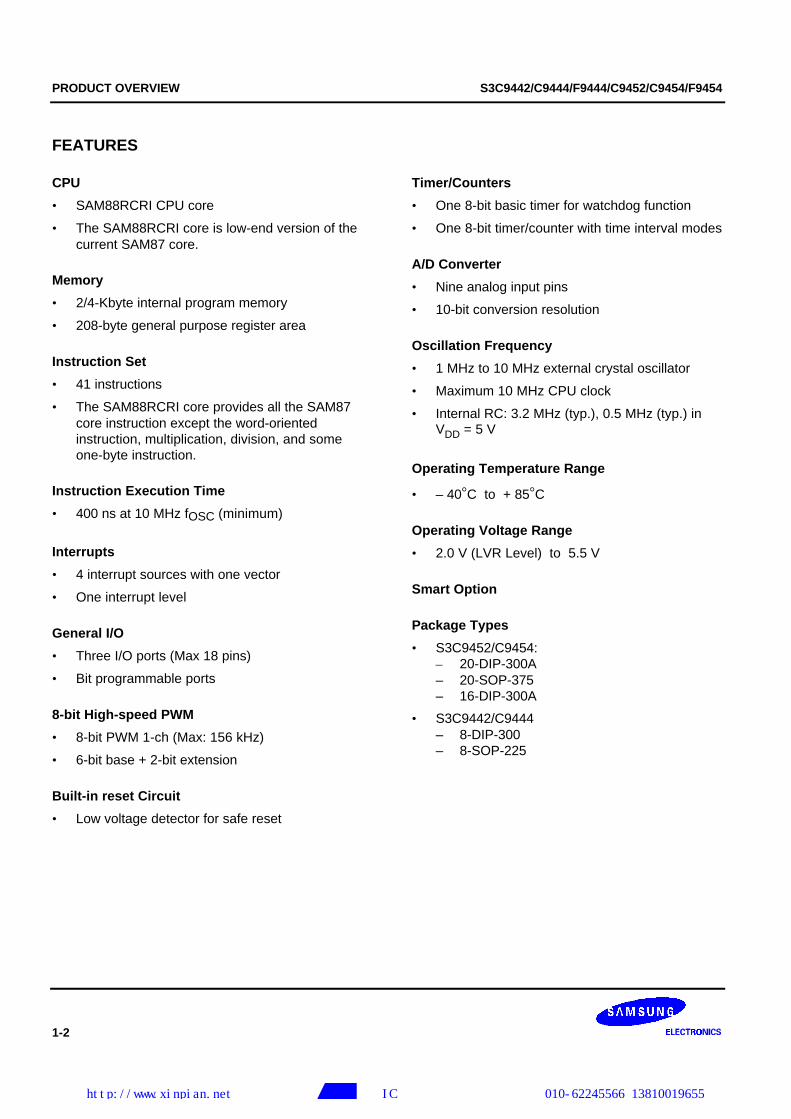
BLOCK DIAGRAM
88RCRISAMRI CPU
Port I/O andInterrupt Control
2 KB ROM4 KB ROM
208 ByteRegister file
Timer 0
ADC
PWM
XIN
XOUTOSC
BasicTimer
ADC0-ADC8
P0.6/PWM
Port 0
Port 2
Port 1
P0.0/ADC0/INT0
P0.1/ADC1/INT1
P0.2/ADC2
P0.7/ADC7
...
P1.0
P1.1
P1.2
P2.0/T0
P2.1
P2.6
...
NOTE: P1.2 is used as input only
Figure 1-1. Block Diagram
http://www.xinpian.net 提供单片机解密、IC解密、芯片解密业务 010-62245566 13810019655
PRODUCT OVERVIEW S3C9442/C9444/F9444/C9452/C9454/F9454
1-4
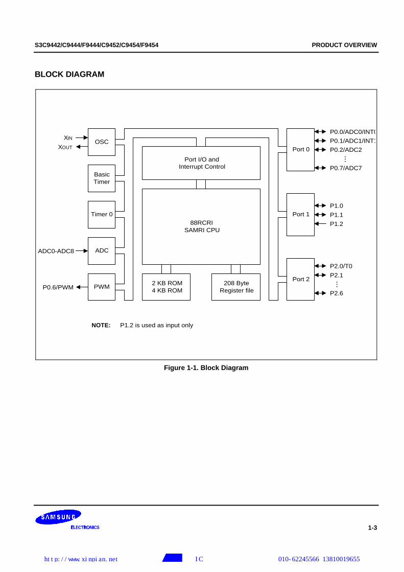
PIN ASSIGNMENTS
S3C9452/C9454
(20-DIP-300A/20-SOP-375)
20
19
18
17
16
15
14
13
12
11
1
2
3
4
5
6
7
8
9
10
VSS
XIN/P1.0
XOUT/P1.1
RESET/P1.2
P2.0/T0
P2.1
P2.2
P2.3
P2.4
P2.5
VDD
P0.0/ADC0/INT0
P0.1/ADC1/INT1
P0.2/ADC2
P0.3/ADC3
P0.4/ADC4
P0.5/ADC5
P0.6/ADC6/PWM
P0.7/ADC7
P2.6/ADC8/CLO
Figure 1-2. Pin Assignment Diagram (20-Pin DIP/SOP Package)
http://www.xinpian.net 提供单片机解密、IC解密、芯片解密业务 010-62245566 13810019655
S3C9442/C9444/F9444/C9452/C9454/F9454 PRODUCT OVERVIEW
1-5
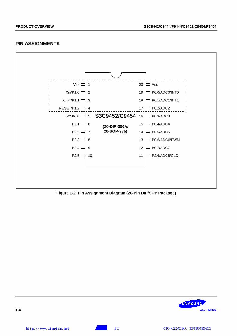
S3C9452/C9454
(16-DIP-300A)
VDD
P0.0/ADC0/INT0
P0.1/ADC1/INT1
P0.2/ADC2
P0.3/ADC3
P0.4/ADC4
P0.5/ADC5
P0.6/ADC6/PWM
16
15
14
13
12
11
10
9
VSS
XIN/P1.0
XOUT/P1.1
RESET/P1.2
P2.0/T0
P2.1
P2.2
P2.3
1
2
3
4
5
6
7
8
Figure 1-3. Pin Assignment Diagram (16-Pin DIP Package)
S3C9442/C9444
(8-DIP-3008-SOP-225)
VDD
P0.0/ADC0/INT0
P0.1/ADC1/INT1
P0.2/ADC2
8
7
6
5
VSS
XIN/P1.0
XOUT/P1.1
RESET/P1.2
1
2
3
4
Figure 1-4. Pin Assignment Diagram (8-Pin DIP/SOP Package)
http://www.xinpian.net 提供单片机解密、IC解密、芯片解密业务 010-62245566 13810019655
PRODUCT OVERVIEW S3C9442/C9444/F9444/C9452/C9454/F9454
1-6
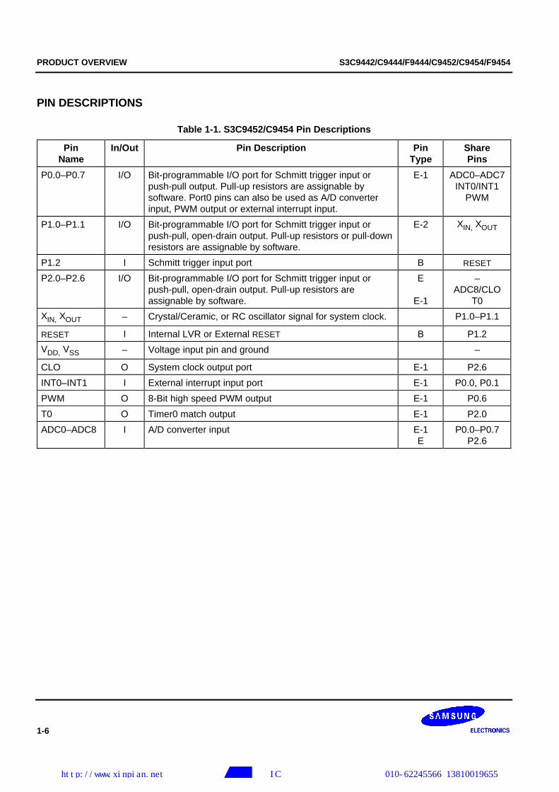
PIN DESCRIPTIONS
Table 1-1. S3C9452/C9454 Pin Descriptions
PinName
In/Out Pin Description PinType
SharePins
P0.0–P0.7 I/O Bit-programmable I/O port for Schmitt trigger input orpush-pull output. Pull-up resistors are assignable bysoftware. Port0 pins can also be used as A/D converterinput, PWM output or external interrupt input.
E-1 ADC0–ADC7INT0/INT1
PWM
P1.0–P1.1 I/O Bit-programmable I/O port for Schmitt trigger input orpush-pull, open-drain output. Pull-up resistors or pull-downresistors are assignable by software.
E-2 XIN, XOUT
P1.2 I Schmitt trigger input port B RESET
P2.0–P2.6 I/O Bit-programmable I/O port for Schmitt trigger input orpush-pull, open-drain output. Pull-up resistors areassignable by software.
E
E-1
–ADC8/CLO
T0
XIN, XOUT – Crystal/Ceramic, or RC oscillator signal for system clock. P1.0–P1.1
RESET I Internal LVR or External RESET B P1.2
VDD, VSS – Voltage input pin and ground –
CLO O System clock output port E-1 P2.6
INT0–INT1 I External interrupt input port E-1 P0.0, P0.1
PWM O 8-Bit high speed PWM output E-1 P0.6
T0 O Timer0 match output E-1 P2.0
ADC0–ADC8 I A/D converter input E-1E
P0.0–P0.7P2.6
http://www.xinpian.net 提供单片机解密、IC解密、芯片解密业务 010-62245566 13810019655
S3C9442/C9444/F9444/C9452/C9454/F9454 PRODUCT OVERVIEW
1-7
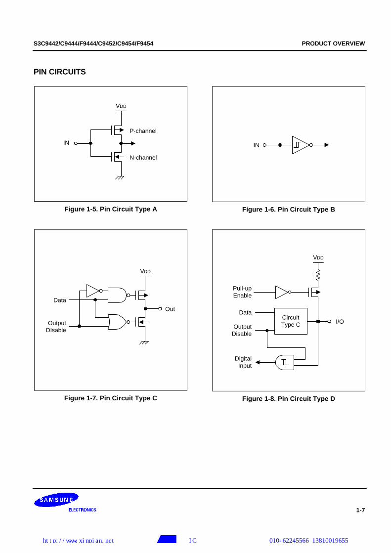
PIN CIRCUITS
VDD
IN
N-channel
P-channel
Figure 1-5. Pin Circuit Type A
IN
Figure 1-6. Pin Circuit Type B
VDD
Out
OutputDIsable
Data
Figure 1-7. Pin Circuit Type C
I/OOutput
Disable
DataCircuitType C
Pull-upEnable
VDD
DigitalInput
Figure 1-8. Pin Circuit Type D
http://www.xinpian.net 提供单片机解密、IC解密、芯片解密业务 010-62245566 13810019655
PRODUCT OVERVIEW S3C9442/C9444/F9444/C9452/C9454/F9454
1-8
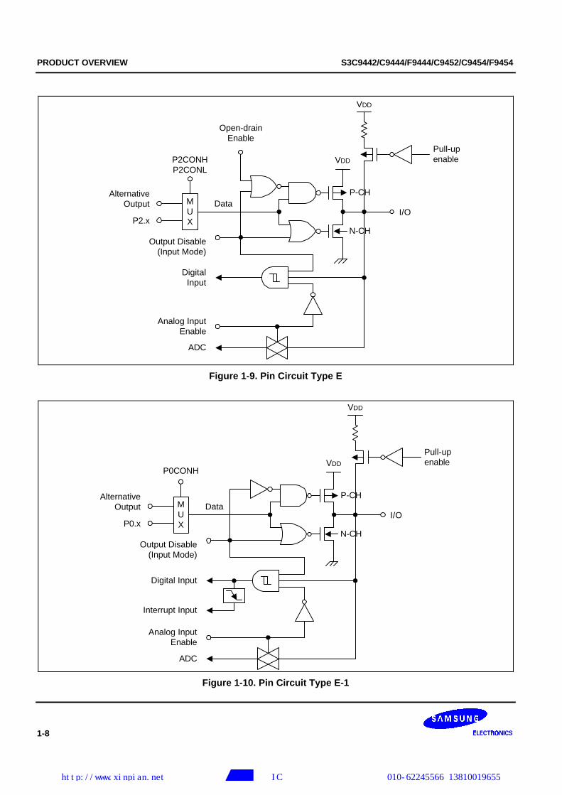
VDD
I/O
DigitalInput
P-CH
VDD
Open-drainEnable
Pull-upenable
Analog InputEnable
ADC
Output Disable(Input Mode)
DataMUX
AlternativeOutput
P2.x
P2CONHP2CONL
N-CH
Figure 1-9. Pin Circuit Type E
VDD
I/O
Digital Input
P-CH
VDD
Pull-upenable
Output Disable(Input Mode)
DataMUX
AlternativeOutput
P0.x
P0CONH
N-CH
Analog InputEnable
ADC
Interrupt Input
Figure 1-10. Pin Circuit Type E-1
http://www.xinpian.net 提供单片机解密、IC解密、芯片解密业务 010-62245566 13810019655
S3C9442/C9444/F9444/C9452/C9454/F9454 PRODUCT OVERVIEW
1-9
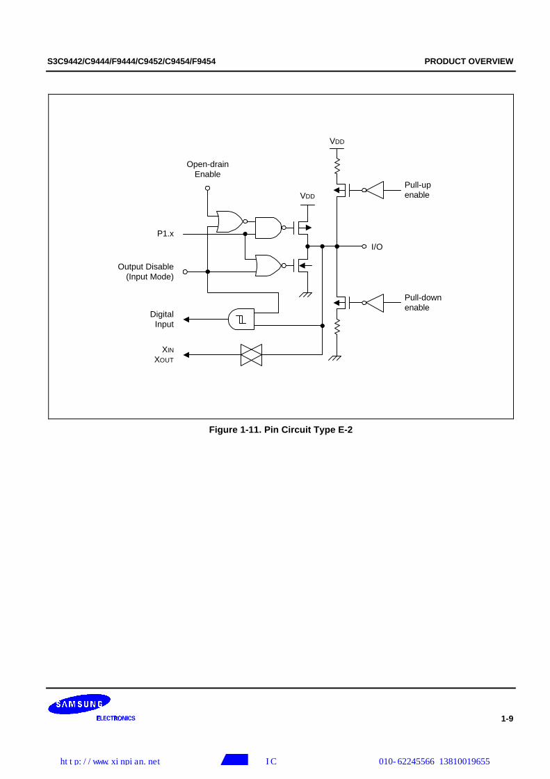
VDD
I/O
XIN
XOUT
VDD
Open-drainEnable
Output Disable(Input Mode)
P1.x
DigitalInput
Pull-upenable
Pull-downenable
Figure 1-11. Pin Circuit Type E-2
http://www.xinpian.net 提供单片机解密、IC解密、芯片解密业务 010-62245566 13810019655
S3C9442/C9444/F9444/C9452/C9454/F9454 ELECTRICAL DATA
13-1
13 ELECTRICAL DATA
OVERVIEW
In this section, the following S3C9442/C9444/C9452/C9454 electrical characteristics are presented in tables andgraphs:
— Absolute maximum ratings
— D.C. electrical characteristics
— A.C. electrical characteristics
— Input Timing Measurement Points
— Oscillator characteristics
— Oscillation stabilization time
— Operating Voltage Range
— Schmitt trigger input characteristics
— Data retention supply voltage in Stop mode
— Stop mode release timing when initiated by a RESET
— A/D converter electrical characteristics
— LVR circuit characteristics
— LVR reset Timing
http://www.xinpian.net 提供单片机解密、IC解密、芯片解密业务 010-62245566 13810019655
ELECTRICAL DATA S3C9442/C9444/F9444/C9452/C9454/F9454
13-2
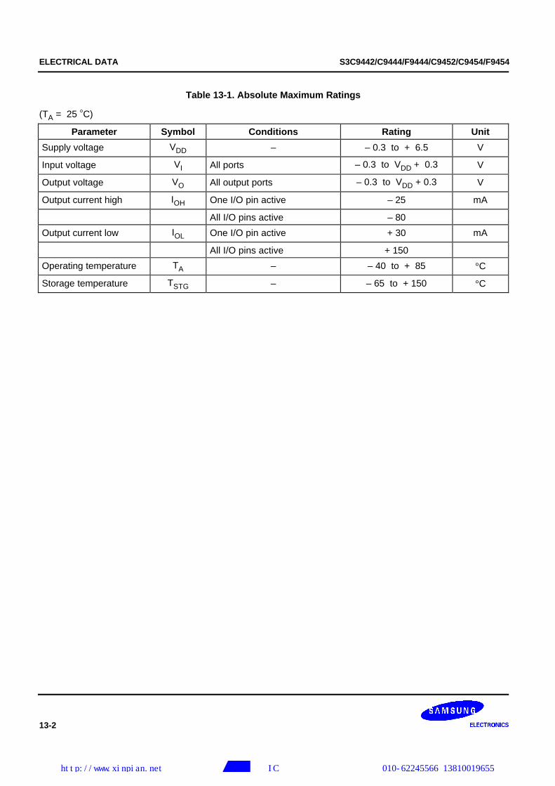
Table 13-1. Absolute Maximum Ratings
(TA = 25 °C)
Parameter Symbol Conditions Rating Unit
Supply voltage VDD – – 0.3 to + 6.5 V
Input voltage VI All ports – 0.3 to VDD + 0.3 V
Output voltage VO All output ports – 0.3 to VDD + 0.3 V
Output current high IOH One I/O pin active – 25 mA
All I/O pins active – 80
Output current low IOL One I/O pin active + 30 mA
All I/O pins active + 150
Operating temperature TA – – 40 to + 85 °C
Storage temperature TSTG – – 65 to + 150 °C
http://www.xinpian.net 提供单片机解密、IC解密、芯片解密业务 010-62245566 13810019655
S3C9442/C9444/F9444/C9452/C9454/F9454 ELECTRICAL DATA
13-3
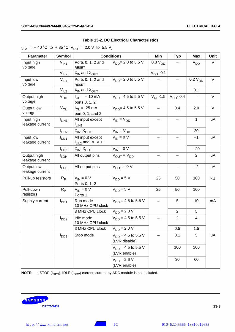
Table 13-2. DC Electrical Characteristics
(TA = – 40 °C to + 85 °C, VDD = 2.0 V to 5.5 V)
Parameter Symbol Conditions Min Typ Max Unit
Input highvoltage
VIH1 Ports 0, 1, 2 andRESET
VDD= 2.0 to 5.5 V 0.8 VDD – VDD V
VIH2 XIN and XOUT VDD- 0.1
Input lowvoltage
VIL1 Ports 0, 1, 2 andRESET
VDD= 2.0 to 5.5 V – – 0.2 VDD V
VIL2 XIN and XOUT 0.1
Output highvoltage
VOH IOH = – 10 mA
ports 0, 1, 2
VDD= 4.5 to 5.5 V VDD-1.5 VDD- 0.4 – V
Output lowvoltage
VOL IOL = 25 mA
port 0, 1, and 2
VDD= 4.5 to 5.5 V – 0.4 2.0 V
Input highleakage current
ILIH1 All input exceptILIH2
VIN = VDD – – 1 uA
ILIH2 XIN, XOUT VIN = VDD 20
Input lowleakage current
ILIL1 All input exceptILIL2 and RESET
VIN = 0 V – – –1 uA
ILIL2 XIN, XOUT VIN = 0 V –20
Output highleakage current
ILOH All output pins VOUT = VDD – – 2 uA
Output lowleakage current
ILOL All output pins VOUT = 0 V – – –2 uA
Pull-up resistors RP VIN = 0 V
Ports 0, 1, 2
VDD = 5 V 25 50 100 kΩ
Pull-downresistors
RP VIN = 0 V
Ports 1
VDD = 5 V 25 50 100
Supply current IDD1 Run mode10 MHz CPU clock
VDD = 4.5 to 5.5 V – 5 10 mA
3 MHz CPU clock VDD = 2.0 V 2 5
IDD2 Idle mode10 MHz CPU clock
VDD = 4.5 to 5.5 V – 2 4
3 MHz CPU clock VDD = 2.0 V 0.5 1.5
IDD3 Stop mode VDD = 4.5 to 5.5 V
(LVR disable)
– 0.1 5 uA
VDD = 4.5 to 5.5 V
(LVR enable)
100 200
VDD = 2.6 V
(LVR enable)
30 60
NOTE: In STOP (IDD3), IDLE (IDD2) current, current by ADC module is not included.
http://www.xinpian.net 提供单片机解密、IC解密、芯片解密业务 010-62245566 13810019655
ELECTRICAL DATA S3C9442/C9444/F9444/C9452/C9454/F9454
13-4
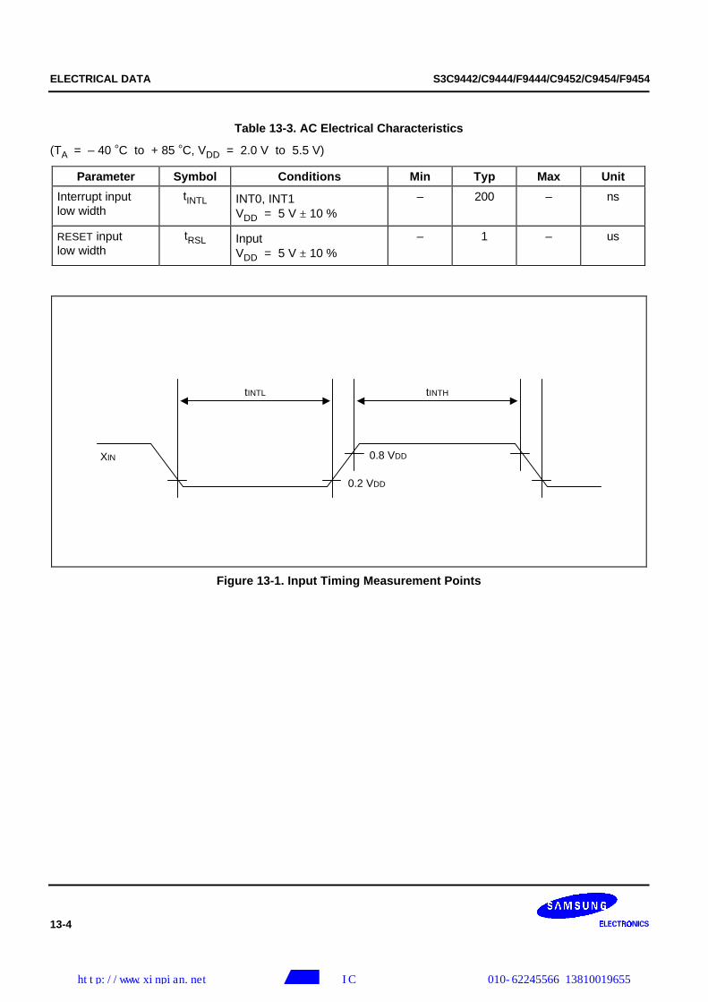
Table 13-3. AC Electrical Characteristics
(TA = – 40 °C to + 85 °C, VDD = 2.0 V to 5.5 V)
Parameter Symbol Conditions Min Typ Max Unit
Interrupt inputlow width
tINTL INT0, INT1VDD = 5 V ± 10 %
– 200 – ns
RESET inputlow width
tRSL InputVDD = 5 V ± 10 %
– 1 – us
tINTL tINTH
XIN 0.8 VDD
0.2 VDD
Figure 13-1. Input Timing Measurement Points
http://www.xinpian.net 提供单片机解密、IC解密、芯片解密业务 010-62245566 13810019655
S3C9442/C9444/F9444/C9452/C9454/F9454 ELECTRICAL DATA
13-5
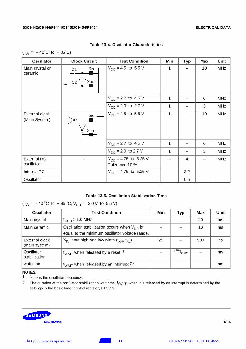
Table 13-4. Oscillator Characteristics
(TA = – 40°C to + 85°C)
Oscillator Clock Circuit Test Condition Min Typ Max Unit
Main crystal orceramic
XIN
XOUT
C1
C2
VDD = 4.5 to 5.5 V 1 – 10 MHz
VDD = 2.7 to 4.5 V 1 – 6 MHz
VDD = 2.0 to 2.7 V 1 – 3 MHz
External clock(Main System)
XIN
XOUT
VDD = 4.5 to 5.5 V 1 – 10 MHz
VDD = 2.7 to 4.5 V 1 – 6 MHz
VDD = 2.0 to 2.7 V 1 – 3 MHz
External RCoscillator
– VDD = 4.75 to 5.25 V
Tolerance:10 %– 4 – MHz
Internal RC VDD = 4.75 to 5.25 V 3.2
Oscillator 0.5
Table 13-5. Oscillation Stabilization Time
(TA = - 40 °C to + 85 °C, VDD = 3.0 V to 5.5 V)
Oscillator Test Condition Min Typ Max Unit
Main crystal fOSC > 1.0 MHz – – 20 ms
Main ceramic Oscillation stabilization occurs when VDD is
equal to the minimum oscillator voltage range.– – 10 ms
External clock(main system)
XIN input high and low width (tXH, tXL) 25 – 500 ns
Oscillatorstabilization
tWAIT when released by a reset (1) – 216/fOSC – ms
wait time tWAIT when released by an interrupt (2) – – – ms
NOTES:1. fOSC is the oscillator frequency.
2. The duration of the oscillator stabilization wait time, tWAIT, when it is released by an interrupt is determined by the settings in the basic timer control register, BTCON.
http://www.xinpian.net 提供单片机解密、IC解密、芯片解密业务 010-62245566 13810019655
ELECTRICAL DATA S3C9442/C9444/F9444/C9452/C9454/F9454
13-6
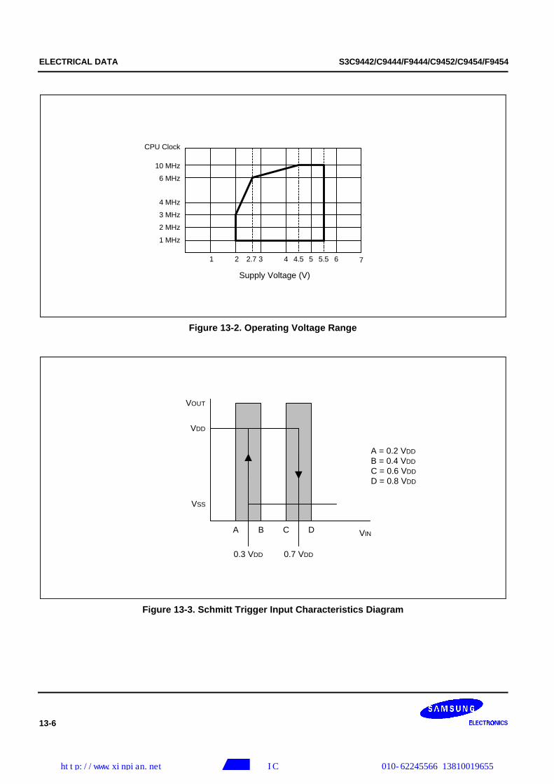
10 MHz
CPU Clock
6 MHz
1 MHz
1 2 3 4 5 6 7
Supply Voltage (V)
2 MHz
3 MHz
4 MHz
2.7 5.54.5
Figure 13-2. Operating Voltage Range
VSS
A
A = 0.2 VDD
B = 0.4 VDD
C = 0.6 VDD
D = 0.8 VDD
VDD
VOUT
VINB C D
0.3 VDD 0.7 VDD
Figure 13-3. Schmitt Trigger Input Characteristics Diagram
http://www.xinpian.net 提供单片机解密、IC解密、芯片解密业务 010-62245566 13810019655
S3C9442/C9444/F9444/C9452/C9454/F9454 ELECTRICAL DATA
13-7
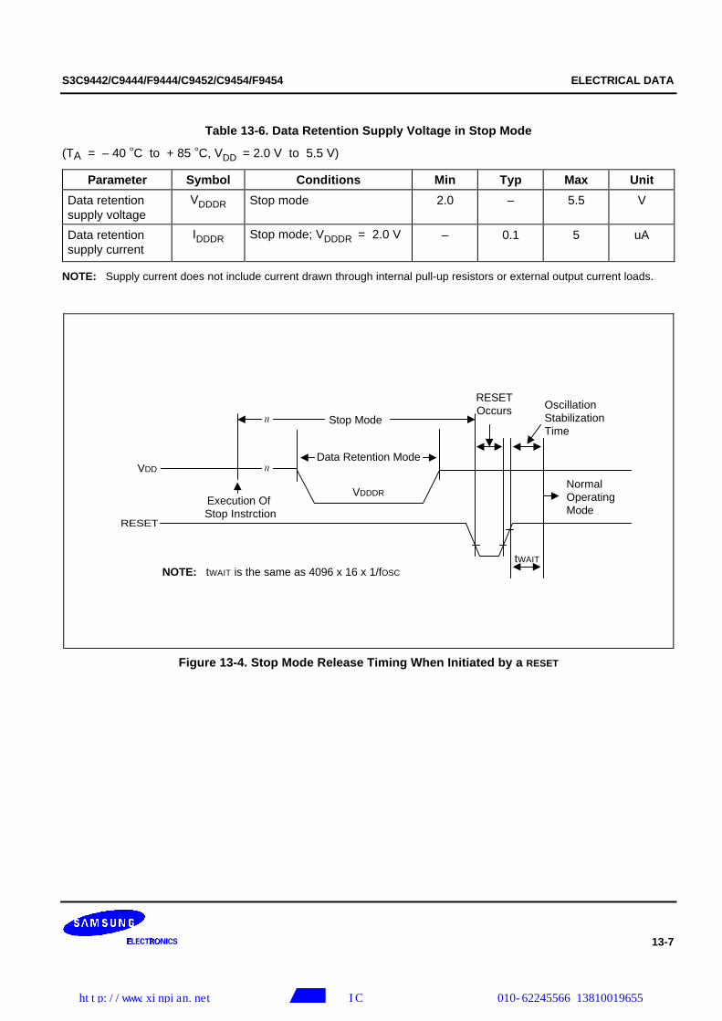
Table 13-6. Data Retention Supply Voltage in Stop Mode
(TA = – 40 °C to + 85 °C, VDD = 2.0 V to 5.5 V)
Parameter Symbol Conditions Min Typ Max Unit
Data retentionsupply voltage
VDDDR Stop mode 2.0 – 5.5 V
Data retentionsupply current
IDDDR Stop mode; VDDDR = 2.0 V – 0.1 5 uA
NOTE: Supply current does not include current drawn through internal pull-up resistors or external output current loads.
Data Retention Mode
VDDDRExecution Of
Stop Instrction
VDD
NormalOperatingMode
OscillationStabilizationTime
Stop Mode
tWAIT
RESET
RESETOccurs
NOTE: tWAIT is the same as 4096 x 16 x 1/fOSC
~ ~~ ~
Figure 13-4. Stop Mode Release Timing When Initiated by a RESET
http://www.xinpian.net 提供单片机解密、IC解密、芯片解密业务 010-62245566 13810019655
ELECTRICAL DATA S3C9442/C9444/F9444/C9452/C9454/F9454
13-8
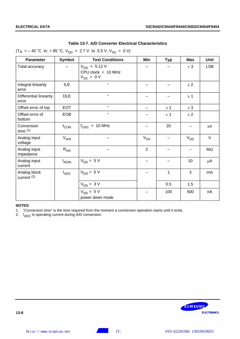
Table 13-7. A/D Converter Electrical Characteristics
(TA = – 40 °C to + 85 °C, VDD = 2.7 V to 5.5 V, VSS = 0 V)
Parameter Symbol Test Conditions Min Typ Max Unit
Total accuracy – VDD = 5.12 V
CPU clock = 10 MHzVSS = 0 V
– – ± 3 LSB
Integral linearityerror
ILE ″ – – ± 2
Differential linearityerror
DLE ″ – – ± 1
Offset error of top EOT ″ – ± 1 ± 3
Offset error ofbottom
EOB ″ – ± 1 ± 2
Conversiontime (1)
tCON fOSC = 10 MHz – 20 – µs
Analog inputvoltage
VIAN – VSS – VDD V
Analog inputimpedance
RAN – 2 – – MΩ
Analog inputcurrent
IADIN VDD = 5 V – – 10 µA
Analog blockcurrent (2)
IADC VDD = 5 V – 1 3 mA
VDD = 3 V 0.5 1.5
VDD = 5 V
power down mode– 100 500 nA
NOTES:1. “Conversion time” is the time required from the moment a conversion operation starts until it ends.2. IADC is operating current during A/D conversion.
http://www.xinpian.net 提供单片机解密、IC解密、芯片解密业务 010-62245566 13810019655
S3C9442/C9444/F9444/C9452/C9454/F9454 ELECTRICAL DATA
13-9
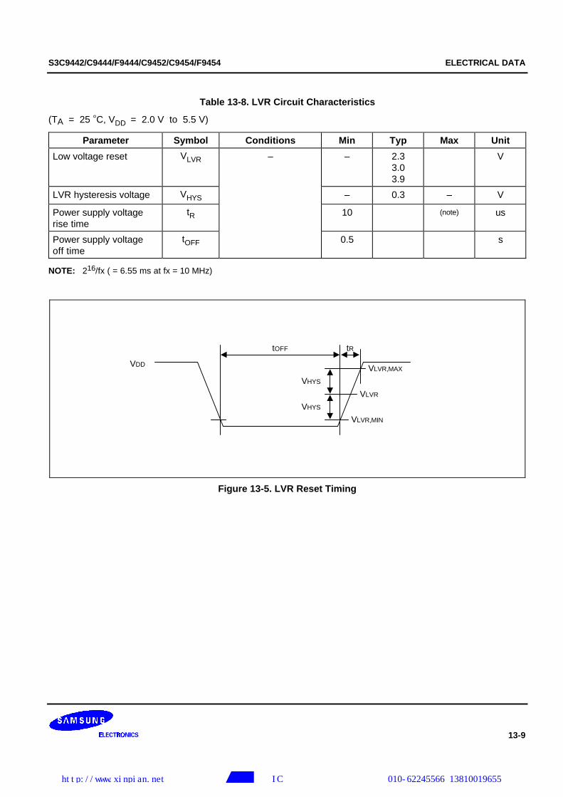
Table 13-8. LVR Circuit Characteristics
(TA = 25 °C, VDD = 2.0 V to 5.5 V)
Parameter Symbol Conditions Min Typ Max Unit
Low voltage reset VLVR – – 2.33.03.9
V
LVR hysteresis voltage VHYS – 0.3 – V
Power supply voltagerise time
tR 10 (note) us
Power supply voltageoff time
tOFF 0.5 s
NOTE: 216/fx ( = 6.55 ms at fx = 10 MHz)
VDD VLVR,MAX
VHYS
VHYS
VLVR
VLVR,MIN
tOFF tR
Figure 13-5. LVR Reset Timing
http://www.xinpian.net 提供单片机解密、IC解密、芯片解密业务 010-62245566 13810019655
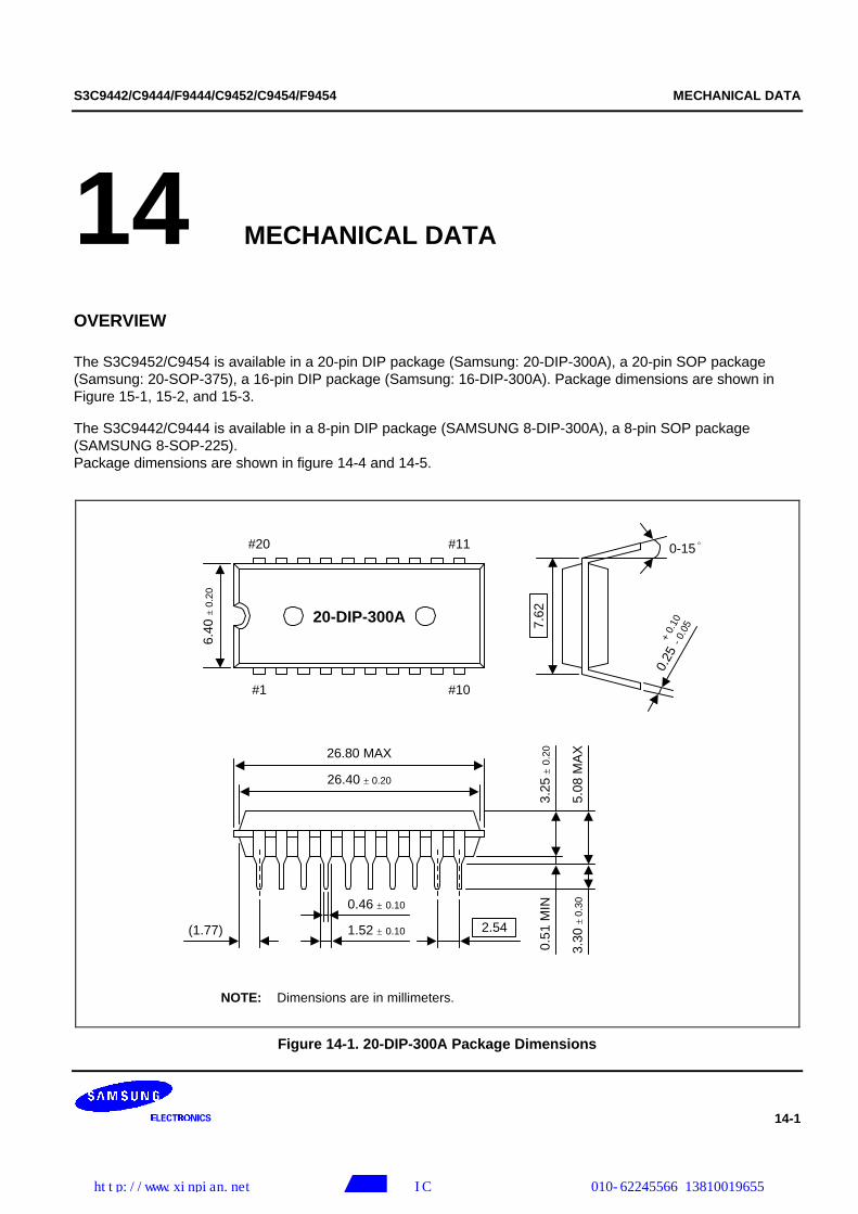
S3C9442/C9444/F9444/C9452/C9454/F9454 MECHANICAL DATA
14-1
14 MECHANICAL DATA
OVERVIEW
The S3C9452/C9454 is available in a 20-pin DIP package (Samsung: 20-DIP-300A), a 20-pin SOP package(Samsung: 20-SOP-375), a 16-pin DIP package (Samsung: 16-DIP-300A). Package dimensions are shown inFigure 15-1, 15-2, and 15-3.
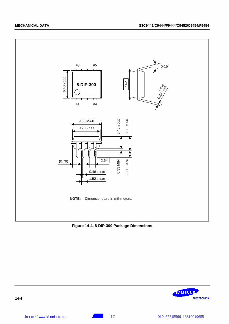
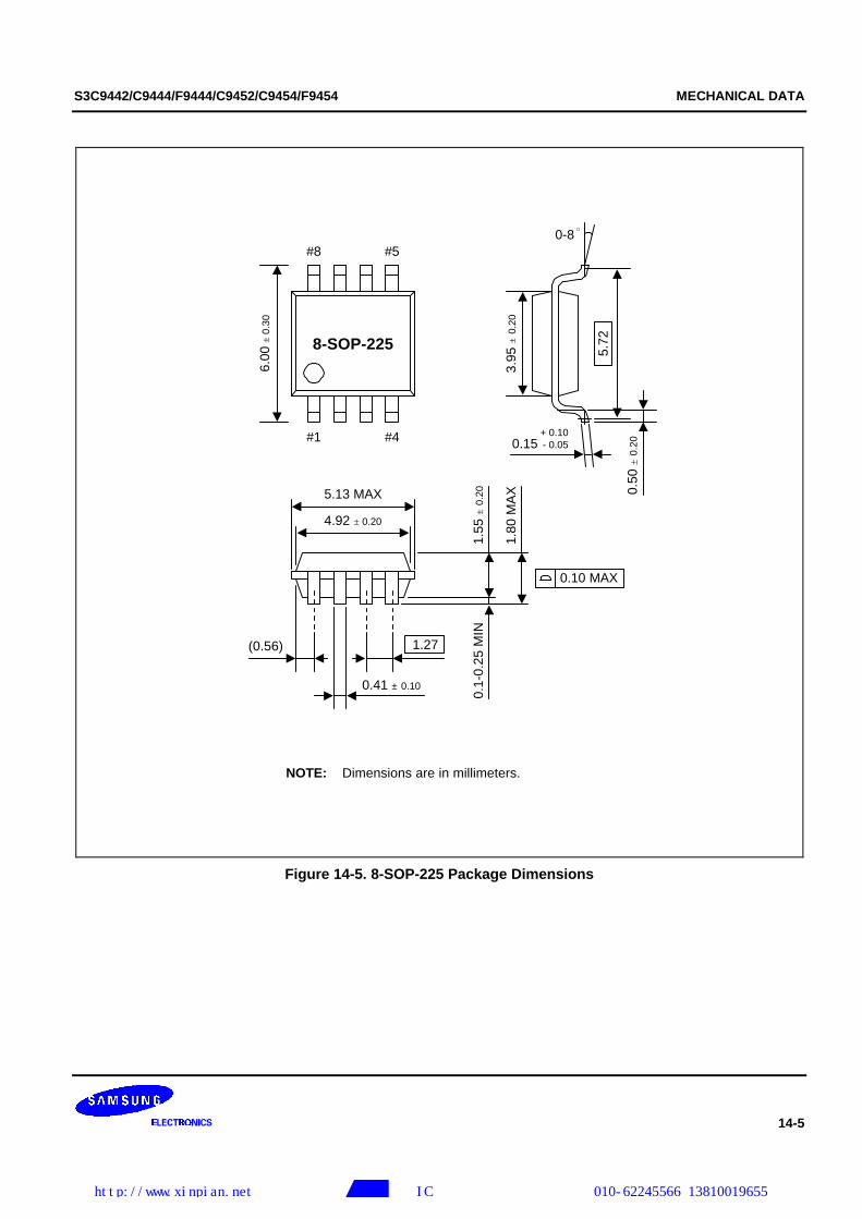
The S3C9442/C9444 is available in a 8-pin DIP package (SAMSUNG 8-DIP-300A), a 8-pin SOP package(SAMSUNG 8-SOP-225).Package dimensions are shown in figure 14-4 and 14-5.
NOTE: Dimensions are in millimeters.
26.80 MAX
26.40 ± 0.20
(1.77)
20-DIP-300A
6.40
± 0
.20
#20
#1
0.46 ± 0.10
1.52 ± 0.10
#11
#10
0-15
0.25
+ 0.
10- 0
.057.
62
2.54
0.51
MIN
3.30
± 0
.30
3.25
± 0
.20
5.08
MA
X
Figure 14-1. 20-DIP-300A Package Dimensions
http://www.xinpian.net 提供单片机解密、IC解密、芯片解密业务 010-62245566 13810019655
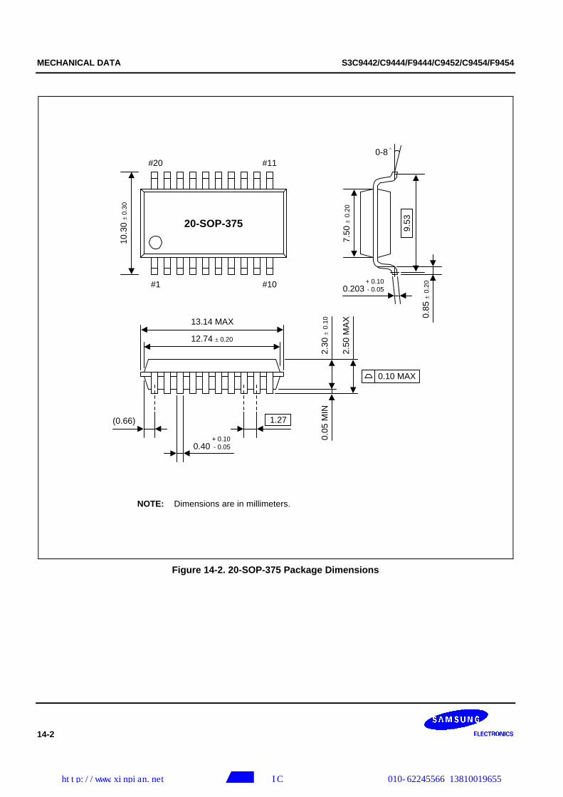
MECHANICAL DATA S3C9442/C9444/F9444/C9452/C9454/F9454
14-2
NOTE: Dimensions are in millimeters.
20-SOP-375
10.3
0 ±
0.30
#11#20
#1 #10
13.14 MAX
12.74 ± 0.20
(0.66)
0-8
0.203+ 0.10- 0.05
9.53
7.50
± 0
.20
0.85
± 0
.20
0.05
MIN
2.30
± 0
.10
2.50
MA
X
0.40
0.10 MAX
+ 0.10- 0.05
1.27
Figure 14-2. 20-SOP-375 Package Dimensions
http://www.xinpian.net 提供单片机解密、IC解密、芯片解密业务 010-62245566 13810019655
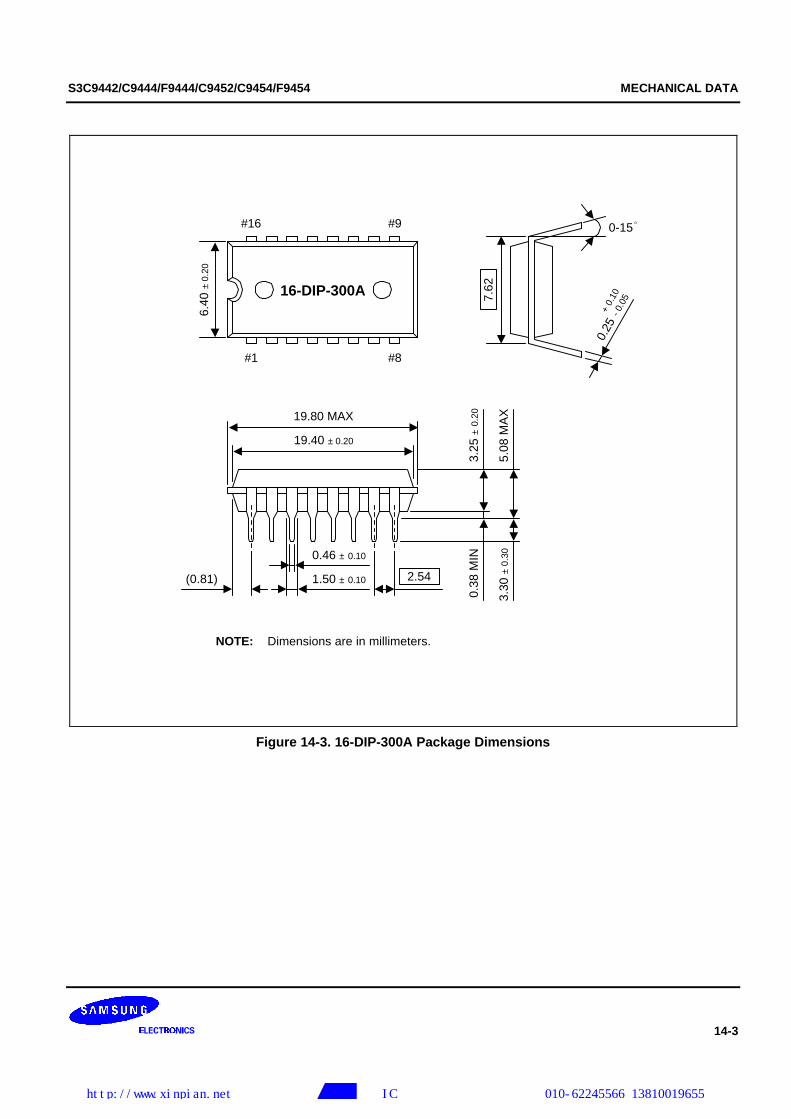
S3C9442/C9444/F9444/C9452/C9454/F9454 MECHANICAL DATA
14-3
NOTE: Dimensions are in millimeters.
19.80 MAX
19.40 ± 0.20
(0.81)
6.40
± 0
.20
#16
#1
16-DIP-300A
0.46 ± 0.10
1.50 ± 0.10
#9
#8
0-15
0.25
+ 0.
10- 0
.057.
62
2.54
0.38
MIN
3.30
± 0
.30
3.25
± 0
.20
5.08
MA
X
Figure 14-3. 16-DIP-300A Package Dimensions
http://www.xinpian.net 提供单片机解密、IC解密、芯片解密业务 010-62245566 13810019655
MECHANICAL DATA S3C9442/C9444/F9444/C9452/C9454/F9454
14-4
NOTE: Dimensions are in millimeters.
9.60 MAX
9.20 ± 0.20
2.54
0.46 ± 0.10
1.52 ± 0.10
(0.79)
0.33
MIN
3.30
± 0
.30
3.40
± 0
.20
5.08
MA
X
0-15
0.25
+ 0.
10- 0
.057.
628-DIP-300
6.40
± 0
.20
#8
#1
#5
#4
Figure 14-4. 8-DIP-300 Package Dimensions
http://www.xinpian.net 提供单片机解密、IC解密、芯片解密业务 010-62245566 13810019655
S3C9442/C9444/F9444/C9452/C9454/F9454 MECHANICAL DATA
14-5
NOTE: Dimensions are in millimeters.
8-SOP-225
6.00
± 0
.30
#5#8
#1 #4
5.13 MAX
4.92 ± 0.20
(0.56) 1.27
0.1-
0.25
MIN
1.55
± 0
.20
1.80
MA
X
0.41 ± 0.10
0-8
0.15+ 0.10- 0.05
5.72
3.95
± 0
.20
0.50
± 0
.20
0.10 MAX
Figure 14-5. 8-SOP-225 Package Dimensions
http://www.xinpian.net 提供单片机解密、IC解密、芯片解密业务 010-62245566 13810019655
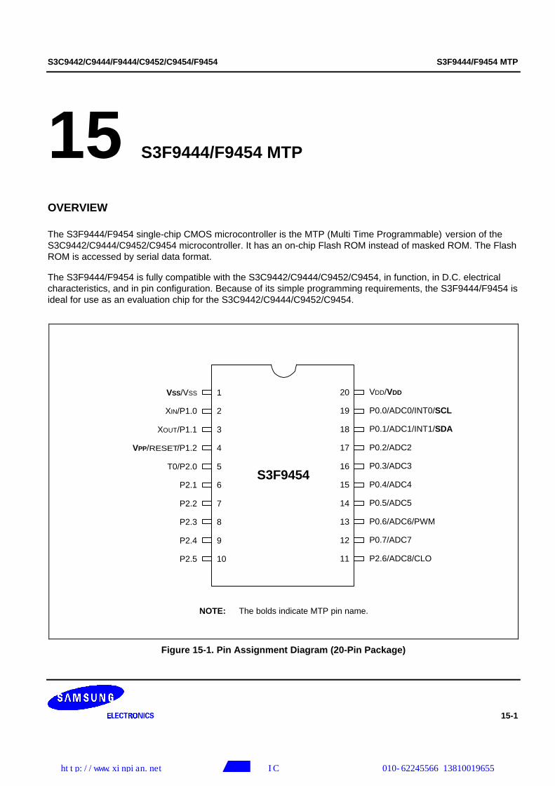
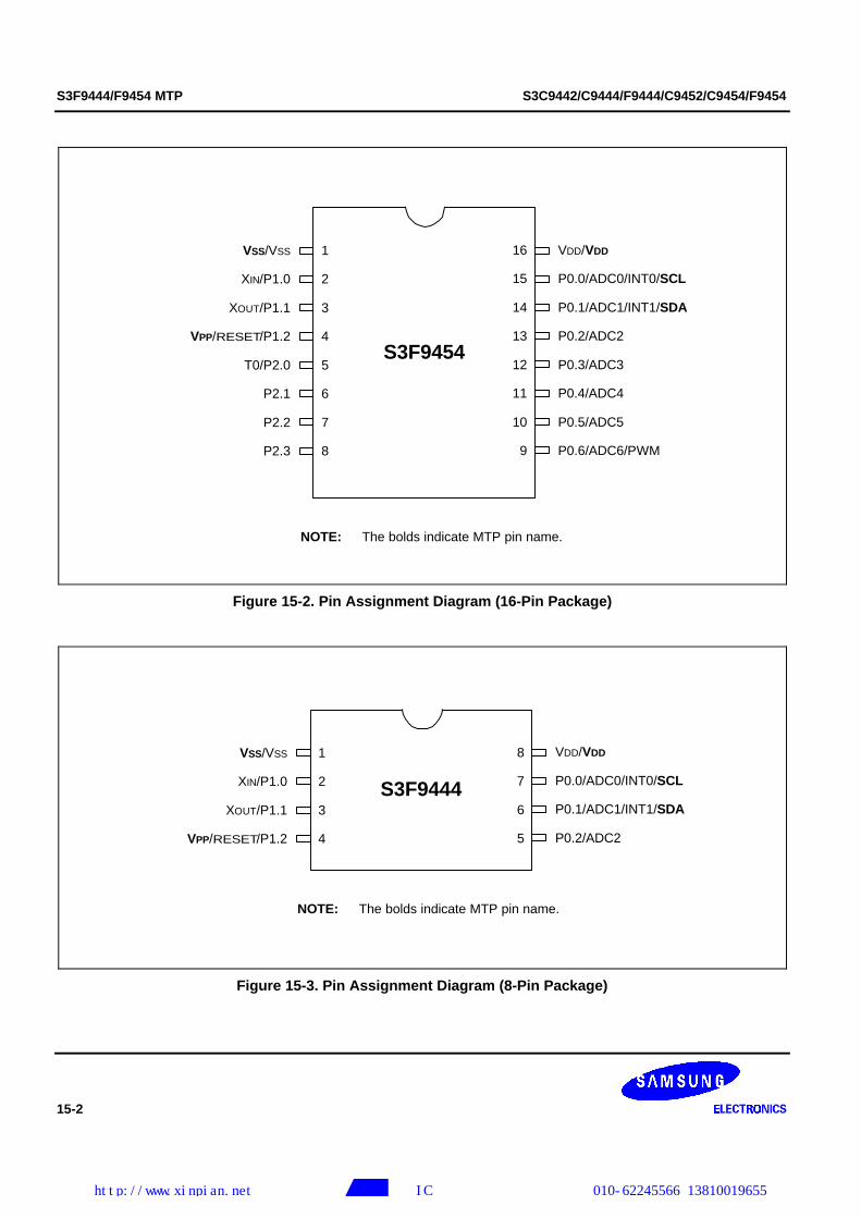
S3C9442/C9444/F9444/C9452/C9454/F9454 S3F9444/F9454 MTP
15-1
15 S3F9444/F9454 MTP
OVERVIEW
The S3F9444/F9454 single-chip CMOS microcontroller is the MTP (Multi Time Programmable) version of theS3C9442/C9444/C9452/C9454 microcontroller. It has an on-chip Flash ROM instead of masked ROM. The FlashROM is accessed by serial data format.
The S3F9444/F9454 is fully compatible with the S3C9442/C9444/C9452/C9454, in function, in D.C. electricalcharacteristics, and in pin configuration. Because of its simple programming requirements, the S3F9444/F9454 isideal for use as an evaluation chip for the S3C9442/C9444/C9452/C9454.
VDD/VDD
P0.0/ADC0/INT0/SCL
P0.1/ADC1/INT1/SDA
P0.2/ADC2
P0.3/ADC3
P0.4/ADC4
P0.5/ADC5
P0.6/ADC6/PWM
P0.7/ADC7
P2.6/ADC8/CLO
S3F9454
20
19
18
17
16
15
14
13
12
11
VSS/VSS
XIN/P1.0
XOUT/P1.1
VPP/RESET/P1.2
T0/P2.0
P2.1
P2.2
P2.3
P2.4
P2.5
1
2
3
4
5
6
7
8
9
10
NOTE: The bolds indicate MTP pin name.
Figure 15-1. Pin Assignment Diagram (20-Pin Package)
http://www.xinpian.net 提供单片机解密、IC解密、芯片解密业务 010-62245566 13810019655
S3F9444/F9454 MTP S3C9442/C9444/F9444/C9452/C9454/F9454
15-2
S3F9454
VDD/VDD
P0.0/ADC0/INT0/SCL
P0.1/ADC1/INT1/SDA
P0.2/ADC2
P0.3/ADC3
P0.4/ADC4
P0.5/ADC5
P0.6/ADC6/PWM
16
15
14
13
12
11
10
9
VSS/VSS
XIN/P1.0
XOUT/P1.1
VPP/RESET/P1.2
T0/P2.0
P2.1
P2.2
P2.3
1
2
3
4
5
6
7
8
NOTE: The bolds indicate MTP pin name.
Figure 15-2. Pin Assignment Diagram (16-Pin Package)
S3F9444
VDD/VDD
P0.0/ADC0/INT0/SCL
P0.1/ADC1/INT1/SDA
P0.2/ADC2
8
7
6
5
VSS/VSS
XIN/P1.0
XOUT/P1.1
VPP/RESET/P1.2
1
2
3
4
NOTE: The bolds indicate MTP pin name.
Figure 15-3. Pin Assignment Diagram (8-Pin Package)
http://www.xinpian.net 提供单片机解密、IC解密、芯片解密业务 010-62245566 13810019655
S3C9442/C9444/F9444/C9452/C9454/F9454 S3F9444/F9454 MTP
15-3
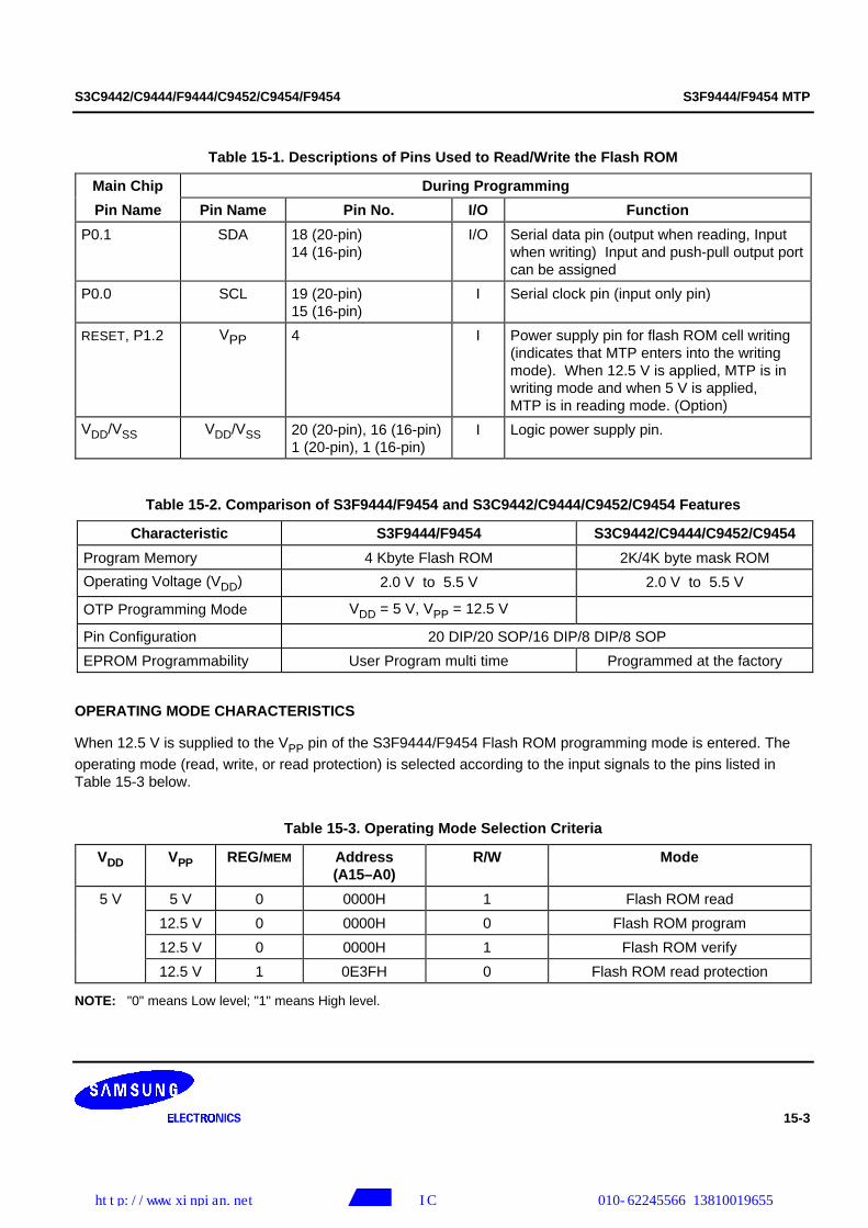
Table 15-1. Descriptions of Pins Used to Read/Write the Flash ROM
Main Chip During Programming
Pin Name Pin Name Pin No. I/O Function
P0.1 SDA 18 (20-pin)14 (16-pin)
I/O Serial data pin (output when reading, Inputwhen writing) Input and push-pull output portcan be assigned
P0.0 SCL 19 (20-pin)15 (16-pin)
I Serial clock pin (input only pin)
RESET, P1.2 VPP 4 I Power supply pin for flash ROM cell writing(indicates that MTP enters into the writingmode). When 12.5 V is applied, MTP is inwriting mode and when 5 V is applied,MTP is in reading mode. (Option)
VDD/VSS VDD/VSS 20 (20-pin), 16 (16-pin)1 (20-pin), 1 (16-pin)
I Logic power supply pin.
Table 15-2. Comparison of S3F9444/F9454 and S3C9442/C9444/C9452/C9454 Features
Characteristic S3F9444/F9454 S3C9442/C9444/C9452/C9454
Program Memory 4 Kbyte Flash ROM 2K/4K byte mask ROM
Operating Voltage (VDD) 2.0 V to 5.5 V 2.0 V to 5.5 V
OTP Programming Mode VDD = 5 V, VPP = 12.5 V
Pin Configuration 20 DIP/20 SOP/16 DIP/8 DIP/8 SOP
EPROM Programmability User Program multi time Programmed at the factory
OPERATING MODE CHARACTERISTICS
When 12.5 V is supplied to the VPP pin of the S3F9444/F9454 Flash ROM programming mode is entered. The
operating mode (read, write, or read protection) is selected according to the input signals to the pins listed inTable 15-3 below.
Table 15-3. Operating Mode Selection Criteria
VDD VPP REG/MEM Address(A15–A0)
R/W Mode
5 V 5 V 0 0000H 1 Flash ROM read
12.5 V 0 0000H 0 Flash ROM program
12.5 V 0 0000H 1 Flash ROM verify
12.5 V 1 0E3FH 0 Flash ROM read protection
NOTE: "0" means Low level; "1" means High level.
http://www.xinpian.net 提供单片机解密、IC解密、芯片解密业务 010-62245566 13810019655


![Qht QHv PDFu5[Pe hcb g/cÐO UFcdn02.foxitsoftware.com/pub/foxit/manual/chs/foxit profile-cn.pdf · 2001^t kc_ b zËy ]Þy f oNö_SÑg PQlSø W( VýR R)y \](https://img.pdfslide.us/doc/110x75/5b8a543c7f8b9ac1328bebc2/qht-qhv-pdfu5pe-hcb-gcdo-profile-cnpdf-2001t-kc-b-zey-by-f-onoesng.jpg)