Embed Size (px)
Citation preview

S1C31D50 (rev1.0)
32-bit Single Chip Microcontroller ARM® 32-bit RISC CPUcore Cortex®-M0+ Embedded 192K bytes Flash memory(Program & Sound ROM), 8K bytes RAM “Voice/Audio Play"(2ch mixing play, Voice Speed Conversion w/o CPU resource) “Self Memory Check” w/o CPU resource
■ DESCRIPTIONS
The S1C31D50 is a 32-bit ARM® Cortex®-M0+ MCU which integrates a specific hardware block called the HW Processor. The HW Processor can perform 2ch Voice/Audio Play, Voice Speed Conversion, and Self Memory Check without using any CPU resource. The S1C31D50 is suitable for home electronics, white goods, and battery-based products which require voice and audio playback.
With the HW Processor, low memory footprint and multi-language support are achievable because of its integrated high-compression algorithm for voice and audio.
Furthermore, the EPSON Voice Creation PC tool makes development without studio recording easy. (EPSON Voice Creation PC tool supports English, Chinese, Japanese, and Korean female voices.)
■ FEATURES Model S1C31D50 CPU CPU core ARM® 32-bit RISC CPU core Cortex®-M0+ Other Serial-wire debug ports (SW-DP) and a micro trace buffer (MTB) included Embedded Flash memory Capacity 192K bytes (for both instructions and data) Erase/program count 1,000 times (min.) * When being programmed by the dedicated flash loader Other On-board programming function
Flash programming voltage can be generated internally. Embedded RAMs General-purpose RAM 8K bytes + 14K bytes (when HW Processor is not active) Instruction cache 512 bytes HW Processor Voice Audio Play FUNCTION Voice/Audio Algorithm EPSON high quality & High compress algorithm Play channels 2ch mixing support(suitable for background music + Voice play Sampling Frequency 15.625kHz, (suitable for background music + Voice play) Bitrate 16/24/32/40 kbps Voice Speed Conversion 75% - 125% (5% step) Self Memory Check FUNCTION On Chip RAM Check W/R Check, MARCH-C On Chip Flash check Checksum, CRC External SPI-Flash Check Checksum, CRC Sound DAC Sampling Frequency 15.625kHz Serial interfaces UART (UART3) 3 channels
Baud-rate generator included, IrDA1.0 supported Open drain output, signal polarity, and baud rate division ratio are configurable. Infrared communication carrier modulation output function
Synchronous serial interface (SPIA) 3 channels 2 to 16-bit variable data length The 16-bit timer (T16) can be used for the baud-rate generator in master mode.
Quad synchronous serial interface (QSPI) 1 channel Supports single, dual, and quad transfer modes. Low CPU overhead memory mapped access mode that can directly read data from the external flash memory with XIP (eXecute-In-Place) mode.
I2C (I2C) 3 channels Baud-rate generator included
DMA Controller (DMAC) Number of channels 4 channels Data transfer path Memory to memory, memory to peripheral, and peripheral to memory Transfer mode Basic, ping-pong, scatter-gather DMA trigger source UART3, SPIA, QSPI, I2C, T16B, ADC12A, and software
®

S1C31D50
2
Clock generator (CLG) System clock source 4 sources (IOSC/OSC1/OSC3/EXOSC) System clock frequency (operating frequency) VD1 voltage mode = mode0: 16 MHz (max.)
VD1 voltage mode = mode1: 2 MHz (max.) IOSC oscillator circuit (boot clock source) VD1 voltage mode = mode0: 8/2/1 MHz (typ.) software selectable
VD1 voltage mode = mode1: 2/1 MHz (typ.) software selectable 10 µs (max.) starting time (time from cancelation of SLEEP state to vector table read by the CPU)
OSC1 oscillator circuit 32.768 kHz (typ.) crystal oscillator 32kHz (typ.) embedded oscillator Oscillation stop detection circuit included
OSC3 oscillator circuit 16 MHz (max.) crystal/ceramic oscillator 16/8/4MHz(typ) embedded oscillator
EXOSC clock input 16 MHz (max.) square or sine wave input Other Configurable system clock division ratio
Configurable system clock used at wake up from SLEEP state Operating clock frequency for the CPU and all peripheral circuits is selectable.
I/O port (PPORT) Number of general-purpose I/O ports PKG48pin : 39bit(max.)
PKG64pin : 55bit(max.) PKG80pin : 71bit(max.) PKG100pin : 91bit (max.) Pins are shared with the peripheral I/O.
Number of input interrupt ports PKG48pin : 33bit(max.) PKG64pin : 49bit(max.) PKG80pin : 65bit(max.) PKG100pin : 85bit (max.)
Number of ports that support universal port multiplexer (UPMUX)
PKG48pin : 16bit(max.) PKG64pin : 24bit(max.) PKG80pin : 27bit(max.) PKG100pin : 32bit (max.) A peripheral circuit I/O function selected via software can be assigned to each port.
Timers Watchdog timer (WDT2) Generates NMI or watchdog timer reset.
Programmable NMI/reset generation cycle Real-time clock (RTCA) 128–1 Hz counter, second/minute/hour/day/day of the week/month/year counters
Theoretical regulation function for 1-second correction Alarm and stopwatch functions
16-bit timer (T16) 8 channels Generates the SPIA and QSPI master clocks, and the ADC12A operating clock/ trigger signal.
16-bit PWM timer (T16B) 2 channels Event counter/capture function PWM waveform generation function Number of PWM output or capture input ports: 4 ports/channel
Supply voltage detector (SVD3) Number of channels 1 channel Detection voltage VDD or an external voltage (2 external detection ports are available.) Detection level VDD: 28 levels (1.8 to 5.0 V)/external voltage: 32 levels (1.2 to 5.0 V) Other Intermittent operation mode
Generates an interrupt or reset according to the detection level evaluation. 12-bit A/D converter (ADC12A) Conversion method Successive approximation type Resolution 12 bits Number of conversion channels 1 channel Number of analog signal inputs 8 ports/channel (max) R/F converter(RFC) Conversion method CR oscillation type 24-bit counters Number of conversion channels 1 channel Supported sensors DC bias resistive sensors IR remote controller (REMC3) Number of transmitter channels 1 channel Other EL lamp drive waveform can be generated (by the hardware) for an application ex- ample.
Output inversion function Reset #RESET pin Reset when the reset pin is set to low. Power-on reset Reset at power on. Brown-out reset Reset when the power supply voltage drops (when VDD ≤ 1.45 V (typ.) is detected). Watchdog timer reset Reset when the watchdog timer overflows (can be enabled/disabled using a register). Supply voltage detector reset Reset when the supply voltage detector detects the set voltage level (can be enabled/ disabled using a
register). Interrupt Non-maskable interrupt 6 systems (Reset, NMI, HardFault, SVCall, PendSV, SysTic) Programmable interrupt External interrupt: 3 systems
Internal interrupt: 27 systems

S1C31D50
Power supply voltage VDD operating voltage 1.8 to 5.5 V * If VDD > 3.6 V, the VD1 voltage mode must be mode0. VDD operating voltage for Flash programming 2.4 to 5.5 V (when VPP is supplied externally)
2.7 to 5.5 V (when VPP is generated internally) SPI-Flash interface power supply VDDQSPI 3.0 to 3.6V(possible to set main VDD:5v, SPI-Flash power supply :3.3v) Operating temperature Operating temperature range -40 to 85 °C Current consumption (Typ. value) SLEEP mode *1 0.46 µA (TBD)
IOSC = OFF, OSC1 = OFF, OSC3 = OFF 0.95 µA (TBD) IOSC = OFF, OSC1 = 32.768 kHz (crystal oscillator), OSC3 = OFF, RTCA = ON
HALT mode *2 1.7 µA (TBD) IOSC = OFF, OSC1 = 32.768 kHz (crystal oscillator), OSC3 = OFF
RUN mode 250 µA/MHz (TBD) VD1 voltage mode = mode0, CPU = IOSC 155 µA/MHz (TBD) VD1 voltage mode = mode1, CPU = IOSC
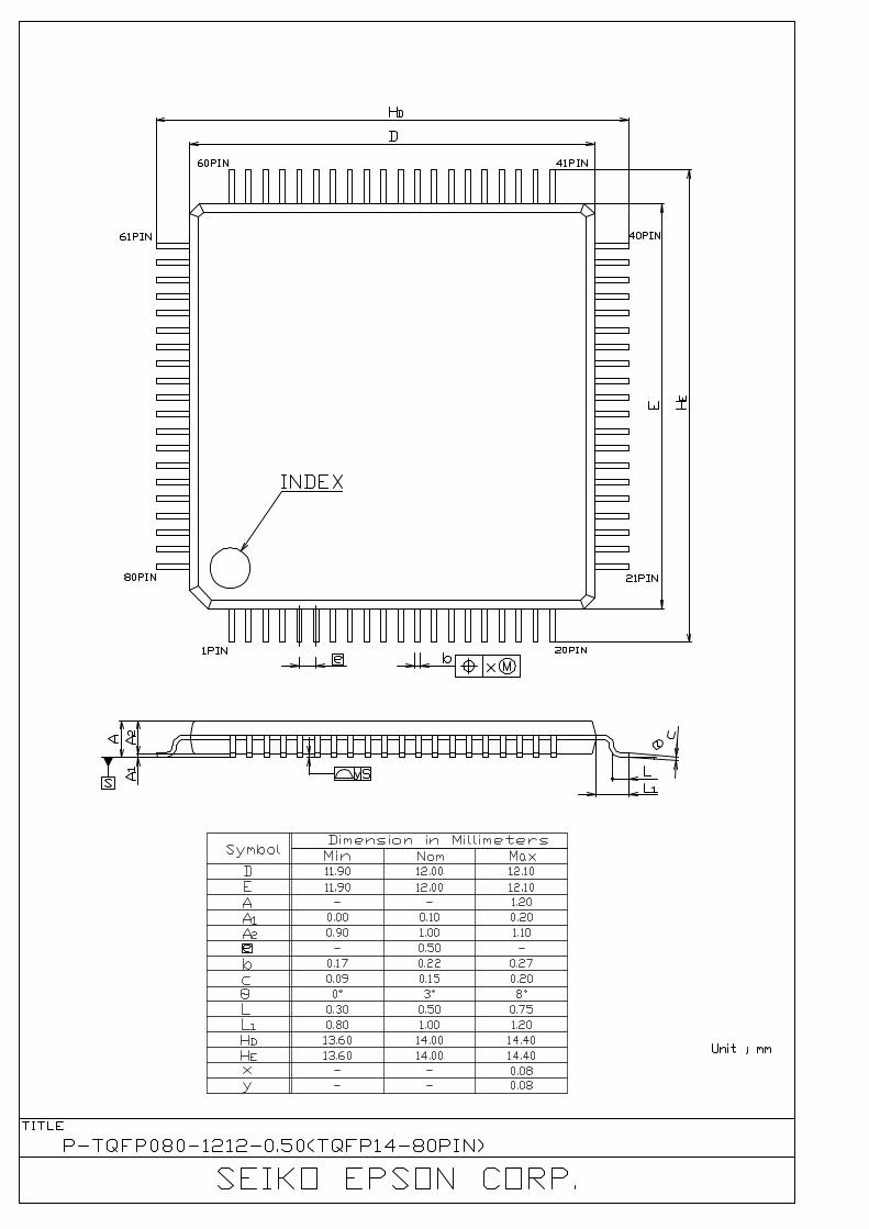
Shipping form 1 TQFP12-48 ( 7mm x 7mm, 0.5mm pitch) 2 QFP13-64 (10mm x 10mm, 0.5mm pitch) 3 TQFP14-80 (12mm x 12mm, 0.5mm pitch) 4 QFP15-100 (14mm x 14mm, 0.5mm pitch)
*1 SLEEP mode refers to deep sleep mode in the Cortex®-M0+ processor. *2 HALT mode refers to sleep mode in the Cortex®-M0+ processor.
■ Block Diagram
CPU core, Interrupt controller, and debugger
(Cortex®-M0+) SWCLK
SWD
32-b
it AH
B bu
s
Flash memory 192K bytes
MTB RAM 8K bytes
DMA controller 4 Ch.
Synchronous serial interface
(SPIA) 3 Ch. I2C
(I2C) 3 Ch.
HW Processor
I/O port01 (PPORT)
Watchdog timer
(WDT2) Real-time clock
(RTCA) Supply voltage
detector (SVD3) 1 Ch. 16-bit timer (T16) 8Ch.
16-bit PWM timer
(T16B) 2 Ch.
UART (UART3) 3 Ch.
Clock generator (CLG)
IOSC oscillator
OSC1 oscillator
OSC3 oscillator
EXOSC oscillator
System reset controller
(SRC) Power-on reset/ Brown-out reset
(POR/BOR)
Power generator (PWGA)
System clock
Interrupt
DMA request
Cache controller
Cache RAM 512 bytes
12bit A/D convertor
(ADC12A) 1 Ch. ADIN00-07
I/O port23 (PPORT)
I/O portOthers (PPORT)
VREFA0
#RESET
EXCL00-01 CAP10-13
SOUNDO_P SOUNDO_N
P00-07 P10-17
#ADTRG
QSDIO00-03 QSPICLK0 #QSPISS0 SDI0-2 SDO0-2 SPICLK0-2
USIN0-2
#SPISS0-2 SDA0-2 SCL0-2
USOUT0-2
P20-27 P30-37 P40-47 P50-57 P60-67 P70-77 P80-87 P90-95 PA0-A6
VDD VSS
VDDQSPI
VPP
RAM 14K bytes
Sound_DAC 1 Ch.
EXSVD0-1
IR remote controller
(REMC2) 1Ch. REMO CLPLS
EXCL10-11 R/F converter
(RFC) 1 Ch. SENB0 REF0 EFCLKO0
RFIN0 SENA0
TOUT10-13
Quad synchronous
serial interface (QSPI) 1 Ch.
CAP00-03 TOUT00-03
16-bit peripheral bus
S1C31D50
4
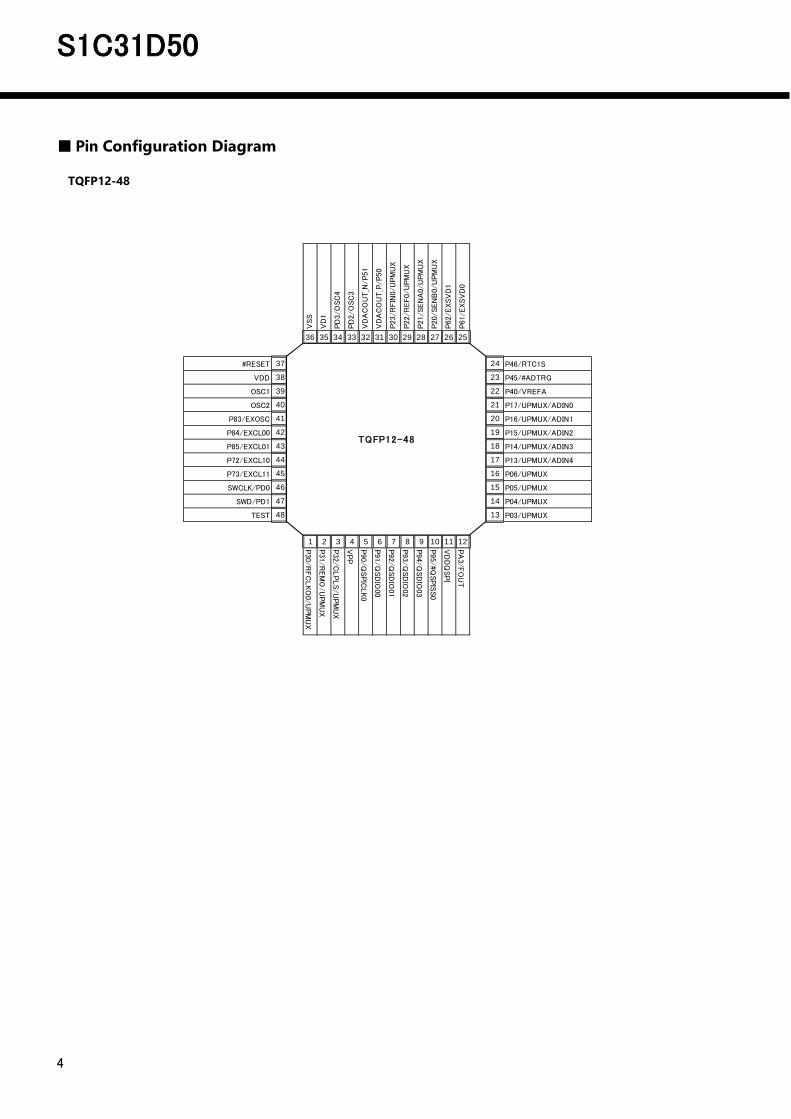
■ Pin Configuration Diagram
TQFP12-48
VSS
VD
1
PD
3/O
SC
4
PD
2/O
SC
3
VD
AC
OU
T_N
/P51
VD
AC
OU
T_P
/P50
P23
/RFIN
0/U
PM
UX
P22
/REF0/
UPM
UX
P21
/SEN
A0/
UPM
UX
P20
/SEN
B0/
UPM
UX
P62
/EXSV
D1
P61
/EXSV
D0
36 35 34 33 32 31 30 29 28 27 26 25
#RESET 37 24 P46/RTC1S
VDD 38 23 P45/#ADTRG
OSC1 39 22 P40/VREFA
OSC2 40 21 P17/UPMUX/ADIN0
P83/EXOSC 41 20 P16/UPMUX/ADIN1
P84/EXCL00 42 19 P15/UPMUX/ADIN2
P85/EXCL01 43 18 P14/UPMUX/ADIN3
P72/EXCL10 44 17 P13/UPMUX/ADIN4
P73/EXCL11 45 16 P06/UPMUX
SWCLK/PD0 46 15 P05/UPMUX
SWD/PD1 47 14 P04/UPMUX
TEST 48 13 P03/UPMUX
1 2 3 4 5 6 7 8 9 10 11 12
P30/R
FC
LKO
0/UPM
UX
P31/R
EM
O/U
PM
UX
P32/C
LPLS/U
PM
UX
VPP
P90/Q
SPIC
LK0
P91/Q
SD
IO00
P92/Q
SD
IO01
P93/Q
SD
IO02
P94/Q
SD
IO03
P95/#Q
SPIS
S0
VD
DQ
SPI
PA
3/FO
UT
TQFP12-48

S1C31D50
QFP13-64
VSS
VD
1
PD
3/O
SC
4
PD
2/O
SC
3
VD
AC
OU
T_N
/P51
VD
AC
OU
T_P
/P50
P27
/UPM
UX
P26
/UPM
UX
P25
/UPM
UX
P24
/UPM
UX
P23
/RFIN
0/U
PM
UX
P22
/REF0/
UPM
UX
P21
/SEN
A0/
UPM
UX
P20
/SEN
B0/
UPM
UX
P62
/EXSV
D1
P61
/EXSV
D0
48 47 46 45 44 43 42 41 40 39 38 37 36 35 34 33
#RESET 49 32 P46/RTC1S
VDD 50 31 P45/#ADTRG
OSC1 51 30 P44
OSC2 52 29 P43
P81 53 28 P40/VREFA
P82 54 27 P17/UPMUX/ADIN0
P83/EXOSC 55 26 P16/UPMUX/ADIN1
P84/EXCL00 56 25 P15/UPMUX/ADIN2
P85/EXCL01 57 24 P14/UPMUX/ADIN3
P70 58 23 P13/UPMUX/ADIN4
P71 59 22 P12/UPMUX/ADIN5
P72/EXCL10 60 21 P11/UPMUX/ADIN6
P73/EXCL11 61 20 P06/UPMUX
SWCLK/PD0 62 19 P05/UPMUX
SWD/PD1 63 18 P04/UPMUX
TEST 64 17 P03/UPMUX
1 2 3 4 5 6 7 8 9 10 11 12 13 14 15 16
P30/R
FC
LKO
0/UPM
UX
P31/R
EM
O/U
PM
UX
P32/C
LPLS/U
PM
UX
P33/U
PM
UX
P34/U
PM
UX
VPP
P90/Q
SPIC
LK0
P91/Q
SD
IO00
P92/Q
SD
IO01
P93/Q
SD
IO02
P94/Q
SD
IO03
P95/#Q
SPIS
S0
VD
DQ
SPI
PA
1
PA
2
PA
3/FO
UT
QFP13-64

S1C31D50
6
TQFP14-80pin
VSS
VD
1
PD
3/O
SC
4
PD
2/O
SC
3
P53
P52
VD
AC
OU
T_N
/P51
VD
AC
OU
T_P
/P50
P27/U
PM
UX
P26/U
PM
UX
P25/U
PM
UX
P24/U
PM
UX
P23/R
FIN
0/U
PM
UX
P22/R
EF0/U
PM
UX
P21/SEN
A0/U
PM
UX
P20/SEN
B0/U
PM
UX
P64
P63
P62/EXSV
D1
P61/EXSV
D0
60 59 58 57 56 55 54 53 52 51 50 49 48 47 46 45 44 43 42 41
#RESET 61 40 P46/RTC1S
VDD 62 39 P45/#ADTRG
OSC1 63 38 P44
OSC2 64 37 P43
P80 65 36 P42
P81 66 35 P41
P82 67 34 P40/VREFA
P83/EXOSC 68 33 P17/UPMUX/ADIN0
P84/EXCL00 69 32 P16/UPMUX/ADIN1
P85/EXCL01 70 31 P15/UPMUX/ADIN2
P86 71 30 P14/UPMUX/ADIN3
P87 72 29 P13/UPMUX/ADIN4
P70 73 28 P12/UPMUX/ADIN5
P71 74 27 P11/UPMUX/ADIN6
P72/EXCL10 75 26 P10/UPMUX/ADIN7
P73/EXCL11 76 25 P07/UPMUX
P74 77 24 P06/UPMUX
SWCLK/PD0 78 23 P05/UPMUX
SWD/PD1 79 22 P04/UPMUX
TEST 80 21 P03/UPMUX
1 2 3 4 5 6 7 8 9 10 11 12 13 14 15 16 17 18 19 20
PD
4
P30/R
FC
LKO
0/U
PM
UX
P31/R
EM
O/U
PM
UX
P32/C
LPLS/U
PM
UX
P33/U
PM
UX
P34/U
PM
UX
P35/U
PM
UX
VPP
P90/Q
SPIC
LK0
P91/Q
SD
IO00
P92/Q
SD
IO01
P93/Q
SD
IO02
P94/Q
SD
IO03
P95/#Q
SPIS
S0
VD
DQ
SPI
PA
0
PA
1
PA
2
PA
3/FO
UT
PA
4
TQFP14-80
S1C31D50
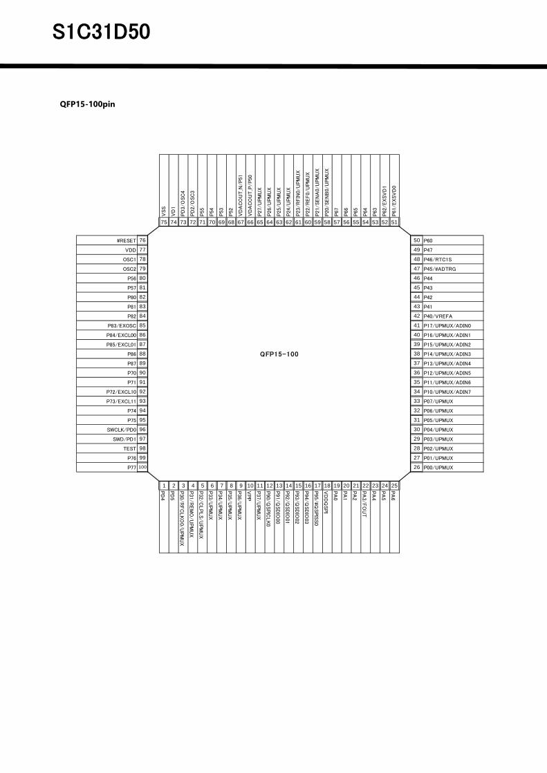
QFP15-100pin
V
SS
VD
1
PD
3/O
SC
4
PD
2/O
SC
3
P55
P54
P53
P52
VD
AC
OU
T_N
/P51
VD
AC
OU
T_P
/P50
P27
/UPM
UX
P26
/UPM
UX
P25
/UPM
UX
P24
/UPM
UX
P23
/RFIN
0/U
PM
UX
P22
/REF0/
UPM
UX
P21
/SEN
A0/
UPM
UX
P20
/SEN
B0/
UPM
UX
P67
P66
P65
P64
P63
P62
/EXSV
D1
P61
/EXSV
D0
75 74 73 72 71 70 69 68 67 66 65 64 63 62 61 60 59 58 57 56 55 54 53 52 51
#RESET 76 50 P60
VDD 77 49 P47
OSC1 78 48 P46/RTC1S
OSC2 79 47 P45/#ADTRG
P56 80 46 P44
P57 81 45 P43
P80 82 44 P42
P81 83 43 P41
P82 84 42 P40/VREFA
P83/EXOSC 85 41 P17/UPMUX/ADIN0
P84/EXCL00 86 40 P16/UPMUX/ADIN1
P85/EXCL01 87 39 P15/UPMUX/ADIN2
P86 88 38 P14/UPMUX/ADIN3
P87 89 37 P13/UPMUX/ADIN4
P70 90 36 P12/UPMUX/ADIN5
P71 91 35 P11/UPMUX/ADIN6
P72/EXCL10 92 34 P10/UPMUX/ADIN7
P73/EXCL11 93 33 P07/UPMUX
P74 94 32 P06/UPMUX
P75 95 31 P05/UPMUX
SWCLK/PD0 96 30 P04/UPMUX
SWD/PD1 97 29 P03/UPMUX
TEST 98 28 P02/UPMUX
P76 99 27 P01/UPMUX
P77 100 26 P00/UPMUX
1 2 3 4 5 6 7 8 9 10 11 12 13 14 15 16 17 18 19 20 21 22 23 24 25
PD
4
PD
5
P30/R
FC
LKO
0/UPM
UX
P31/R
EM
O/U
PM
UX
P32/C
LPLS/U
PM
UX
P33/U
PM
UX
P34/U
PM
UX
P35/U
PM
UX
P36/U
PM
UX
VPP
P37/U
PM
UX
P90/Q
SPIC
LK0
P91/Q
SD
IO00
P92/Q
SD
IO01
P93/Q
SD
IO02
P94/Q
SD
IO03
P95/#Q
SPIS
S0
VD
DQ
SPI
PA
0
PA
1
PA
2
PA
3/FO
UT
PA
4
PA
5
PA
6
QFP15-100

S1C31D50
8
■ Pin Descriptions Symbol meanings
Assigned signal: The signal listed at the top of each pin is assigned in the initial state. The pin function must be switched via software to assign another signal (see the “I/O Ports” chapter).
I/O: I = Input O = Output I/O = Input/output P = Power supply A = Analog signal Hi-Z = High impedance state
Initial state: I (Pull-up) = Input with pulled up I (Pull-down) = Input with pulled down Hi-Z = High impedance state O (H) = High level output O (L) = Low level output
Tolerant fail-safe structure: ✓ = Over voltage tolerant fail-safe type I/O cell included
Pin name Pin function I/O Initial Tolerant fail-safe structure
Description
VDD VDD P - - Power(+) VSS VSS P - - GND VPP VPP P - - Flash Programing Power VD1 VD1 A - - VDDQSPI VDDQSPI P - - SPI Flash interface voltage supply. OSC1 OSC1 A - - OSC1 oscillator input OSC2 OSC2 A - - OSC1 oscillator output TEST TEST I I(Pull-down) - Test mode enable #RESET #RESET I I(Pull-up) - Reset input P00 P00 I/O Hi-Z ✓ I/O port – – UPMUX UPMUX – – P01 P01 I/O Hi-Z ✓ I/O port – – UPMUX UPMUX – – P02 P02 I/O Hi-Z ✓ I/O port – – UPMUX UPMUX – – P03 P03 I/O Hi-Z ✓ I/O port – – UPMUX UPMUX – – P04 P04 I/O Hi-Z ✓ I/O port – – UPMUX UPMUX – – P05 P05 I/O Hi-Z ✓ I/O port – – UPMUX UPMUX – – P06 P06 I/O Hi-Z ✓ I/O port – – UPMUX UPMUX – –

S1C31D50
P07 P07 I/O Hi-Z ✓ I/O port – – UPMUX UPMUX – – P10 P10 I/O Hi-Z - I/O port – – UPMUX UPMUX ADIN7 ADC ch.0 P11 P11 I/O Hi-Z - I/O port – – UPMUX UPMUX ADIN6 ADC ch.0 P12 P12 I/O Hi-Z - I/O port – – UPMUX UPMUX ADIN5 ADC ch.0 P13 P13 I/O Hi-Z - I/O port – – UPMUX UPMUX ADIN4 ADC ch.0 P14 P14 I/O Hi-Z - I/O port – – UPMUX UPMUX ADIN3 ADC ch.0 P15 P15 I/O Hi-Z - I/O port – – UPMUX UPMUX ADIN2 ADC ch.0 P16 P16 I/O Hi-Z - I/O port – – UPMUX UPMUX ADIN1 ADC ch.0 P17 P17 I/O Hi-Z - I/O port – – UPMUX UPMUX ADIN0 ADC ch.0 P20 P20 I/O Hi-Z ✓ I/O port SENB0 RFC UPMUX UPMUX – – P21 P21 I/O Hi-Z ✓ I/O port SENA0 RFC UPMUX UPMUX – – P22 P22 I/O Hi-Z ✓ I/O port REF0 RFC UPMUX UPMUX – – P23 P23 I/O Hi-Z ✓ I/O port RFIN0 RFC UPMUX UPMUX - - P24 P24 I/O Hi-Z ✓ I/O port - - UPMUX UPMUX – – P25 P25 I/O Hi-Z ✓ I/O port - - UPMUX UPMUX - -

S1C31D50
10
P26 P26 I/O Hi-Z ✓ I/O port – – UPMUX UPMUX – – P27 P27 I/O Hi-Z ✓ I/O port – – UPMUX UPMUX – – P30 P30 I/O Hi-Z ✓ I/O port RFCLKO0 RFC UPMUX UPMUX – – P31 P31 I/O Hi-Z ✓ I/O port REMO REMC2 UPMUX UPMUX – – P32 P32 I/O Hi-Z ✓ I/O port CLPLS REMC2 UPMUX UPMUX – – P33 P33 I/O Hi-Z ✓ I/O port – – UPMUX UPMUX – – P34 P34 I/O Hi-Z ✓ I/O port – – UPMUX UPMUX – – P35 P35 I/O Hi-Z ✓ I/O port – – UPMUX UPMUX – – P36 P36 I/O Hi-Z ✓ I/O port – – UPMUX UPMUX – – P37 P37 I/O Hi-Z ✓ I/O port – – UPMUX UPMUX – – P40 P40 I/O Hi-Z - I/O port – – – – VREFA ADC ch.0 P41 P41 I/O Hi-Z ✓ I/O port – – – – – – P42 P42 I/O Hi-Z ✓ I/O port – – – – – – P43 P43 I/O Hi-Z ✓ I/O port – – – – – – P44 P44 I/O Hi-Z ✓ I/O port – – – – – –

S1C31D50
P45 P45 I/O Hi-Z ✓ I/O port #ADTRG ADC – – – – P46 P46 I/O Hi-Z ✓ I/O port RTC1S RTCA – – – – P47 P47 I/O Hi-Z ✓ I/O port – – – – – – P50 VDACOUT_P I/O O(L) ✓ VDAC(default) P50 I/O port – – – – P51 VDACOUT_N I/O O(L) ✓ VDAC(default) P51 I/O port – – – – P52 P52 I/O Hi-Z ✓ I/O port – – – – – – P53 P53 I/O Hi-Z ✓ I/O port – – – – – – P54 P54 I/O Hi-Z ✓ I/O port – – – – – – P55 P55 I/O Hi-Z ✓ I/O port – – – – – – P56 P56 I/O Hi-Z ✓ I/O port – – – – – – P57 P57 I/O Hi-Z ✓ I/O port – – – – – – P60 P60 I/O Hi-Z ✓ I/O port – – – – – – P61 P61 I/O Hi-Z ✓ I/O port – – – – EXSVD0 SVD3 Ch.0 P62 P62 I/O Hi-Z ✓ I/O port – – – – EXSVD1 SVD3 Ch.0 P63 P63 I/O Hi-Z ✓ I/O port – – – – – –

S1C31D50
12
P64 P64 I/O Hi-Z ✓ I/O port – – – – – – P65 P65 I/O Hi-Z ✓ I/O port – – – – – – P66 P66 I/O Hi-Z ✓ I/O port – – – – – – P67 P67 I/O Hi-Z ✓ I/O port – – – – – – P70 P70 I/O Hi-Z ✓ I/O port – – – – – – P71 P71 I/O Hi-Z ✓ I/O port – – – – – – P72 P72 I/O Hi-Z ✓ I/O port EXCL10 T16B Ch.1 – – – – P73 P73 I/O Hi-Z ✓ I/O port EXCL11 T16B Ch.1 – – – – P74 P74 I/O Hi-Z ✓ I/O port – – – – – – P75 P75 I/O Hi-Z ✓ I/O port – – – – – – P76 P76 I/O Hi-Z ✓ I/O port – – – – – – P77 P77 I/O Hi-Z ✓ I/O port – – – – – – P80 P80 I/O Hi-Z ✓ I/O port – – – – – – P81 P81 I/O Hi-Z ✓ I/O port – – – – – – P82 P82 I/O Hi-Z ✓ I/O port – – – – – –

S1C31D50
P83 P83 I/O Hi-Z ✓ I/O port EXOSC CLG – – – – P84 P84 I/O Hi-Z ✓ I/O port EXCL00 T16B Ch.0 – – – – P85 P85 I/O Hi-Z ✓ I/O port EXCL01 T16B Ch.0 – – – – P86 P86 I/O Hi-Z ✓ I/O port – – – – – – P87 P87 I/O Hi-Z ✓ I/O port – – – – – – P90 P90 I/O Hi-Z ✓ I/O port QSPICLK0 QSPI Ch.0 – – – – P91 P91 I/O Hi-Z ✓ I/O port QSDIO00 QSPI Ch.0 – – – – P92 P92 I/O Hi-Z ✓ I/O port QSDIO01 QSPI Ch.0 – – – – P93 P93 I/O Hi-Z ✓ I/O port QSDIO02 QSPI Ch.0 – – – – P94 P94 I/O Hi-Z ✓ I/O port QSDIO03 QSPI Ch.0 – – – – P95 P95 I/O Hi-Z ✓ I/O port #QSPISS0 QSPI Ch.0 – – – – PA0 PA0 I/O Hi-Z ✓ I/O port – – – – – – PA1 PA1 I/O Hi-Z ✓ I/O port – – – – – – PA2 PA2 I/O Hi-Z ✓ I/O port – – – – – – PA3 PA3 I/O Hi-Z ✓ I/O port FOUT CLG – – – –

S1C31D50
14
PA4 PA4 I/O Hi-Z ✓ I/O port – – – – – – PA5 PA5 I/O Hi-Z ✓ I/O port – – – – – – PA6 PA6 I/O Hi-Z ✓ I/O port – – – – – – PD0 SWCLK I/O (Pull-up) ✓ DBG(default) PD0 I/O port – – – – PD1 SWD I/O (Pull-up) ✓ DBG(default) PD1 I/O port – – – – PD2 PD2 I/O Hi-Z - I/O port – – – – OSC3 CLG PD3 PD3 I/O Hi-Z - I/O port – – – – OSC4 CLG PD4 PD4 I/O Hi-Z ✓ I/O port – – – – – – PD5 PD5 I/O Hi-Z ✓ I/O port – – – – – – Note:
In the peripheral circuit descriptions, the assigned signal name is used as the pin name.
Universal port multiplexer (UPMUX) The universal port multiplexer (UPMUX) allows software to select the peripheral circuit input/output function to be assigned to each pin from those listed below.
Table 1.3.3.2 Peripheral Circuit Input/output Function Selectable by UPMUX Peripheral Signal I/O Ch.No. Function
I2C SCLn I/O n=0,1,2 - I2C Ch.n clock input/output SDAn I/O - I2C Ch.n data input/output UART USINn I n=0,1,2 - UART Ch,n data input USOUTn O - UART Ch,n data output SPI SDIn I n=0,1,2 - SPIA ch.n data input SDOn O - SPIA ch.n data output SPICLKn I/O - SPIA Ch.n clock input/output #SPISSn I - SPIA Ch.n slave-select input PWM timer TOUTn0/CAPn0 I/O n=0,1 - 16-bit PWM timer Ch.n PWM output / caputure input 0 TOUTn1/CAPn1 I/O - 16-bit PWM timer Ch.n PWM output / caputure input 1 TOUTn2/CAPn2 I/O - 16-bit PWM timer Ch.n PWM output / caputure input 2 TOUTn3/CAPn3 I/O - 16-bit PWM timer Ch.n PWM output / caputure input 3
Note: Do not assign a function to two or more pins simultaneously.

S1C31D50
Pin Details
QFP15 -100
TQFP14 -80
QFP13 -64
TQFP12 -48
Pin. No
Pin. No
Pin. No
Pin. No Pin Name Function
1 1 ― ― PD4 PD4 2 ― ― ― PD5 PD5 3 2 1 1 P30 P30/RFCLKO0/UPMUX 4 3 2 2 P31 P31/REMO/UPMUX 5 4 3 3 P32 P32/CLPLS/UPMUX 6 5 4 ― P33 P33/UPMUX 7 6 5 ― P34 P34/UPMUX 8 7 ― ― P35 P35/UPMUX 9 ― ― ― P36 P36/UPMUX 10 8 6 4 VPP VPP 11 ― ― ― P37 P37/UPMUX 12 9 7 5 P90 P90/QSPICLK0 13 10 8 6 P91 P91/QSDIO00 14 11 9 7 P92 P92/QSDIO01 15 12 10 8 P93 P93/QSDIO02 16 13 11 9 P94 P94/QSDIO03 17 14 12 10 P95 P95/#QSPISS0 18 15 13 11 VDDQSPI VDDQSPI 19 16 ― ― PA0 PA0 20 17 14 ― PA1 PA1 21 18 15 ― PA2 PA2 22 19 16 12 PA3 PA3/FOUT 23 20 ― ― PA4 PA4 24 ― ― ― PA5 PA5 25 ― ― ― PA6 PA6 26 ― ― ― P00 P00/UPMUX 27 ― ― ― P01 P01/UPMUX 28 ― ― ― P02 P02/UPMUX 29 21 17 13 P03 P03/UPMUX 30 22 18 14 P04 P04/UPMUX 31 23 19 15 P05 P05/UPMUX 32 24 20 16 P06 P06/UPMUX 33 25 ― ― P07 P07UPMUX 34 26 ― ― P10 P10/UPMUX/ADIN7 35 27 21 ― P11 P11/UPMUX/ADIN6 36 28 22 ― P12 P12/UPMUX/ADIN5 37 29 23 17 P13 P13/UPMUX/ADIN4 38 30 24 18 P14 P14/UPMUX/ADIN3 39 31 25 19 P15 P15/UPMUX/ADIN2 40 32 26 20 P16 P16/UPMUX/ADIN1 41 33 27 21 P17 P17/UPMUX/ADIN0 42 34 28 22 P40 P40/VREFA 43 35 ― ― P41 P41 44 36 ― ― P42 P42 45 37 29 ― P43 P43 46 38 30 ― P44 P44 47 39 31 23 P45 P45/#ADTRG 48 40 32 24 P46 P46/RTC1S 49 ― ― ― P47 P47 50 ― ― ― P60 P60 51 41 33 25 P61 P61/EXSVD0 52 42 34 26 P62 P62/EXSVD1 53 43 ― ― P63 P63 54 44 ― ― P64 P64 55 ― ― ― P65 P65 56 ― ― ― P66 P66

S1C31D50
16
57 ― ― ― P67 P67 58 45 35 27 P20 P20/SENB0/UPMUX 59 46 36 28 P21 P21/SENA0/UPMUX 60 47 37 29 P22 P22/REF0/UPMUX 61 48 38 30 P23 P23/RFIN0/UPMUX 62 49 39 ― P24 P24/UPMUX 63 50 40 ― P25 P25/UPMUX 64 51 41 ― P26 P26/UPMUX 65 52 42 ― P27 P27/UPMUX 66 53 43 31 P50 P50/VDACOUT_P 67 54 44 32 P51 P51/VDACOUT_N 68 55 ― ― P52 P52 69 56 ― ― P53 P53 70 ― ― ― P54 P54 71 ― ― ― P55 P55 72 57 45 33 PD2 PD2/OCS3 73 58 46 34 PD3 PD3/OSC4 74 59 47 35 VD1 VD1 75 60 48 36 VSS VSS 76 61 49 37 #RESET #RESET 77 62 50 38 VDD VDD 78 63 51 39 OSC1 OSC1 79 64 52 40 OSC2 OSC2 80 ― ― ― P56 P56 81 ― ― ― P57 P57 82 65 ― ― P80 P80 83 66 53 ― P81 P81 84 67 54 ― P82 P82 85 68 55 41 P83 P83/EXOSC 86 69 56 42 P84 P84/EXCL00 87 70 57 43 P85 P85/EXCL01 88 71 ― ― P86 P86 89 72 ― ― P87 P87 90 73 58 ― P70 P70 91 74 59 ― P71 P71 92 75 60 44 P72 P72/EXCL10 93 76 61 45 P73 P73/EXCL11 94 77 ― ― P74 P74 95 ― ― ― P75 P75 96 78 62 46 PD0 PD0/SWCLK 97 79 63 47 PD1 PD1/SWD 98 80 64 48 TEST TEST 99 ― ― ― P76 P76 100 ― ― ― P77 P77

S1C31D50
■ EPSON Voice Creation PC Tool
EPSON Voice creation PC tool makes voice related development easy because of no-studio recording, no narrator arrangement. This tool supports English, Chinese, Japanese and Korean(all female voice), and easily creation, modification can be done, by “wav file” import function, existing wav file can be used.
Input Text Import wav fileAdjust pronunciation Alignment Create Sound ROM
Just push the button to create Sound ROM

S1C31D50
18
■ Basic External Connection Diagram
Single Connection to AMP
Differential Connection to AMP
Enable IN-
IN+
VDACOUT_P
PORT Enable Control
Cin Rin
39uF
510Ω
39uF
510Ω
Low Pass Filter: cutoff 8kHz
Enable IN-
IN+
VDACOUT_P
PORT Enable Control
VDACOUT_N
Low Pass Filter: cutoff 8kHz
Cin Rin
39uF
510Ω
39uF
510Ω
Cin Rin
39uF
510Ω
39uF
510Ω
VDD
VD1
VSS
VDDQSPI
OSC1 OSC2
OSC3 OSC4
#RESET TEST
EXSVDn
REMO
Pxy
External voltage
IR transmitter module
I/O SDIn
SDOn SPICLKn #SPISSn
SPI
QSDIO00 QSDIO01 QSDIO02 QSDIO03
QSPICLK0 #QSPISS0
QSPI
USINn USOUTn
SCLn SDAn I2C
UART
TOUTn0/CAPn0 : :
TOUTn3/CAPn3 PWM/Captur
ADIN00-07 #ADTRG0
VREFA0
A/D conversion inputs CVREFA
SWCLK SWD VPP
VDD
Debugging tool
S1C31D50
VDACOUT_P VDACOUT_N VOICE/AUDIO


S1C31D50
■ Revision History
Revision details Date Rev. Page Type Details
2018/7/30 1.00 All New New release
SALES & MARKETING DIVISION
Device Sales & Marketing Department 421-8 Hino, Hino-shi, Tokyo 191-8501, JAPAN
Phone: +81-42-587-5814 FAX: +81-42-587-5116 Document code: 413699100 First issue July, 2018
NOTICE:
No part of this material may be reproduced or duplicated in any form or by any means without the written permission of Seiko Epson. Seiko Epson
reserves the right to make changes to this material without notice. Seiko Epson does not assume any liability of any kind arising out of any
inaccuracies contained in this material or due to its application or use in any product or circuit and, further, there is no representation that this
material is applicable to products requiring high level reliability, such as, medical products. Moreover, no license to any intellectual property rights is
granted by implication or otherwise, and there is no representation or warranty that anything made in accordance with this material will be free from
any patent or copyright infringement of a third party. When exporting the products or technology described in this material, you should comply with the
applicable export control laws and regulations and follow the procedures required by such laws and regulations. You are requested not to use, to resell,
to export and/or to otherwise dispose of the products (and any technical information furnished, if any) for the development and/or manufacture of
weapon of mass destruction or for other military purposes.
ARM and Cortex are registered trademarks of ARM Limited (or its subsidiaries) in the EU and/or elsewhere. All rights reserved.
All brands or product names mentioned herein are trademarks and/or registered trademarks of their respective companies.
Seiko Epson Corporation 2018, All rights reserved
global.epson.com/products_and_drivers/semicon/