Embed Size (px)
Citation preview

UPTEC F10 020
Examensarbete 30 hpMars 2010
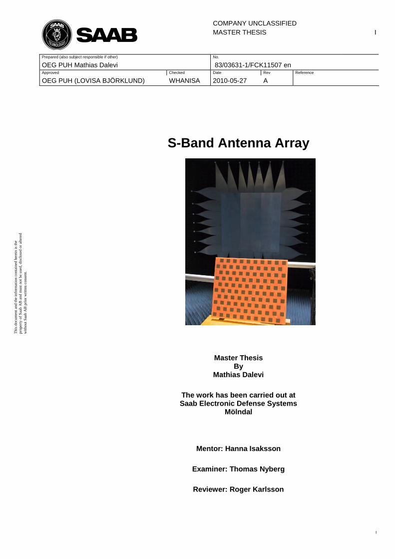
S-Band Antenna Array
Mathias Dalevi
Teknisk- naturvetenskaplig fakultet UTH-enheten Besöksadress: Ångströmlaboratoriet Lägerhyddsvägen 1 Hus 4, Plan 0 Postadress: Box 536 751 21 Uppsala Telefon: 018 – 471 30 03 Telefax: 018 – 471 30 00 Hemsida: http://www.teknat.uu.se/student
Abstract
S-Band Antenna Array
Mathias Dalevi
This report presents concepts for a planar active electronically scannedantenna(AESA). The goal of the project was to devlop a low-weight, low profile, thin,S-band antenna with wide-scan angle capabilities. In the final concept the serviceaspects of the T/R-modules was also taken into acount in order to allow easy and fastreplacements of these components. The antenna was designed and optimised usingthe commercial software Ansoft HFSS. A prototype of the antenna was constructedand later measured and verified. The final concept is a 2m×2m antenna with anestimated weight of around 320 kg, around 11 cm thick (where the thickness of theantenna element is 1.76 cm) and has a maximum scan angle range of more than 45degrees (with <–10dB active reflection) in the frequency band 3–3.5 GHz.
Sponsor: Saab Electronic Defense SystemsISSN: 1401-5757, UPTEC F10 020Examinator: Thomas NybergÄmnesgranskare: Roger KarlssonHandledare: Hanna Isaksson
COMPANY UNCLASSIFIED
MASTER THESIS
I
Prepared (also subject responsible if other) No.
OEG PUH Mathias Dalevi 83/03631-1/FCK11507 en Approved Checked Date Rev Reference
OEG PUH (LOVISA BJÖRKLUND) WHANISA 2010-05-27 A
I
This
docu
men
t an
d t
he
info
rmat
ion c
onta
ined
her
ein i
s th
e
pro
per
ty o
f S
aab A
B a
nd m
ust
not
be
use
d,
dis
close
d o
r al
tere
d
wit
hout
Saa
b A
B p
rior
wri
tten
conse
nt.
S-Band Antenna Array
Master Thesis By
Mathias Dalevi
The work has been carried out at Saab Electronic Defense Systems
Mölndal
Mentor: Hanna Isaksson
Examiner: Thomas Nyberg
Reviewer: Roger Karlsson
COMPANY UNCLASSIFIED
MASTER THESIS
II
Prepared (also subject responsible if other) No.
OEG PUH Mathias Dalevi 83/03631-1/FCK11507 en Approved Checked Date Rev Reference
OEG PUH (LOVISA BJÖRKLUND) WHANISA 2010-05-27 A
II
This
docu
men
t an
d t
he
info
rmat
ion c
onta
ined
her
ein i
s th
e
pro
per
ty o
f S
aab A
B a
nd m
ust
not
be
use
d,
dis
close
d o
r al
tere
d
wit
hout
Saa
b A
B p
rior
wri
tten
conse
nt.
COMPANY UNCLASSIFIED
MASTER THESIS
III
Prepared (also subject responsible if other) No.
OEG PUH Mathias Dalevi 83/03631-1/FCK11507 en Approved Checked Date Rev Reference
OEG PUH (LOVISA BJÖRKLUND) WHANISA 2010-05-27 A
III
This
docu
men
t an
d t
he
info
rmat
ion c
onta
ined
her
ein i
s th
e
pro
per
ty o
f S
aab A
B a
nd m
ust
not
be
use
d,
dis
close
d o
r al
tere
d
wit
hout
Saa
b A
B p
rior
wri
tten
conse
nt.
Abstract
This report presents concepts for a planar active electronically scanned
antenna(AESA). The goal of the project was to devlop a low-weight, low
profile, thin, S-band antenna with wide-scan angle capabilities. In the final
concept the service aspects of the T/R-modules was also taken into acount in
order to allow easy and fast replacements of these components. The antenna
was designed and optimised using the commercial software Ansoft HFSS. A
prototype of the antenna was constructed and later measured and verified. The
final concept is a 2m×2m antenna with an estimated weight of around 320 kg,
around 11 cm thick (where the thickness of the antenna element is 1.76 cm)
and has a maximum scan angle range of more than 45 degrees (with <–10dB
active reflection) in the frequency band 3–3.5 GHz.
COMPANY UNCLASSIFIED
MASTER THESIS
IV
Prepared (also subject responsible if other) No.
OEG PUH Mathias Dalevi 83/03631-1/FCK11507 en Approved Checked Date Rev Reference
OEG PUH (LOVISA BJÖRKLUND) WHANISA 2010-05-27 A
IV
This
docu
men
t an
d t
he
info
rmat
ion c
onta
ined
her
ein i
s th
e
pro
per
ty o
f S
aab A
B a
nd m
ust
not
be
use
d,
dis
close
d o
r al
tere
d
wit
hout
Saa
b A
B p
rior
wri
tten
conse
nt.
Populärvetenskaplig Sammanfattning
Det här arbetet presenterar koncept för en aktiv elektronisk styrd
antenn(AESA). Arbetet är ett sammarbete mellan två examenarbeten,
elektriska och mekaniska koncept, där de elektriska koncepten innefattar
framtagning och optimering av antennelementen. Målet med projektet var att
ta fram en plan, lätt och tunn AESA med stora utstyrningsmöjligheter i S-
bandet mellan 3–3.5 GHz.
En AESA har många fördelar jämfört med en konventionell mekaniskt styrd
antenn eftersom den kan rikta in loben elektriskt och därmed snabbare scanna
av ett område. Detta är möjligt eftersom varje antennelement styrs av sin egen
T/R-modul (sändar/mottagar-modul). Loben styrs genom att individuellt
kontrollera fasen av strömmen på varje antennelement. Det går även att
kontrollera amplituden av strömmen vid varje antennelement vilket ger
möjigheter som att motverka störningar, få mindre sidlober eller en smalare
respektive bredare lob mm. Att varje element styrs av sin egen modul gör även
systemet mer pålitligt eftersom det fortfarande skulle fungera trots att en
sändar/mottagar-modul gått sönder.
Arbetet inleddes med en litteraturstudie där olika koncept undersöktes och
utvärderades för att sedan gå vidare med det mest lovande konceptet som var
en aperture kopplad stackad patch. Antennelementet designades och
optimerades med EM-simulatorprogrammet Ansoft HFSS v11.2 där elementet
realiserades med periodiska randvillkor och optimerades med en olinjär
programmeringsmetod. Efter optimeringen konstruerades en prototyp av
antennen bestående av 10×10 element som sedan verifierades och testades.
Resultatet av det simulerade antennelementet visar utstyrningsmöjligheter på
mer än 45 grader i varje plan med reflektioner på mindre än –10dB i bandet
mellan 3–3.5 GHz. De uppmätta resultaten på prototypen skiljer sig något från
de simulerade resultaten på prototypen och visar en något bättre prestanda.

COMPANY UNCLASSIFIED
MASTER THESIS
V
Prepared (also subject responsible if other) No.
OEG PUH Mathias Dalevi 83/03631-1/FCK11507 en Approved Checked Date Rev Reference
OEG PUH (LOVISA BJÖRKLUND) WHANISA 2010-05-27 A
V
This
docu
men
t an
d t
he
info
rmat
ion c
onta
ined
her
ein i
s th
e
pro
per
ty o
f S
aab A
B a
nd m
ust
not
be
use
d,
dis
close
d o
r al
tere
d
wit
hout
Saa
b A
B p
rior
wri
tten
conse
nt.
Preface
This master thesis project has been carried out at Saab Electronic Defense
Systems at Lackarebäck, Gothenburg, in the period September-February. It is
the concluding part of the masterprogram of Engineering Physics at Uppsala
University. I like to thank all the co-workers at Saab Electronic Defence
Systems for their help and support throughout the project and especially my
mentor Hanna Isaksson and Jonas Wingård (co-worker). Finally I would like
to thank Lovisa Björklund for making this project possible and giving me the
opportunity to realize it at Saab Electronic Defence Systems.

COMPANY UNCLASSIFIED
MASTER THESIS
VI
Prepared (also subject responsible if other) No.
OEG PUH Mathias Dalevi 83/03631-1/FCK11507 en Approved Checked Date Rev Reference
OEG PUH (LOVISA BJÖRKLUND) WHANISA 2010-05-27 A
VI
This
docu
men
t an
d t
he
info
rmat
ion c
onta
ined
her
ein i
s th
e
pro
per
ty o
f S
aab A
B a
nd m
ust
not
be
use
d,
dis
close
d o
r al
tere
d
wit
hout
Saa
b A
B p
rior
wri
tten
conse
nt.
Abbreviations
HFSS – HIGH FREQUENCY STRUCTURE SIMULATOR AESA – ACTIVE ELECTRONICALLY SCANNED ANTENNA PCB – PRINTED CIRCUIT BOARD VSWR – VOLTAGE STANDING WAVE RATIO TRM – TRANSMIT RECEIVE MODULE

COMPANY UNCLASSIFIED
MASTER THESIS
VII
Prepared (also subject responsible if other) No.
OEG PUH Mathias Dalevi 83/03631-1/FCK11507 en Approved Checked Date Rev Reference
OEG PUH (LOVISA BJÖRKLUND) WHANISA 2010-05-27 A
VII
This
docu
men
t an
d t
he
info
rmat
ion c
onta
ined
her
ein i
s th
e
pro
per
ty o
f S
aab A
B a
nd m
ust
not
be
use
d,
dis
close
d o
r al
tere
d
wit
hout
Saa
b A
B p
rior
wri
tten
conse
nt.
Contents
1 Introduction .......................................................................................... 1 1.1 Background .............................................................................. 1 1.2 Goal specification ..................................................................... 1
2 Basic Radar Theory ............................................................................. 2
3 Antenna theory ..................................................................................... 4 3.1 Antenna Array .......................................................................... 4 3.2 Microstrip patch element .......................................................... 5 3.3 Aperture coupled patch ............................................................ 7 3.4 Surface-wave coupling ............................................................. 8 3.5 Grating lobes ............................................................................ 9 3.6 Wide angle impedance match .................................................. 9
4 Concept and design ........................................................................... 10 4.1 Overall antenna geometry ...................................................... 10 4.2 Antenna concept .................................................................... 11 4.3 Aperture coupled stacked patch design .................................. 12 4.4 Antenna feed .......................................................................... 15 4.5 Aperture coupled stacked patch final version ......................... 17 4.6 Quarter wave patches ............................................................ 21 4.7 Meander patch ....................................................................... 22
5 Prototype ............................................................................................ 22 5.1 Antenna parts ......................................................................... 22 5.2 Mechanical parts .................................................................... 25
6 Result .................................................................................................. 26 6.1 Simulated Results of the prototype ......................................... 28 6.2 Simulated results of the optimized antenna ............................ 30 6.3 General measurement theory ................................................. 32 6.4 Measured Results .................................................................. 33
7 Conclusion and discussion ............................................................... 40
8 Future Recommendations ................................................................. 40
References ................................................................................................... 41
Appendix ..................................................................................................... 43 A.1 Material ................................................................................. 43 A.2 Connector ............................................................................... 43 A.3 Radar bands ........................................................................... 44
COMPANY UNCLASSIFIED
MASTER THESIS
1
Prepared (also subject responsible if other) No.
OEG PUH Mathias Dalevi 83/03631-1/FCK11507 en Approved Checked Date Rev Reference
OEG PUH (LOVISA BJÖRKLUND) WHANISA 2010-05-27 A
1
This
docu
men
t an
d t
he
info
rmat
ion c
onta
ined
her
ein i
s th
e
pro
per
ty o
f S
aab A
B a
nd m
ust
not
be
use
d,
dis
close
d o
r al
tere
d
wit
hout
Saa
b A
B p
rior
wri
tten
conse
nt.
1 Introduction
1.1 Background
This work is done as a master thesis at Saab Electronic Defense Systems in
Gothenburg and the goal is to develop new electronic concepts for Active
Electronically Scanned Antennas (AESA). The work is done together with
Christian Norinder and Fredrik Övgård who are responsible for the mechanical
concept of the antenna. Since the development of electronical and mechanical
solutions of an antenna system such as an AESA are equally important and
highly depend on each other, me, Fredrik and Christian worked closely
toghether in order to optimize with regard to both aspects.
An Active Electronically Scanned Antenna (AESA) consist of a number of
antenna elements aligned in an array. By controlling the phase in each antenna
element it is possible to steer the electromagnetic field that propagates from
the antenna. In other words this could be explained as scanning the beam or
steering the beam [1]. By controlling the amplitude in each element it is
possible to shape the beam, supress sidelobes, supress jamming signals etc.
The ability to control the phase and the amplitude is made possible by having
a transmit/receive-module (T/R-module) behind every element of the array.
Since each element is controlled by a T/R-module, the system will have a
graceful degradation, i.e. if one T/R-module would stop functioning the
system would not shut down.
Important electrical performance parameters for an AESA are bandwith, scan
angle, standing wave ratio (SWR), antenna gain, polarization, etc. Important
mechanical properties are heat generation (cooling), stiffness, weight,
accessibility to the T/R-modules and thickness.
When AESA antennas first were introduced to the market it was an expensive
technology and only considered as a solution when there was a big financial
support and no other solutions were good enough, e.g. fighter air-plane radars.
During the 1990’s the technology had matured to the extent that AESAs were
competitive to projects with limited budgets [2]. This has resulted in great
improvement of the performance of these systems due to the AESA’s many
advantages.
1.2 Goal specification
The goal of this project was to develop concepts for a planar, low-weight, low
profile, S-band, active electronically scanned antenna. Much freedom was
given to the designer, however properties that were required was specified at
COMPANY UNCLASSIFIED
MASTER THESIS
2
Prepared (also subject responsible if other) No.
OEG PUH Mathias Dalevi 83/03631-1/FCK11507 en Approved Checked Date Rev Reference
OEG PUH (LOVISA BJÖRKLUND) WHANISA 2010-05-27 A
2
This
docu
men
t an
d t
he
info
rmat
ion c
onta
ined
her
ein i
s th
e
pro
per
ty o
f S
aab A
B a
nd m
ust
not
be
use
d,
dis
close
d o
r al
tere
d
wit
hout
Saa
b A
B p
rior
wri
tten
conse
nt.
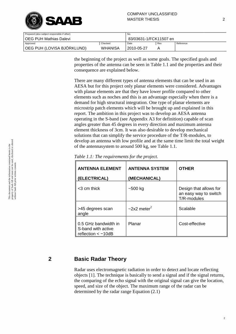
the beginning of the project as well as some goals. The specified goals and
properties of the antenna can be seen in Table 1.1 and the properties and their
consequence are explained below. There are many different types of antenna elements that can be used in an
AESA but for this project only planar elements were considered. Advantages
with planar elements are that they have lower profile compared to other
elements such as noches and this is an advantage especially when there is a
demand for high structural integration. One type of planar elements are
microstrip patch elements which will be brought up and explained in this
report. The ambition in this project was to develop an AESA antenna
operating in the S-band (see Appendix A3 for definition) capable of scan
angles greater than 45 degrees in every direction and maximum antenna
element thickness of 3cm. It was also desirable to develop mechanical
solutions that can simplify the service procedure of the T/R-modules, to
develop an antenna with low profile and at the same time limit the total weight
of the antennasystem to around 500 kg, see Table 1.1.
Table 1.1: The requirements for the project.
2 Basic Radar Theory
Radar uses electromagnetic radiation in order to detect and locate reflecting
objects [1]. The technique is basically to send a signal and if the signal returns,
the comparing of the echo signal with the original signal can give the location,
speed, and size of the object. The maximum range of the radar can be
determined by the radar range Equation (2.1)
ANTENNA ELEMENT
(ELECTRICAL)
ANTENNA SYSTEM
(MECHANICAL)
OTHER
<3 cm thick ~500 kg Design that allows for an easy way to switch T/R-modules
>45 degrees scan angle
~2x2 meter2 Scalable
0.5 GHz bandwidth in S-band with active reflection < −10dB
Planar Cost-effective
COMPANY UNCLASSIFIED
MASTER THESIS
3
Prepared (also subject responsible if other) No.
OEG PUH Mathias Dalevi 83/03631-1/FCK11507 en Approved Checked Date Rev Reference
OEG PUH (LOVISA BJÖRKLUND) WHANISA 2010-05-27 A
3
This
docu
men
t an
d t
he
info
rmat
ion c
onta
ined
her
ein i
s th
e
pro
per
ty o
f S
aab A
B a
nd m
ust
not
be
use
d,
dis
close
d o
r al
tere
d
wit
hout
Saa
b A
B p
rior
wri
tten
conse
nt.
22
2
222
44
,1
wff
t
r
R
De
P
P. (2.1)
Where Pr is the received power of the antenna, Pt is the transmitted power
from the antenna, σ is radar cross section, eff is the efficiency of the antenna, Г
is the reflection coefficient, D(θ,ϕ) is the directivity of the antenna, λ is the
wavelength, R is the distance between the antenna and the target, ρw is the
polarisation unit vector of the scattered wave and ρ is the polarization of the
antenna.
An AESA steers the antenna beam electronically which means that it can
direct its beam much faster than the conventional mechanically steered
antenna. An AESA consists of different subsystems in which each subsystem
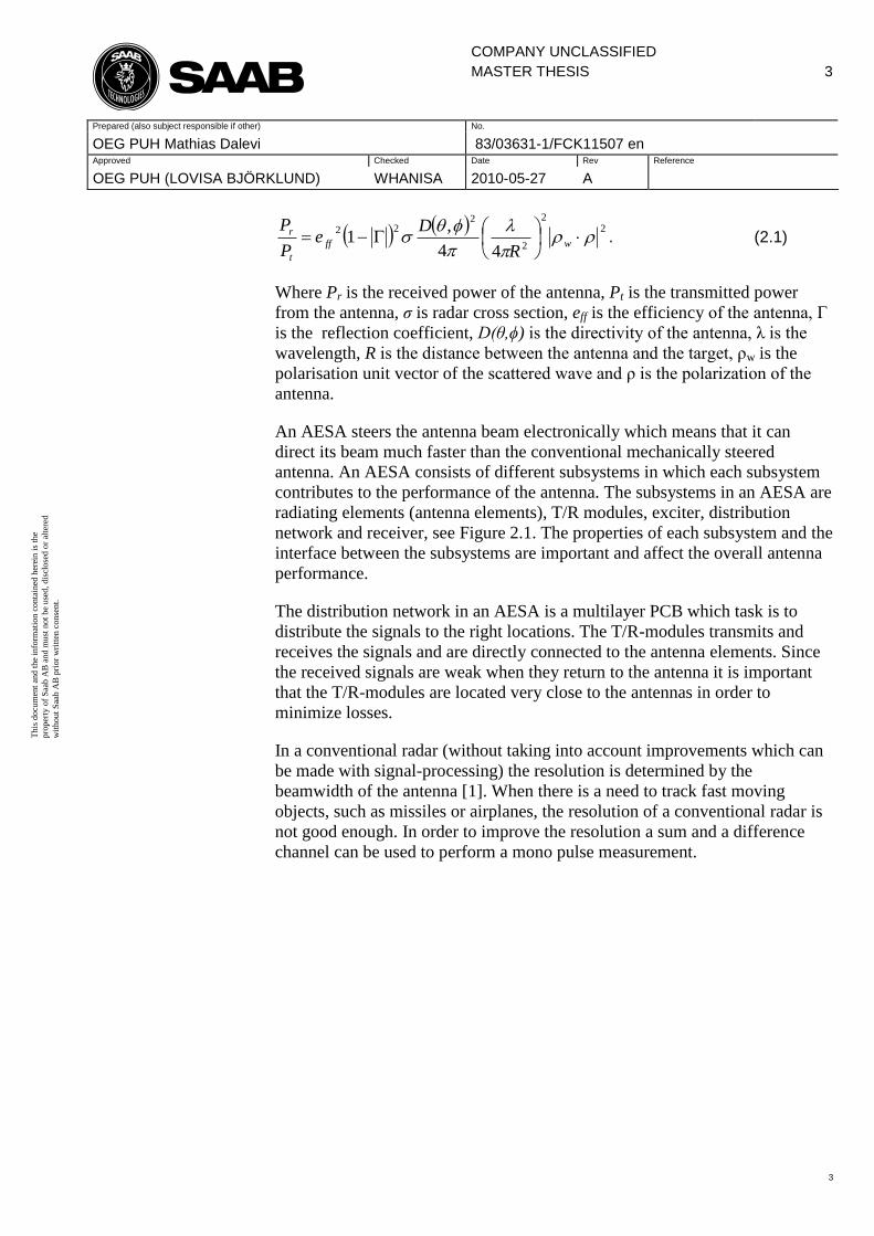
contributes to the performance of the antenna. The subsystems in an AESA are
radiating elements (antenna elements), T/R modules, exciter, distribution
network and receiver, see Figure 2.1. The properties of each subsystem and the
interface between the subsystems are important and affect the overall antenna
performance.
The distribution network in an AESA is a multilayer PCB which task is to
distribute the signals to the right locations. The T/R-modules transmits and
receives the signals and are directly connected to the antenna elements. Since
the received signals are weak when they return to the antenna it is important
that the T/R-modules are located very close to the antennas in order to
minimize losses.
In a conventional radar (without taking into account improvements which can
be made with signal-processing) the resolution is determined by the
beamwidth of the antenna [1]. When there is a need to track fast moving
objects, such as missiles or airplanes, the resolution of a conventional radar is
not good enough. In order to improve the resolution a sum and a difference
channel can be used to perform a mono pulse measurement.
COMPANY UNCLASSIFIED
MASTER THESIS
4
Prepared (also subject responsible if other) No.
OEG PUH Mathias Dalevi 83/03631-1/FCK11507 en Approved Checked Date Rev Reference
OEG PUH (LOVISA BJÖRKLUND) WHANISA 2010-05-27 A
4
This
docu
men
t an
d t
he
info
rmat
ion c
onta
ined
her
ein i
s th
e
pro
per
ty o
f S
aab A
B a
nd m
ust
not
be
use
d,
dis
close
d o
r al
tere
d
wit
hout
Saa
b A
B p
rior
wri
tten
conse
nt.
Figure 2.1: A simple illustration of the subsystem of a radar.
3 Antenna theory
3.1 Antenna Array
The radiation characteristics of an array are determined by different factors. To
make the theory easier, an ideal case is assumed where every element in the
array have the same radiation characteristics.
The radiation of the array can then be controlled by a number of design
parameters: the geometrical configuration of the overall array, the relative
displacement between the elements, the excitation amplitude and phase of the
different elements and the relative pattern of the individual elements [3]. The
ability to control these parameters independently will yield good control of the
radiation pattern of the antenna. The total field for an array is given by
AFEFEtotal . (3.1)
Where EF is the element factor which is the radiation characteristic for an
individual element and AF is the array factor which depends on the relative
distance between the elements, the excitation phase and the excitation
amplitude. For a rectangular array with the elements spaced a distance dx in
the x-direction and spaced a distance dy in the y-direction (see Figure 3.1 for
geometry) the array factor is given by
COMPANY UNCLASSIFIED
MASTER THESIS
5
Prepared (also subject responsible if other) No.
OEG PUH Mathias Dalevi 83/03631-1/FCK11507 en Approved Checked Date Rev Reference
OEG PUH (LOVISA BJÖRKLUND) WHANISA 2010-05-27 A
5
This
docu
men
t an
d t
he
info
rmat
ion c
onta
ined
her
ein i
s th
e
pro
per
ty o
f S
aab A
B a
nd m
ust
not
be
use
d,
dis
close
d o
r al
tere
d
wit
hout
Saa
b A
B p
rior
wri
tten
conse
nt.
)))cos(sin()(1(
1 1
)))cos(sin()(1(
11yyxx
kdnjN
n
M
m
kdmj
mn eeIIAF
. (3.2)
Where βx and βy are the progressive phase shift between elements in the x-
direction and the y-direction, Im1 is the excitation coefficient in the x-direction
and I1n is the excitation coefficient in the y-direction.
Figure 3.1: Geometry of a planar array configuration with the elements
positioned in a rectangular lattice. Adapted from Balanis, 2005 [3].
3.2 Microstrip patch element
Microstrip patch elements have advantages such as low profile, low cost, easy
manufacturing, and low weight, see Balanis, 2005 [3] for details. However,
there are disadvantages such as a narrow bandwidth. The most simple
configuration of a microstrip patch antenna consist of a thin metallic strip
placed on top of a dielectric layer placed above a ground plane (thin metallic
layer), see Figure 3.2.
COMPANY UNCLASSIFIED
MASTER THESIS
6
Prepared (also subject responsible if other) No.
OEG PUH Mathias Dalevi 83/03631-1/FCK11507 en Approved Checked Date Rev Reference
OEG PUH (LOVISA BJÖRKLUND) WHANISA 2010-05-27 A
6
This
docu
men
t an
d t
he
info
rmat
ion c
onta
ined
her
ein i
s th
e
pro
per
ty o
f S
aab A
B a
nd m
ust
not
be
use
d,
dis
close
d o
r al
tere
d
wit
hout
Saa
b A
B p
rior
wri
tten
conse
nt.
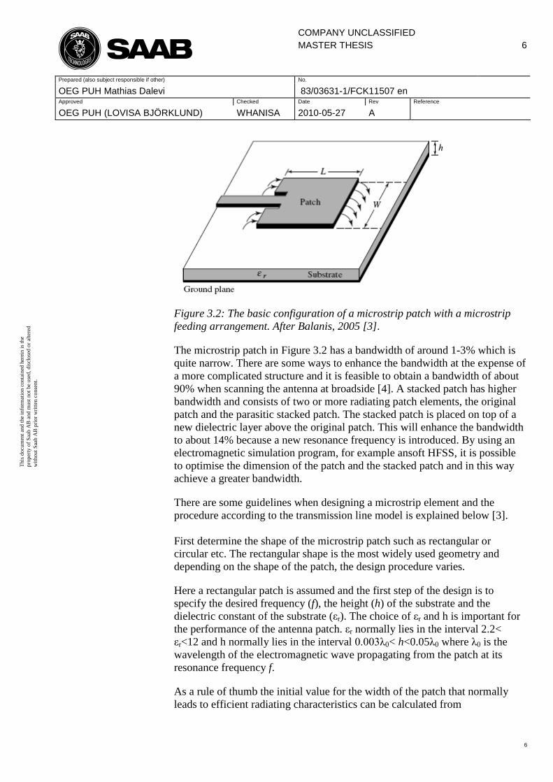
Figure 3.2: The basic configuration of a microstrip patch with a microstrip
feeding arrangement. After Balanis, 2005 [3].
The microstrip patch in Figure 3.2 has a bandwidth of around 1-3% which is
quite narrow. There are some ways to enhance the bandwidth at the expense of
a more complicated structure and it is feasible to obtain a bandwidth of about
90% when scanning the antenna at broadside [4]. A stacked patch has higher
bandwidth and consists of two or more radiating patch elements, the original
patch and the parasitic stacked patch. The stacked patch is placed on top of a
new dielectric layer above the original patch. This will enhance the bandwidth
to about 14% because a new resonance frequency is introduced. By using an
electromagnetic simulation program, for example ansoft HFSS, it is possible
to optimise the dimension of the patch and the stacked patch and in this way
achieve a greater bandwidth.
There are some guidelines when designing a microstrip element and the
procedure according to the transmission line model is explained below [3].
First determine the shape of the microstrip patch such as rectangular or
circular etc. The rectangular shape is the most widely used geometry and
depending on the shape of the patch, the design procedure varies.
Here a rectangular patch is assumed and the first step of the design is to
specify the desired frequency (f), the height (h) of the substrate and the
dielectric constant of the substrate (εr). The choice of εr and h is important for
the performance of the antenna patch. εr normally lies in the interval 2.2<
εr<12 and h normally lies in the interval 0.003λ0< h<0.05λ0 where λ0 is the
wavelength of the electromagnetic wave propagating from the patch at its
resonance frequency f.
As a rule of thumb the initial value for the width of the patch that normally
leads to efficient radiating characteristics can be calculated from
COMPANY UNCLASSIFIED
MASTER THESIS
7
Prepared (also subject responsible if other) No.
OEG PUH Mathias Dalevi 83/03631-1/FCK11507 en Approved Checked Date Rev Reference
OEG PUH (LOVISA BJÖRKLUND) WHANISA 2010-05-27 A
7
This
docu
men
t an
d t
he
info
rmat
ion c
onta
ined
her
ein i
s th
e
pro
per
ty o
f S
aab A
B a
nd m
ust
not
be
use
d,
dis
close
d o
r al
tere
d
wit
hout
Saa
b A
B p
rior
wri
tten
conse
nt.
21
0
1
2
2
rrf
CW
. (3.3)
Because of the finite dimension of the patch, the electromagnetic fields along
the edges undergo fringing which basically means that the antenna looks
longer from an electromagnetic point of view. This affects the resonance
frequency of the patch. The extent of the fringing depends on the ratio W/h
together with the dielectric constant of the substrate εr, where W is the width of
the patch and h is the height of the substrate.
Since W/h is large for microstrip patches, the fringing depends mainly of the
dielectric constant εr. When W/h>1 the effective electric constant is
2
1
, 1212
)1(
2
)1(
W
hrreffr
. (3.4)
When the effective dielectric constant is known it is possible to calculate the
effective length of the patch according to
8.0)258.0
264.03.0
412.0
,
,
h
W
h
W
h
L
effr
effr
(3.5)
LLLeff 2. (3.6)
It should be noted that the transmission line model is not very accurate and by
calculating the dimension of the patch according to this model, the resonance
frequency will probably deviate from the desired one. This model is therefore
best used in order to calculate initial values which are later optimised in an
electromagnetic simulation program.
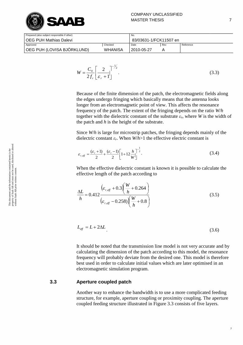
3.3 Aperture coupled patch
Another way to enhance the bandwidth is to use a more complicated feeding
structure, for example, aperture coupling or proximity coupling. The aperture
coupled feeding structure illustrated in Figure 3.3 consists of five layers.

COMPANY UNCLASSIFIED
MASTER THESIS
8
Prepared (also subject responsible if other) No.
OEG PUH Mathias Dalevi 83/03631-1/FCK11507 en Approved Checked Date Rev Reference
OEG PUH (LOVISA BJÖRKLUND) WHANISA 2010-05-27 A
8
This
docu
men
t an
d t
he
info
rmat
ion c
onta
ined
her
ein i
s th
e
pro
per
ty o
f S
aab A
B a
nd m
ust
not
be
use
d,
dis
close
d o
r al
tere
d
wit
hout
Saa
b A
B p
rior
wri
tten
conse
nt.
The 1st layer is a ground plane, the 2
nd layer is a dielectric, the 3
rd layer is
prepreg dielectric (thin dielectric that is used to bond the 2nd
and 4th
layers
together), the 4th
layer is another dielectric and the 5th
layer is another ground
plane. The 2nd
layer has a microstrip line on top of it which is used as a
feeding point for the structure.
The 5th layer is a ground plane with a slot which is excited by the microstrip
line in the 2nd
layer. This feeding structure could then be used to feed a patch
which would be placed on top of a third dielectric layer placed above the
ground plane with the slot. This configuration introduces a quite complex
feeding structure but the gain will be a bandwidth of around 14% for a single
patch
Figure 3.3: Aperture coupled configuration.
To further enhance the bandwidth it is possible to use an aperture coupled
stacked patch configuration. By using this configuration it is possible to obtain
a bandwidth of around 90%. The common denominator, between all
bandwidth-enhancement techniques is a more complex, less compact structure.
3.4 Surface-wave coupling
A problem with patch antennas is that they excite surface-waves, which are
guided by the substrate and the ground plane. In array applications, the
surface-wave coupling between antenna elements could severely degrade the
performance of the antenna. According to Nikolic, 2005 [5], this coupling
becomes important when the normalized electrical thickness h/λ0 of the
substrate has a value that fulfill the relation

COMPANY UNCLASSIFIED
MASTER THESIS
9
Prepared (also subject responsible if other) No.
OEG PUH Mathias Dalevi 83/03631-1/FCK11507 en Approved Checked Date Rev Reference
OEG PUH (LOVISA BJÖRKLUND) WHANISA 2010-05-27 A
9
This
docu
men
t an
d t
he
info
rmat
ion c
onta
ined
her
ein i
s th
e
pro
per
ty o
f S
aab A
B a
nd m
ust
not
be
use
d,
dis
close
d o
r al
tere
d
wit
hout
Saa
b A
B p
rior
wri
tten
conse
nt.
r
h
2
3.0
0
. (3.7)
When Equation.(3.7) is satisfied it is important to suppress these surface-
waves in order to improve the performance of the antenna. This can be done
by enclosing each antenna in a cavity which in the simplest way is done by
surrounding each antenna with metalized via-holes that are in contact with a
ground plane.
3.5 Grating lobes
A grating lobe is defined as a maxima other than the principal maxima of
radiation that occurs when the spacing between elements are large enough
(larger than λ/2) to permit in-phase addition of radiated fields in more than one
direction [3]. Assume a one dimensional array with N isotropic radiating
elements, uniform excitation and a spacing of distance dy (see Figure 3.1). The
the criterion for no grating lobes is then given by
)sin(1
1
0
yd. (3.8)
Where θ0 is the scan angle and λ is the wavelength of the highest frequency of
the operating band.
3.6 Wide angle impedance match
When scanning an array in different directions the reflection coefficient
changes.
This phenomenon results in degradation of the performance of the antenna
array. One approach to solve this problem is to use a Wide Angle Impedance
Match (WAIM) layer spaced in front of the array [6]. A WAIM layer consist
of one or several dielectric layers that match the reflection coefficient to wider
scan angles which improves the scanning capabilities of the antenna. A WAIM
layer could be the radome of the antenna.

COMPANY UNCLASSIFIED
MASTER THESIS
10
Prepared (also subject responsible if other) No.
OEG PUH Mathias Dalevi 83/03631-1/FCK11507 en Approved Checked Date Rev Reference
OEG PUH (LOVISA BJÖRKLUND) WHANISA 2010-05-27 A
10
This
docu
men
t an
d t
he
info
rmat
ion c
onta
ined
her
ein i
s th
e
pro
per
ty o
f S
aab A
B a
nd m
ust
not
be
use
d,
dis
close
d o
r al
tere
d
wit
hout
Saa
b A
B p
rior
wri
tten
conse
nt.
4 Concept and design
4.1 Overall antenna geometry
When designing an AESA there are basically two different architectures that
can be chosen, the tile-architecture or the brick-architecture. The different
architectures describe the orientation of the T/R-modules relative the antenna
elements. When using the tile-architecture, the T/R-modules are parallel to the
antenna elements and when using the brick-architecture the T/R-modules are
positioned perpendicular to the antenna elements. In this project several
concepts involving both brick and tile architectures have been considered but
the concept that was most promising uses tile-architecture
The most promising tile-concept has T/R-modules connected to the antenna
elements through double-sided T/R-modules (see Figure 4.1) which makes this
concept very thin and the main reason why this concept was chosen.
Figure 4.1: Illustration of how the T/R-modules would be connected to the
distribution network when normal SMP-connectors are used.
Normally a radar-system is designed so that behind the antenna elements there
are T/R-modules and behind the T/R-modules there is a distribution network.
This design makes it difficult to reach the T/R-modules in order to perform
maintenance work. Therefore, the decision was made to place the distribution
network in front of the T/R-modules which makes the service procedure of the
T/R-modules easier. It also makes is possible to combine the antenna elements
and the distribution network into one solid piece which will contribute to the
stability of the antenna and simplify the manufacture. Another advantage is
that the contact connecting the T/R-modules with the antenna elements could
be removed (see Section 4.4).
Antenna element
Distribution network
SMP connector cccocontact
TRM
COMPANY UNCLASSIFIED
MASTER THESIS
11
Prepared (also subject responsible if other) No.
OEG PUH Mathias Dalevi 83/03631-1/FCK11507 en Approved Checked Date Rev Reference
OEG PUH (LOVISA BJÖRKLUND) WHANISA 2010-05-27 A
11
This
docu
men
t an
d t
he
info
rmat
ion c
onta
ined
her
ein i
s th
e
pro
per
ty o
f S
aab A
B a
nd m
ust
not
be
use
d,
dis
close
d o
r al
tere
d
wit
hout
Saa
b A
B p
rior
wri
tten
conse
nt.
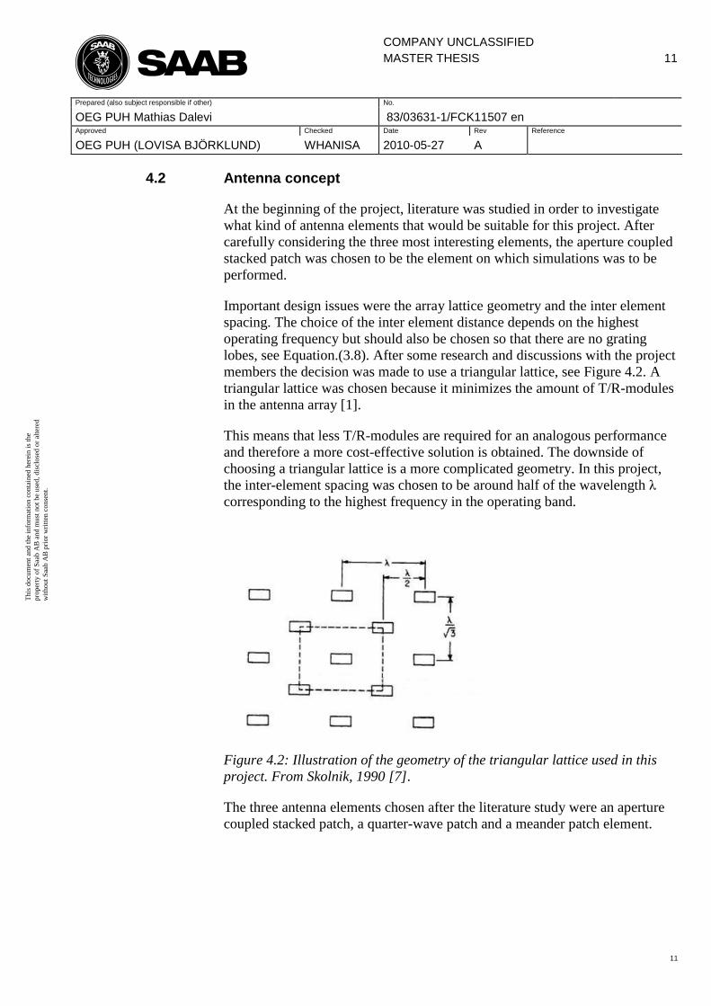
4.2 Antenna concept
At the beginning of the project, literature was studied in order to investigate
what kind of antenna elements that would be suitable for this project. After
carefully considering the three most interesting elements, the aperture coupled
stacked patch was chosen to be the element on which simulations was to be
performed.
Important design issues were the array lattice geometry and the inter element
spacing. The choice of the inter element distance depends on the highest
operating frequency but should also be chosen so that there are no grating
lobes, see Equation.(3.8). After some research and discussions with the project
members the decision was made to use a triangular lattice, see Figure 4.2. A
triangular lattice was chosen because it minimizes the amount of T/R-modules
in the antenna array [1].
This means that less T/R-modules are required for an analogous performance
and therefore a more cost-effective solution is obtained. The downside of
choosing a triangular lattice is a more complicated geometry. In this project,
the inter-element spacing was chosen to be around half of the wavelength λ
corresponding to the highest frequency in the operating band.
Figure 4.2: Illustration of the geometry of the triangular lattice used in this
project. From Skolnik, 1990 [7].
The three antenna elements chosen after the literature study were an aperture
coupled stacked patch, a quarter-wave patch and a meander patch element.
COMPANY UNCLASSIFIED
MASTER THESIS
12
Prepared (also subject responsible if other) No.
OEG PUH Mathias Dalevi 83/03631-1/FCK11507 en Approved Checked Date Rev Reference
OEG PUH (LOVISA BJÖRKLUND) WHANISA 2010-05-27 A
12
This
docu
men
t an
d t
he
info
rmat
ion c
onta
ined
her
ein i
s th
e
pro
per
ty o
f S
aab A
B a
nd m
ust
not
be
use
d,
dis
close
d o
r al
tere
d
wit
hout
Saa
b A
B p
rior
wri
tten
conse
nt.
A quarter-wave patch is smaller than a λ/2 patch. Smaller elements means that
the mutual coupling between the elements could be reduced which enables a
wider scan angle capability in one of the planes. Another good property is the
wide beamwidth. The reason not to choose this element was that because of
the connection of the element to the ground plane there will be an anti-
symmetrical current distribution which will contribute to higher cross-
polarization of the field. For some applications it may be desirable to have
very low cross-polarization. Another reason not to choose the quarter-wave
patch was that there has been few published report on this element in array
applications.
The meander element was interesting mainly because of a published report
from a group in India that illustrated properties necessary in this project, i.e. S-
band, wide scan angle up to 60 degrees and low profile [9]. After careful
consideration, the decision was made to leave this element due to doubts
concerning the feasibility of obtaining these properties with the given element.
The aperture coupled stacked patch was developed by FOI [8] and good result
had been obtained, both in simulations and in practice. Another group from
Italy [4] had also obtained good result from simulation with a similar element.
These two observations were the major reasons of choosing this type of
element.
4.3 Aperture coupled stacked patch design
The aperture coupled stacked patch was the chosen element after the literature
study and the design of the antenna element has been carried out in the
commercial software Ansoft HFSS v11.2. The element has been simulated
with periodic boundary conditions (infinite array) and has been optimised with
a non linear programming method. The design procedure for this element is
explained below.
The first step in the design procedure for this antenna element was to begin
with an element that already was designed before that had properties that were
required for this project. In this case the antenna that FOI had developed [8]
was used as a starting point when recreating and simulating the model in
HFSS, see Figure 4.3 and Figure 4.4. This element has been designed for both
vertical and horizontal polarization but in this project only one polarization has
been used.

COMPANY UNCLASSIFIED
MASTER THESIS
13
Prepared (also subject responsible if other) No.
OEG PUH Mathias Dalevi 83/03631-1/FCK11507 en Approved Checked Date Rev Reference
OEG PUH (LOVISA BJÖRKLUND) WHANISA 2010-05-27 A
13
This
docu
men
t an
d t
he
info
rmat
ion c
onta
ined
her
ein i
s th
e
pro
per
ty o
f S
aab A
B a
nd m
ust
not
be
use
d,
dis
close
d o
r al
tere
d
wit
hout
Saa
b A
B p
rior
wri
tten
conse
nt.
Figure 4.3: Original antenna element that was used as starting point in the
design [8]. The black bolded lines represents layers of copper (patch and
ground plane), the red bolded lines represents microstrip lines (fork).
Figure 4.4: Illustration of the feeding arrangement from the element which
originates from [8].The structure is constructed to radiate two polarizations,
vertical and horizontal. It consists of two perpendicular microstrip-forks and
two perpendicular H-slots.
Rogers 4350 (r = 3.48)
Rogers 4403 (r = 3.17)
Rogers 4450B (r = 3.58)
Rogers RT/duroid (r = 2.2)
Rohacell HF 71 (r = 1.09)
0.76
0.25
1.14
1.2
0.51
[mm]

COMPANY UNCLASSIFIED
MASTER THESIS
14
Prepared (also subject responsible if other) No.
OEG PUH Mathias Dalevi 83/03631-1/FCK11507 en Approved Checked Date Rev Reference
OEG PUH (LOVISA BJÖRKLUND) WHANISA 2010-05-27 A
14
This
docu
men
t an
d t
he
info
rmat
ion c
onta
ined
her
ein i
s th
e
pro
per
ty o
f S
aab A
B a
nd m
ust
not
be
use
d,
dis
close
d o
r al
tere
d
wit
hout
Saa
b A
B p
rior
wri
tten
conse
nt.
The element was first recreated for the frequencies that the element originally
had been designed for (X-band and Ku-band). The second step was to rescale
the element to work in the S-band and this was done by multiplying all the
dimensions of the element with a scaling factor Sf which was calculated with
Equation.(4.1)
)_(
)_(
elementdesiredf
elementoriginalfS f . (4.1)
Where f(original_element) is the highest frequency of the operating band for
the original antenna element and f(desired_element) is the highest frequency
of the operating band for the desired antenna element.
It was found that there was a complex dependence between the feeding
arrangement and the lower patch. This means that the element behaved
differently after the scaling-adjustment of the patch dimensions and
optimization of the element was required in order to make it function in a
similar way as before. The element was then placed into a triangular lattice.
This was followed by optimizing the different dimensions of the element: the
dimension of the feeding fork, the thickness of the dielectric layers, the
placement of the via-holes, the dimension of the H-slot and the dimensions of
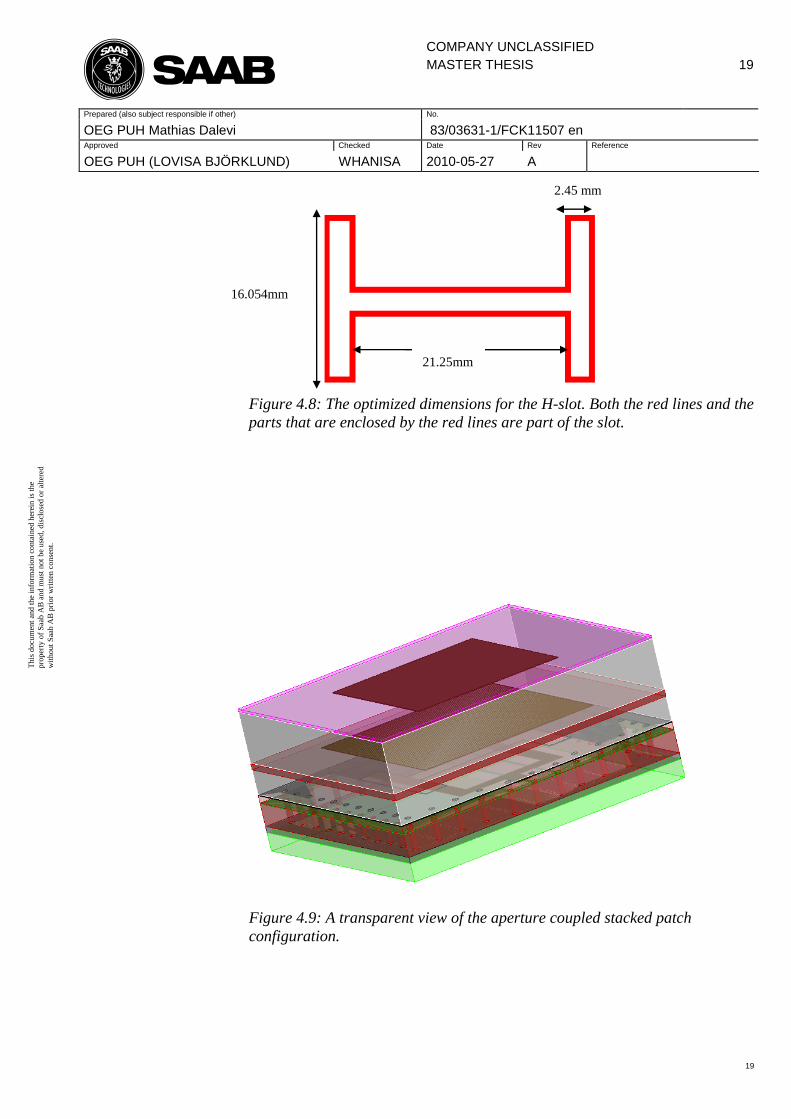
the patches (see Figure 4.9 and Figure 4.10 for illustration of the element).
A parameter that greatly influences the performance of the element is the
width of the two parallel striplines, which build up the fork. This parameter
influences the impedance of the fork and since it is directly connected to the
feeding structure it is important that they are matched, i.e. they have the same
impedance. Another example are the heights of the first two dielectric layers,
which build up the feeding structure (see Figure 3.3). This influence can be
explained by the importance of the positioning of the fork relative to the
ground plane with the H-slot and the patches, this is important for the coupling
of the different parts of the element. Other important parameters are the
dimensions of the lower and upper patches and their positioning relative one
another. It was important that these parameters were optimized since these
dimensions greatly would influence the performance of the antenna. The next
step in the design was to take the mechanical aspects under more careful
consideration since this project has intended to produce a low-weight solution.
To reduce the weight of the antenna element, the thickness of the dielectric
layers were reduced and replaced by a low-weight distance material called
Rohacell, which from an electromagnetic point of view behaves as air. Since
Rohacell is electrically shorter than the dielectric material it replaced, the new
Rohacell layers had to be thicker.

COMPANY UNCLASSIFIED
MASTER THESIS
15
Prepared (also subject responsible if other) No.
OEG PUH Mathias Dalevi 83/03631-1/FCK11507 en Approved Checked Date Rev Reference
OEG PUH (LOVISA BJÖRKLUND) WHANISA 2010-05-27 A
15
This
docu
men
t an
d t
he
info
rmat
ion c
onta
ined
her
ein i
s th
e
pro
per
ty o
f S
aab A
B a
nd m
ust
not
be
use
d,
dis
close
d o
r al
tere
d
wit
hout
Saa
b A
B p
rior
wri
tten
conse
nt.
The feeding arrangement had to be re-optimized with the rohacell layer
because it turned out that there was a dependence of the positioning of the
feeding arrangement as well. After the procedure of reducing the weight of the
element it was time to replace some of the dielectric layers that was used in the
element.
RT/duroid 5880 which was used initially is a Teflon based material and it is
difficult to attach it to other materials with glue. This means that if this
material would have been used the antenna would have been difficult to
assemble. The materials Rogers 4350B and FR-4 were chosen instead because
they function well in the operating frequency range used in this project, they
are easy to assemble and they are used widely in industry which makes it fast
and easy to order and receive the materials. The next step was to introduce a
more practical arrangement to feed the microstrip fork. Until this point, the
feed had been a coaxial probe which is impractical to manufacture.
4.4 Antenna feed
The antenna feed consist of a metalized via hole, called a signal-via, which
connect the microstrip fork with a SMP connector. The signal-via goes
through the Rogers 4350B layers to a etched pattern at the lower ground plane,
see Figure 4.5. This pattern is connected to the SMP-connector which enables
the signal to go from the SMP-conncector to the microstrip fork.
Figure 4.5: The figure shows the etched pattern in the ground plane which is
used in the prototype (the vertical lines doesn’t represent an etched pattern
and should be interpreted as part of the ground plane. The signal-via is
indicated by the grey dot. The distance between the pad and the ground plane
is 0.250 mm in the prototype but has been adjusted to around 0.110 mm for the
optimized element.
In order to prevent parallel plate modes from propagating it was necessary to
enclose each antenna element in a cavity. This was done by surrounding each
antenna element with metallised via-holes which connect the lower ground
plane and the ground plane with the H-slot. In the simulations, the vias that
build up the cavity were simulated as perfect conducting sheets in order to
reduce the complexity of the system.
COMPANY UNCLASSIFIED
MASTER THESIS
16
Prepared (also subject responsible if other) No.
OEG PUH Mathias Dalevi 83/03631-1/FCK11507 en Approved Checked Date Rev Reference
OEG PUH (LOVISA BJÖRKLUND) WHANISA 2010-05-27 A
16
This
docu
men
t an
d t
he
info
rmat
ion c
onta
ined
her
ein i
s th
e
pro
per
ty o
f S
aab A
B a
nd m
ust
not
be
use
d,
dis
close
d o
r al
tere
d
wit
hout
Saa
b A
B p
rior
wri
tten
conse
nt.
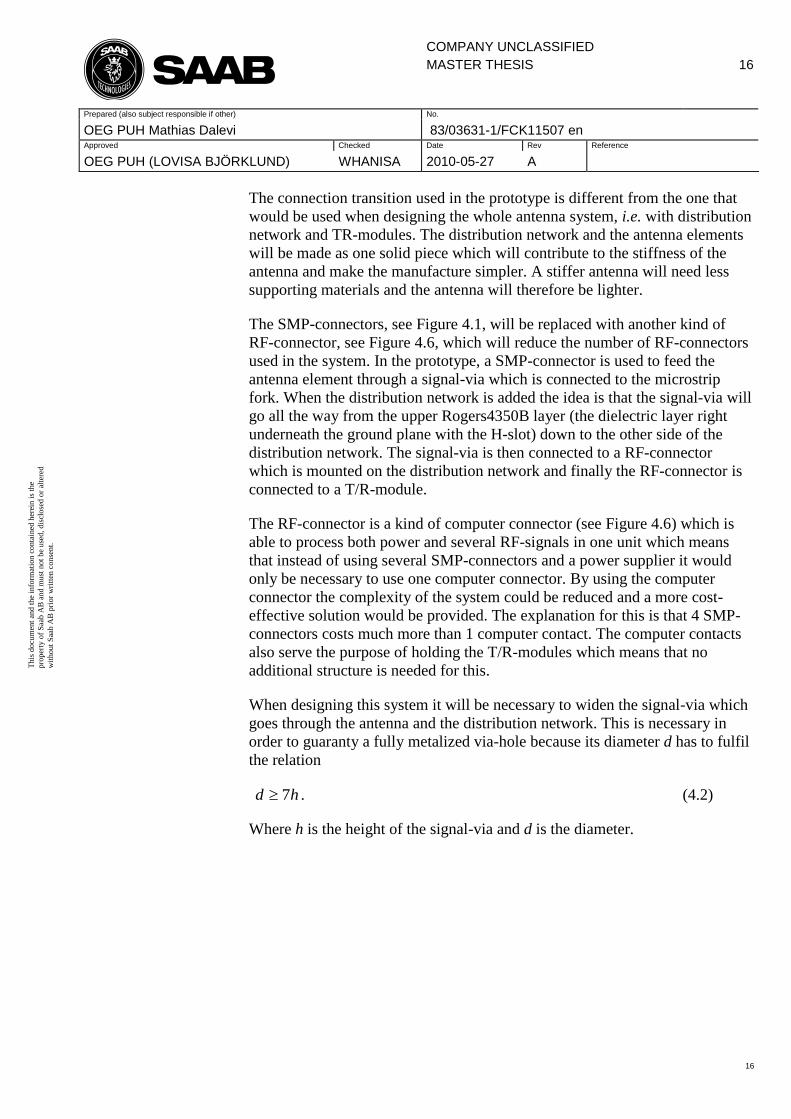
The connection transition used in the prototype is different from the one that
would be used when designing the whole antenna system, i.e. with distribution
network and TR-modules. The distribution network and the antenna elements
will be made as one solid piece which will contribute to the stiffness of the
antenna and make the manufacture simpler. A stiffer antenna will need less
supporting materials and the antenna will therefore be lighter.
The SMP-connectors, see Figure 4.1, will be replaced with another kind of
RF-connector, see Figure 4.6, which will reduce the number of RF-connectors
used in the system. In the prototype, a SMP-connector is used to feed the
antenna element through a signal-via which is connected to the microstrip
fork. When the distribution network is added the idea is that the signal-via will
go all the way from the upper Rogers4350B layer (the dielectric layer right
underneath the ground plane with the H-slot) down to the other side of the
distribution network. The signal-via is then connected to a RF-connector
which is mounted on the distribution network and finally the RF-connector is
connected to a T/R-module.
The RF-connector is a kind of computer connector (see Figure 4.6) which is
able to process both power and several RF-signals in one unit which means
that instead of using several SMP-connectors and a power supplier it would
only be necessary to use one computer connector. By using the computer
connector the complexity of the system could be reduced and a more cost-
effective solution would be provided. The explanation for this is that 4 SMP-
connectors costs much more than 1 computer contact. The computer contacts
also serve the purpose of holding the T/R-modules which means that no
additional structure is needed for this.
When designing this system it will be necessary to widen the signal-via which
goes through the antenna and the distribution network. This is necessary in
order to guaranty a fully metalized via-hole because its diameter d has to fulfil
the relation
hd 7 . (4.2)
Where h is the height of the signal-via and d is the diameter.

COMPANY UNCLASSIFIED
MASTER THESIS
17
Prepared (also subject responsible if other) No.
OEG PUH Mathias Dalevi 83/03631-1/FCK11507 en Approved Checked Date Rev Reference
OEG PUH (LOVISA BJÖRKLUND) WHANISA 2010-05-27 A
17
This
docu
men
t an
d t
he
info
rmat
ion c
onta
ined
her
ein i
s th
e
pro
per
ty o
f S
aab A
B a
nd m
ust
not
be
use
d,
dis
close
d o
r al
tere
d
wit
hout
Saa
b A
B p
rior
wri
tten
conse
nt.
Figure 4.6: Illustration of the computer-contact which is used instead of the 4
SMP-connectors in Figure 4.1.
4.5 Aperture coupled stacked patch final version
The final version of the aperture coupled stacked patch consists of several
layers as shown in Figure 4.10 where the first layer is a Rogers 4350B
dielectric layer placed above a ground plane with a microstrip fork etched on
top of it, (see Figure 4.7 for optimized dimensions of the fork).
The next layer is another Rogers 4350B layer which has a ground plane with
an H-slot on top of it, see Figure 4.8 for optimized dimensions of the H-slot.
From the ground plane with the H-slot to the other ground plane, near the
edges there are metallised via holes that connect the two ground planes to each
other. In this way the lower structure (red in Figure 4.9) becomes a cavity that
isolates the individual elements from unwanted radiation from neighbouring
elements. This cavity also prevents that unwanted parallel modes will occur.
The next layer is a layer of rohacell which is followed by a Rogers 4350B
dielectric layer with a microstrip patch on top of it. The structure then
continues with a layer of rohacell and above the rohacell there is a layer of FR-
4 with a stacked patch at its bottom side, see Figure 4.9 and Figure 4.10 for
geometry.
In addition of holding the stacked patch, the FR-4 could work as a radome, i.e.
a protecting layer against weather conditions. However in most cases it will be
necessary to place a conventional radome on top of the element because the
antenna will not be stiff enough in order to allow for building the complete
2×2 meter2 system. A conventional radome means that there is a quarter
wavelength of rohacell with a protective layer on top of it such as FR-4.
COMPANY UNCLASSIFIED
MASTER THESIS
18
Prepared (also subject responsible if other) No.
OEG PUH Mathias Dalevi 83/03631-1/FCK11507 en Approved Checked Date Rev Reference
OEG PUH (LOVISA BJÖRKLUND) WHANISA 2010-05-27 A
18
This
docu
men
t an
d t
he
info
rmat
ion c
onta
ined
her
ein i
s th
e
pro
per
ty o
f S
aab A
B a
nd m
ust
not
be
use
d,
dis
close
d o
r al
tere
d
wit
hout
Saa
b A
B p
rior
wri
tten
conse
nt.
The quarter-wavelength of the distance-material is required so that the
radiation not will be exposed of humidity and other weather related conditions
because it could affect the radiation characteristics of the antenna. The radome
for this antenna will apart from making the antenna more solid and protecting
it from weather conditions, also serve as a WAIM-layer, see Section 3.6. This
means that the radome will help the antenna to be matched for high scan
angles and boost its performance. Note that the dielectric constant of the
rohacell in the radome has another value than the other rohacell, see Figure
4.10. The ultimate 2 mm layer of FR-4 can with advantages be switched to
another material called cyanate ester which has both better mechanical and
electrical properties than FR-4.
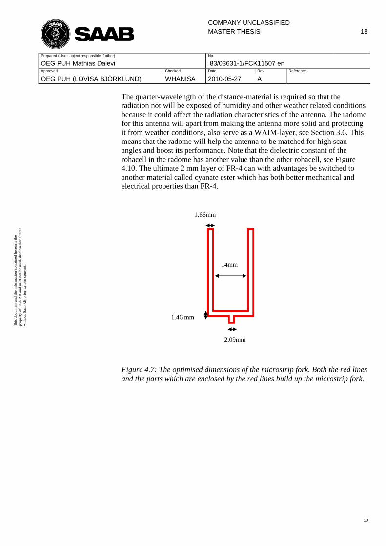
Figure 4.7: The optimised dimensions of the microstrip fork. Both the red lines
and the parts which are enclosed by the red lines build up the microstrip fork.
14mm
1.46 mm
mm
1.66mm
2.09mm
COMPANY UNCLASSIFIED
MASTER THESIS
19
Prepared (also subject responsible if other) No.
OEG PUH Mathias Dalevi 83/03631-1/FCK11507 en Approved Checked Date Rev Reference
OEG PUH (LOVISA BJÖRKLUND) WHANISA 2010-05-27 A
19
This
docu
men
t an
d t
he
info
rmat
ion c
onta
ined
her
ein i
s th
e
pro
per
ty o
f S
aab A
B a
nd m
ust
not
be
use
d,
dis
close
d o
r al
tere
d
wit
hout
Saa
b A
B p
rior
wri
tten
conse
nt.
Figure 4.8: The optimized dimensions for the H-slot. Both the red lines and the
parts that are enclosed by the red lines are part of the slot.
Figure 4.9: A transparent view of the aperture coupled stacked patch
configuration.
16.054mm
2.45 mm
21.25mm
COMPANY UNCLASSIFIED
MASTER THESIS
20
Prepared (also subject responsible if other) No.
OEG PUH Mathias Dalevi 83/03631-1/FCK11507 en Approved Checked Date Rev Reference
OEG PUH (LOVISA BJÖRKLUND) WHANISA 2010-05-27 A
20
This
docu
men
t an
d t
he
info
rmat
ion c
onta
ined
her
ein i
s th
e
pro
per
ty o
f S
aab A
B a
nd m
ust
not
be
use
d,
dis
close
d o
r al
tere
d
wit
hout
Saa
b A
B p
rior
wri
tten
conse
nt.
Figure 4.10: Illustration of the layers of the Aperture coupled stacked patch
configuration and the distribution network (light-green bottom plate).
Apparaturkopplad
stackad patch
Thickness (without
distribution network and
radome) =17.589 mm
Ground-plane of copper
(black)
Thickness=0,052 mm
Rogers 4350B: (red)
Thickness=2,388 mm
Rogers4450B: (green)
Thickness=0,102 mm
Rogers 4350B: (red)
Thickness=0.946 mm
Ground-plane of copper
(black)
Thickness=0,035 mm
Rohacell: ( εr=1.09,
white)
Thickness=4,7 mm
Patch of copper
Thickness=0.017 mm
Rogers4350B: (red)
Thickness=0,762 mm
Rohacell: ( εr=1.09,
white)
Thickness=8,17 mm
FR-4: (purple)
Thickness=0,4 mm
Patch of copper
Thickness=0.017 mm
Distribution-network
12 lager Rogers 4350B
Thickness=3mm, (light-
green)
Radome:
FR-4(or cyanate ester):
Thickness= 2mm.
Radome:
FR-4: (purple)
(or cyanate ester)
Thickness= 2mm
Rohacell (εr=1.5, white):
Thickness =20 mm

COMPANY UNCLASSIFIED
MASTER THESIS
21
Prepared (also subject responsible if other) No.
OEG PUH Mathias Dalevi 83/03631-1/FCK11507 en Approved Checked Date Rev Reference
OEG PUH (LOVISA BJÖRKLUND) WHANISA 2010-05-27 A
21
This
docu
men
t an
d t
he
info
rmat
ion c
onta
ined
her
ein i
s th
e
pro
per
ty o
f S
aab A
B a
nd m
ust
not
be
use
d,
dis
close
d o
r al
tere
d
wit
hout
Saa
b A
B p
rior
wri
tten
conse
nt.
4.6 Quarter wave patches
A quarter-wave patch, also called a planar inverted-F antenna (PIFA-antenna)
is illustrated in Figure 4.11. The quarter-wave patch is put together in the same
way as a regular patch with the difference that a shortening pin is used to
terminate the patch to the ground plane at a point where the electrical field of
the resonant mode is zero [10]. By shortening the patch it is possible to reduce
the length of the patch to a quarter-wavelength. Holub and Milan, 2008 [11]
has shows that with menaderly folded shorted-patches it is possible to reduce
the length of the patch with up to λ/16. However, these configurations are too
complex and not practical for array applications because these elements have a
narrower bandwidth and the degree of freedom when designing these elements
are reduced. Conclusively, it would not be possible, for example, to put
together an aperture coupled stacked λ/16 patch. It should be possible to put
together an aperture coupled stacked quarter wave patch without complicating
the element too much and this could be done by shortening the patch with a
metalized via that connect the ground-plane with the H-slot to the patch. This
configuration is more complicated than the regular configuration which has
been investigated during this project and one interesting thing to investigate is
how much the metalized via would change, if at all, the performance of the
antenna. Another downside of using a quarter-wave patch is that the material
between the ground-plane and the patch has to be a dielectric material
compatible to PCB-technology.
This means that it is not possible to use the low-weight distance material
rohacell which has been used in this project. This will increase the weight of
the antenna and if this parameter of the antenna needs to be minimized this is
probably not a good solution. Another good property which has been
published by Chair el al, 1999 [12] was big bandwidth improvement
compared to the half-wave patch and another bad property was the high cross-
polarisation of the field, especially in the H-plane [12].
Figure 4.11: A simple quarter-wave patch configuration. From Waterhouse,
1995 [10].

COMPANY UNCLASSIFIED
MASTER THESIS
22
Prepared (also subject responsible if other) No.
OEG PUH Mathias Dalevi 83/03631-1/FCK11507 en Approved Checked Date Rev Reference
OEG PUH (LOVISA BJÖRKLUND) WHANISA 2010-05-27 A
22
This
docu
men
t an
d t
he
info
rmat
ion c
onta
ined
her
ein i
s th
e
pro
per
ty o
f S
aab A
B a
nd m
ust
not
be
use
d,
dis
close
d o
r al
tere
d
wit
hout
Saa
b A
B p
rior
wri
tten
conse
nt.
4.7 Meander patch
As mentioned earlier, a meander-patch was considered in the literature-study,
see Figure 4.12. The specific element considered by Beenamole et al., 2007
[9] doesn’t have the qualities required for this project but the possibility to use
this element in a more complicated configuration with broader bandwidth
could be very interesting. An example of a configuration which would be
suitable is the aperture coupled stacked meander patch configuration which
there haven’t, to the author’s knowledge, been any published reports of. The
aperture coupled stacked meander-patch is like the regular aperture coupled
stacked patch configuration with the difference that the lower or upper patch is
switched to a meander-patch instead of the regular patch. However, there is a
problem with the dimensions of the meander-patch considered by Beenamole
et al., 2007 [9] because it is too large to fit in the available space in the
antenna geometry.
Figure 4.12: Dimension and geometry of the meander-patch considered in the
literature-study From Beenamole et al., 2007 [9] .
5 Prototype
5.1 Antenna parts
The patch, the stacked patch and the feeding-substrate are all manufactured
with printed circuit board technology (PCB-technology), see Figure 4.10 for
illustration of the different layers of the element. To place an order of the
PCBs, a blueprint of the three boards has been made in the commercial
software Allegro, Figure 5.1 and Figure 5.2 show the blueprint of the PCB
which contain the feeding arrangement of the antenna.
COMPANY UNCLASSIFIED
MASTER THESIS
23
Prepared (also subject responsible if other) No.
OEG PUH Mathias Dalevi 83/03631-1/FCK11507 en Approved Checked Date Rev Reference
OEG PUH (LOVISA BJÖRKLUND) WHANISA 2010-05-27 A
23
This
docu
men
t an
d t
he
info
rmat
ion c
onta
ined
her
ein i
s th
e
pro
per
ty o
f S
aab A
B a
nd m
ust
not
be
use
d,
dis
close
d o
r al
tere
d
wit
hout
Saa
b A
B p
rior
wri
tten
conse
nt.
The company Teltex has been selected to manufacture the PCBs. The
materials that have been chosen for this project are Rogers 4350B and FR-4.
They function well in the operating frequency range and they are used widely
in industry which makes it fast and easy to order and receive the material from
Teltex.
The thickness of the material comes with standardised thicknesses which limit
the design freedom of the antenna. One standard thickness of the Rogers
4350B material had been mixed up with another material called Rogers 4003C
when it was delivered to Teltex and in order to speed-up the delivery of the
product it was necessary to switch this specific PCB to the new material. This
switch has caused changes to both the mechanical and electrical properties of
the antenna, however since the material has similar properties as the original
Rogers 4350B material, the changes are small enough to be acceptable. When
the PCBs were obtained from Teltex, the SMP-connectors were surface-
mounted on the feeding-substrate in the production-facility at Saab Electronic
Defense Systems. Some problems were encountered here due to the large
dimension of the PCB and due to the fact that the PCB had an error in its
design but these problems were solved.
The rohacell-sheets that were used in this project are called HF71 and the
company Hagema was selected to slice the rohacell into pieces according to
Figure 4.10. Hagema was also chosen to manufacture the aluminium sheets
which support the antenna structure, see Section 5.2. When the RF-connectors
had been mounted it was time for the rohacell, the mechanics and the PCBs to
be attached together with very strong glue at the workshop of Saab Electronic
Defense Systems. In order to glue all pieces together in an accurate way, two
reference-holes have been made at the edges of every piece of the antenna, see
Figure 5.2. By placing a pin in each hole it is possible to glue the pieces of the
antenna in a precise way.

COMPANY UNCLASSIFIED
MASTER THESIS
24
Prepared (also subject responsible if other) No.
OEG PUH Mathias Dalevi 83/03631-1/FCK11507 en Approved Checked Date Rev Reference
OEG PUH (LOVISA BJÖRKLUND) WHANISA 2010-05-27 A
24
This
docu
men
t an
d t
he
info
rmat
ion c
onta
ined
her
ein i
s th
e
pro
per
ty o
f S
aab A
B a
nd m
ust
not
be
use
d,
dis
close
d o
r al
tere
d
wit
hout
Saa
b A
B p
rior
wri
tten
conse
nt.
Figure 5.1: The PCB containing the pattern of the fork and via-holes (green).
The two boards in Figure 5.1 and Figure 5.2 were from the beginning two
separate circuit-boards but in a later stage they have been bonded together
with a prepreg material called Rogers 4450B that has similar properties as the
two boards. This will create a transition region in the material which is
anisotropic with varying thickness and dielectric constant. Since this antenna
is constructed for the S-band, the wavelength should be long enough so that
these irregularities will not have a major impact of the performance of the
antenna but nonetheless it will have a measurable effect. Another comment
regarding the antenna element in the middle of the first row and the antenna
element in the middle of the 10th
row is that these elements could be
functioning differently in comparison to the other elements. The reason for
this is that when the PCBs were manufactured, the machine required that there
were two holes in the PCBs and since the size of the antenna array was close
to the actual panel-size available, the drilled holes will be very close to these
two antenna elements and they might be affected by it.
COMPANY UNCLASSIFIED
MASTER THESIS
25
Prepared (also subject responsible if other) No.
OEG PUH Mathias Dalevi 83/03631-1/FCK11507 en Approved Checked Date Rev Reference
OEG PUH (LOVISA BJÖRKLUND) WHANISA 2010-05-27 A
25
This
docu
men
t an
d t
he
info
rmat
ion c
onta
ined
her
ein i
s th
e
pro
per
ty o
f S
aab A
B a
nd m
ust
not
be
use
d,
dis
close
d o
r al
tere
d
wit
hout
Saa
b A
B p
rior
wri
tten
conse
nt.
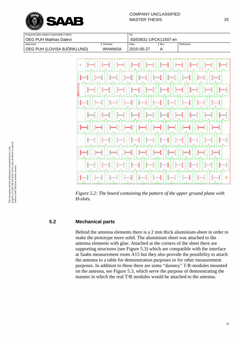
Figure 5.2: The board containing the pattern of the upper ground plane with
H-slots.
5.2 Mechanical parts
Behind the antenna elements there is a 2 mm thick aluminium-sheet in order to
make the prototype more solid. The aluminium sheet was attached to the
antenna elements with glue. Attached at the corners of the sheet there are
supporting structures (see Figure 5.3) which are compatible with the interface
at Saabs measurement room A15 but they also provide the possibility to attach
the antenna to a table for demonstration purposes or for other measurement
purposes. In addition to these there are some “dummy” T/R-modules mounted
on the antenna, see Figure 5.3, which serve the purpose of demonstrating the
manner in which the real T/R modules would be attached to the antenna.

COMPANY UNCLASSIFIED
MASTER THESIS
26
Prepared (also subject responsible if other) No.
OEG PUH Mathias Dalevi 83/03631-1/FCK11507 en Approved Checked Date Rev Reference
OEG PUH (LOVISA BJÖRKLUND) WHANISA 2010-05-27 A
26
This
docu
men
t an
d t
he
info
rmat
ion c
onta
ined
her
ein i
s th
e
pro
per
ty o
f S
aab A
B a
nd m
ust
not
be
use
d,
dis
close
d o
r al
tere
d
wit
hout
Saa
b A
B p
rior
wri
tten
conse
nt.
Figure 5.3: Illustration of the fully assembled prototype as seen from the
back/rear
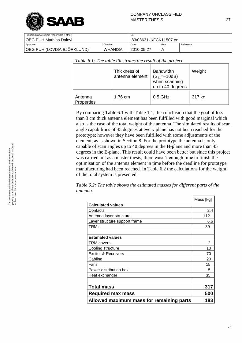
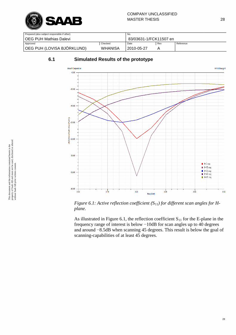
6 Result
The goals of the project were to design a low-weight, thin, S-band antenna
with 0.5 GHz bandwidth with scan angle capabilities of at least 45 degrees at
every plane with less than −10dB reflections see Table 1.1. The actual result of
the project can be seen in Table 6.1.
COMPANY UNCLASSIFIED
MASTER THESIS
27
Prepared (also subject responsible if other) No.
OEG PUH Mathias Dalevi 83/03631-1/FCK11507 en Approved Checked Date Rev Reference
OEG PUH (LOVISA BJÖRKLUND) WHANISA 2010-05-27 A
27
This
docu
men
t an
d t
he
info
rmat
ion c
onta
ined
her
ein i
s th
e
pro
per
ty o
f S
aab A
B a
nd m
ust
not
be
use
d,
dis
close
d o
r al
tere
d
wit
hout
Saa
b A
B p
rior
wri
tten
conse
nt.
Table 6.1: The table illustrates the result of the project.
Thickness of antenna element
Bandwidth (S11=−10dB) when scanning up to 40 degrees
Weight
Antenna Properties
1.76 cm 0.5 GHz 317 kg
By comparing Table 6.1 with Table 1.1, the conclusion that the goal of less
than 3 cm thick antenna element has been fulfilled with good marginal which
also is the case of the total weight of the antenna. The simulated results of scan
angle capabilities of 45 degrees at every plane has not been reached for the
prototype; however they have been fulfilled with some adjustments of the
element, as is shown in Section 8. For the prototype the antenna is only
capable of scan angles up to 40 degrees in the H-plane and more than 45
degrees in the E-plane. This result could have been better but since this project
was carried out as a master thesis, there wasn’t enough time to finish the
optimisation of the antenna element in time before the deadline for prototype
manufacturing had been reached. In Table 6.2 the calculations for the weight
of the total system is presented.
Table 6.2: The table shows the estimated masses for different parts of the
antenna.
Mass [kg]
Calculated values
Contacts 2.4
Antenna layer structure 112
Layer structure support frame 6.6
TRM:s 39
Estimated values
TRM covers 2
Cooling structure 10
Exciter & Receivers 70
Cabling 20
Fans 15
Power distribution box 5
Heat exchanger 35
Total mass 317
Required max mass 500
Allowed maximum mass for remaining parts 183
COMPANY UNCLASSIFIED
MASTER THESIS
28
Prepared (also subject responsible if other) No.
OEG PUH Mathias Dalevi 83/03631-1/FCK11507 en Approved Checked Date Rev Reference
OEG PUH (LOVISA BJÖRKLUND) WHANISA 2010-05-27 A
28
This
docu
men
t an
d t
he
info
rmat
ion c
onta
ined
her
ein i
s th
e
pro
per
ty o
f S
aab A
B a
nd m
ust
not
be
use
d,
dis
close
d o
r al
tere
d
wit
hout
Saa
b A
B p
rior
wri
tten
conse
nt.
6.1 Simulated Results of the prototype
Figure 6.1: Active reflection coefficient (S11) for different scan angles for H-
plane.
As illustrated in Figure 6.1, the reflection coefficient S11 for the E-plane in the
frequency range of interest is below −10dB for scan angles up to 40 degrees
and around −8.5dB when scanning 45 degrees. This result is below the goal of
scanning-capabilities of at least 45 degrees.

COMPANY UNCLASSIFIED
MASTER THESIS
29
Prepared (also subject responsible if other) No.
OEG PUH Mathias Dalevi 83/03631-1/FCK11507 en Approved Checked Date Rev Reference
OEG PUH (LOVISA BJÖRKLUND) WHANISA 2010-05-27 A
29
This
docu
men
t an
d t
he
info
rmat
ion c
onta
ined
her
ein i
s th
e
pro
per
ty o
f S
aab A
B a
nd m
ust
not
be
use
d,
dis
close
d o
r al
tere
d
wit
hout
Saa
b A
B p
rior
wri
tten
conse
nt.
Figure 6.2: Active reflection coefficient (S11) for different scan angles for D-
plane (diagonal plane).
The reason to show the diagonal-plane is that the antenna elements are
positioned in a triangular lattice and sometimes when this is the case,
performance is degraded in this plane. This is not the result in this case as
illustrated by Figure 6.2. As illustrated in Figure 6.2, the reflection coefficient
S11 for the D-plane is below −10dB in the frequency range of interest when
scanning the array 45 degrees and below −8dB when scanning 60 degrees.
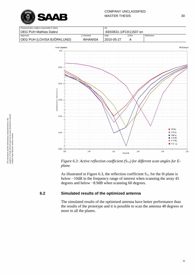
COMPANY UNCLASSIFIED
MASTER THESIS
30
Prepared (also subject responsible if other) No.
OEG PUH Mathias Dalevi 83/03631-1/FCK11507 en Approved Checked Date Rev Reference
OEG PUH (LOVISA BJÖRKLUND) WHANISA 2010-05-27 A
30
This
docu
men
t an
d t
he
info
rmat
ion c
onta
ined
her
ein i
s th
e
pro
per
ty o
f S
aab A
B a
nd m
ust
not
be
use
d,
dis
close
d o
r al
tere
d
wit
hout
Saa
b A
B p
rior
wri
tten
conse
nt.
Figure 6.3: Active reflection coefficient (S11) for different scan angles for E-
plane.
As illustrated in Figure 6.3, the reflection coefficient S11 for the H-plane is
below −10dB in the frequency range of interest when scanning the array 45
degrees and below −8.9dB when scanning 60 degrees.
6.2 Simulated results of the optimized antenna
The simulated results of the optimised antenna have better performance than
the results of the prototype and it is possible to scan the antenna 48 degrees or
more in all the planes.
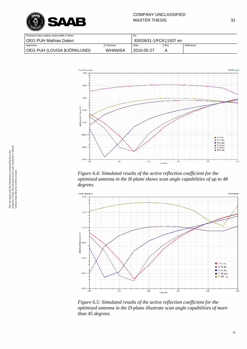
COMPANY UNCLASSIFIED
MASTER THESIS
31
Prepared (also subject responsible if other) No.
OEG PUH Mathias Dalevi 83/03631-1/FCK11507 en Approved Checked Date Rev Reference
OEG PUH (LOVISA BJÖRKLUND) WHANISA 2010-05-27 A
31
This
docu
men
t an
d t
he
info
rmat
ion c
onta
ined
her
ein i
s th
e
pro
per
ty o
f S
aab A
B a
nd m
ust
not
be
use
d,
dis
close
d o
r al
tere
d
wit
hout
Saa
b A
B p
rior
wri
tten
conse
nt.
Figure 6.4: Simulated results of the active reflection coefficient for the
optimised antenna in the H-plane shows scan angle capabilities of up to 48
degrees.
Figure 6.5: Simulated results of the active reflection coefficient for the
optimised antenna in the D-plane illustrate scan angle capabilities of more
than 45 degrees.

COMPANY UNCLASSIFIED
MASTER THESIS
32
Prepared (also subject responsible if other) No.
OEG PUH Mathias Dalevi 83/03631-1/FCK11507 en Approved Checked Date Rev Reference
OEG PUH (LOVISA BJÖRKLUND) WHANISA 2010-05-27 A
32
This
docu
men
t an
d t
he
info
rmat
ion c
onta
ined
her
ein i
s th
e
pro
per
ty o
f S
aab A
B a
nd m
ust
not
be
use
d,
dis
close
d o
r al
tere
d
wit
hout
Saa
b A
B p
rior
wri
tten
conse
nt.
Figure 6.6: Simulated results of the active reflection coefficient for the
optimised antenna in the E-plane illustrate scan angle capabilities of more
than 45 degrees.
6.3 General measurement theory
The driving impedance of an antenna element in an array has two parts, the
self impedance and the mutual impedance (which is caused by other elements
in the array or by interfering obstacles), see [3]. The sum of all contributions
of an individual antenna elements impedance is called the active reflection
coefficient, Γa. To measure Γ
a one must measure the coupling between all the
antenna elements in the array, see [13]. In order to measure the coupling
between 2 elements in an array it is necessary to terminate all the other
elements to 50 ohm and then measure the S-parameters from the two ports of
the network analyser, S11, S12, S21 and S22. To measure the active reflection
coefficient for one element one must measure and sum the coupling between
this element and all other elements of the array. So, for example, to measure Γa
for one antenna element in an array of 100 elements it is necessary to perform
99 measurements.
The results which HFSS illustrates are of the active reflection coefficient.
HFSS uses periodic boundary condition which means that an infinite number
of antenna elements are assumed in the model. So how well the measured
results coincide with the simulated results depends on the accuracy of the
simulated model and on how many elements there are in the array.
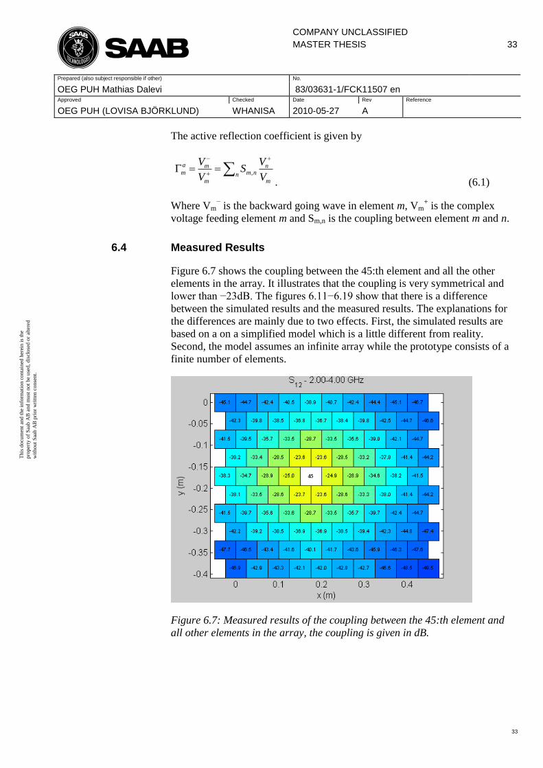
COMPANY UNCLASSIFIED
MASTER THESIS
33
Prepared (also subject responsible if other) No.
OEG PUH Mathias Dalevi 83/03631-1/FCK11507 en Approved Checked Date Rev Reference
OEG PUH (LOVISA BJÖRKLUND) WHANISA 2010-05-27 A
33
This
docu
men
t an
d t
he
info
rmat
ion c
onta
ined
her
ein i
s th
e
pro
per
ty o
f S
aab A
B a
nd m
ust
not
be
use
d,
dis
close
d o
r al
tere
d
wit
hout
Saa
b A
B p
rior
wri
tten
conse
nt.
The active reflection coefficient is given by
m
n
n nm
m
ma
mV
VS
V
V
,
. (6.1)
Where Vm− is the backward going wave in element m, Vm
+ is the complex
voltage feeding element m and Sm,n is the coupling between element m and n.
6.4 Measured Results
Figure 6.7 shows the coupling between the 45:th element and all the other
elements in the array. It illustrates that the coupling is very symmetrical and
lower than −23dB. The figures 6.11−6.19 show that there is a difference
between the simulated results and the measured results. The explanations for
the differences are mainly due to two effects. First, the simulated results are
based on a on a simplified model which is a little different from reality.
Second, the model assumes an infinite array while the prototype consists of a
finite number of elements.
Figure 6.7: Measured results of the coupling between the 45:th element and
all other elements in the array, the coupling is given in dB.

COMPANY UNCLASSIFIED
MASTER THESIS
34
Prepared (also subject responsible if other) No.
OEG PUH Mathias Dalevi 83/03631-1/FCK11507 en Approved Checked Date Rev Reference
OEG PUH (LOVISA BJÖRKLUND) WHANISA 2010-05-27 A
34
This
docu
men
t an
d t
he
info
rmat
ion c
onta
ined
her
ein i
s th
e
pro
per
ty o
f S
aab A
B a
nd m
ust
not
be
use
d,
dis
close
d o
r al
tere
d
wit
hout
Saa
b A
B p
rior
wri
tten
conse
nt.
Figure 6.8: The figure shows the reflection of the different scan angles θ in the
H-plane. The figure indicates scan angle capabilities of more than 45 degrees.
Figure 6.9: The figure shows the reflection of the different scan angles θ in the
D-plane. The figure indicates scan angle capabilities of more than 45 degrees.

COMPANY UNCLASSIFIED
MASTER THESIS
35
Prepared (also subject responsible if other) No.
OEG PUH Mathias Dalevi 83/03631-1/FCK11507 en Approved Checked Date Rev Reference
OEG PUH (LOVISA BJÖRKLUND) WHANISA 2010-05-27 A
35
This
docu
men
t an
d t
he
info
rmat
ion c
onta
ined
her
ein i
s th
e
pro
per
ty o
f S
aab A
B a
nd m
ust
not
be
use
d,
dis
close
d o
r al
tere
d
wit
hout
Saa
b A
B p
rior
wri
tten
conse
nt.
Figure 6.10: The figure shows the reflection of the different scan angles θ in
the E-plane. The figure indicates scan angle capabilities of more than 45
degrees.
Figure 6.11: Comparison of the simulated and measured results for the
prototype.
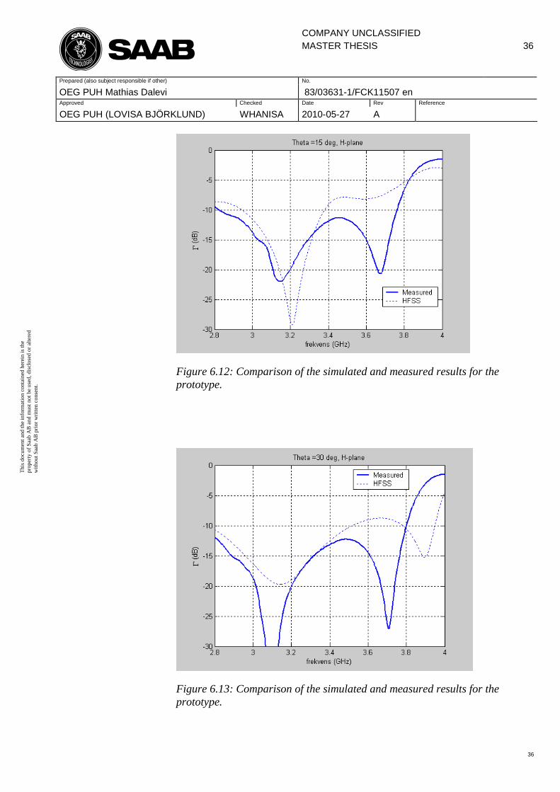
COMPANY UNCLASSIFIED
MASTER THESIS
36
Prepared (also subject responsible if other) No.
OEG PUH Mathias Dalevi 83/03631-1/FCK11507 en Approved Checked Date Rev Reference
OEG PUH (LOVISA BJÖRKLUND) WHANISA 2010-05-27 A
36
This
docu
men
t an
d t
he
info
rmat
ion c
onta
ined
her
ein i
s th
e
pro
per
ty o
f S
aab A
B a
nd m
ust
not
be
use
d,
dis
close
d o
r al
tere
d
wit
hout
Saa
b A
B p
rior
wri
tten
conse
nt.
Figure 6.12: Comparison of the simulated and measured results for the
prototype.
Figure 6.13: Comparison of the simulated and measured results for the
prototype.
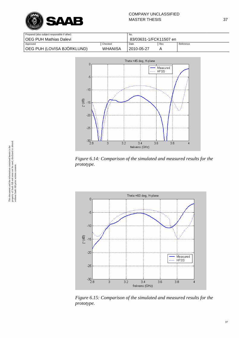
COMPANY UNCLASSIFIED
MASTER THESIS
37
Prepared (also subject responsible if other) No.
OEG PUH Mathias Dalevi 83/03631-1/FCK11507 en Approved Checked Date Rev Reference
OEG PUH (LOVISA BJÖRKLUND) WHANISA 2010-05-27 A
37
This
docu
men
t an
d t
he
info
rmat
ion c
onta
ined
her
ein i
s th
e
pro
per
ty o
f S
aab A
B a
nd m
ust
not
be
use
d,
dis
close
d o
r al
tere
d
wit
hout
Saa
b A
B p
rior
wri
tten
conse
nt.
Figure 6.14: Comparison of the simulated and measured results for the
prototype.
Figure 6.15: Comparison of the simulated and measured results for the
prototype.

COMPANY UNCLASSIFIED
MASTER THESIS
38
Prepared (also subject responsible if other) No.
OEG PUH Mathias Dalevi 83/03631-1/FCK11507 en Approved Checked Date Rev Reference
OEG PUH (LOVISA BJÖRKLUND) WHANISA 2010-05-27 A
38
This
docu
men
t an
d t
he
info
rmat
ion c
onta
ined
her
ein i
s th
e
pro
per
ty o
f S
aab A
B a
nd m
ust
not
be
use
d,
dis
close
d o
r al
tere
d
wit
hout
Saa
b A
B p
rior
wri
tten
conse
nt.
Figure 6.16: Comparison of the simulated and measured results for the
prototype.
Figure 6.17: Comparison of the simulated and measured results for the
prototype.

COMPANY UNCLASSIFIED
MASTER THESIS
39
Prepared (also subject responsible if other) No.
OEG PUH Mathias Dalevi 83/03631-1/FCK11507 en Approved Checked Date Rev Reference
OEG PUH (LOVISA BJÖRKLUND) WHANISA 2010-05-27 A
39
This
docu
men
t an
d t
he
info
rmat
ion c
onta
ined
her
ein i
s th
e
pro
per
ty o
f S
aab A
B a
nd m
ust
not
be
use
d,
dis
close
d o
r al
tere
d
wit
hout
Saa
b A
B p
rior
wri
tten
conse
nt.
Figure 6.18: Comparison of the simulated and measured results for the
prototype
Figure 6.19: Comparison of the simulated and measured results for the
prototype
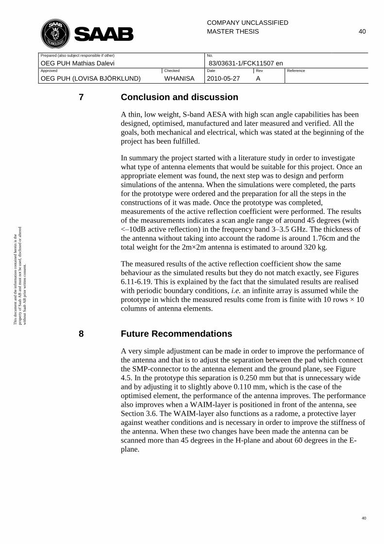
COMPANY UNCLASSIFIED
MASTER THESIS
40
Prepared (also subject responsible if other) No.
OEG PUH Mathias Dalevi 83/03631-1/FCK11507 en Approved Checked Date Rev Reference
OEG PUH (LOVISA BJÖRKLUND) WHANISA 2010-05-27 A
40
This
docu
men
t an
d t
he
info
rmat
ion c
onta
ined
her
ein i
s th
e
pro
per
ty o
f S
aab A
B a
nd m
ust
not
be
use
d,
dis
close
d o
r al
tere
d
wit
hout
Saa
b A
B p
rior
wri
tten
conse
nt.
7 Conclusion and discussion
A thin, low weight, S-band AESA with high scan angle capabilities has been
designed, optimised, manufactured and later measured and verified. All the
goals, both mechanical and electrical, which was stated at the beginning of the
project has been fulfilled.
In summary the project started with a literature study in order to investigate
what type of antenna elements that would be suitable for this project. Once an
appropriate element was found, the next step was to design and perform
simulations of the antenna. When the simulations were completed, the parts
for the prototype were ordered and the preparation for all the steps in the
constructions of it was made. Once the prototype was completed,
measurements of the active reflection coefficient were performed. The results
of the measurements indicates a scan angle range of around 45 degrees (with
<–10dB active reflection) in the frequency band 3–3.5 GHz. The thickness of
the antenna without taking into account the radome is around 1.76cm and the
total weight for the 2m×2m antenna is estimated to around 320 kg.
The measured results of the active reflection coefficient show the same
behaviour as the simulated results but they do not match exactly, see Figures
6.11-6.19. This is explained by the fact that the simulated results are realised
with periodic boundary conditions, i.e. an infinite array is assumed while the
prototype in which the measured results come from is finite with 10 rows × 10
columns of antenna elements.
8 Future Recommendations
A very simple adjustment can be made in order to improve the performance of
the antenna and that is to adjust the separation between the pad which connect
the SMP-connector to the antenna element and the ground plane, see Figure
4.5. In the prototype this separation is 0.250 mm but that is unnecessary wide
and by adjusting it to slightly above 0.110 mm, which is the case of the
optimised element, the performance of the antenna improves. The performance
also improves when a WAIM-layer is positioned in front of the antenna, see
Section 3.6. The WAIM-layer also functions as a radome, a protective layer
against weather conditions and is necessary in order to improve the stiffness of
the antenna. When these two changes have been made the antenna can be
scanned more than 45 degrees in the H-plane and about 60 degrees in the E-
plane.
COMPANY UNCLASSIFIED
MASTER THESIS
41
Prepared (also subject responsible if other) No.
OEG PUH Mathias Dalevi 83/03631-1/FCK11507 en Approved Checked Date Rev Reference
OEG PUH (LOVISA BJÖRKLUND) WHANISA 2010-05-27 A
41
This
docu
men
t an
d t
he
info
rmat
ion c
onta
ined
her
ein i
s th
e
pro
per
ty o
f S
aab A
B a
nd m
ust
not
be
use
d,
dis
close
d o
r al
tere
d
wit
hout
Saa
b A
B p
rior
wri
tten
conse
nt.
To make the simulated results more alike the measured results changes in the
model can be made in order to make the model more alike the prototype. One
change to make is to model the via-holes which enclose the feeding-structure
more accurate. One could also use more points in the simulation and further
increase the resolution.
These changes will make the model more complex and the time to simulate
will take much longer time.
References
[1] Skolnik Merrill L., Introduction to Radar Systems 3rd
edition.
McGraw-Hill Higher Education, 2001.
[2] Parker D, Zimmerman D. C., Phased arrays-part1: theory and
architectures. IEEE Transactions on Microwave Theory and
Techniques. Vol. 50, Issue 3:678–687, 2002.
[3] Balanis C. A., Antenna Theory, 3rd
edition. John Wiley & Sons, 2005.
[4] Tallini D, Galli A, Ciattaglia M, Infante L, De Luca A, Cicolani M., A
new low-profile wide-scan phased array for UWB applications.
Proceedings of Antennas and Propagation 2007. EuCAP 2007.
[5] Nikolic M. M, Djordjevic A. R, Nehorai A., Microstrip Antennas With
Suppressed Radiation in Horizontal Directions and Reduced Coupling.
IEEE Transactions on Antennas and Propagation. Vol. 53, No. 11, pp
3469–3475, November 2005.
[6] Magill E. G, Wheeler H. A., Wide-Angle Impedance Matching of a
Planar Array Antenna by a Dielectric Sheet. IEEE Transactions on
Antennas and propagation Volume 14, Issue 1:49 – 53, Jan. 1966.
[7] Skolnik, Merrill L., Radar Handbook (2nd
Edition). McGraw-Hill,
1990. Online version available at: http://knovel.com.proxy.lib.chalmers.se/web/portal/browse/display?_EXT_KNOVEL_DISPLAY_bookid=701&VerticalID=0. Accessed 2010-02-01.
COMPANY UNCLASSIFIED
MASTER THESIS
42
Prepared (also subject responsible if other) No.
OEG PUH Mathias Dalevi 83/03631-1/FCK11507 en Approved Checked Date Rev Reference
OEG PUH (LOVISA BJÖRKLUND) WHANISA 2010-05-27 A
42
This
docu
men
t an
d t
he
info
rmat
ion c
onta
ined
her
ein i
s th
e
pro
per
ty o
f S
aab A
B a
nd m
ust
not
be
use
d,
dis
close
d o
r al
tere
d
wit
hout
Saa
b A
B p
rior
wri
tten
conse
nt.
[8] Huss L-G, Gunnarsson R, Andersson P, Erickson R., A wideband,
wide angle scan, microstrip array antenna element. Proceedings of the
EURAD, 2005.
[9] Beenamole, K. S, Kutiyal, P. N. S, Revankar, U. K, Pandharipande
V.M., Compact planar microstrip antenna element for wide-scan angle
active phased arrays. Proceedings of Antennas and Propagation, 2007.
EuCAP 2007. pp 1-3.
[10] Waterhouse R., Small microstrip patch antenna. Electronics letters.
Vol. 31. No. 8, 1995.
[11] Holub, Alois, Polívka, Milan., A novel microstrip patch antenna
miniaturization technique: A meanderly folded shorted-patch.
Microwave Techniques. Vol. 23-24. pp. 1-4, 2008.
[12] Chair, R., Lee, K. F., Luk. K. M., Bandwidth and cross-polarization
characteristics of quarter-wave shorted patch antennas. Microwave and
optical technology letters. Vol. 22, No. 2, 1999.
[13] Svennson, B., Lanne, M., Verification of an active phased array using
single element measurments. First AMTA Europe Symposium, 2006.

COMPANY UNCLASSIFIED
MASTER THESIS
43
Prepared (also subject responsible if other) No.
OEG PUH Mathias Dalevi 83/03631-1/FCK11507 en Approved Checked Date Rev Reference
OEG PUH (LOVISA BJÖRKLUND) WHANISA 2010-05-27 A
43
This
docu
men
t an
d t
he
info
rmat
ion c
onta
ined
her
ein i
s th
e
pro
per
ty o
f S
aab A
B a
nd m
ust
not
be
use
d,
dis
close
d o
r al
tere
d
wit
hout
Saa
b A
B p
rior
wri
tten
conse
nt.
Appendix
A.1 Material
Table A.1: Table shows the properties of some of the different material
which were considered during the project.
Material εr Dissipation loss factor tan(δ)@10GHz
Density [g/cm
3]
Coefficient of thermal expansion(x)
Coefficient of thermal expansion(y)
Coefficient of thermal expansion(z)
FR-4 4.8 1.9
Roger4350B 3.48 0.0037 1.86 14 16 35
Rogers4003C 3.38 0.0027 1.79 11 14 46
Rogers4450B 3.54 0.004 1.86 19 17 50
RT/Duroid 5880
2.2 0.0009 2.2
Rohacell 71 HF
1.09 0.0038 0.075
Copper 1 0 8.94 16.7 16.7
A.2 Connector
The SMP-connector used for the prototype is called rpt368405/3. The regular
footprints for the connector can be used.

COMPANY UNCLASSIFIED
MASTER THESIS
44
Prepared (also subject responsible if other) No.
OEG PUH Mathias Dalevi 83/03631-1/FCK11507 en Approved Checked Date Rev Reference
OEG PUH (LOVISA BJÖRKLUND) WHANISA 2010-05-27 A
44
This
docu
men
t an
d t
he
info
rmat
ion c
onta
ined
her
ein i
s th
e
pro
per
ty o
f S
aab A
B a
nd m
ust
not
be
use
d,
dis
close
d o
r al
tere
d
wit
hout
Saa
b A
B p
rior
wri
tten
conse
nt.
A.3 Radar bands
Table A.3: The definition of the radar-bands according to IEEE definitions.
From Balanis, 2005 [3].