Embed Size (px)
Citation preview
- .
REPORT NO. 29169-11
STUDY OF I S T E P RECOVERY DIODE I
I FREQUENCY M U L T I P L I E R CHARACTERISI'ICS
R Y A N
Hard COPY
Microfiche
if 653 Julv 65
Q 3 : e =!
13 I
https://ntrs.nasa.gov/search.jsp?R=19680019939 2018-05-18T02:33:27+00:00Z
REPORT NO. 29169-11
STUDY OF
S T E P RECOVERY DIODE
FREQUENCY M U L T I P L I E R CHARACTERISTICS
INTERIM REPORT NO. 3
FEBRUARY 1968
CONTRACT NAS 8-20257
Prepared f o r
GEORGE C. MARSHALL SPACE FLIGHT CENTER
Prepared by
RYAN AERONPJJTICAL COMPANY
ELECTRONIC AND SPACE SYSTEMS
5650 KEARNY MESA ROAD
SAN DIEGO, CALIFORNIA 92112

4
ABSTRACT
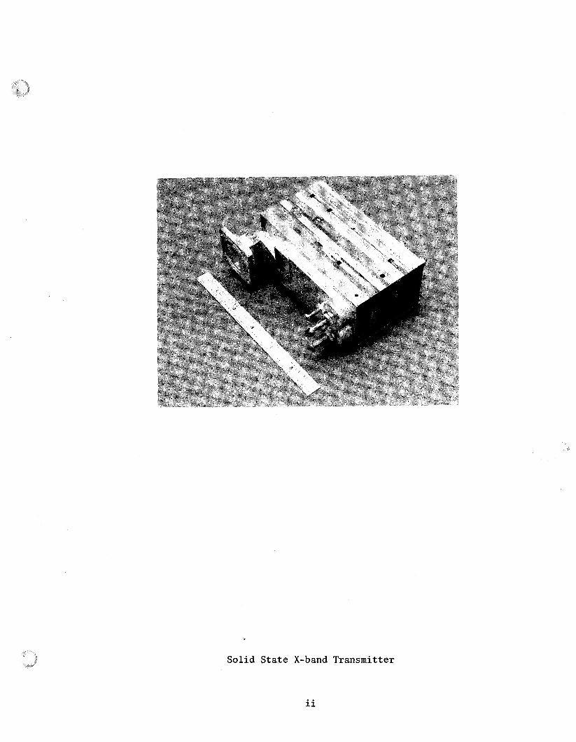
This report describes the design and tests of a compact so l id-s ta te , X-Band
Transmitter (SSX) using s t e p recovery diode (SRD) mult ip l ie rs . Increased X-band output power is obtained by p a r a l l e l connecting outputs of two multi-
p l i e r s tages .
ing r e su l t s .
Limited environmental tests were performed and yielded promis-
I
i
r
Solid S ta t e X-band Transmitter
ii
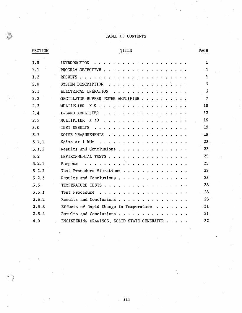
TABLE OF CONTENTS
SECTION TITLE . PAGE
1.0
1.1 1 . 2
2 .0
2 . 1
2 . 2
2 . 3
2 .4
2 .5
3 . 0
3 . 1
3 . 1 . 1
3 . 1 . 2
3 . 2
3 . 2 . 1
3 . 2 . 2
3 . 2 . 3
3 . 3
3 . 3 . 1
3 . 3 . 2
3 . 3 . 3
3 . 3 . 4
4 .0
INTRODUCTION . . . . . . . . . . . . . . . . . . . . PROGRAM OBJECTIVE . . . . . . . . . . . . . . . . . . RESULTS . . . . . . . . . . . . . . . . . . . . . . . SYSTEM DESCRIPTION . . . . . . . . . . . . . . . . . ELECTRICAL OPERATION . . . . . . . . . . . . . . . . OSCILLATOR-BUFFER POWER AMPLIFIER . . . . . . . . . . MULTIPLIER X 9 . . . . . . . . . . . . . . . . . . . L-BAND AMPLIFIER . . . . . . . . . . . . . . . . . . MULTIPLIER X 1 0 . . . . . . . . . . . . . . . . . . TESTRESULTS . . . . . . . . . . . . . . . . . . . . NOISE MEASUREMENTS . . . . . . . . . . . . . . . . . Noise at 1 kHz . . . . . . . . . . . . . . . . . . . Results and Conclusions . . . . . . . . . . . . . . . ENVIRONMENTAL TESTS . . . . . . . . . . . . . . . . . Purpose . . . . . . . . . . . . . . . . . . . . . . Test Procedure Vibrations . . . . . . . . . . . . . . . Results and Conclusions . . . . . . . . . . . . . . . TEMPERATURE TESTS . . . . . . . . . . . . . . . . . . Test Procedure . . . . . . . . . . . . . . . . . . . Results and Conclusions . . . . . . . . . . . . . . . Effects of Rapid Change in Temperature . . . . . . . Results and Conclusions . . . . . . . . . . . . . . . ENGINEERING DRAWINGS. SOLID STATE GENERATOR . . . . .
1
1
1 3
3
7 10
12
15
19
19
23 . 23
25
25
25
25
28
28
28
31
31
32
iii
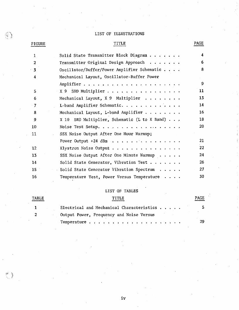
LIST OF ILLUSTRATIONS
FIGURE
5
6
7
8
9
10
11
12
13
14
15
16
TABLE
1 2
TITLE
Sol id S t a t e Transmitter Block Diagram . . . . . . Transmitter Original Design Approach . . . . . . . Oscillator/Buffer/Power Amplifier Schematic . . . Mechanical Layout, Osci l la tor-Buffer Power
A m p l i f i e r . . . . . . . . . . . - . . . . . . . . X 9 SRD Mul t ip l ie r . . . . . . . . . . a . . * . . Mechanical Layout, X 9 Mul t ip l i e r . . . e . . . . L-band Amplifier Schematic. . . . . . . . . . . . . Mechanical Layout, L-band Amplifier . . e . . . . X 10 SRD Mul t ip l ie r , Schematic (L t o X Band) a a . Noise Test Setup. . . . . . a . . . . ... . . . . SSX Noise Output After One Hour Warmup;
Power Output +24 dBm . . . . . . . . . . . . . . Klystron Noise Output . . . . . . e . . - e . e . SSX Noise Output After One Minute Warmup . . a . Solid S t a t e Generator, Vibration T e s t . . . . . Sol id S t a t e Generator Vibration Spectrum . . . Temperature Test, Power Versus Temperature . . . .
LIST OF TABLES
TITLE
Electrical and Mechanical Charac te r i s t ics . . . . . Output Power, Frequency and Noise Versus
Temperature . . . . . . . . . . . . . e a . . . .
PAGE
9
11
13
14
16
18
20
21
22
24
26
27
30
PAGE
5
-
29
SECTION 1
INTRODUCTION
Ryan Electronic and Space Systems, a f a c i l i t y of t he Ryan Aeronautical
Company, is present ly inves t iga t ing the applications of Step Recovery
Diodes (SRD's) i n t h e microwave region. The program i s supported by the
Marshall Space Fl ight Center, Huntsvil le, Alabama, under contract
NAS-8-20257. During t h i s invest igat ion, an experimental SRD mul t ip l i e r ' operating a t an output frequency i n the X-band was constructed and given
. . .. ~-~ ~
preliminary tests.
s t a b l e and contained less noise than the output from an X-band klystron. .- -
Power output o f the mul t ip l i e r was l imited by t h e avai lable diodes.
These tests showed t h a t the X-band output w a s very . - _- --
1.1 PROGRAM OBJECTIVE
The pr inc ipa l object ive was t o perform studies and experimental investiga-
t i o n i n the design of s o l i d state X-band transmitters employing Step- recovery diode (SRD) mul t ip l ie rs .
1 . 2 RESULTS
A s o l i d s t a t e t ransmi t te r w a s designed and b u i l t .
investigated; t he one se lec ted uses two SRD mul t ip l ie rs .
Two approaches were
The generator was t e s t e d for output power and noise under various environ- mental conditions.
This interim report describes the methods o f construction and the r e s u l t s
of t h e tests of the generator. The work described i n t h i s report is only
a pa r t of t h e overa l l development and implementation of the appl icat ion of
SRD's a t Ryan. This work is a continuing e f f o r t and is being described i n a regular series of progress reports .
1
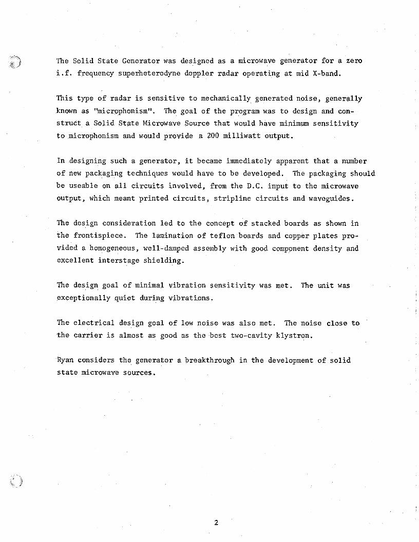
The Sol id S ta t e Generator was designed as a microwave generator f o r a zero
i.f. frequency superheterodyne doppler radar operating at mid X-band.
This type o f radar i s sens i t i ve t o mechanically generated noise, generally
known as "microphonism".
s t r u c t a Sol id S ta t e Microwave Source t h a t would have minimum s e n s i t i v i t y
t o microphonism and would provide a 200 m i l l i w a t t output.
The goal of the program was t o design and con-
In designing such a generator, it became immediately apparent t h a t a number
o f new packaging techniques would have t o be developed.
be useable on a l l c i r c u i t s involved, from the D.C. input t o the microwave
output, which meant pr in ted c i r c u i t s , s t r i p l i n e circuits and waveguides.
The packaging should
The design consideration l ed t o the concept of stacked boards as shown i n
the front ispiece. The lamination of t e f lon boards and copper p l a t e s pro- vided a homogeneous, well-damped assembly with good component densi ty and
excel lent in te rs tage shielding.
The design goal of minimal vibrat ion s e n s i t i v i t y was m e t .
exceptionally quie t during vibrat ions.
The un i t w a s
The electrical design goal of low noise was a l so met.
t h e c a r r i e r is almost as good as the bes t two-cavity klystron.
The noise c lose t o
Ryan considers the generator a breakthrough i n t h e development of s o l i d
s ta te microwave sources.
2
P SECTION 2
SYSTEM DESCRIPTION
2 . 1 ELECTRICAL OPERATION
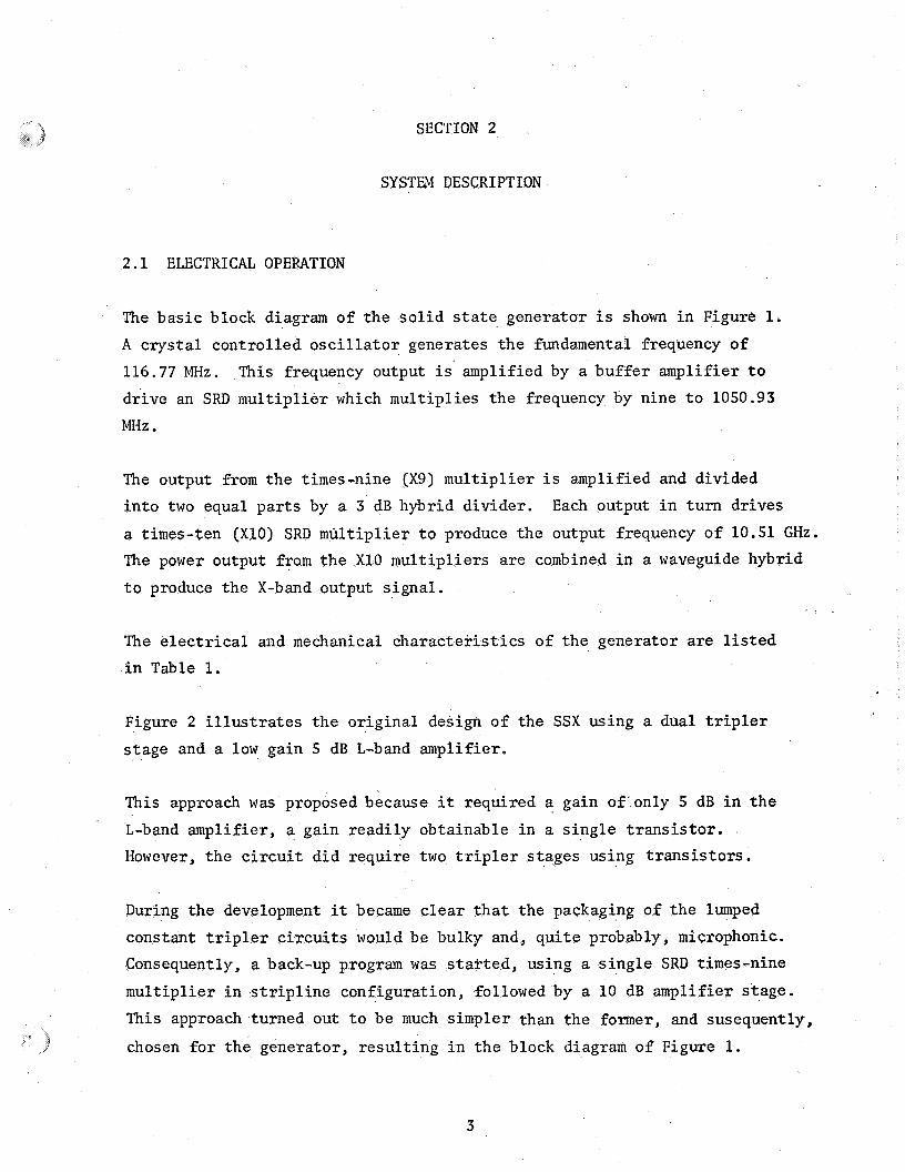
The bas i c block diagram of t h e s o l i d s ta te generator is shown i n Figure 1. A c rys t a l control led o s c i l l a t o r generates t he fundamental frequency of 116.77 MHz.
dr ive an SRD mul t ip l i e r which mult ipl ies t he frequency by nine t o 1050.93
MHz .
This frequency output i s amplified by a bu f fe r amplif ier t o
The output from the times-nine (X9) mul t ip l i e r i s amplified and divided
i n t o two equal pa r t s by a 3 dB hybrid divider .
a times-ten (X10) SRD mul t ip l i e r t o produce the output frequency o f 10.51 GHz. The power output from t h e X10 mul t ip l ie rs are combined i n a waveguide hybrid
t o produce t h e X-band output s ignal .
Each output i n turn drives
The e l e c t r i c a l and mechanical charac te r i s t ics of t h e generator are l i s t e d
i n Table 1.
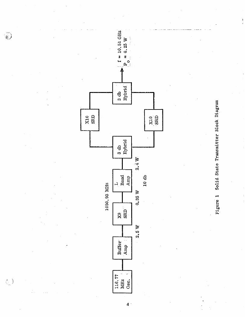
Figure 2 illustrates t h e or ig ina l design o f the SSX using a dual t r i p l e r s tage and a low gain 5 dB L-band amplifier.
This approach was proposed because it required a gain of only 5 dB i n t h e
L-band amplifier, a gain readi ly obtainable i n a s ing le t r ans i s to r .
However, t h e c i r c u i t d id require two t r i p l e r s tages using t r ans i s to r s .
During the development it became clear t h a t the packaging of t h e lumped
constant t r i p l e r c i r c u i t s would be bulky and, qu i t e probably, microphonic.
Consequently, a back-up program was s t a r t e d , using a s ing le SRD times-nine
mul t ip l ie r i n s t r i p l i n e ccnfiguration, followed by a 10 dB amplif ier s tage. This approach turned out t o be much simpler than the former, and susequently,
chosen f o r t h e generator, resu l t ing i n t h e block diagram of Figure 1.
3
i
k Q) c, c,
4
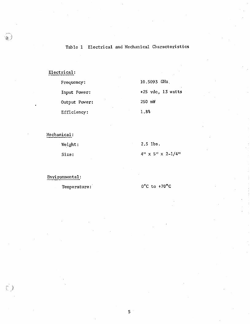
Table 1 Electrical and Mechanical Charac t e r i s t i c s
Electrical :
Frequency :
Input Power :
Output Power :
Efficiency :
Mechanical :
Weight :
Size:
Environmental :
Temperature :
10.5093 GHz,
+25 vdc, 13 watts
250 mW
1.8%
2.5 l b s .
4" x S" x 2-1/41'
O°C t o +7OoC
5
6
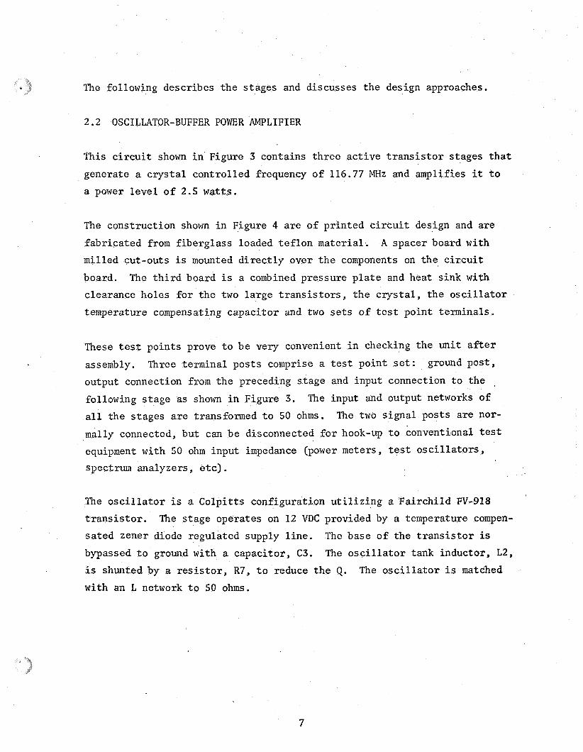
The following describes t h e s tages and discusses the design approaches.
2 . 2 OSCILLATOR-BUFFER POWER AMPLIFIER
This c i r c u i t shown i n Figure 3 contains three active t r a n s i s t o r stages t h a t
generate a crystal control led frequency of 116.77 MHz and amplifies it t o
a power level o f 2.5 watts.
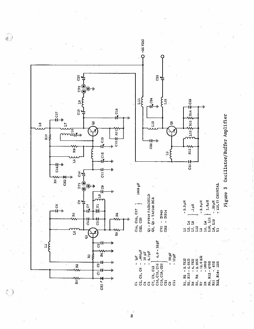
The construction shown i n Figure 4 are of pr in ted c i r c u i t design and are fabricated from f iberg lass loaded t e f lon mater ia l . milled cut-outs is mounted d i r e c t l y over t h e components on the c i r c u i t
board.
clearance holes f o r t he two large t r ans i s to r s , t h e c rys t a l , t he o s c i l l a t o r
temperature compensating capaci tor and two sets o f tes t point terminals.
A spacer board with
The t h i r d board i s a combined pressure p l a t e and heat sink with
These tes t points prove t o be very convenient i n checking the uni t after assembly. ground post , Three terminal posts comprise a t e s t point s e t :
output connection from the preceding s tage and input connection t o the
following s tage as shown i n Figure 3.
a l l t he s tages are transformed t o 50 ohms. The two s igna l posts are nor-
mally connected, but can be disconnected fo r hook-up t o conventional tes t equipment with 50 ohm input impedance (power meters, test o s c i l l a t o r s ,
The input and output networks o f
spectrum analyzers, ete) .
The o s c i l l a t o r is a Colp i t t s configuration u t i l i z i n g a Fa i rch i ld FV-918
t r a n s i s t o r .
sa ted zener diode regulated supply l i ne .
bypassed t o ground with a capacitor, C 3 .
is shunted by a r e s i s t o r , R7, t o reduce the Q.
with an L network t o 50 ohms.
The s tage operates on 1 2 VDC provided by a temperature compen-
The base of the t r a n s i s t o r is The o s c i l l a t o r tank inductor, L2,
The o s c i l l a t o r i s matched
7
H VJ N
I '
ih
% k r l a
3% I 1 1
2 2 v v
(0
V m u
?i aa n
c:
. .
8
a b C
Figure 4 Mechanical Layout, Oscillator-Buffer Power Amplifier
9
The c rys t a l i s a series resonance un i t mounted i n a TO-5 t r a n s i s t o r can.
The s t r a y capacity across t h e c rys t a l is resonated with an inductor, L3.
A temperature compensating capaci tor , CS, connected across the crystal provides a temperature tracking correct ion o f approximately 10%.
o s c i l l a t o r del ivers 10 m i l l i w a t t s .
The
The buffer amplif ier uses an RCA 2N5090 t r a n s i s t o r i n a neutral ized common
emitter configuration. The gain o f t h i s s tage is 14 dB. This y ie lds a power output of 260 milliwatts when driven by the 10 m i l l i w a t t s from the
o s c i l l a t o r .
at tenuation.
temperature var ia t ion of the emitter-base junction. c i r c u i t u t i l i z e s a T network.
work.
and simple.
effect on the o s c i l l a t o r .
Neutralization provides approximately 35 t o 40 dB reverse
A diode, CR2, i s used i n the b i a s c i r c u i t t o compensate f o r
The input matching
The output matching c i r c u i t uses an L net-
Through use o f the t e s t points neut ra l iza t ion i s straightforward This neut ra l ized buf fer s tage reduces output load var ia t ions
The power amplif ier s tage a l so uses an RCA 2N5090 t r a n s i s t o r i n a common
emi t te r unneutralized configuration.
network and the output matching c i r c u i t i s an L network.
provides 10 dB power gain which del ivers 2.5 watts a t 116.77 MHz i n t o a 50 ohm load.
+25 VDC.
The input matching c i r c u i t i s a T This s tage
Total current f o r the board is approximately 0.12 A, a t
2.3 MULTIPLIER X9
The o s c i l l a t o r buffer amplif ier provides an output of 2 watts a t 116.77 MHz t o dr ive the X9 mult ip l ie r .
t he ninth harmonic zt 1050.93 PWz. i s 17.5% which y ie lds an output o f 350 m i l l i w a t t s .
This s t e p recovery diode mul t ip l ie r generates
The power eff ic iency of t he mul t ip l i e r
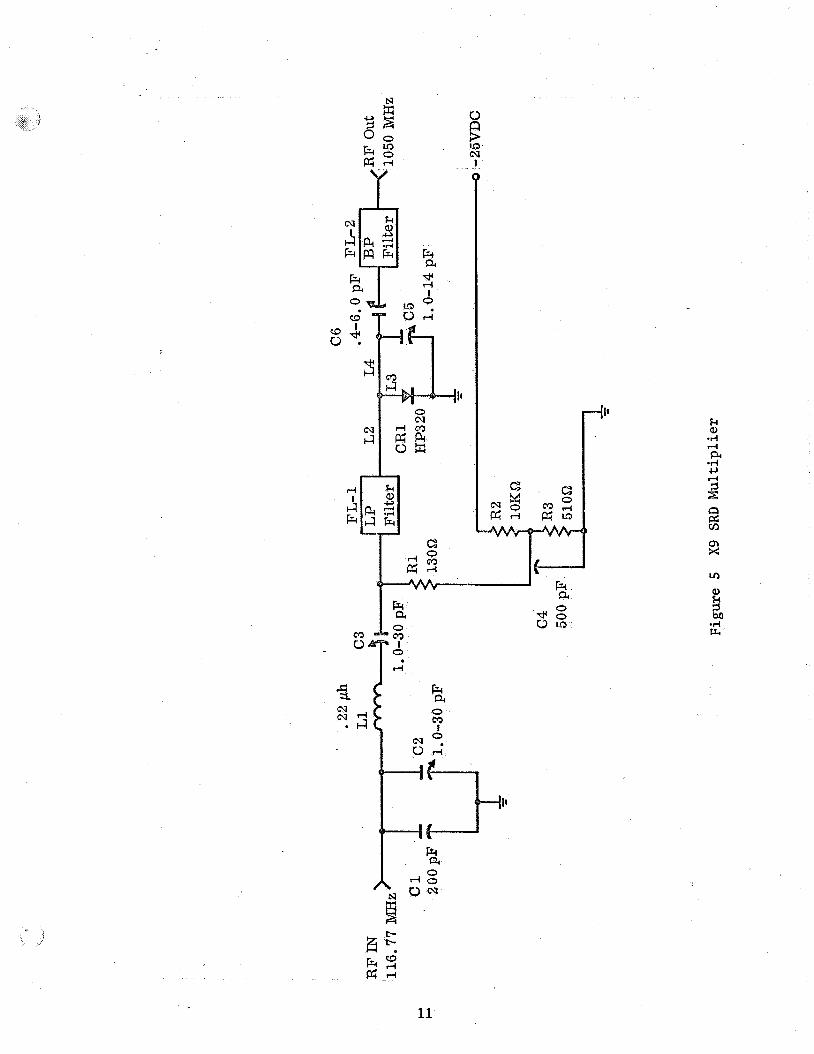
A c i r c u i t diagram of the X9 mult ip l ie r i s shown i n Figure 5.
recovery diode is an HPA 0320, which was se lec ted on the bas i s o f required
power output, input and output frequencies, and the diode's reverse b i a s
capacitance.
The s t ep
10
f
k 0 M
I 0
4
The mul t ip l ie r i s a shunt c i r c u i t using lumped c i r c u i t elements a t the
input frequency and s t r i p l i n e circuit elements at the output frequency.
A combination o f self and f ixed b i a s f o r proper operation of t he SRD is supplied by the b i a s network consis t ing of R1, R2, R3, and C4.
mission l i ne choke (FL-1) prevents t h e ninth harmonic from flowing back
i n t o the input c i r c u i t .
resonated by C5 and C6 t o optimize the power efficiency.
A trans-
Components L2, L3, L4 are s t r i p l i n e inductances
The input impedance is matched fo f i f t y ohms by C1 , C 2 , C3 and L 1 .
i n t e r d i g i t a l bandpass f i l t e r (FL-2) i n t h e output suppresses a l l harmonics
except the desired ninth harmonic.
Figure 6 .
An
The mechanical layout is shown in
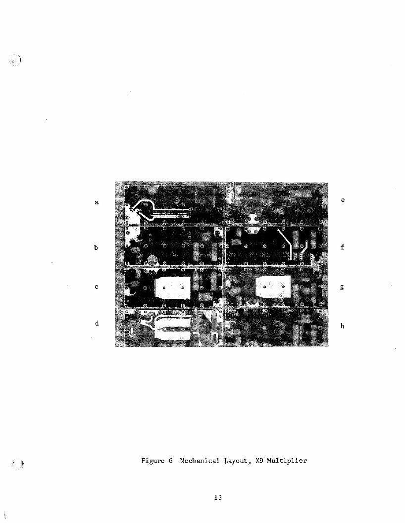
The eight s t r i p l i n e pr in ted c i r c u i t boards comprising the X9 SRD Mult ipl ier
are shown i n Figure 6.
Figure 6d.
FL-1.
i n Figures 6c and 6g.
l i nes i n Figure 6a.
t o provide spaces between the major c i r c u i t boards.
i n the d i e l e c t r i c t o accept piston-type adjustable capacitors with access
allowed f o r adjustment through s l o t s t o the board edges.
Most of the mul t ip l i e r c i r c u i t is i l l u s t r a t e d i n
The two wide s t r i p s i n the center comprise the input choke, -
The ground planes of t h i s choke are the wide a rea cent ra l ly located
The i n t e r d i g i t a l f i l t e r i s formed by the p a r a l l e l
Figures 6b, 6e, and 6f are d i e l e c t r i c spacers used
Slo ts are milled
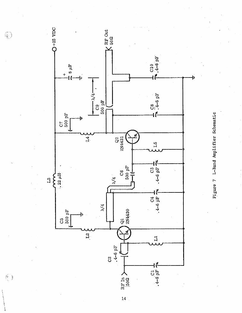
2.4 L-BAND AMPLIFIER
The L-band amplif ier shown i n Figure 7 receives the 350 m i l l i w a t t 1050.93
MHz s igna l from the X9 mult ip l ie r and amplifies it t o approximately 2.4 watts required t o dr ive t h e XI0 mul t ip l ie r .
emitter Class C s tages , a 2N4430 dr iver and a 2N4431 power amplifier.
matching networks are s t r i p l i n e d i s t r ibu ted circuits. capacitors are u t i l i z e d for c i r c u i t tuning.
The amplif ier consis ts o f two common
A l l
Johannson var iable
12
a
b
Figure 6 Mechanical Layout, X9 Mult ipl ier
13
e
A
14
Components L1, L2 , L3, L4 and LS are RF chokes.
resonate the input t o Q1 which i s a shortened quarter-wave sect ion.
two-section quarter-wave transformer is used t o s t e p up the co l l ec to r
impedance o f Q1 from 10 t o 150 ohms
by C5.
C 1 and C2 are used t o
A
t o t he input of 42 which i s resonated
The capacit ive reactance of C4 is presented as an inductive reactance t o
the co l lec tor of Q1 through a quarter-wave transformer.
42 is tuned by t h e equivalent of a double-stub tuner.
shunt and the combination o f C10 and a length o f l i n e s l i g h t l y grea te r than
X/4 is an inductive shunt; C9 is a DC block only.
The co l l ec to r of
C8 is a capaci t ive
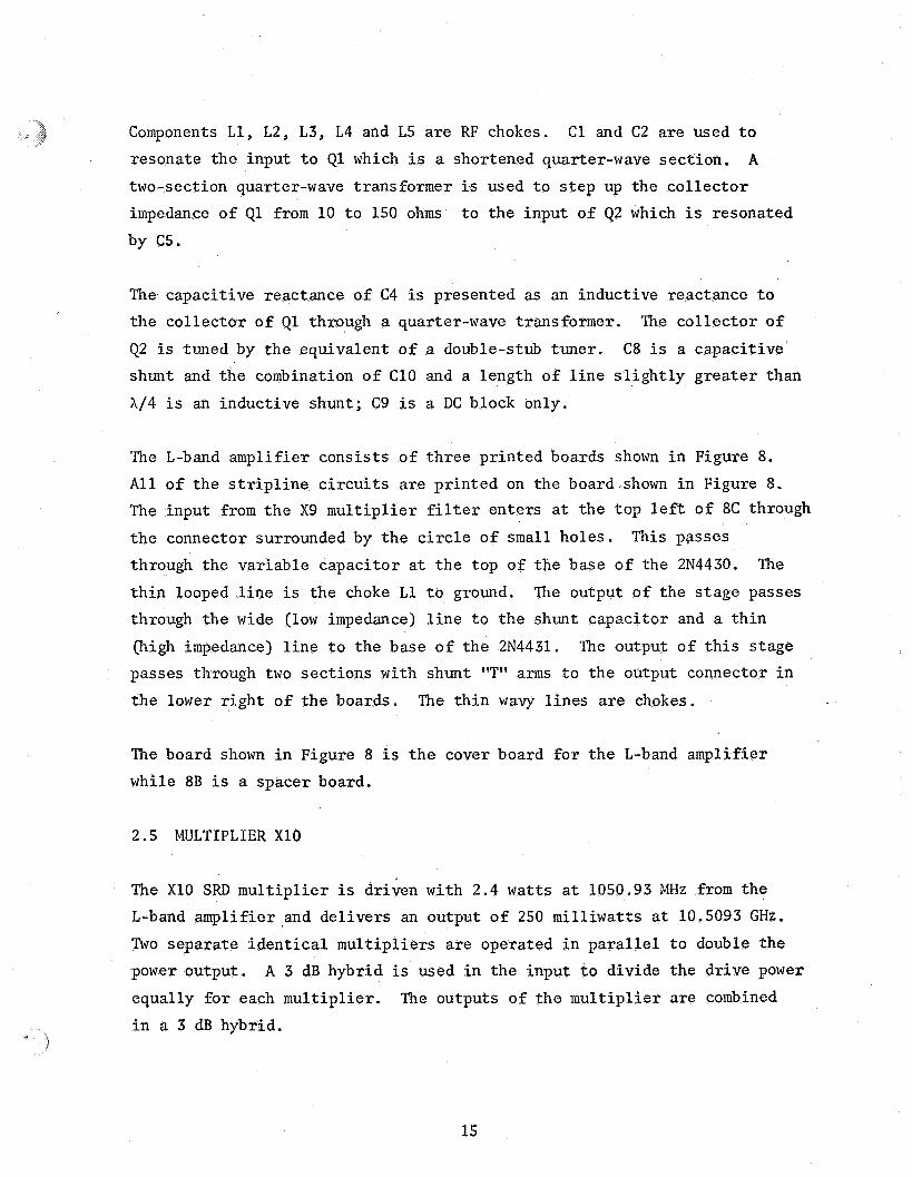
The L-band amplif ier consis ts o f th ree pr in ted boards shown i n Figure 8.
A l l of t h e s t r i p l i n e c i r c u i t s are pr in ted on the board shown i n Figure 8.
The input from t h e X9 mul t ip l ie r f i l t e r en ters a t t he top l e f t o f 8C through
t h e connector surrounded by t h e circle of small holes.
through the var iable capaci tor at t he top of the base o f the 2N4430.
t h i n looped l i n e i s the choke L l t o ground. through the wide (low impedance) l i n e t o the shunt capacitor and a th in
(high impedance) l i n e t o the base o f t he 2N4431. The output of t h i s s tage
passes through two sect ions with shunt "T" arms t o the output connector i n
the lower r igh t of the boards.
This passes
The
The output of the s tage passes
The t h i n wavy l ines are chokes.
The board shown i n Figure 8 i s t h e cover board for t h e L-band amplif ier
while 8 B is a spacer board.
2.5 MULTIPLIER X10
The X10 SW mult ip l ie r is driven with 2.4 watts a t 1050.93 MHz from the
L-band amplif ier and del ivers an output of 250 milliwatts a t 10.5093 GHz.
Two separate iden t i ca l mul t ip l ie rs are operated i n p a r a l l e l t o double the
power output.
equally for each mul t ip l ie r .
i n a 3 dB hybrid.
A 3 dB hybrid is used i n the input t o divide the dr ive power
The outputs of t he mul t ip l i e r are combined
15
a b C
Figure 8 Mechanical Layout, L-band Amplifier
16
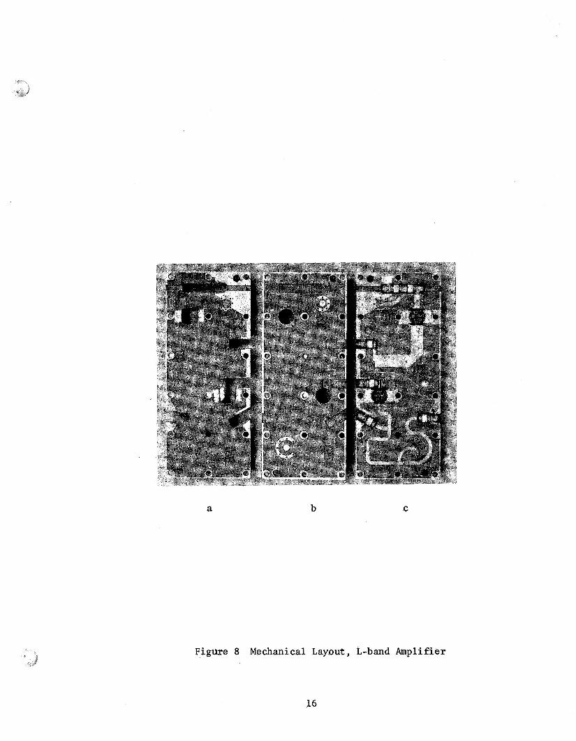
The input c i rcu i t shown i n Figure 9 consis ts o f a s t r i p l i n e hybrid power
divider . The combination o f C3 and C4 i n one arm and C5 and C6 i n the
other arm, each with a shortened X/4 transmission l i n e serve t o transform
t o a su i t ab le impedance f o r t he mul t ip l i e r diodes CR1 and CR2. Capacitors C8 and C9 are tuning capacitors a t t h e input frequency and serve as r a d i a l
chokes a t t h e input frequency.
The s t e p recovery diodes, CR1 and CR2 are coupled t o resonant X-band cav i t i e s
milled i n an aluminum block.
point by a zener diode and an appropriate voltage divider.
The SRD's are biased t o t he correct operating
Output from each mul t ip l i e r resonant cavi ty i s coupled t o separate arms of an X-band side-wall coupler connected as a 3 dB hybrid. This coupler com- bines t h e output of both mul t ip l ie rs i n t o a s ing le X-band waveguide output
connector.
17
++
0
2
SECTION 3
TEST RESULTS
The s o l i d state generator was t e s t ed f o r noise, vibrat ion and temperature.
The t e s t i n g i s described below.
3.1 NOISE MEASUREMENTS
The purpose of t h i s t e s t was t o measure t h e noise between 1 kHz and 100 kHz
from t h e ca r r i e r .
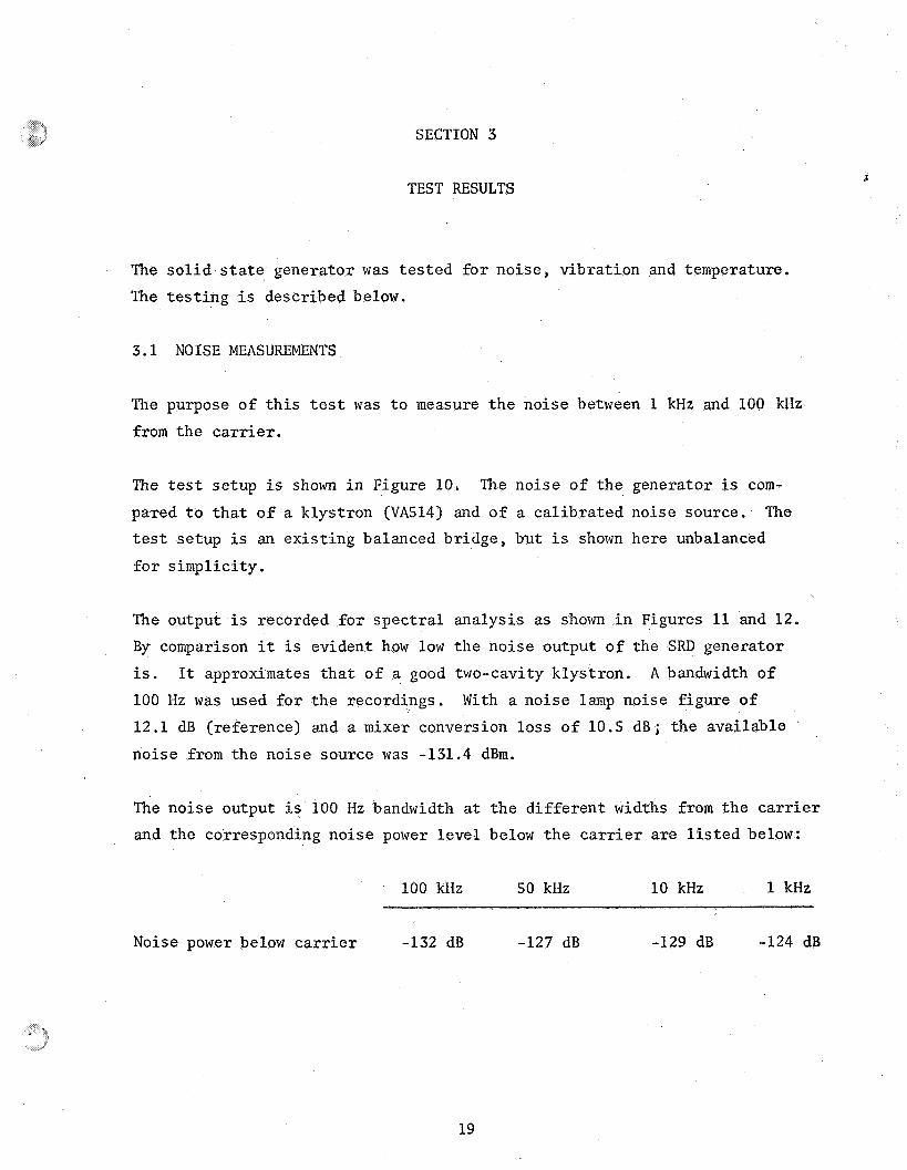
Tne test setup is shown i n Figure 10.
pared t o t h a t of a klystron (VA514) and of a ca l ibra ted noise source. The tes t setup is an ex is t ing balanced bridge, but i s shown here unbalanced
f o r s implici ty .
The noise of t h e generator is com-
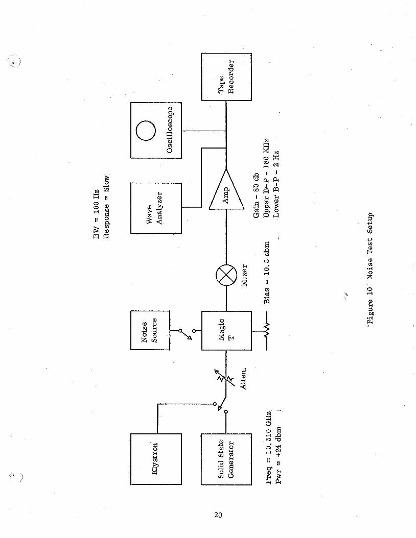
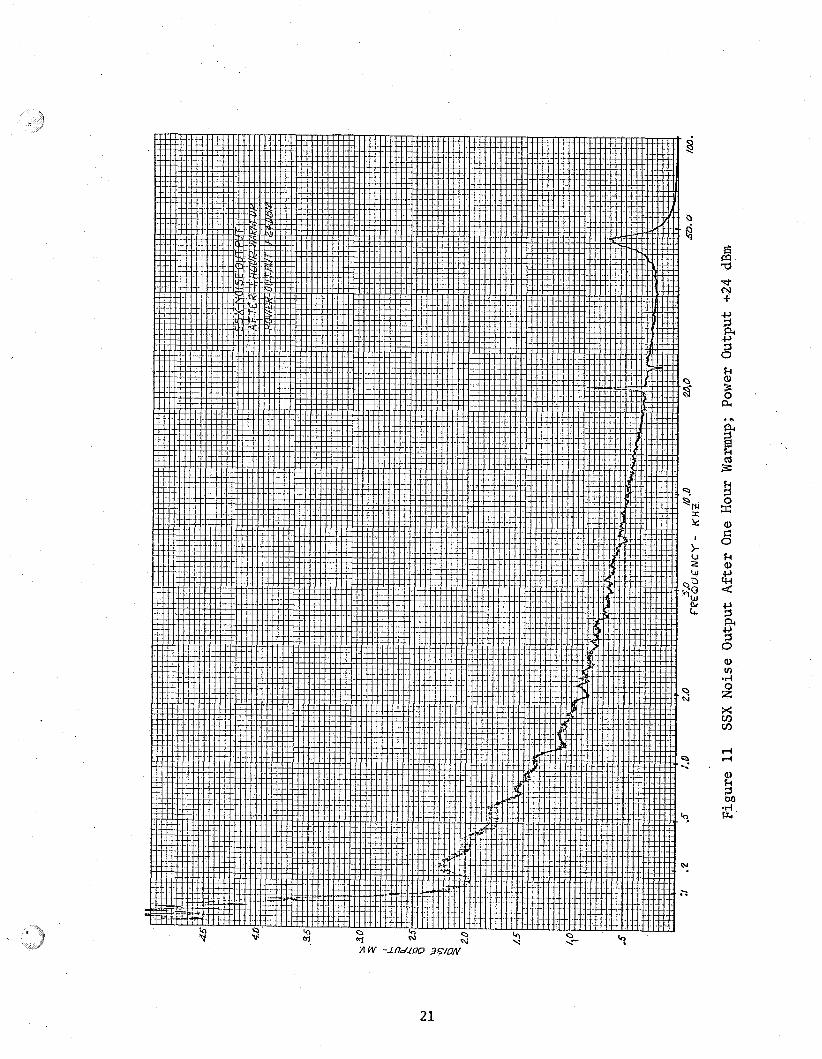
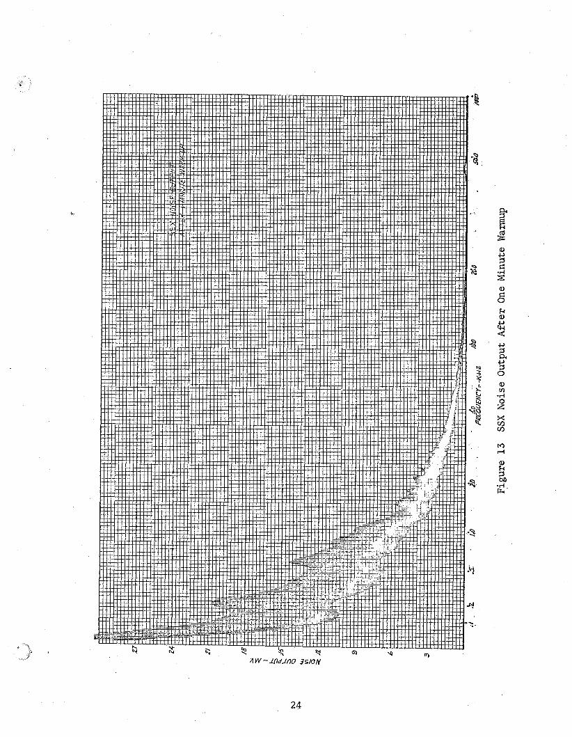
The output i s recorded f o r spec t r a l analysis as shown i n Figures 11 and 12 ,
By comparison it is evident how low the noise output o f the SRD generator
i s .
100 Hz was used f o r t he recordings.
1 2 . 1 dB (reference) and a mixer conversion loss o f 10.5 dB; the avai lable
noise from the noise source was -131.4 dBm.
I t approximates t h a t o f a good two-cavity klystron. A bandwidth of
With a noise lamp noise f igure of
The noise output i s 100 Hz bandwidth a t t h e d i f f e ren t widths from the carrier and the corresponding noise power leve l below t h e c a r r i e r are l i s t e d below:
100 kHz 50 kHz 10 kHz 1 kHz
Noise power below carrier -132 dB -127 dB -129 dB -124 dB
19
20
2 1
22
\
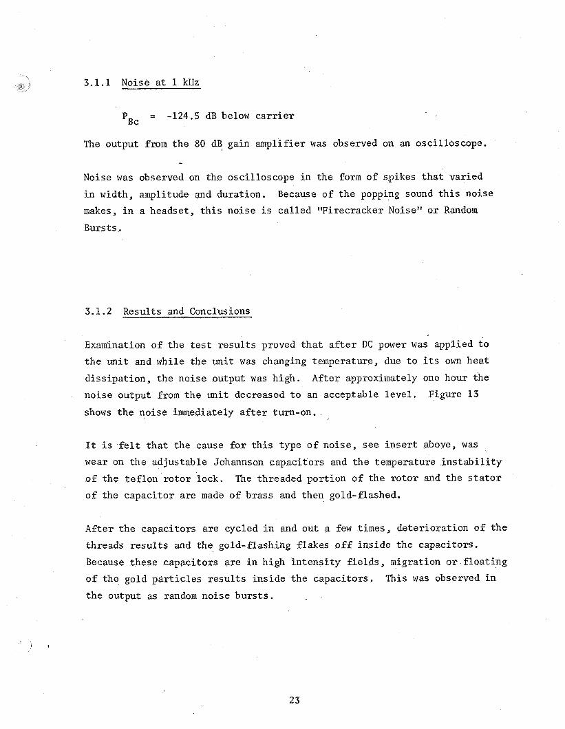
a i 3.1.1 Noise a t 1 kHz
= -124.5 dB below carrier pBC
The output from t h e 80 dB gain amplifier was observed on an oscil loscope.
- Noise was observed on the oscil loscope i n the form of spikes t h a t varied
i n width, amplitude and duration.
makes, i n a headset, t h i s noise is ca l led !!Firecracker Noise" o r Random
Bursts .
Because of t he popping sound t h i s noise
3.1.2 Results and Conclusions
Examination of t he t e s t r e su l t s proved t h a t a f t e r DC power was applied t o
t h e uni t and while t he uni t was changing temperature, due t o i t s own heat
d i ss ipa t ion , t he noise output was high. After approximately one hour the
noise output from t h e un i t decreased t o an acceptable leve l .
shows t h e noise immediately a f t e r turn-on.
Figure 13
I t i s f e l t t h a t the cause fo r t h i s type of noise , see i n s e r t above, was wear on t h e adjustable Johannson capacitors and the temperature i n s t a b i l i t y
of the te f lon ro to r lock. The threaded port ion of the ro to r and t h e s t a t o r
o f the capaci tor are made of brass and then gold-flashed.
After t h e capacitors are cycled i n and out a few times, de te r iora t ion of t h e
threads r e su l t s and the gold-flashing f lakes of f i n s ide the capacitors.
Because these capacitors a re i n high in t ens i ty f i e l d s , migration o r f loa t ing
o f the gold pa r t i c l e s r e s u l t s ins ide the capaci tors .
t he output as random noise burs t s .
This was observed i n
23
6) F: 0 k 6)
2
3.2 ENVIRONMENTAL TESTS
3 .2 .1 Purpose
The purpose o f these t e s t s was t o examine the low frequency vibrat ional
cha rac t e r i s t i c s and t h e temperature cha rac t e r i s t i c s o f the s o l i d s ta te
generator.
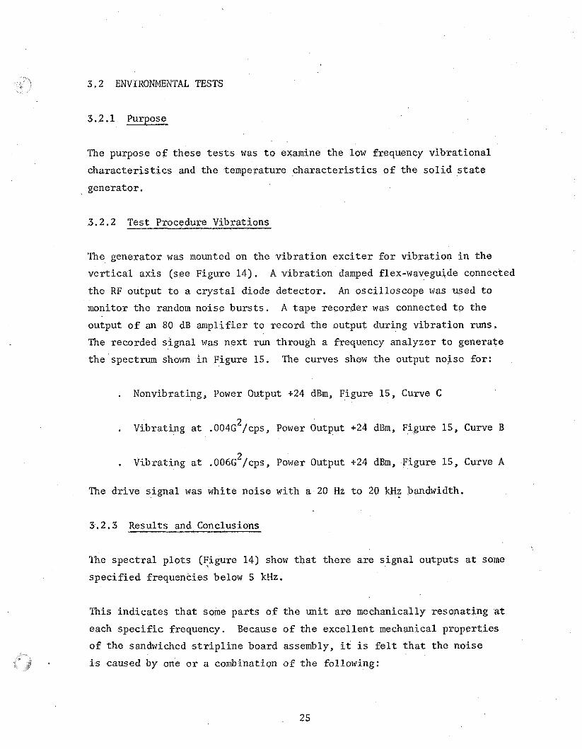
3.2.2 Test Procedure Vibrations
The generator was mounted on the vibrat ion exc i t e r f o r vibrat ion i n the
ve r t i ca l axis (see Figure 14). A vibrat ion damped flex-waveguide connected
the RF output t o a c rys t a l diode detector .
monitor t he random noise bu r s t s .
output o f an 80 dB amplif ier t o record t h e output during vibrat ion runs.
The recorded s ignal was next run through a frequency analyzer t o generate
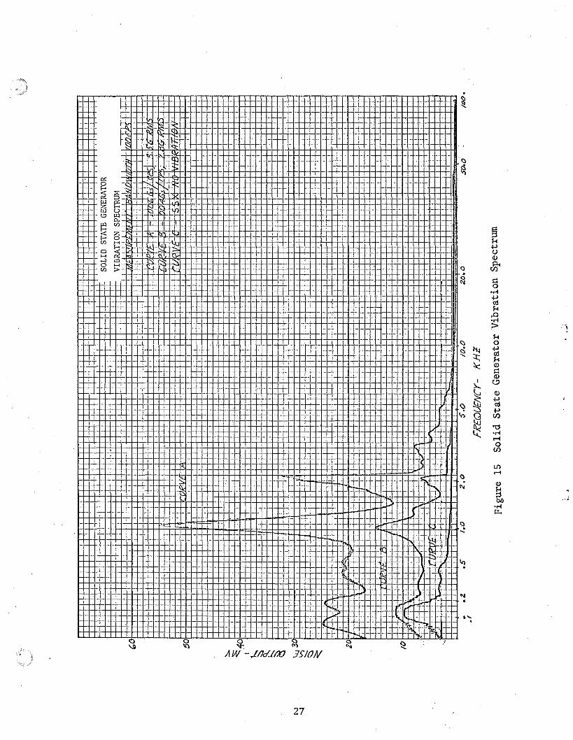
the spectrum shown i n Figure 15.
An oscil loscope was used t o
A tape recorder was connected t o t h e
The curves show the output noise for :
. Nonvibrating, Power Output +24 dBm, Figure 15, Curve C
2 . Vibrating at .004G /cps, Power Output +24 dBm, Figure 15, Curve B
2 . Vibrating a t .006G /cps, Power Output +24 dBm, Figure 15, Curve A
The dr ive s igna l was white noise with a 20 Hz t o 20 kHz bandwidth.
3.2.3 Results and Conclusions
The spec t ra l p lo t s (Figure 14) show t h a t there are s igna l outputs a t some
spec i f ied frequencies below 5 kHz.
This indicates t h a t some pa r t s o f
each spec i f i c frequency. Because
o f t he sandwiched s t r i p l i n e board
is caused by one o r a combination
the un i t are mechanically resonating at of t h e excel lent mechanical propert ies
assembly, it i s f e l t t h a t t h e noise
of the following:
25
* rl
26
27
a. Mechanical vibrat ion transmitted t o the Johannson capacitors.
b . Mechanical vibrat ion transmitted t o t h e walls o f t h e waveguide hybrid.
c. Mechanical vibrat ion transmitted t o the f l ex ib l e waveguide.
I t was not possible t o iden t i fy the noise peaks with the possible main
sources.
un i t s .
types o f waveguide.
However, t he first two causes can readi ly be eliminated i n later The l a s t source can be iden t i f i ed by use of various lengths and
Funding l i m i t s d id not allow fur ther invest igat ion.
3.3 TEMPERATURE TESTS
3.3.1 Test Procedure
The s o l i d s t a t e generator was placed i n an oven with a waveguide connecting
the output t o a c rys t a l diode detector . t he random noise bu r s t s .
An oscil loscope and a wave analyzer were connected t o the output o f the 80 dB amplif ier t o observe the noise output during the temperature run.
An oscil loscope was used t o monitor
In addition, frequency and a power were measured.
3.3.2 Results and Conclusions
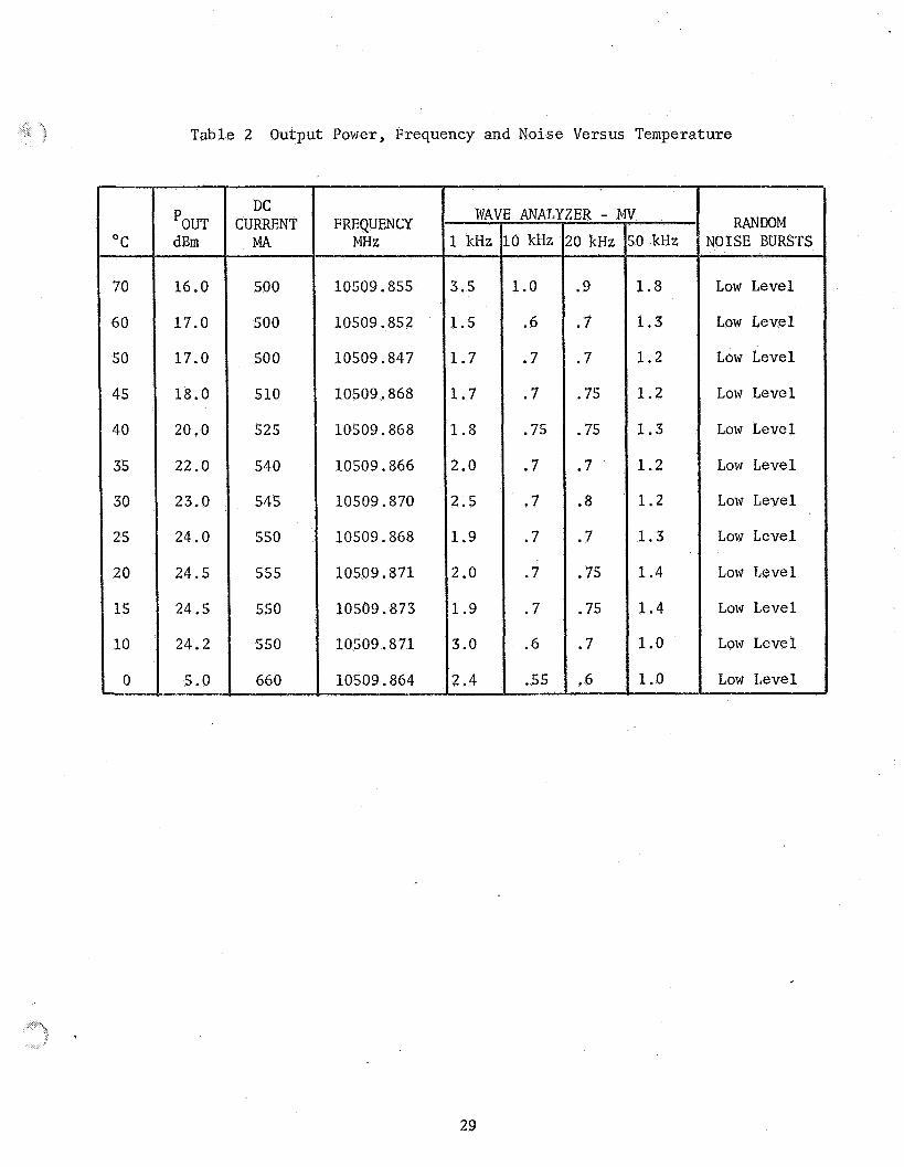
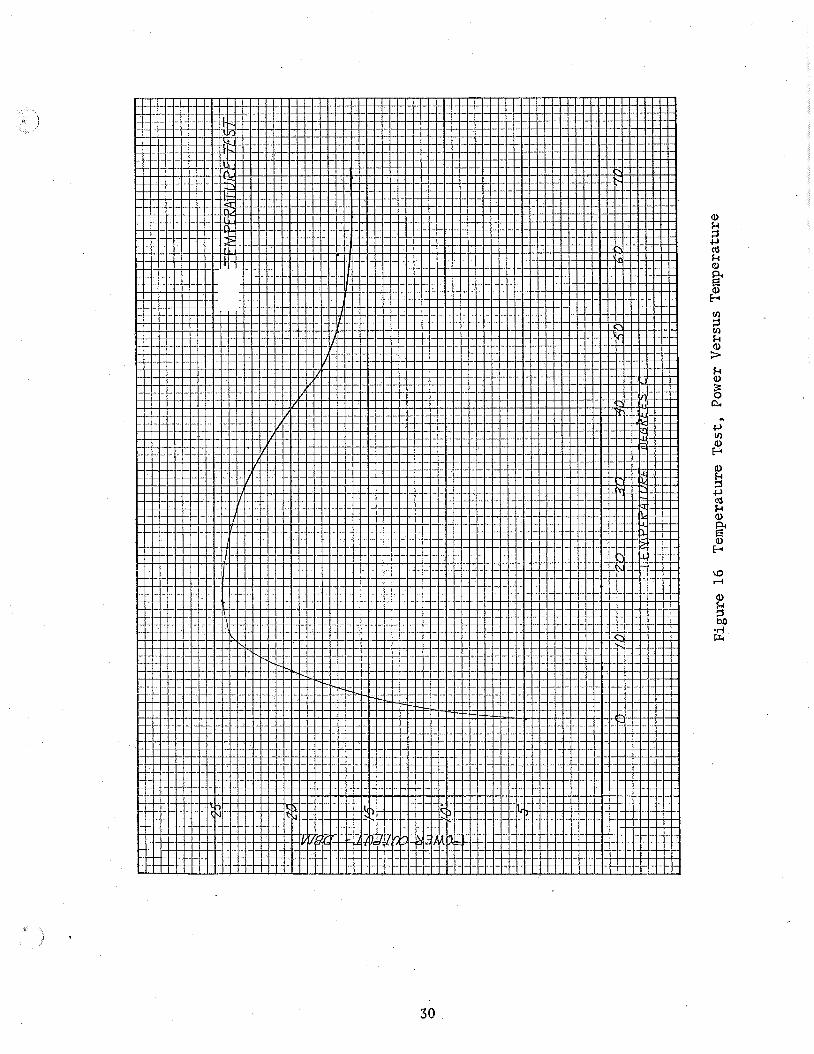
The r e s u l t s o f power output versus temperature are shown i n Figure 16, while
frequency var ia t ions and noise burs t s are linked i n Table 2.
indicates t h a t t he frequency s t a b i l i t y was excel lent and the random noise
burs t s and rms noise were low a t each spec i f ied s t a b i l i z e d temperature.
. This data
Further examination of Table 2 shows t h a t the +28 vdc input current changed
over the temperature range.
the impedance match i n t h e input and output c i r c u i t s o f t he L-band amplifier.
The changes i n the matching circuits resu l ted i n changes i n VSWR, which
were r e f l ec t ed back t o the t r a n s i s t o r co l l ec to r c i r c u i t causing changes
i n the output of the amplifier.
I t is f e l t t h a t t h i s i s caused by changes i n
28
O C
70
60
so 45
40
35
30
25
20
15
10
0
-
_._
Table 2 Output Power, Frequency and Noise Versus Temperature
'OUT dBm
16.0
17.0
17.0
18.0
20.0
22.0
23.0
24.0
24.5
24.5
24.2
5.0
DC CURRENT
MA
500
500
50 0
510
525
540
545
550
555
550
550
660
FREQUENCY MHz
10509.855
10509.852
10509.847
10509.868
10509.868
10509.866
10509.870
10509.868
10509.871
10509.873
10509.871
10509.864
WA'
1 kHz
3.5
1 .5
1 .7
1 .7
1 .8
2.0
2.5
1.9
2 .o
1.9
3.0
2.4
- ANAL'
D kHz
1.0
.6
.7
.7
.75
.7
. 7
.7
.7
.7
.6
.55
ER - I P
0 kHz
.9
.7
.7
.75
.75
.7
.8
.7
.75
.75
.7
.6
0 kHz
1.8
1 .3
1 . 2
1 . 2
1.3
1 . 2
1 . 2
1 .3
1.4
1.4
1 .o
1 .o
RANDOM NOISE BURSTS
Low Level
Low Level
Low Level
Low Level
Low Level
Low Level
Low Level
Low Level
Low Level
Low Level
Low Level
Low Level
29
a
30
The possible causes of the impedance change were:
Tuning Capacitors:
Temperature changes i n t h i s ro to r lock causes changes o f t he spring-finger
contacts which, i n tu rn , changes t h e c i r c u i t impedance match.
These capacitors are designed with a te f lon ro to r lock.
Di f fe ren t ia l Expansion:
between the aluminum heat s ink and the c i r c u i t boards caused small mechanical
changes i n the output c i r c u i t s of t h e s t r i p l i n e boards. The resu l t ing m i s - match was ref lec ted back t o the t r a n s i s t o r co l l ec to r c i r c u i t and, hence,
t he power output was modified.
The difference i n the coef f ic ien t of expansion
.
3 . 3 . 3 Effects o f a Rapid Change i n Temperature
The generator was s t a b i l i z e d at a temperature where t h e random noise burs t s
were low,
output observed . The temperature was changed 10°C i n one minute and the noise
3 . 3 . 4 Results and Conclusions
The random noise bu r s t s , as observed by monitoring t h e amplifier output of
an oscil loscope, increased t o a very high level .
again s t ab i l i zed , the random noise output decreased.
l i ke ly caused by d i f f e ren t i a l thermal expansions and can be cured by proper
When the temperature
This e f f e c t is most
se lec t ion of materials and elimination of the tuning caTacitor.
581T800 1 2
3
4 5
6
7
8
10
11
12
13
14
15
16
1 7
18
19
20
2 1
22
23
24
25
26
27
28
29
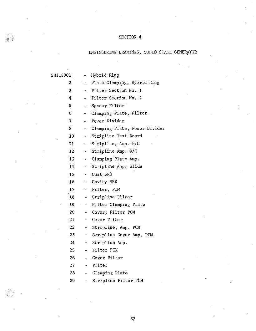
SECTION 4
ENGINEERING DRAWINGS, SOLID STATE GENERATOR
- Hybrid Ring
- Plate Clamping, Hybrid Ring
- F i l t e r Section No. 1 - F i l t e r Section No. 2
- Spacer F i l t e r
- Clamping Plate, F i l t e r
- Power Divider
- Clamping Plate, Power Divider
- S t r i p l i n e Test Board
- S t r i p l i n e , Amp. P/C
- S t r i p l i n e Amp. D/C
- Clamping Plate Amp. - S t r i p l i n e Amp. S l ide
- Dual SRD
- Cavity SRD
- Fi l t e r , PCM
- S t r i p l i n e F i l t e r
- F i l t e r Clamping Plate
- Cover; F i l te r PCM
- Cover F i l t e r
- S t r i p l i n e , Amp. PCM
- S t r i p l i n e Cover Amp. PCM
- S t r i p l i n e Amp. - Fil ter PCM
- Cover F i l t e r
- F i l t e r
- Clamping Plate
- S t r i p l i n e F i l t e r PCM
32
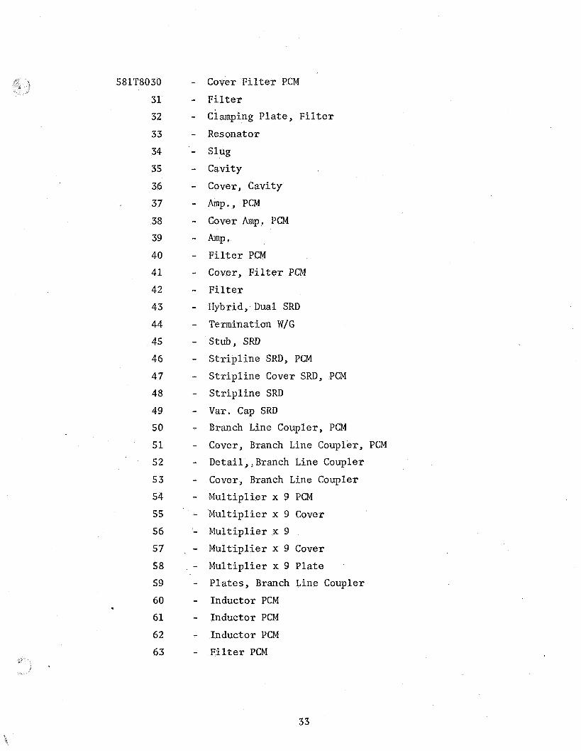
581T8030
31
32
33
34
35
36
37
38
39
40
41
42
43
44
45
46
47
48
49
50
51
52
53
54
55
56
57
58
59
60
61
62
63
dl
Cover F i l t e r PCM
F i l t e r Ciamping Plate, F i l t e r
Res onat o r
Slug
Cavity
Cover, Cavity
Amp., PCM
Cover Amp. PCM
AmP *
F i l t e r PCM
Cover, F i l t e r PCM F i l t e r
Hybrid, Dual SRD
Termination W/G Stub, SRD
S t r i p l i n e SRD, PCM
S t r i p l i n e Cover SRD, PCM
S t r i p l i n e SRD
Var. Cap SRD Branch Line Coupler, PCM
Cover, Branch Line Coupler, PCM
Detail , Branch Line Coupler
Cover, Branch Line Coupler
Mul t ip l ie r x 9 PCM
Mul t ip l ie r x 9 Cover
Mul t ip l ie r x 9
Mult ip l ie r x 9 Cover
Mul t ip l ie r x 9 Plate
Plates, Branch Line Coupler
Inductor PCM
Inductor PCM
Inductor PCM
F i l t e r PCM
33
.. i
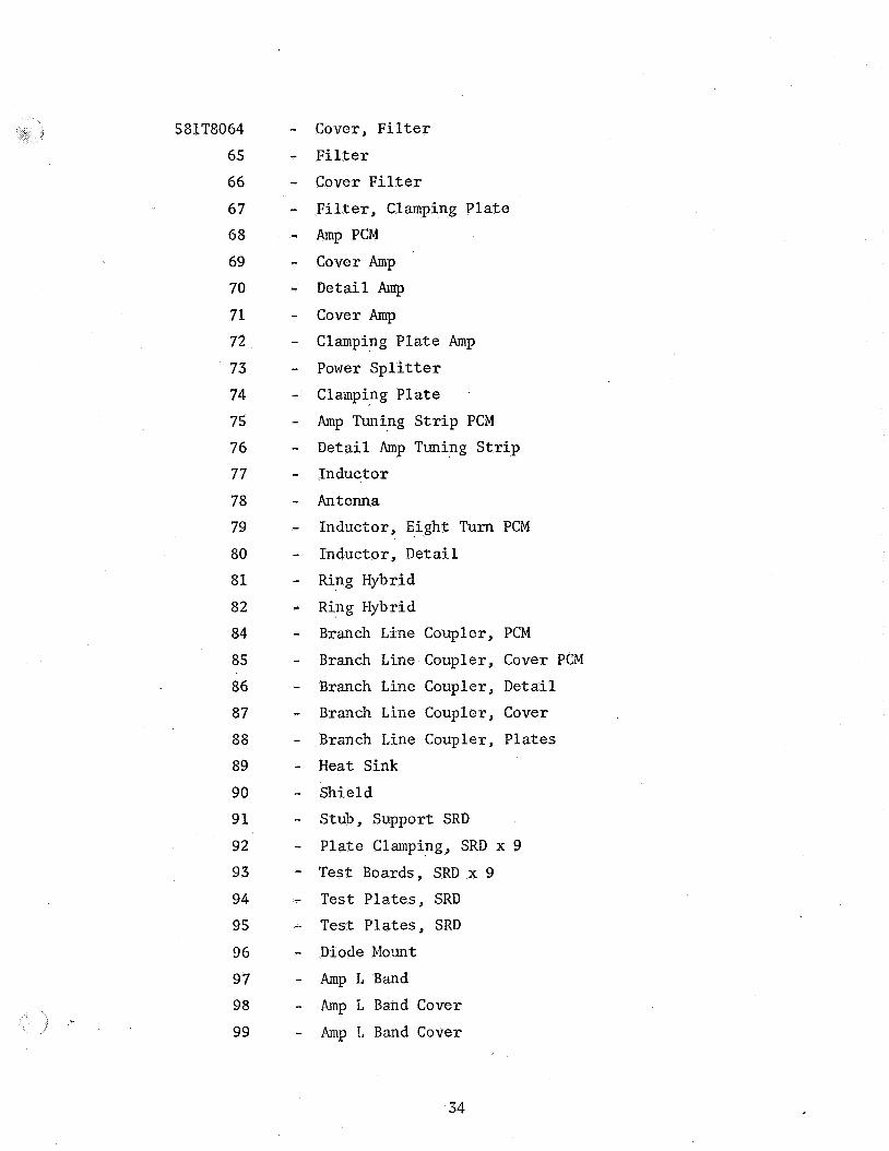
5 UT8064
65
66
67
68
69
70
71
72
73
74
75
76
77
78
79
80
8 1
82
84
85
86
87
88
89
90
9 1
92
93
94
95
96
97
98
99
Cover , F i l t e r
F i l t e r
Cover F i l t e r
F i l t e r , Clamping Plate
Amp PCM
Cover Amp
Detail Amp
Cover Amp Clamping Plate Amp
Power S p l i t t e r
Clamping Plate
Amp Tuning S t r i p PCM
Detail Amp Tuning S t r i p
Inductor
Antenna Inductor, Eight Turn PCM
Inductor, Detail
Ring Hybrid
Ring Hybrid
Branch Line Coupler, PCM
Branch Line Coupler, Cover PCM
Branch Line Coupler, Detail
Branch Line Coupler, Cover
Branch Line Coupler, Plates
Heat Sink
Shield
Stub, Support SRD
Plate Clamping, SRD x 9
Test Boards , SRD x 9
Test Plates , SRD
Test Plates, SRD
Diode Morrnt
Amp L Band
Amp 1, Band Cover
Amp I, Band Cover
34
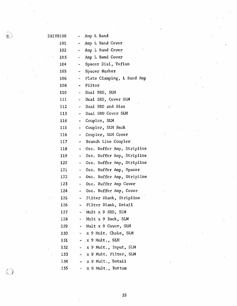
581T8100
101
102
103
104
105
106
108
110
111
112
113
114
115
116
117
118
119
120
1 2 1
122
123
124
125
126
127
128
129
130
131
132
133
1 34
135
Amp L Band
Amp L Band Cover
Amp L Band Cover
Amp L Band Cover
Spacer Dial, Teflon
Spacer Washer
Plate Clamping, L Band Amp F i l t e r
Dual SRD, SLM
Dual SRD, Cover SLM
Dual SRD and Bias Dual SRD Cover SLM
Coupler, SLM
Coupler, SLM Back
Coupler, SLM Cover
Branch Line Coupler
Osc. Buffer Amp, S t r i p l i n e
Osc. Buffer Amp, S t r i p l i n e
Osc. Buffer Amp, S t r i p l i n e
Osc. Buffer Amp, Spacer
Osc. Buffer Amp, S t r i p l i n e
Osc. Buffer Amp Cover
Osc. Buffer Amp, Cover
F i l t e r Blank, S t r i p l i n e
F i l t e r Blank, Detail
Mult x 9 SRD, SLM
Mult x 9 Back, SLM
Mult x 9 Cover, SLM
x 9 Mult. Choke, SLM
x 9 Mult . , SLM
x 9 Mult., Input, SLM
x 9 Mult. F i l t e r , SLM
x 9 Mult., Detail x 9 Mult . , Bottom
35
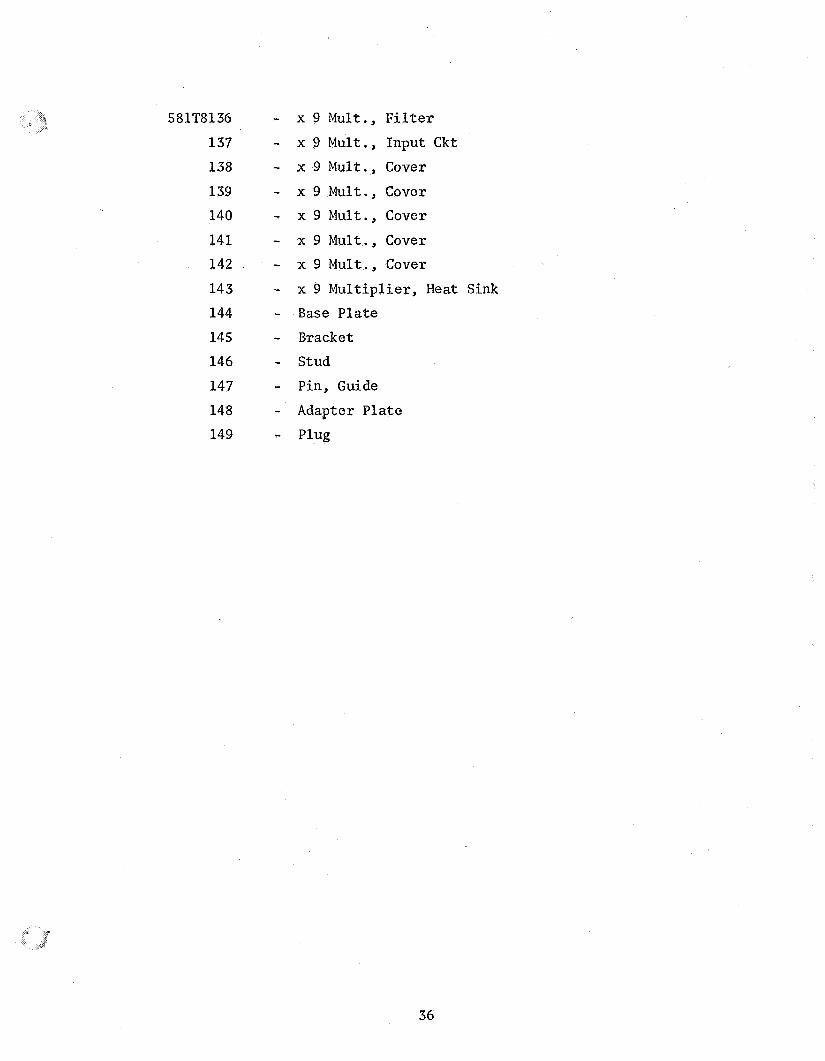
5 81T8136 -. 137 - 138 - 139 - 140 - 141 - 142 . - 14 3 - 144 - 145 - 146 - 147 - 148 - 149 -
x 9 Mult., F i l t e r
x 9 Mult., Input Ckt
x 9 Mult., Cover
x 9 Mult . , Cover
x 9 Mult., Cover
x 9 Mult., Cover
x 9 Mult., Cover
x 9 Mult ipl ier , Heat Sink
Base Plate
Bracket Stud
Pin, Guide
Adapter Plate
Plug
36