Embed Size (px)
Citation preview

APPLICATION NOTE
R01AN0902EU0201 Rev. 2.01 Page 1 of 29 Jul. 30, 2014
RX62T Three-Shunt Sensorless Vector Control of Permanent Magnet Synchronous Motors (PMSM) with Internal Programmable Gain Amplifier (PGA) Introduction This document presents the RX62T three-shunt sensorless vector control solution using the internal PGA, which has been implemented on the RX62T evaluation kit with three-shunt current measurements. It describes the evaluation kit hardware setup for the internal PGA, the RX62T PGA, the PGA related sample circuit design, the gain calculation, and software implementation. For the three-shunt sensorless vector control, please refer to the application note of “Three-Shunt Sensorless Vector Control of PMSM”.
Target Device RX62T
Contents
1. Overview ........................................................................................................................................... 2
2. Specification and Performance Data ................................................................................................ 3
3. Hardware Platform and Setup for PGA ............................................................................................. 4
4. RX62T PGA....................................................................................................................................... 7
5. PGA Related Sample Circuit Design and Gain Calculation .............................................................. 8
6. Software Implementation ................................................................................................................ 13
7. Demonstration Guide ...................................................................................................................... 16
Appendix A - References ........................................................................................................................ 28
R01AN0902EU0201 Rev. 2.01
Jul. 30, 2014

RX62T Three Shunt Sensorless Vector Control of PMSM with Internal Programmable Gain Amplifier (PGA)
R01AN0902EU0201 Rev. 2.01 Page 2 of 29 Jul. 30, 2014
1. Overview The sensorless vector control requires the current measurement for three-shunt or single-shunt. Traditionally, the current is sampled and amplified by an external amplifier before inputting it to the ADC channels of the microcontroller. It is not complex to design the linear amplifier circuit, but the extra circuits add to the hardware cost and increase the board size.
For the Renesas RX62T microcontroller, the PGA adds additional functionality, and it is integrated in the 12-bit ADC modules. 6 ADC channels for the AN000 to AN002 and AN100 to AN102 can be selected for amplification. The PGA gain value is programmable to 13.3/10.0/6.7/5.7/5.0/4.4/4.0/3.6/3.1/2.5/2.0/1.0. The outputs go into the analog multiplexer of the ADC converter, allowing the amplified signal to be converted by the ADC.
The PGA does not require feedback and input resistance, therefore, it can significantly reduce costs and save board space. Since the gains can be configured through software control, it makes the controls have high adaptability and flexibility. The PGA with the RX62T reduces the amount of components from the original design, and it can greatly simplify the previously complex circuit design and improve work efficiency.
The software described in this application note is applicable to the following devices and platforms:
MCU: RX62T and RX62N Motor: Three-Phase Brushless DC (BLDC) and PMSM Platform: Renesas Evaluation Kit Control algorithm: Three-Shunt Sensorless Vector Control Using Internal PGA

RX62T Three Shunt Sensorless Vector Control of PMSM with Internal Programmable Gain Amplifier (PGA)
R01AN0902EU0201 Rev. 2.01 Page 3 of 29 Jul. 30, 2014
2. Specifications and Performance Data The implementation of the three-shunt sensorless vector control solution using an internal PGA is based on the Renesas evaluation kit and the RX62T MCU. The main specifications are described as following:
Input Voltage: 24VDC Rated Bus Voltage: 24V Output Voltage: 24VAC Rated Output Power: 120W PWM Switch Frequency: 20KHz Control Loop Frequency: 10KHz Current Measurement: 3 Shunt Resistors Implementation: FPU CPU Bandwidth: 20% Used Flash Memory: 33.824Kbytes Used RAM: 4.397Kbytes Used Stack : 336bytes

RX62T Three Shunt Sensorless Vector Control of PMSM with Internal Programmable Gain Amplifier (PGA)
R01AN0902EU0201 Rev. 2.01 Page 4 of 29 Jul. 30, 2014
3. Hardware Platform and Setup for PGA The RX62T evaluation board is a single board with an integrated power inverter with the controller. The hardware includes a low-voltage MOSFET power stage, a communication stage, and a RX62T microcontroller based controller as shown in Figure 1.
The board has the following features:
A complete 3-phase inverter with a low-voltage motor 24V external power supply to provide DC bus voltage, 15V and 5V power supply Power devices use Renesas low-voltage MOSFETs Power rating up to 120 watts Supports three-shunt and single-shunt current measurements Easily change jumpers from the external amplifiers to the internal PGA USB communication with the PC via a H8S2212 MCU Graphical User Interface (GUI) used to both modify the motor and control parameters and tune the speed and
position control Connectors for Hall sensors and encoder connections LCD to monitor the operation status Supports the standalone mode set by potentiometer and push-buttons Supports the second motor drive, signals, and connector for another motor control power stage
Figure 1 Evaluation Board

RX62T Three Shunt Sensorless Vector Control of PMSM with Internal Programmable Gain Amplifier (PGA)
R01AN0902EU0201 Rev. 2.01 Page 5 of 29 Jul. 30, 2014
Figure 2 shows the evaluation kit hardware circuit for the three-shunt current measurements. Jumpers J6 and J9 are shorted, while J7 and J8 are open. The composite currents of all three MOSFET inverter low side legs can be measured with a single shunt resistor of 0.1Ω, or that the current in each individual leg can be determined with three shunt resistors. Table 1 lists the jumper setting for the three-shunt current measurements.
Figure 2 Three-Shunt Current Measurements in the Low Side Inverter Legs
Table 1 Jumper Settings for Three-Shunt Current Measurements
Jumper J6 J7 J8 J9
State ON OFF OFF ON

RX62T Three Shunt Sensorless Vector Control of PMSM with Internal Programmable Gain Amplifier (PGA)
R01AN0902EU0201 Rev. 2.01 Page 6 of 29 Jul. 30, 2014
The motor currents of wvu iii ,, are measured by three shunt resistors. The shunt currents ( wvu iii ,, ) are measured by a 12-bit ADC unit 0 of channel AN002, AN001and AN000. All three ADC channels have PGA support. Figure 3 shows the three-shunt current sample amplifier circuit with the 2.5V DC offset. If using the internal PGA, the external amplifiers in the red frame can be removed. The jumpers of JP10, JP11 and JP12 are set to 2-3. The outputs from the three shunt resistors directly input to the microcontroller after the 5V limit and the small capacitor filter. Table 2 lists the jumper settings for the internal PGA selection.
Figure 3 Three-Shunt Current Sampling with External Amplifier
Table 2 Jumper Settings for Internal PGA
Jumper JP10 JP11 JP12 JP13 JP14 JP15
Pins 2-3 2-3 2-3 3-4 3-4 3-4

RX62T Three Shunt Sensorless Vector Control of PMSM with Internal Programmable Gain Amplifier (PGA)
R01AN0902EU0201 Rev. 2.01 Page 7 of 29 Jul. 30, 2014
4. RX62T PGA RX62T 12-bit ADC converters include a PGA for additional functionality. The two units of ADC: unit0 (S12ADA0) and unit1 (S12ADA1), can be operated separately. PGA and comparators are provided for AN000 to AN002 and AN100 to AN102. Figure 4 shows the structure of the ADC converter unit0 3 channels with the PGA. It can be seen that each of the ADC channels (AN000, AN001, and AN002) have a separate PGA. It is the same configuration for the ADC unit1. Each PGA should be enabled and defined to be used by the ADC channel selection register. The default is to by-pass the internal PGA.
All three channels have separate sample and hold circuits, which allows the three-shunt currents to be simultaneously sampled.
Figure 4 Structure of the RX62T ADC unit0 AN000, AN001, AN002 with PGA The amplification rate includes 2.0, 2.5, 3.077, 3.636, 4.0, 4.444, 5.0, 5.714, 6.667, 10.0, or 13.333 times amplification, a total of 11 steps as listed in Table 3. The gain can be selected through the ADPG.PGnGAIN[3:0] bits (n = 000 to 002 or 100 to 102), and the operational amplifier can be selected through the ADANS.PGnEN and ADANS.PGnSEL bits.
Table 3 PGA Gain Steps
Amp Gain
x 2.000 x 4.444 x 13.333
x 2.500 x 5.000
x 3.077 x 5.714
x 3.636 x 6.667
x 4.000 x 10.000

RX62T Three Shunt Sensorless Vector Control of PMSM with Internal Programmable Gain Amplifier (PGA)
R01AN0902EU0201 Rev. 2.01 Page 8 of 29 Jul. 30, 2014
Table 4 shows characteristics of the PGA. The items for which test conditions are not specifically stated in the table below have the same values under conditions 1 to 3.
Condition 1: VCC = PLLVCC = 2.7 to 3.6 V, VSS = PLLVSS = AVSS0 = AVSS = VREFL0 = 0 V AVCC0 = AVCC = 3.0 to 3.6 V, VREFH0 = 3.0 V to AVCC0, VREF = 3.0 V to AVCC
Condition 2: VCC = PLLVCC = 2.7 to 3.6 V, VSS = PLLVSS = AVSS0 = AVSS = VREFL0 = 0 V AVCC0 = AVCC = 4.0 to 5.5 V, VREFH0 = 4.0 V to AVCC0, VREF = 4.0 V to AVCC
Condition 3: VCC = PLLVCC = 4.0 to 5.5 V, VSS = PLLVSS = AVSS0 = AVSS = VREFL0 = 0 V AVCC0 = AVCC = 4.0 to 5.5V, VREFH0 = 4.0 V to AVCC0, VREF = 4.0 V to AVCC
Ta = −40 to +85°C. Ta is the same under conditions 1 to 3.
Table 4: Characteristics of the PGA
5. PGA Related Sample Circuit Design and Gain Calculation 5.1 Difference Between External Amplifier and PGA Figure 5 just shows one of the shunt current sample and external amplifier circuits. Because of the current polarity, the offset should be added to shift the maximum negative current to 0 volts. R1and Rs have been set in order to get Vin = 2.5V at Is = 0. The output of the amplifier is:

RX62T Three Shunt Sensorless Vector Control of PMSM with Internal Programmable Gain Amplifier (PGA)
R01AN0902EU0201 Rev. 2.01 Page 9 of 29 Jul. 30, 2014
Vout = gain × Vin + Voffset
Set Rd and Re for the amplifier gain to make Vout = 5V or less.
Figure 5 Motor Current Measurement with External Amplifier
Figure 6 depicts one of the shunt current samples with the internal PGA. Actually, there is no amplifier circuit required, because it is integrated with the RX62T microcontroller 12-bit ADC. The outside circuit only needs two resistors.
Because of the current polarity, the offset should be added to shift the maximum negative current above 0 volts. R1, R2, and Rs have been set in order to get:
Vin = 0V + x
x is a small, positive value above 0.1 volts to less than 2 volts, which depends on the PGA gain.
Define the PGA register for the gain to get Vout = 5V or less:
Vout = gain × Vin
Figure 7 clearly shows the difference between these two amplifiers. The external amplifier shifts the output voltage from the shunt resistor to the positive value. The offset makes 0 to 2.5V. When the gain equals 2.5:
Vout_max = 2.5 + 1 × 2.5 = 5V
Vout_min = 2.5 − 1 × 2.5 = 0V
The input voltage to the ADC channels is 0 to 5 volts.
On the other hand, for the internal PGA, there is no offset circuit for the internal amplifier. It just amplifies the voltage to the maximum 5 volts. Therefore, the input voltage to the ADC should be a small positive value for the maximum polarity current. As described above, R1 and R2 can be set to make the input voltage as:
Vin = 0V + x
For example, in Figure 7, x equals 0.235 to 1.5V. If the PGA gain is set as 2.5, the ADC sample voltage would be 0.5875V for the maximum -5 Amps current, and 3.75V for the maximum 5 Amps current for the evaluation board.

RX62T Three Shunt Sensorless Vector Control of PMSM with Internal Programmable Gain Amplifier (PGA)
R01AN0902EU0201 Rev. 2.01 Page 10 of 29 Jul. 30, 2014
Figure 6 Motor Current Measurement with PGA
Figure 7 Motor Current Sensing Comparison Between External Amplifier and PGA
5.2 PGA Gain Calculation Figure 8 shows the shunt current measurement with the PGA. The shunt resistor used in this application is 0.1Ω. The measured current range is from -5A to 5A. The voltage of the shunt resistance is from -0.5V to 0.5V. R1 and R2 resistors are selected to make this voltage to the some positive value.
The value of Vs, Vin and Vout can be estimated as below:
Vs[V] = 0[V] ± Rs x Is

RX62T Three Shunt Sensorless Vector Control of PMSM with Internal Programmable Gain Amplifier (PGA)
R01AN0902EU0201 Rev. 2.01 Page 11 of 29 Jul. 30, 2014
Vin[V] = Vref × R1R1 + R2
± Rs × Is × R2
R1 + R2
Vout[V] = G × Vref × R1
R1 + R2 ±
G × Rs × Is × R2R1 + R2
Vout includes two parts: one is for the offset part voltage and the other is for the gain voltage.
The offset voltage and gain voltage of the RX62T are under:
G × Vref × R1R1 + R2
= 2.5
G × Rs × Is × R2R1 + R2
≦ 2.5
Circuit condition is with Vref = 5V, Is = 5A, R2 = kR1
5 × G × R1R1 + kR1
= 2.5,
Rs × 5G × kR1R1 + kR1
≦ 2.5
Therefore,
2G = 1 + k
2 x kG x Rs ≦ 1 + k
Gain k = 4 and Rs = 0.1Ω set to the equations above:
R1 = 1KΩ
R2 = 6.8kΩ
They are selected by the evaluation kit. Therefore the voltages are:
iu = 0A, the voltage to the ADC of Vu = 0.6V
iu = -5A, Vu = 0.16V
iu = 5A, Vu = 1.04V.
And the internal amplifier gain is set as 4.

RX62T Three Shunt Sensorless Vector Control of PMSM with Internal Programmable Gain Amplifier (PGA)
R01AN0902EU0201 Rev. 2.01 Page 12 of 29 Jul. 30, 2014
Figure 8 Shunt Current Sensing with PGA

RX62T Three Shunt Sensorless Vector Control of PMSM with Internal Programmable Gain Amplifier (PGA)
R01AN0902EU0201 Rev. 2.01 Page 13 of 29 Jul. 30, 2014
6. Software Implementation The three-shunt sensorless vector control software is the same as the one in the Application Note of “Three-Shunt Sensorless Vector Control of PMSM”. This section just explains how to set up the registers and modify the gain for the internal PGA in the software.
If the internal PGA is used, the changes of the software are only for the ADC registers and the gain of the three-shunt current measurement. Two ADC registers should be defined for the PGA usage.
6.1 ADC Channel Select Register (ADANS) Figure 9 defines the bit definition of the ADC channel select register for three-shunt current measurements. If the bits 0 to 2 are set to 1, the PGAs for AN000, AN001, and AN002 are enabled. These channels are used to sample the three-shunt currents. The bits 8 to 10 need to set to 1 in order to select AN000, AN001 and AN002 PGAs. Therefore, this register is set as 0707 for this application.
Figure 9 Bit Definition of the ADC Channel Select Register for Three-Shunt Current Measurements
6.2 ADC Programmable Gain Amplifier Register (ADPG) Figure 10 defines the bit definition of the ADC PGA register for the three-shunt current measurements. It defines the gain of the PGA for each ADC channel. The bits 0 to 3 are set for AN000; the bits 4 to 7 for AN001, and the bits 8 to 11 for AN002. Typically, the same gain is used for three-shunt currents. As calculated above in section 5.2 “PGA Gain Calculation”, the gain is set as 4 for this application. Therefore, the bits need to set as 0111 for each channel.

RX62T Three Shunt Sensorless Vector Control of PMSM with Internal Programmable Gain Amplifier (PGA)
R01AN0902EU0201 Rev. 2.01 Page 14 of 29 Jul. 30, 2014
Figure 10 Bit Definition of the ADC PGA Register for the Three-Shunt Current Measurements

RX62T Three Shunt Sensorless Vector Control of PMSM with Internal Programmable Gain Amplifier (PGA)
R01AN0902EU0201 Rev. 2.01 Page 15 of 29 Jul. 30, 2014
6.3 Current Gain Setting The shunt resistor 0.1Ω senses the maximum ±5Amps of current to convert the current to the ±0.5 voltage. R1 and R2 are 1KΩ and 6.8KΩ, respectively. When the shunt current iu = 0A, the voltage to the ADC of Vu = 0.6V; iu = -5A, Vu = 0.16V; iu = 5A, Vu = 1.04V. The internal amplifier gain is 4. The three-phase motor currents are measured as:
)002(* _ offsetuu iANKADIi −=
)001(* _ offsetvv iANKADIi −=
)000(* _ offsetww iANKADIi −=
)**4096/(5 KampRshuntKADI =
Where,
ui , vi ,and wi are three-phase motor currents;
offsetui _ , offsetvi _ , and offsetwi _ are u , v and w phase current offsets, respectively;
002AN , 001AN , and 000AN are the 12-bit ADC reading values of u , v and w phase shunt currents;
KADI is the motor phase current scaling;
Rshunt is the value of the shunt resistor;
Kamp is the gain of the internal PGA.

RX62T Three Shunt Sensorless Vector Control of PMSM with Internal Programmable Gain Amplifier (PGA)
R01AN0902EU0201 Rev. 2.01 Page 16 of 29 Jul. 30, 2014
7. Demonstration Guide 7.1 Introduction to the Demonstration Guide The purpose of this Demonstration Guide is to help users get up and running quickly with the RX62T motor control kit (YMCRPRX62T). The RX62T Microcontroller is pre-programmed to run “Three-Shunt Sensorless Vector Control with External Amplifier”. Therefore, the user will need to reprogram the board using the E1 programmer/debugger to demonstrate the Three-Shunt Sensorless Vector Control of PMSM with Internal PGA, and later sections will explain how to (1) setup the demo board, (2) build and debug the demo project with e2studio, and (3) run the GUI application. The user needs to connect the motor and the power supply to experience the efficient motor control capabilities of the Renesas RX62T microcontroller.
Caution: Do not connect power to the board until all instructions are followed. The Demo contains the following items:
• RX62T Motor Control Evaluation Board (YMCRPRX62T) • One BLDC Motors with a 3-way Molex connector and encoder cable • 24V DC power supply • E1 debugger • Mini-USB cable • CD ROM for motor firmware and application GUI
7.2 Demo Board Setup Figure 11 (a) shows the board with the motor connected to J8 and the power supply to J3. There are four push‐buttons, a thumb‐wheel potentiometer, a graphic LCD, and a few simple steps to quickly operate the motor out of the box. For debugging or programming, the user needs to connect J5 with E1. Use the Mini-USB connector, J1, in the evaluation board for communication to the GUI.
(a) Board Layout (b) Functional Layout
Figure 11 Board Layout Before starting the demo, reconfigure the jumpers (JP6 – JP15) as highlighted with red in Table 5. The jumper’s location is shown in Figure 11 (b). The board can be operated in standalone mode or in GUI mode.
Table 5 Configuration Jumper Settings
Operation JP6 JP7 JP8 JP9 JP10 JP11 JP12 JP13 JP14 JP15
External OPA 3 - Shunt 1 - 2 – – 1 - 2
1 - 2 1 - 2 1 - 2 1 - 2 1 - 2 1 - 2 1 - Shunt – 1 - 2 1 - 2 –
Internal PGA 3 - Shunt 1 - 2 – – 1 - 2
2 – 3 2 - 3 2 - 3 3 - 4 3 - 4 3 - 4 1 - Shunt – 1 - 2 1 - 2 –
RX62T Three Shunt Sensorless Vector Control of PMSM with Internal Programmable Gain Amplifier (PGA)
R01AN0902EU0201 Rev. 2.01 Page 17 of 29 Jul. 30, 2014
For standalone mode, press and hold P4 (mode) button during power cycle or P6 (reset). Then, release the P4 button. Now the board is in standalone mode. Press P1 (start/stop) to start or stop motor. Set RV1 for motor speed and change motor rotation direction by pressing P2 (forward) or P3 (reverse) button. P4 toggles different modes on the LCD.
Note: The user needs to set speed to 2000 rpm or more to run the motor in this demo. GUI mode will be explained in section 7.4.
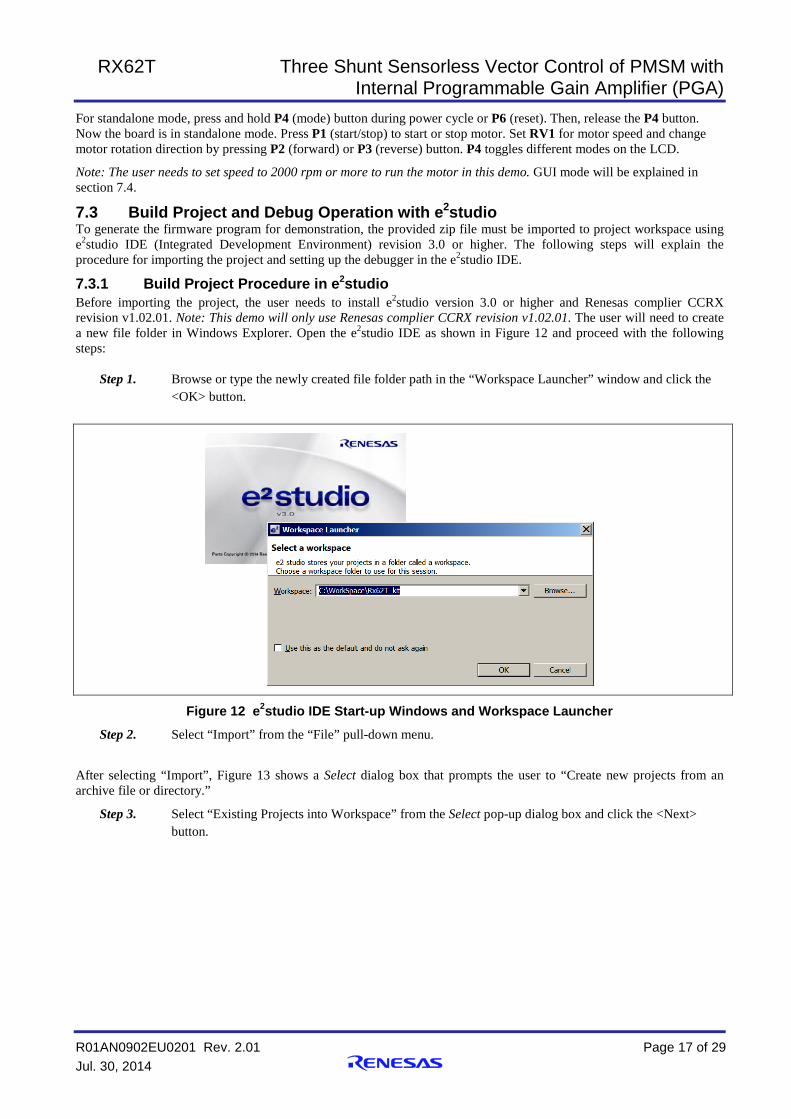
7.3 Build Project and Debug Operation with e2studio To generate the firmware program for demonstration, the provided zip file must be imported to project workspace using e2studio IDE (Integrated Development Environment) revision 3.0 or higher. The following steps will explain the procedure for importing the project and setting up the debugger in the e2studio IDE.
7.3.1 Build Project Procedure in e2studio Before importing the project, the user needs to install e2studio version 3.0 or higher and Renesas complier CCRX revision v1.02.01. Note: This demo will only use Renesas complier CCRX revision v1.02.01. The user will need to create a new file folder in Windows Explorer. Open the e2studio IDE as shown in Figure 12 and proceed with the following steps:
Step 1. Browse or type the newly created file folder path in the “Workspace Launcher” window and click the <OK> button.
Figure 12 e2studio IDE Start-up Windows and Workspace Launcher
Step 2. Select “Import” from the “File” pull-down menu.
After selecting “Import”, Figure 13 shows a Select dialog box that prompts the user to “Create new projects from an archive file or directory.”
Step 3. Select “Existing Projects into Workspace” from the Select pop-up dialog box and click the <Next> button.

RX62T Three Shunt Sensorless Vector Control of PMSM with Internal Programmable Gain Amplifier (PGA)
R01AN0902EU0201 Rev. 2.01 Page 18 of 29 Jul. 30, 2014
Figure 13 Importing Projects into the Workspace 1 of 2
After clicking the <Next> Button, the Import Projects dialog box in Figure 14 prompts the user to “Select a directory to search for existing Eclipse projects.”
Step 4. Select the Radio Button “Select archive file” and click <Browse> to locate the Three-Shunt Sensorless Vector Control with Internal PGA zip file to import into the workspace.
The selected project will then appear with a checked box in the Projects message box as seen in Figure 14.
Step 5. Check the “Add project to working sets” check box, and then click the <Finish> button to complete the project import.

RX62T Three Shunt Sensorless Vector Control of PMSM with Internal Programmable Gain Amplifier (PGA)
R01AN0902EU0201 Rev. 2.01 Page 19 of 29 Jul. 30, 2014
Figure 14 Importing Projects into the Workspace 2 of 2 If the file does not appear with a check box in the Projects message box, the selected zip file is the wrong zip file type, or it was not properly exported. If the file already exists in the workspace, then the user will see a message that states, “Some projects cannot be imported because they already exist in the workspace.”
After clicking <Finish>, the imported project is now in the e2studio workspace shown in Figure 15, and the project should be in Debug mode by default.
Figure 15 Setting the Toolchain Version in the e2studio Workspace
Step 6. Select “Properties” from the “Project” pull-down menu and expand “C/C++ Build” section. Select the “Change Toolchain Version” option and set the “Available Versions” to v1.02.01.

RX62T Three Shunt Sensorless Vector Control of PMSM with Internal Programmable Gain Amplifier (PGA)
R01AN0902EU0201 Rev. 2.01 Page 20 of 29 Jul. 30, 2014
Step 7. Select the “Clean” command from the “Project” pull-down menu for cleaning and rebuilding the project.
Figure 16 shows the “Clean” Windows dialog box.
Step 8. Check the “Start a build immediately” option and select the Radio buttons “Clean all projects” and “Build the entire workspace.” Then click the <OK> button to clean and rebuild all projects in the workspace.
For debugging, the target firmware (.x file) is generated in the “Binaries” workspace folder shown in Figure 17. For release, set the active project to release mode for building projects. The target firmware (.mot file) is generated in the workspace “Release” folder.
Figure 16 Clean Message Box
Figure 17 Target Firmware in Workspace
RX62T Three Shunt Sensorless Vector Control of PMSM with Internal Programmable Gain Amplifier (PGA)
R01AN0902EU0201 Rev. 2.01 Page 21 of 29 Jul. 30, 2014
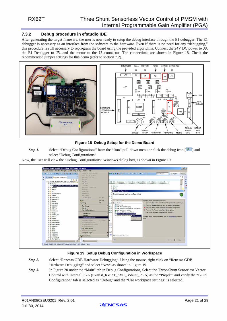
7.3.2 Debug procedure in e2studio IDE After generating the target firmware, the user is now ready to setup the debug interface through the E1 debugger. The E1 debugger is necessary as an interface from the software to the hardware. Even if there is no need for any “debugging,” this procedure is still necessary to reprogram the board using the provided algorithms. Connect the 24V DC power to J3, the E1 Debugger to J5, and the motor to the J8 connector. The connections are shown in Figure 18. Check the recommended jumper settings for this demo (refer to section 7.2).
Figure 18 Debug Setup for the Demo Board
Step 1. Select “Debug Configurations” from the “Run” pull-down menu or click the debug icon [ ] and select “Debug Configurations”
Now, the user will view the “Debug Configurations” Windows dialog box, as shown in Figure 19.
Figure 19 Setup Debug Configuration in Workspace
Step 2. Select “Renesas GDB Hardware Debugging”. Using the mouse, right click on “Renesas GDB Hardware Debugging” and select “New” as shown in Figure 19.
Step 3. In Figure 20 under the “Main” tab in Debug Configurations, Select the Three-Shunt Sensorless Vector Control with Internal PGA (EvaKit_Rx62T_SVC_3Shunt_PGA) as the “Project” and verify the “Build Configuration” tab is selected as “Debug” and the “Use workspace settings” is selected.

RX62T Three Shunt Sensorless Vector Control of PMSM with Internal Programmable Gain Amplifier (PGA)
R01AN0902EU0201 Rev. 2.01 Page 22 of 29 Jul. 30, 2014
Figure 20 Debug Configuration Main Dialog Box
Step 4. Select the “Debugger” tab as shown in Figure 21. Step 5. Select the “GDB Settings” sub-tab under the “Debugger” tab and set the “Debugger hardware” to “E1”
and “Target Device” to “R5F562TA”.
Figure 21 Debug Configuration Debugger Dialog Box
Step 6. Select the “Connection Settings” sub-tab and change the “External Frequency” value to 12.00 MHz and “JTag Clock Frequency” to 12.38 MHz. Set “Power” to “No.”
Step 7. Select the “Debug Tool Settings” sub-tab under the “Debugger” tab and select “Big Endian” in the “Endian” setting under “Memory.” Then click the <Apply> button.
The typical debug settings for this demo are shown with RED boxes in Figure 22 and in Figure 23.

RX62T Three Shunt Sensorless Vector Control of PMSM with Internal Programmable Gain Amplifier (PGA)
R01AN0902EU0201 Rev. 2.01 Page 23 of 29 Jul. 30, 2014
Figure 22 Debug Configuration Dialog Box 1 of 2
Figure 23 Debug Configuration Dialog Box 2 of 2
Step 8. Check the target board power is ON and verify the connections through the PC, E1 debugger, and the target board.
Clicking the <Debug> button in the “Debug Configurations” dialog box will download the firmware to the target board.
Step 9. Click the “Resume” icon [ ] or press the F8 Key to run the program. This may require the user to press the “Resume” icon or F8 multiple times depending on the delay in the code. The icon should turn gray when the program is running.
The LED DL1 will blink at about a one second rate continuously while running the target board.

RX62T Three Shunt Sensorless Vector Control of PMSM with Internal Programmable Gain Amplifier (PGA)
R01AN0902EU0201 Rev. 2.01 Page 24 of 29 Jul. 30, 2014
7.4 GUI Operation This operation requires the demo board to be connected to the PC using the supplied Mini-USB cable.
Step 1. Connect the Mini-USB cable to J1 from the PC LED DL8 is on when the USB bus power is applied to evaluation board. The PC will recognize the new hardware and will launch the driver installation screen. Follow the instruction from the “Message Box” to install respective USB device driver.
Note: Separate instructions for the USB device driver installation are provided in the Quick Start Guide or the driver will install automatically depending on the CD ROM installer. Figure 24 shows the necessary connections and LED designations.
Figure 24 Running the Demo with e2studio and the GUI
Step 2. Start the GUI program by double clicking on the Motor Control Demo icon [ ] or select the “Motor Control Demo” program from the Windows taskbar “Start” in “All Programs” under the “Motor Control Demonstrator” folder.
The GUI program screen will launch and display as shown in Figure 25. For a serial port update, wait for a few seconds to get the “Connect” button highlighted and then proceed to Step 3.
Note: If the “Connect” button is not highlighted, the GUI couldn’t find the correct USB device driver for COM port setting.
Step 3. Click the “Communication Settings” tab on the top left of the GUI seen in Figure 25 and select “Auto
detect” under the serial port drop-down tab.
Step 4. Click <Connect>.

RX62T Three Shunt Sensorless Vector Control of PMSM with Internal Programmable Gain Amplifier (PGA)
R01AN0902EU0201 Rev. 2.01 Page 25 of 29 Jul. 30, 2014
Figure 25 Connecting to the Motor Control Demo GUI 1 of 2
After successfully connecting with the target board, the “Communication Settings” area will change to a green color and the “Connect” button will change to “Disconnect.” The LED DL6 will blink while communicating between the target board and GUI.
Figure 26 shows the GUI after a successful connection.
Figure 26 Connecting to the Motor Control Demo GUI 2 of 2
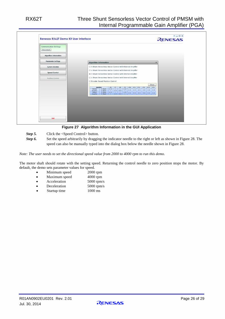
The GUI will detect the programmed algorithm. In this case the “3 Shunt Sensorless Vector Control with Internal Amplifier” will be used. After connection, the “Speed Control” button is active while the “Position Control” button is grayed out. The user can check with the “Algorithm Information” message box which shows a valid algorithm. Clicking the “Verify Jumper Settings” button shows Table 5 in the GUI. Figure 27 shows the “Algorithm Information” dialog box. Follow the below procedure for using the GUI. The LED DL1 will be blinking continuously while running demo with no fault occurrence. If a fault occurs, the LED DL2 will flash and DL1 will remain illuminated without flashing. If a fault occurs, press P6 (reset) and check if DL1 begins to blink. If pressing P6 does not fix the fault, disconnect and reconnect the E1 debugger and the Mini-USB and reprogram the board using the steps discussed in section 7.3.2.
RX62T Three Shunt Sensorless Vector Control of PMSM with Internal Programmable Gain Amplifier (PGA)
R01AN0902EU0201 Rev. 2.01 Page 26 of 29 Jul. 30, 2014
Figure 27 Algorithm Information in the GUI Application
Step 5. Click the <Speed Control> button. Step 6. Set the speed arbitrarily by dragging the indicator needle to the right or left as shown in Figure 28. The
speed can also be manually typed into the dialog box below the needle shown in Figure 28. Note: The user needs to set the directional speed value from 2000 to 4000 rpm to run this demo. The motor shaft should rotate with the setting speed. Returning the control needle to zero position stops the motor. By default, the demo sets parameter values for speed.
• Minimum speed 2000 rpm • Maximum speed 4000 rpm • Acceleration 5000 rpm/s • Deceleration 5000 rpm/s • Startup time 1000 ms

RX62T Three Shunt Sensorless Vector Control of PMSM with Internal Programmable Gain Amplifier (PGA)
R01AN0902EU0201 Rev. 2.01 Page 27 of 29 Jul. 30, 2014
Figure 28 Setting the Speed to Turn the Motor in the GUI Application
Step 7. Click the “Parameter Settings” button The “Parameter Settings” feature can be used to manually adjust the preset variables using the GUI. Figure 29 shows the “Parameter Settings” dialog box.
Figure 29 Changing the Parameter Settings in the GUI Application
If standalone mode is used the target board will “Disconnect” and no longer be communicating with the GUI. The LED DL6 will be on, but it will no longer be blinking. In order to reconnect from standalone mode, press P6 (reset) and “Connect” to the GUI using the User Interface.
To terminate the GUI application, return the control needle to zero position, press the “Disconnect” button and then press the “Exit” button to close the application.

RX62T Three Shunt Sensorless Vector Control of PMSM with Internal Programmable Gain Amplifier (PGA)
R01AN0902EU0201 Rev. 2.01 Page 28 of 29 Jul. 30, 2014
Appendix A - References 1. RX62T Group User’s Manual: Hardware, R01UH0034EJ0110, April 20, 2011
2. DevCon 2010 Courses:
ID-620C, Complete Motor Control Integration with RX62T.
ID-623C, Understanding Sensorless Vector Control with Floating Point Unit (FPU) Implementation.
3. Application Note of Sensorless Vector Control of Three-Phase PMSM Motors, REU05B0103-0100/Rev.1.00, March, 2009
4. Application Note of Mcrp05: Brushless AC Motor Reference Platform, REU05B0051-0100, Feb, 2009
5. Huangsheng Xu, Rohan Hubin, and Dave Cocca, “Sensorless Vector Control of PMSM Motor Using One Shunt Current Detection”, IEEE-IAS 2008, Oct. 5-9, Edmonton, Alberta, Canada.
6. Huangsheng Xu, and Yashvant Jani, “Understanding Sensorless Vector Control for Brushless DC Motors”, ESC-2008, Embedded System Silicon Valley Conference, April 15-17, San Jose, California, USA.

RX62T Three Shunt Sensorless Vector Control of PMSM with Internal Programmable Gain Amplifier (PGA)
R01AN0902EU0201 Rev. 2.01 Page 29 of 29 Jul. 30, 2014
Website and Support Renesas Electronics Website
http://www.renesas.com/ Inquiries
http://www.renesas.com/inquiry
All trademarks and registered trademarks are the property of their respective owners.


A-1
Revision Record Rev.
Date
Description Page Summary
1.00 Nov. 18, 2011. — First edition issued 2.00 Jan. 31, 2014. — Second edition issued 2.01 Jul. 30, 2014. 16 Demonstration Guide added

General Precautions in the Handling of MPU/MCU Products The following usage notes are applicable to all MPU/MCU products from Renesas. For detailed usage notes on the products covered by this manual, refer to the relevant sections of the manual. If the descriptions under General Precautions in the “Handling of MPU/MCU Products” and the body of the manual differ from each other, the description in the body of the manual takes precedence.
1. Handling of Unused Pins Handle unused pins in accord with the directions given under Handling of Unused Pins in the manual. The input pins of CMOS products are generally in the high-impedance state. In operation with an
unused pin in the open-circuit state, extra electromagnetic noise is induced in the vicinity of LSI, an associated shoot-through current flows internally, and malfunctions occur due to the false recognition of the pin state as an input signal become possible. Unused pins should be handled as described under Handling of Unused Pins in the manual.
2. Processing at Power-on The state of the product is undefined at the moment when power is supplied. The states of internal circuits in the LSI are indeterminate and the states of register settings and
pins are undefined at the moment when power is supplied. In a finished product where the reset signal is applied to the external reset pin, the states of pins are not guaranteed from the moment when power is supplied until the reset process is completed. In a similar way, the states of pins in a product that is reset by an on-chip power-on reset function are not guaranteed from the moment when power is supplied until the power reaches the level at which resetting has been specified.
3. Prohibition of Access to Reserved Addresses Access to reserved addresses is prohibited. The reserved addresses are provided for the possible future expansion of functions. Do not access
these addresses; the correct operation of LSI is not guaranteed if they are accessed. 4. Clock Signals
After applying a reset, only release the reset line after the operating clock signal has become stable. When switching the clock signal during program execution, wait until the target clock signal has stabilized. When the clock signal is generated with an external resonator (or from an external oscillator)
during a reset, ensure that the reset line is only released after full stabilization of the clock signal. Moreover, when switching to a clock signal produced with an external resonator (or by an external oscillator) while program execution is in progress, wait until the target clock signal is stable.
5. Differences between Products Before changing from one product to another, i.e. to one with a different type number, confirm that the change will not lead to problems. The characteristics of MPU/MCU in the same group but having different type numbers may differ
because of the differences in internal memory capacity and layout pattern. When changing to products of different type numbers, implement a system-evaluation test for each of the products.

Notice1. Descriptions of circuits, software and other related information in this document are provided only to illustrate the operation of semiconductor products and application examples. You are fully responsible for
the incorporation of these circuits, software, and information in the design of your equipment. Renesas Electronics assumes no responsibility for any losses incurred by you or third parties arising from the
use of these circuits, software, or information.
2. Renesas Electronics has used reasonable care in preparing the information included in this document, but Renesas Electronics does not warrant that such information is error free. Renesas Electronics
assumes no liability whatsoever for any damages incurred by you resulting from errors in or omissions from the information included herein.
3. Renesas Electronics does not assume any liability for infringement of patents, copyrights, or other intellectual property rights of third parties by or arising from the use of Renesas Electronics products or
technical information described in this document. No license, express, implied or otherwise, is granted hereby under any patents, copyrights or other intellectual property rights of Renesas Electronics or
others.
4. You should not alter, modify, copy, or otherwise misappropriate any Renesas Electronics product, whether in whole or in part. Renesas Electronics assumes no responsibility for any losses incurred by you or
third parties arising from such alteration, modification, copy or otherwise misappropriation of Renesas Electronics product.
5. Renesas Electronics products are classified according to the following two quality grades: "Standard" and "High Quality". The recommended applications for each Renesas Electronics product depends on
the product's quality grade, as indicated below.
"Standard": Computers; office equipment; communications equipment; test and measurement equipment; audio and visual equipment; home electronic appliances; machine tools; personal electronic
equipment; and industrial robots etc.
"High Quality": Transportation equipment (automobiles, trains, ships, etc.); traffic control systems; anti-disaster systems; anti-crime systems; and safety equipment etc.
Renesas Electronics products are neither intended nor authorized for use in products or systems that may pose a direct threat to human life or bodily injury (artificial life support devices or systems, surgical
implantations etc.), or may cause serious property damages (nuclear reactor control systems, military equipment etc.). You must check the quality grade of each Renesas Electronics product before using it
in a particular application. You may not use any Renesas Electronics product for any application for which it is not intended. Renesas Electronics shall not be in any way liable for any damages or losses
incurred by you or third parties arising from the use of any Renesas Electronics product for which the product is not intended by Renesas Electronics.
6. You should use the Renesas Electronics products described in this document within the range specified by Renesas Electronics, especially with respect to the maximum rating, operating supply voltage
range, movement power voltage range, heat radiation characteristics, installation and other product characteristics. Renesas Electronics shall have no liability for malfunctions or damages arising out of the
use of Renesas Electronics products beyond such specified ranges.
7. Although Renesas Electronics endeavors to improve the quality and reliability of its products, semiconductor products have specific characteristics such as the occurrence of failure at a certain rate and
malfunctions under certain use conditions. Further, Renesas Electronics products are not subject to radiation resistance design. Please be sure to implement safety measures to guard them against the
possibility of physical injury, and injury or damage caused by fire in the event of the failure of a Renesas Electronics product, such as safety design for hardware and software including but not limited to
redundancy, fire control and malfunction prevention, appropriate treatment for aging degradation or any other appropriate measures. Because the evaluation of microcomputer software alone is very difficult,
please evaluate the safety of the final products or systems manufactured by you.
8. Please contact a Renesas Electronics sales office for details as to environmental matters such as the environmental compatibility of each Renesas Electronics product. Please use Renesas Electronics
products in compliance with all applicable laws and regulations that regulate the inclusion or use of controlled substances, including without limitation, the EU RoHS Directive. Renesas Electronics assumes
no liability for damages or losses occurring as a result of your noncompliance with applicable laws and regulations.
9. Renesas Electronics products and technology may not be used for or incorporated into any products or systems whose manufacture, use, or sale is prohibited under any applicable domestic or foreign laws or
regulations. You should not use Renesas Electronics products or technology described in this document for any purpose relating to military applications or use by the military, including but not limited to the
development of weapons of mass destruction. When exporting the Renesas Electronics products or technology described in this document, you should comply with the applicable export control laws and
regulations and follow the procedures required by such laws and regulations.
10. It is the responsibility of the buyer or distributor of Renesas Electronics products, who distributes, disposes of, or otherwise places the product with a third party, to notify such third party in advance of the
contents and conditions set forth in this document, Renesas Electronics assumes no responsibility for any losses incurred by you or third parties as a result of unauthorized use of Renesas Electronics
products.
11. This document may not be reproduced or duplicated in any form, in whole or in part, without prior written consent of Renesas Electronics.
12. Please contact a Renesas Electronics sales office if you have any questions regarding the information contained in this document or Renesas Electronics products, or if you have any other inquiries.
(Note 1) "Renesas Electronics" as used in this document means Renesas Electronics Corporation and also includes its majority-owned subsidiaries.
(Note 2) "Renesas Electronics product(s)" means any product developed or manufactured by or for Renesas Electronics.
http://www.renesas.comRefer to "http://www.renesas.com/" for the latest and detailed information.
Renesas Electronics America Inc.2880 Scott Boulevard Santa Clara, CA 95050-2554, U.S.A.Tel: +1-408-588-6000, Fax: +1-408-588-6130Renesas Electronics Canada Limited1101 Nicholson Road, Newmarket, Ontario L3Y 9C3, CanadaTel: +1-905-898-5441, Fax: +1-905-898-3220Renesas Electronics Europe LimitedDukes Meadow, Millboard Road, Bourne End, Buckinghamshire, SL8 5FH, U.KTel: +44-1628-651-700, Fax: +44-1628-651-804Renesas Electronics Europe GmbHArcadiastrasse 10, 40472 Düsseldorf, GermanyTel: +49-211-65030, Fax: +49-211-6503-1327Renesas Electronics (China) Co., Ltd.7th Floor, Quantum Plaza, No.27 ZhiChunLu Haidian District, Beijing 100083, P.R.ChinaTel: +86-10-8235-1155, Fax: +86-10-8235-7679Renesas Electronics (Shanghai) Co., Ltd.Unit 301, Tower A, Central Towers, 555 LanGao Rd., Putuo District, Shanghai, ChinaTel: +86-21-2226-0888, Fax: +86-21-2226-0999Renesas Electronics Hong Kong LimitedUnit 1601-1613, 16/F., Tower 2, Grand Century Place, 193 Prince Edward Road West, Mongkok, Kowloon, Hong KongTel: +852-2886-9318, Fax: +852 2886-9022/9044Renesas Electronics Taiwan Co., Ltd.13F, No. 363, Fu Shing North Road, Taipei, TaiwanTel: +886-2-8175-9600, Fax: +886 2-8175-9670Renesas Electronics Singapore Pte. Ltd.80 Bendemeer Road, Unit #06-02 Hyflux Innovation Centre Singapore 339949Tel: +65-6213-0200, Fax: +65-6213-0300Renesas Electronics Malaysia Sdn.Bhd.Unit 906, Block B, Menara Amcorp, Amcorp Trade Centre, No. 18, Jln Persiaran Barat, 46050 Petaling Jaya, Selangor Darul Ehsan, MalaysiaTel: +60-3-7955-9390, Fax: +60-3-7955-9510Renesas Electronics Korea Co., Ltd.12F., 234 Teheran-ro, Gangnam-Gu, Seoul, 135-080, KoreaTel: +82-2-558-3737, Fax: +82-2-558-5141
SALES OFFICES
© 2014 Renesas Electronics Corporation. All rights reserved. Colophon 3.0