Embed Size (px)
Citation preview

Rev. 0.2 4/10 Copyright © 2010 by Silicon Laboratories AN432
AN432
RX BER MEASUREMENT ON EZRADIOPRO® WITH A LOOPED BIT SEQUENCE
1. Introduction
The purpose of this application note is to provide a description of a simple procedure that allows measurement of
Bit Error Rate (BER) in RX mode on EZRadioPRO® receiver-capable devices, such as the Si443x family oftransceivers and the Si433x family of receivers. The method uses a continuously-looped bit sequence (e.g.,continuous preamble, PN9, PN11 etc.) without the need for operation in Packet mode as with the usualPreamble/Sync/Payload packet structure.
Although there are limitations on the use of this procedure, it is quite useful for quick verification of the receivesensitivity of the RFIC, with a minimal amount of lab test equipment required. In fact, the test procedure describedin this application note provides the ability to measure BER using only the MSC-DKLB2 (load board) and WDSSoftware script (in addition to standard RF lab test equipment, such as signal generator, oscilloscope, and BERanalyzer); no microcontroller or firmware is required.
This application does not discuss methods of measuring Packet Error Rate (PER) in detail. Validation of correctreception of an entire packet is a function that is best performed by a microcontroller (e.g., by polling thePKT_VALID interrupt). As this application note is focused more on tests that may be performed with only a LoadBoard, RF Test Card, and minimal peripheral test equipment, the topic of measuring PER is left for discussion inSDBC-DK3 User's Guide Rev 0.3.
However, there is an approximate relationship between BER and PER sensitivity levels that may be used as aguide or “rule of thumb”. In many applications, the RF input level required to obtain PER = 1% is found to beapproximately 2 to 3 dB higher (stronger) than the RF input level required to obtain BER = 0.1% (1E-3). Thisrelationship is clearly dependent upon the length of the packet; 1 bit error in a packet length of 10 bytes and 1 biterror in a packet length of 100 bytes result in the same PER value but considerably different BER values.
As a result, the BER sensitivity measurements obtained with the test methods described in this document may beuseful for estimating a corresponding value of PER performance.
2. BER Measurement in Packet Mode
The EZRadioPRO devices are designed to operate with a wide range of packet structures and data protocols.However, the most common operational scenario is in Time Division Duplex (TDD) mode with a Packet Datastructure consisting of a Preamble (several bytes of a repetitive “0101” pattern), a Sync word (1 to 4 bytes of aunique data pattern associated with only one specific link), and the Payload (multiple bytes containing the usefulinformation to be transmitted over the link).
On the receiving end of the link, the EZRadioPRO receiver uses the repetitive “0101” pattern of the Preamble toacquire bit timing (Bit Clock Recovery or BCR), automatically correct for any frequency error in the link (AutomaticFrequency Correction or AFC), and automatically adjust the gain of the receiver to correspond to the level of thereceived signal (Automatic Gain Control or AGC). The EZRadioPRO receiver must correctly receive anddemodulate a minimum number of Preamble bits (set by a programmable threshold value in SPI register 35h)before issuing a PREAMBLE_VALID signal and proceeding to detection of the Sync word. The EZRadioPROreceiver must then correctly receive the exact Sync word before issuing a SYNC_OK signal and proceeding todetection of the remaining Payload bits.
In most applications, the devices have no prior knowledge of the timing of the transmitted packet. Acquisition of thedata must start anew with each packet. The acquisition process described here (BCR/AFC/AGC) takes some timeto complete, during which the reception of the bits may be imperfect. That is to say, the first bits of the incomingdata packet may be lost as the receiver attempts to acquire bit timing.

AN432
2 Rev. 0.2
As a result, some minimum number of bit errors are nearly certain to be present in the received data stream, if thebits of the Preamble are included in the computation of BER.
Fortunately, we are usually concerned with only the perfect transmission and reception of those bits contained inthe Payload field. The timing acquisition process described above is complete well before the Sync and Payloadfields, and, thus, in the absence of noise or interference, these bits are normally received without error.
However, if we desire to calculate the BER of our received signal, we are now presented with a problem: how tocalculate the BER over only the Payload field while ignoring the Preamble and Sync fields.
The stream of RX Data bits available on a GPIO pin (with proper programming of the GPIO ports) contains all ofthe bits of the data stream, including the Preamble and Sync fields. In order to calculate BER over only the Payloadfield, it is necessary to somehow separate the Payload bits from the remainder of the data packet.
It is possible to manually create a logical “windowing” or gating signal that can be applied to the RXDATA outputstream in order to strip off the unwanted Preamble and Sync bits. The remaining Payload bits can then be appliedto a BER Analyzer in order to calculate BER against the transmitted data stream.
This windowing function is usually performed by the microcontroller in a typical application. However, this obviouslyrequires the presence of a microcontroller and appropriate firmware to control the receiver. Often, it is desirable toperform some preliminary measurements on only the RFIC or RF Test Board prior to connection to themicrocontroller in the complete Application Module.
As an alternative, several state-of-the-art BER analyzers available on the market today have this windowing abilityalready built-in. In other words, if the BER Analyzer is used as the source by which the complete transmit datapacket is constructed (including Preamble/Sync/Payload fields), the BER Analyzer is also sufficiently intelligent to“ignore” the Preamble and Sync fields when receiving the complete RXDATA output stream.
Both approaches require the availability of extra equipment, such as a microcontroller or expensive BER Analyzer.It is for this reason that we do not further discuss measurement of BER in packet mode (or measurement of PER)within this document. What is needed is a simpler way to conduct the test using a minimum amount of testequipment or supporting hardware and without the need for creating specialized firmware. Specifically, it isdesirable to measure BER while in continuous receive mode without reception of a packet structure.

AN432
Rev. 0.2 3
3. BER Measurement in Continuous RX Mode with Continuous Preamble (FSK/GFSK)
3.1. Concept of Measurement with Continuous Preamble
The simplest method of verifying the RX sensitivity of an EZRadioPRO receiver is to configure the chip to receive asignal modulated by a continuous Preamble pattern (i.e., an infinitely long “0101” pattern). Upon proper receptionof such a signal, the chip will output an RXDATA stream consisting of alternating 1s and 0s and, thus, will appearas a square wave pattern.
It may be somewhat difficult to actually measure a numeric value of BER for such a signal. This is because manyBER analyzers may have difficulty synchronizing to such a simple data pattern; most BER analyzers require asomewhat longer or more complex data pattern over which to correlate and gain synchronization.
As a result, it may be more effective to visually estimate the BER by simply displaying the demodulated RXDATAstream on an oscilloscope. The oscilloscope may be configured to trigger on one edge of the RXDATA bits (e.g.,the positive or rising edge). During strong signal conditions (when no bit errors are present), the resulting display ofdata bits on the oscilloscope is stable. However, during weaker signal conditions when bit errors are present,certain bits on the display may “flicker” as their demodulated value differs from the expected value.
It takes some degree of experience to interpret the oscilloscope display and correctly associate an observed rate ofdata bit “flickering” with its corresponding numeric value of BER. However, it is apparent that a numeric value ofBER of 0.1% (i.e., BER = 1E-3) approximately corresponds to the signal condition where an occasional bit error isvisually observed on the oscilloscope display. It will quickly be found that an increase in signal level of 2 to 3 dB willcause the bit errors to vanish completely, while a reduction in signal level of 2 to 3 dB will cause the bit errors tooccur at a much more constant rate.
While this method of visual inspection of the RXDATA bits does not allow for quantitative measurement of RXsensitivity, it has the advantage of being very quick and easy to perform. The reader may quickly gain confidencethat the receiver is basically functioning and “about right” in terms of RX sensitivity level. This test method also hasthe strong advantage of requiring only basic lab test equipment consisting of a signal generator and oscilloscope.Furthermore, the signal generator is not required to have complex modulation capability but, instead, must onlyhave the capability of basic analog FM-modulation by an internally-generated sine wave. This is because aninfinitely-long Preamble pattern may be emulated by analog sine wave modulation, as one cycle of a sine wave isequivalent to two bits of a Preamble (i.e., both a “1” and a “0”). Thus, it should be noted that sine wave modulationwith a frequency of FM = 1 kHz is equivalent to a data rate of 2 kbps.
Because of the simplicity of the test method and the ready availability of suitable test equipment, this form of BERmeasurement is highly recommended as a “first step” in the initial evaluation and debug of a Reader's RF module.
3.2. Implementation of Measurement with Continuous Preamble
It is assumed that the Reader is familiar with the EZRadioPRO Register Calculator worksheet (in Excel™ format,available for download from the Silicon Labs website). This worksheet may be used to obtain the recommendedSPI register values for the PLL Synthesizer and RX Modem, given such parameters as the desired channelfrequency, data rate, deviation, and crystal tolerance. However, the calculator worksheet assumes the presence ofa standard packet structure (e.g., Preamble/Sync/Payload) and recommends SPI register values accordingly. As aresult, there are several SPI register values that require “customization” for this test method.

AN432
4 Rev. 0.2
3.2.1. Disable RX Auto Packet Handling
Since the test signal does not contain a normal packet structure, there is no point in configuring the chip toautomatically discern Payload bits from Preamble or Sync bits. Accordingly, SPI register 30h is programmed todisable RX Auto Packet Handling with the following script command:
# Disable RX Automatic Packet Handling
S2 B000
3.2.2. Set Reduced Preamble Detection Threshold
The preath[4:0] field in SPI register 35h determines the number of consecutive bits of “0101” pattern that must bereceived before the chip issues a PREAMBLE_VALID signal. In normal packet-based operation, Silicon Labsrecommends that this field be set for a Preamble Detection Threshold value of 16 to 20 bits. Demodulation ofrandom noise (prior to the arrival of the packet) may accidentally produce a short preamble-like pattern of bits; ifthe threshold value is set too low, the chip may falsely detect the presence of a Preamble when none exists. Thus,a relatively-high value of threshold ensures that the chip does not falsely detect the presence of a packet prior to itsactual arrival.
However, in this test method, there is no packet structure; the RF test signal is continuously available from thesource generator (at some level). Thus, there is less need to protect against false detection of Preamble, and thethreshold value may be (moderately) reduced. Silicon Labs recommends setting the preath[4:0] field for a detectionthreshold of 12 bits with the following script command:
# Set Preamble Detection Threshold = 3 nibbles (12 bits)
S2 B518
3.2.3. Set Preamble Length
The prealen[8:0] field in SPI registers 33h–34h determines the number of bits that the receiver expects toencounter during reception of the entire Preamble. In normal packet-based operation, the chip uses this value toknow when to expect the Sync field; if the Sync field is not found (approximately) when expected, the chip revertsback to searching for another Preamble. This field is usually set for a preamble length sufficient to allow for bittiming acquisition, AFC, AGC, and PREAMBLE_VALID detection plus a few extra bits for margin. Lengths varysomewhat from one application to another, but typical values may range from 32 to 64 bits.
However, in this test method, the length of the transmitted “preamble” is infinite because the sine wave modulationon the test signal is continuous. Obviously, it is not possible to configure the chip to expect an infinite-lengthpreamble. Fortunately, there is no need to do so since the test signal also contains no Sync field, and, thus, theneed for exact knowledge of the length of Preamble is reduced. All that is required is that the programmed value ofthis field be greater than the programmed value of Preamble Detection Threshold. Therefore, Silicon Labsrecommends setting the prealen[8:0] field for a length of 16 bits with the following script commands:
# Set Preamble Length = 4 nibbles (16 bits)
S2 B404
3.2.4. Skip Sync Detection
In normal packet-based operation, the chip proceeds to detection of the Sync word only after a valid preamble isfound (i.e., a PREAMBLE_VALID signal is issued). Until the PREAMBLE_VALID signal is issued, the bit clockrecovery circuitry operates with a high value of loop gain. While this increased loop gain aids in fast acquisition ofthe bit timing, it comes with a corresponding increase in jitter on the recovered bit clock signal.
Upon detection of the PREAMBLE_VALID signal, the loop gain of the bit clock recovery circuitry is reduced,resulting in less bit clock jitter. For optimal recovery of the RXDATA bits, it is desirable that the chip remain in thisslower tracking mode; however, if the Sync word is subsequently not detected, the chip returns to searching for aPreamble (again) in the fast tracking mode (i.e., increased loop gain).

AN432
Rev. 0.2 5
In this test method, there is no Sync word that may be detected. In order to force the chip to remain in “search forSync word” mode (and thus remain in slow tracking mode with reduced clock jitter), SPI register 33h isprogrammed to set the skipsyn bit (bit D7). This is accomplished by the following script command:
# Set 'skipsyn' bit
S2 B3A2
3.2.5. Enable AFC
Since the number of “preamble” bits available to settle AFC (infinite!) is sufficient, Silicon Labs recommendsenabling AFC for this test method. This is accomplished by the following script commands:
# Enable AFC
S2 9D40
S2 AAxx
The value “xx” shown for SPI register 2Ah varies as a function of data rate and deviation and may be obtained fromthe EZRadioPRO Register Calculator worksheet.
3.2.6. Complete Example WDS Script
The following WDS script is provided as an example of how to program the EZRadioPRO receiver for verification ofRX sensitivity using a test signal modulated with a continuous Preamble pattern. This example script uses GFSKmodulation with a data rate of 40 kbps and deviation of 20 kHz (h = 1). The tuned RF frequency in this example is913.00 MHz.
The example script configures the GPIO pins such that the RX Data is output on GPIO1, and the recovered RX BitClock is output on GPIO2. When the RF Test Board is installed in a Load Board (also available from Silicon Labs),these two GPIO signals are available at convenient SMA connectors for easy connection to an oscilloscope.
The RFIC is placed in continuous RX mode with Direct (non-Packet) data mode selected (by SPI Register 71h).
The appropriate RX Modem settings for the reader's specific operating frequency, data rate, and deviation mayeasily be found by use of Silicon Labs' Register Calculator Excel sheet provided with the Demo Kits and availablefor download from the support website:
https://www.silabs.com/support/pages/contacttechnicalsupport.aspx
RX_913.0MHz_BER_ContPream_GFSK_40kbps_20kDev.txt#BATCHNAME RX 913.0 MHz BER Continuous Preamble 40kbps# Revision Date: 3/26/2010# This script is appropriate for use with EZRadioPRO:# 443x-T-B1-B-x (or DKDB1) Split TX/RX RF Test Card# 443x-T-B1-D-x Direct Tie RF Test Card# Do NOT use with 443x-T-B1-A-x (or DKDB0) AntDiv RF Test Card# Do NOT use with 443x-T-B1-C-x (or DKDB2) Single Antenna RF Test Card# (GPIO pins are not available for control of AntDiv or RF Switch)
# Set SDN Pin 20 = LOWL6# Set VDD: 1.8V=V54, 2.4V=V7E, 3.0V=V98, 3.3V=VA1, 3.6V=VA9VA1# Apply Software ResetS2 8780
# Adjust Crystal for zero freq error (User may need to modify this value)S2 8971

AN432
6 Rev. 0.2
### Set Desired Receive Frequency = 913.0 MHz ###S2 F575S2 F6A2S2 F780
# Select TR Data Clock out via GPIO, Direct Mode GFSK.S2 F143
### Set RX Packet Parameters #### Disable RX Automatic Packet HandlingS2 B000# Set Preamble Length = 4 nibbles (16 bits)S2 B404# Set Preamble Detection Threshold = 3 nibbles (12 bits)S2 B518# Set Skip Sync DetectionS2 B3A2
### Set RX Modem Parameters (from Excel Register Calculator) #### 40KBPS data rate, 20kHz dev, Mod Index=1, XtalTol=1/1, BW=83.2kHzS2 9C02S2 A064S2 A101S2 A247S2 A3AES2 A405S2 A521S2 9D40S2 AA1ES2 E960
### Configure GPIOs #### Set GPIO0 = OFF (not used)S2 8B1F# Set GPIO1 = RXDATA output (with increased GPIO drive)# (GPIO1 is conveniently hard-wired to SMA connector on Load Board)S2 8C94# Configure GPIO2 = RXCLK out (with increased GPIO drive)# (GPIO2 is conveniently hard-wired to SMA connector on Load Board)# This RXCLK signal may be used to clock the RXDATA into a BER Analyzer.S2 8D8F
### Turn Receiver ON ###S2 8704

AN432
Rev. 0.2 7
3.2.7. Hardware Test Setup
The test setup for verification of RX sensitivity using a test signal modulated with a continuous Preamble pattern isshown in Figure 1. Because the GPIO1 and GPIO2 pins are used for the RXDATA and RXCLK output functions(respectively), they are unavailable for other purposes. The 443x-T-B1-C (or DKDB2) Single Antenna and the 443xT-B1-A (or DKDB0) Antenna Diversity RF Test Cards from Silicon Labs require the use of both GPIO1 and GPIO2for control of their RF switches. As a result, these types of RF Test Cards should not be used to test RX Sensitivityusing this test method; use of a 443x-T-B1-B (or DKDB1) TX/RX Split RF Test Card or 443x-T-B1-D Direct Tie RFTest Card is recommended instead.
Figure 1. Test Setup for RX Sensitivity Measurement with Continuous Preamble
The signal generator is configured for the desired frequency of operation, internally FM-modulated by a sine wavesignal of 1/2 the desired data rate (e.g., FM = 20 kHz for the example script data rate of 40 kbps).
TX Output
USB connection
toWDS
RX Input
Signal
Generator
GPIO2
(CLK_OUT)
GPIO1
(DATA_OUT)
Oscilloscope
RF Out

AN432
8 Rev. 0.2
3.2.8. Expected RXDATA and RXCLK Signals
The expected waveforms for the RXDATA and RXCLK signals are shown in Figure 2. Note that the RXDATA signalappears as a square wave due to the alternating “0101” data pattern.
Figure 2. RXDATA and RXCLK Signals for Continuous Preamble Test Method

AN432
Rev. 0.2 9
If the RF input signal level is reduced to near end-of-range sensitivity, an occasional bit error may be observed inthe RXDATA output stream, and the signal waveform may appear as shown in Figure 3.
Figure 3. RXDATA and RXCLK Signals with Occasional Bit Error

AN432
10 Rev. 0.2
4. BER Measurement in Continuous RX Mode with Looped PN Sequence (FSK/GFSK)
4.1. Concept of Measurement with Looped PN Sequence
Pattern Generators or Arbitrary Waveform Generators capable of producing a continuously-looped PN sequence(PN9, PN11 etc.) are commonly available in most labs. This data stream may be used to frequency-modulate(either FSK or GFSK) a standard lab RF signal generator in order to create a modulated transmit signal appropriatefor reception by the EZRadioPRO receiver. Alternatively, many lab RF signal generators currently available on themarket have the built-in capability of creating an RF signal modulated with a continuously-looped PN sequence.
The EZRadioPRO receiver can be configured to demodulate this test signal and output both the RXDATA andRXCLK signals onto selected GPIO pins. These signals may then be connected to a BER Analyzer, whichcorrelates the received data against the original transmitted pattern and mathematically calculates thecorresponding bit error rate.
A simple procedure is now described for making RX BER measurements in continuous RX mode using a loopedPN sequence as the data stream; there is no need for a packet-like structure or control by an MCU. The RF TestCard is plugged into an MSC-DKLB2 (load board) and controlled by a WDS software script executed on a PC.
4.2. Implementation of Measurement with Looped PN Sequence
It is again assumed that the reader is familiar with the EZRadioPRO Register Calculator worksheet (in Excel™format, available for download from the Silicon Labs website). This worksheet may be used to obtain therecommended SPI register values for the PLL Synthesizer and RX Modem, given such parameters as the desiredchannel frequency, data rate, deviation, and crystal tolerance. However, the calculator worksheet assumes thepresence of a standard packet structure (e.g., Preamble/Sync/Payload) and recommends SPI register valuesaccordingly. As a result, there are several SPI register values that require “customization” for this test method.
4.2.1. Disable RX Auto Packet Handling
As the test signal does not contain a normal packet structure, there is no point in configuring the chip toautomatically discern Payload bits from Preamble or Sync bits. Accordingly, SPI Register 30h is programmed todisable RX Auto Packet Handling with the following script command:
# Disable RX Automatic Packet Handling
S2 B000
4.2.2. Set Short Preamble Detection Threshold
The preath[4:0] field in SPI register 35h determines the number of consecutive bits of “0101” pattern that must bereceived before the chip issues a PREAMBLE_VALID signal. In normal packet-based operation, Silicon Labsrecommends that this field be set for a Preamble Detection Threshold value of 16 to 20 bits. Demodulation ofrandom noise (prior to the arrival of the packet) may accidentally produce a short preamble-like pattern of bits; ifthe threshold value is set too low, the chip may falsely detect the presence of a Preamble when none exists. Thus,a relatively high value of threshold ensures that the chip does not falsely detect the presence of a packet prior to itsactual arrival.
However, a PN sequence of reasonable length, such as PN9 or PN11, does not contain 20 consecutive bits of“0101” Preamble pattern; therefore, it is not possible to continue to use the typical programmed value for thePreamble Detection Threshold.
However, even in a PN9 (511 bits) or PN11 (2047 bits) sequence, it is possible to find some limited length of“preamble”. That is to say, if the PN data sequence is manually viewed on an oscilloscope, it is possible to identifyone (or more) regions in the PN sequence in which some repetitive “0101” sequence can be observed. This isdemonstrated in Figure 4 for a typical PN11 sequence.

AN432
Rev. 0.2 11
Figure 4. Region of 12-bits of “Preamble” within PN11 Sequence
The RX Modem must be programmed for a Preamble Detection Threshold value corresponding to the length of thisshort “preamble” in the reader's particular PN sequence. That is, if manual observation of the particular PNsequence in use reveals a run-length of 12 bits of “0101” pattern (as shown in Figure 4 above), it is necessary toprogram the preath[4:0] field for a Preamble Detection Threshold length of 12 bits. This may be accomplished withthe following script command:
# Set Preamble Detection Threshold = 3 nibbles (12 bits)
S2 B518
It must be emphasized that not all PN sequences of equal lengths are identical data patterns. For example, it ispossible to construct two different PN9 sequences that are not identical in their sequence of bits. Given any PN9sequence, it is immediately obvious that we can construct a “different” PN9 sequence by a simple logical inversionof each bit in the sequence (i.e. run the data through an inverter). Alternatively, we can reverse the sequence intime (send the last bit first and the first bit last). Furthermore, there are multiple ways in which a PN sequence of agiven length may be constructed, such as using an LFSR with certain unique sets of feedback taps.
This means that Silicon Labs cannot simply provide one set of modem settings that will work for all readers for thepurposes of this BER measurement technique. The PN sequence used by one particular reader may differ fromanother or from that used by Silicon Labs. It will be necessary for each reader to visually examine their own PNsequence.
It should be noted that the longer the PN sequence, the longer the run-length of “preamble” that will be found withinthe sequence. In other words, there will be a greater number of consecutive “1010”s within a PN11 sequence thanwithin a PN9 sequence. The EZRadioPRO receiver will more easily acquire proper bit timing with a longerpreamble.

AN432
12 Rev. 0.2
4.2.3. Set Preamble Length
The prealen[8:0] field in SPI registers 33h–34h determines the number of bits that the receiver expects toencounter during reception of the entire Preamble. In normal packet-based operation, the chip uses this value toknow when to expect the Sync field; if the Sync field is not found (approximately) when expected, the chip revertsto searching for another Preamble. This field is usually set for a preamble length sufficient to allow for bit timingacquisition, AFC, AGC, and PREAMBLE_VALID detection, plus a few extra bits for margin. Lengths varysomewhat from one application to another, but typical values may range from 32 to 64 bits.
However, in this test method the length of the transmitted “preamble” is much shorter, as discussed in "4.2.2. SetShort Preamble Detection Threshold". All that is required is that the programmed value of this field be greater thanthe programmed value of Preamble Detection Threshold; thus, for our example using a PN11 sequence, SiliconLabs recommends setting the prealen[8:0] field for a length of 16 bits with the following script command:
# Set Preamble Length = 4 nibbles (16 bits)
S2 B404
4.2.4. Program the Sync Word
In normal packet-based operation, the chip proceeds to detection of the Sync word (specified in SPI registers 33hand 36h–39h) only after a valid preamble is found (i.e., a PREAMBLE_VALID signal is issued). Until thePREAMBLE_VALID signal is issued, the bit clock recovery circuitry operates with a high value of loop gain. Whilethis increased loop gain aids in fast acquisition of the bit timing, it comes with a corresponding increase in jitter onthe recovered bit clock signal.
Upon detection of the PREAMBLE_VALID signal, the loop gain of the bit clock recovery circuitry is reduced,resulting in less bit clock jitter. For optimal recovery of the RXDATA bits, it is desirable that the chip remain in thisslower tracking mode; however, if the Sync word is subsequently not detected, the chip returns to searching for aPreamble (again) in the fast tracking mode (i.e., increased loop gain).
Therefore, it is strongly desired that the EZRadioPRO receiver successfully detect both the Preamble and the Syncdata fields, making it is necessary to set the Modem parameters to search for a Sync field. This again requiresvisual inspection of the reader's actual PN sequence and looking at the sequence of bits immediately following theshort Preamble field discovered in "4.2.2. Set Short Preamble Detection Threshold". This is demonstrated inFigure 5 for a typical PN11 sequence.

AN432
Rev. 0.2 13
Figure 5. Determining Sync Word following Short Preamble
The Modem is then programmed to consider this sequence of bits in the PN sequence as the Sync word. In theexperience of Silicon Labs, it is recommended to define a Sync word of at least 24 bits (3 bytes) in length as shownwith the following script command:
# Set SYNC word length = 3 bytes (Sync Word 3 & 2 & 1)
S2 B304
The value of the Sync word may be defined by setting SPI registers 36h–39h, as demonstrated with the followingscript commands:
# Set SYNC word values for particular PN sequence
S2 B600
S2 B740
S2 B828
Again, note that Silicon Labs is unable to provide one programmed value for the Sync word that works with all PNsequences. Due to the potential variations between PN sequences, each reader must inspect the data pattern oftheir PN sequence and program the Sync word accordingly.
If programmed correctly, the receiver should acquire the short Preamble, issue a PREAMBLE_VALID signal, dropto Slow Time Constant tracking mode, proceed to acquiring the Sync word, issue a SYNC_OK signal, and remainin slow tracking mode for the remainder of the PN sequence. Remaining in slow tracking mode results in minimaltiming jitter on the recovered data bits and provides for optimal sensitivity. It should be emphasized that thismeasurement technique will not provide optimal BER measurements unless the chip remains in Slow TimeConstant tracking mode; that is, both the Preamble and Sync fields must be detected correctly.

AN432
14 Rev. 0.2
4.2.5. Disable AFC
The AFC algorithm requires more bits of preamble than are available in a PN sequence of reasonable length. IfAFC remains enabled, it is possible that the RFIC will not adjust its frequency correctly during the limited availablepreamble, resulting in sub-optimal RX sensitivity. For this reason, Silicon Labs recommends that the AFC bedisabled for this measurement and zero frequency error in the link be manually assured by adjusting the frequencyof the modulated lab signal generator to exactly match the tuned frequency of the RFIC. This is accomplished bythe following script commands:
# Disable AFC
S2 9D3C
S2 AAFF
Whenever AFC is disabled, the value of the AFC Bandwidth Limit register (SPI register 2Ah) should be set to FFh,as shown here.
4.2.6. Complete Example WDS Script
The following WDS script is provided as an example of how to program the EZRadioPRO receiver formeasurement of BER RX sensitivity using a test signal modulated with a continuously-looped PN11 sequence.This example script uses GFSK modulation with a data rate of 40 kbps and deviation of 20 kHz (h = 1). The tunedRF frequency in this example is 913.00 MHz.
The example script configures the GPIO pins such that the RX Data is output on GPIO1 and the recovered RX BitClock is output on GPIO2. When the RF Test Board is installed in a Load Board (also available from Silicon Labs),these two GPIO signals are available at convenient SMA connectors for easy connection to an oscilloscope.
The RFIC is placed in continuous RX mode with Direct (non-Packet) data mode selected (by SPI Register 71h).
The appropriate RX Modem settings for the reader's specific operating frequency, data rate, and deviation mayeasily be found by use of Silicon Labs' Register Calculator Excel sheet provided with our Demo Kits and availablefor download from our Support Website:
https://www.silabs.com/support/pages/contacttechnicalsupport.aspx
RX_913.0MHz_BER_PN11_GFSK_40kbps_20kDev.txt#BATCHNAME RX 913.0 MHz BER PN11 40kbps# Revision Date: 3/26/2010# This script is appropriate for use with EZRadioPRO:# 443x-T-B1-B-x (or DKDB1) Split TX/RX RF Test Card# 443x-T-B1-D-x Direct Tie RF Test Card# Do NOT use with 443x-T-B1-A-x (or DKDB0) AntDiv RF Test Card# Do NOT use with 443x-T-B1-C-x (or DKDB2) Single Antenna RF Test Card# (GPIO pins are not available for control of AntDiv or RF Switch)
# Set SDN Pin 20 = LOWL6# Set VDD: 1.8V=V54, 2.4V=V7E, 3.0V=V98, 3.3V=VA1, 3.6V=VA9VA1# Apply Software ResetS2 8780
# Adjust Crystal for zero freq error (User may need to modify this value)S2 8971
### Set Desired Receive Frequency = 913.0 MHz ###

AN432
Rev. 0.2 15
S2 F575S2 F6A2S2 F780
# Select TR Data Clock out via GPIO, Direct Mode GFSK.S2 F143
### Set RX Packet Parameters #### Disable RX Automatic Packet HandlingS2 B000# Set Preamble Length = 4 nibbles (16 bits)S2 B404# Set Preamble Detection Threshold = 3 nibbles (12 bits)S2 B518# Set SYNC word length = 3 bytes (Sync Word 3 & 2 & 1)S2 B304# Set SYNC word values for particular PN sequenceS2 B600S2 B740S2 B828
### Set RX Modem Parameters (from Excel Register Calculator) #### 40KBPS data rate, 20kHz dev, Mod Index=1, XtalTol=1/1, BW=83.2kHzS2 9C02S2 A064S2 A101S2 A247S2 A3AES2 A405S2 A521S2 9D3CS2 AAFFS2 E960
### Configure GPIOs #### Set GPIO0 = OFF (not used)S2 8B1F# Set GPIO1 = RXDATA output (with increased GPIO drive)# (GPIO1 is conveniently hard-wired to SMA connector on Load Board)S2 8C94# Configure GPIO2 = RXCLK out (with increased GPIO drive)# (GPIO2 is conveniently hard-wired to SMA connector on Load Board)# This RXCLK signal may be used to clock the RXDATA into a BER Analyzer.S2 8D8F
### Turn Receiver ON ###S2 8704

AN432
16 Rev. 0.2
4.2.7. Hardware Test Setup
The test setup for measurement of BER RX sensitivity using a test signal modulated with a continuously-looped PNsequence is shown in Figure 6. Because the GPIO1 and GPIO2 pins are used for the RXDATA and RXCLK outputfunctions, they are unavailable for other purposes. The 443x-T-B1-C (or DKDB2) Single Antenna and the 443x T-B1-A (or DKDB0) Antenna Diversity RF Test Cards from Silicon Labs require the use of both GPIO1 and GPIO2 forcontrol of their RF switches. As a result, these types of RF Test Cards should not be used to test RX Sensitivityusing this test method; use of a 443x-T-B1-B (or DKDB1) TX/RX Split RF Test Card or 443x T-B1-D Direct Tie RFTest Card is recommended instead.
Figure 6. Test Setup for RX Sensitivity Measurement with Looped PN Sequence
Note that this test setup illustrates several different ways in which the signal generator may be modulated with thePN sequence. The desired PN sequence may be created and stored within an Arbitrary Waveform Generator andapplied to an External FM Modulation input on the signal generator. Many BER Analyzers also provide themodulation data stream as a baseband output capable of driving the External FM Modulation input. Alternatively,many state-of-the-art signal generators now provide built-in digital modulation capabilities, such as creation of PNsequences.
The method by which the modulation data stream is created is not important; however, the exact PN sequenceused as the modulation data stream must exactly match the PN sequence expected by the BER Analyzer;otherwise, the analyzer will not be able to synchronize to the expected data pattern.
TX Output
USB connection
toWDS
RX Input
Signal
Generator
GPIO2
(CLK_OUT)
GPIO1
(DATA_OUT)
Oscilloscope
BER Analyzer
RX Data In
RX Clk In
TX Data Out
RF Out
Mod In
Arb Waveform
Generator
Mod In TX Data Out

AN432
Rev. 0.2 17
4.2.8. Expected RXDATA and RXCLK Signals
The expected waveforms for the RXDATA and RXCLK signals are shown in Figure 7.
Figure 7. RXDATA and RXCLK Signals for Looped PN Sequence Test Method
4.2.9. Limitations of this BER Measurement Method
As mentioned earlier, there are some limitations of this simplified BER measurement technique.
First, the extremely short “preamble” present in a PN9 or PN11 sequence may be insufficient to guarantee that theEZRadioPRO receiver can properly acquire bit timing within one loop through the PN sequence. In the publisheddatasheet for the EZRadioPRO family of RFICs, Silicon Labs provides recommendations for the number of bytes ofPreamble in TDD Packet Mode as a function of various operating conditions (e.g. with AFC enabled or disabled,with Antenna Diversity enabled or disabled, etc.). The number of consecutive “0101” bits present in a typical PNsequence falls considerably short of the recommended Preamble Length or Preamble Detection Threshold.
As a result, it may require several loops of the transmitted PN sequence before the receiver successfully acquiresbit timing and proceeds to acquisition of the Sync word. Thus, it may take some amount of time before the bit timing“settles down” and optimum demodulation and RX sensitivity is obtained. The reader should not necessarily expectto obtain zero bit errors on the first pass through the PN sequence.
Secondly, the AFC algorithm requires more bits of preamble than are available in a PN sequence of reasonablelength. If AFC remains enabled, it is possible that the RFIC will not adjust its frequency correctly during the limitedavailable preamble, resulting in sub-optimal RX sensitivity.

AN432
18 Rev. 0.2
For this reason, Silicon Labs recommends that the reader disable AFC for this measurement and manually ensurezero frequency error in the link by adjusting the frequency of the modulated lab signal generator to exactly matchthe tuned frequency of the RFIC.
Finally, this measurement technique does not allow for reacquisition of the bit timing. That is to say, once thePREAMBLE_VALID and SYNC_OK signals have been issued, the RFIC remains in Slow Time Constant trackingmode forever (or at least until a RESET is issued to the chip and the RX script is rerun). Since the chip is operatedin continuous RX mode (non-Packet operation), there is no automatic “end-of-packet” indication to triggerreacquisition of the bit timing. If the receiver accidentally locks up on sub-optimal bit timing (due to unavailability ofa sufficient number of Preamble bits), there is no automatic way to reacquire the bit timing. It will be necessary forthe Reader “try again” by manually issuing a RESET to the chip and rerunning the RX script.
AN432
Rev. 0.2 19
5. BER Measurement in Continuous RX Mode with Looped PN Sequence (OOK)
5.1. Concept of Measurement with Looped PN Sequence in OOK Mode
The concept of BER measurement using On-Off Keying (OOK) modulation with a looped PN sequence is quitesimilar to measurements using FSK or GFSK modulation. As before, the EZRadioPRO receiver can be configuredto demodulate the test signal and output both the RXDATA and RXCLK signals onto selected GPIO pins. Thesesignals may then be connected to a BER Analyzer, which correlates the received data against the originaltransmitted pattern and mathematically calculates the corresponding bit error rate. The hardware requirementsremain the same: an RF test card, MSC-DKLB2 (load board), a signal generator, a BER analyzer, and, optionally,an arbitrary waveform generator and oscilloscope.
5.2. Implementation of Measurement with Looped PN Sequence in OOK Mode
It is again assumed that the reader is familiar with the EZRadioPRO Register Calculator worksheet (in Excel™format, available for download from the Silicon Labs website). This worksheet may be used to obtain therecommended SPI register values for the PLL Synthesizer and RX Modem, given such parameters as the desiredchannel frequency, data rate, deviation, and crystal tolerance. However, the calculator worksheet assumes thepresence of a standard packet structure (e.g., Preamble/Sync/Payload) and recommends SPI register valuesaccordingly. As a result, there are several SPI register values that require “customization” for this test method.
Demodulation of an OOK-modulated signal works best when the modulation data stream is dc-balanced. The needfor good dc balance is self-evident; demodulation of an OOK signal is performed by comparing the instantaneousamplitude of the signal against some reference amplitude derived from the previous bits of the signal. Thisreference comparison amplitude is often obtained by filtering the previous bits of the signal and determining theaverage amplitude of the signal. This average reference amplitude is thus inherently pattern-dependent; a longsequence of “1”s or “0”s will cause the reference amplitude to vary accordingly; so, not all bits are “sliced” againstthe same reference amplitude. The slicing threshold may be maintained at a (nearly) constant level only if the datapattern contains regular bit transitions and avoids long sequences of “1”s or “0”s.
The most common method of achieving such dc balance is to use Manchester encoding across the Payload. Thisis the protocol recommended by Silicon Labs when OOK modulation is used and results in best performance.
However, it is also possible for the EZRadioPRO receiver to operate with packet protocols that do not contain awell-balanced Payload (i.e., Manchester encoding across the Payload is not used). In such a scenario, the bestperformance may be obtained by determining the reference slicing amplitude during the Preamble (which isinherently balanced) and then holding or “freezing” that reference amplitude for use over the remainder of thepacket. This approach works well but is somewhat more susceptible to slow variations in signal level across thepacket (i.e., fading) or the presence of an interfering signal.
Unfortunately, the test method discussed here does not fall within either of these two scenarios. A looped PNsequence provides good dc balance over the entire pattern but contains short patterns with relatively-lengthysequences of “1”s and “0”s and thus does not provide “local” dc balance. Furthermore, the looped PN sequence isnot embedded within a packet structure and thus the approach of freezing the slicing reference amplitude is alsonot appropriate.
The EZRadioPRO family of receivers provides an alternate method of developing the slicing reference amplitudebased upon the peak amplitude of the recovered signal. Such a peak detector provides somewhat betterperformance for data protocols that do not contain well-balanced data (such as a PN sequence). The peak detectoris thus appropriate for use in this test method as discussed below.

AN432
20 Rev. 0.2
5.2.1. Disable RX Auto Packet Handling
As the test signal does not contain a normal packet structure, there is no point in configuring the chip toautomatically discern Payload bits from Preamble or Sync bits. Accordingly, SPI register 30h is programmed todisable RX Auto Packet Handling with the following script command:
# Disable RX Automatic Packet Handling
S2 B000
5.2.2. Set Short Preamble Detection Threshold
The preath[4:0] field in SPI register 35h is configured for the number of “preamble” bits contained within theparticular PN sequence in use, as discussed in "4.2.2. Set Short Preamble Detection Threshold" on page 10. Theappropriate threshold value depends upon the selected length of PN sequence. The script command below isappropriate for a PN9 sequence:
# Set Preamble Detection Threshold = 2 nibbles (8 bits)
S2 B510
5.2.3. Set Preamble Length
The prealen[8:0] field in SPI registers 33h–34h is configured for a length appropriate for the selected length of PNsequence, as discussed in "4.2.3. Set Preamble Length" on page 12. For an example using a PN9 sequence,Silicon Labs recommends setting the prealen[8:0] field for a length of 16 bits with the following script command:
# Set Preamble Length = 4 nibbles (16 bits)
S2 B404
5.2.4. Program the Sync Word
The Sync word (specified in SPI registers 33h and 36h–39h) is configured for the selected PN sequence, asdiscussed in "4.2.4. Program the Sync Word" on page 12. For an example using a PN9 sequence, Silicon Labsrecommends defining a Sync word of at least 24 bits (3 bytes) in length, as shown with the following scriptcommand:
# Set SYNC word length = 3 bytes (Sync Word 3 & 2 & 1)
S2 B304
The value of the Sync word may be defined by setting SPI registers 36h–39h, as demonstrated with the followingscript commands:
# Set SYNC word values for particular PN sequence
S2 B686
S2 B7F4
S2 B8DC
5.2.5. AFC Ignored in OOK Mode
AFC is ignored when the receiver is configured for reception of an OOK-modulated signal; thus, configuration ofthe AFC mode of operation is not relevant.

AN432
Rev. 0.2 21
5.2.6. Set OOK Detector Type
The EZRadioPRO family of receivers provides for two different types of detectors in OOK mode: a Moving AverageDetector and a Peak Detector. The Moving Average Detector provides the best sensitivity but requires data withgood dc balance (e.g., Manchester encoded data) and is somewhat more sensitive to the presence of aninterfering signal. The Peak Detector provides improved performance in the presence of an interfering signal orduring reception of non-balanced data at the expense of slightly reduced sensitivity. When the Peak Detector isenabled, the slicing reference amplitude is set at 6 dB below the peak amplitude of the previously-detected part ofthe signal. The outputs of both detectors are logically ANDed together, allowing both detectors to besimultaneously enabled.
The OOK detector type is selected in SPI register 2Ch. Since a PN sequence contains local areas of non-balanceddata, the selection of the Peak Detector is most appropriate for this test method. This is accomplished with thefollowing script command:
# Set OOK Detector = Peak Detector
S2 AC13
5.2.7. Set OOK AGC Counter Decay Time
Any OOK demodulator must provide a method of distinguishing between differences in amplitude due to individualdata bits (i.e., ON/OFF transitions) and differences in amplitude due to long-term variations in signal level (e.g.,fading). The AGC circuitry needs to respond to long-term variations in signal amplitude while ignoring short-termvariations due to the data bits. An AGC circuit with fast attack time and slow decay time is an appropriate solutionfor this issue; however, the recommended AGC decay time is heavily-dependent upon the data rate.
The EZRadioPRO family of receivers configures the AGC Decay Time through the value programmed in the OOKCounter[10:0] field held in SPI registers 2Ch–2Dh. The appropriate value for a given data rate may be obtainedfrom the EZRadioPRO Register Calculator worksheet. For an example data rate of 10 kbps, the appropriate valueis provided with the following script commands:
# Set OOK AGC Decay Counter Value
S2 AC13
S2 AD7D
5.2.8. Set OOK Slicer Peak Holder
When the OOK Peak Detector is enabled (in SPI register 2Ch), a peak amplitude value is obtained from thepreviously-received portion of the signal. The slicing reference amplitude is then set at 6 dB below this peakdetected value. The chip provides for programmable charge-up (attack) and discharge (decay) rates of this peakdetector that are configured by fields in SPI register 2Eh. The values provided by the EZRadioPRO RegisterCalculator worksheet are recommended for use, as shown with the following script command:
# Set OOK Slicer Attack & Decay Values
S2 AE27
5.2.9. Complete Example WDS Script
The following WDS script is provided as an example of how to program the EZRadioPRO receiver formeasurement of BER RX sensitivity using a test signal modulated with a continuously-looped PN9 sequence. Thisexample script uses OOK modulation with a data rate of 10 kbps and a selected IF bandwidth of 100 kHz. Thetuned RF frequency in this example is 913.00 MHz.
The example script configures the GPIO pins such that the RX Data is output on GPIO1 and the recovered RX BitClock is output on GPIO2. When the RF Test Board is installed in a Load Board (also available from Silicon Labs),these two GPIO signals are available at convenient SMA connectors for easy connection to an oscilloscope.
The RFIC is placed in continuous RX mode, with Direct (non-Packet) data mode selected (by SPI Register 71h).

AN432
22 Rev. 0.2
The appropriate RX Modem settings for the reader's specific operating frequency, data rate, and deviation mayeasily be found by use of Silicon Labs' Register Calculator Excel sheet provided with our demo kits and availablefor download from the Silicon Labs support website:
https://www.silabs.com/support/pages/contacttechnicalsupport.aspx
RX_913.0MHz_BER_PN9_OOK_10kbps.txt#BATCHNAME RX 913.0 MHz BER PN9 OOK 10kbps# Revision Date: 3/26/2010# This script is appropriate for use with EZRadioPRO:# 443x-T-B1-B-x (or DKDB1) Split TX/RX RF Test Card# 443x-T-B1-D-x Direct Tie RF Test Card# Do NOT use with 443x-T-B1-A-x (or DKDB0) AntDiv RF Test Card# Do NOT use with 443x-T-B1-C-x (or DKDB2) Single Antenna RF Test Card# (GPIO pins are not available for control of AntDiv or RF Switch)
# Set SDN Pin 20 = LOWL6# Set VDD: 1.8V=V54, 2.4V=V7E, 3.0V=V98, 3.3V=VA1, 3.6V=VA9VA1# Apply Software ResetS2 8780
# Adjust Crystal for zero freq error (User may need to modify this value)S2 8971
### Set Desired Receive Frequency = 913.0 MHz ###S2 F575S2 F6A2S2 F780
# Select TR Data Clock out via GPIO, Direct Mode OOK.S2 F141
### Set RX Packet Parameters #### Disable RX Automatic Packet HandlingS2 B000# Set Preamble Length = 4 nibbles (16 bits)S2 B404# Set Preamble Detection Threshold = 2 nibbles (8 bits)S2 B510# Set SYNC word length = 3 bytes (Sync Word 3 & 2 & 1)S2 B304# Set SYNC word values for particular PN sequenceS2 B686S2 B7F4S2 B8DC
### Set RX Modem Parameters (from Excel Register Calculator) #### 10KBPS data rate, BW=100kHzS2 9C35

AN432
Rev. 0.2 23
S2 A032S2 A102S2 A28FS2 A35CS2 A402S2 A591S2 AC13S2 AD7DS2 AE27S2 9F03S2 E960
### Configure GPIOs #### Set GPIO0 = OFF (not used)S2 8B1F# Set GPIO1 = RXDATA output (with increased GPIO drive)# (GPIO1 is conveniently hard-wired to SMA connector on Load Board)S2 8C94# Configure GPIO2 = RXCLK out (with increased GPIO drive)# (GPIO2 is conveniently hard-wired to SMA connector on Load Board)# This RXCLK signal may be used to clock the RXDATA into a BER Analyzer.S2 8D8F
### Turn Receiver ON ###S2 8704

AN432
24 Rev. 0.2
5.2.10. Hardware Test Setup
The test setup for measurement of BER RX sensitivity using a test signal modulated with a continuously-looped PNsequence in OOK mode is shown in Figure 8. Since the GPIO1 and GPIO2 pins are used for the RXDATA andRXCLK output functions (respectively), they are unavailable for other purposes. The 443x-T-B1-C (or DKDB2)Single Antenna and the 443x T-B1-A (or DKDB0) Antenna Diversity RF Test Cards from Silicon Labs require theuse of both GPIO1 and GPIO2 for control of their RF switches. As a result, these types of RF Test Cards should notbe used to test RX Sensitivity using this test method; use of a 443x-T-B1-B (or DKDB1) TX/RX Split RF Test Cardor 443x T-B1-D Direct Tie RF Test Card is recommended instead.
Figure 8. Test Setup for RX Sensitivity Measurement with Looped PN Sequence (OOK)
Note that this test setup illustrates several different ways in which the signal generator may be modulated with thePN sequence. The desired PN sequence may be created and stored within an Arbitrary Waveform Generator andapplied to an External AM Modulation input on the signal generator. Many BER analyzers also provide themodulation data stream as a baseband output capable of driving the External AM Modulation input. Alternatively,many state-of-the-art signal generators now provide built-in digital modulation capabilities, such as creation of PNsequences.
The method by which the modulation data stream is created is not important; however, the exact PN sequenceused as the modulation data stream MUST exactly match the PN sequence expected by the BER Analyzer;otherwise, the analyzer will not be able to synchronize to the expected data pattern.
TX Output
USB connection
toWDS
RX Input
Signal
Generator
GPIO2
(CLK_OUT)
GPIO1
(DATA_OUT)
Oscilloscope
BER Analyzer
RX Data In
RX Clk In
TX Data Out
RF Out
Mod In
Arb Waveform
Generator
Mod In TX Data Out
AN432
Rev. 0.2 25
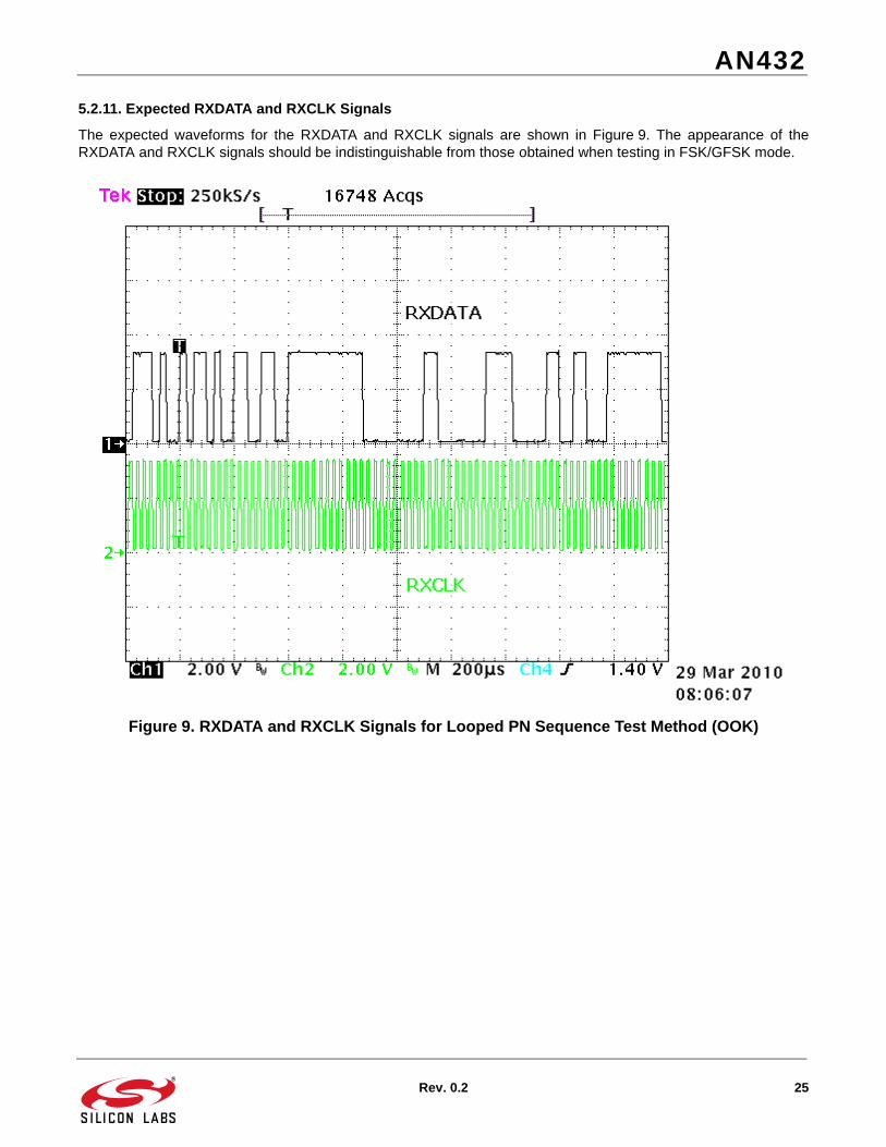
5.2.11. Expected RXDATA and RXCLK Signals
The expected waveforms for the RXDATA and RXCLK signals are shown in Figure 9. The appearance of theRXDATA and RXCLK signals should be indistinguishable from those obtained when testing in FSK/GFSK mode.
Figure 9. RXDATA and RXCLK Signals for Looped PN Sequence Test Method (OOK)

AN432
26 Rev. 0.2
DOCUMENT CHANGE LIST
Revision 0.1 to Revision 0.2 Added section describing measurements with
continuous preamble.
Added section describing measurements with PN sequence in OOK mode.
Added figures showing hardware test setups.
Added plots showing measured data.
Updated example WDS scripts.

AN432
Rev. 0.2 27
NOTES:

DisclaimerSilicon Laboratories intends to provide customers with the latest, accurate, and in-depth documentation of all peripherals and modules available for system and software implementers using or intending to use the Silicon Laboratories products. Characterization data, available modules and peripherals, memory sizes and memory addresses refer to each specific device, and "Typical" parameters provided can and do vary in different applications. Application examples described herein are for illustrative purposes only. Silicon Laboratories reserves the right to make changes without further notice and limitation to product information, specifications, and descriptions herein, and does not give warranties as to the accuracy or completeness of the included information. Silicon Laboratories shall have no liability for the consequences of use of the information supplied herein. This document does not imply or express copyright licenses granted hereunder to design or fabricate any integrated circuits. The products must not be used within any Life Support System without the specific written consent of Silicon Laboratories. A "Life Support System" is any product or system intended to support or sustain life and/or health, which, if it fails, can be reasonably expected to result in significant personal injury or death. Silicon Laboratories products are generally not intended for military applications. Silicon Laboratories products shall under no circumstances be used in weapons of mass destruction including (but not limited to) nuclear, biological or chemical weapons, or missiles capable of delivering such weapons.
Trademark InformationSilicon Laboratories Inc., Silicon Laboratories, Silicon Labs, SiLabs and the Silicon Labs logo, CMEMS®, EFM, EFM32, EFR, Energy Micro, Energy Micro logo and combinations thereof, "the world’s most energy friendly microcontrollers", Ember®, EZLink®, EZMac®, EZRadio®, EZRadioPRO®, DSPLL®, ISOmodem ®, Precision32®, ProSLIC®, SiPHY®, USBXpress® and others are trademarks or registered trademarks of Silicon Laboratories Inc. ARM, CORTEX, Cortex-M3 and THUMB are trademarks or registered trademarks of ARM Holdings. Keil is a registered trademark of ARM Limited. All other products or brand names mentioned herein are trademarks of their respective holders.
http://www.silabs.com
Silicon Laboratories Inc.400 West Cesar ChavezAustin, TX 78701USA
Simplicity StudioOne-click access to MCU tools, documentation, software, source code libraries & more. Available for Windows, Mac and Linux!
www.silabs.com/simplicity
MCU Portfoliowww.silabs.com/mcu
SW/HWwww.silabs.com/simplicity
Qualitywww.silabs.com/quality
Support and Communitycommunity.silabs.com