Embed Size (px)
Citation preview
Volume 55, Number 10, 2001 APPLIED SPECTROSCOPY 13370003-7028 / 01 / 5510-1337$2.00 / 0q 2001 Society for Applied Spectroscopy
Rugged Fiber-Optic Raman Probe for ProcessMonitoring Applications
PENTTI NIEMELA* and JANNE SUHONENVTT Electronics, P.O. Box 1100, FIN-90571 Oulu, Finland
We report on the development of a simple, rugged � ber-optic probefor process Raman measurements, in which laser line rejection isbased on an absorptive longpass � lter made from a direct bandgapCdTe semiconductor. The probe can be used with a � xed wave-length laser at 830 nm, and Raman spectra can be recorded downto 200 cm21 from the laser line. The � lter thickness can be adjustedfor � nal turning of the � lter edge, as the edge slope is almost in-dependent of thickness in the range 0.1 to 1 mm. Other propertiesof the probe, such as its signal-to-noise ratio and signal-to-back-ground ratio, are shown to compare well with those of a state-of-the-art probe based on holographic notch � lter techniques.
Index Headings: Raman spectroscopy; Fiber-optic probe; Bandgap� lter; Cadmium telluride.
INTRODUCTION
The possibility of using standard telecommunication� bers for remote sensing, combined with a high degreeof selectivity in spectral analysis, makes Raman spec-troscopy a versatile tool for process monitoring applica-tions. A simple � ber-optic probe may be just a bundle of� bers, the center � ber conducting the laser excitation tothe sample and the surrounding � bers serving as collec-tors of Raman scattering.1,2 However, if the � bers are longand/or the sample is not transparent, more sophisticatedprobes with adequate � ltering in the probe head are need-ed.3 A bandpass � lter must be used to eliminate Ramanscattering generated in the excitation � ber and a bandrejection � lter used to eliminate the laser radiation re-� ected back from the sample. Good overlap of the ex-citation and collection beams in the sample has beenachieved with a coaxial design of the probe head. Thesame focusing lens is used for both beams, and the beampaths are combined via a beamsplitter in the collimatedregion of the head. Single excitation and collection � bersare normally used in commercial implementations ofthese probes.3
Special requirements must be placed on the � lters andon the beamsplitter, which is usually of the dichroic type.Two main approaches are used in commercial probes, onemade by InPhotonics, which has only dielectric interfer-ence � lters, and a device of Kaiser Optical Systems thathas only volume holographic components.3 Better per-formance of the probe has been obtained with the newholographic � lters than with dielectric � lters, which arein any case of special design and not commonly avail-able. The holographic notch � lter, for example, has ahigher optical density at the laser wavelength, a steepercut-on slope, and better transmission above it. In the Kai-ser probe a notch � lter is also used as the beamsplitter,
Received 26 February 2001; accepted 4 June 2001.* Author to whom correspondence should be sent.
but at a small incident angle.3 The rejection band of anotch � lter is, however, very narrow and the band posi-tion is dependent on incident angle and � lter temperature,which can cause problems when the � lters are used inhostile environments.
A semiconductor bandgap � lter is an interesting can-didate for laser line rejection. A direct bandgap semicon-ductor has a sharp absorption edge, and a thin disk canserve as an ideal longpass � lter, having a steep cut-onslope and almost in� nite attenuation below that. A groupof direct-gap semiconductors, which have an absorptionedge in the wavelength range of lasers commonly usedin Raman excitation, is formed by the cadmium chalco-genides: CdS, CdSe, and CdTe.4 To our knowledge, veryfew examples of bandgap � lters used in Raman mea-surements can be found in the literature, possibly due inpart to the dif� culty of � nding a suitable laser for each� lter. Schulte et al. solved the problem by using a tunableTi:sapphire laser with a CdTe single crystal, and theywere able to measure Raman spectra within less than 100cm21 of the laser line by adjusting it close to the bandedge.5,6
We demonstrate in this paper the feasibility of using aCdTe bandgap � lter in Raman measurements with a � xedwavelength diode laser at 830 nm, describe a rugged � -ber-optic probe based on this � lter, and compare its per-formance with that of a state-of-the-art probe based onholographic notch � lter techniques.
EXPERIMENTAL
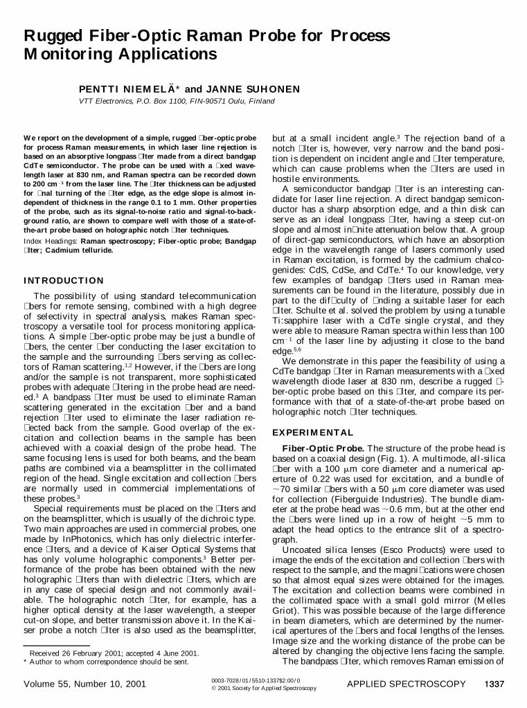
Fiber-Optic Probe. The structure of the probe head isbased on a coaxial design (Fig. 1). A multimode, all-silica� ber with a 100 mm core diameter and a numerical ap-erture of 0.22 was used for excitation, and a bundle of;70 similar � bers with a 50 mm core diameter was usedfor collection (Fiberguide Industries). The bundle diam-eter at the probe head was ;0.6 mm, but at the other endthe � bers were lined up in a row of height ;5 mm toadapt the head optics to the entrance slit of a spectro-graph.
Uncoated silica lenses (Esco Products) were used toimage the ends of the excitation and collection � bers withrespect to the sample, and the magni� cations were chosenso that almost equal sizes were obtained for the images.The excitation and collection beams were combined inthe collimated space with a small gold mirror (MellesGriot). This was possible because of the large differencein beam diameters, which are determined by the numer-ical apertures of the � bers and focal lengths of the lenses.Image size and the working distance of the probe can bealtered by changing the objective lens facing the sample.
The bandpass � lter, which removes Raman emission of
1338 Volume 55, Number 10, 2001
FIG. 1. Schematic diagram of the � ber-optic probe head. BR is a bandrejection � lter, BP a band pass � lter, and M stands for mirrors.
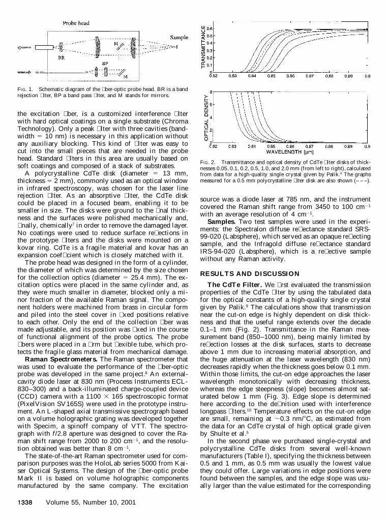
FIG. 2. Transmittance and optical density of CdTe � lter disks of thick-nesses 0.05, 0.1, 0.2, 0.5, 1.0, and 2.0 mm (from left to right), calculatedfrom data for a high-quality single crystal given by Palik.9 The graphsmeasured for a 0.5 mm polycrystalline � lter disk are also shown (– – –).
the excitation � ber, is a customized interference � lterwith hard optical coatings on a single substrate (ChromaTechnology). Only a peak � lter with three cavities (band-width 5 10 nm) is necessary in this application withoutany auxiliary blocking. This kind of � lter was easy tocut into the small pieces that are needed in the probehead. Standard � lters in this area are usually based onsoft coatings and composed of a stack of substrates.
A polycrystalline CdTe disk (diameter 5 13 mm,thickness 5 2 mm), commonly used as an optical windowin infrared spectroscopy, was chosen for the laser linerejection � lter. As an absorptive � lter, the CdTe diskcould be placed in a focused beam, enabling it to besmaller in size. The disks were ground to the � nal thick-ness and the surfaces were polished mechanically and,� nally, chemically7 in order to remove the damaged layer.No coatings were used to reduce surface re� ections inthe prototype � lters and the disks were mounted on akovar ring. CdTe is a fragile material and kovar has anexpansion coef� cient which is closely matched with it.
The probe head was designed in the form of a cylinder,the diameter of which was determined by the size chosenfor the collection optics (diameter 5 25.4 mm). The ex-citation optics were placed in the same cylinder and, asthey were much smaller in diameter, blocked only a mi-nor fraction of the available Raman signal. The compo-nent holders were machined from brass in circular formand piled into the steel cover in � xed positions relativeto each other. Only the end of the collection � ber wasmade adjustable, and its position was � xed in the courseof functional alignment of the probe optics. The probe� bers were placed in a � rm but � exible tube, which pro-tects the fragile glass material from mechanical damage.
Raman Spectrometers. The Raman spectrometer thatwas used to evaluate the performance of the � ber-opticprobe was developed in the same project.8 An external-cavity diode laser at 830 nm (Process Instruments ECL-830–300) and a back-illuminated charge-coupled device(CCD) camera with a 1100 3 165 spectroscopic format(PixelVision SV165S) were used in the prototype instru-ment. An L-shaped axial transmissive spectrograph basedon a volume holographic grating was developed togetherwith Specim, a spinoff company of VTT. The spectro-graph with f /2.8 aperture was designed to cover the Ra-man shift range from 2000 to 200 cm21, and the resolu-tion obtained was better than 8 cm21.
The state-of-the-art Raman spectrometer used for com-parison purposes was the HoloLab series 5000 from Kai-ser Optical Systems. The design of the � ber-optic probeMark II is based on volume holographic componentsmanufactured by the same company. The excitation
source was a diode laser at 785 nm, and the instrumentcovered the Raman shift range from 3450 to 100 cm21
with an average resolution of 4 cm21.Samples. Two test samples were used in the experi-
ments: the Spectralon diffuse re� ectance standard SRS-99-020 (Labsphere), which served as an opaque re� ectingsample, and the Infragold diffuse re� ectance standardIRS-94-020 (Labsphere), which is a re� ective samplewithout any Raman activity.
RESULTS AND DISCUSSION
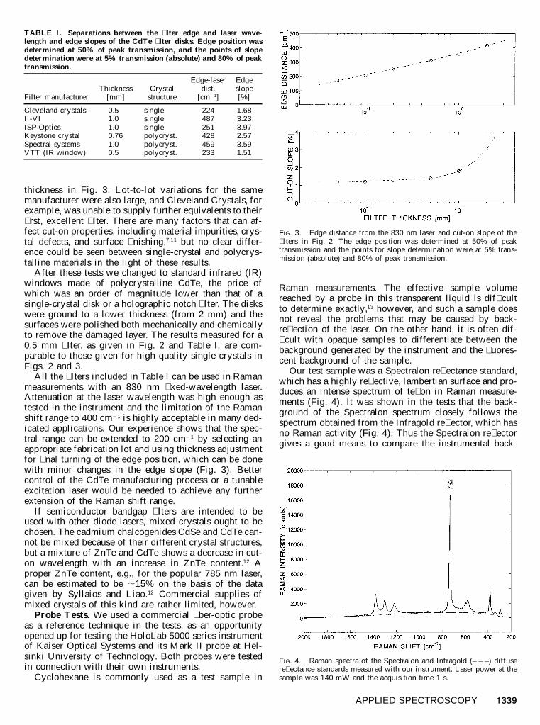
The CdTe Filter. We � rst evaluated the transmissionproperties of the CdTe � lter by using the tabulated datafor the optical constants of a high-quality single crystalgiven by Palik.9 The calculations show that transmissionnear the cut-on edge is highly dependent on disk thick-ness and that the useful range extends over the decade0.1–1 mm (Fig. 2). Transmittance in the Raman mea-surement band (850–1000 nm), being mainly limited byre� ection losses at the disk surfaces, starts to decreaseabove 1 mm due to increasing material absorption, andthe huge attenuation at the laser wavelength (830 nm)decreases rapidly when the thickness goes below 0.1 mm.Within those limits, the cut-on edge approaches the laserwavelength monotonically with decreasing thickness,whereas the edge steepness (slope) becomes almost sat-urated below 1 mm (Fig. 3). Edge slope is determinedhere according to the de� nition used with interferencelongpass � lters.10 Temperature effects on the cut-on edgeare small, remaining at ;0.3 nm/8C, as estimated fromthe data for an CdTe crystal of high optical grade givenby Shulte et al.5
In the second phase we purchased single-crystal andpolycrystalline CdTe disks from several well-knownmanufacturers (Table I), specifying the thickness between0.5 and 1 mm, as 0.5 mm was usually the lowest valuethey could offer. Large variations in edge positions werefound between the samples, and the edge slope was usu-ally larger than the value estimated for the corresponding
APPLIED SPECTROSCOPY 1339
TABLE I. Separations between the � lter edge and laser wave-length and edge slopes of the CdTe � lter disks. Edge position wasdetermined at 50% of peak transmission, and the points of slopedetermination were at 5% transmission (absolute) and 80% of peaktransmission.
Filter manufacturerThickness
[mm]Crystal
structure
Edge-laserdist.
[cm21]
Edgeslope[%]
Cleveland crystalsII-VIISP OpticsKeystone crystalSpectral systemsVTT (IR window)
0.51.01.00.761.00.5
singlesinglesinglepolycryst.polycryst.polycryst.
224487251428459233
1.683.233.972.573.591.51
FIG. 3. Edge distance from the 830 nm laser and cut-on slope of the� lters in Fig. 2. The edge position was determined at 50% of peaktransmission and the points for slope determination were at 5% trans-mission (absolute) and 80% of peak transmission.
FIG. 4. Raman spectra of the Spectralon and Infragold (– – –) diffusere� ectance standards measured with our instrument. Laser power at thesample was 140 mW and the acquisition time 1 s.
thickness in Fig. 3. Lot-to-lot variations for the samemanufacturer were also large, and Cleveland Crystals, forexample, was unable to supply further equivalents to their� rst, excellent � lter. There are many factors that can af-fect cut-on properties, including material impurities, crys-tal defects, and surface � nishing,7,11 but no clear differ-ence could be seen between single-crystal and polycrys-talline materials in the light of these results.
After these tests we changed to standard infrared (IR)windows made of polycrystalline CdTe, the price ofwhich was an order of magnitude lower than that of asingle-crystal disk or a holographic notch � lter. The diskswere ground to a lower thickness (from 2 mm) and thesurfaces were polished both mechanically and chemicallyto remove the damaged layer. The results measured for a0.5 mm � lter, as given in Fig. 2 and Table I, are com-parable to those given for high quality single crystals inFigs. 2 and 3.
All the � lters included in Table I can be used in Ramanmeasurements with an 830 nm � xed-wavelength laser.Attenuation at the laser wavelength was high enough astested in the instrument and the limitation of the Ramanshift range to 400 cm21 is highly acceptable in many ded-icated applications. Our experience shows that the spec-tral range can be extended to 200 cm21 by selecting anappropriate fabrication lot and using thickness adjustmentfor � nal turning of the edge position, which can be donewith minor changes in the edge slope (Fig. 3). Bettercontrol of the CdTe manufacturing process or a tunableexcitation laser would be needed to achieve any furtherextension of the Raman shift range.
If semiconductor bandgap � lters are intended to beused with other diode lasers, mixed crystals ought to bechosen. The cadmium chalcogenides CdSe and CdTe can-not be mixed because of their different crystal structures,but a mixture of ZnTe and CdTe shows a decrease in cut-on wavelength with an increase in ZnTe content.12 Aproper ZnTe content, e.g., for the popular 785 nm laser,can be estimated to be ;15% on the basis of the datagiven by Syllaios and Liao.12 Commercial supplies ofmixed crystals of this kind are rather limited, however.
Probe Tests. We used a commercial � ber-optic probeas a reference technique in the tests, as an opportunityopened up for testing the HoloLab 5000 series instrumentof Kaiser Optical Systems and its Mark II probe at Hel-sinki University of Technology. Both probes were testedin connection with their own instruments.
Cyclohexane is commonly used as a test sample in
Raman measurements. The effective sample volumereached by a probe in this transparent liquid is dif� cultto determine exactly,13 however, and such a sample doesnot reveal the problems that may be caused by back-re� ection of the laser. On the other hand, it is often dif-� cult with opaque samples to differentiate between thebackground generated by the instrument and the � uores-cent background of the sample.
Our test sample was a Spectralon re� ectance standard,which has a highly re� ective, lambertian surface and pro-duces an intense spectrum of te� on in Raman measure-ments (Fig. 4). It was shown in the tests that the back-ground of the Spectralon spectrum closely follows thespectrum obtained from the Infragold re� ector, which hasno Raman activity (Fig. 4). Thus the Spectralon re� ectorgives a good means to compare the instrumental back-
1340 Volume 55, Number 10, 2001
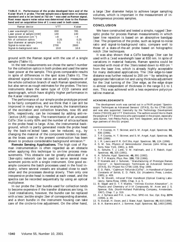
TABLE II. Performance of the probe developed here and of theKaiser Mark II probe. The test sample was a Spectralon re� ectancestandard and a te� on band at 732 cm 21 was used as Raman signal.Root mean square noise value was determined close to the Ramanband and an acquisition time of 1 s was used in both cases.
Raman device VTT Kaiser
Laser wavelength [nm]Laser power at sample [mW]Spectral resolution [cm21]NA of collection opticsSpot diameter at sample [mm]Signal-to-noise ratioSignal-to-background ratio
830140#8
0.250.5
270019.8
785140;4
0.250.1
260016.6
ground with the Raman signal with the use of a singlesample (Table II).
In the test measurements we chose the same f-numberfor the collection optics in both probes and used the samelaser power at the sample. This gives comparable resultsin spite of differences in the spot sizes (Table II). Theobtained signal-to-noise ratios are actually measures ofthe whole collection branch of each Raman spectrometer,but also serve as rough estimates for the probes. The twoinstruments share the same type of CCD camera andspectrograph, which have slightly higher performance inthe Kaiser instrument.
The performance of our simple probe prototype provedto be fairly competitive, and we think that it can still beimproved in many ways. For example, the transmittanceof the excitation and collection branches, now 65 and50%, respectively, can be increased by adding anti-re-� ective (AR) coatings. The transmittance of an uncoatedCdTe � lter is only 60% and the number of silica surfacesin the probe head is large. Also, the instrumental back-ground, which is partly generated inside the probe headby the back-re� ected laser, can be reduced, e.g., bychanging the material of the component holders to steel,as the brass used in the present construction has beenshown to produce considerable background emission.14
Remote Sensing Applications. The high cost of Ra-man instrumentation is often regarded as an obstaclewhen applying this technique to on-line process mea-surements. This obstacle can be greatly alleviated if a� ber-optic network can be used to serve several mea-surement points with a single instrument. One good ex-ample concerns the batch processes used in the food in-dustry, where several vessels are situated close to eachother and the processes develop slowly. Then only oneinexpensive probe head is needed at each vessel, and thespectra can be recorded sequentially by using an opticalmultiplexer.
In our probe the � ber bundle used for collection tendsto become expensive if the transfer distances are long. In� xed installations, however, the bundle can be replacedwith a less � exible single � ber of corresponding diameter,and a short bundle in the instrument housing can takecare of the circle-to-line adjustment. On the other hand,
a large � ber diameter helps to achieve larger samplingvolumes, which is important in the measurement of in-homogeneous process samples.
CONCLUSION
We have constructed and tested a simple, rugged � ber-optic probe for process Raman measurements in whichlaser line rejection is based on an absorptive bandgap� lter. The properties of the probe, such as signal-to-noiseratio and signal-to-background ratio, compare well tothose of a state-of-the-art probe based on holographicnotch � lter techniques.
It was also shown that a CdTe bandgap � lter can beused with a � xed wavelength laser at 830 nm. In spite ofvariations in material features, Raman spectra could berecorded with most of the � lters tested down to 400 cm21
from the laser line, which is already highly acceptablefor many dedicated applications. The � lter edge-to-laserdistance was further reduced to 200 cm21 by selecting anappropriate fabrication lot and using thickness adjustmentfor the � nal turning of the � lter edge, as the edge slopeis almost independent of thickness in the range 0.1 to 1mm. This was achieved with a less expensive polycrys-talline material.
ACKNOWLEDGMENTS
The development work was carried out in a FAIR project ‘Spectro-scopic Techniques as Advanced Sensors’ (STAS), Eu No CT96-1169,and was also supported � nancially by the Technology DevelopmentCentre (TEKES) and VTT Electronics. The authors would like to thankthe people at VTT Electronics who participated in the project, especiallyJuha Sumen, Veli-Pekka Putila, and Tomi Seppanen, and also the for-eign partners of this EU project.
1. T. F. Cooney, H. T. Skinner, and S. M. Angel, Appl. Spectrosc. 50,836 (1996).
2. T. F. Cooney, H. T. Skinner, and S. M. Angel, Appl. Spectrosc. 50,849 (1996).
3. I. R. Lewis and P. R. Grif� ths, Appl. Spectrosc. 50, 12A (1996).4. S. M. Sze, Physics of Semiconductor Devices (John Wiley and
Sons, New York, 1981), p. 849.5. A. Schulte, T. J. Lenk, V. M. Hallmark, and J. F. Rabolt, Appl.
Spectrosc. 45, 325 (1991).6. A. Schulte, Appl. Spectrosc. 46, 891 (1992).7. D. T. F. Marple, Phys. Rev. 150, 728 (1966).8. P. Niemela and J. Suhonen, ‘‘Manufacturing of Prototype Raman
Device’’, in Spectroscopic Techniques as Advanced Sensors(STAS), EU Project No CT96-1169, May 1999.
9. E. D. Palik, ‘‘Cadmium Telluride (CdTe)’’, in Handbook of OpticalConstants of Solids, E. D. Palik, Ed. (Academic Press, London,1985), p. 409.
10. D. W. Morelli, Infrared Filter Handbook (Optical Coating Labo-ratory, Santa Rosa, 1998), Chap. 3, p. 5.
11. B. Segall and D. T. F. Marble, ‘‘Intrinsic Exciton Absorption’’, inPhysics and Chemistry of II-VI Compounds, M. Aven and J. S.Spencer, Eds. (North-Holland Publishing Company, Amsterdam,1967), Chap. 7, p. 319.
12. A. J. Syllaios and P.-K. Liao, Proc. SPIE-Int. Soc. Opt. Eng. 2274(1994), p. 49.
13. N. Everall, H. Owen, and J. Slater, Appl. Spectrosc. 49, 610 (1995).14. B. A. Barrera and A. J. Sommer, Appl. Spectrosc. 52, 1483 (1998).