Embed Size (px)
DESCRIPTION
Tektronix RTSA Demo Board User Manual.
Citation preview

RTSA Version 3 Demo BoardUser Manual
*P077103800*077-1038-00


RTSA Version 3 Demo BoardUser Manual
www.tektronix.com077-1038-00

Copyright © Tektronix. All rights reserved. Licensed software products are owned by Tektronix or its subsidiariesor suppliers, and are protected by national copyright laws and international treaty provisions. Tektronix productsare covered by U.S. and foreign patents, issued and pending. Information in this publication supersedes that in allpreviously published material. Specifications and price change privileges reserved.
TEKTRONIX and TEK are registered trademarks of Tektronix, Inc.Contacting TektronixTektronix, Inc.14150 SW Karl Braun DriveP.O. Box 500Beaverton, OR 97077USA
For product information, sales, service, and technical support:
■ In North America, call 1-800-833-9200.
■ Worldwide, visit www.tektronix.com to find contacts in your area.

Table of ContentsPreface ................................................................................................................................................ iii
Preventing electrostatic damage .................................................................................................... iv
Board descriptionUser interface .................................................................................................................................. 2Waveform generation ..................................................................................................................... 2Waveform storage ........................................................................................................................... 2Internal waveform memory ............................................................................................................ 3Baseband I and Q capabilities ........................................................................................................ 3Sample clock division ..................................................................................................................... 3USB power source .......................................................................................................................... 4Specifications .................................................................................................................................. 4
Installation
OperationSignal indicators ............................................................................................................................. 8Controls .......................................................................................................................................... 8Inputs - Outputs .............................................................................................................................. 9
Modulation and waveformsStandard waveforms ..................................................................................................................... 11Waveform details .......................................................................................................................... 12
CW (Waveform 1) ................................................................................................................... 12INFREQUENT HOP (Waveform 2) ....................................................................................... 12CW PULSE (Waveform 3) ...................................................................................................... 14LFM PULSE (Waveform 4) .................................................................................................... 14PULSE TRAIN (Waveform 5) ................................................................................................ 16QPSK1 (Waveform 6) ............................................................................................................. 18QPSK2 (Waveform 7) ............................................................................................................. 18OFDM (Waveform 8) .............................................................................................................. 19AM (Waveform 9) ................................................................................................................... 20FM (Waveform 10) ................................................................................................................. 20SPECMON - INTERFERENCE (Waveform 11) ................................................................... 21ZERO SPAN (Waveform 12) .................................................................................................. 22
RTSA V3 Demo Board i

SETTLING TIME (Waveform 13) ......................................................................................... 23SPUR SEARCH (Waveform 14) ............................................................................................ 24P25 C4FM (Waveform 15) ...................................................................................................... 24P25 HPCM (Waveform 16) ..................................................................................................... 25Waveform 17 - 20 (undefined) ................................................................................................ 25
AdjustmentsPotentiometer descriptions ........................................................................................................... 28Calibration mode signals .............................................................................................................. 28Internal I-Q offset and gain adjustment ........................................................................................ 29External I-Q offset and gain adjustment ....................................................................................... 29
Table of Contents
ii RTSA V3 Demo Board

PrefaceThe Tektronix RTSA Version 3 demo board provides signals that you can use todemonstrate key features of Tektronix series spectrum analyzers.
The RTSA Version 3 demo board supersedes earlier versions of RTSA demoboards and is significantly different from the version 1 and version 2 boards.
This board was designed to:
■ Make some of the waveforms more useful when demonstrating RSA features.
■ Add more waveforms to use for demonstrating newer measurements on theRSA.
■ LFM pulses, for IPR demonstrations.
■ AM and FM waveforms for demonstrating audio analysis.
■ A basic OFDM signal that could be used “out of the box”.
■ Waveform(s) for demonstrating DPX zero span and DPXOgramdisplays.
■ Settling time demonstration waveform(s).
RTSA V3 Demo Board iii

■ Add a noise source that can be used directly with the RSA for noise figuretesting demonstrations.
■ Allow for future enhancements, additional waveforms.
■ Extra waveform slots – create your own waveforms.
■ External I/Q modulation inputs.
■ Ability to modify built-in waveforms without sending the unit back.
Preventing electrostatic damageElectrostatic discharge (ESD) can damage components on the demo board. Toprevent ESD:
■ Do not touch exposed components or connector pins unless you are usingESD protective measures, such as wearing an antistatic wrist strap.
■ Handle the demo board as little as possible.
■ Do not slide the demo board over any surface.
■ Transport and store the demo board in a static-protected bag or container.
Preface
iv RTSA V3 Demo Board

Board description
RTSA V3 Demo Board 1

User interfaceThe version 3 demo board uses 5 push button switches to select the operatingmode and the waveforms. LEDs are used to indicate the selected waveform andoperating mode.
Waveform generationThe previous RSA demo boards used an FPGA to algorithmically create I and Qsignals fed to the modulator. Since modifying the waveforms always required a“return to the factory”, adding new signals or changing signals was problematic.The version 3 demo board implements the most useful signals (except CW, Inf.Hop, and RF Pulse) found on the version 2 demo board as I and Q samples,which are then “played back” through DACs to the modulator. In other words,the board is a “mini-AWG” with RF modulation capability.
The CW, Inf. Hop, and RF Pulse signals are implemented in an FPGA, tosimplify certain aspects of those signals.
Waveform storageAll waveforms are stored in binary files on a microSD card to make thewaveforms easy to modify without turning the board into a USB memory device(prohibited in some secure areas). Modifying the waveforms is as simple asremoving the microSD card, copying new waveforms onto the card via PC andUSB adapter, and re-installing the microSD card.
Waveforms which are stored as part of the FPGA algorithms (CW, Inf. Hop, RFPulse) do not have I and Q waveform files on the microSD card. However, thewaveforms can be modified by adding waveforms to the microSD Card withappropriate filenames.
Board description
2 RTSA V3 Demo Board

Internal waveform memoryWaveforms on the microSD card are packed in a binary format, which is thencopied directly to SDRAM when a new waveform is selected. A waveform ismade up of 1 to 64 segments, each of which can be repeated up to 4 billion times.This allows for very long waveforms to be created without requiring immenseamounts of SDRAM.
Baseband I and Q capabilitiesIn addition to the I and Q input ports on the Version 1 and 2 demo boards, theversion 3 board also has I and Q outputs. Each of these outputs can also be usedfor baseband LF signals (such as audio tones).
Excessive LO leakage was seen on some version 1 and version 2 demo boards.To correct this, I & Q gain and I & Q offset adjustments are including in theversion 3 board. Refer to the Adjustment section for details on how to minimizeLO leakage through the modulator.
Sample clock divisionThe basic sample rate for both I and Q sample streams is 24.576 MHz. For eachwaveform this sample rate can be divided by two up to 10 times (24.576 MHz /2^10 = 24 kHz). Since the board does not have a variable-bandwidthreconstruction filter, this means that copies (alias signals) are present at theoutput for all but the base 24.576 MHz sample rate. This should not be aproblem, since the demonstration procedure for the various waveforms reducesthe acquisition bandwidth (“Spans down on the signal”) providing the necessaryreconstruction filtering within the RSA itself.
An easy way to think about this is that the demo board always outputs a signalwith 10 MHz bandwidth, but in cases where the sample clock is divided only partof that bandwidth is the “good” part of the signal.
Board description
RTSA V3 Demo Board 3

USB power sourceThe version 3 demo board requires power from two USB 2.0 ports (total of~750 mA at 5 Volts). The Y-cable provided must have both USB-A plugs to beconnected to powered USB 2.0 ports before connecting the USB-B plug to thedemo board and powering on. USB ports may become disabled when excessivepower is drawn from the port, depending on the system implementation.
And, of course, the demo board may also be powered by an external 5 V supplycapable of delivering at least 750 mA. A USB wall-charger for phones is a goodsubstitute.
Specifications
Characteristic DescriptionInputs I and Q baseband input 0-5 MHz, 1 Vp-p, 50 Ω
Noise source bias input 0V (disable) or +28V (enable), 17 mA nominalUSB-B power input 800 mA minimum
Outputs RF output Amplitude -5 dBm ±1 dBm into 50 ΩFrequency 2.445312 GHz nominalFrequencyAccuracy
±100 ppm (-10 °C to +55 °C), ± 20 ppm nominal at 20 °C
ModulationBW
10 MHz nominal
Noise output 20 dB ENR (10 MHz to 3 GHz), 50 ΩI and Q basebandoutputs
DC – 5 MHz, 3 dB bandwidth±100 mV nominal (-10 dBm) into 50 ΩOutput levels are dependent on EXT I/Q INPUT levels when EXT is selected.
Waveform Storage 20 waveforms1 to 64 repeatable segments per waveformMaximum 32 Msamples per waveform, not including segment repetitions
Board description
4 RTSA V3 Demo Board

Installation
1. Plug the dual USB A connectors from one end of the “Y” USB cable into twoUSB ports of the RSA or your PC. Make this connection before plugging theother end of the cable in to the USB B connector on the Demo board.
2. Plug the single USB B connector into the B-connector on the Demo board.
3. Use a 50 Ω BNC cable to connect the RF OUT of the Demo board to the RFIN connector on your RSA Signal Analyzer.
NOTE. This connection may require an N-to-BNC adapter (103-0045-XX).
4. Press the ON/OFF button on the demo board. The red LED near this buttonwill light.
NOTE. If you turn on the demo board, and just one of the two USB Aconnectors is attached to the RSA or PC, you may cause an over-currentlimit (>500 mA) condition. This can generate an error message on the PC,and requires a system reboot to clear.
RTSA V3 Demo Board 5

Installation
6 RTSA V3 Demo Board

Operation
RTSA V3 Demo Board 7

Signal indicatorsUpon initial power-on, the top four Signal LEDs in each column alternately showthe FPGA version and FW version (coded in Hex format). The left column is MSnibble, row 1 is LSB, row 4 is MSB.
After ~4 seconds, a single LED indicates the selected waveform.
Controls
ON/OFF Power Switch (LED is Red when power is ON). Controls power to the board.
ROW/COLUMN Selects desired signal, as indicated by the LEDs in the SIGNALS section.
■ ROW – pressing this button repetitively cycles through waveform selectionrows 1-10, moving one row per button press.
■ COLUMN – pressing this button alternates the selected column.
Waveform loading begins ~2 seconds after selection. The signal selection LEDblinks at a rate of about 1 Hz while the waveform is loading from the MicroSDcard into RAM.
Signal output at RF Out initiates as soon at waveform loading is complete. (Theselected signal LED will be constant ON.)
INT / EXT Selects the modulation source.
■ INT – Selects internal signals / modulation (internal waveforms).■ EXT – Selects EXTERNAL I/Q modulation inputs.■ OFF – Output is switched OFF.
RUN MODE Selects how the waveforms are output.
■ FREERUN – Waveforms are continuously output.■ SINGLE – Provides a single instance / pulse output of the waveform. The
TRIGGER control generates the single instance.
When in SINGLE mode, the TRIGGER LED blinks at about a 1 Hz rate toindicate it’s waiting for a trigger event.
Operation
8 RTSA V3 Demo Board

TRIGGER Pressing this button generates a single waveform instance of the selectedwaveform at the RF output when the Run Mode is set to SINGLE.
Inputs - Outputs
USB Power (USB BConnector)
Connect the supplied USB “Y” cable to two USB A ports on an RSA, PC, orUSB HUB.
This is compatible with USB 1.x, 2.x, and 3.0.
Used for power only (and future remote control capabilities).
28V IN / NOISE OUT This is for use with the RSA5100 Series or RSA6100 Series instruments withOption 14 (Gain and Noise Figure Measurements).
Connect the 28V IN to the 28 V Output BNC located on the rear panel of anRSA5100 Series or RSA6100 Series instrument (draws ~17 mA). The LED lightsBLUE when the 28V source is enabled from the RSA instrument.
Connect the NOISE OUT to the DUT. Refer to specification section (in thisdocument) for the output level. Refer to the RSA instrument’s documentation fornoise source usage.
EXTERNAL I / Q INPUT Use these inputs when you want to create your own modulation at the RF OUTport.
These baseband I/Q inputs drive the RF modulator directly when EXT isselected, providing the modulation on the 2.4453GHz carrier.
The INT / EXT control button must be set to EXT.
Refer to specification section (in this document) for the input requirements.
BASEBAND I / Q OUTPUT Provides I and Q output and is always enabled, regardless of the INT/EXTsetting. Refer to specification section (in this document) for the outputspecifications.
RF OUT Provides the RF signal output. Refer to specification section (in this document).
Connect this BNC to your RSA analyzer input using a 50 Ω cable.
Operation
RTSA V3 Demo Board 9

Operation
10 RTSA V3 Demo Board

Modulation and waveformsThe Demo board waveforms have two groups, External and Internal modulations.
■ External modulations
■ The user provides the baseband modulation via cables to theEXTERNAL I/Q inputs.
■ The DACS are set for zero output and are not changed.
■ Modulation switches are switched to external.
■ Internal modulations
These are the Standard Waveforms. Standard waveforms on page 11
■ FPGA-based
These are coded in the FPGA
■ ARB memory
■ These waveforms are stored in MicroSD card memory in proprietarybinary format.
■ Stored waveforms are loaded from SD card to RAM, then playbackcommences.
■ Waveforms may be changed / overwritten on the MicroSD card, butmust conform to the proprietary file standard. Contact your TektronixAE for details.
Standard waveformsThe list below indicates the standard waveforms by signal number. Waveforms 1,2, 3, and 13 are generated by the FPGA.
NOTE. Waveforms 1, 2, 3, and 13 can be overridden by the presence of therelevant bin file on the Micro SD Card (e.g. 01.bin, 02.bin, 03.bin, and/or 13.bin)
Waveforms 1-13 are general-purpose, and are intended to match the waveformsexpected in the demo guides. Waveforms 15-20 are expansion slots usedprimarily for standards-based waveforms. At the time of initial board releasewaveforms 15 and 16 are allocated to P25 demo waveforms. Waveform 8 wasoriginally designed to be an OFDM signal independent of standard, but 802.11pwas chosen for the description of this waveform.
Refer to the RSA306 demo guide (071-3330-xx) for details on how to use thesesignals in demonstrations of RSA306 features and capabilities.
RTSA V3 Demo Board 11

Table 1: List of signals
WFM # Signal Name1 CW 11 SPECMON2 Infrequent Hop 12 Zero Span3 CW Pulse 13 Settling Time4 LFM Pulse 14 Spur Search5 Pulse Train 15 Waveform 15 ( P25 C4FM)6 QPSK1 16 Waveform 16 (P25 HCPM)7 QPSK2 17 Waveform 178 OFDM (802.11p) 18 Waveform 189 AM 19 Waveform 1910 FM 20 Waveform 20
Waveforms are selected by pressing the ROW and COLUMN buttonsrespectively.
Waveform detailsThis section provides details about each signal available on the Demo board.
CW (Waveform 1) ■ Continuous 2445.312 MHz sine wave output, -5 dBm
■ Q DAC is fixed at zero volts.
INFREQUENT HOP(Waveform 2)
This waveform is a -5 dBm CW signal centered at 2445.312 MHz.
Every 1.28 seconds, the frequency will hop to 2458.2 MHz for approximately155 μs.
Use this signal to demonstrate DPX (vs. spectrum “Max Hold”), Spectrogram,frequency vs. time, and Frequency Mask Trigger.
■ Starting frequency: 2445.312 MHz
■ Hop frequency: 2458.2 MHz (+12.9 MHz approximate)
■ Overshoot peak deviation: 2.83 MHz (approximate)
NOTE. The damped waveform should peak at 2460.4 MHz positive,2442.3 MHz negative.
■ Overshoot damping time constant: ~15 μs
■ Hop duration: ~155 μs
■ Cycle period: 1.28 sec.
Modulation and waveforms
12 RTSA V3 Demo Board

Figure 1: INF HOP Frequency vs. Time Display with markers
Figure 2: INF HOP signal DPX display
Modulation and waveforms
RTSA V3 Demo Board 13

CW PULSE (Waveform 3) This waveform is a pulsed CW signal, centered at 2445.312 MHz.
PRI is 100 μs - Pulse ON duration is 10 μs, OFF duration is 90 μs.
Use this waveform to demonstrate RF power trigger, Pulse measurements (option20).
■ Carrier Wave: 2445.312 MHz■ Pulse on width: 10 μs■ Pulse off width: 90 μs■ Pulse ON power: -5 dBm■ On/OFF ratio: >40 dB■ Risetime, falltime: 60 ns
Figure 3: CW Pulse waveform
LFM PULSE (Waveform 4) This waveform is a Linear Frequency Modulated RF Pulse waveform, centered at2445.312 MHz.
PRI is 250 μs -Pulse on duration is 25 μs, off duration is 225 μs.
While the pulse is ON, the frequency of the signal is varied linearly from2440.312 MHz to 2450.312 MHz.
Use this waveform to demonstrate RF power trigger, Frequency Mask trigger,Frequency vs. Time measurement, Pulse measurements (option 20)
■ Carrier Wave: 2445.312 MHz■ Linear chirp: 10 MHz sweep■ PRI: 250 μs■ Pulse on width: 25 μs duty cycle is 10%
Modulation and waveforms
14 RTSA V3 Demo Board

■ Pulse off width: 225 μs
■ Pulse ON power: -5 dBm
■ On/OFF ratio: > 40 dB
■ On/OFF ratio: > 40 dB
■ Frequency deviation: ±5 MHz about 2445.312 MHz
Figure 4: LFM Pulse spectrum
Figure 5: LFM frequency vs. time plot
Modulation and waveforms
RTSA V3 Demo Board 15

PULSE TRAIN(Waveform 5)
Two 100-pulse patterns separated by 5 ms and repeated once every second. Eachpulse train consists of 100 CW pulses with a full amplitude I DAC output.
Pulse Pattern #1: 100 1 μs pulses at a fixed PRI of 100 μs. 51st pulse is -20 dBdown (i.e. a runt).
Figure 6: Pulse pattern #1
Figure 7: Close up of the "runt" pulse in the middle of pulse pattern #1
Pulse Pattern #2: First pulse is 20 μs wide and the remaining 99 pulses are 1 μswide. PRI ramps from 96 μs to 103 μs and then back down to 96 μs.
Modulation and waveforms
16 RTSA V3 Demo Board

Figure 8: Pulse pattern #2, long pulse
Use this waveform to demonstrate runt trigger, time qualified triggers, Pulsemeasurements (option 14).
Figure 9: Pulse pattern spectrum
Modulation and waveforms
RTSA V3 Demo Board 17

QPSK1 (Waveform 6) Pre-programmed QPSK waveform (QPSK1).
■ Carrier Wave: 2445.312 MHz
■ Symbol rate: 3.072 MS/S
■ Pattern: PRBS9
■ Filter: RRC, alpha=0.33
■ EVM: < 5%
Noise bandwidth used for EVM calculation: 1 kHz to 1.5 MHz.
Figure 10: QPSK1 waveform
QPSK2 (Waveform 7) Pre-programmed QPSK waveform (QPSK2).
■ Carrier Wave: 2445.312 MHz
■ Symbol rate: 3.84 MS/S
■ Pattern: PRBS11
■ Filter: RRC, alpha=0.22
■ EVM: < 5%
Noise bandwidth used for EVM calculation: 1 kHz to 2 MHz.
Modulation and waveforms
18 RTSA V3 Demo Board

Figure 11: QPSK2 signal
OFDM (Waveform 8) 802.11p standard 10 MHz wide OFDM packet that repeats every 2 ms.
■ Carrier Wave: 2445.312 MHz
■ OFDM EVM, RMS all: better than -23 dB
Figure 12: OFDM 802.11p waveform
Modulation and waveforms
RTSA V3 Demo Board 19
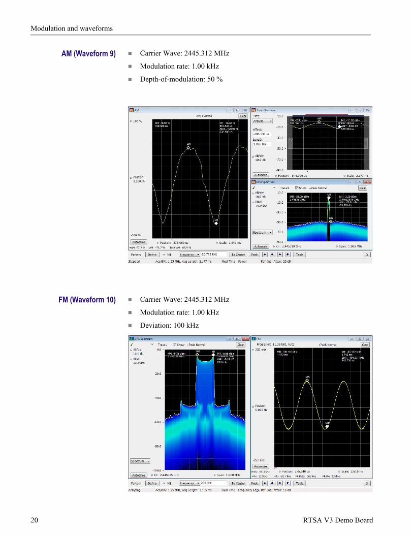
AM (Waveform 9) ■ Carrier Wave: 2445.312 MHz
■ Modulation rate: 1.00 kHz
■ Depth-of-modulation: 50 %
FM (Waveform 10) ■ Carrier Wave: 2445.312 MHz
■ Modulation rate: 1.00 kHz
■ Deviation: 100 kHz
Modulation and waveforms
20 RTSA V3 Demo Board

SPECMON -INTERFERENCE
(Waveform 11)
Continuous 10 MHz LFM Pulse superimposed with a FM signal -40 dB down.
LFM Pulse Description:
■ Carrier Wave: 2445.312 MHz
■ Linear chirp: 10 MHz sweep
■ Chirp on width: 1 ms
■ Chirp off width: ~0
■ On/OFF ratio: > 40 dB
■ Frequency deviation: ± 5 MHz about 2445.312 MHz
FM Description:
■ Carrier Wave: 2445.312 MHz
■ Frequency Offset: 3 MHz
■ Modulation rate: 1.00 kHz
■ Deviation: 2 MHz
Modulation and waveforms
RTSA V3 Demo Board 21

ZERO SPAN(Waveform 12)
Zero Span cycles through four waveforms approximately every 125 μs. Eachwaveform is played for roughly 25 μs. Resulting PRI is about 150 μs. Thewaveforms in order are a 10 MHz wide LFM pulse, a 10 MHz QPSK PRBS9waveform, an AM modulated waveform with a 1 MHz modulating frequency at10% depth, and a FM waveform with a 1 MHz modulating frequency and a 50%modulation index.
LFM Pulse Description:
■ Carrier Wave: 2445.312 MHz
■ Linear chirp: 10 MHz sweep
■ Chirp on width: 25 μs
■ Frequency deviation: ± 5 MHz about 2445.312 MHz
QPSK Waveform Description:
■ Carrier Wave: 2445.312 MHz
■ Symbol rate: 3.072 MS/S
■ Pattern: PRBS9
■ Filter: RRC, alpha=0.33
■ EVM: < 3%
AM Waveform Description:
■ Carrier Wave: 2445.312 MHz
■ Modulation rate: 1.00 MHz
■ Depth-of-modulation: 10 %
FM Waveform Description:
■ Carrier Wave: 2445.312 MHz
■ Modulation rate: 1.00 MHz
■ Deviation: 500 kHz
Modulation and waveforms
22 RTSA V3 Demo Board

Figure 13: Zerospan waveform
SETTLING TIME(Waveform 13)
This signal is the same as Infrequent Hop (Waveform 2) signal described above.
Figure 14: Settling time
Modulation and waveforms
RTSA V3 Demo Board 23

SPUR SEARCH(Waveform 14)
Two-tone waveform with tones at +1 MHz and +4 MHz relative to the centerfrequency of 2445.312 MHz
■ 4 MHz tone is -50 dB down relative to 1 MHz tone.
Figure 15: SPUR search
P25 C4FM (Waveform 15) P25 standard continuous C4FM signal with a bandwidth of 12.5 kHz.
Figure 16: P25 C4FM waveform
Modulation and waveforms
24 RTSA V3 Demo Board

P25 HPCM (Waveform 16) P25 standard continuous HCPM (Inbound) signal with a bandwidth of 12.5 kHz
■ Symbol rate is 4800 Symbols/sec.
■ Modulation fidelity for P25 HPCM ~24%
Figure 17: P25 HPCM waveform
Waveform 17 -20 (undefined)
Waveforms 17 through 20 are currently unused waveform slots that default tocarrier wave signals at 2445.312 MHz.
Modulation and waveforms
RTSA V3 Demo Board 25

Modulation and waveforms
26 RTSA V3 Demo Board

AdjustmentsThere are eight adjustments to be made to adjust the offset/gain into the I/Qmodulator, and minimize the carrier feedthrough. These are divided into twogroups: Internal I/Q and External I/Q.
The Internal I/Q adjustments have been made at the factory. The External I/Qadjustments should be made if you're using External I/Q modulation inputs.
RTSA V3 Demo Board 27

Potentiometer descriptions■ Internal I Gain, Internal Q Gain
Varies amplitudes ±0.6 dB via potentiometer Initial setting nulls LOfeedthrough at the modulator when internal input is selected and DAC=3FF.
■ Internal I offset, Internal Q Offset
Varies “DC” offset voltage ±2% of full scale via 20-turn potentiometer Initialsetting nulls LO feedthrough at the modulator when internal input is selectedand DAC=0.
■ External I Gain, External Q Gain
Varies amplitudes ±0.6 dB via potentiometer Initial setting nulls LOfeedthrough at the modulator when external input is selected and inputV=0.5 VDC.
■ External I offset, External Q Offset
Varies “DC” offset voltage ±2% of full scale via 20-turn potentiometer Initialsetting nulls LO feedthrough at the modulator when external input is selectedand DAC=0.
Calibration mode signalsWhen the calibration-mode jumper is added, waveforms 00, 01, 02, and 03 areoutput.
These waveforms are scrolled normally using the waveform Row toggle switch.
Table 2: Calibration mode signals
Location Name Description00 OFF Used to null carrier leakage
through the modulator01 Full-scale I, Q is off Used to check I-channel
magnitude02 Full-scale Q, I is off Used to check Q-channel
magnitude03 Full-scale I plus full-scale Q Used to verify full scale output
amplitude Same as Waveform1, CW.
Adjustments
28 RTSA V3 Demo Board

Internal I-Q offset and gain adjustment1. Set up INTERNAL cal mode, internal CW signal OFF.
■ Select “INTERNAL” mode via push-button switch.
■ Select “Calibration” mode by moving jumper J14 to the CAL position.
■ Select calibration waveform 00 (CW = signal OFF) using the ROWbutton.
■ Connect the RF output BNC to the RSA input.
■ Set the RSA CF to 2.4453GHz, Ref Level -10 dBm.
■ Add a marker to the residual signal at 2.4453 GHz (press PEAK to addmarker).
2. Adjust INTERNAL I Gain & Offset.
■ Adjust R40, INTERNAL_I_GAIN_ADJUST (labelled IIG), so that the2445.3 MHz carrier residual output is minimized.
■ Adjust R25, INTERNAL_I_OFFSET (labelled IIO) to minimize theresidual carrier – this is a 20-turn pot, so be patient to see the effect.
3. Adjust INTERNAL Q Gain & Offset.
■ Adjust R42, INTERNAL_Q_GAIN_ADJUST (labelled IQG), so that the2445.3 MHz residual carrier output is minimized.
■ Adjust R26, INTERNAL_Q_OFFSET (labelled IQO) to minimize theresidual carrier – this is a 20-turn pot, so be patient to see the effect.
4. Re-check INTERNAL I/Q Gain and Offset.
■ Adjusting the I & Q gain and offset are interactive will alter the outputresidual level slightly.
■ Steps 1 & 2 should be repeated at this point for the final offset null.
External I-Q offset and gain adjustment1. Adjust External I Gain and offset.
■ Terminate EXTERNAL_I and EXTERNAL_Q BNC inputs with 50 ΩBNC terminations.
■ Select EXT (external) mode via the INT/EXT push-button switch.
Adjustments
RTSA V3 Demo Board 29

■ Monitor the 2445.3 MHz output on a spectrum analyzer.
■ Adjust R49, EXTERNAL I OFFSET ADJUST (labelled EIO), and R48,EXTERNAL_I_GAIN_ADJUST (labelled EXT_I_GAIN), so that the2445 MHz output is minimized.
2. Adjust EXTERNAL Q Gain and offset.
■ Select EXT (external) mode via the INT/EXT push-button switch.
■ Adjust R51, EXTERNAL_Q_GAIN_ADJUST (labelledEXT_Q_GAIN), and R52 EXTERNAL_Q_OFFSET_ADJUST (labelledEQO) to minimize the 2445 MHz output.
3. Re-check EXTERNAL I/Q DC offset.
■ Adjusting the gain will alter the offset slightly.
■ Steps 1 & 2 should be repeated at this point for the final offset null.
Adjustments
30 RTSA V3 Demo Board