Embed Size (px)
Citation preview
RAINBOWTECHNOLOGY SYSTEMS
the new coater-laminator for liquid resistThe proprietary coating system and resist from RTS allows manufacturers new freedoms to create high package density circuitry - fine lines with ultra thin layers. RTS resist can be used both as an etch resist and a pattern plating resist.
Using a combination of electroless copper, electrolytic copper, etch resist and standard solder masks, layers can be built sequentially. This method avoids the need for lay up/bonding press, and drilling. Cost reductions are significant based on having 30% fewer processes. Additionally, 3D features can be created around the circuitry and the starting point can be a rigidiser - not necessarily copper laminate.
Each layer can be as thin as 10 microns (conductive and insulating combined) so a ten layer assembly might only be 100 microns thick. Registration is achieved by a simple jig system. Imaging is achieved by a combination of UV printing (lithographic or DI) and laser ablation which defines the minimum sizes of features that can be obtained. Via holes less than 1.00mm are easily achievable. The process could be automated as required and lends itself to flexible and rigid assemblies/printed electronics.
RTS CL
No VOCsCoating thickness: 2 - 30 micron (controllable)
Fine line printing for easier developing and etchingExcellent conformity enhances adhesion, reducing risk of open circuits
Coating takes place in controlled cleanroom environment at ambient temperatureNo pre-heat or heater rollers requiredResist does not foam in plating bathsLow energy requirement at imaging
Tenting capability comparable to dry filmDI / LDI / Photolithographic imaging
For panels and webs
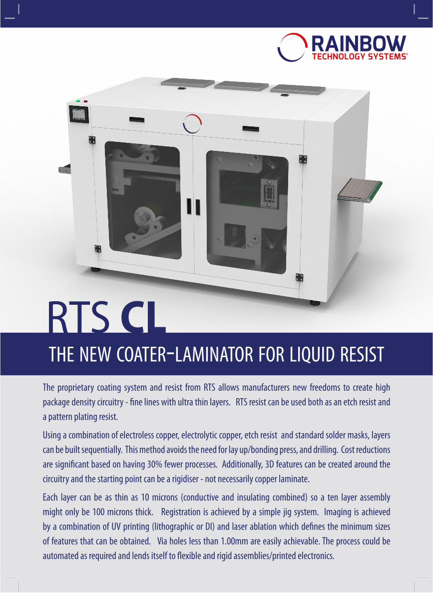
print circuits or prepare panels for imaging
Rainbow Technology Systems Ltd40 Kelvin Avenue, Hillington Park, Glasgow, G52 4LT
T: (+44)141 892 3320 W: www.rainbow-technology.com E: [email protected]