Embed Size (px)
Citation preview

RTDS Training Course of IEPG DAY 6: MMC and HVDC Example
COORDINATOR: DR. IR. J.L. RUEDA TORRES
RESPONSIBLE FOR LAB INSTRUCTIONS: DR.IR. DA WANG, IR. LIAN LIU
2018
1. Introduction
The objective of this lab session is to provide a practical overview of the Modular Multi-
Level Converter (MMC) technology in order to build a basic point-to-point High Voltage
Direct Current (HVDC) link based on this type of Voltage Source Converter (VSC)
technology. Nowadays, there are several approaches to develop an MMC model, and
each of them can vary depending on the application and studies to be performed. In Part
1 of this document, a brief introduction of this VSC converter type is provided. A control
philosophy of the MMC is introduced as well, which basically is divided between upper
level and lower level control structures. Afterwards, all the modelling approaches
(defined by CIGRE) of VSC converters are illustrated. Then, the available model in
RTDS is explained. An illustrative case of a point-to-point MMC-based HVDC link (i.e.
DCS1 of CIGRE) is demonstrated in Part 2.
Note: This document is provided with a simple model in RTDS. You are expected to
follow the instructions provided in this tutorial and carry out the specified tasks. At the
end of this tutorial, you should:
a. Understand the principle of operating an MMC converter.
b. Design the MMC converter based on user-defined function.
2. Prerequisite Knowledge
From previous lab sessions:
You should be familiar with building/modifying RSCAD draft cases.
You should be able to run basic RTDS cases.
3. Attached folders
Draft and sib files for DSC1 system. The cli and clo files which are required for the
frequency dependent model of the DC cable in RTDS.
Part 1
1. Introduction of the VSC Converter
Due to the advancement of high power semiconductors (i.e. controllable switches),
HVDC technology has considerably evolved from Line-Commutated Converters
(thyristor-based technology) to VSC technology (Insulated-Gate Bipolar Transistor,
IGBT-based technology). The last one (VSC technology), has also evolved (in the last
two decades), from two- and three-level systems to MMC systems. The two- and three-
level converters are considered by the HVDC engineers as the first generations of VSC
systems (also called “classic” VSC systems). In the “classic” VSC systems, Pulse Width
Modulation (PWM) is used in order to create the respective voltage waveforms to
transmit power between the networks coupled to the converter stations. However, these
voltage waveforms have to be filtered due to the very high harmonic content.
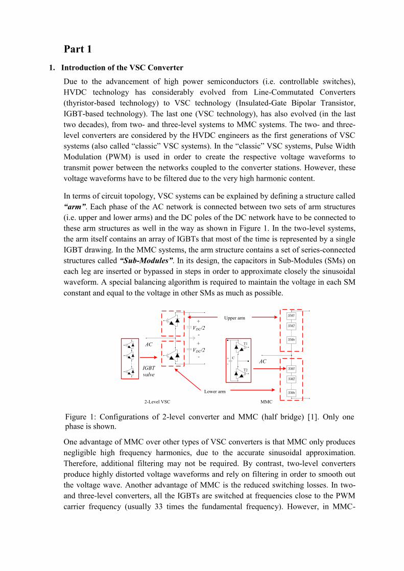
In terms of circuit topology, VSC systems can be explained by defining a structure called
“arm”. Each phase of the AC network is connected between two sets of arm structures
(i.e. upper and lower arms) and the DC poles of the DC network have to be connected to
these arm structures as well in the way as shown in Figure 1. In the two-level systems,
the arm itself contains an array of IGBTs that most of the time is represented by a single
IGBT drawing. In the MMC systems, the arm structure contains a set of series-connected
structures called “Sub-Modules”. In its design, the capacitors in Sub-Modules (SMs) on
each leg are inserted or bypassed in steps in order to approximate closely the sinusoidal
waveform. A special balancing algorithm is required to maintain the voltage in each SM
constant and equal to the voltage in other SMs as much as possible.
One advantage of MMC over other types of VSC converters is that MMC only produces
negligible high frequency harmonics, due to the accurate sinusoidal approximation.
Therefore, additional filtering may not be required. By contrast, two-level converters
produce highly distorted voltage waveforms and rely on filtering in order to smooth out
the voltage wave. Another advantage of MMC is the reduced switching losses. In two-
and three-level converters, all the IGBTs are switched at frequencies close to the PWM
carrier frequency (usually 33 times the fundamental frequency). However, in MMC-
+
VDC/2
-
+
VDC/2
-
AC
IGBT
valve
AC
SM1
SM2
SMn
SM1
SM2
SMn
T1
T2
C+
-
2-Level VSC MMC
Upper arm
Lower arm
Figure 1: Configurations of 2-level converter and MMC (half bridge) [1]. Only one
phase is shown.

based systems the switching frequency of each IGBT is only a few times the
fundamental frequency (1 to 3 times). In addition, the gate firing system is highly
reliable and effective.
A typical VSC HVDC station is shown in Figure 2, in which there are other basic
elements beside VSC converters [1]:
Phase reactors: Phase reactors are required at the VSC’s AC terminals to allow for
active and reactive power control. In two-level VSC converters, phase reactors are
also sized to help limit the ripple current at the AC side caused by PWM switching
below an acceptable level.
AC filter: Shunt high-pass filter branches are required to eliminate switching
harmonics from the AC voltage. The filter is essential in 2- and 3-level VSC
converters. Depending on the number of steps and the size of the cell capacitors they
might or might not be required in multilevel converters.
Transformer: The transformer works as interface between VSC and the AC system; it
adapts the grid voltage to a suitable level for the VSC. The transformer can also
provide a second stage of ripple current attenuation.
DC capacitors: The primary purpose of DC capacitors is to limit the DC voltage ripple
within a predefined permissible limit, particularly when PWM switching is applied.
These capacitors are strictly necessary in two-level converters. However, in multilevel
converters they might not be necessary to obtain low ripple DC voltages, since the
cell capacitors in SMs on six arms also serve as energy storage elements on the DC
side. The DC capacitor can also function as an energy storage element that helps
maintaining the power balance during transient events.
2. Operating principle of the MMC converter
The half-bridge sub-module of this type of converter is depicted in Figure 1. T1 and T2
are two insulated-gate bipolar transistors or gate turn-off thyristors (i.e. IGBTs or GTOs)
controlling the bypassing or inserting of the capacitor in the sub-module, thus the output
voltage of the SM is either 0 or the capacitor voltage VC. During insertion, the AC
current flows through the capacitor and T2 or its anti-paralleled diode to enable energy
exchange. Meanwhile, during bypass, the AC current can only flow through T1 or its
anti-paralleled diode. These two states together with their output voltages are depicted in
VSC
converter
AC Filter
Transformer Phase Reactor
+
uCabc
-
+
uSabc
-
iabc
R L
DC
Capacitors
Figure 2: A Typical VSC HVDC converter.

Figure 3. The block state is only used for the initial capacitor charging state and for
protection purposes during AC or DC faults. Under this situation, the current can only
flow through the diode that is anti-paralleled with T1.
It needs to be mentioned here that the anti-parallel diode of T1 provides a path for the
alternating current when a SM is bypassed, while that of T2 offers a charging path for the
capacitor, which is not an ideal voltage source. The increasing voltage in Figure 3 shows
the charging, which is regulated by a specific capacitor voltage balancing algorithm.
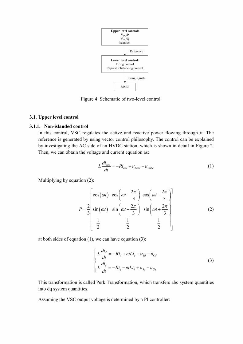
3. The MMC converter control
Two-level control is typical for the VSC, and it is implemented for MMC as well. The
upper level of control generates the reference voltage wave dependent on the VSC’s
control mode, i.e. DC voltage/active power, AC voltage/reactive power or islanded
control mode. Based on the higher hierarchical reference, the lower level control
provides valve firing signals and ensures that each cell capacitor voltage remains
constant according to a predetermined value. The schematic of two-level control is
depicted in Figure 4.
T1
T2
C+
-
T1
T2
C+
-
iAC iAC
Insertion Bypass
Figure 3: Performances of SM during inserted and bypassed states [1].
3.1. Upper level control
3.1.1. Non-islanded control
In this control, VSC regulates the active and reactive power flowing through it. The
reference is generated by using vector control philosophy. The control can be explained
by investigating the AC side of an HVDC station, which is shown in detail in Figure 2.
Then, we can obtain the voltage and current equation as:
abcabc Sabc Cabc
diL Ri u u
dt (1)
Multiplying by equation (2):
2 2cos cos cos
3 3
2 2 2sin sin sin
3 3 3
1 1 1
2 2 2
t t t
P t t t
(2)
at both sides of equation (1), we can have equation (3):
dd q Sd Cd
q
q d Sq Cq
diL Ri Li u u
dt
diL Ri Li u u
dt
(3)
This transformation is called Perk Transformation, which transfers abc system quantities
into dq system quantities.
Assuming the VSC output voltage is determined by a PI controller:
Upper level control:
VDC/P
VAC/Q
Islanded
Lower level control:
Firing control
Capacitor balancing control
MMC
Reference
Firing signals
Figure 4: Schematic of two-level control

_
_
ICd p d ref d q Sd
ICq p q ref q d Sq
Ku K i i Li u
s
Ku K i i Li u
s
(4)
Then, substituting (4) into (3) yields:
_
_
d I Ip d p d ref
q I Ip q p q ref
di K KL R K i K i
dt s s
di K KL R K i K i
dt s s
(5)
The subscript “ref” means reference values or the set point of id and iq. Based on (5), the
typical decoupled inner current PI controller of the upper level control can be represented
by Figure 5. In the same figure, the outer controller is also shown, and it is used to
generate the reference currents automatically based on user-defined MMC operating
mode: id_ref is controlled by either the active power loop or a DC voltage loop, while iq_ref
is controlled by the reactive power loop or an AC voltage loop.
In the active power control loop, the changing rate of the power order (Pref) should be
limited to a pre-specified slope in order to achieve stable response of the controller.
Similarly, filters are designed to apply ramps to any changes in the orders of DC voltage,
AC voltage, and reactive power. Additionally, as a part of the VDC control mode, a
voltage droop factor has been integrated into the control loop, although it is not shown in
Figure 5. When operating under this mode, the droop will determine the power sharing
and the voltage levels of the terminals. These two loops help enhance the stability of the
HVDC systems.
3.2. Lower level control
The objective of the low-level control is to provide the firing orders to the cell IGBTs
such that a voltage wave form is reproduced according to the modulation indices from
Kp
Ki/s
++
+-
ωL Mqabc
to
dq
Kp
Ki/s
++++
ωLMd
MCa
MCb
MCc
+-
+-
FILTER
FILTER
iq_ref
id_ref
iq
id
dq
to
abc
Kp2
Ki2/s
++
Kp3
Ki3/s
++
Kp4
Ki4/s
++
Kp5
Ki5/s
++
ia
ib
ic
PLL
uSa
uSb
uSc
θPLL θPLL
FILTER
+-
+-
FILTER
FILTER
+-
+-
FILTER
VACa
VAC ref
Q
Qref
P
Pref
VDC
VDC ref
Outer Controller Inner Controller
+
+
uSq
uSd
1/Vacm
1/Vacm
Figure 5: Non-islanded upper level control

the upper level control, while balancing the cell capacitor voltages. This control strategy
determines which IGBT in each cell fires depending on two factors: first the requirement
for inserting or bypassing a cell, and second the direction of the current.
3.2.1. Circulating current suppression control
In lower level control, the capacitor voltages of all SMs are regulated within an
acceptable range: the SMs with lowest or highest capacitor voltages are switched in
according to the direction of the arm current. The regulated capacitor voltages are
variated and as a result, there are circulating currents among the three-phase units. The
circulating current can introduce extra power losses. It has been shown that for different
load phase angles, the circulating current is in negative sequence and its main frequency
is the second harmonic of the AC system.
This current does not influence the currents in the AC and DC sides, but they distort the
arm current and increase the rated current of the sub-modules, which will influence the
performance of the converter. In order to reduce the effects of circulating current, the
control loop is introduced as the one shown in Figure .
3.2.2. Capacitor voltage balancing
The final stage of the lower level controller is the capacitor balancing controller. For
MMC applications, the voltages of SM capacitors on an arm have to be maintained to the
similar level for successful operation. Therefore, the firing pulses must be generated
considerately.
A common method used in balancing the SM capacitor voltages is the sorting method.
This method can sort the magnitude of each SM capacitor voltage in one arm from
highest to lowest. Afterwards, based on the modulation indices, the lower level controller
will insert the SMs with the highest voltages to discharge when the arm current is
negative and insert the SMs with the lowest voltages to charge when the arm current is
positive. When all the capacitor voltages are monitored and sampled at a sufficient
frequency, the capacitors can be naturally balanced through this way.
4. Modelling an MMC converter
At present, the simulation in most electromagnetic transient software is based on
Dommel’s algorithm. The core of his algorithm is to solve following equation:
ipj
inj
++ 1/2 acb-dq0
2ωt
i2fd
i2fq
+-
-+
i2fd_ref=0
i2fq_ref=0
Kp
Ki/s +++
2ωL
2ωL
Kp
Ki/s ++-
dq0-acb
udiffd_ref
udiffq_ref
udiff_ref
Figure 6:Circulating current suppressing control loop

1 1N N N N
G V I (6)
in which [G] is the conductance matrix of the network, [V] is the given nodal voltage
vector, and [I] is the current vector. These matrices’ sizes are determined by N: the
number of electrical nodes in the system. In each time step, the simulated system is
divided into two sections: A contains the nodes with known voltages, while B contains
the nodes with unknown voltages. Then, equation (6) becomes:
1 1
AA AB A A
BA BB B BN N N N
G G V I
G G V I
(7)
From (7), the unknown voltage vector [VB] is obtained through:
BB B B BA AG V I G V (8)
and is recalculated in each time step. Although the inverse of matrix [GBB] is not
calculated directly, its size significantly influences the computing time of one time step,
as it solves [GBB]-1
using forward solution (or forward triangularisation) and back
substitution.
At present, there are six types of models serving for different grid studies. Among which,
the most simulating-efficient method to model MMC converter is the Type 4 model. This
model’s breakthrough is that it performs a drastic reduction of the electrical node number
based on Thevenin equivalents, as shown in Figure , which determines the nodal matrix
size of an MMC converter. More importantly, this model still reveals accurate impacts of
different capacitor voltages in each sub-module. Thus, real-time simulation of MMC-
based HVDC system is possible. All the suitable research scopes of the various MMC
models are listed in Table 1 [2].
SM1
SM2
SMn
T1
T2
C+
-
Req
Veq
∑Req
∑Veq
(a) (b)
Figure 7: Efficient modelling of MMC. (a) Equivalent circuit of one sub-module. (b)
Equivalent circuit of one arm

Table 1: Summary of model types
Type of model Relative computing time Type of simulation tools Type of research
Type 1 NA Circuit simulation tools Not suitable for grid studies
Type 2 1000
Detailed studies of faults in
submodules; Used to validate
simplified models
Type 3 900
Detailed studies of faults in
submodules; Used to validate
simplified models
Type 4 30
Detailed studies of faults in
submodules; Used to validate
simplified models
Type 5 2
Studies of AC and DC transients
– high level control system
design-harmonic studies
Type 6 1.5Studies of remote AC and DC
transients
Type 7 0.01 Power flow tools Power flow
EMT

Part 2 1. INTRODUCTION
This part describes a Half-Bridge (HB) MMC-based point-to-point HVDC link in RTDS.
All the control loops were demonstrated in Part 1, except the SM voltage balancing
algorithm: only step firing PWM is adopted.
2. The MMC models available in RTDS
There are four types of models of MMC-HVDC developed in the RTDS lab. The models
use a surrogate network topology which modifies the valve topology model but
maintains the accuracy of a real valve. The main benefit is the reduced computational
burden on the hardware. Details of the surrogate network topology will not be discussed
here. All models can be configured for half or full bridge topology.
2.1. rtds_vsc_FPGA_U5
The U5 model, shown in Figure , is a detailed equivalent valve model that requires
individual SM firing and uses switchable resistance to model the ON and OFF state of an
IGBT/Diode. An MMC valve provides opportunities for parallel computation. Once the
MMC valve current is calculated, each SM capacitor voltage can be calculated
independently from the other and can be solved in parallel. By establishing many parallel
paths for calculation, the computation time can be reduced and a smaller time step can be
achieved. The massive parallel processing capabilities of a Field-Programmable Gate
Array (FPGA) makes it the ideal hardware to model a detailed equivalent MMC valve.
As a result, the U5 valve is not modelled on the main RTDS processor cards rather a
dedicated MMC Support Unit hardware that consists of a Xilinx FPGA board. The
support unit is interfaced to the RTDS Simulator through ½ small time step Bergeron
travelling waves which is an extremely stable interface. The rtds_vsc_FPGA_U5 icon
supports up to three valves (or legs), either half bridge or full bridge and each valve can
include up to 512 SMs. Currently, the U5 valve can be modelled on MMC Support Unit
Figure 8: rtds_vsc_FPGA_U5 icon

V1 which consist of a Xilnix ML605 FPGA and MMC Support Unit V2 which consists
of a Xilnix VC707 FPGA. The ML605 FPGA board supports one U5 component which
results in the MMC Support Unit V1 to model up to three valves. The VC707 FPGA has
the added resources to model two U5 components simultaneously which results in the
MMC Support Unit V2 to model up to 6 valves.
2.2. rtds_vsc_MMC5
The rtds_vsc_MMC5, shown in Figure , is referred to as the simplified model because it
is less complex compared to the U5 model. This model assumes the capacitor voltages
of each SM are internally balanced and therefore does not require specifically
which SMs to insert, only requiring the number of SMs to be inserted. The control
input is simplified to an overall deblock integer signal and the number of SMs to be
inserted. The main use of this model is for testing upper level controls. The added benefit
is that less hardware is required. The MMC5 valve is modelled on the main RTDS PB5
processor. This model also includes the ½ small time step interface T-line despite the
fact that the valve is modelled on the small time step processor. The small time step
network maintains a constant conductance matrix and the addition of the interface line
decouples the valve model from the small time step network, which allows switchable
resistance to be used for IGBT/diodes.
2.3. rtds_vsc_MMC_GM
A second detailed equivalent model has been developed, referred to as the ‘General
Model’ (GM). The valve model is very similar to the U5 model with some key
differences. The main difference is that each SM IGBT switch can be controlled
individually which allows dead time to be generated during switching transitions.
This also allows the possibility to model more types of internal faults. The
capacitance of each SM can also be configured independently. This model carries a
Figure 9: rtds_vsc_MMC5 icon

larger computational burden compared to the U5 model and can only be simulated on the
MMC support Unit V2 hardware and each MMC Support Unit can model two valves.
More details on the model can be found in RTDS documentation.
2.4. rtds_vsc_MMCHF_FPGA2
The rtds_vsc_MMCHF_FPGA icon, shown in Figure , is an MMC low level controller
modelled on an MMC Support Unit. When using a detailed equivalent valve model, such
as the U5 and GM models, a lower level controller is necessary to convert the upper level
control output into firing pulses for each SM. Each valve requires its own low-level
control. The rtds_vsc_MMCHF_FPGA icon can support up to three controllers. Each
controller requires 3 inputs from the RTDS: Deblock word, integer for the number of
SMs to insert, and a real number threshold in kV for the allowed capacitor voltage range
before re-ranking is required. In addition, the valve controller will receive signals
directly from the MMC valve such as the SM capacitor voltages and valve current. The
controller will output the firing pulses directly to the MMC valve through fibres. Details
of the communication between the valve and controller can be found in RTDS
documentation. The MMCHF_FPGA icon can be modelled on both MMC Support Unit
V1 and V2. Using V1, the ML605 only supports up to 2 controllers. With V2, the VC707
board can support up to 3 controllers due to the added resources.
2.5. rtds_vsc_CHANV5
The CHAINV5 is a detailed equivalent MMC model and is simulated in the small time
step environment. A detailed equivalent model means that the internal electrical nodes
are eliminated and the MMC is modelled as a Norton’s equivalent as shown in Figure 11.
The capacitor voltage for each SM is calculated and firing pulses are required for each
Figure 10: rtds_vsc_MMCHF_FPGA2 icon

SM. Therefore, the CHAINV5 requires a low level capacitor balancing controller to
maintain the same voltage across all SMs in the valve. The CHAINV5 module is limited
to a maximum of 56 half bridge (~or 48 full bridge) SMs due to the computational
requirements for the model. Typically one CHAINV5 module is placed on a single
processor but that would depend on the number of SMs per valve.
Figure 11: rtds_vsc_CHAINV5 icon

Table 2: Converter station parameters
3. Point-to-point HVDC link description
3.1. System configuration
The system is a two-terminal symmetric monopole HVDC link. The draft canvas of the
example model is shown in Figure . The source at C1 (right one) represents an offshore
converter and is connected to the onshore terminal A1 by a DC cable.
The AC grids are modelled by equivalent sources with A1 and C1 grid voltages being
380 kV L-L RMSand 145 kV L-L RMS respectively. The source impedances for each
terminal have the following parameters:
A1: Rs=0.048 Ω, Ls=0.015 H, Rp=1000 Ω
C1: Rs=0.333 Ω, Ls=0.0175, Rp=1000 Ω
The converter station parameters are shown in Table 2.
As mentioned before, there are four types of MMC models in RTDS. Because the MMC
Support Unit hardware is not available, the U5, GM, and FPGA2 models are not applied
here but the MMC5 model is adopted for both converter A1 and C1. Each of them is
modelled in a separate bridge box, in the small time step environment. For accurate
transient responses, it is important to model the DC cable as a frequency dependent line
Figure 12: Point-to-point HVDC link

rather than a Bergeron line1. There is no frequency dependent travelling wave model in
the small time step library due to the calculation burden of this model. As a result, the
frequency dependent cable from the large time step library is used and interface t-lines
are inserted to connect the DC cable in the large time step to the DC side of the MMC
converter in the small time step. The interface line is a Bergeron model with an
approximate cable length of 10 km. The DC cable length was modified to compensate
for addition of the interface lines.
The upper level and lower level controllers are developed using the large time step
control system library. These controls for terminal A1 and C1 can be found in the
hierarchy box ‘A1 Controls’ and ‘C1 Controls’ respectively. Figure 13 shows the power
system layout inside terminal A1 VSC bridge box, which is exactly the same as the one
for terminal C1.
3.2. DC cable parameters
An XLPE cable is used for this test. As stated in the B4-57 working brochure, the data is
based on a +/- 320kV DC cable with insulation thickness adapted for +/- 200 kV which
is the DC rating of the system. The parameters are shown in Figure 1. The DC cable line
length is 200 km, but has been reduced to 183 km to compensate for the interface
transmission lines on both ends.
3.3. AC and DC protection
The test case encompasses basic protection against low AC voltage and DC overcurrent.
Figure shows the control circuit for low ac voltage protection. The control circuit
monitors the primary voltage and if the peak voltage drops below 0.1 pu (three-phase AC
1 The Bergeron model is based on a distributed LC parameter travelling wave line model, with lumped
resistance. It represents the L and C elements of a PI Section in a distributed manner (i.e. it does not use
lumped parameters). It is roughly equivalent to using an infinite number of PI Sections, except that the
resistance is lumped (1/2 in the middle of the line, 1/4 at each end).
Like PI Sections, the Bergeron Model accurately represents the fundamental frequency only. It also
represents impedances at other frequencies, except that the losses do not change. This model is suitable for
studies where the fundamental frequency load flow is most important (i.e. relay studies, load flow, etc.).
1
2
3 4
5
6
7
8
Figure 6: MMC converter terminal
1. AC Grid, 2. Three phase AC fault branch, 3. Pre-Insertion resistor, 4. Converter transformer, 5. Star
Reactor, 6. MMC valves (MMC5), 7. DC fault pole to pole branch, 8. Interface Transmission line.

LG Fault), a flag will be enabled that blocks the converter valves. The converter valves
will stay blocked until the AC voltage rises above 0.1 pu.
Figure is the control circuit for DC overcurrent protection. The control circuit will
enable a flag when the DC current goes above 6 kA for 0.0001 seconds. The flag signal
“FLTMODE’ will force the converters valves to block and open the main AC breakers.
Figure 74: Cable parameters
Figure 15: AC low voltage protection
Figure 16: Overcurrent DC protection

4. Results
The control modes and set points for the test case are:
Terminal A1
DC voltage control with DC reference = 1 pu (+/-200 kV)
Reactive power control with Q reference = 0 MVAR
Terminal C1
Active Power Control with P reference =400 MW (+ve flows into DC)
Reactive power control with Q reference =0 MVAR.
4.1. Steady state results
Figure 17 shows the AC and DC voltages and real and reactive power valves once the
system reaches steady state.
4.2. Transient results
Figure 18 shows the faults controls in RUNTIME.
The case has three types of fault scenarios.
1. AC LG fault on side A1
2. AC LG fault on side C1
3. Permanent pole-to-pole fault on side A1
There are three push buttons, as seen in Figure 19, that will enable each of these faults.
To enable the fault again, the fault command needs to be RESET which is done by
pushing the Reset push button that is associated with each fault command, as seen in
Figure 17. Steady state results
Figure 18. Fault control panel

Figure 19. The slider ‘ACFAULT’ sets the duration of the AC faults. The DC pole-to-
pole fault is considered permanent and has been set to a fixed duration that is long
enough such that the DC protection circuit has already responded. The DIAL sets the
type of AC fault. All type of AC faults are line to ground (LG) but the different phases
can be enabled as shown in Table 3.
4.2.1. 200ms 3-phase fault on side A1
When the AC voltage drops on the A1 side, the AC protection will block the A1
converter valves until the AC voltage rises above a certain threshold (0.1 pu). Once the
fault has ended and the AC voltage on side A rises above the threshold, A1 converter
valves will be deblocked and system should reach steady state. The transient response
will be heavily dependent on the configuration and parameters of the controls. See
Figure 19 and Figure 20 for the transient response of various signals.
4.2.2. DC pole-to-pole fault at A1 converter
The DC protection on both terminals will detect overcurrent (>6kA) and block their
converters and open their respective AC breaker. See Figure 21 for results during the DC
fault.
Table 3. Dial position and type of AC fault

Figure 19. 1) DC voltage. 2) DC current. 3) AC primary current. 4) Active and reactive
power
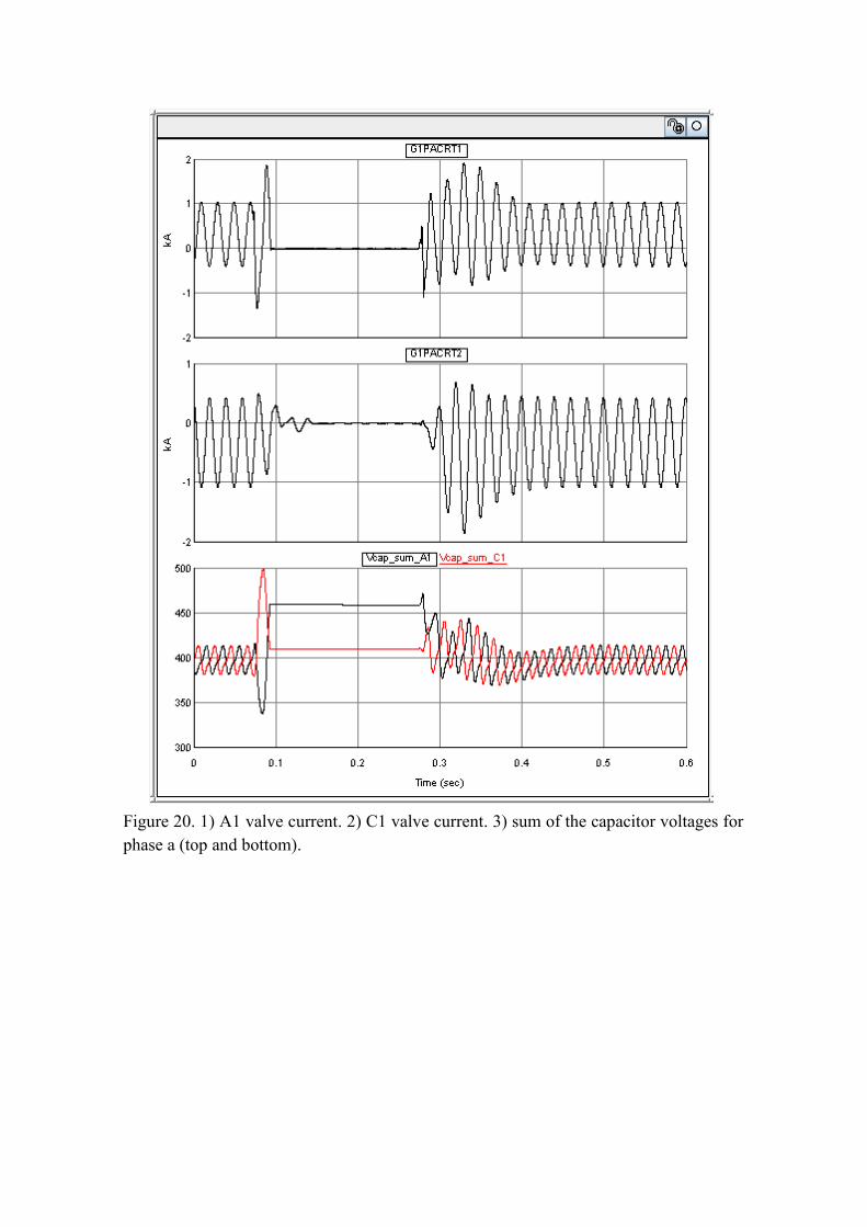
Figure 20. 1) A1 valve current. 2) C1 valve current. 3) sum of the capacitor voltages for
phase a (top and bottom).

Figure 21. 1) DC voltages 2) DC current 3) A1 AC primary currents
Reference [1] Lian Liu, PhD thesis “Protection of multi-terminal HVDC systems – algorithm
development and performance verification by EMT simulations” to be published.
[2] CIGRE Working Group B4.57, “Guide for the development of models for HVDC
converters in a HVDC grid.”