Embed Size (px)
Citation preview

S1
RSC Nanoscale
Supporting Information to
Tailoring Morphology and Structure of Tungsten Oxide
Nanoparticles for Inkjet Printed Electrochromic DevicesPawel Jerzy Wojcik*, Lidia Santos, Luis Pereira, Rodrigo Martins, Elvira Fortunato*
CENIMAT/I3N, Departamento de Ciência dos Materiais, Faculdade de Ciências e Tecnologia,
FCT, Universidade Nova de Lisboa (UNL), 2829-516 Caparica, Portugal, Fax: (+351) 21 294
8558, Tel: (+351) 21 294 8562
* Corresponding authors: [email protected] and [email protected]
Table of Contents
1. Strategy in metal oxide nanoparticle engineering for printed applications .........
2. Hydrothermal synthesis details …………………………………………………
3. Hydrothermal conditions ……………………………………………………….
4. Inkjet printing system …………………………………………………………..
5. Sample dimensions ……………………………………………………………..
6. Substrate cleaning procedure …………………………………………………...
7. Ink formulation details ………………………………………………………….
8. Optical measurements set-up …………………………………………………...
9. Definitions of parameters ………………………………………………………
10. Molecular crystal model ……………………………………………………..
11. 3D NPs Model development …………………………………………………..
12. Fourier Transform Infrared Spectroscopy …………………………………….
13. Simultaneous Thermal Analysis (TG-DSC) …………………………………..
14. Model of agglomeration for various regular shaped NPs ..................................
15. Influence of the film thickness on electrochemical response …………………
16. Spectral response ……………………………………………………………...
17. Graphics ……………………………………………………………………….
References …………………………………………………………………………
S2
S3
S4
S4
S6
S6
S7
S8
S12
S15
S16
S19
S20
S22
S23
S24
S25
S25
Electronic Supplementary Material (ESI) for Nanoscale.This journal is © The Royal Society of Chemistry 2014

S2
1. Strategy in metal oxide nanoparticle engineering for printed applications
To progress in the development of inkjet printed electrochromic (EC) devices, the problem has to
be considered in an interdisciplinary context. This means understanding and describing the
desired nanomaterial performance, as well as its technological and environmental requirements.
The strategy selected in this study is based on correlation of the nanoparticles (NPs) synthesis
parameters with further technological steps for ink formulation, film deposition, post-treatment
and resulting film performance, as it is schematically presented in Figure 1.
Figure S1. Simplified NPs process flow diagram for printed electrochemically active films;
factors closely associated with NPs properties were colored in green, while factors considered as
irrelevant were colored in red
To assure the desired electrochemical performance and processability, the criteria for NPs size,
crystallinity, morphology as well as the uniformity and agglomeration mechanism are going to
be established in following subsections, providing recommendations on each major technological
step and determine constraints, for the application of NPs specifically in printed dual-phase EC
films. However, presented here engineering rules for NPs synthesis and ink formulation have to a
large extend, universal character and may be implemented to create a variety of new inkjet

S3
printable nanostructured metal oxide (MOX) materials for chromic, photovoltaic, photocatalytic
and power storage applications.
2. Hydrothermal synthesis details
The hydrothermal synthesis was performed using Teflon-lined stainless steel autoclave (4745
general purpose vessel, Parr) and laboratory furnace with settable temperature profile
(L3/11/B170, Nabertherm) as it is presented in Figure S2. The starting material for WOX NPs
synthesis consisted of previously synthesized PTA dissolved in HCl aqueous solution just before
use. Prepared solution was transferred into PTFE chamber, set inside the stainless steel autoclave
and installed in the oven with temperature rising from RT up to 180 C, ramp rate 5 C/min,
for selected time of 120, 240 or 360 min.
Figure S2. Hydrothermal synthesis setup

S4
3. Hydrothermal conditions
The hydrothermal conditions for water based precursor can be approximated using well known
August-Roche-Magnus empirical formula expressed by equation S1.
(S1)𝑝(𝑇) = 𝑝0𝑒( 17.625𝑇𝑇 + 243.04)
where: p is saturation water vapor pressure in hPa, T is temperature in C, p0 is saturation water
pressure at T = 0 C ( hPa). The plot of water vapor pressure in function of 𝑝0 = 6.1094
temperature in a range of RT-220 C is presented in Figure S3.
Figure S3. Saturation water vapor pressure in function of temperature as an approximation of
conditions during hydrothermal synthesis
4. Inkjet printing system
A commercially available Canon PIXMA IP4500 desktop printer (Canon Virginia, Inc., Newport
News, USA) with a resolution of 9600×2400 dpi was used as the printing device. This thermal-
type printing unit allows deposition of the material by a digital printing process, where the
ink/material is ejected directly onto a substrate from 1536 nozzles (Magenta or Cyan channel)
driven by an electronic signal. The fabrication of the active layer by inkjet printing was
performed at room temperature and atmospheric pressure. Necessary modifications have been
carried on according to the instruction presented in Figure S4.

S5
Figure S4. Modifications applied to Canon PIXMA IP4850 desktop printer; presented
instruction is also valid for Canon PIXMA IP4500 used in present studies as inkjet printing
system for EC film deposition.

S6
The selection of inkjet printing system for experiments was dictated by the printer functionality,
which should satisfy several requirements. Firstly, the printer enables printing on CDs using
dedicated CD tray. Secondly, cartridges are not integrated with the printhead. Canon PIXMA
desktop printers compatible with CD printing were found to be the most suitable for this task.
Full tests were performed with models Canon PIXMA MP600 (tray F), IP4500 (tray F) and
IP4850 (tray G). However, there are many potentially useful models available which differ
mainly in CD printing tray used, for example:
tray B - IP3000, IP4000, IP5000, IP6000, IP6000D, IP8500, MP750, MP760, MP780;
tray C - IP4200, IP5200, IP6700D, MP950;
tray D - MP500, MP530, MP800, MP830;
tray E - Pro9000, Pro9500;
tray F - IP4300, IP5300, MP610, MP810, MX850, MP960, MP970;
tray G - MG5240, MG6140, MG6150, MG8140, MG8150, IP4600, IP4680, IP4700,
IP4780, IP4820, IP4840, MG8120, MG6120, MG6220, MG5320, MG5220, MG5250;
tray J - IP7200, MG6300, MG5400.
5. Sample dimensions
Optically active a-WO3/WOX films with area of 1 cm2 were printed in ITO PET stripes with
dimensions shown in Figure S5.
Figure S5. Sample dimensions
6. Substrate cleaning procedure
Following procedure was applied for ITO PET substrates cleaning:
a) Protection foil is removed from ITO PET surface just before cleaning procedure.
b) Both surfaces of ITO PET substrate are cleaned with lint free tissues and
isopropyl alcohol.

S7
c) First ultrasonic cleaning of substrates is performed in deionized water with 3%
glass detergent (Cleaner concentrate for cuvette washing, Fluka) for 10 minutes at
60ºC.
d) Substrates are thoroughly rinsed with deionized water.
e) Second ultrasonic cleaning is performed in deionized water for 10 minutes at 60
ºC.
f) Substrates are thoroughly rinsed with deionized water.
g) Third ultrasonic cleaning is performed in ethanol for 5 minutes at 60 ºC.
h) Substrates are thoroughly rinsed with deionized water.
i) The last step of ultrasonic cleaning is performed in isopropyl alcohol for 5
minutes at 60 ºC.
j) If necessary, substrates can be stored in isopropyl alcohol.
k) Just before use substrates are dried by nitrogen flow.
7. Ink formulation details
The WOX NPs loaded dispersions based on aqueous ethanol vehicle were subjected to ultrasonic
treatment using ultrasonic stand mounted homogenizer (Ultrasonic Compact Hielscher UP400S)
applied in ice cooled batch, as shown in Figure S6a. Sonication amplitude was applied according
to the profile shown in Figure S6b.
Figure S6. Ultrasonic procedure shown as a) schematic drawing and b) amplitude profile; 100 %
amplitude corresponds to 400 W ultrasonic (24 kHz, automatically tuned frequency) power;
cycle parameter was set as 0.5
Homogenizer was equipped with titanium sonotrode (dispersing tools) with tip diameter 3 mm,
length 100 mm and male thread M10×1 designed for samples ranging from 5 up to 200 ml.
S8
The viscosity of the ink can be easily increased to the acceptable level without substantially
modifying its other properties, by addition of thickening agents. For inorganic solid/liquid
mixtures, it can be a low boiling point, viscous and miscible with the vehicle organic solvent or
soluble polymer, e.g. (for aqueous ink) polyethylene glycol (PEG) or polyvinyl alcohol (PVA).
For surface tension adjustment of aqueous inks, the nonionic surfactant such as e.g. Triton X-100
or Triton X-45 can be added in amount of 0.1 - 0.5 wt%. In order to effectively disperse
nanomaterial powder in a vehicle, breaking of NPs agglomerates and stabilization by pH
modification, additions of surfactants or polymers are required. However, liquid medium
complexity may significantly deteriorate electrical performance of final printed films. Therefore,
in a perfect situation, NPs are dispersed in a pure water or aqueous alcoholic solution with no
other organic additives, which allows for low post-treatment temperature. Moreover, it is crucial
that the ink components are chemically compatible with the substrate they will be printed upon.
Please note that Newtonian character of pure liquid is changing radically with the addition of
NPs, due to the increased visco-elasticity of the ink.1,2 As a consequence, the formation of the
fluid drops from the nozzle is disrupted leading to the formation of satellite drops, which
deteriorate pattern quality. Non-linear character of the share stress in a function of share rate
affects also the droplet behavior on a substrate surface in the moment of impact (deposition,
splashing or rebound) and spreading (pattern size).3 However, changes in droplet generation,
impact type and spreading dynamics are dependent rather on NPs volume fraction and
agglomeration process than on their individual morphology. It is therefore more important to
focus on liquid fraction of the ink and ensure its proper wettability on a surface by addition of a
wetting agent, e.g. (for aqueous ink) ethylene glycol butyl ether (EGBE), or to carry out a surface
pretreatment of a substrate.
8. Optical measurements set-up
The optical responses of the films were measured in two-electrode configuration cell shown in
Figure S7. Working electrode consists of ITO PET substrates coated with optically active a-
WO3/WOX electrode, while platinum wire serves as reference and counter electrode. Both
electrodes are immersed in liquid/gel electrolyte.

S9
Figure S7. Configuration of opto-electrochemical cell in optical measurements
A sufficient degree of agreement between successive measurements (measurement
reproducibility) is assured by custom-made PTFE cell and acrylic cuvette holder. Proper sample
installation and corresponding protocol are presented in Figure S8. All optical measurements are
performed in reference to dummy cell which is assembled the same way, but does not contain
optically active film.

S10
Figure S8. Protocol for sample installation inside custom made PTFE cell and its integration
with spectrometer using custom-made acrylic cuvette holder.
The optically active area of the device changes from dark blue color to transparent when
stimulated by an electric current applied to electrodes. As two opposite walls of the cuvette are
transparent, and PTFE cell does not cover the optical path, coloration and bleaching can be seen
clearly through it, which enables integration of the cell with spectrometer.
Optical measurements were performed using spectrometer set-up shown in Figure S9. Main
elements of this system are: UV-Vis spectrometer (HR4000 High-Resolution Spectrometer,
Ocean Optics), light source (HL-2000-FHSA Halogen Light Source, Mikropack), power supply
(High Current Source Measure Unit, KEITHLEY 238) and optical fibers (QP600-2-SR/BX, type
– SR, core diameter - 600 μm, connector – QSMA, jacketing – BX).

S11
Figure S9. Optical measurement system set-up

S12
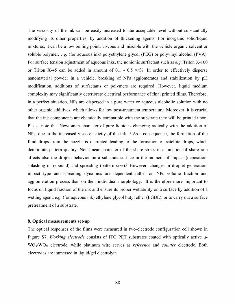
9. Definitions of parameters
Optical measurements are based on chronoabsorptometry (CA) technique which is a square-
wave potential step method coupled with optical spectroscopy used for analysis of switching
kinetics and contrast of the film. The EC testing was processed within an appropriate voltage
range (-2 V to 2 V), so as to avoid electrolyte oxidation and (eventual) ITO reduction. The main
output from CA measurements is the change in optical density ( ), which indicates how much ∆𝑂𝐷
the transmittance of the EC layer is reduced during the coloring process (or increased during
bleaching) for various levels of operational voltage. A linear stair pulse wave form shown in
Figure S10a was used to induce EC action, and the optical response recorded for = 800 nm was
analyzed according to Figure S10b.
The change in optical density is calculated using equation S2.
(S2)∆𝑂𝐷 = log10 ( 𝑇(𝑡𝑛,𝜆)
𝑇(𝑡𝑛 + 1,𝜆))where: and are transmittances of the films at λ = 800 nm before ( ) and after (𝑇(𝑡𝑛,𝜆) 𝑇(𝑡𝑛 + 1,𝜆) 𝑡𝑛,
) coloration process, respectively for each level of operational voltage (see also Figure 𝑡𝑛 + 1
S10b).
The impact of WOX NPs on reversibility of printed dual-phase EC films is measured as TSS
which represents so called site saturation effect.4 The TSS is defined according to equation S3 as
the difference in average transmittance ( , = 800 nm) of the film bleached by negative 𝑇(𝑡0,𝜆)
voltage to its bleached value after coloration for particular operating voltage (U) (see also Figure
S11). The TSS is equal to 0 for fully reversible optical effect.
(S3)∆𝑇𝑆𝑆 = 𝑇(𝑡0,𝜆) ‒ 𝑇(𝑡𝑚,𝜆, 𝑈)
Site saturation effect is quantified based on the CA results with linear stair pulse wave form
shown in Figure S10a used to induce EC action.
S13
Figure S10. Determination of as a function of operational voltage based on ∆𝑂𝐷
chronoabsorptometry technique in which a) linear stair pulse wave form is supplied to the film
and its b) optical response at = 800 nm is recorded showing change in transmittance depending
of the level of supplied voltage; an example shows optical response of a a-WO3/WOX film based
on a products of 4 hours long synthesis performed from the PTA precursor dissolved in 0.3 M
HCl (ortho-WO3·0.33H2O nanorods).

S14
Figure S11. Determination of as a function of operational voltage based on recorded optical ∆𝑇𝑆𝑆
response at = 800 nm; an example shows optical response of a-WO3 film with no NPs
incorporated.
Data obtained from CA measurements in which square wave potential (see Figure S12a) is
applied, enables estimation of the switching time for coloring and bleaching process according to
Figure S12b.
The coloration time (τcol) is defined as the time required for an EC device to change from its
bleached to colored state. In present studies the coloration time is defined as the requisite time
for reduction of the device’s transmittance to 80% of the final reduction according to equation S4
(see also Figure S12b).
(S4)𝜏𝑐𝑜𝑙 = 𝑓 ‒ 1(𝑇(𝑡2, 𝜆) + 0.2(𝑇(𝑡1, 𝜆) ‒ 𝑇(𝑡2, 𝜆))) ‒ 𝑡1
The bleaching time (τbl) is defined as the time required for an EC device to change from its
colored to bleached state. In these studies the bleaching time is defined as the requisite time for
change of the device’s transmittance to 80% of the final bleach level, according to equation S5
(see also Figure S12b).
(S5)𝜏𝑏𝑙 = 𝑓 ‒ 1(𝑇(𝑡'2, 𝜆) ‒ 0.2(𝑇(𝑡'2, 𝜆) ‒ 𝑇(𝑡'1, 𝜆))) ‒ 𝑡'1
The values of col and bl were determined as average values obtained from 5 consecutive cycles.

S15
Figure S12. Determination of coloration and bleaching time based on chronoabsorptometry
technique in which a) square wave form is supplied to the film and its b) optical response at =
800 nm is recorded showing change in transmittance; an example shows optical response of a a-
WO3/WOX film based on a products of 4 hours long synthesis performed from the PTA
precursor dissolved in 0.3 M HCl (ortho-WO3·0.33H2O nanorods).
10. Molecular crystal model
Molecular crystal models of monoclinic tungsten oxide (m-WO3) and orthorhombic tungsten
oxide hydrate (ortho-WO3·0.33H2O) were simulated using CrystalMaker® for Windows ver.
2.3.0. Crystal of m-WO3 presented in Figure S13a was simulated according to ICSD: 98-009-
1587 with following cell parameters and crystal structure (X, Y, Z): space group P 1 21/c 1;
space group number 14; a = 7.2973 Å; b = 7.5390 Å; c = 10.5150 Å; alpha = 90°; beta =
133.0250°; gamma = 90°; W1 = (0.03400, 0.47700, 0.28400); W2 = (0.52800, 0.03700, 0.28200);
O1 = (0.21400, 0.01300, 0.49300); O2 = (0.21600, 0.04300, 0.00800); O3 = (0.01900, 0.24100,
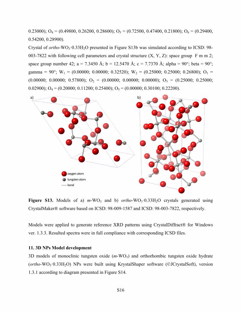
S16
0.23000); O4 = (0.49800, 0.26200, 0.28600); O5 = (0.72500, 0.47400, 0.21800); O6 = (0.29400,
0.54200, 0.28900).
Crystal of ortho-WO3·0.33H2O presented in Figure S13b was simulated according to ICSD: 98-
003-7822 with following cell parameters and crystal structure (X, Y, Z): space group F m m 2;
space group number 42; a = 7.3450 Å; b = 12.5470 Å; c = 7.7370 Å; alpha = 90°; beta = 90°;
gamma = 90°; W1 = (0.00000; 0.00000; 0.32520); W2 = (0.25000; 0.25000; 0.26800); O1 =
(0.00000; 0.00000; 0.57800); O2 = (0.00000; 0.00000; 0.00000); O3 = (0.25000; 0.25000;
0.02900); O4 = (0.20000; 0.11200; 0.25400); O5 = (0.00000; 0.30100; 0.22200).
Figure S13. Models of a) m-WO3 and b) ortho-WO3·0.33H2O crystals generated using
CrystalMaker® software based on ICSD: 98-009-1587 and ICSD: 98-003-7822, respectively.
Models were applied to generate reference XRD patterns using CrystalDiffract® for Windows
ver. 1.3.3. Resulted spectra were in full compliance with corresponding ICSD files.
11. 3D NPs Model development
3D models of monoclinic tungsten oxide (m-WO3) and orthorhombic tungsten oxide hydrate
(ortho-WO3·0.33H2O) NPs were built using KrystalShaper software (©JCrystalSoft), version
1.3.1 according to diagram presented in Figure S14.

S17
Figure S14. Schematic diagram of 3D NPs model creation process based on information
obtained from the analysis of preferential growth and SEM observations.
Quantitative information concerning the preferential crystalline orientation was obtained on a
basis of texture coefficient (TC) expressed by equation S65:
(S6)
𝑇𝐶(ℎ𝑘𝑙)𝑖 =
𝐼(ℎ𝑘𝑙)𝑖
𝐼0(ℎ𝑘𝑙)𝑖
1𝑁∑
𝑛
𝐼(ℎ𝑘𝑙)𝑛
𝐼0(ℎ𝑘𝑙)𝑛
where: is the observed intensity of plane, is the intensity of reflection 𝐼(ℎ𝑘𝑙)𝑖 (ℎ𝑘𝑙)𝑖 𝐼0(ℎ𝑘𝑙)𝑖 (ℎ𝑘𝑙)𝑖
of a polycrystalline sample, N is the total number of reflections taken into account, and (ℎ𝑘𝑙)
denotes the Miller indices of the lattice planes of a given signal. TC values larger than 1 indicate
a preferred orientation of the crystals/grains in the samples. By using this equation, the
preferential orientation of the facets can be understood. TC(hkl)i is expected to be unity for facets
which does not have preferential orientation. If TC(hkl)i is higher than unity, it is a preferentially
grown facet. TC(hkl)i values of facets of WOX NPs taken under account are presented in Figure
S15 and Figure S16.

S18
Figure S15. Texture coefficient spectra calculated for nanopowders obtained via hydrothermal
syntheses performed from non-acetified precursor solution after 2 h, 4 h and 6 h; Miller indices
of preferential orientations were highlighted by red color.
Figure S16. Texture coefficient spectra calculated for nanopowders obtained via hydrothermal
syntheses performed from precursor dissolved in a) 0.3 M HCl and b) 3 M HCl, after 2 h, 4 h and
6 h;

S19
An important input for 3D model creation of NPs, namely, shape, relative plane distances and
estimation of interplanar angles were obtained from SEM micrographs (see Figure S17 and
Figure 3 a - i in paper).
Figure S17. SEM image of a single ortho-WO3·0.33H2O NP obtained via hydrothermal
synthesis performed from precursor dissolved in 0.3 M HCl after 6 h; white lines were drawn
along the edges of the walls in order to estimate values of interplanar angles.
12. Fourier Transform Infrared Spectroscopy
The recorded FTIR spectra of obtained nanopowders presented in Figure S18 were studied in
order to identify coordinated water molecules in WO5(H2O) octahedron and vibrations in WO6
octahedron in accordance to the state of the art.6 The broad absorption band at 3470 cm-1 (-OH
stretching) and sharp band at 1610 cm-1 (-OH in plane bending) have been observed in the
powder synthesized from non-acetified precursor and precursor dissolved in 0.3 M HCl
indicating high amount of water molecules in the powder. No indicators of water have been
detected in the powder synthesized from the precursor dissolved in 3 M HCl indicating its
anhydrous nature. The same samples exhibit also strong absorption band at 970 cm-1 and 1000
cm-1 corresponding to the W-O stretching in WO6 octahedron. The broad band between 640 cm-1
and 955 cm-1 observed in all analyzed samples has been assigned to the W-O-W triplet
stretching.

S20
Figure S18. FTIR transmittance spectra of nanostructured products obtained from (I) non-
acetified precursor solution, (II) precursor dissolved in 0.3 M HCl and (III) precursor dissolved
in 3 M HCl after 6 h of hydrothermal synthesis.
13. Simultaneous Thermal Analysis (TGDSC)
Thermal analysis was performed in order to determine the coordinated water content in a
crystalline product of synthesis and to assess its thermal decomposition behavior.
The TG spectra presented in Figure S19 show distinct responses to increasing temperature in air
atmosphere. The total weight loss observed up to 600C for NPs produced from non-acetified
0.3 M HCl and 3 M HCl precursor was 2.37 wt% (m-WO3/ortho-WO3·0.33H2O), 4.1 wt%
(ortho-WO3·0.33H2O) and 0.5 wt% (m-WO3), respectively. The weight loss of ortho-
WO3·0.33H2O is almost double of theoretically calculated value of 2.58% for structurally
coordinated water. Higher value suggests the influence of physisorbed water on total weight loss,
which can be confirmed by weight loss observation even below 100 C.

S21
Figure S19. TG spectra of nanostructured products obtained from non-acetified precursor
solution, precursor dissolved in 0.3 M and precursor dissolved in 3 M HCl after 6 h of
hydrothermal synthesis.
The DSC curves (Figure S20) of NPs produced from non-acetified and 0.3 M HCl precursor
exhibit sharp exothermic peak at 315 and 325 C which correspond to removal of structurally
coordinated water and formation of crystalline WO3. No peaks were detected in DSC spectra of
the dehydrated m-WO3 synthesized from 3 M HCl precursor confirming the water absence
suggested by FTIR data.
Figure S20. DSC spectra of nanostructured products obtained from non-acetified precursor
solution, precursor dissolved in 0.3 M and precursor dissolved in 3 M HCl after 6 h of
hydrothermal synthesis.

S22
14. Model of agglomeration for various regular shaped NPs
An unfavorable aspect associated with nanostructured MOX is the particles agglomeration
leading to the formation of massive block, significantly reducing specific surface area. It is then
important to access thoroughly the influence of NPs agglomeration and NPs size distribution on
surface-to-volume ratio (SA:V). The simulated relations between SA:V and number of
agglomerated particles are presented in Figure S21, where NPs of a few various shapes are
described with simple assumption that the volume of all individual particles is equal. Particles
presented in such simulation have primary and regular shapes with unit volume. However, it is
very rare in practice to synthesize such ideal shaped nanostructures.
When considering the ideal dispersion of NPs in which agglomeration does not occur, nanoplates
and nanodiscs are the most preferable in terms of SA:V value. For agglomerated NPs, higher
values of SA:V are obtained for agglomerates of nanorods (agglomerates consisting of more than
3 NPs), although their individual specific surface area is not the highest among shapes under
consideration. The least favorable seem to be nanocubes in case of which SA:V is small for fine
dispersions and significantly drops down with increased number of agglomerated particles. As it
is very rare in practice to synthesize not agglomerated NPs, it is assumed that 1D nanorods are
the most desirable products of synthesis as long as their electrochemical application is
concerned. In contrast to the agglomerated NPs, hollow and hierarchical nanostructures
assembled in a highly periodic and porous manner generally exhibit much higher SA:V.11,12 The
van der Waals attraction between hierarchical structures is relatively weak due to larger size,
which makes them more advantageous in dispersions when comparing to anisotropic NPs.
However, the large size of such particles restricts their application in printable dispersions. The
synthesis of highly porous, hierarchical MOX nanostructures with sub-micrometer dimensions,
although very promising, is still a challenging issue.

S23
Figure S21. Model of agglomeration for various regular shaped NPs; the volume of all
individual particles is equal to 1; the term ‘ideal dispersion’ refers to the situation in which
agglomeration does not occur
15. Influence of the film thickness on electrochemical response
Influence of the film thickness on OD shown in Figure S22 was measured for films with similar
composition to the one reported in the present paper. In order to formulate an ink, 0.75 g of PTA
was dissolved in 7.5 g of aqueous isopropyl alcohol mixture with weight ratio of 70:30 and

S24
addition of oxalic acid in amount of 0.45 g. The solution was stirred for 15 minutes, 150 rpm at
60 C and filtered (Roth, 0.45 μm syringe filter). Individual layers (1 cm2) were printed 1, 3 and
5 times under equal environmental conditions on top of ITO PET substrate (Sigma-Aldrich, 1000
Å of ITO, 60 /sq, T > 75 % at 550 nm). All films were dried at room temperature for 24 h and
annealed in air at 120 C (EHRET, TK4067, Germany) for 1 h. Detailed information on device
encapsulation, experimental setup and measurements procedure can be found in our previous
paper concerning dual-phase inkjet printed films.13 Every successive printing pass causes the
layer grow of about 23 nm. Films printed 5 times exhibit change in optical density almost twice
higher than films printed with single pass.
Figure S22. Change in optical density in function of the a-WO3 film thickness. The EC action
was induced by applying voltage of ±4V.
16. Spectral response
Transmittance spectra for dual-phase films containing NPs synthesized in 6 h long process under
various precursor acidities in their colored and bleached states are illustrated in Figure S23. In
the bleached state all samples have high transmittances in a visible region indicating high
transparency of the coatings. Under application of a negative voltage (-2 V), all microstructures
exhibited observable transmittance modulation performance. The apparent transmittance
reduction of a-WO3/(m-WO3 + ortho-WO3·0.33H2O) at 525 nm comes from the existence of
both crystalline phases.

S25
Figure S23. UV-vis transmittance of dual-phase inkjet printed films containing NPs synthesized
in 6 h long process under various precursor acidities; bleaching and coloring optical states were
induced by 2 V operational voltages.
17. Graphics
Graphical processing of scientific recults concerning: graphical methods in measurments, photo
processing, vector image processing, arrangement of curvers and subfigures, and file formating
was performed according to video tutorials published in KEEP CALM and PUBLISH PAPERS
blog: http://www.keepcalmandpublishpapers.com
This source of knowledge contains a number of short (<15 min) video tutorials concerning
preparation of graphics for scientific communications. Each tutorial sets out a clear strategy to
assist students and researchers in creating effective visual graphics for journal submissions, grant
proposals, theses, posters and presentations. Each video tutorial is accompanied with written post
which gives an introduction to presented methods and techniques.
References
1. J. J. Cooper-White, J. E. Fagan, V. Tirtaatmadja, D. R. Lester, and D. V. Boger, J. Nonnewton. Fluid Mech., 2002, 106, 29–59.
2. R. J. Furbank and J. F. Morris, Phys. Fluids, 2004, 16, 1777.
3. T. R. Tuladhar and M. R. Mackley, J. Nonnewton. Fluid Mech., 2008, 148, 97–108.

S26
4. M. Denesuk and D. R. Uhlmann, J. Electrochem. Soc., 1996, 143, L186–L188.
5. S. Ruppi, Int. J. Refract. Met. Hard Mater., 2005, 23, 306–316.
6. J. Pfeifer, C. Guifang, P. Tekula-Buxbaum, B. A. Kiss, M. Frakas-Jahnke, and K. Vadasdi, J. Solid State Chem., 1995, 119, 90–97.
7. J. Jiang, Y. Li, J. Liu, X. Huang, C. Yuan, and X. W. D. Lou, Adv. Mater., 2012, 24, 5166–80.
8. P. M. Woodward, A. W. Sleight, and T. Vogt, J. Solid State Chem., 1997, 131, 9–17.
9. K. Yamanaka, H. Oakamoto, H. Kidou, and T. Kudo, Jpn. J. Appl. Phys., 1986, 25, 1420–1426.
10. M. Law, L. E. Greene, J. C. Johnson, R. Saykally, and P. Yang, Nat. Mater., 2005, 4, 455–9.
11. J.-H. Lee, Sensors Actuators B Chem., 2009, 140, 319–336.
12. Z. Gu, T. Zhai, B. Gao, X. Sheng, Y. Wang, and H. Fu, J. Phys. Chem. B, 2006, 110, 23829–23836.
13. P. J. Wojcik, A. S. Cruz, L. Santos, L. Pereira, R. Martins, and E. Fortunato, J. Mater. Chem., 2012, 22, 13268.