Embed Size (px)
Citation preview
440 Phys. Chem. Chem. Phys., 2013, 15, 440--443 This journal is c the Owner Societies 2013
Cite this: Phys. Chem. Chem. Phys.,2013, 15, 440
Nanoporous silicon networks as anodes for lithiumion batteries
Jia Zhu,wa Christopher Gladden,wa Nian Liu,b Yi Cuib and Xiang Zhang*a
Nanoporous silicon (Si) networks with controllable porosity and
thickness are fabricated by a simple and scalable electrochemical
process, and then released from Si wafers and transferred to
flexible and conductive substrates. These nanoporous Si networks
serve as high performance Li-ion battery electrodes, with an initial
discharge capacity of 2570 mA h g�1, above 1000 mA h g�1 after
200 cycles without any electrolyte additives.
Rechargeable lithium-ion batteries hold great promise asenergy storage devices to solve the temporal and geographicalmismatch between the supply and demand of electricity, andare therefore critical for many applications such as portableelectronics and electric vehicles. Electrodes in these batteriesare based on intercalation reactions in which Li+ ions areinserted (extracted) from an open host structure with electroninjection (removal).1–4 However, the current electrode materialshave limited specific charge storage capacity and cannotachieve the higher energy density, higher power density, andlonger lifespan that all these important applications require.3
Si as an alloying electrode material is attracting much attentionbecause it has the highest known theoretical charge capacity(4200 mA h g�1). However, it is challenging to overcome theissues associated with alloying and conversion reactions, whichinvolve large structure and volume changes (400% volumeexpansion for Si) during Li+ ion insertion and extraction. Theseissues can cause large hysteresis in the charge and dischargepotentials, low power rate, and short cycle life, due to materialinstability, and poor electron and ion conduction.5
Recently, Si nanostructures have been intensively exploredto attack the volume expansion and fracture problem.6–16 Forexample, many Si nanostructures, such as Si nanowires,6 carbon/Sispheres,9 Si nanotubes,17,18 core–shell crystalline/amorphous
Si nanowires,19 Si nanotubes, have also shown initial capacityclose to the theoretical limit, good (>90%) capacity retentionover a large number of cycles.20 However, low cost and fastthroughput processes with great mass and morphology controlare still desirable to reach the full potential for commercializa-tion. Here we developed a simple and scalable electrochemicalprocess to fabricate nanoporous Si networks with controllableporosity, which demonstrated a high initial discharge capacity of2570 mA h g�1 and 200 cycles in electrochemical tests. Even after200 cycles, this nanoporous Si network shows a capacity of above1000 mA h g�1. Good rate capability is demonstrated as well.
The nanoporous Si networks can be fabricated using a simpleand scalable process (Fig. 1). Silicon wafer chips (0.01–0.02 O cmp-type) are secured in a Teflon etch cell filled with a 1 : 3hydrofluoric acid and ethanol mixture. A nanoporous Si thin
Fig. 1 (a) Schematics of fabrication process flow. The nanoporous film is firstetched in 3 : 1 HF : EtOH under illumination, then undercut in 20 : 1 HF : EtOH.After being rinsed in EtOH it can be transferred to Cu foil and the substrate isreused. (b) Nanoporous Si film on a Si substrate. (c) Nanoporous Si filmtransferred to a Cu film.
a NSF Nano-scale Science and Engineering Center (NSEC), 3112 Etcheverry Hall,
University of California at Berkeley, Berkeley, California 94720, USA.
E-mail: [email protected] Department of Materials Science and Engineering, Stanford University, Stanford,
CA 94305, USA
† These authors contributed equally to this work.
Received 28th October 2012,Accepted 15th November 2012
DOI: 10.1039/c2cp44046f
www.rsc.org/pccp
PCCP
COMMUNICATION
Publ
ishe
d on
15
Nov
embe
r 20
12. D
ownl
oade
d by
Uni
vers
ity o
f C
alif
orni
a -
Ber
kele
y on
29/
06/2
015
18:4
0:13
.
View Article OnlineView Journal | View Issue
This journal is c the Owner Societies 2013 Phys. Chem. Chem. Phys., 2013, 15, 440--443 441
film is etched under constant current and light illumination. Sub-sequently the solution is exchanged for 1 : 20 HF : EtOH and etchedat 30 V to undercut the porous network and release it from thesilicon substrate.21 Finally the etch cell is flushed with pure ethanol,and then the thin layer of nanoporous Si is transferred to the Cu foilby slowly flowing ethanol over the chip while holding it in contactwith the foil. The porous layer on the Cu foil is then rinsed withhexane and allowed to air dry. The silicon substrate can be reusedmany times, ensuring efficient use of the Si source material.
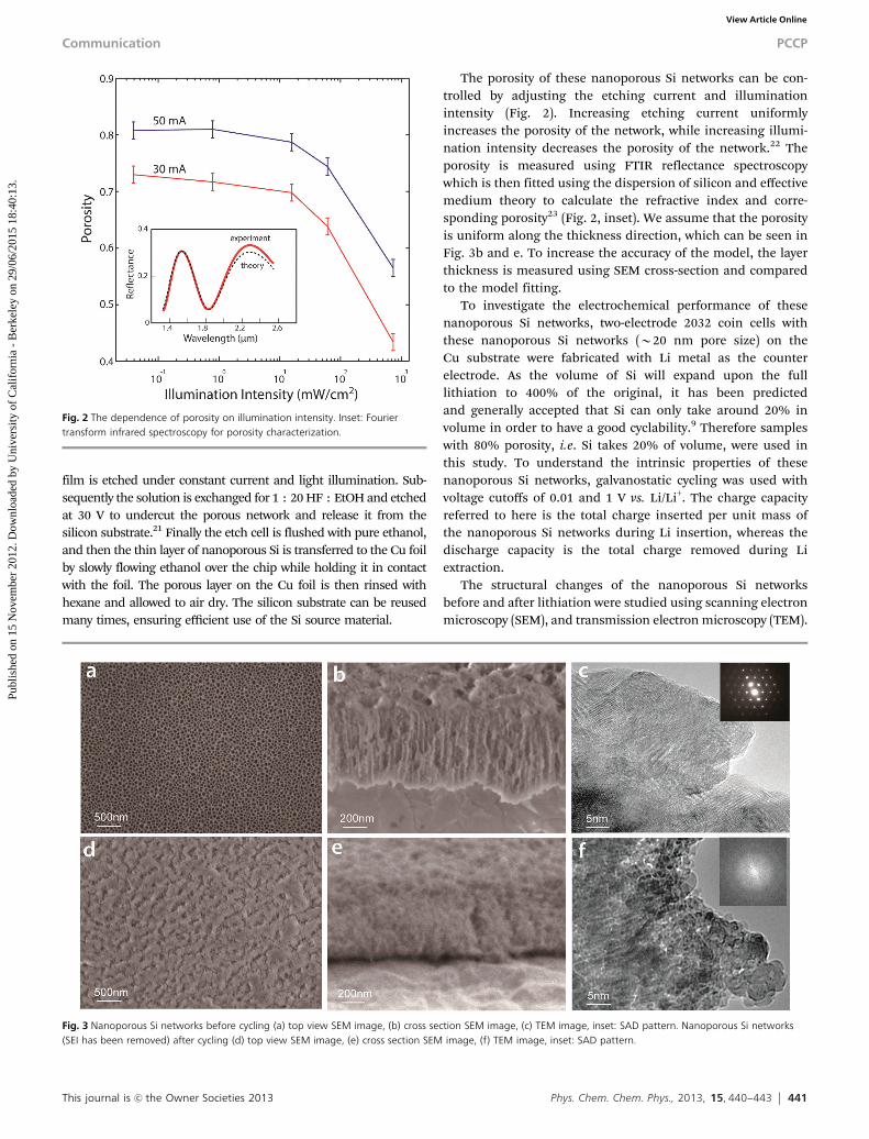
The porosity of these nanoporous Si networks can be con-trolled by adjusting the etching current and illuminationintensity (Fig. 2). Increasing etching current uniformlyincreases the porosity of the network, while increasing illumi-nation intensity decreases the porosity of the network.22 Theporosity is measured using FTIR reflectance spectroscopywhich is then fitted using the dispersion of silicon and effectivemedium theory to calculate the refractive index and corre-sponding porosity23 (Fig. 2, inset). We assume that the porosityis uniform along the thickness direction, which can be seen inFig. 3b and e. To increase the accuracy of the model, the layerthickness is measured using SEM cross-section and comparedto the model fitting.
To investigate the electrochemical performance of thesenanoporous Si networks, two-electrode 2032 coin cells withthese nanoporous Si networks (B20 nm pore size) on theCu substrate were fabricated with Li metal as the counterelectrode. As the volume of Si will expand upon the fulllithiation to 400% of the original, it has been predictedand generally accepted that Si can only take around 20% involume in order to have a good cyclability.9 Therefore sampleswith 80% porosity, i.e. Si takes 20% of volume, were used inthis study. To understand the intrinsic properties of thesenanoporous Si networks, galvanostatic cycling was used withvoltage cutoffs of 0.01 and 1 V vs. Li/Li+. The charge capacityreferred to here is the total charge inserted per unit mass ofthe nanoporous Si networks during Li insertion, whereas thedischarge capacity is the total charge removed during Liextraction.
The structural changes of the nanoporous Si networksbefore and after lithiation were studied using scanning electronmicroscopy (SEM), and transmission electron microscopy (TEM).
Fig. 2 The dependence of porosity on illumination intensity. Inset: Fouriertransform infrared spectroscopy for porosity characterization.
Fig. 3 Nanoporous Si networks before cycling (a) top view SEM image, (b) cross section SEM image, (c) TEM image, inset: SAD pattern. Nanoporous Si networks(SEI has been removed) after cycling (d) top view SEM image, (e) cross section SEM image, (f) TEM image, inset: SAD pattern.
Communication PCCP
Publ
ishe
d on
15
Nov
embe
r 20
12. D
ownl
oade
d by
Uni
vers
ity o
f C
alif
orni
a -
Ber
kele
y on
29/
06/2
015
18:4
0:13
. View Article Online
442 Phys. Chem. Chem. Phys., 2013, 15, 440--443 This journal is c the Owner Societies 2013
The as-fabricated nanoporous Si networks have an average poresize of 20 nm and 1 mm thickness as revealed in the SEM image(Fig. 3a). Cross-section SEM showed that the whole porous Sinetworks are in good contact with the Cu substrate (Fig. 3b),which is crucial for battery performance. The as-fabricatednanoporous Si networks were single crystalline, as confirmedby TEM (Fig. 3c). As shown in Fig. 3f, the nanoporous Sibecomes predominately amorphous during electrochemicalcycling, similar to what has been observed in SiNWs. SEM(Fig. 3e) studies found that the networks remained adheredto the substrate. The pore size of the networks also appearsto have decreased after lithiation, as expected from the pre-dicted volume change. It is important to note that the networksdo not pulverize after cycling because of the large porositywhich can accommodate the volume change, as shown inFig. 3d and e.
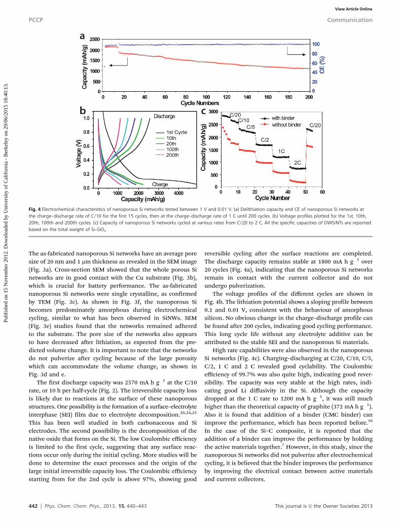
The first discharge capacity was 2570 mA h g�1 at the C/10rate, or 10 h per half-cycle (Fig. 2). The irreversible capacity lossis likely due to reactions at the surface of these nanoporousstructures. One possibility is the formation of a surface–electrolyteinterphase (SEI) film due to electrolyte decomposition.20,24,25
This has been well studied in both carbonaceous and Sielectrodes. The second possibility is the decomposition of thenative oxide that forms on the Si. The low Coulombic efficiencyis limited to the first cycle, suggesting that any surface reac-tions occur only during the initial cycling. More studies will bedone to determine the exact processes and the origin of thelarge initial irreversible capacity loss. The Coulombic efficiencystarting from for the 2nd cycle is above 97%, showing good
reversible cycling after the surface reactions are completed.The discharge capacity remains stable at 1800 mA h g�1 over20 cycles (Fig. 4a), indicating that the nanoporous Si networksremain in contact with the current collector and do notundergo pulverization.
The voltage profiles of the different cycles are shown inFig. 4b. The lithiation potential shows a sloping profile between0.1 and 0.01 V, consistent with the behaviour of amorphoussilicon. No obvious change in the charge–discharge profile canbe found after 200 cycles, indicating good cycling performance.This long cycle life without any electrolyte additive can beattributed to the stable SEI and the nanoporous Si materials.
High rate capabilities were also observed in the nanoporousSi networks (Fig. 4c). Charging–discharging at C/20, C/10, C/5,C/2, 1 C and 2 C revealed good cyclability. The Coulombicefficiency of 99.7% was also quite high, indicating good rever-sibility. The capacity was very stable at the high rates, indi-cating good Li diffusivity in the Si. Although the capacitydropped at the 1 C rate to 1200 mA h g�1, it was still muchhigher than the theoretical capacity of graphite (372 mA h g�1).Also it is found that addition of a binder (CMC binder) canimprove the performance, which has been reported before.16
In the case of the Si–C composite, it is reported that theaddition of a binder can improve the performance by holdingthe active materials together.7 However, in this study, since thenanoporous Si networks did not pulverize after electrochemicalcycling, it is believed that the binder improves the performanceby improving the electrical contact between active materialsand current collectors.
Fig. 4 Electrochemical characteristics of nanoporous Si networks tested between 1 V and 0.01 V. (a) Delithiation capacity and CE of nanoporous Si networks atthe charge–discharge rate of C/10 for the first 15 cycles, then at the charge–discharge rate of 1 C until 200 cycles. (b) Voltage profiles plotted for the 1st, 10th,20th, 100th and 200th cycles. (c) Capacity of nanoporous Si networks cycled at various rates from C/20 to 2 C. All the specific capacities of DWSiNTs are reportedbased on the total weight of Si–SiOx.
PCCP Communication
Publ
ishe
d on
15
Nov
embe
r 20
12. D
ownl
oade
d by
Uni
vers
ity o
f C
alif
orni
a -
Ber
kele
y on
29/
06/2
015
18:4
0:13
. View Article Online

This journal is c the Owner Societies 2013 Phys. Chem. Chem. Phys., 2013, 15, 440--443 443
Conclusion
In conclusion, we have shown that nanoporous Si networkanodes with 80% porosity have a high specific capacity(2570 mA h g�1) and good cycling performance (>200 cycles)without any electrolyte additives. Our nanoporous Si anodedesign is easy to fabricate and has good electronic contactbetween the network and the current collector. Thus, nano-porous Si networks can be a promising, higher-capacity alter-native for the existing graphite anode in Li ion batteries.
Acknowledgements
This work was supported by the U.S. Department of Energy, BasicEnergy Sciences Energy Frontier Research Center (DoE-LMI-EFRC)under award DOE DE-AC02-05CH11231.
Notes and references1 J. B. Goodenough and Y. Kim, Chem. Mater., 2009, 22, 587–603.2 M. S. Whittingham, ChemInform, 2004, 35, 4271.3 M. Armand and J. M. Tarascon, Nature, 2008, 451, 652–657.4 J. M. Tarascon and M. Armand, Nature, 2001, 414, 359–367.5 W.-J. Zhang, J. Power Sources, 2011, 196, 13–24.6 C. K. Chan, H. Peng, G. Liu, K. McIlwrath, X. F. Zhang, R. A. Huggins
and Y. Cui, Nat. Nanotechnol., 2008, 3, 31–35.7 A. Magasinski, P. Dixon, B. Hertzberg, A. Kvit, J. Ayala and
G. Yushin, Nat. Mater., 2010, 9, 353–358.8 N. Liu, H. Wu, M. T. McDowell, Y. Yao, C. Wang and Y. Cui, Nano
Lett., 2012, 12, 3315–3321.
9 S. D. Beattie, D. Larcher, M. Morcrette, B. Simon and J.-M. Tarascon,J. Electrochem. Soc., 2008, 155, A158–A163.
10 X.-W. Zhang, P. K. Patil, C. Wang, A. J. Appleby, F. E. Little andD. L. Cocke, J. Power Sources, 2004, 125, 206–213.
11 L. A. Riley, A. S. Cavanagh, S. M. George, Y. S. Jung, Y. Yan, S.-H. Leeand A. C. Dillon, ChemPhysChem, 2010, 11, 2124–2130.
12 M. Thakur, M. Isaacson, S. L. Sinsabaugh, M. S. Wong andS. L. Biswal, J. Power Sources, 2012, 205, 426–432.
13 Y. Zhao, X. Liu, H. Li, T. Zhai and H. Zhou, Chem. Commun., 2012,48, 5079–5081.
14 M. Ge, J. Rong, X. Fang and C. Zhou, Nano Lett., 2012, 12, 2318–2323.15 I. Kovalenko, B. Zdyrko, A. Magasinski, B. Hertzberg, Z. Milicev,
R. Burtovyy, I. Luzinov and G. Yushin, Science, 2011, 334, 75–79.16 D. Mazouzi, B. Lestriez, L. Roue and D. Guyomard, Electrochem.
Solid-State Lett., 2009, 12, A215–A218.17 T. Song, J. Xia, J.-H. Lee, D. H. Lee, M.-S. Kwon, J.-M. Choi, J. Wu,
S. K. Doo, H. Chang, W. I. Park, D. S. Zang, H. Kim, Y. Huang,K.-C. Hwang, J. A. Rogers and U. Paik, Nano Lett., 2010, 10, 1710–1716.
18 M.-H. Park, M. G. Kim, J. Joo, K. Kim, J. Kim, S. Ahn, Y. Cui andJ. Cho, Nano Lett., 2009, 9, 3844–3847.
19 L.-F. Cui, R. Ruffo, C. K. Chan, H. Peng and Y. Cui, Nano Lett., 2008,9, 491–495.
20 H. Wu, G. Chan, J. W. Choi, I. Ryu, Y. Yao, M. T. McDowell,S. W. Lee, A. Jackson, Y. Yang, L. Hu and Y. Cui, Nat. Nanotechnol.,2012, 7, 310–315.
21 Y. Kanemitsu, H. Uto, Y. Masumoto, T. Matsumoto, T. Futagi andH. Mimura, Phys. Rev. B: Condens. Matter Mater. Phys., 1993, 48,2827–2830.
22 C. Levy-Clement, A. Lagoubi, R. Tenne and M. Neumann-Spallart,Electrochim. Acta, 1992, 37, 877–888.
23 K. Vanga, D. Cheam, C. Middlebrook and P. Bergstrom, Phys. StatusSolidi C, 2011, 8, 1941–1945.
24 D. Aurbach, J. Power Sources, 2000, 89, 206–218.25 P. Verma, P. Maire and P. Novak, Electrochim. Acta, 2010, 55,
6332–6341.
Communication PCCP
Publ
ishe
d on
15
Nov
embe
r 20
12. D
ownl
oade
d by
Uni
vers
ity o
f C
alif
orni
a -
Ber
kele
y on
29/
06/2
015
18:4
0:13
. View Article Online