Embed Size (px)
Citation preview
Rose-Hulman Institute of Technology
Authors: Elena Chong Loo
Lingtongyue Jin
ECE310: Final Laboratory Report
“Infrared Digital Communication System”
Submitted to: Professor Yong Jin Kim
Submission Date: October 13th, 2014
Fall 2014
Infrared Digital Communication System
1
Executive Summary
The goal of the first five weeks of laboratory for the ECE310 course was to build an infrared digital
communication system from scratch capable of transmitting and receiving data produced by a
pseudorandom data generator. This provided the students a better understanding of how each
subsystems are used together to allow an efficient communication of information.
This digital communication system was completed successfully by the authors. The verification of
the system was done using the equipment in lab B200 bench 4. The breadboard, including all the
electronic components were bought in the school part room. The functionality of the transmitter
and receiver were verified by sending the pseudorandom data from the transmitter and receiving
the same signal in the receiver sider. The verification was done using an oscilloscope by visualizing
the pseudorandom data at the transmitter and the receiver. Both devices were placed at 45 inches
away, which was the maximum spacing over which the circuit continues to operate properly.
Infrared Digital Communication System
2
1. Introduction
1.1 Project Overview
This project was developed through the laboratory requirement of the ECE310 course. The
infrared digital communication system, which consists of a transmitter and a receiver circuit
was built by the authors throughout the first five weeks of required laboratory. Two
breadboards and electronics components, such as resistors, capacitors, op amps, etc., were
bought from the part room at the school and used as part of the circuit. The main purpose of
the laboratories were to provide the students a better understanding of how each subsystem of
the digital communication system, such as the comparator, sampler, modulator, filters works.
During every laboratory session, the authors designed, built, and verified the functionality of
each stage using the equipment from B200 lab. Datasheets were also used to check the pin out
of each chip used in the design part of the lab. As the project progressed, a schematic diagram
were made for each components using PSpice OrCAD Capture. Also, two PIC16F690 chips
were used in this lab. The provided code was programmed into the PIC using the MPLAB IDE
software available free from Microchip.
1.2 Accomplishments
Table 1 describes the accomplishment of each of the first five laboratory done for this course.
The lab manual provided to the authors at the beginning of the course were used as a reference
for the description of the laboratory projects.
Laboratory Projects Description
Interfacing to Infrared Transducers Understand the functionality of an LED
and phototransistor. Design and build a
trans-impedance amplifier for the
phototransistor.
Digital In – Digital Out Construction of a pseudorandom data
generator, a threshold comparator, and a
sampling circuit.
Infrared Digital Communication System
3
Modulation and Receiver Front End Design and characterization of an active
band-pass receiver filter. Design of a
carrier oscillator and a modulator to
provide on-off keying of the transmitter.
Envelope Detector Design and characterization of an envelope
detector. End-to-end checkout of the
infrared digital communication system.
Clock Recovery Design, construction, test, and
characterization of a clock recovery circuit
using a microcontroller.
Table 1. Description of laboratory projects.
2. Circuit Documentation
2.1 Description of the Infrared Digital Communication System Design
A circuit for the transmitter and receiver were built separately on two breadboards. The design
of each part will be described in detail. First, the design of the transmitter will be discussed,
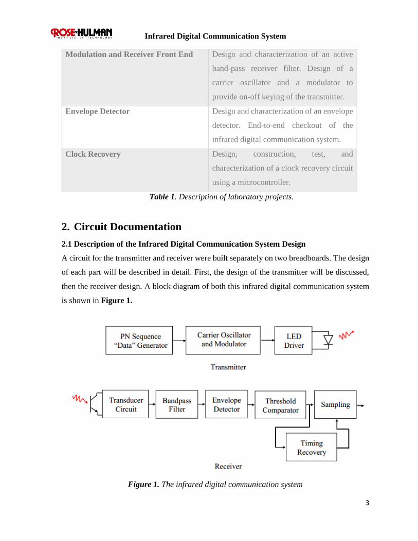
then the receiver design. A block diagram of both this infrared digital communication system
is shown in Figure 1.
Figure 1. The infrared digital communication system
Infrared Digital Communication System
4
2.2 Transmitter Circuit Design
The transmitter board consists of three main subsystems, a pseudorandom “data” generator,
a carrier oscillator and modulator, and an infrared LED, as shown in the block diagram of
the transmitter in Figure 1.
1. A pseudorandom sequence generator (PSG), in this case, a 16-bit shift register that
cycles through all 15 non-zero states, was built using the PIC16F690 microprocessor
to simulate “data” to transmit over the channel. The design of the PSG was
implemented by programming the provided code into the PIC microcontroller. Another
way to do this process would have been using discrete gates. The code for the PIC is
attached in the Appendix. The clock frequency, called the “bit clock”, was set at 100Hz
square wave using the function generator Tektronix AFG 3022B. This is the external
clock input produced to synchronize the pseudorandom sequence output.
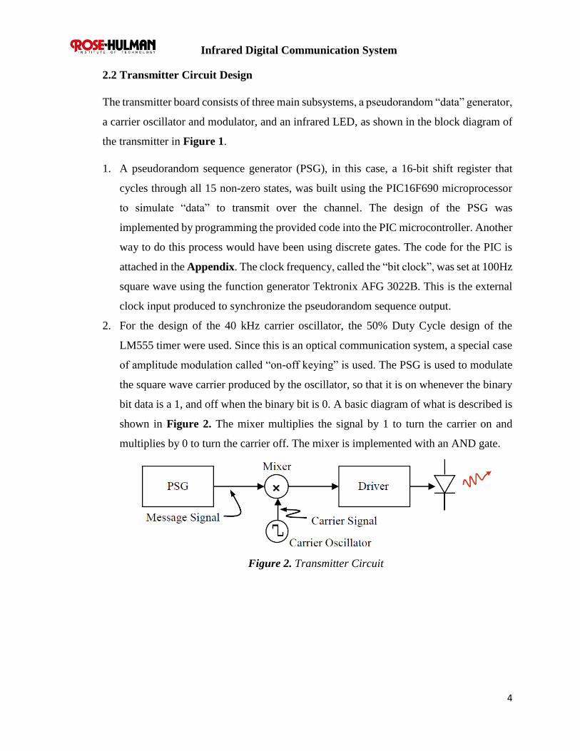
2. For the design of the 40 kHz carrier oscillator, the 50% Duty Cycle design of the
LM555 timer were used. Since this is an optical communication system, a special case
of amplitude modulation called “on-off keying” is used. The PSG is used to modulate
the square wave carrier produced by the oscillator, so that it is on whenever the binary
bit data is a 1, and off when the binary bit is 0. A basic diagram of what is described is
shown in Figure 2. The mixer multiplies the signal by 1 to turn the carrier on and
multiplies by 0 to turn the carrier off. The mixer is implemented with an AND gate.
Figure 2. Transmitter Circuit
Infrared Digital Communication System
5
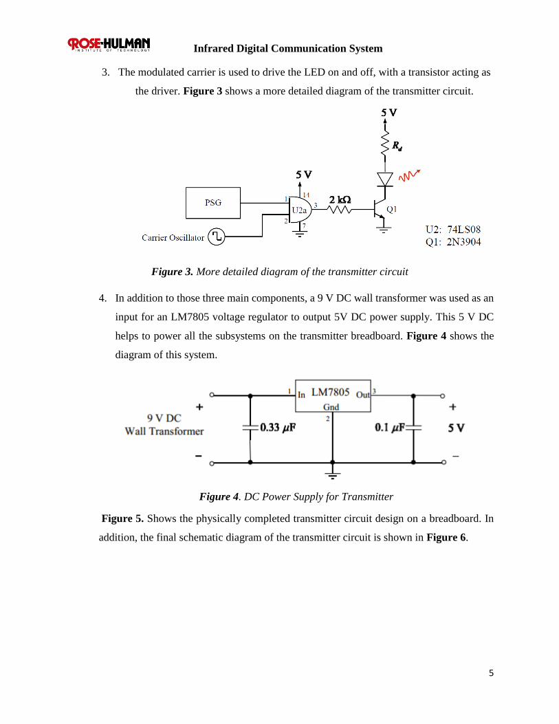
3. The modulated carrier is used to drive the LED on and off, with a transistor acting as
the driver. Figure 3 shows a more detailed diagram of the transmitter circuit.
Figure 3. More detailed diagram of the transmitter circuit
4. In addition to those three main components, a 9 V DC wall transformer was used as an
input for an LM7805 voltage regulator to output 5V DC power supply. This 5 V DC
helps to power all the subsystems on the transmitter breadboard. Figure 4 shows the
diagram of this system.
Figure 4. DC Power Supply for Transmitter
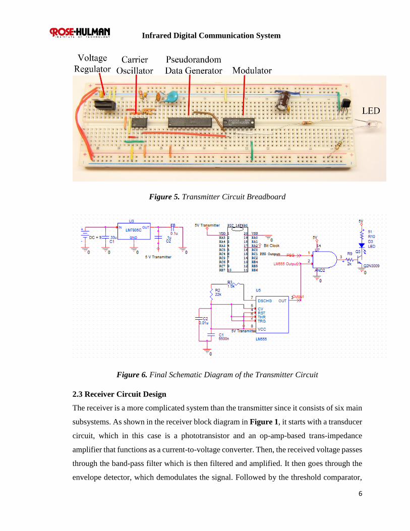
Figure 5. Shows the physically completed transmitter circuit design on a breadboard. In
addition, the final schematic diagram of the transmitter circuit is shown in Figure 6.
Infrared Digital Communication System
6
Figure 5. Transmitter Circuit Breadboard
Figure 6. Final Schematic Diagram of the Transmitter Circuit
2.3 Receiver Circuit Design
The receiver is a more complicated system than the transmitter since it consists of six main
subsystems. As shown in the receiver block diagram in Figure 1, it starts with a transducer
circuit, which in this case is a phototransistor and an op-amp-based trans-impedance
amplifier that functions as a current-to-voltage converter. Then, the received voltage passes
through the band-pass filter which is then filtered and amplified. It then goes through the
envelope detector, which demodulates the signal. Followed by the threshold comparator,
Infrared Digital Communication System
7
an LM311 configured to produce logic-compatible output voltage levels. The sampling
circuit is a D flip-flop. Finally the clock for the flip-flop must be recovered from the
received data stream.
1. The infrared transducer in the receiver circuit is a phototransistor, which is basically a
BJT transistor with special base configuration together with an op-amp trans-
impedance amplifier, which convert current to voltage.
2. An LM311 is used as a voltage comparator. The binary data received that go through
the demodulator will be distorted and noisy, and the voltage levels will not be standard
logic levels. Thus, the voltage comparator is used to recover the standard voltage levels.
3. The 74LS74A D flip-flop is used to sample the signal. Since the D flip-flop is rising-
edge triggered and the PSG is falling-edge triggered, this allows the received signal
time to go through the receiver filters and also better timing for sampling.
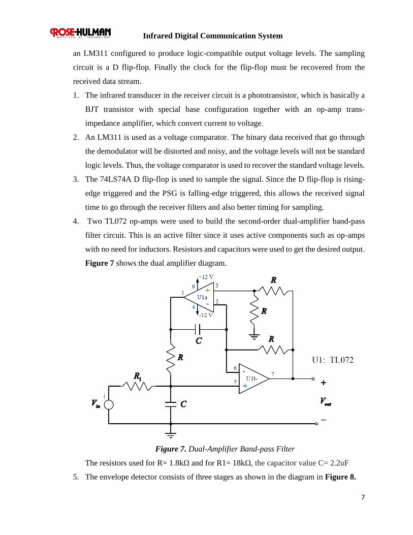
4. Two TL072 op-amps were used to build the second-order dual-amplifier band-pass
filter circuit. This is an active filter since it uses active components such as op-amps
with no need for inductors. Resistors and capacitors were used to get the desired output.
Figure 7 shows the dual amplifier diagram.
Figure 7. Dual-Amplifier Band-pass Filter
The resistors used for R= 1.8kΩ and for R1= 18kΩ, the capacitor value C= 2.2uF
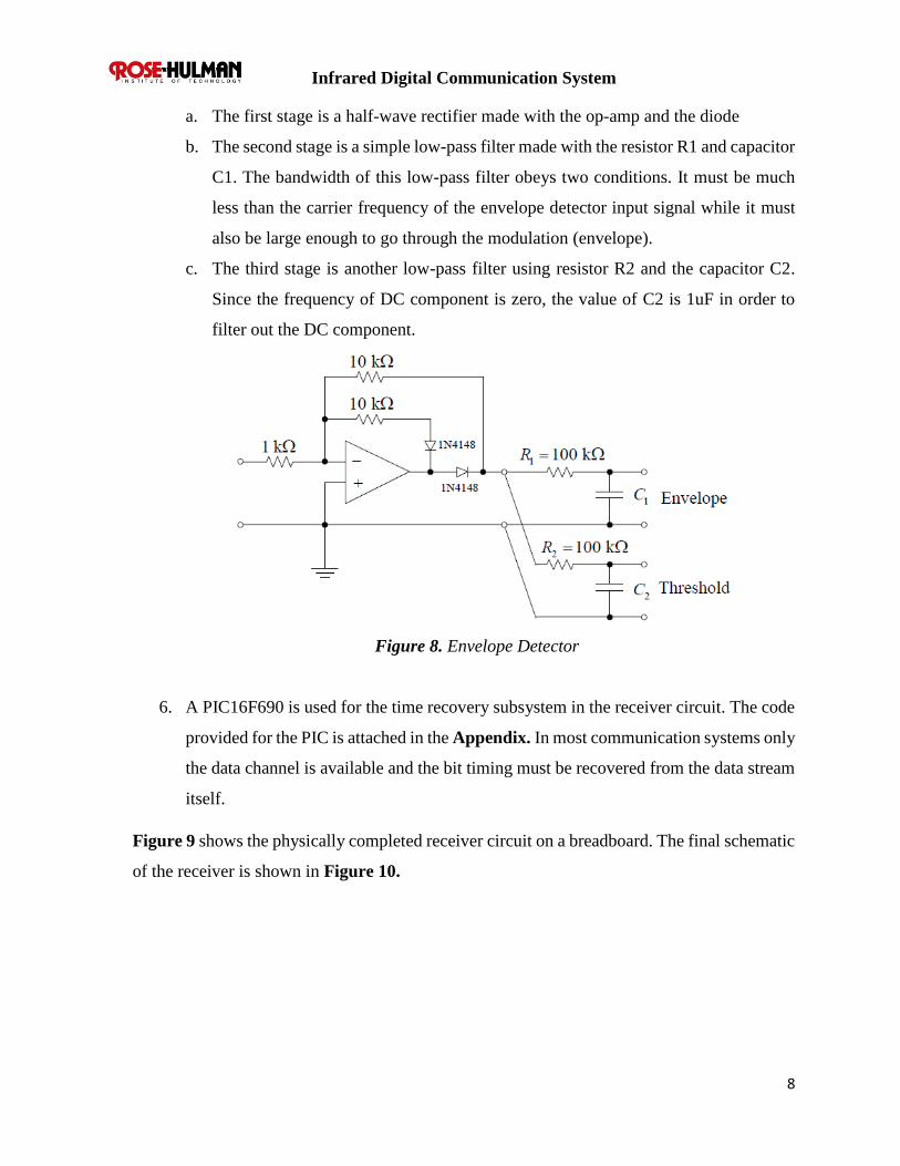
5. The envelope detector consists of three stages as shown in the diagram in Figure 8.
Infrared Digital Communication System
8
a. The first stage is a half-wave rectifier made with the op-amp and the diode
b. The second stage is a simple low-pass filter made with the resistor R1 and capacitor
C1. The bandwidth of this low-pass filter obeys two conditions. It must be much
less than the carrier frequency of the envelope detector input signal while it must
also be large enough to go through the modulation (envelope).
c. The third stage is another low-pass filter using resistor R2 and the capacitor C2.
Since the frequency of DC component is zero, the value of C2 is 1uF in order to
filter out the DC component.
Figure 8. Envelope Detector
6. A PIC16F690 is used for the time recovery subsystem in the receiver circuit. The code
provided for the PIC is attached in the Appendix. In most communication systems only
the data channel is available and the bit timing must be recovered from the data stream
itself.
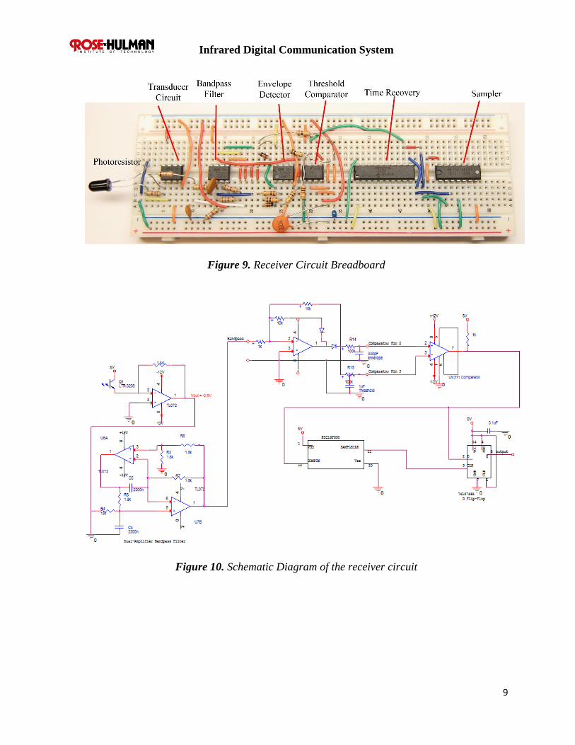
Figure 9 shows the physically completed receiver circuit on a breadboard. The final schematic
of the receiver is shown in Figure 10.
Infrared Digital Communication System
9
Figure 9. Receiver Circuit Breadboard
Figure 10. Schematic Diagram of the receiver circuit
Infrared Digital Communication System
10
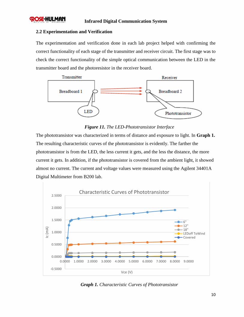
2.2 Experimentation and Verification
The experimentation and verification done in each lab project helped with confirming the
correct functionality of each stage of the transmitter and receiver circuit. The first stage was to
check the correct functionality of the simple optical communication between the LED in the
transmitter board and the photoresistor in the receiver board.
Figure 11. The LED-Phototransistor Interface
The phototransistor was characterized in terms of distance and exposure to light. In Graph 1.
The resulting characteristic curves of the phototransistor is evidently. The farther the
phototransistor is from the LED, the less current it gets, and the less the distance, the more
current it gets. In addition, if the phototransistor is covered from the ambient light, it showed
almost no current. The current and voltage values were measured using the Agilent 34401A
Digital Multimeter from B200 lab.
Graph 1. Characteristic Curves of Phototransistor
-0.5000
0.0000
0.5000
1.0000
1.5000
2.0000
2.5000
0.0000 1.0000 2.0000 3.0000 4.0000 5.0000 6.0000 7.0000 8.0000 9.0000
Ic (
mA
)
Vce (V)
Characteristic Curves of Phototransistor
6"12"18"LEDoff ToWindCovered
Infrared Digital Communication System
11
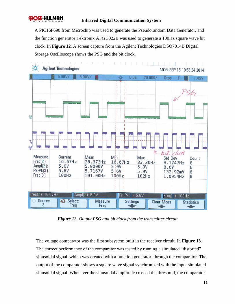
A PIC16F690 from Microchip was used to generate the Pseudorandom Data Generator, and
the function generator Tektronix AFG 3022B was used to generate a 100Hz square wave bit
clock. In Figure 12. A screen capture from the Agilent Technologies DSO7014B Digital
Storage Oscilloscope shows the PSG and the bit clock.
Figure 12. Output PSG and bit clock from the transmitter circuit
The voltage comparator was the first subsystem built in the receiver circuit. In Figure 13.
The correct performance of the comparator was tested by running a simulated “distorted”
sinusoidal signal, which was created with a function generator, through the comparator. The
output of the comparator shows a square wave signal synchronized with the input simulated
sinusoidal signal. Whenever the sinusoidal amplitude crossed the threshold, the comparator
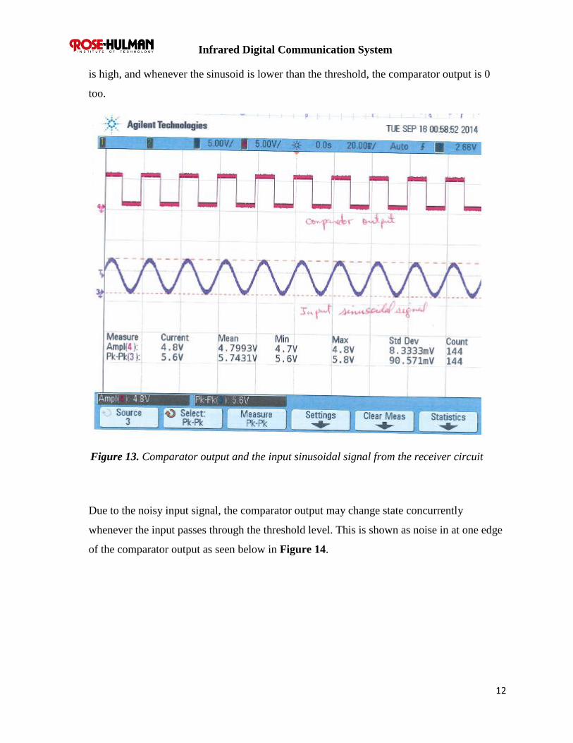
Infrared Digital Communication System
12
is high, and whenever the sinusoid is lower than the threshold, the comparator output is 0
too.
Figure 13. Comparator output and the input sinusoidal signal from the receiver circuit
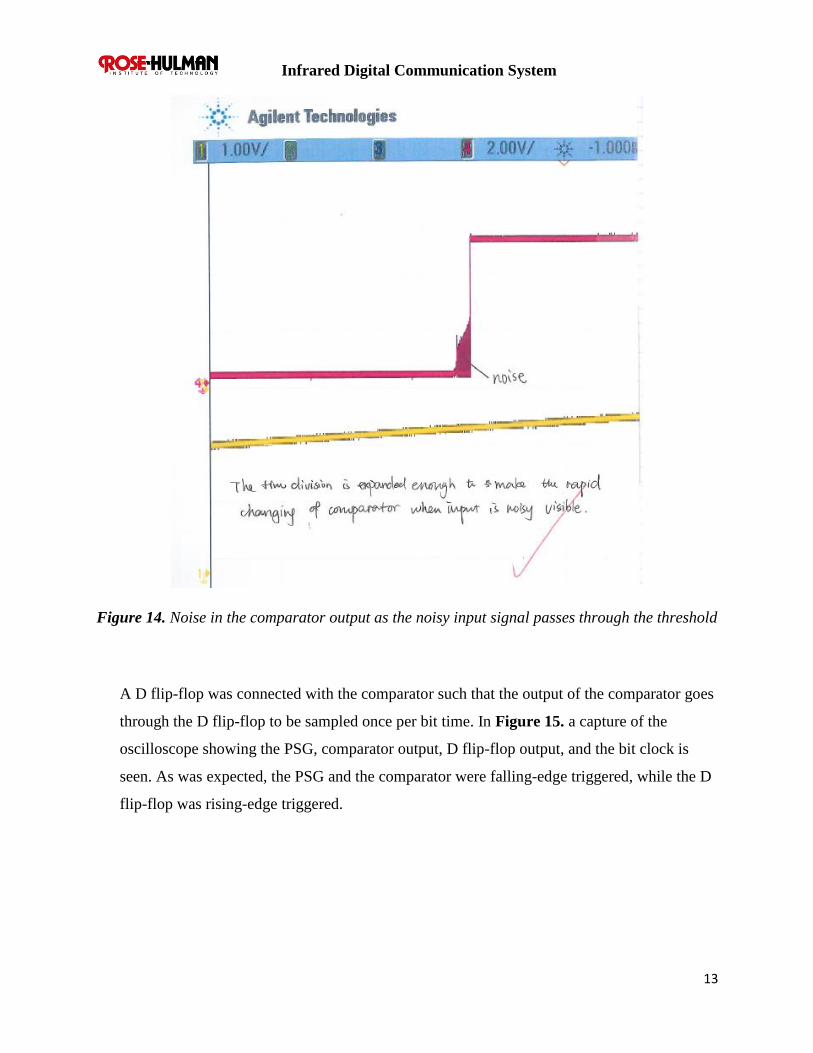
Due to the noisy input signal, the comparator output may change state concurrently
whenever the input passes through the threshold level. This is shown as noise in at one edge
of the comparator output as seen below in Figure 14.
Infrared Digital Communication System
13
Figure 14. Noise in the comparator output as the noisy input signal passes through the threshold
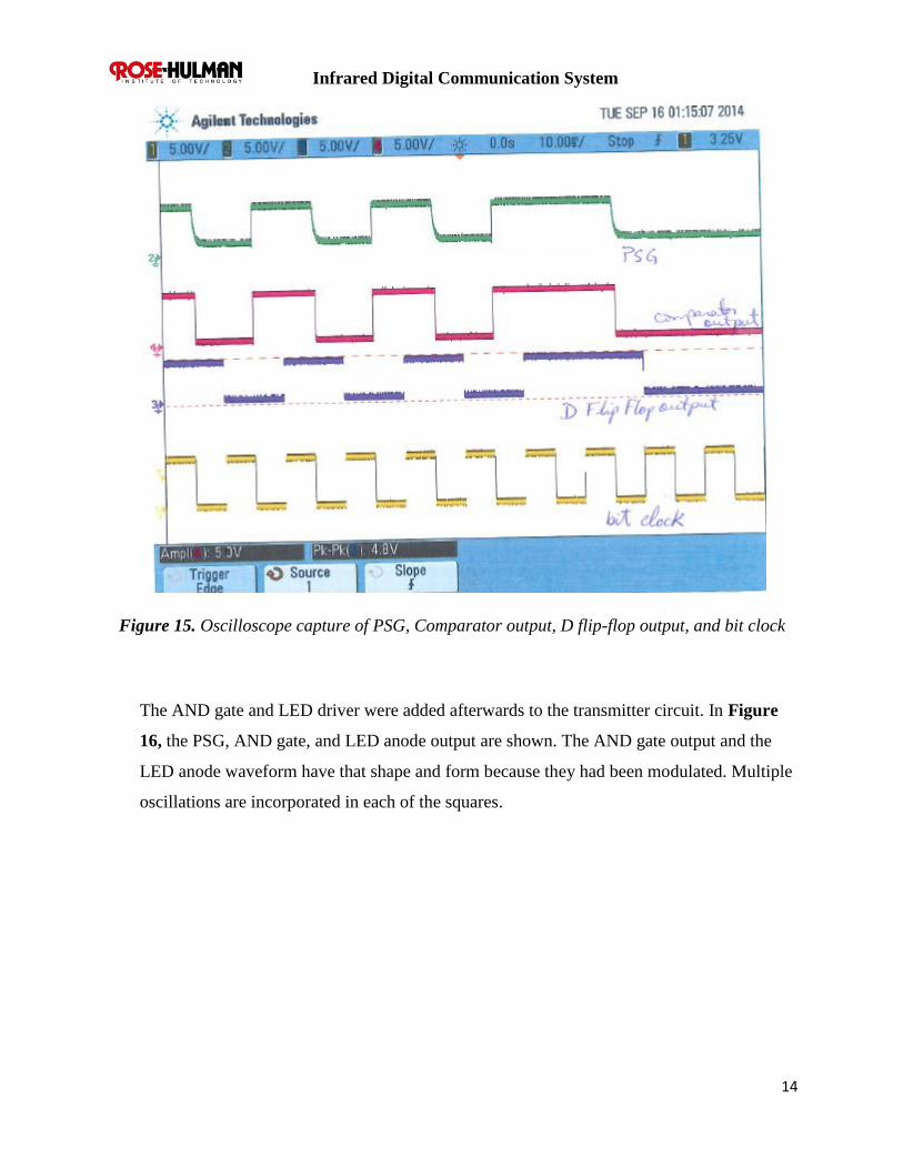
A D flip-flop was connected with the comparator such that the output of the comparator goes
through the D flip-flop to be sampled once per bit time. In Figure 15. a capture of the
oscilloscope showing the PSG, comparator output, D flip-flop output, and the bit clock is
seen. As was expected, the PSG and the comparator were falling-edge triggered, while the D
flip-flop was rising-edge triggered.
Infrared Digital Communication System
14
Figure 15. Oscilloscope capture of PSG, Comparator output, D flip-flop output, and bit clock
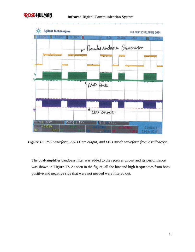
The AND gate and LED driver were added afterwards to the transmitter circuit. In Figure
16, the PSG, AND gate, and LED anode output are shown. The AND gate output and the
LED anode waveform have that shape and form because they had been modulated. Multiple
oscillations are incorporated in each of the squares.
Infrared Digital Communication System
15
Figure 16. PSG waveform, AND Gate output, and LED anode waveform from oscilloscope
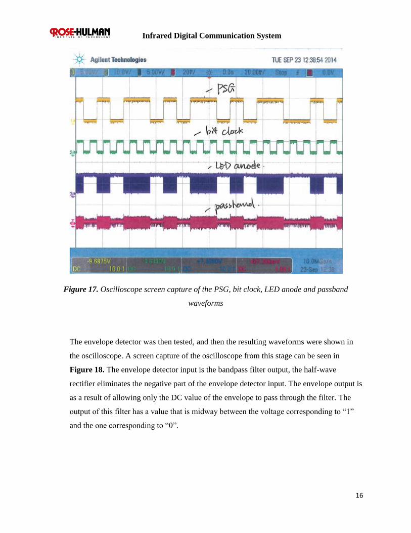
The dual-amplifier bandpass filter was added to the receiver circuit and its performance
was shown in Figure 17. As seen in the figure, all the low and high frequencies from both
positive and negative side that were not needed were filtered out.
Infrared Digital Communication System
16
Figure 17. Oscilloscope screen capture of the PSG, bit clock, LED anode and passband
waveforms
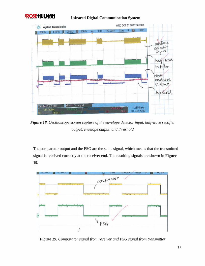
The envelope detector was then tested, and then the resulting waveforms were shown in
the oscilloscope. A screen capture of the oscilloscope from this stage can be seen in
Figure 18. The envelope detector input is the bandpass filter output, the half-wave
rectifier eliminates the negative part of the envelope detector input. The envelope output is
as a result of allowing only the DC value of the envelope to pass through the filter. The
output of this filter has a value that is midway between the voltage corresponding to “1”
and the one corresponding to “0”.
Infrared Digital Communication System
17
Figure 18. Oscilloscope screen capture of the envelope detector input, half-wave rectifier
output, envelope output, and threshold
The comparator output and the PSG are the same signal, which means that the transmitted
signal is received correctly at the receiver end. The resulting signals are shown in Figure
19.
Figure 19. Comparator signal from receiver and PSG signal from transmitter
Infrared Digital Communication System
18
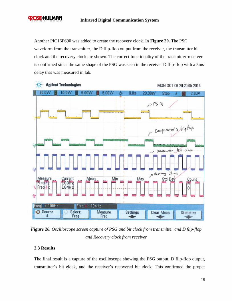
Another PIC16F690 was added to create the recovery clock. In Figure 20. The PSG
waveform from the transmitter, the D flip-flop output from the receiver, the transmitter bit
clock and the recovery clock are shown. The correct functionality of the transmitter-receiver
is confirmed since the same shape of the PSG was seen in the receiver D flip-flop with a 5ms
delay that was measured in lab.
Figure 20. Oscilloscope screen capture of PSG and bit clock from transmitter and D flip-flop
and Recovery clock from receiver
2.3 Results
The final result is a capture of the oscilloscope showing the PSG output, D flip-flop output,
transmitter’s bit clock, and the receiver’s recovered bit clock. This confirmed the proper

Infrared Digital Communication System
19
operation of both final transmitter and receiver circuit since the D flip-flop output is the same
signal as the PSG but with a delay which was measured in the lab to be 5ms. Figure 20 shows
the screen capture from the oscilloscope.
In addition, 42.5 ~ 44.5 inches was the maximum spacing between the transmitter and receiver
where a signal can still be seen in the oscilloscope.
Infrared Digital Communication System
20
3. Conclusion
Throughout the course of five weeks, the authors were able to design and build an optical
digital communication system involving a transmitter-receiver circuit. The fully operation of
the transmitter and receiver were verified at the end of the fifth laboratory project.
The authors were able to learn what is involved in designing and building a digital
communication system.
Infrared Digital Communication System
21
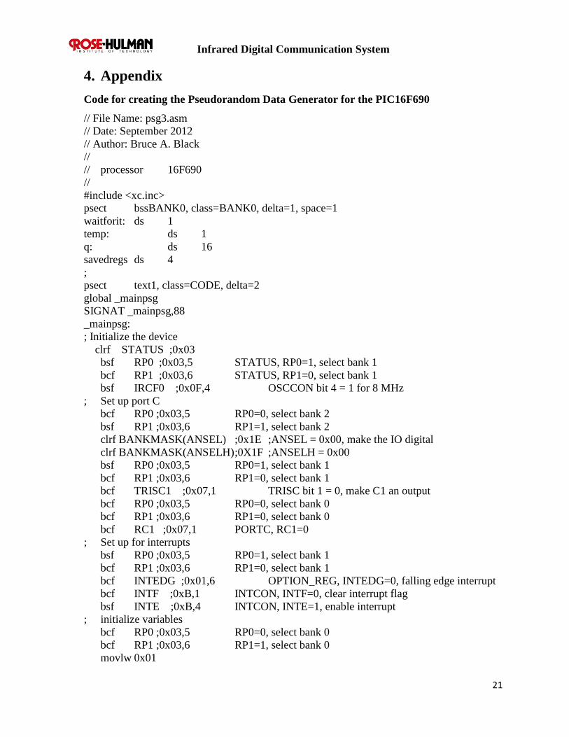
4. Appendix
Code for creating the Pseudorandom Data Generator for the PIC16F690
// File Name: psg3.asm
// Date: September 2012
// Author: Bruce A. Black
//
// processor 16F690
//
#include <xc.inc>
psect bssBANK0, class=BANK0, delta=1, space=1
waitforit: ds 1
temp: ds 1
q: ds 16
savedregs ds 4
;
psect text1, class=CODE, delta=2
global _mainpsg
SIGNAT _mainpsg,88
_mainpsg:
; Initialize the device
clrf STATUS ;0x03
bsf RP0 ;0x03,5 STATUS, RP0=1, select bank 1
bcf RP1 ;0x03,6 STATUS, RP1=0, select bank 1
bsf IRCF0 ;0x0F,4 OSCCON bit 4 = 1 for 8 MHz
; Set up port C
bcf RP0 ;0x03,5 RP0=0, select bank 2
bsf RP1 ;0x03,6 RP1=1, select bank 2
clrf BANKMASK(ANSEL) ;0x1E ;ANSEL = 0x00, make the IO digital
clrf BANKMASK(ANSELH) ;0X1F ;ANSELH = 0x00
bsf RP0 ;0x03,5 RP0=1, select bank 1
bcf RP1 ;0x03,6 RP1=0, select bank 1
bcf TRISC1 ;0x07,1 TRISC bit 1 = 0, make C1 an output
bcf RP0 ;0x03,5 RP0=0, select bank 0
bcf RP1 ;0x03,6 RP1=0, select bank 0
bcf RC1 ;0x07,1 PORTC, RC1=0
; Set up for interrupts
bsf RP0 ;0x03,5 RP0=1, select bank 1
bcf RP1 ;0x03,6 RP1=0, select bank 1
bcf INTEDG ;0x01,6 OPTION_REG, INTEDG=0, falling edge interrupt
bcf INTF ;0xB,1 INTCON, INTF=0, clear interrupt flag
bsf INTE ;0xB,4 INTCON, INTE=1, enable interrupt
; initialize variables
bcf RP0 ;0x03,5 RP0=0, select bank 0
bcf RP1 ;0x03,6 RP1=1, select bank 0
movlw 0x01
Infrared Digital Communication System
22
movwf (q)
movlw 0x00
movwf (q+1)
movwf (q+2)
movwf (q+3)
movwf (q+4)
movwf (q+5)
movwf (q+6)
movwf (q+7)
movwf (q+8)
movwf (q+9)
movwf (q+10)
movwf (q+11)
movwf (q+12)
movwf (q+13)
movwf (q+14)
movwf (q+15)
; enable interrupt
bsf GIE ;0x0B,7 INTCON, GIE=1
; This is the main loop
there: movlw 0x01
movwf (waitforit) ;Set waitforit=1
; wait here for an interrupt
here: movf (waitforit),f
btfss ZERO ;0x03,2 STATUS, Z, Exit loop if waitforit=0
goto here
; advance the pseudorandom sequence
movf (q+0),w
movwf (temp)
movf (q+1),w
movwf (q)
xorwf (temp),f
movf (q+2),w
movwf (q+1)
movf (q+3),w
movwf (q+2)
xorwf (temp),f
movf (q+4),w
movwf (q+3)
movf (q+5),w
movwf (q+4)
movf (q+6),w
movwf (q+5)
movf (q+7),w
movwf (q+6)
movf (q+8),w
Infrared Digital Communication System
23
movwf (q+7)
movf (q+9),w
movwf (q+8)
movf (q+10),w
movwf (q+9)
movf (q+11),w
movwf (q+10)
movf (q+12),w
movwf (q+11)
xorwf (temp),f
movf (q+13),w
movwf (q+12)
movf (q+14),w
movwf (q+13)
movf (q+15),w
movwf (q+14)
movf (temp),w
movwf (q+15)
; update the output
movf (q),f ;Test q(0) for zero
btfss ZERO ;0x03,2 STATUS, Z
goto setone
setzro: bcf RC1 ;0x07,1 RC1=0
goto there ;Go back to top of loop
setone: bsf RC1 ;0x07,1 RC1=1
goto there ;Go back to top of loop
; The interrupt routine
psect intentry, class=CODE, delta=2
interrupt_function:
bcf RP0 ;0x03,5 RP0=0, select bank 0
bcf RP1 ;0x03,6 RP1=0, select bank 0
movwf (savedregs)
movf STATUS, w ;0x03,w save STATUS
movwf (savedregs+1)
movf FSR, w ;0x04,w save FSR
movwf (savedregs+2)
movf PCLATH, w ;0x0A,w save PCLATH
movwf (savedregs+3)
ljmp clockedge
;
psect text2, class=CODE, delta=2
clockedge:
btfss INTE ;0xB,4 INTCON, INTE=1?
goto done
btfss INTF ;0xB,1 INTCON, INTF=1?
goto done
Infrared Digital Communication System
24
bcf INTF ;0xB,1 INTCON, INTF=0
clrf (waitforit) ;Set waitforit=0
done:
movf (savedregs+3),w
movwf PCLATH ;0x0A restore PCLATH
movf (savedregs+2),w
movwf FSR ;0x04 restore FSR
movf (savedregs+1),w
movwf STATUS ;0x03 restore STATUS
movf (savedregs),w
retfie
Code for the time recovery for the PIC16F690
//File Name: ClockRecovery.c
//Date: September 2012
//Purpose: Clock Recovery for UNRZ Using Interrupt-on-Change
//Author: Bruce A. Black
//Modified by: on:
#include <htc.h>
#pragma config FOSC=INTRCIO, WDTE=OFF, PWRTE=ON, CP=OFF, MCLRE=OFF
#define COMPIN RB5
#define SAMPLECLK RB6
unsigned char waitforit, x;
int count;
void interrupt timertick(void)
{
if ((T0IE == 1)&&(T0IF == 1)) // Timer interrupt
{
T0IF = 0; // Clear interrupt flag
waitforit = 0; // Let the main loop proceed
}
if ((RABIE == 1)&&(RABIF == 1)) // Edge detected
{
count = 0;
SAMPLECLK = 0;
x = COMPIN; // Clear the edge detection
RABIF = 0; // Clear the interrupt flag
}
return;
}
Infrared Digital Communication System
25
void main(void)
{
// Set up port B
ANSEL = 0x00; // Make the IO digital
ANSELH = 0x00;
TRISB5 = 1; // Input
TRISB6 = 0; // Output
SAMPLECLK = 0;
IOCB5 = 1; // Interrupt on change enabled for COMPIN
RABIE = 1; // Enable register A/B interrupt
x = COMPIN; // Clear any detected edges
RABIF = 0; // Clear interrupt flag
// Initialize clock recovery loop
count = 0;
// Set up timer0
T0CS = 0; // Clock source is fosc/4
PSA = 0; // Use prescaler
PS2 = 0; // Prescaler set for 1:2
PS1 = 0;
PS0 = 0;
T0IF = 0; // Clear interrupt flag
TMR0 = 0x00; // Initialize timer value
T0IE = 1; // Enable timer 0 interrupt
// And away we go...
ei();
while (1)
{
waitforit = 1;
while (waitforit) {} // Wait for timer interrupt
count++;
if (count == 10)
{
SAMPLECLK = 1;
}
if (count == 20)
{
SAMPLECLK = 0;
count = 0;
}
}
}