Embed Size (px)
Citation preview
NanoscaleAdvances
PAPER
Ope
n A
cces
s A
rtic
le. P
ublis
hed
on 0
3 D
ecem
ber
2019
. Dow
nloa
ded
on 1
2/25
/202
1 5:
53:0
7 A
M.
Thi
s ar
ticle
is li
cens
ed u
nder
a C
reat
ive
Com
mon
s A
ttrib
utio
n 3.
0 U
npor
ted
Lic
ence
.
View Article OnlineView Journal | View Issue
Room-temperatu
aMax Planck Institute for Polymer Resea
GermanybInstituto Madrileno de Estudios Avanzado
Faraday 9, 28049 Madrid, Spain. E-mail: en
† Electronic supplementary informa10.1039/c9na00601j
Cite this: Nanoscale Adv., 2020, 2, 377
Received 23rd September 2019Accepted 2nd December 2019
DOI: 10.1039/c9na00601j
rsc.li/nanoscale-advances
This journal is © The Royal Society o
re solution-phase epitaxialnucleation of PbS quantum dots on rutile TiO2
(100)†
Stefan Kraus, a Mischa Bonn a and Enrique Canovas *ab
Owing to its simplicity and versatility, the successive ionic layer adsorption and reaction (SILAR) method is
increasingly being employed to develop low-cost hetero-nanostructured sensitized oxide systems for solar
energy conversion, such as solar cells and solar fuels schemes. Understanding the nature of the SILAR
quantum dot (QD) nucleation and growth on an insulating oxide is then critical as it will determine the
QD density and spatial distribution, as well as the optoelectronic properties of the QD/oxide interfaces
(e.g. QD bandgap onset). Here, we demonstrate epitaxial nucleation of lead sulfide (PbS) QDs onto
a planar rutile titanium dioxide (100) surface employing the SILAR method. The QDs nucleated by SILAR
are crystalline structures characterized by a truncated pyramidal shape, with nucleation occurring
preferentially along the rutile (010) and (001) crystal orientations. The PbS QD size distribution is
constrained by lattice mismatch causing strain in the lead sulfide. These results highlight the potential of
SILAR for the facile growth of high-quality epitaxial nanostructures in liquid phase, under ambient
conditions and at room temperature.
Introduction
The epitaxial growth of nanocrystals onto semiconductorsurfaces represents an appealing path towards the integrationof quantum dots (QDs) in optoelectronic devices. Indeed, QDsgrown by molecular beam epitaxy (MBE) and chemical vapordeposition (CVD) have been successfully exploited in all-solid-state QD based lasers and solar cells.1–3 Epitaxial QD growthonto semiconducting substrates has been shown to funda-mentally depend on the amount of deposited material and thelattice mismatch between QD and substrate.4,5 The latticemismatch ultimately determines whether epitaxial QD nucle-ation is feasible: (i) if there is little-to-no lattice mismatchbetween deposited material and substrate, the epitaxial growthprovides at crystalline thin lms, the so-called Frank-van derMerwe (FM) growth, characteristic for homo-junctions, forexample; (ii) as the lattice mismatch between deposited mate-rial and substrate increases, QD nucleation occurs in the so-called Volmer–Weber (VW) and Stranski–Krastanov (SK)growth regimes, which can be experimentally distinguished bythe absence or presence, respectively, of a wetting layer under-neath the nucleated QDs. For these regimes, growth, and
rch, Ackermannweg 10, 55128 Mainz,
s en Nanociencia (IMDEA Nanociencia),
tion (ESI) available. See DOI:
f Chemistry 2020
ripening of quantum dots occurs from a characteristicthreshold amount of deposited material.6 QD ripening is man-ifested during epitaxial growth as a transition frommonomodalto bimodal QD size distributions.6 These characteristics ofepitaxial growth have been experimentally observed in manysystems obtained through MBE and CVD.7–20
Although the control of QD nucleation has reached exquisitelevels for gas-phase deposition techniques in ultrahigh vacuum,where the effects of strain, composition and shape transitionshave been successfully characterized and modelled,2,3,7–10,21
a drawback of these approaches is the high cost associated withthese methods. Alternatively, low-cost solution-processedapproaches have shown their potential for growing nano-crystals onto semiconducting and insulating surfaces at roomtemperature.22,23 For example, chemical bath deposition (CBD)24
and successive ionic layer adsorption and reaction (SILAR) havebecome popular methods for developing QD-sensitized meso-porous oxide architectures exploited in solar energy conversionschemes (solar cells and solar fuels).25–29 Among theseapproaches, the SILAR method seems particularly appealingdue to the enhanced control on the deposition, enabled by thesequential deposition of anionic and cationic precursor species.Indeed, SILAR has allowed for the deposition of binary andternary bulk and polycrystalline semiconducting thin lms.30–33
Moreover, SILAR has been successfully employed for cappingcolloidal quantum dots with an epitaxially-grown lattice-matched shell of tunable thickness;34–36 SILAR has furtherallowed ne-tuning of QD surface stoichiometry (e.g. exploitingatomic passivation schemes)37 and doping of QDs.38,39 For QD-
Nanoscale Adv., 2020, 2, 377–383 | 377
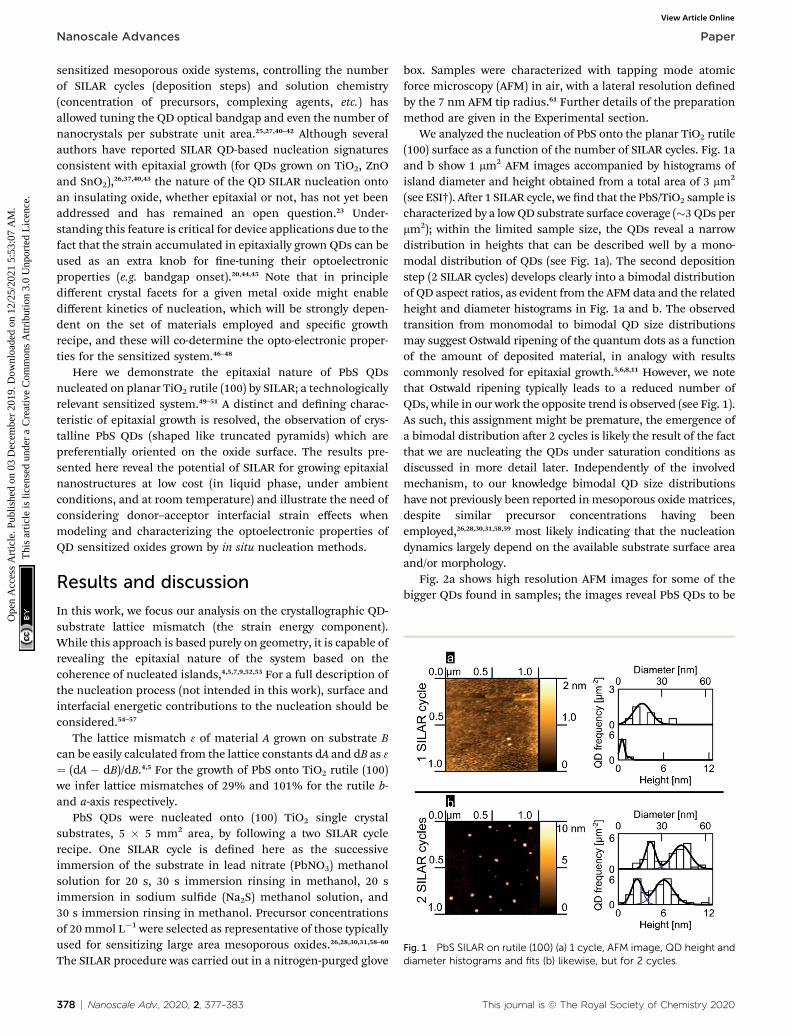
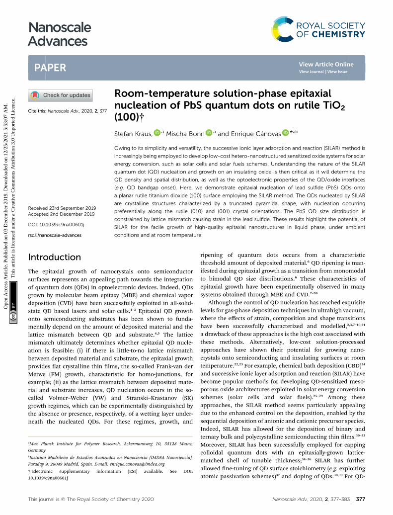
Fig. 1 PbS SILAR on rutile (100) (a) 1 cycle, AFM image, QD height anddiameter histograms and fits (b) likewise, but for 2 cycles.
Nanoscale Advances Paper
Ope
n A
cces
s A
rtic
le. P
ublis
hed
on 0
3 D
ecem
ber
2019
. Dow
nloa
ded
on 1
2/25
/202
1 5:
53:0
7 A
M.
Thi
s ar
ticle
is li
cens
ed u
nder
a C
reat
ive
Com
mon
s A
ttrib
utio
n 3.
0 U
npor
ted
Lic
ence
.View Article Online
sensitized mesoporous oxide systems, controlling the numberof SILAR cycles (deposition steps) and solution chemistry(concentration of precursors, complexing agents, etc.) hasallowed tuning the QD optical bandgap and even the number ofnanocrystals per substrate unit area.25,27,40–42 Although severalauthors have reported SILAR QD-based nucleation signaturesconsistent with epitaxial growth (for QDs grown on TiO2, ZnOand SnO2),26,37,40,43 the nature of the QD SILAR nucleation ontoan insulating oxide, whether epitaxial or not, has not yet beenaddressed and has remained an open question.23 Under-standing this feature is critical for device applications due to thefact that the strain accumulated in epitaxially grown QDs can beused as an extra knob for ne-tuning their optoelectronicproperties (e.g. bandgap onset).20,44,45 Note that in principledifferent crystal facets for a given metal oxide might enabledifferent kinetics of nucleation, which will be strongly depen-dent on the set of materials employed and specic growthrecipe, and these will co-determine the opto-electronic proper-ties for the sensitized system.46–48
Here we demonstrate the epitaxial nature of PbS QDsnucleated on planar TiO2 rutile (100) by SILAR; a technologicallyrelevant sensitized system.49–51 A distinct and dening charac-teristic of epitaxial growth is resolved, the observation of crys-talline PbS QDs (shaped like truncated pyramids) which arepreferentially oriented on the oxide surface. The results pre-sented here reveal the potential of SILAR for growing epitaxialnanostructures at low cost (in liquid phase, under ambientconditions, and at room temperature) and illustrate the need ofconsidering donor–acceptor interfacial strain effects whenmodeling and characterizing the optoelectronic properties ofQD sensitized oxides grown by in situ nucleation methods.
Results and discussion
In this work, we focus our analysis on the crystallographic QD-substrate lattice mismatch (the strain energy component).While this approach is based purely on geometry, it is capable ofrevealing the epitaxial nature of the system based on thecoherence of nucleated islands,4,5,7,9,52,53 For a full description ofthe nucleation process (not intended in this work), surface andinterfacial energetic contributions to the nucleation should beconsidered.54–57
The lattice mismatch 3 of material A grown on substrate Bcan be easily calculated from the lattice constants dA and dB as 3¼ (dA � dB)/dB.4,5 For the growth of PbS onto TiO2 rutile (100)we infer lattice mismatches of 29% and 101% for the rutile b-and a-axis respectively.
PbS QDs were nucleated onto (100) TiO2 single crystalsubstrates, 5 � 5 mm2 area, by following a two SILAR cyclerecipe. One SILAR cycle is dened here as the successiveimmersion of the substrate in lead nitrate (PbNO3) methanolsolution for 20 s, 30 s immersion rinsing in methanol, 20 simmersion in sodium sulde (Na2S) methanol solution, and30 s immersion rinsing in methanol. Precursor concentrationsof 20 mmol L�1 were selected as representative of those typicallyused for sensitizing large area mesoporous oxides.26,28,30,31,58–60
The SILAR procedure was carried out in a nitrogen-purged glove
378 | Nanoscale Adv., 2020, 2, 377–383
box. Samples were characterized with tapping mode atomicforce microscopy (AFM) in air, with a lateral resolution denedby the 7 nm AFM tip radius.61 Further details of the preparationmethod are given in the Experimental section.
We analyzed the nucleation of PbS onto the planar TiO2 rutile(100) surface as a function of the number of SILAR cycles. Fig. 1aand b show 1 mm2 AFM images accompanied by histograms ofisland diameter and height obtained from a total area of 3 mm2
(see ESI†). Aer 1 SILAR cycle, we nd that the PbS/TiO2 sample ischaracterized by a lowQD substrate surface coverage (�3 QDs permm2); within the limited sample size, the QDs reveal a narrowdistribution in heights that can be described well by a mono-modal distribution of QDs (see Fig. 1a). The second depositionstep (2 SILAR cycles) develops clearly into a bimodal distributionof QD aspect ratios, as evident from the AFM data and the relatedheight and diameter histograms in Fig. 1a and b. The observedtransition from monomodal to bimodal QD size distributionsmay suggest Ostwald ripening of the quantum dots as a functionof the amount of deposited material, in analogy with resultscommonly resolved for epitaxial growth.5,6,8,11 However, we notethat Ostwald ripening typically leads to a reduced number ofQDs, while in our work the opposite trend is observed (see Fig. 1).As such, this assignment might be premature, the emergence ofa bimodal distribution aer 2 cycles is likely the result of the factthat we are nucleating the QDs under saturation conditions asdiscussed in more detail later. Independently of the involvedmechanism, to our knowledge bimodal QD size distributionshave not previously been reported inmesoporous oxide matrices,despite similar precursor concentrations having beenemployed,26,28,30,31,58,59 most likely indicating that the nucleationdynamics largely depend on the available substrate surface areaand/or morphology.
Fig. 2a shows high resolution AFM images for some of thebigger QDs found in samples; the images reveal PbS QDs to be
This journal is © The Royal Society of Chemistry 2020
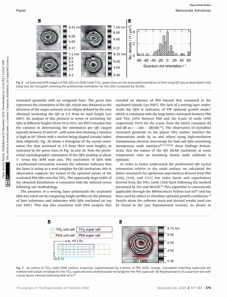
Fig. 2 (a) Selected AFM images of PbS QDs on (100) rutile TiO2; green lines are the estimated orientation of their long QD axis as described in thebody text (b) histogram showing the preferential orientation for the QDs nucleated by SILARs.
Paper Nanoscale Advances
Ope
n A
cces
s A
rtic
le. P
ublis
hed
on 0
3 D
ecem
ber
2019
. Dow
nloa
ded
on 1
2/25
/202
1 5:
53:0
7 A
M.
Thi
s ar
ticle
is li
cens
ed u
nder
a C
reat
ive
Com
mon
s A
ttrib
utio
n 3.
0 U
npor
ted
Lic
ence
.View Article Online
truncated pyramids with an octagonal base. The green linerepresents the orientation of the QD, which was obtained as thedirection of the major semiaxis of an ellipse dened by the areaobtained sectioning the QD at 1/4 from its total height (seeESI†). An analysis of this protocol in terms of sectioning theQDs at different heights (from 50 to 95%, see ESI†) revealed thatthe variance in determining the orientation per QD rangedtypically between 10 and 20�, with some dots showing a varianceis high as 60� (those with a section being shaped circular ratherthan elliptical). Fig. 2b shows a histogram of the crystal orien-tation (for dots sectioned at 1/4 from their total height), asindicated by the green lines in Fig. 2a and 3b. Note the prefer-ential crystallographic orientation of the QDs peaking at about5� versus the AFM scan axis. The nucleation of QDs witha preferential orientation towards the substrate indicates thatthe latter is acting as a seed template for QD nucleation; this isobservation supports the notion of the epitaxial nature of thenucleated PbS QDs onto at TiO2. The apparently large width ofthe obtained distribution is consistent with the inferred errorsfollowing our methodology.
The presence of a wetting layer underneath the nucleatedQDs was ruled out by comparing height proles on the plateausof bare substrates and substrates with QDs nucleated on top(see ESI†). This was also consistent with EDX analysis that
Fig. 3 (a) Lattice of TiO2 rutile (100) surface, turquoise, superimposedmarked with a blue rectangle for the TiO2 supercell and a dotted purple recrystal facets inferred following Moll et al.53
This journal is © The Royal Society of Chemistry 2020
revealed an absence of PbS beyond that contained in thenucleated islands (see ESI†). The lack of a wetting layer under-neath the QDs is indicative of VW epitaxial growth mode,5
which is consistent with the large lattice mismatch between PbSand TiO2 (29% between PbS and the b-axis of rutile (100)respectively 101% for the a-axis, from the lattice constants dAand dB as 3 ¼ (dA � dB)/dB.4,5). The observation of crystallinetruncated pyramids on the planar TiO2 surface matches theobservations made by us and others using high-resolutiontransmission electron microscopy for lead salt QDs sensitizingmesoporous oxide matrices;26,37,53,62,63 these ndings demon-strate that the nature of the QD SILAR nucleation at roomtemperature onto an insulating titania oxide substrate isepitaxial.
In order to better understand the preferential QD crystalorientation relative to the oxide surface, we calculated thelattice mismatch for optimized superlattices derived from PbS(100), (110), and (111) low index facets and superlatticesderived from the TiO2 rutile (100) facet following the methodpresented by Zur and McGill.64 This algorithm is convenientlyapplicable through the MPInterfaces Python tool set65 and hasbeen used by others to elucidate epitaxial growth conditions.22
Details about the soware stack and derived results used canbe found in the (see Experimental section). As shown in
by a lattice of PbS (100), orange. Calculated matching supercells arectangle for the PbS supercell. (b) Representation of a quantum dot with
Nanoscale Adv., 2020, 2, 377–383 | 379
Nanoscale Advances Paper
Ope
n A
cces
s A
rtic
le. P
ublis
hed
on 0
3 D
ecem
ber
2019
. Dow
nloa
ded
on 1
2/25
/202
1 5:
53:0
7 A
M.
Thi
s ar
ticle
is li
cens
ed u
nder
a C
reat
ive
Com
mon
s A
ttrib
utio
n 3.
0 U
npor
ted
Lic
ence
.View Article Online
Fig. 3a, for a TiO2 (100) supercell area of up to 400 A2 we nd analmost perfect lattice matching with the (100) lattice of PbS fora supercell area of 245 A2 containing 7 unit cells of PbS (100)and 18 unit cells of TiO2 rutile (100) (vector mismatches forthis optimized solution are 3u ¼ 0.3% and 3v ¼ 0.5%). Theseestimates of the mismatch and orientation strongly supportthe suitability of epitaxial growth of PbS (100) onto TiO2 rutile(100). Note that epitaxial nucleation was resolved for PbSe QDs(002) on Fe2O3 (003),22 a system characterized by larger latticemismatches along preferential oxide axis (0.7% and 3.2% ina and b directions; 220 A2 cell area). In our systems a smallermismatch along the c-axis can be linked with the strain alongthe c-axis being smaller, thus leading to a preferred growthalong that crystal axis. In Fig. 3b we show in red the most likelyQD crystal orientation taking into account the availableexperimental data and modelling.
Finally, it is worth noting that under our experimentalconditions, we also identied PbS rod-like structures togetherwith the QDs shown in Fig. 1 and 2; we speculate this is due tothe high precursor concentrations (PCs) employed in our rela-tively small-area samples.50 To date, region-selective growth ofnanostructures by SILAR remains a challenge,.66 However, fewreports have indeed resolved the nucleation of rod-wire likestructures by SILAR, in an isolated fashion67 or together withQDs onto a mesoporous titania electrode.68 Notably, in all thesereports, anisotropic growth has been linked with nucleationunder saturation conditions (in agreement with our ndings);specically, some control over the nucleation of rod-wirestructures was achieved by depositing the samples under non-stoichiometric conditions (with cation/anion ratios larger than1). We speculate that the titania substrate might be catalyzingthis effect, i.e. SILAR rinsing steps might be unable tocompletely remove the excess of precursors and this imbalancemight promote the formation of rod-like structures. Certainly,further studies are needed to ascertain, among other aspects,the generation of a saturated bi-modal distribution of QD sizesaer only two SILAR cycles. In any case, while the nucleation ofour QDs is happening under saturation conditions, we believethat the main result of our work is not compromised, i.e. thedemonstration that epitaxy of QDs onto a rutile titania surfaceby SILAR is feasible at room temperature. Our ndings agreewith work from Lau et al.69 who reported epitaxial growth of PbSnanowires using CVD on TiO2 rutile (001) obeying VW growth.These ndings seem to illustrate that the formation of epitaxialrods is accessible by SILAR and can offer a platform for in situpreparation of rod-sensitized mesoporous oxides to comple-ment ex situ rod sensitization schemes previously reported byothers.70 Clearly, further work is needed to interrogate in detailthe impact of immersion times, precursor concentration,substrate area to PC ratio and PC temperature on the nucleationof QDs grown by SILAR, thus paving the road for SILAR as fast,simple and reliable synthesis method for epitaxial QD growth asan addition to the established ultra-high vacuum methods.Future work should also consider other crystal facet combina-tions as QDs are commonly grown on mesoporous substratesthat naturally exhibit more than the (100) surface of TiO2
rutile.49
380 | Nanoscale Adv., 2020, 2, 377–383
ExperimentalSILAR procedure
Chromatography grade methanol (CH3OH) was obtained fromVWR. Analytical reagent grade acetone was obtained fromFisher Chemical. Lead nitrate (Pb(NO3)2) 99%, anhydroussodium sulde (Na2S) 98% and puriss. p.a. 2-propanol wereobtained from Sigma-Aldrich. Dissolved gaseous oxygen wasremoved from methanol by bubbling argon through it for onehour and precursor solutions were prepared. 20 mmol L�1 leadnitrate and sodium sulde solutions were used as precursorsolutions. Rutile (TiO2) single crystals 10 mm by 5 mm by 0.5mm, (100) faced were obtained from Crystal GmbH, Berlin,Germany. Sample substrates were sonicated in acetone for 15minutes and for another 15 minutes in 2-propanol. SILAR wascarried out in a nitrogen glovebox. Prior to starting with theSILAR cycles every substrate was immersed 30 s in fresh meth-anol. 1 SILAR cycle consisted of 20 s immersion in lead nitratesolution, 30 s immersion in methanol, 20 s immersion insodium sulde solution and 30 s immersion in methanol. Aercompleting the desired number of SILAR cycles the substrateswere immersed for 50 s in fresh methanol and dried in theglovebox. AFM images were recorded with a Bruker MultiModeequipped with a NanoScope 3a controller or a NanoScope 5controller.
Atomic force microscopy
The AFMs were operated in tapping mode with cantilevers oftype OMCL-AC160TS (resonance frequency ¼ (300 � 100) kHz,typical tip radius ¼ 7 nm) from Olympus, limiting the lateralresolution. Our data analysis is based on binning lateral datainto 5 nm wide bins and height data into 1 nm wide bins. Thusthe assumed accuracies are 5 nm for lateral measurements and1 nm for vertical measurements. AFM images were analyzedusing the soware package Gwyddion. QDs were marked usinga height threshold mask in Gwyddion, the diameter and heightof the QDs were exported to generate histograms. Fitting twoGaussians to the histograms gave the diameter and heightdistributions included in the subpanels of Fig. 1. For details onthe tting procedure and AFM data processing see ESI.†
Computation of lattice matched super cells
The reduction algorithm published by Zur and McGill wasimplemented using Python 3.5.2 and NumPy 1.11.1. This self-written implementation was used to check the correct reduc-tion of the results from the supercell search performed with theMPInterfaces 1.2.0 package65 running Python 3.5.2.71 Furtherdependencies were imported in the following versions: pymat-gen 3.7.1,72 Atomic Simulation Environment (ASE) 3.11.0,67
NumPy 1.11.1.73 To get the unit cells Structure.from_le() fromthe pymatgen.core.structure module was used to import cif-lesobtained from the American Mineralogist Crystal StructureDatabase74 (PbS:75 Database Code 0011372, TiO2 rutile:76 Data-base Code 0009404). The Interface method from the mpinter-faces.interface module was used to calculate the lattice vectorsof the two material facets investigated that are dened by the
This journal is © The Royal Society of Chemistry 2020
Paper Nanoscale Advances
Ope
n A
cces
s A
rtic
le. P
ublis
hed
on 0
3 D
ecem
ber
2019
. Dow
nloa
ded
on 1
2/25
/202
1 5:
53:0
7 A
M.
Thi
s ar
ticle
is li
cens
ed u
nder
a C
reat
ive
Com
mon
s A
ttrib
utio
n 3.
0 U
npor
ted
Lic
ence
.View Article Online
given unit cells and miller indices. Finally the best matchingsupercells were searched with the get_matching_latticesmethod from the mpinterfaces.transformations module usingfollowing constraints: max_area ¼ 400, max_mismatch ¼ 0.01,max_angle_diff ¼ 1, r1r2_tol ¼ 0.2. The hkl triple for TiO2 rutileas substrate was always set to (1, 0, 0). Three different hkl triplesfor PbS were investigated and the following lattice matchingsupercells were identied to fulll the constraints. For PbS(100): supercell area A ¼ 245 A2, 18 substrate unit cells, 7 PbS(100) unit cells, lattice vector mismatch u 3u ¼ 0.00311, latticevector mismatch v 3v ¼ 0.00499, angle between u and v: both90�. For PbS (110): A¼ 299 A2, 22 substrate unit cells, 6 PbS (110)unit cells, 3u ¼ 0.00311, 3v ¼ �0.00326, angle between u and v:both 90�. For PbS (111) no match was found within the usedconstraints.
Conclusions
In conclusion, we have demonstrated that the nature of PbSQDs nucleated on TiO2 (100) by SILAR obeys epitaxy. Thephysics underlying the nucleation of nanocrystals at roomtemperature achieved by SILAR share the key characteristics ofthose reported for ultra-high vacuum and high-temperaturemethods like MBE and CVD. Our results have importantimplications for the design of nanostructured solar energyconversion schemes (e.g. solar cells and fuels); the strain accu-mulation during QD nucleation needs to be considered asa factor affecting structural (e.g. QD size and shape) and opto-electronic properties (e.g. bandgap) in QD sensitized oxidegeometries. Owing to its rather simple preparative conditionsand versatility, SILAR has great further promise for the growthof high-quality epitaxial nanostructures in liquid phase, underambient conditions and at room temperature.
Conflicts of interest
There are no conicts to declare.
Acknowledgements
E. C. acknowledges nancial support from the Max PlanckGraduate Center and the regional government of Comunidad deMadrid under project (2017-T1/AMB-5207). We thank RudigerBerger, Uwe Rietzler and Helma Burg (MPI-P) for their experthelp and fruitful discussions around atomic force microscopyand Gunnar Glaßer for SEM and EDX. E. C. acknowledgesnancial support from the Max Planck Society, the regionalgovernment of Comunidad de Madrid (2017-T1/AMB-5207) andthe “Severo Ochoa” Programme for Centres of Excellence inR&D (MINECO, Grant No. SEV-2016-0686).
Notes and references
1 A. Martı, E. Antolın, C. R. Stanley, C. D. Farmer, N. Lopez,P. Dıaz, E. Canovas, P. G. Linares and A. Luque, Phys. Rev.Lett., 2006, 97(24), 247701, DOI: 10.1103/PhysRevLett.97.247701.
This journal is © The Royal Society of Chemistry 2020
2 A. Banerjee, T. Frost, S. Jahangir, E. Stark andP. Bhattacharya, J. Cryst. Growth, 2013, 378, 566, DOI:10.1016/j.jcrysgro.2012.12.158.
3 F. Heinrichsdorff, M.-H. Mao, N. Kirstaedter, A. Krost,D. Bimberg, A. O. Kosogov and P. Werner, Appl. Phys. Lett.,1997, 71(1), 22, DOI: 10.1063/1.120556.
4 I. Daruka and A.-L. Barabasi, Phys. Rev. Lett., 1997, 79(19),3708, DOI: 10.1103/PhysRevLett.79.3708.
5 I. Daruka and A.-L. Barabasi, Appl. Phys. Lett., 1998, 72(17),2102, DOI: 10.1063/1.121289.
6 M. Petersen, A. Zangwill and C. Ratsch, Surf. Sci., 2003,536(1–3), 55, DOI: 10.1016/S0039-6028(03)00580-6.
7 D. Leonard, K. Pond and P. M. Petroff, Phys. Rev. B: Condens.Matter Mater. Phys., 1994, 50(16), 11687, DOI: 10.1103/PhysRevB.50.11687.
8 T. R. Ramachandran, R. Heitz, P. Chen and A. Madhukar,Appl. Phys. Lett., 1997, 70(5), 640, DOI: 10.1063/1.118848.
9 A. Balzarotti, Nanotechnology, 2008, 19(50), 505701, DOI:10.1088/0957-4484/19/50/505701.
10 S. L. Murray, F. D. Newman, C. S. Murray, D. M. Wilt,M. W. Wanlass, P. Ahrenkiel, R. Messham andR. R. Siergiej, Semicond. Sci. Technol., 2003, 18(5), S202,DOI: 10.1088/0268-1242/18/5/309.
11 B. Bansal, M. R. Gokhale, A. Bhattacharya and B. M. Arora, J.Appl. Phys., 2007, 101(9), 094303.
12 C. J. Elliott, E. A. Chekhovich, A. B. Krysa, M. S. Skolnick andA. I. Tartakovskii, J. Phys.: Conf. Ser., 2010, 245(1), 012061,DOI: 10.1088/1742-6596/245/1/012061.
13 D. Barbadikar, R. Gautam, S. Sahare, R. Patrikar and J. Bhatt,Bull. Mater. Sci., 2013, 36(3), 483, DOI: 10.1007/s12034-013-0487-7.
14 M. Kasu and N. Kobayashi, Jpn. J. Appl. Phys., 1994, 33(1S),712, DOI: 10.1143/JJAP.33.712.
15 I. Kegel, T. H. Metzger, A. Lorke, J. Peisl, J. Stangl, G. Bauer,J. M. Garcıa and P. M. Petroff, Phys. Rev. Lett., 2000, 85(8),1694, DOI: 10.1103/PhysRevLett.85.1694.
16 K. L. Choy, Prog. Mater. Sci., 2003, 48(2), 57, DOI: 10.1016/S0079-6425(01)00009-3.
17 L. Esaki in Molecular Beam Epitaxy and Heterostructures, ed.L. L. Chang and K. Ploog, Springer, Dodrecht, Netherlands,1985, p. 1, DOI: 10.1007/978-94-009-5073-3_1.
18 D. Bimberg, M. Grundmann and N. N. Ledencov, QuantumDot Heterostructures, Wiley, Chichester, UK, 1999.
19 J. R. Arthur, Surf. Sci., 2002, 500(1–3), 189, DOI: 10.1016/S0039-6028(01)01525-4.
20 M. Grundmann, O. Stier and D. Bimberg, Phys. Rev. B:Condens. Matter Mater. Phys., 1995, 52(16), 11969, DOI:10.1103/PhysRevB.52.11969.
21 N. u. H. Alvi, P. E. D. Soto Rodriguez, P. Aseev, V. J. Gomez,A. u. H. Alvi, W. u. Hassan, M. Willander and R. Notzel, NanoEnergy, 2015, 13, 291, DOI: 10.1016/j.nanoen.2015.02.017.
22 R. S. Selinsky, S. Shin, M. A. Lukowski and S. Jin, J. Phys.Chem. Lett., 2012, 3(12), 1649, DOI: 10.1021/jz300672x.
23 R. S. Selinsky, Q. Ding, M. S. Faber, J. C. Wright and S. Jin,Chem. Soc. Rev., 2013, 42(7), 2963, DOI: 10.1039/C2CS35374A.
24 C.-H. Chang and Y.-L. Lee, Appl. Phys. Lett., 2007, 91(5),053503, DOI: 10.1063/1.2768311.
Nanoscale Adv., 2020, 2, 377–383 | 381
Nanoscale Advances Paper
Ope
n A
cces
s A
rtic
le. P
ublis
hed
on 0
3 D
ecem
ber
2019
. Dow
nloa
ded
on 1
2/25
/202
1 5:
53:0
7 A
M.
Thi
s ar
ticle
is li
cens
ed u
nder
a C
reat
ive
Com
mon
s A
ttrib
utio
n 3.
0 U
npor
ted
Lic
ence
.View Article Online
25 H. Lee, M. Wang, P. Chen, D. R. Gamelin, S. M. Zakeeruddin,M. Gratzel and M. K. Nazeeruddin, Nano Lett., 2009, 9(12),4221, DOI: 10.1021/nl902438d.
26 H. Lee, H. C. Leventis, S.-J. Moon, P. Chen, S. Ito,S. A. Haque, T. Torres, F. Nuesch, T. Geiger,S. M. Zakeeruddin, M. Gratzel and M. K. Nazeeruddin, Adv.Funct. Mater., 2009, 19(17), 2735, DOI: 10.1002/adfm.200900081.
27 H. J. Snaith, A. Stavrinadis, P. Docampo and A. A. Watt, Sol.Energy, 2011, 85(6), 1283, DOI: 10.1016/j.solener.2011.01.019.
28 Q. Kang, S. Liu, L. Yang, Q. Cai and C. A. Grimes, ACS Appl.Mater. Interfaces, 2011, 3(3), 746, DOI: 10.1021/am101086t.
29 R. Vogel, P. Hoyer and H. Weller, J. Phys. Chem., 1994, 98(12),3183, DOI: 10.1021/j100063a022.
30 Y. F. Nicolau, Appl. Surf. Sci., 1985, 22–23, 1061, DOI:10.1016/0378-5963(85)90241-7.
31 T. Kanniainen, S. Lindroos, J. Ihanus and M. Leskela, J.Mater. Chem., 1996, 6(2), 161, DOI: 10.1039/JM9960600161.
32 T. Kanniainen, S. Lindroos, J. Ihanus and M. Leskela, J.Mater. Chem., 1996, 6(6), 983, DOI: 10.1039/jm9960600983.
33 H. M. Pathan and C. D. Lokhande, Bull. Mater. Sci., 2004,27(2), 85, DOI: 10.1007/BF02708491.
34 Y. Zhang, J. Zhu, X. Yu, J. Wei, L. Hu and S. Dai, Sol. Energy,2012, 86(3), 964, DOI: 10.1016/j.solener.2012.01.006.
35 J. J. Li, Y. A. Wang, W. Guo, J. C. Keay, T. D. Mishima,M. B. Johnson and X. Peng, J. Am. Chem. Soc., 2003,125(41), 12567, DOI: 10.1021/ja0363563.
36 R. G. Xie, U. Kolb, J. X. Li, T. Basche and A. Mews, J. Am.Chem. Soc., 2005, 127(20), 7480, DOI: 10.1021/ja042939g.
37 H. Wang, I. Barcelo, T. Lana-Villarreal, R. Gomez, M. Bonnand E. Canovas, Nano Lett., 2014, 14(10), 5780, DOI:10.1021/nl5026634.
38 Y. Gulen, Metall. Mater. Trans. A, 2015, 46(10), 4698, DOI:10.1007/s11661-015-3065-3.
39 A. E. Jimenez-Gonzalez, J. Solid State Chem., 1997, 128(2),176, DOI: 10.1006/jssc.1996.7166.
40 I. Barcelo, T. Lana-Villarreal and R. Gomez, J. Photochem.Photobiol., A, 2011, 220(1), 47, DOI: 10.1016/j.jphotochem.2011.03.016.
41 I. Barcelo, J. M. Campina, T. Lana-Villarreal and R. Gomez,Phys. Chem. Chem. Phys., 2012, 14(16), 5801, DOI: 10.1039/C2CP40609H.
42 S. Wang, W. Dong, X. Fang, S. Wu, R. Tao, Z. Deng, J. Shao,L. Hu and J. Zhu, J. Power Sources, 2015, 273(0), 645, DOI:10.1016/j.jpowsour.2014.09.148.
43 N. Guijarro, T. Lana-Villarreal, T. Lutz, S. A. Haque andR. Gomez, J. Phys. Chem. Lett., 2012, 3(22), 3367, DOI:10.1021/jz301528a.
44 H. Jiang and J. Singh, Phys. Rev. B: Condens. Matter Mater.Phys., 1997, 56(8), 4696, DOI: 10.1103/PhysRevB.56.4696.
45 A. M. Smith, A. M. Mohs and S. Nie, Nat. Nanotechnol., 2009,4(1), 56, DOI: 10.1038/nnano.2008.360.
46 A. M. Smith, A. M. Mohs and S. Nie, Nat. Nanotechnol., 2009,4(1), 56, DOI: 10.1038/nnano.2008.360.
47 A. M. Smith, A. M. Mohs and S. Nie, Nat. Nanotechnol., 2009,4(1), 56, DOI: 10.1038/nnano.2008.360.
382 | Nanoscale Adv., 2020, 2, 377–383
48 A. M. Smith, A. M. Mohs and S. Nie, Nat. Nanotechnol., 2009,4(1), 56, DOI: 10.1038/nnano.2008.360.
49 B. Ohtani, O. O. Prieto-Mahaney, D. Li and R. Abe, J.Photochem. Photobiol., A, 2010, 216(2–3), 179, DOI: 10.1016/j.jphotochem.2010.07.024.
50 J. Zhang, M. Brehm, M. Grydlik and O. G. Schmidt, Chem.Soc. Rev., 2015, 44(1), 26, DOI: 10.1039/c4cs00077c.
51 M. Pinczolits, G. Springholz and G. Bauer, Appl. Phys. Lett.,1998, 73(2), 250, DOI: 10.1063/1.121770.
52 U. W. Pohl, Epitaxy of Semiconductors: Introduction to PhysicalPrinciples, Springer Science & Business Media, 2013, DOI:10.1007/978-3-642-32970-8.
53 N. Moll, M. Scheffler and E. Pehlke, Phys. Rev. B: Condens.Matter Mater. Phys., 1998, 58(8), 4566, DOI: 10.1103/PhysRevB.58.4566.
54 M. Ohring, Materials Science of Thin Films, Elsevier Science,2001, DOI: 10.1016/B978-0-12-524975-1.50018-5.
55 D. Smith, Thin-Film Deposition: Principles and Practice,McGraw-Hill Education, 1995.
56 J. A. Venables, Introduction to Surface and Thin Film Processes,Cambridge University Press, 2000, DOI: 10.1017/CBO9780511755651.
57 B. W. Wessels, J. Vac. Sci. Technol., B: Nanotechnol.Microelectron.: Mater., Process., Meas., Phenom., 1997, 15(4),1056, DOI: 10.1116/1.589392.
58 T. Kanniainen, S. Lindroos, R. Resch, M. Leskela,G. Friedbacher and M. Grasserbauer, Mater. Res. Bull.,2000, 35(7), 1045, DOI: 10.1016/S0025-5408(00)00298-1.
59 T. Kanniainen, Studies of Zinc and Lead Chalcogenide ThinFilms Grown by SILAR (Successive Ionic Layer Adsorptionand Reaction) Technique, Ph.D. thesis, University ofHelsinki, Finland, 2001.
60 T. L. Remadevi and K. C. Preetha, J. Mater. Sci.: Mater.Electron., 2012, 23(11), 2017, DOI: 10.1007/s10854-012-0696-7.
61 P. Klapetek, M. Valtr, D. Necas, O. Salyk and P. Dzik,Nanoscale Res. Lett., 2011, 6(1), 514, DOI: 10.1186/1556-276X-6-514.
62 H. Choi, J.-H. Ko, Y.-H. Kim and S. Jeong, J. Am. Chem. Soc.,2013, 135(14), 5278, DOI: 10.1021/ja400948t.
63 A. Querejeta-Fernandez, J. C. Hernandez-Garrido, H. Yang,Y. Zhou, A. Varela, M. Parras, J. J. Calvino-Gamez,J. M. Gonzalez-Calbet, P. F. Green and N. A. Kotov, ACSNano, 2012, 6(5), 3800, DOI: 10.1021/nn300890s.
64 A. Zur and T. C. McGill, J. Appl. Phys., 1984, 55(2), 378, DOI:10.1063/1.333084.
65 K. Mathew, A. K. Singh, J. J. Gabriel, K. Choudhary,S. B. Sinnott, A. V. Davydov, F. Tavazza and R. G. Hennig,Comput. Mater. Sci., 2016, 122, 183, DOI: 10.1016/j.commatsci.2016.05.020.
66 Anisotropic and Shape-Selective Nanomaterials,Nanostructure Science and Technology, Chapter 7 -Prospects for Rational Control of Nanocrystal Shape ThroughSuccessive Ionic Layer Adsorption and Reaction (SILAR) andRelated Approaches, ed. S. E. Hunyadi Murphy, 2017, DOI:10.1007/978-3-319-59662-4_7.
This journal is © The Royal Society of Chemistry 2020
Paper Nanoscale Advances
Ope
n A
cces
s A
rtic
le. P
ublis
hed
on 0
3 D
ecem
ber
2019
. Dow
nloa
ded
on 1
2/25
/202
1 5:
53:0
7 A
M.
Thi
s ar
ticle
is li
cens
ed u
nder
a C
reat
ive
Com
mon
s A
ttrib
utio
n 3.
0 U
npor
ted
Lic
ence
.View Article Online
67 R. S. Dariani and F. Salehi, Mater. Res. Express, 2016, 3,05501.
68 S. Piri Pishekloo, R. S. Dariani and F. Salehi, Mater. Sci.Semicond. Process., 2016, 43, 182, DOI: 10.1016/j.mssp.2015.12.021.
69 Y. K. A. Lau, D. J. Chernak, M. J. Bierman and S. Jin, J. Mater.Chem., 2009, 19(7), 934, DOI: 10.1039/B818187J.
70 A. Salant, M. Shalom, Z. Tachan, S. Buhbut, A. Zaban andU. Bani, Nano Lett., 2012, 12(4), 2095, DOI: 10.1021/nl300356e.
71 K. J. Millman and M. Aivazis, Comput. Sci. Eng., 2011, 13(2),9, DOI: 10.1109/mcse.2011.36.
This journal is © The Royal Society of Chemistry 2020
72 S. P. Ong, W. D. Richards, A. Jain, G. Hautier, M. Kocher,S. Cholia, D. Gunter, V. L. Chevrier, K. A. Persson andG. Ceder, Comput. Mater. Sci., 2013, 68, 314, DOI: 10.1016/j.commatsci.2012.10.028.
73 S. R. Bahn and K. W. Jacobsen, Comput. Sci. Eng., 2002, 4(3),56, DOI: 10.1109/5992.998641.
74 R. T. Downs and M. Hall-Wallace, Am. Mineral., 2003, 88(1),247.
75 R. W. G. Wyckoff, Crystal Structures, Interscience Publ, NewYork, 1963.
76 W. H. Baur and A. A. Khan, Acta Crystallogr., Sect. B: Struct.Crystallogr. Cryst. Chem., 1971, 27(11), 2133, DOI: 10.1107/S0567740871005466.
Nanoscale Adv., 2020, 2, 377–383 | 383


![Temperature‐dependent Nucleation and Growth of Dendrite‐Free … · nucleation, chronoamperometry has been used to model heterogeneous nucleation behavior.[10] Therefore, we further](https://img.pdfslide.us/doc/110x75/5ecedb8e0e2bd5210370ca09/temperatureadependent-nucleation-and-growth-of-dendriteafree-nucleation-chronoamperometry.jpg)