Embed Size (px)
Citation preview

Roll Printed Electronics: Development and Scaling of
Gravure Printing Techniques
Alejandro De la Fuente Vornbrock
Electrical Engineering and Computer SciencesUniversity of California at Berkeley
Technical Report No. UCB/EECS-2009-191
http://www.eecs.berkeley.edu/Pubs/TechRpts/2009/EECS-2009-191.html
December 29, 2009

Copyright © 2009, by the author(s).All rights reserved.
Permission to make digital or hard copies of all or part of this work forpersonal or classroom use is granted without fee provided that copies arenot made or distributed for profit or commercial advantage and that copiesbear this notice and the full citation on the first page. To copy otherwise, torepublish, to post on servers or to redistribute to lists, requires prior specificpermission.
Roll Printed Electronics: Development and Scaling of Gravure Printing Techniques
by
Alejandro de la Fuente Vornbrock
A dissertation submitted in partial satisfaction of the
Requirements for the degree of
Doctor of Philosophy
in
Engineering - Electrical Engineering and Computer Sciences
in the
Graduate Division
of the
University of California, Berkeley
Committee in charge:
Professor Vivek Subramanian, Chair
Professor Tsu-Jae King Liu
Professor David Dornfeld
Fall 2009

Roll Printed Electronics: Development and Scaling of Gravure Printing Techniques
© Copyright 2009 by
Alejandro de la Fuente Vornbrock
1
Abstract
Roll Printed Electronics: Development and Scaling of Gravure Printing Techniques by
Alejandro de la Fuente Vornbrock Doctor of Philosophy in Engineering ‐ Electrical Engineering and Computer Sciences
University of California, Berkeley Professor Vivek Subramanian, Chair
To realize the potential cost savings promised by printed electronics, high‐speed, large‐volume manufacturing methods must be established. Rotary printing techniques such as those used in the graphic arts are ideal candidates. However, very little research has been done on utilizing these techniques for printed electronics because digital processes such ink‐jet printing have offered researchers a low‐cost flexible solution for demonstrating the printability of their materials, despite the fact that these processes may be difficult to scale for large‐volume manufacturing. In this thesis, gravure, a printing process which offers the highest resolution, highest speed, and largest volume production in the graphic arts is demonstrated as a viable technique for printed electronics. In order to make laboratory‐scale research with this technique possible, a custom table‐top gravure printing press was designed. This press allows for small amounts of ink to be utilized during a print and enables multi‐layer prints with a registration accuracy not seen in conventional gravure printing presses and suitable for printed electronics. With this press, printing processes to deposit functional materials for printed circuits are investigated with a focus on developing process modules to manufacture fully printed organic thin film transistors. Considerable effort is made to establish processes to deposit metallic lines with feature sizes below 20 μm and a total surface roughness below 20 nm, uniform thin films of polymer dielectrics with thicknesses as low as 70 nm, and high performance polymer semiconductors. These processes are then integrated to manufacture capacitors suitable for integrated circuit components and organic thin film transistors with operating frequencies as high as 18 kHz.
i
Acknowledgements I have been told many times, always by older, much wiser people than me, that the best job is a job you enjoy, and that it is generally the people who make it enjoyable. Despite how challenging graduate school was at times, I can say I truly enjoyed it and I have a great group of friends and colleagues to thank for that. There gravure project in general was an immense effort which involved a great number of people. Steve Molesa was my big brother in lab during my first years here at UC Berkeley and in great part this project got off the ground thanks to him. Here is to Steve for all of those days on the ink-jet printers. Early in the project I had the fortune of working with two great undergraduates, Li Li and Vincent Liu, who at one point where dubbed the “mad CADders” for the endless hours we spent designing the gravure printer. Li then went on to help me out with gravure roll patterning, and was a big help in getting over some hurdles with exposure and development. Another undergraduate, Jose Covarrubias, followed up by helping scale gravure feature sizes. Finally, I had the privilege to work with Donovan Sung. Donovan made great strides in advancing our patterning capability by making contacts with the gravure industry and getting some great collaborations set up all on his own. I owe him thanks and respect for the tenacity he has shown in pushing the project forward, getting things done, and meeting deadlines, especially when that meant he was sleeping on the couch. Of course, there would be no gravure printer without a machine shop, and I owe special thanks to Warner Carlisle, Bob Amaral, Joe Gavazza, and Ben Lake. Joe was the head machinist on my project and was my main point of contact when technical issues came up. He was always helpful, patient and friendly. To Ben Lake, I owe the greatest thanks. From the very beginning he bent over backwards to give us a very competitive bid, to make sure our project was well taken care of, and to make adjustments when I came back (so many times) with design changes and outrageous requests. Not only has Ben an example of willingness to help, he’s become a close friend. Also, I want to thank everyone for letting me sit with them and bother them with all sorts of obliquely work-related questions during their lunch breaks, it was great fun and I learned a lot from them. There was also a great deal of external help on this project that I must recognize and thank. Soligie in Savage, MN funded much of the printer development and early print research. WRE/ColorTech here in Berkeley and in Greensboro, NC was very helpful in providing us with patterned rolls and contacts through the industry. Mark Richter from Rotadyne Decorative Technologies made this project come together, as his attention to detail and standards of quality gave us the best gravure rolls we have used. Dr. Guido Hennig started our collaboration with Daetwyler and put us in touch with Eric Serenius, John Fraser, Lynn Petterson, and Kent Seibel who have worked hard to bring us the next generation of high-resolution gravure rolls. Finally, Erika Hrehorova from Western Michigan and Jay Sperry from Clemson have generously shared their knowledge and expertise in conventional printing with me. For their involvement with my thesis work I would like to thank Professors David Dornfeld, Tsu-Jae King Liu, Costas Grigoropoulos, and Costas Spanos. Professor Dornfeld has been of great help throughout the years especially in helping improve the quality of our gravure rolls, generously letting me use his equipment, and giving me hours of very fruitful discussion. I owe everything I know about precision design to him. Professor King has been a beacon of excellence for me, a great host during my first year, and has been incredibly generous in heading my qual committee and reading my thesis on such short notice. My lab mates have been a great part of the experience, and in them I have found great role models and friends. Everyone there my first year was so inspirational, and I owe thanks to Steve Volkman, Paul Chang, Josei Chang, Frank Liao, Brian Mattis, Steve Molesa, David Redinger, Daniel

ii
Huang, and Tuyen Le. I am quite sure I’ll never forget Steve Volkman’s creativity, Paul’s intelligence, and Josei and Frank’s efficiency. I also want to thank Shong Yin for being so generous and helpful these last few years, Huai-Yuan Tseng for the good times we spent printing together, and Dan Soltman for fruitful discussions on fluids. Through the years, though, I owe the most to Teymur Bakhishev, he has been a great lab mate and my best friend. I would also like to give thanks to my class-mates and friends; to John Secord, who was my roommate and close friend, and to Drew Carlson, Daniel Huang, Pankaj Kalra, Matthew Schoenecker, and Joe Makin, all of whom I learned a lot about how to be a better student and person from; to Donovan Lee for being such a good friend, for helping me so much in the last few months, and for motivating me to finish strong; to Raúl Aguilar, Eva Chapa, Armando Solar, Raúl Howe, and Homero Lara, for the laughs, the love, and support. I would have never gotten to Berkeley if it was not for a great undergraduate experience. I have to give special thanks to Prof. Richard Kiehl who took me under his wing since I was a sophomore at the University of Minnesota and taught me, much of it by personal tutelage, so much about science and research. My lab mates then were also very important and I owe thanks to Nikolai Nezlobin and Guanghua Xiao for being there to guide and help. I was also greatly inspired by my closest friends, Anthony Anderson and John McKeen, with whom I spent many hours talking about research and the wonders of science. Finally, I want to thank Prof. Anand Gopinath who had faith in me, and made me apply to the nation’s top schools and the NSF Fellowship. To my advisor, Prof. Vivek Subramanian, I owe my most sincere gratitude. He has always wished the very best for me, early on by encouraging me to think big and tackle problems that really matter, later, by teaching me that the purpose of the PhD is for me to exercise my leadership and take control over my own success, and throughout, by challenging me to strive for the highest level of quality. His vision has inspired me to always look for new uses for technology, and I give credit to him for the idea of using gravure. I am very grateful for the respect and the confidence he has placed in me, especially when that meant I would be standing in his place, or making him go and raise more funding. I only wish I could have done so much more for him. Finally, I want to thank my family. I have been so blessed to have such loving and caring parents and sisters. They have taught me so much about ethics, caring for the greater good, putting others before me, and most importantly, love. Mom, Dad, Sabrina, and Priscilla, this is for you.

iii
Contents 1 Introduction .............................................................................................................................. 1
1.1 The potential of printed electronics .............................................................................. 1
1.2 Conventional Printing Methods .................................................................................... 2
1.3 Goals ............................................................................................................................. 4
1.4 Background ................................................................................................................... 4
1.5 Organization ................................................................................................................. 5
1.6 Works Cited .................................................................................................................. 5
2 Gravure .................................................................................................................................... 7
2.1 Introduction .................................................................................................................. 7
2.1.1 Gravure printing fundamentals............................................................................................. 7 2.1.2 Table-Top Proof Presses and Laboratory Presses ................................................................. 9
2.2 A Laboratory Scale Gravure Printer for Printed Electronics ...................................... 10
2.2.1 Alignment Process and Sources of Error ............................................................................. 12 2.2.2 Experimental Position Repeatability and Alignment Accuracy ........................................... 14 2.2.3 Coupled Thermal Structural Analysis .................................................................................. 17 2.2.4 HTM Analysis ....................................................................................................................... 20 2.2.5 Discussion ............................................................................................................................ 28 2.2.6 Improvements ..................................................................................................................... 28 2.2.7 Error Analysis Summary ...................................................................................................... 31
2.3 Roll Patterning ............................................................................................................ 31
2.3.1 Materials and manufacturing of a gravure roll ................................................................... 32 2.3.2 Improved photolithographic patterning ............................................................................. 34 2.3.3 Surface polishing and effects on wiping and pattern fidelity ............................................. 36
2.4 Summary ..................................................................................................................... 37
2.5 Works Cited ................................................................................................................ 38
3 Printed Metal Lines ................................................................................................................ 39
3.1 Performance criteria for metallic lines ....................................................................... 39
3.1.1 Printed Circuit Boards ......................................................................................................... 39 3.1.2 Flexible Circuit Boards ......................................................................................................... 40 3.1.3 Back-end interconnects ...................................................................................................... 40 3.1.4 Contacts to devices ............................................................................................................. 41
3.2 Types of metallic inks................................................................................................. 41
3.3 Roughness of printed metal films and lines................................................................ 44
3.3.1 Roughness ........................................................................................................................... 45 3.3.2 Roughness of spun films ..................................................................................................... 48 3.3.3 Roughness of printed lines .................................................................................................. 52
3.4 Nanoparticle Silver lines for interconnects and device contacts ................................ 54
3.4.1 Experimental ....................................................................................................................... 55 3.4.2 Discussion/Print Considerations ......................................................................................... 57
iv
3.4.3 Results ................................................................................................................................. 58 3.4.4 Scaling ................................................................................................................................. 65 3.4.5 Remarks............................................................................................................................... 67
3.5 Organometallic Silver lines for device contacts ......................................................... 67
3.6 Summary ..................................................................................................................... 72
3.7 Works Cited ................................................................................................................ 73
4 Capacitors .............................................................................................................................. 75
4.1 Capacitor structure and role in ICs ............................................................................. 75
4.2 Dielectrics in Printed Electronics ............................................................................... 77
4.3 Gravure Printed Polymer Dielectrics .......................................................................... 81
4.4 Capacitors ................................................................................................................... 83
4.5 Improvement of Yield and Thickness Uniformity ..................................................... 86
4.6 Conclusion .................................................................................................................. 90
4.7 Works Cited ................................................................................................................ 92
5 Gravure Printed Organic Thin Film Transistors .................................................................... 94
5.1 The thin film transistor ............................................................................................... 94
5.2 pBTTT and other modern polymer semiconductors ................................................... 96
5.3 Model pBTTT TFTs on Silicon .................................................................................. 99
5.3.1 Surface treatments and annealing conditions .................................................................... 99 5.3.2 Contact effects and PVP dielectrics in model pBTTT TFTs ................................................ 102 5.3.3 Top gate vs. bottom gate devices ..................................................................................... 109 5.3.4 Ink-jet printed pBTTT ........................................................................................................ 111
5.4 Fully Printed Devices ............................................................................................... 113
5.4.1 Gravure printed pBTTT ...................................................................................................... 113 5.4.2 A fully printed TFT process ................................................................................................ 115
5.5 fT and performance .................................................................................................... 125
5.6 Conclusion ................................................................................................................ 129
5.7 Works Cited .............................................................................................................. 129
6 Outlook and Conclusions ..................................................................................................... 132
1
1 Introduction Electronics continue to grow as an integral part of our daily lives. Fueling this growth are advances in integrated circuits which become more powerful, smaller, and less expensive in every generation; and advances in electronic displays which make our interaction with electronics ever more pervasive and affordable. The rate at which we are adapting our social and personal practices to involve the use of electronics has begun to increase dramatically in the last few years as is evidenced by a shift in trajectories in the electronics industry from delivering ever faster and higher performance devices, to more portable, and less power-consuming devices. No better example of this can be found than in the cellular telephone market where Apple’s iPhone has broken so many paradigms on the usability, practicality, portability, and power of an electronic device. The iPhone and portable devices of its ilk have brought credence to the idea of “Electronics Everywhere” by allowing the user to bring an electronic device with them which can interact with almost every part of their life whether it be getting directions, finding food, meeting friends, or going to a movie. The ability of these devices to integrate into our lives is so good that some of their functions can be said to provide an augmented reality whereby the device is aware of our surroundings and can feed added information to us about almost anything of interest, from “How much cheaper can I get this box of cereal?” to “Who painted this piece of art?”
1.1 The potential of printed electronics Printed electronics hopes to bring an even higher level of electronics everywhere by enabling devices that are as inexpensive as printed paper, as large as a billboard, and as flexible as a piece of plastic. None of these characteristics are feasible at present with conventional microelectronics, whether it be single crystal silicon integrated circuits, or amorphous silicon thin film transistor (TFT) displays. Though cost is universally a driver for any technology, enabling electronics to be made at the cost of printed paper would allow for the integration of electronics on nearly every product in existence. These electronics could provide some intelligence to a product making our lives better. Take for example a carton of milk. Clearly, high expectations don’t come to mind. However, if electronics became inexpensive enough to be integrated with the carton, a wide variety of features could be enabled. For example, the barcode on the carton of milk could be replaced with a radio frequency identification tag, which can wirelessly transmit information. If all items in the supermarket used RFID tags instead of barcodes a customer can load their cart up with food and simply walk out of the store picking up their receipt along the way without having to stop at a register. If an electronic display could be added to the carton of milk, the carton could provide real-time pricing to the consumer. This pricing could change as the carton of milk gets closer to its expiration date, giving an incentive for the customer to purchase it instead of digging through the rack for a newer carton, thus avoiding discarded milk. Further, a sensor could be integrated into the carton which can inform the consumer if the milk has gone bad. No more sour milk surprise in the morning! Very large area electronics could allow for electronic billboards to be made, but perhaps more interestingly, could allow for rapid deployment of solar cells to help quench our thirst for energy. Flexible electronics would allow for “breakproof” devices. No more broken screens when a laptop is dropped. Printed electronics means to achieve these goals of low cost, large area, and flexibility by eliminating some of the cost drivers in conventional electronics: vacuum deposition, subtractive processes, and photolithography. Instead, electronics are manufactured using printing processes as in
2
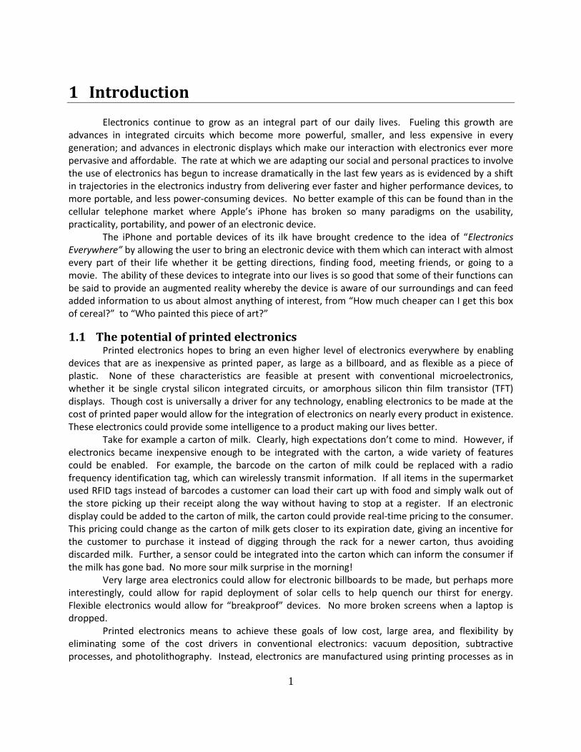
the graphic arts, but with the use of a series of functional materials which can be formulated into inks, and after printing, converted to metals, insulators, and semiconductors. The development of these materials has been a long way in the making, relying on developments in nanoparticle science, conductive polymers, organic semiconductors, and polymer dielectrics, and have allowed for the demonstration of solution processed solar cells, organic light emitting diodes, sensors, and thin film transistors as shown in Figure 1.1. Though these devices are of considerably lower performance than their vacuum deposited or crystalline inorganic counterparts, they offer the potential of being printed, and can thus be integrated into applications where no other technology can be.
Figure 1.1. Materials that have enabled printed thin film transistors.
Aside from the materials, a key component to making the goals of printed electronics a reality is the ability to deposit these materials, en masse, on inexpensive substrates. However, at this point most of the work in printed electronics has revolved around the use of ink-jet printing as a deposition method, and silicon and glass as substrates. Ink-jet provides a great research tool because it uses very small amounts of ink, is a digital process and thus allows for rapid prototyping of different patterns and structures, and has fairly low capital costs. However, it is a serial printing process which therefore results in a very low throughput. Though attempts to use massively scaled ink-jet printers with 1,000 or even 1,000,000 nozzles at a time could dramatically increase this throughput, those attempts have been met with reliability problems, and high cost.
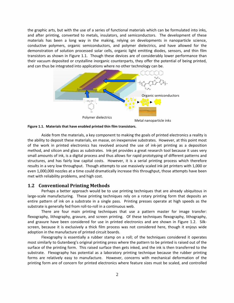
1.2 Conventional Printing Methods Perhaps a better approach would be to use printing techniques that are already ubiquitous in large-scale manufacturing. These printing techniques rely on a rotary printing form that deposits an entire pattern of ink on a substrate in a single pass. Printing presses operate at high speeds as the substrate is generally fed from roll-to-roll in a continuous web. There are four main printing techniques that use a pattern master for image transfer: flexography, lithography, gravure, and screen printing. Of these techniques flexography, lithography, and gravure have been considered for use in printed electronics and are shown in Figure 1.2. Silk-screen, because it is exclusively a thick film process was not considered here, though it enjoys wide adoption in the manufacture of printed circuit boards. Flexography is essentially a rubber stamp on a roll; of the techniques considered it operates most similarly to Gutenberg’s original printing press where the pattern to be printed is raised out of the surface of the printing form. This raised surface then gets inked, and the ink is then transferred to the substrate. Flexography has potential as a laboratory printing technique because the rubber printing forms are relatively easy to manufacture. However, concerns with mechanical deformation of the printing form are of concern for printed electronics where feature sizes must be scaled, and controlled

3
as much as possible. Further the polymer printing form poses limitations on the type of inks that can be printed, as inks with organic solvents can easily cause swelling or deterioration of the form.
Figure 1.2. Conventional printing processes with inset photographs of a flexography roll (top left) and a gravure roll (bottom middle).
Lithography, specifically offset lithography, is one of the most widely used printing techniques, as it used to print the majority of newspapers and short-run periodicals in the world. It makes use of a printing form that is patterned with hydrophobic and hydrophilic regions. The printing form is dampened with water which adheres only on the hydrophilic regions, and then inked with a hydrophobic ink, which adheres only to the hydrophobic regions of the roll. This pattern of water and ink is then transferred to an intermediary offset roll, and then to the substrate where with paper substrates, the water prevents the ink from spreading as it is absorbed by the paper, providing good quality prints. For electronics, the use of two types of fluids to print one pattern poses unwanted constraints on the design of electronic inks, issues with cross-contamination could be difficult to control, and since most substrates for printed electronics are non-absorbent, the benefits of spreading control are minimal. Further offset litho makes use of two patterns transfers, one from the print master to offset roll, and one from the offset roll to the substrate. This extra transfer can lead to added loss of pattern fidelity which is undesirable.
4
The last printing technique discussed is gravure. Gravure, also known as rotogravure, is in some sense the inverse process of flexography. Here patterns are etched into the surface of the printing form, creating ink-holding wells which are filled when the entire roll gets coated in ink. A doctor blade then removes excess ink from the non-patterned areas, and the ink from the wells is transferred from to the substrate. Direct gravure provides the highest resolution and pattern fidelity of these techniques because it uses a metallic printing form which does not suffer from deformation or solvent swelling. Further, ink is transferred directly to the substrate, avoiding the need for a secondary transfer process. Because of the materials used in the printing form, gravure can withstand the highest printing speeds allowing for large numbers of prints in a short time. The downside however, is that gravure rolls are very expensive to pattern, and the patterning process is fairly slow making gravure less ideal for print jobs that vary a lot from day to day. Also, direct gravure is not amenable for printing on solid substrates as mating the printing form and the substrate is impractical, to overcome this, offset gravure must be utilized and a two-transfer method is used, reducing overall resolution.
1.3 Goals In this work gravure has been chosen to develop printing processes for electronics. Though gravure is the most expensive of the techniques discussed, it is the highest resolution, fastest, and most compatible with a variety of materials. The goal in developing these printing processes is to bridge the gap between materials and methods used for ink-jet printing in the laboratory and the materials and methods required to print electronics at an industrial scale. There is little known about how conventional printing processes will perform in printed electronics, and there is potentially a large difference in the materials needed for printing with conventional processes versus ink-jet. As will be shown, there are several technological challenges to enabling printed electronics with conventional printing presses. To begin with, a printing press suitable for new materials development and high resolution printing has not, until now, been developed. Here, such a press is designed, fabricated, and demonstrated. Further, the feature sizes used in graphic arts have not been sufficiently scaled to enable high density, and good performance electronic devices. Here the scalability of gravure for printing metallic lines and dielectrics is shown, giving an indication of the potential to scaling with this technique. Finally, integration issues of multi-level thin film devices have not been well understood, making it difficult to know what printing techniques are best suited for. A printing process for organic thin film transistors has been developed, carefully studying process modules for metals, dielectrics, and insulators separately, and exploring the compatibility between each process to enable high performance devices.
1.4 Background This is not the first attempt at using gravure for purposes of electronics. One of the earliest reports on this was by Mizuno and Okazaki at Dai Nippon Printing, where they demonstrate the use of gravure offset to print the black matrix for color filters in active matrix displays [1]. Soon after, an offset gravure printed resist process was developed for manufacturing amorphous silicon (a-Si:H) TFTs [2]. Both of these reports used an etched glass intaglio to transfer patterns to the offset roller, and achieved feature sizes as small as 10 μm. In 2002 a report on gravure printing functional materials for electronics was made by Gamota where gold nanoparticle inks, polymer dielectrics, and organic semiconductors were combined to fabricate thin film transistors, again using a gravure offset technique [3]. Here minimum feature sizes where 50 μm and due to poor registration capabilities devices used non-overlapping contacts yielding fairly low performance. Soon after, Pudas began studying the ink-transfer process for metallic inks on

5
ceramic substrates [4] using gravure offset, and continued this work demonstrating printed antennas on ceramic substrates[5] and plastic substrates with feature sizes as small as 20 μm [6]. As noted, these early demonstrations used gravure offset instead of direct gravure yet obtained reasonably small patterns on mostly non-flexible substrates as a good indication of the scalability of the gravure printing process. Direct gravure was demonstrated for the fabrication of organic light emitting diodes in 2005 by Tuomikoski [7] and more recently for the deposition of indium tin oxide nanoparticles for transparent electrodes [8]. During the course of research for this work, two other groups have demonstrated the use of direct gravure printing for electronics: the group of Cho in Korea [9], and the group of Hahn in Germany [10]. In their work, these groups demonstrate thin film transistors on flexible substrates using gravure and a combination of other printing techniques. Though they demonstrate some of the earliest circuits fabricated using mass-printing techniques, their performance is somewhat hindered by large feature sizes. This work is complementary in the fact that gravure printed organic thin film transistors are also fabricated as part of the goal of demonstrating gravure’s feasibility for printed electronics, but adds to that with a thorough discussion on the development of a high-resolution gravure printer, and the careful development of high-quality patterned thin film materials that enable devices with significantly better performance than previously demonstrated.
1.5 Organization Thus this thesis is organized in the following manner: Chapter 2 will discuss the gravure printing technique in detail and describe the design of a high-resolution table-top gravure printer suitable for laboratory scale research on printed electronics, as well as the patterning of fine features on gravure cylinders. Chapter 3 will then discuss the issues in printing metallic traces, describing the needs and requirements for these traces in printed circuit boards, interconnects, and contacts to semiconductor devices. Here gravure printing of nanoparticle and organometallic inks will be described along with an understanding of the mechanics of line formation and the scalability of gravure features. Chapter 4 will then discuss gravure printed dielectrics, and the integration of these dielectrics with metal traces to make thin film capacitors. Finally, Chapter 5 will describe the integration of these technologies to make organic thin film transistors, discussing trade-offs in materials selections, printing processes, and device structures.
1.6 Works Cited [1] K. Mizuno, J. J.A.P., Vol. 30, No. 11B (1991) 3313-3317., [2] Y. Mikami, IEEE Trans. Elec. Dev., 41 (1994) 306-314., [3] D. Gamota, Mat. Res. Soc. Symp. Proc. Vol. 725 (2002) P6.3.1-P6.3.6., [4] Pudas, Marko, Hagberg, Juha and Leppavüori, Sepo., "The Absorption Ink Transfer Mechanism of Gravure Offset Printing for Electronic Circuitry." s.l. : IEEE Transactions on Electronics Packaging Manufacturing, 2002, Issue 4, Vol. 25, pp. 335-343. [5] M. Pudas, J. Eur. Cer. Soc., 24 (2004) 2943–2950., [6] M. Pudas, Prog. In Org. Coat., 54 (2005) 310-316., [7] Tuomikoski, M., et al., "Gravure printed optoelectronic thin films for flexible polymer LEDs and microsystems." s.l. : IEEE/LEOS International Conference on Optical MEMS and their Applications, 1-4 August, 2005. pp. 141-142. [8] Puetz, Joerg and Aegerter, Michel., "Direct gravure printing of indium tin oxide nanoparticle patterns on polymer foils." s.l. : Thin Solid Films, 2008. pp. 4495-4501. doi:10.1016/j.tsf.2007.05.086.

6
[9] Cho, Gyoujin., "R2R Printed TFTs and RFID Tags: Demonstration of All Printed 13.56 MHz Operated 1 Bit RFID Tags." Hsinchu, Taiwan : International Symposium on Flexible Electronics and Displays, November 13-14, 2008. [10] Huelber, A.C., "Ring oscillator fabricated completely by means of mass-printing technologies." s.l. : Organic Electronics, 2007, Vol. 8, pp. 480-486.

7
2 Gravure
2.1 Introduction Printing presses have had an enormous impact on our ability to share and communicate ideas, ever since Gutenberg’s first inventions. Today, the vast majority of print material is produced on roll-type printing presses using a variety of techniques including lithography, offset printing, flexography and gravure. Of these techniques, gravure is the least complex, and offers the highest resolution. This has made it an attractive candidate for use in manufacturing printed electronics, where resolution requirements are much higher than those required for publication prints. Using a high throughput process to manufacture integrated circuits has the potential of providing ultra low cost electronics that can have a vast number of new applications, such as electronic paper, smart labels and embedded sensors. All of which aim at providing us with a higher quality of life.
Figure 2.1. The gravure printing process.
2.1.1 Gravure printing fundamentals The gravure printing process uses a metallic roll, also known as the gravure roll, in which the images to be printed have been etched or engraved into its surface. As shown in Figure 2.1, these patterns are filled with ink, and any excess is subsequently wiped off using a blade which is tightly pressed against the roll, the doctor blade. The inked and wiped surface of the roll then comes into
8
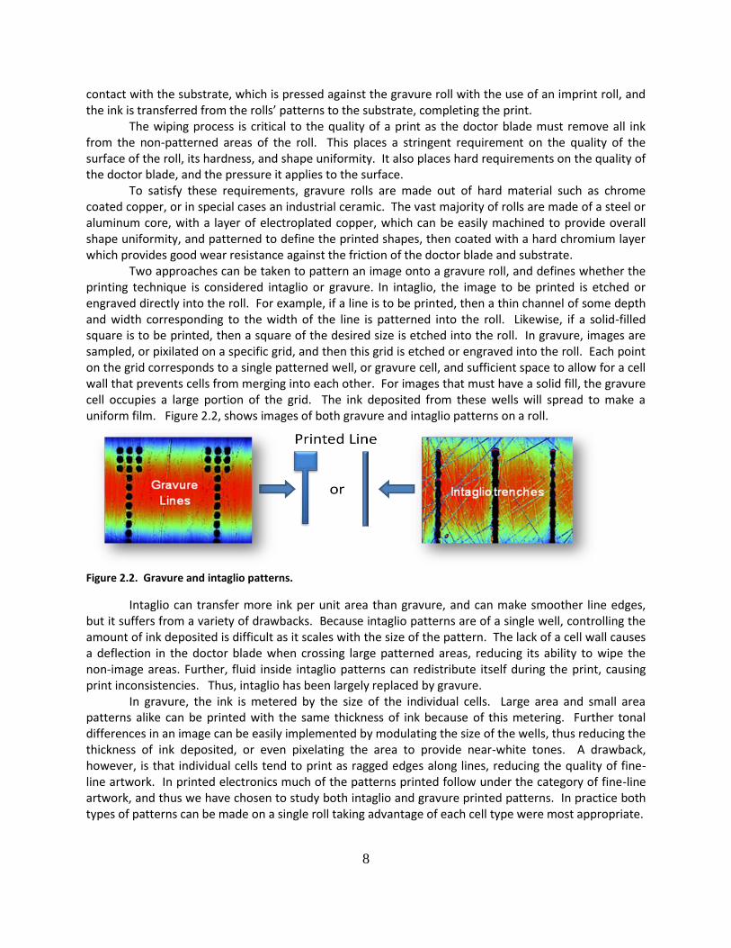
contact with the substrate, which is pressed against the gravure roll with the use of an imprint roll, and the ink is transferred from the rolls’ patterns to the substrate, completing the print. The wiping process is critical to the quality of a print as the doctor blade must remove all ink from the non-patterned areas of the roll. This places a stringent requirement on the quality of the surface of the roll, its hardness, and shape uniformity. It also places hard requirements on the quality of the doctor blade, and the pressure it applies to the surface. To satisfy these requirements, gravure rolls are made out of hard material such as chrome coated copper, or in special cases an industrial ceramic. The vast majority of rolls are made of a steel or aluminum core, with a layer of electroplated copper, which can be easily machined to provide overall shape uniformity, and patterned to define the printed shapes, then coated with a hard chromium layer which provides good wear resistance against the friction of the doctor blade and substrate. Two approaches can be taken to pattern an image onto a gravure roll, and defines whether the printing technique is considered intaglio or gravure. In intaglio, the image to be printed is etched or engraved directly into the roll. For example, if a line is to be printed, then a thin channel of some depth and width corresponding to the width of the line is patterned into the roll. Likewise, if a solid-filled square is to be printed, then a square of the desired size is etched into the roll. In gravure, images are sampled, or pixilated on a specific grid, and then this grid is etched or engraved into the roll. Each point on the grid corresponds to a single patterned well, or gravure cell, and sufficient space to allow for a cell wall that prevents cells from merging into each other. For images that must have a solid fill, the gravure cell occupies a large portion of the grid. The ink deposited from these wells will spread to make a uniform film. Figure 2.2, shows images of both gravure and intaglio patterns on a roll.
Figure 2.2. Gravure and intaglio patterns.
Intaglio can transfer more ink per unit area than gravure, and can make smoother line edges, but it suffers from a variety of drawbacks. Because intaglio patterns are of a single well, controlling the amount of ink deposited is difficult as it scales with the size of the pattern. The lack of a cell wall causes a deflection in the doctor blade when crossing large patterned areas, reducing its ability to wipe the non-image areas. Further, fluid inside intaglio patterns can redistribute itself during the print, causing print inconsistencies. Thus, intaglio has been largely replaced by gravure. In gravure, the ink is metered by the size of the individual cells. Large area and small area patterns alike can be printed with the same thickness of ink because of this metering. Further tonal differences in an image can be easily implemented by modulating the size of the wells, thus reducing the thickness of ink deposited, or even pixelating the area to provide near-white tones. A drawback, however, is that individual cells tend to print as ragged edges along lines, reducing the quality of fine-line artwork. In printed electronics much of the patterns printed follow under the category of fine-line artwork, and thus we have chosen to study both intaglio and gravure printed patterns. In practice both types of patterns can be made on a single roll taking advantage of each cell type were most appropriate.

9
The inks used in gravure can vary quite a bit in formulation and viscosity. Solvent based inks were originally the most popular in the graphic arts, but have fallen out of favor due to environmental concerns. Now most inks for printed media are water based. UV curable inks are also popular because they can be formulated with a small amount of solvents and can provide uniform thick films. Ink viscosities can range from 10 to 500 centiPoise (cP) [1]. Lower viscosity inks are more common in print media such as magazines and books, while higher viscosity inks are found in packaging. Commercial gravure printing presses are large machines that utilize gravure rolls that can be as small as 20 cm wide and 5 cm in diameter, and as big as 3 meters wide and 1.5 meters in diameter. A complete printing press includes a number of gravure stations, each to print a specific color, ink drying or curing stations between each gravure printing station, mechanics for active registration, and wind and unwind for a continuous substrate, or less commonly, send and receive stations for a sheet fed system. All together these presses can be as long as 70 meters, and require an entire warehouse to operate. Thanks to the good mechanical and thermal stability of the gravure roll, these presses can operate at speeds as high as 2,000 m/min, which make gravure, by far the fastest printing technique in use. Due to the high cost of patterning gravure rolls, and speed of the printing systems, gravure is only economically feasible for very large print runs in excess of 500,000 copies.
2.1.2 Table-Top Proof Presses and Laboratory Presses For laboratory use, such as is needed in ink and product development in the graphic arts, two types of presses exist: table-top proof presses and laboratory presses. Because of their smaller size and cost, these presses were considered for use in developing processes for printed electronics.
Figure 2.3. Two proof presses. A K printing proofer (left) and a IGT G1-5 (right).
Proof presses are small machines that are ideal for ink development, and rapid print testing. Two notable machines are a K Printing Proofer by RK Print Coat Instruments, and the G1-5 by IGT, both shown in Figure 2.3. The K Printing Proofer uses a flat ballard shell as the printing form. A ballard shell is a product of a common way of patterning gravure rolls and can thus be easily exchanged with custom patterns by the user. The substrate on this system is wrapped around the imprint roller, and placed on a frame that uses micrometer control to adjust the pressure of the imprint roller, and holds the doctor blade just fore of the substrate. The print is made by moving this frame along the ballard shell, such that the doctor blade inks and wipes the shell before the substrate rolls over it. The IGT G1-5, uses small

10
custom-made gravure rolls, and uses a flat rubber sheet as an imprint roller, with a harder roller behind it that drives the substrate under the roll during the print. Printing pressure is controlled on this printer by a counterweight system. These proof presses are quite inexpensive, and utilize very small amounts of ink (<1mL) per print, which is ideal for printing high-value experimental materials. However, they suffer a few drawbacks. Because of the small size of the printing forms and substrates, these printers only produce results from the few rotations of the gravure roll. In these early stages, ink may have not fully filled all gravure cells, and the printing process may have not reached a steady state condition. Further, these printers are seriously limited by the speed at which they can print. Finally, there are no provisions for registration and thus these printers are only useful for single-layer prints. So called laboratory presses, are much larger machines, which much more closely resemble industrial printing presses. These are web-fed systems, which can have multiple printing units, inline drying and automatic registration feedback Figure 2.4. What distinguishes them from their larger counterparts is mainly the size of the printing form and thus the amount of ink required to operate them. Printing forms on laboratory presses can be as narrow as 10 cm and as wide as 50 cm. Because they are web fed systems, they print continuously and thus achieve steady state printing conditions and allow for many printing variables to be changed on the fly. The problem, however, is that these machines are still quite large for laboratory scale printed electronics, and require at minimum hundreds of milliliters of ink per print.
Figure 2.4. A laboratory scale gravure printing press with two print units, and automatic registration capability.
Neither of these types of presses provides all of the features of a full size gravure press, and neither satisfies the requirement of using very small amounts of ink and allowing for high-precision multi-layer printing. Because of this, a custom laboratory press was built.
2.2 A Laboratory Scale Gravure Printer for Printed Electronics The field of printed electronics is still in development, and thus, the majority of printing work is done at a laboratory level, most commonly with ink-jet printers that provide enormous flexibility and small material volume requirements. However, ink-jet is not a technology that can easily provide for high volume manufacturing, and inks developed for ink-jet do not easily transfer to high volume roll-type processes. In an ideal case, a gravure printing press for printed electronics would combine the small form-factor and low ink usage of a proof press, with the multi-layer registration capability and continuous output of a laboratory press. In terms of resolution and registration, however, such a printer should not
11
be compared to other gravure printers, but to machines currently used for printed electronics and large-area microelectronics, ink-jet printers and photolithography tools, respectively. Ink-jet printers are by far the most widely used in printed electronics. They benefit from being a digital process, giving a lot of flexibility in creating new printing patterns and allowing for real-time pattern changes which are practical for printing on plastic substrates which suffer from large amounts of strain during thermal processing. Ink-jet printers can also print a wide variety of inks including organic and aqueous solvent based inks, UV curable inks, and even molten solders. State-of-the art ink-jet printers use high-precision air bearing stages which can have sub-micron position repeatability and linearity. Ink can be deposited in volumes which range from 100pL to 1pL using widely available micromachined printing cartridges that can print features that range from 100’s of μm to as low as 20 μm. Improvements in resolution have been demonstrated by the use of electrohydrodynamic jetting which can deposit femtoliter drop volumes, though these systems are still in early development [2][3]. Despite good machine accuracy and small drop volumes, ink-jet suffers from a large variability in drop directionality, limiting its position accuracy to 5 – 10 μm. For large-area electronics, the main products are a-Si:H TFTs for liquid crystal displays, which are manufactured by photolithography. These photolithography tools are 1:1 projection steppers, which have a registration capability of 0.5 μm and a can pattern features as small as 2.5 μm over areas as large as 2.5m x 3m.
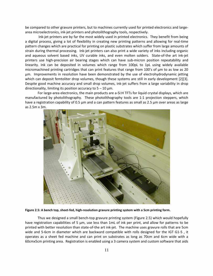
Figure 2.5: A bench top, sheet-fed, high-resolution gravure printing system with a 5cm printing form.
Thus we designed a small bench-top gravure printing system (Figure 2.5) which would hopefully have registration capabilities of 5 μm, use less than 1mL of ink per print, and allow for patterns to be printed with better resolution than state-of-the art ink-jet. The machine uses gravure rolls that are 5cm wide and 5-6cm in diameter which are backward compatible with rolls designed for the IGT G1-5 , it operates as a sheet fed machine and can print on substrates as long as 70cm and 6cm wide with a 60cmx5cm printing area. Registration is enabled using a 3 camera system and custom software that aids
12
the user in aligning fiducial marks on the roll with those on the substrate. To improve registration and eliminate errors due to environmental vibrations the system was mounted on an air-cushion table. It was built with a heavy steel frame to avoid any mechanical deflections and minimize the effects of thermal expansion. A Parker-Hafnin 404LXR linear motor provides the driving force to move the substrate through the printing process at speeds up to 2 m/s. To realize good registration accuracy, principles of precision machine design (error mapping and error budget) were used to describe and analyze the registration capability of this printing machine in order to determine and quantify the major sources of alignment error, and determine possible solutions to these errors. A description of the alignment process will be given followed by an experimental measurement of its printing errors. With this in mind, we take on the task of building an error map and error budget for the machine [4]. We first determine the thermal errors from a coupled thermal-structural analysis of the machine using finite element simulations, we then build kinematic model of the machine using homogeneous transformation matrices (HTMs). Using these HTMs we combine the thermal errors with errors coming from a variety of other sources such as the motors and stages which move the machine components during a print, and we calculate the total expected alignment error of the machine, using HTMs to quantify the impact of each error source. Finally, we propose and implement series of improvements to the printing system, using the knowledge gleaned from our analysis.
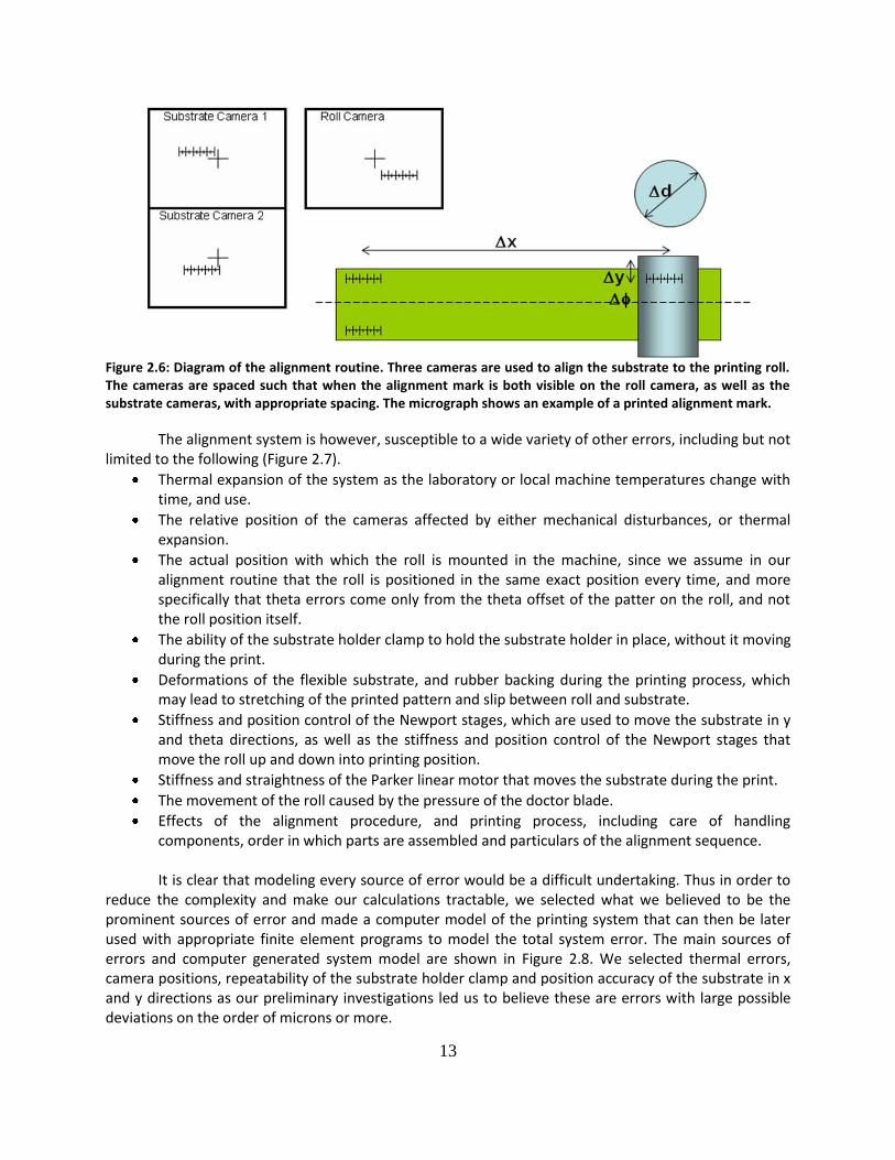
2.2.1 Alignment Process and Sources of Error The gravure printing system shown in Figure 2.5 is a sheet fed system which operates as follows: A plastic sheet (a.k.a. substrate) is mounted on the black sample holder with a rubber backing using two clamps. The sample holder is then mounted onto a larger base plate (a.k.a. top plate) and two high precision double-row ball bearing Newport stages through a clamp. The substrate is then aligned to the gravure roll using three Navitar microscopes, a small piece of alignment software, the aforementioned Newport stages to provide motion in the y and theta directions, as well as a Parker-Hafnin linear motor which moves the stage in the printing direction x. Once the alignment has been done with the roll sitting slightly above the substrate, it is lowered onto the substrate and loaded with a spring-based compression system to a weight of approximately 10kg and the alignment is re-checked. If the alignment is good, a doctor blade is placed against the roll, the roll is inked, then the substrate is moved under the roll (which rotates) using the Parker linear motor to transfer the ink from the roll to the substrate. The alignment routine can be described using Figure 2.6. The substrate is placed under the roll such that the alignment marks on the substrate are a distance x away from the axis of the roll. This
distance should be 1.5 times the circumference of the roll, or 3/2 d, where d is the diameter of the roll. This will ensure that the alignment mark, which is seen at the top of the roll through the roll camera, will roll directly on top of the alignment marks shown in substrate camera 1. A second alignment mark on the roll will print over the mark shown in camera 2, as long as the relative rotation of the substrate is adjusted by properly relating alignment marks on substrate camera 1 to substrate camera 2. Thus, the distance between the substrate cameras and the roll camera must also be 1.5 times the circumference of the roll to ensure the alignment marks are centered exactly in the camera window. However, since
the diameter of each roll is slightly different, there is a deviation of roll diameter d, which leads to a
need to offset the alignment marks by a distance x = 3/2 d. The pattern on the roll may also not be aligned exactly in y and theta direction between roll and roll. We thus use a software program to keep
calibrated values of d and theta, and thus corresponding values of x and y required to align a variety of different rolls to each other.
13
Figure 2.6: Diagram of the alignment routine. Three cameras are used to align the substrate to the printing roll. The cameras are spaced such that when the alignment mark is both visible on the roll camera, as well as the substrate cameras, with appropriate spacing. The micrograph shows an example of a printed alignment mark.
The alignment system is however, susceptible to a wide variety of other errors, including but not limited to the following (Figure 2.7).
Thermal expansion of the system as the laboratory or local machine temperatures change with time, and use.
The relative position of the cameras affected by either mechanical disturbances, or thermal expansion.
The actual position with which the roll is mounted in the machine, since we assume in our alignment routine that the roll is positioned in the same exact position every time, and more specifically that theta errors come only from the theta offset of the patter on the roll, and not the roll position itself.
The ability of the substrate holder clamp to hold the substrate holder in place, without it moving during the print.
Deformations of the flexible substrate, and rubber backing during the printing process, which may lead to stretching of the printed pattern and slip between roll and substrate.
Stiffness and position control of the Newport stages, which are used to move the substrate in y and theta directions, as well as the stiffness and position control of the Newport stages that move the roll up and down into printing position.
Stiffness and straightness of the Parker linear motor that moves the substrate during the print.
The movement of the roll caused by the pressure of the doctor blade.
Effects of the alignment procedure, and printing process, including care of handling components, order in which parts are assembled and particulars of the alignment sequence.
It is clear that modeling every source of error would be a difficult undertaking. Thus in order to reduce the complexity and make our calculations tractable, we selected what we believed to be the prominent sources of error and made a computer model of the printing system that can then be later used with appropriate finite element programs to model the total system error. The main sources of errors and computer generated system model are shown in Figure 2.8. We selected thermal errors, camera positions, repeatability of the substrate holder clamp and position accuracy of the substrate in x and y directions as our preliminary investigations led us to believe these are errors with large possible deviations on the order of microns or more.

14
Figure 2.7: Gravure printing system and a range of possible sources of error.
Figure 2.8: Computer model of gravure printing system and predicted major sources of error.
2.2.2 Experimental Position Repeatability and Alignment Accuracy As built, this gravure printing system was intended to afford up to 5 m alignment accuracy. However, we quickly determined that the practical alignment accuracy of the machine was, in fact, much worse. In order to isolate the major sources of error a few repeatability experiments were carried
out on the machine. Using an electronic Mitutoyo indicator with a 1 m resolution, we quickly assessed that a major source of error came from positional repeatability of the substrate. This could be due to the
X-position
control
Y Straightness
Stage Stiffness
z
y
x
z
y
x
Doctor blade
force
Camera position
x,y,z and
3 cameras
Camera
relative positions
Kinematic
Clamp
Stage Stiffness
Substrate
Holder
Roll Position
x, y, ?
Plastic
and Rubber
Deformations
Thermal
Expansion!
Process
Effects!
X-position
control
Y Straightness
z
y
x
z
y
x
Camera position
x, y, z and
3 cameras
Camera
relative positions
Kinematic Clamp
Thermal
Expansion!

15
repeatability of the substrate holder clamp, which was designed to couple the substrate holder to the Newport stages on the base plate, while still affording movement of the substrate holder in y and theta directions. It could also be due to the repeatability of the parker stage, which should move the substrate straight under the roller and back to the same position after the print.
2.2.2.1 Substrate holder Clamp Repeatability In order to assess the repeatability of the substrate holder clamp, the substrate was placed on the base plate and clamp, and its position in the x and y direction was measured with the electronic indicator. The substrate holder was then removed and the process repeated 50 times, taking measurements in x and y at both extremes of the substrate holder, centered about the contact point of each clamp (one at the front of the substrate holder, and one at the back). The data collected is
presented in Figure 2.9. Clearly, repeatability for both clamps is worse than 5 m, especially in the y
direction where the error is 30 m for the front clamp and 20 m for the back clamp.
Figure 2.9: Position repeatability of substrate holder clamps. For the front clamp x= 5 m, y= 30 m, for the
back clamp x= 7 m, y= 20 m.
2.2.2.2 Base Plate Repeatability We also tested the repeatability of the base plate (onto which the substrate holder is placed) and parker motor using a similar technique. We mounted a small photo-lithographically patterned silicon wafer onto the sample holder using a double sided 3M brand tape, and moved the stage back and forth 500mm 50 times measuring the position of a small alignment mark on the wafer, in the field of view of the camera.
The resolution of the camera was calibrated to be 0.62 m/pixel with an 860×640 pixel display. We used an onscreen cursor with a pixel position-tracking program to align a crosshair cursor to the center of a crosshair alignment mark that was patterned onto the wafer with a 5um line width. This allowed for easy centering as the eye can easily catch the symmetry of light shining on the dark cursor crosshair from the shiny gold alignment mark. Surprisingly, after measuring the position of the crosshair after 500mm back-and-forth movements using a velocity of 20cm/s and an acceleration of 40 m/s2, we found that the positional error
was only 0.36 m in the y-direction (perpendicular to the direction of motion) and 1.63 m along the x-direction, the direction of motion. The two graphs presented below indicate the there is indeed more control in the y direction that in the x (Figure 2.10) but even more importantly, there seems to be a
16
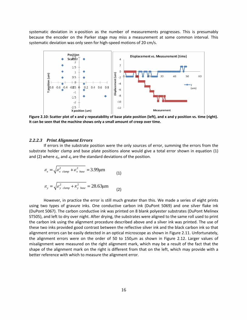
systematic deviation in x-position as the number of measurements progresses. This is presumably because the encoder on the Parker stage may miss a measurement at some common interval. This systematic deviation was only seen for high-speed motions of 20 cm/s.
Figure 2.10: Scatter plot of x and y repeatability of base plate position (left), and x and y position vs. time (right). It can be seen that the machine shows only a small amount of creep over time.
2.2.2.3 Print Alignment Errors If errors in the substrate position were the only sources of error, summing the errors from the substrate holder clamp and base plate positions alone would give a total error shown in equation (1)
and (2) where x, and y are the standard deviations of the position.
2 2 3.99μmx x clamp x base (1)
2 2 28.63μmy y clamp y base (2)
However, in practice the error is still much greater than this. We made a series of eight prints using two types of gravure inks. One conductive carbon ink (DuPont 5069) and one silver flake ink (DuPont 5067). The carbon conductive ink was printed on 8 blank polyester substrates (DuPont Melinex ST505), and left to dry over night. After drying, the substrates were aligned to the same roll used to print the carbon ink using the alignment procedure described above and a silver ink was printed. The use of these two inks provided good contrast between the reflective silver ink and the black carbon ink so that alignment errors can be easily detected in an optical microscope as shown in Figure 2.11. Unfortunately,
the alignment errors were on the order of 50 to 150 m as shown in Figure 2.12. Larger values of misalignment were measured on the right alignment mark, which may be a result of the fact that the shape of the alignment mark on the right is different from that on the left, which may provide with a better reference with which to measure the alignment error.
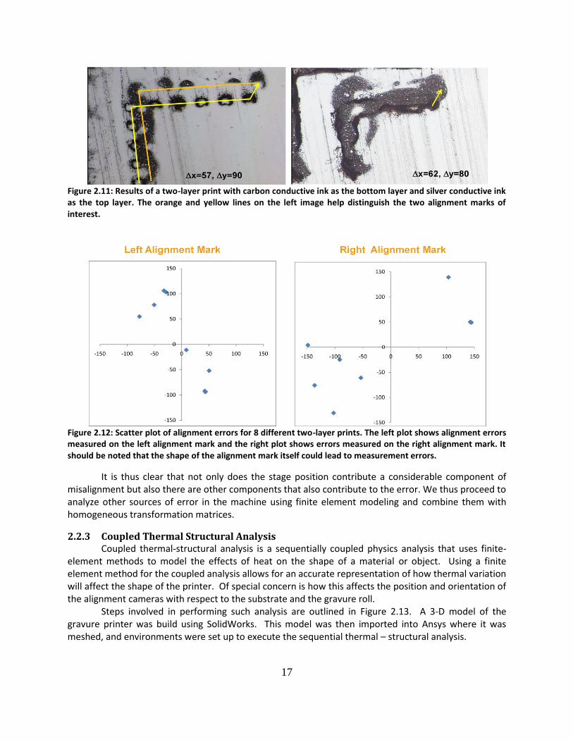
17
Figure 2.11: Results of a two-layer print with carbon conductive ink as the bottom layer and silver conductive ink as the top layer. The orange and yellow lines on the left image help distinguish the two alignment marks of interest.
Figure 2.12: Scatter plot of alignment errors for 8 different two-layer prints. The left plot shows alignment errors measured on the left alignment mark and the right plot shows errors measured on the right alignment mark. It should be noted that the shape of the alignment mark itself could lead to measurement errors.
It is thus clear that not only does the stage position contribute a considerable component of misalignment but also there are other components that also contribute to the error. We thus proceed to analyze other sources of error in the machine using finite element modeling and combine them with homogeneous transformation matrices.
2.2.3 Coupled Thermal Structural Analysis Coupled thermal-structural analysis is a sequentially coupled physics analysis that uses finite-element methods to model the effects of heat on the shape of a material or object. Using a finite element method for the coupled analysis allows for an accurate representation of how thermal variation will affect the shape of the printer. Of special concern is how this affects the position and orientation of the alignment cameras with respect to the substrate and the gravure roll. Steps involved in performing such analysis are outlined in Figure 2.13. A 3-D model of the gravure printer was build using SolidWorks. This model was then imported into Ansys where it was meshed, and environments were set up to execute the sequential thermal – structural analysis.
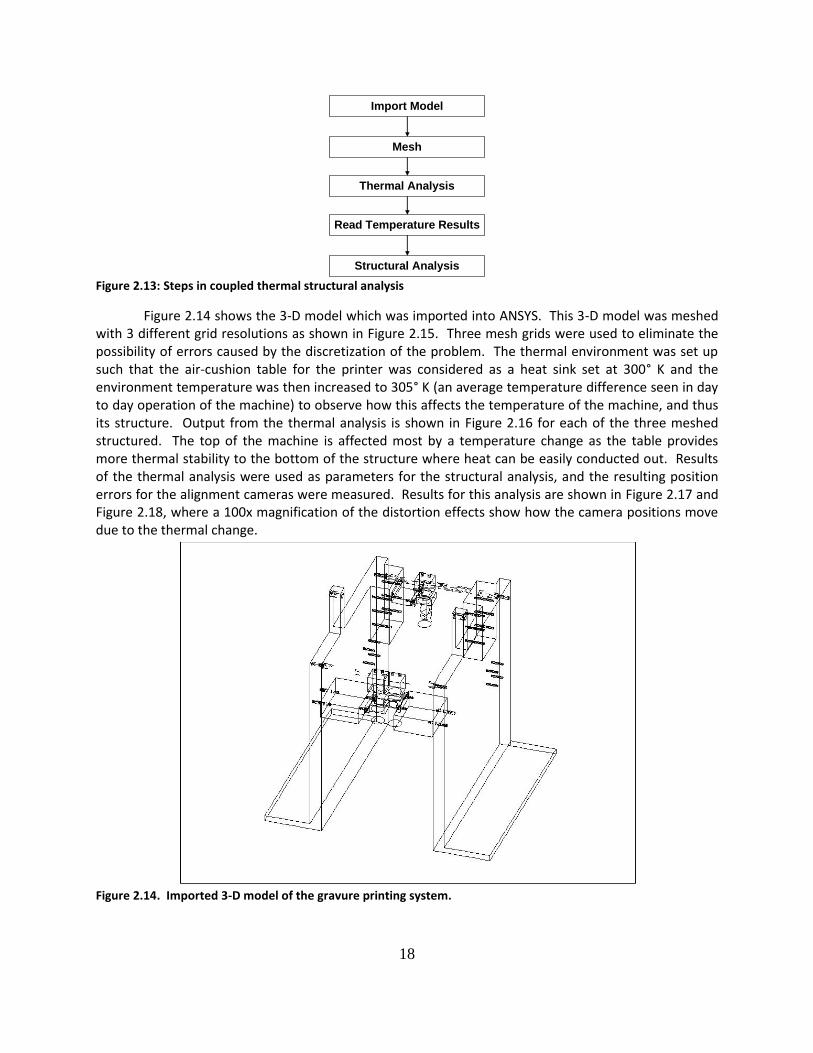
18
Figure 2.13: Steps in coupled thermal structural analysis
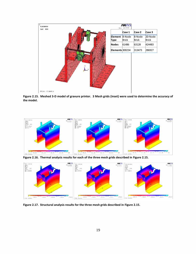
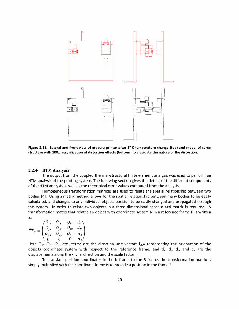
Figure 2.14 shows the 3-D model which was imported into ANSYS. This 3-D model was meshed with 3 different grid resolutions as shown in Figure 2.15. Three mesh grids were used to eliminate the possibility of errors caused by the discretization of the problem. The thermal environment was set up such that the air-cushion table for the printer was considered as a heat sink set at 300° K and the environment temperature was then increased to 305° K (an average temperature difference seen in day to day operation of the machine) to observe how this affects the temperature of the machine, and thus its structure. Output from the thermal analysis is shown in Figure 2.16 for each of the three meshed structured. The top of the machine is affected most by a temperature change as the table provides more thermal stability to the bottom of the structure where heat can be easily conducted out. Results of the thermal analysis were used as parameters for the structural analysis, and the resulting position errors for the alignment cameras were measured. Results for this analysis are shown in Figure 2.17 and Figure 2.18, where a 100x magnification of the distortion effects show how the camera positions move due to the thermal change.
Figure 2.14. Imported 3-D model of the gravure printing system.
Mesh
Import Model
Thermal Analysis
Structural Analysis
Read Temperature Results
19
Figure 2.15. Meshed 3-D model of gravure printer. 3 Mesh grids (inset) were used to determine the accuracy of the model.
Figure 2.16. Thermal analysis results for each of the three mesh grids described in Figure 2.15.
Figure 2.17. Structural analysis results for the three mesh grids described in Figure 2.15.
Case 1 Case 2 Case 3
Element Type
8-Node Brick
8-Node Brick
20-Node Brick
Nodes 61486 63128 424483
Elements 300234 313473 286927
20
Figure 2.18. Lateral and front view of gravure printer after 5° C temperature change (top) and model of same structure with 100x magnification of distortion effects (bottom) to elucidate the nature of the distortion.
2.2.4 HTM Analysis The output from the coupled thermal-structural finite element analysis was used to perform an HTM analysis of the printing system. The following section gives the details of the different components of the HTM analysis as well as the theoretical error values computed from the analysis. Homogeneous transformation matrices are used to relate the spatial relationship between two bodies [4]. Using a matrix method allows for the spatial relationship between many bodies to be easily calculated, and changes to any individual objects position to be easily changed and propagated through the system. In order to relate two objects in a three dimensional space a 4x4 matrix is required. A transformation matrix that relates an object with coordinate system N in a reference frame R is written as
.
Here Oix, Oiy, Oiz, etc., terms are the direction unit vectors i,j,k representing the orientation of the objects coordinate system with respect to the reference frame, and dx, dy, dz, and ds are the displacements along the x, y, z, direction and the scale factor. To translate position coordinates in the N frame to the R frame, the transformation matrix is simply multiplied with the coordinate frame N to provide a position in the frame R
21
.
Using this method, the transformation matrices can be multiplied to relate the position of one object to another, through any number of intermediary objects or frames
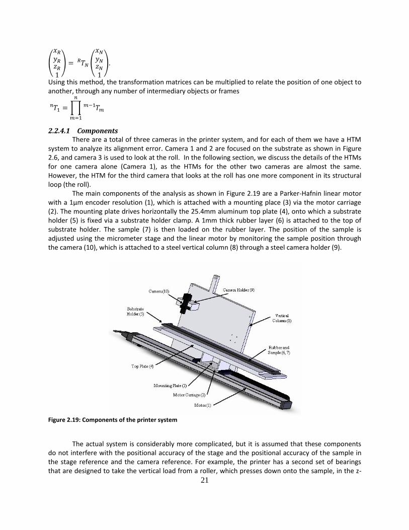
2.2.4.1 Components There are a total of three cameras in the printer system, and for each of them we have a HTM system to analyze its alignment error. Camera 1 and 2 are focused on the substrate as shown in Figure 2.6, and camera 3 is used to look at the roll. In the following section, we discuss the details of the HTMs for one camera alone (Camera 1), as the HTMs for the other two cameras are almost the same. However, the HTM for the third camera that looks at the roll has one more component in its structural loop (the roll). The main components of the analysis as shown in Figure 2.19 are a Parker-Hafnin linear motor with a 1μm encoder resolution (1), which is attached with a mounting place (3) via the motor carriage (2). The mounting plate drives horizontally the 25.4mm aluminum top plate (4), onto which a substrate holder (5) is fixed via a substrate holder clamp. A 1mm thick rubber layer (6) is attached to the top of substrate holder. The sample (7) is then loaded on the rubber layer. The position of the sample is adjusted using the micrometer stage and the linear motor by monitoring the sample position through the camera (10), which is attached to a steel vertical column (8) through a steel camera holder (9).
Figure 2.19: Components of the printer system
The actual system is considerably more complicated, but it is assumed that these components do not interfere with the positional accuracy of the stage and the positional accuracy of the sample in the stage reference and the camera reference. For example, the printer has a second set of bearings that are designed to take the vertical load from a roller, which presses down onto the sample, in the z-

22
direction. Since we are concerned only with x and y displacements for this analysis these components are orthogonal, and thus do not interfere. The structural loop for this camera is shown in Figure 2.20.
Figure 2.20: Structural loop for a single camera.
Figure 2.21 schematically shows the coordinate system and the origins (reference points) for each component in the structural loop.
Figure 2.21: Coordinate systems and reference points.
2.2.4.2 HTMs for Camera 1 The systematic analysis of the alignment errors for camera 1 is listed in
Table 2.1. The values of motion, offset, and positional errors caused by thermal expansion are also specified in the table. The values of other errors are calculated in the next section.
0 1 2 3 4 5
8 9 10
6 7
0 (Ground )
1
8
3
4
5
9
10
Y
Z
X
2
6
7
Reference Point
23
Table 2.1: Analysis of alignment errors for camera 1
Component Motion Offset Positional error Roll/Pitch/Yaw
0→1 Z1 (44.65mm)
1→2 x (314.17mm) Z2 (15.35mm) δx2 Yaw: εz2
2→3 Z3 (76.2mm)
3→4 Z4 (25.4mm)
4→5 Z5 (6.35mm) Yaw: εz5
5→6 Z6 (1mm) δz6
6→7 Z7 (0.5mm) δx7, δy7, δz7 Yaw: εz7
0→8 Y8 (106mm)
8→9
Z9 (291.48mm)
δx9 (-7.78 μm) δy9 (3.68 μm) δz9 (5.21 μm) (due to thermal expansions)
9→10
Y10 (-106mm) Z10 (-122.03mm)
δx10 (0.92 μm) δy10 (-3.71 μm) δz10 (2.44 μm) (due to thermal expansions)
Yaw: εx10
(-89.6 rad) Yaw: εy10
(-20.3 rad)
Based on this table, we can get the HTMs for camera 1 as below.
0
1
1
1 0 0 0
0 1 0 0
0 0 1
0 0 0 1
TZ
2 2
21
2
2
1 0
1 0 0
0 0 1
0 0 0 1
z x
z
x
TZ
2
3
3
1 0 0 0
0 1 0 0
0 0 1
0 0 0 1
TZ
3
4
4
1 0 0 0
0 1 0 0
0 0 1
0 0 0 1
TZ
5
54
5
5
1 0 0
1 0 0
0 0 1
0 0 0 1
z
zT
Z
5
6
6 6
1 0 0 0
0 1 0 0
0 0 1
0 0 0 1
z
TZ
7 7
7 76
7
7 7
1 0
1 0
0 0 1
0 0 0 1
z x
z y
z
TZ
80
8
1 0 0 0
0 1 0
0 0 1 0
0 0 0 1
YT
24
9
98
9
9 9
1 0 0
0 1 0
0 0 1
0 0 0 1
x
y
z
TZ
10 10
10 10 109
10
10 10 10 10
1 0
0 1
1
0 0 0 1
y x
x y
y x z
YT
Z
2.2.4.3 HTMs for Camera 2 The HTM analysis for camera 2 is almost the same as that for camera 1, except that the camera height and the thermal expansion are different since the two camera systems are not symmetric. Table 2.2: Analysis of alignment errors for camera 2
Component Motion Offset Positional error Roll/Pitch/Yaw
0→1 Z1 (44.65mm)
1→2 x (314.17mm) Z2 (15.35mm) δx2 Yaw: εz2
2→3 Z3 (76.2mm)
3→4 Z4 (25.4mm)
4→5 Z5 (6.35mm) Yaw: εz5
5→6 Z6 (1mm) δz6
6→7 Z7 (0.5mm) δx7, δy7, δz7 Yaw: εz7
0→8 Y8 (-106mm)
8→9 Z9 (310.53mm)
δx9 (-6.91 μm) δy9 (-3.80 μm) δz9 (5.74 μm) (due to thermal expansions)
9→10 Y10 (106mm) Z10 (-141.08mm)
δx10 (-0.27 μm) δy10 (3.28 μm) δz10 (2.99 μm) (due to thermal expansions)
Yaw: εx10
(-60.6 rad) Yaw: εy10
(-19.7 rad)
0
1
1
1 0 0 0
0 1 0 0
0 0 1
0 0 0 1
TZ
2 2
21
2
2
1 0
1 0 0
0 0 1
0 0 0 1
z x
z
x
TZ
2
3
3
1 0 0 0
0 1 0 0
0 0 1
0 0 0 1
TZ
3
4
4
1 0 0 0
0 1 0 0
0 0 1
0 0 0 1
TZ
5
54
5
5
1 0 0
1 0 0
0 0 1
0 0 0 1
z
zT
Z
5
6
6 6
1 0 0 0
0 1 0 0
0 0 1
0 0 0 1
z
TZ
25
7 7
7 76
7
7 7
1 0
1 0
0 0 1
0 0 0 1
z x
z y
z
TZ
80
8
1 0 0 0
0 1 0
0 0 1 0
0 0 0 1
YT
9
98
9
9 9
1 0 0
0 1 0
0 0 1
0 0 0 1
x
y
z
TZ
10 10
10 10 109
10
10 10 10 10
1 0
0 1
1
0 0 0 1
y x
x y
y x z
YT
Z
2.2.4.4 HTMs for camera 3 Compared to camera 1 and camera 2, the structural loop of camera 3 includes one more component, which is the roll. The structural loop for camera 3 is shown in Figure 2.22 and the corresponding analysis is listed in Table 2.3.
Figure 2.22: Structural loop for camera 3.
Table 2.3: Analysis of alignment errors for camera 3
Component Motion Offset Positional error Roll/Pitch/Yaw
0→1 Z1 (44.65mm)
1→2 x (314.17mm) Z2 (15.35mm) δx2 Yaw: εz2
2→3 Z3 (76.2mm)
3→4 Z4 (25.4mm)
4→5 Z5 (6.35mm) Yaw: εz5
5→6 Z6 (1mm) δz6
6→7 Z7 (0.5mm) δx7, δy7, δz7 Yaw: εz7
7→8 Z8 (66.5mm) δz8 Yaw: εz8
0→9 Y9 (106mm)
9→10 Z10 (374.03mm) δx10 (6.31 μm) δy10 (4.80 μm) δz10 (12.44 μm)
8
0 (Ground)
1
9
3
4
5
10
11
Y
Z
X
2
6
7
Reference Point

26
(due to thermal expansions)
10→11 Y11 (-106mm) Z11 (-138.08mm)
δx11 (1.48 μm) δy11 (-3.47 μm) δz11 (0.13 μm) (due to thermal expansions)
Yaw: εx11
(-108.4 rad) Yaw: εy11
(-26.3 rad)
The HTMs calculated for camera 3 are given below.
0
1
1
1 0 0 0
0 1 0 0
0 0 1
0 0 0 1
TZ
2 2
21
2
2
1 0
1 0 0
0 0 1
0 0 0 1
z x
z
x
TZ
2
3
3
1 0 0 0
0 1 0 0
0 0 1
0 0 0 1
TZ
3
4
4
1 0 0 0
0 1 0 0
0 0 1
0 0 0 1
TZ
5
54
5
5
1 0 0
1 0 0
0 0 1
0 0 0 1
z
zT
Z
5
6
6 6
1 0 0 0
0 1 0 0
0 0 1
0 0 0 1
z
TZ
7 7
7 76
7
7 7
1 0
1 0
0 0 1
0 0 0 1
z x
z y
z
TZ
8
87
8
8 8
1 0 0
1 0 0
0 0 1
0 0 0 1
z
z
z
TZ
90
9
1 0 0 0
0 1 0
0 0 1 0
0 0 0 1
YT
10
109
10
10 10
1 0 0
0 1 0
0 0 1
0 0 0 1
x
y
z
TZ
11 11
11 11 1110
11
11 11 11 11
1 0
0 1
1
0 0 0 1
y x
x y
y x z
YT
Z
2.2.4.5 Calculated Error Components It is assumed that the travel of the motor in general operation is 314.17 mm. From the experimentally measured data for the 404LXR linear motor, the static x and y-directional errors are 3.83
and 0.95 m, respectively.
Also for a 314.17 mm travel, a straight-line accuracy of 17 m is expected; and hence the angle for the distortion is calculated as shown in equation (3).
27
31 3
2
17 10tan 3.247 10
300z
mmrad
mm (3)
For the sample holder, the sensitivity of the differential micrometer used for the measurement
is 0.1 m. Since the distance to the pivot bolt (pin hole) is 29.527mm, the angle of distortion due to the worst case of error on the micrometer is given by equation (4).
31 4
5
0.1 10tan 1.940 10
29.5278z
mmrad
mm (4)
Assuming that the rubber is tightly stuck on the sample holder, there is no linear and rotational error in component 6. In other words, δx6, δy6, and εz6 are taken to be zero. The error on the sample substrate is obtained from the above experimental measurements. For Camera 1, δx7, δy7 and εz7 are 3.658, 28.63 um, and 1.444 rad, respectively. For Camera 2, 3.658, 6.610 um, and 1.065 rad, and for Camera 3, 21.33, 8.085 um, and 0.362 rad, respectively The equation of the change of length due to thermal expansion is based on the equation given by
TLL However, heat expansion occurs through 3 dimensions; therefore, all six degree errors can be involved. The numerical values for each component were obtained from the FEM analysis.
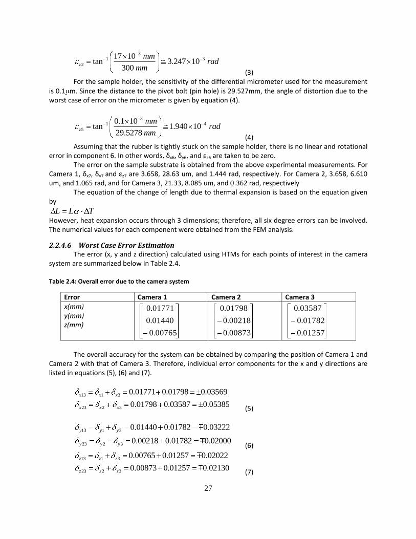
2.2.4.6 Worst Case Error Estimation The error (x, y and z direction) calculated using HTMs for each points of interest in the camera system are summarized below in Table 2.4. Table 2.4: Overall error due to the camera system
Error Camera 1 Camera 2 Camera 3
x(mm) y(mm) z(mm)
The overall accuracy for the system can be obtained by comparing the position of Camera 1 and Camera 2 with that of Camera 3. Therefore, individual error components for the x and y directions are listed in equations (5), (6) and (7).
13 1 3
23 2 3
0.01771 0.01798 0.03569
0.01798 0.03587 0.05385
x x x
x x x (5)
13 1 3
23 2 3
0.01440 0.01782 0.03222
0.00218 0.01782 0.02000
y y y
y y y (6)
13 1 3
23 2 3
0.00765 0.01257 0.02022
0.00873 0.01257 0.02130
z z z
z z z (7)
00765.0
01440.0
01771.0
00873.0
00218.0
01798.0
01257.0
01782.0
03587.0

28
Table 2.5: Summary of errors through the camera system to the substrate
Camera 3 1 3 2
x 35.69 μm 53.85 μm
y 32.22 μm 20.00 μm
Z 20.22 μm 21.30 μm
2.2.5 Discussion As can be seen from Table 2.5, the errors calculated using the experimental values of substrate position error, and the effects of thermal expansion from finite element modeling are considerable, yet smaller than those errors measured experimentally. Qualitatively, the errors from thermal expansion were on the order of 10 μm , while δx7, δy7, the positional errors of the substrate were on the order of 30 μm , thus the calculated errors seem to be reasonable given our assumptions. However, since measured alignment errors in practice on the order of 100 μm, we must assume that other sources of error play significant roles in the total error of the system. It is clear that improving positional errors from the substrate and improving the temperature control of the room can eliminate up to half of the error currently seen. Some simple improvements to our model can perhaps point to other sources of error. For example, we did not consider the thermal expansion of the roll as part of our analysis. This could lead to an increase in all three components of error. We also have not calculated the stiffness of the Newport stages, which will cause motion during the acceleration of the substrate. There may also be a series of procedural improvements which may be significant. For example, due to the confined space of the apparatus the cameras are constantly at a risk of being shifted (bumped) during operation, this may lead to offsets of camera position which cannot be easily modeled. An improved mounting brace, could prevent this type of impact. Further, the temperature of the roll itself is subject to a variety of thermal changes, beyond those of the room, most importantly because the roll is subjected to an ultrasonic cleaning between each printing run. This may cause temperature increases of up to 15°C. The use of a reference sample, could help check or calibrate the camera position before each run, while the use of some thermocouple thermometers, could either allow the alignment program to adjust for alignment offsets due to thermal variations, or allow the operator to ensure the appropriate roll temperature is reached before it is used.
2.2.6 Improvements Our error budget shows that as built the machine has a registration limit of +/- 54 μm in the x or print direction and +/- 20 μm in the y direction, despite being designed to achieve an alignment accuracy of 5 μm. We have found that a poor substrate clamp design and poor thermal control in both the camera positioning and the motor can be accountable for a large portion of this error. To improve the registration capability of the system, a better substrate holder clamp was designed, electronic compensation for linear motor errors was implemented, and a printing protocol was established that would minimize the thermal errors of the machine. These improvements shall be described here.
2.2.6.1 Kinematic Clamp Design for Substrate Holder Clamp The substrate holder clamp was found to add +/- 20 μm of error in the y-direction and +/- 5 μm error in the x-direction. The choice of components and the clamps design are a big reason for this error. The clamp was designed to hold the substrate holder perfectly in place once, locked, but to allow for precision y, and θ control of the substrate (Figure 2.23). In the original design two Newport
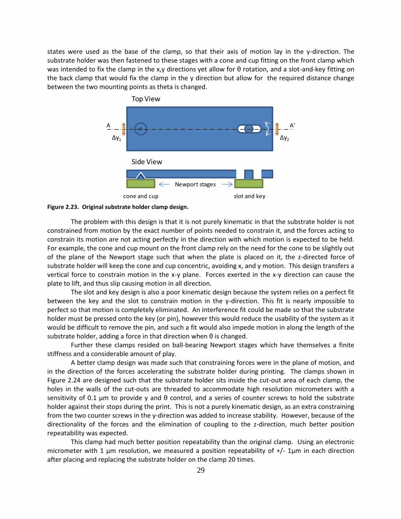
29
states were used as the base of the clamp, so that their axis of motion lay in the y-direction. The substrate holder was then fastened to these stages with a cone and cup fitting on the front clamp which was intended to fix the clamp in the x,y directions yet allow for θ rotation, and a slot-and-key fitting on the back clamp that would fix the clamp in the y direction but allow for the required distance change between the two mounting points as theta is changed.
Figure 2.23. Original substrate holder clamp design.
The problem with this design is that it is not purely kinematic in that the substrate holder is not constrained from motion by the exact number of points needed to constrain it, and the forces acting to constrain its motion are not acting perfectly in the direction with which motion is expected to be held. For example, the cone and cup mount on the front clamp rely on the need for the cone to be slightly out of the plane of the Newport stage such that when the plate is placed on it, the z-directed force of substrate holder will keep the cone and cup concentric, avoiding x, and y motion. This design transfers a vertical force to constrain motion in the x-y plane. Forces exerted in the x-y direction can cause the plate to lift, and thus slip causing motion in all direction. The slot and key design is also a poor kinematic design because the system relies on a perfect fit between the key and the slot to constrain motion in the y-direction. This fit is nearly impossible to perfect so that motion is completely eliminated. An interference fit could be made so that the substrate holder must be pressed onto the key (or pin), however this would reduce the usability of the system as it would be difficult to remove the pin, and such a fit would also impede motion in along the length of the substrate holder, adding a force in that direction when θ is changed. Further these clamps resided on ball-bearing Newport stages which have themselves a finite stiffness and a considerable amount of play. A better clamp design was made such that constraining forces were in the plane of motion, and in the direction of the forces accelerating the substrate holder during printing. The clamps shown in Figure 2.24 are designed such that the substrate holder sits inside the cut-out area of each clamp, the holes in the walls of the cut-outs are threaded to accommodate high resolution micrometers with a sensitivity of 0.1 μm to provide y and θ control, and a series of counter screws to hold the substrate holder against their stops during the print. This is not a purely kinematic design, as an extra constraining from the two counter screws in the y-direction was added to increase stability. However, because of the directionality of the forces and the elimination of coupling to the z-direction, much better position repeatability was expected. This clamp had much better position repeatability than the original clamp. Using an electronic micrometer with 1 μm resolution, we measured a position repeatability of +/- 1μm in each direction after placing and replacing the substrate holder on the clamp 20 times.
Top View
Side View
A A’
cone and cup slot and key
∆y2∆y1
Newport stages
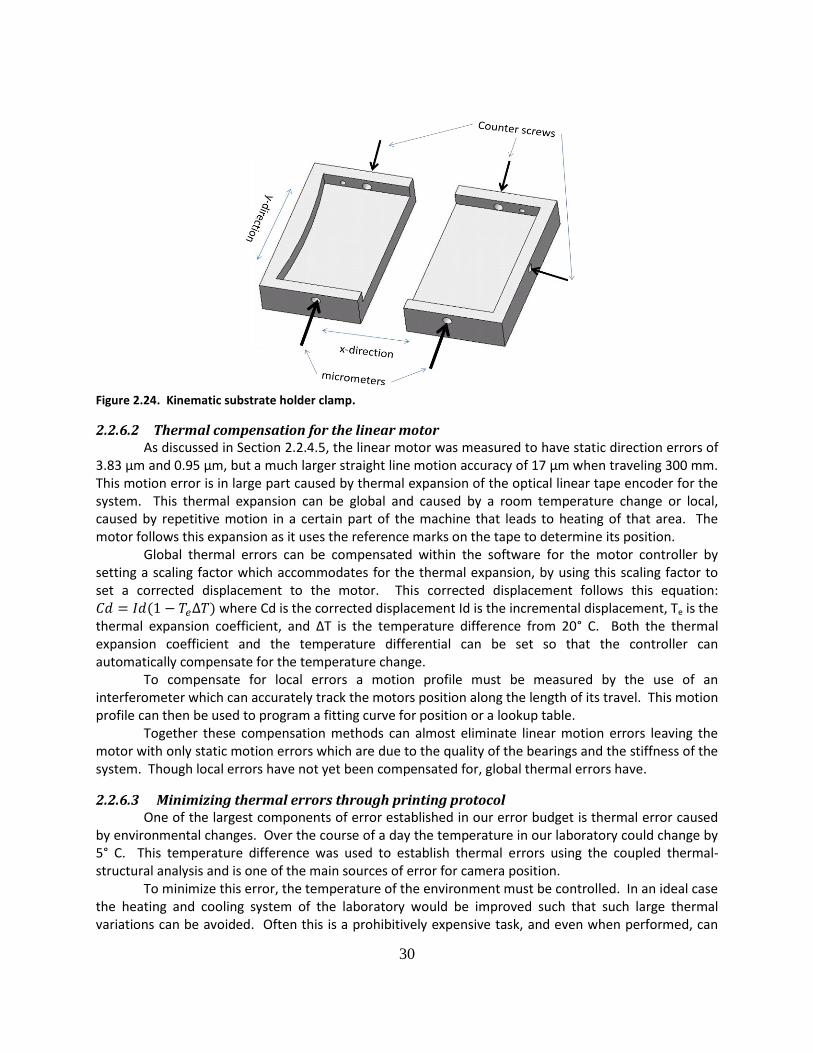
30
Figure 2.24. Kinematic substrate holder clamp.
2.2.6.2 Thermal compensation for the linear motor As discussed in Section 2.2.4.5, the linear motor was measured to have static direction errors of 3.83 μm and 0.95 μm, but a much larger straight line motion accuracy of 17 μm when traveling 300 mm. This motion error is in large part caused by thermal expansion of the optical linear tape encoder for the system. This thermal expansion can be global and caused by a room temperature change or local, caused by repetitive motion in a certain part of the machine that leads to heating of that area. The motor follows this expansion as it uses the reference marks on the tape to determine its position. Global thermal errors can be compensated within the software for the motor controller by setting a scaling factor which accommodates for the thermal expansion, by using this scaling factor to set a corrected displacement to the motor. This corrected displacement follows this equation:
where Cd is the corrected displacement Id is the incremental displacement, Te is the thermal expansion coefficient, and ∆T is the temperature difference from 20° C. Both the thermal expansion coefficient and the temperature differential can be set so that the controller can automatically compensate for the temperature change. To compensate for local errors a motion profile must be measured by the use of an interferometer which can accurately track the motors position along the length of its travel. This motion profile can then be used to program a fitting curve for position or a lookup table. Together these compensation methods can almost eliminate linear motion errors leaving the motor with only static motion errors which are due to the quality of the bearings and the stiffness of the system. Though local errors have not yet been compensated for, global thermal errors have.
2.2.6.3 Minimizing thermal errors through printing protocol One of the largest components of error established in our error budget is thermal error caused by environmental changes. Over the course of a day the temperature in our laboratory could change by 5° C. This temperature difference was used to establish thermal errors using the coupled thermal-structural analysis and is one of the main sources of error for camera position. To minimize this error, the temperature of the environment must be controlled. In an ideal case the heating and cooling system of the laboratory would be improved such that such large thermal variations can be avoided. Often this is a prohibitively expensive task, and even when performed, can
31
lead to mixed results, as temperature fluctuations can occur by opening and closing of doors or operation of equipment nearby. Advanced lithography and machining tools take a local approach to environmental control by using a temperature controlled environmental chamber which is built as part of the machine. These environmental chambers need only control the volume of space around the machine, and can thus more accurately control its temperature. In our case, temperature control is obtained through time management. Temperature changes in our laboratory are fairly slow, changing by no more than 0.5 °C per hour, and are usually caused by the natural temperature changes between night and day. The closer all printing processes can be carried in time, the smaller the temperature variations will be. As the duty cycle of our machine is very low, having to be operated only up four times for the completion of a TFT process, local heating not significant. Thus the printing protocol requires that motion calibration routines, and all alignment and print routines be carried out within a four hour period, where temperature variations are expected to be no more than 2° C, and are commonly 1° C or less. Another thermal error that can be compensated through printing protocol is that related to the gravure roll. As discussed, the gravure roll goes through a series of vigorous cleaning steps between prints. Some of these steps involve ultrasonic agitation which can easily cause temperature changes of 10°-20° C. To minimize the errors caused by the cleaning process, the roll must be placed in a large heat sink after ultrasonic agitation to equilibrate with room temperature. This heat sink is 5L of water which is kept continuously at room temperature, and a clean, solvent filled beaker which is set in this body prior to printing. Once cleaned, the roll is set in the solvent of the beaker, and the heat is dissipated before the roll is reused.
2.2.7 Error Analysis Summary This work shows the challenge of designing a printing tool that can achieve 5 μm layer-to-layer registration. Thermal and mechanical errors must be very carefully understood and controlled to avoid that their sum become larger than the maximum error tolerable. Without considering effects of the plastic substrate, we have found that the total system errors of the first embodiment of the gravure printer discussed are on the order of 50 μm in the print direction x, and 30 μm in the perpendicular direction y. Making use of kinematic clamp design has eliminated a large portion of the y-error. Using digital compensation has reduced many of the errors in the x-direction caused by temperature dependent motor motion. Finally ensuring that temperature changes in the environment are minimized during a multi-layered print has reduced a large component of the thermal errors. Together these changes should reduce the total printer error to 15 μm in the x-direction and 6 μm in the y-direction. We note that these models have not taken into account substrate distortion and we propose that this distortion accounts for a large portion of the discrepancy between the calculated error budget and the measured registration capability. We thus identify distortion control of flexible substrates a key area for further investigation.
2.3 Roll Patterning Not only are improvements in registration necessary to make gravure a viable process for electronics, but improvements in resolution are equally important. In graphic arts feature need only be small enough to fool the eye, but in electronics, feature scaling is a key component to better performance, lower power, and lower-cost The gravure roll serves as the master pattern for printing. Because of this, the resolution of the print is highly dependent on the quality of the patterns on the roll, and the surface and shape properties of the non-patterned areas. The minimum size of printed features is determined by the size of the patterns on the roll, the amount of ink they deposit, and the wetting properties of the ink. In graphic
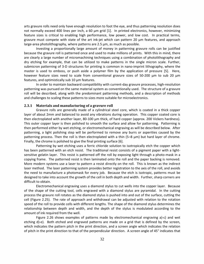
32
arts gravure rolls need only have enough resolution to foot the eye, and thus patterning resolution does not normally exceed 400 lines per inch, a 60 μm grid [1]. In printed electronics, however, minimizing feature sizes is critical to enabling high performance, low power, and low cost. In practical terms, gravure must compete with state of the art ink-jet which can pattern 20 μm features, and approach large-area photolithography, where patterns are 2.5 μm, as much as possible. Investing a proportionally large amount of money in patterning gravure rolls can be justified because the gravure roll is patterned once and used to make millions of prints. With this in mind, there are clearly a large number of micromachining techniques using a combination of photolithography and dry etching for example, that can be utilized to make patterns in the single micron scale. Further, submicron patterning of 3-D structures for printing is common in nano-imprint lithography, where the master is used to emboss, or push aside a polymer film by the application of pressure [5]. Here, however feature sizes need to scale from conventional gravure sizes of 50-200 μm to sub 20 μm features, and optimistically sub 10 μm features. In order to maintain backward compatibility with current-day gravure processes, high-resolution patterning was pursued on the same material system as conventionally used. The structure of a gravure roll will be described, along with the predominant patterning methods, and a description of methods and challenges to scaling these patterns to sizes more suitable for microelectronics.
2.3.1 Materials and manufacturing of a gravure roll Gravure rolls are generally made of a cylindrical steel core, which is coated in a thick copper layer of about 2mm and balanced to avoid any vibrations during operation. This copper coated core is then electroplated with another layer, 80-100 μm thick, of hard copper (approx. 200 Vickers hardness). This outer copper layer is then polished to smooth the surface and allow for patterning. Patterning is then performed either by wet etching, or electromechanical engraving as will be described below. After patterning, a light polishing step will be performed to remove any burrs or asperities caused by the patterning process. Then the roll is then electroplated with a thin (5–8 μm) but hard layer of chrome. Finally, the chrome is polished to give the final printing surface [6]. Patterning by wet etching uses a ferric chloride solution to isotropically etch the copper which has been patterned with an etch resist. The traditional resist consists of a pigment paper with a light-sensitive gelatin layer. This resist is patterned off the roll by exposing light through a photo-mask in a copying frame. The patterned resist is then laminated onto the roll and the paper backing is removed. More modern systems use a laser to pattern a resist directly on the roll. This is known as the indirect laser method. The laser patterning system provides better registration to the axis of the roll, and avoids the need to manufacture a photomask for every job. Because the etch is isotropic, patterns must be designed to take into account the growth of the cell in both depth and width. Further, sharp corners are difficult to obtain. Electromechanical engraving uses a diamond stylus to cut wells into the copper layer. Because of the shape of the cutting tool, cells engraved with a diamond stylus are pyramidal. In the cutting process the gravure roll rotates as the diamond stylus is pushed into and out of the surface, cutting the cell (Figure 2.25). The rate of approach and withdrawal can be adjusted with relation to the rotation speed of the roll to provide cells with different lengths. The shape of the diamond stylus determines the relationship between depth and width, and the depth of the stylus is modulated according to the amount of ink required from the well. Figure 2.26 shows examples of patterns made by electromechanical engraving a)-c) and wet etching d)-e). Both etched and engraved patterns are made on a grid that is defined by the screen, which indicates the pattern pitch in the print direction, and a screen angle which indicates the relation of pitch in the print direction to that of the perpendicular direction. A screen angle of 45° indicates that
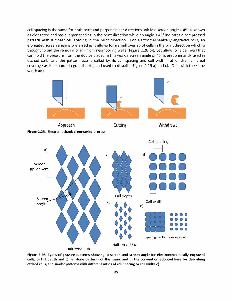
33
cell spacing is the same for both print and perpendicular directions, while a screen angle > 45° is known as elongated and has a larger spacing in the print direction while an angle < 45° indicates a compressed pattern with a closer cell spacing in the print direction. For electromechanically engraved rolls, an elongated screen angle is preferred as it allows for a small overlap of cells in the print direction which is thought to aid the removal of ink from neighboring wells (Figure 2.26 b)), yet allow for a cell wall that can hold the pressure from the doctor blade. In this work a screen angle of 45° is predominantly used in etched cells, and the pattern size is called by its cell spacing and cell width, rather than an areal coverage as is common in graphic arts, and used to describe Figure 2.26 a) and c). Cells with the same width and
Figure 2.25. Electromechanical engraving process.
Figure 2.26. Types of gravure patterns showing a) screen and screen angle for electromechanically engraved cells, b) full depth and c) half-tone patterns of the same, and d) the convention adopted here for describing etched cells, and similar patterns with different ratios of cell spacing to cell width e).
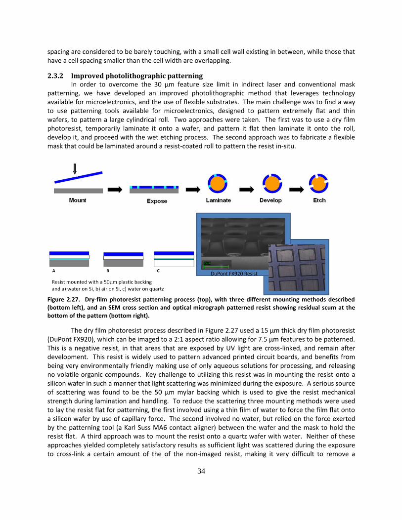
34
spacing are considered to be barely touching, with a small cell wall existing in between, while those that have a cell spacing smaller than the cell width are overlapping.
2.3.2 Improved photolithographic patterning In order to overcome the 30 μm feature size limit in indirect laser and conventional mask patterning, we have developed an improved photolithographic method that leverages technology available for microelectronics, and the use of flexible substrates. The main challenge was to find a way to use patterning tools available for microelectronics, designed to pattern extremely flat and thin wafers, to pattern a large cylindrical roll. Two approaches were taken. The first was to use a dry film photoresist, temporarily laminate it onto a wafer, and pattern it flat then laminate it onto the roll, develop it, and proceed with the wet etching process. The second approach was to fabricate a flexible mask that could be laminated around a resist-coated roll to pattern the resist in-situ.
Figure 2.27. Dry-film photoresist patterning process (top), with three different mounting methods described (bottom left), and an SEM cross section and optical micrograph patterned resist showing residual scum at the bottom of the pattern (bottom right).
The dry film photoresist process described in Figure 2.27 used a 15 μm thick dry film photoresist (DuPont FX920), which can be imaged to a 2:1 aspect ratio allowing for 7.5 μm features to be patterned. This is a negative resist, in that areas that are exposed by UV light are cross-linked, and remain after development. This resist is widely used to pattern advanced printed circuit boards, and benefits from being very environmentally friendly making use of only aqueous solutions for processing, and releasing no volatile organic compounds. Key challenge to utilizing this resist was in mounting the resist onto a silicon wafer in such a manner that light scattering was minimized during the exposure. A serious source of scattering was found to be the 50 μm mylar backing which is used to give the resist mechanical strength during lamination and handling. To reduce the scattering three mounting methods were used to lay the resist flat for patterning, the first involved using a thin film of water to force the film flat onto a silicon wafer by use of capillary force. The second involved no water, but relied on the force exerted by the patterning tool (a Karl Suss MA6 contact aligner) between the wafer and the mask to hold the resist flat. A third approach was to mount the resist onto a quartz wafer with water. Neither of these approaches yielded completely satisfactory results as sufficient light was scattered during the exposure to cross-link a certain amount of the of the non-imaged resist, making it very difficult to remove a
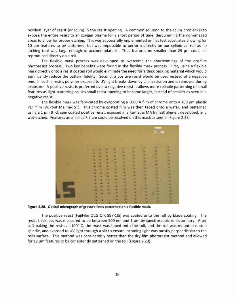
35
residual layer of resist (or scum) in the resist opening. A common solution to the scum problem is to expose the entire resist to an oxygen plasma for a short period of time, descumming the non-imaged areas to allow for proper etching. This was successfully implemented on flat test substrates allowing for 10 μm features to be patterned, but was impossible to perform directly on our cylindrical roll as no etching tool was large enough to accommodate it. Thus features no smaller than 25 μm could be reproduced directly on a roll. The flexible mask process was developed to overcome the shortcomings of the dry-film photoresist process. Two key benefits were found in the flexible mask process. First, using a flexible mask directly onto a resist coated roll would eliminate the need for a thick backing material which would significantly reduce the pattern fidelity. Second, a positive resist would be used instead of a negative one. In such a resist, polymer exposed to UV light breaks down by chain scission and is removed during exposure. A positive resist is preferred over a negative resist it allows more reliable patterning of small features as light scattering causes small resist opening to become larger, instead of smaller as seen in a negative resist. The flexible mask was fabricated by evaporating a 1000 Å film of chrome onto a 100 μm plastic PET film (DuPont Melinex ST). This chrome coated film was then taped onto a wafer, and patterned using a 1 μm thick spin coated positive resist, exposed in a Karl Suss MA 6 mask aligner, developed, and wet-etched. Features as small as 7.5 μm could be resolved on this mask as seen in Figure 2.28.
Figure 2.28. Optical micrograph of gravure lines patterned on a flexible mask.
The positive resist (FujiFilm OCG OiR 897-10i) was coated onto the roll by blade coating. The resist thickness was measured to be between 500 nm and 1 μm by spectroscopic reflectometry. After soft baking the resist at 100° C, the mask was taped onto the roll, and the roll was mounted onto a spindle, and exposed to UV light through a slit to ensure incoming light was mostly perpendicular to the rolls surface. This method was considerably better than the dry-film photoresist method and allowed for 12 μm features to be consistently patterned on the roll (Figure 2.29).
30 μm
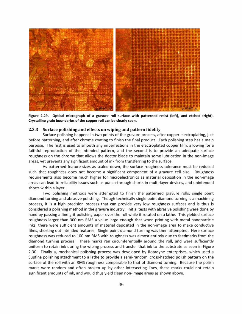
36
Figure 2.29. Optical micrograph of a gravure roll surface with patterned resist (left), and etched (right). Crystalline grain boundaries of the copper roll can be clearly seen.
2.3.3 Surface polishing and effects on wiping and pattern fidelity Surface polishing happens in two points of the gravure process, after copper electroplating, just before patterning, and after chrome coating to finish the final product. Each polishing step has a main purpose. The first is used to smooth any imperfections in the electroplated copper film, allowing for a faithful reproduction of the intended pattern, and the second is to provide an adequate surface roughness on the chrome that allows the doctor blade to maintain some lubrication in the non-image areas, yet prevents any significant amount of ink from transferring to the surface. As patterned feature sizes as scaled down, the surface roughness tolerance must be reduced such that roughness does not become a significant component of a gravure cell size. Roughness requirements also become much higher for microelectronics as material deposition in the non-image areas can lead to reliability issues such as punch-through shorts in multi-layer devices, and unintended shorts within a layer. Two polishing methods were attempted to finish the patterned gravure rolls: single point diamond turning and abrasive polishing. Though technically single point diamond turning is a machining process, it is a high precision process that can provide very low roughness surfaces and is thus is considered a polishing method in the gravure industry. Initial tests with abrasive polishing were done by hand by passing a fine grit polishing paper over the roll while it rotated on a lathe. This yielded surface roughness larger than 300 nm RMS a value large enough that when printing with metal nanoparticle inks, there were sufficient amounts of material deposited in the non-image area to make conductive films, shorting out intended features. Single point diamond turning was then attempted. Here surface roughness was reduced to 100 nm RMS with roughness was almost entirely due to feedmarks from the diamond turning process. These marks ran circumferentially around the roll, and were sufficiently uniform to retain ink during the wiping process and transfer that ink to the substrate as seen in Figure 2.30. Finally a, mechanical polishing process was developed by Rotadyne enterprises, which used a Supfina polishing attachment to a lathe to provide a semi-random, cross-hatched polish pattern on the surface of the roll with an RMS roughness comparable to that of diamond turning. Because the polish marks were random and often broken up by other intersecting lines, these marks could not retain significant amounts of ink, and would thus yield clean non-image areas as shown above.
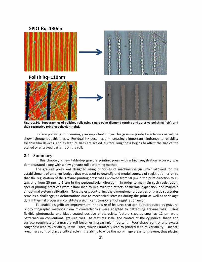
37
Figure 2.30. Topographies of polished rolls using single point diamond turning and abrasive polishing (left), and their respective printing behavior (right).
Surface polishing is increasingly an important subject for gravure printed electronics as will be shown throughout this thesis. Residual ink becomes an increasingly important hindrance to reliability for thin film devices, and as feature sizes are scaled, surface roughness begins to affect the size of the etched or engraved patterns on the roll.
2.4 Summary In this chapter, a new table-top gravure printing press with a high registration accuracy was demonstrated along with a new gravure roll patterning method. The gravure press was designed using principles of machine design which allowed for the establishment of an error budget that was used to quantify and model sources of registration error so that the registration of the gravure printing press was improved from 50 μm in the print direction to 15 μm, and from 20 μm to 6 μm in the perpendicular direction. In order to maintain such registration, special printing practices were established to minimize the effects of thermal expansion, and maintain an optimal system calibration. Nonetheless, controlling the dimensional properties of plastic substrates remains a challenge, as deformations due to mechanical stresses during the print as well as shrinkage during thermal processing constitute a significant component of registration error. To enable a significant improvement in the size of features that can be reproduced by gravure, photolithographic methods from microelectronics were adapted to patterning gravure rolls. Using flexible photomasks and blade-coated positive photoresists, feature sizes as small as 12 μm were patterned on conventional gravure rolls. As features scale, the control of the cylindrical shape and surface roughness of a gravure roll becomes increasingly important. Poor shape control and excess roughness lead to variability in well sizes, which ultimately lead to printed feature variability. Further, roughness control plays a critical role in the ability to wipe the non-image areas for gravure, thus placing

38
a high importance on roll finishing processes. A semi-random, cross-hatch polish pattern was established to be the best choice for minimizing unwanted ink transfer. Together, these advances provide a great laboratory tool that will allow gravure to be used to print feature sizes well below those used in graphics arts and suitable for printed electronics.
2.5 Works Cited [1] Kipphan, Helmut., Handbook of Print Media: Technologies and Production Methods. Berlin : Springer-Verlag, 2001. p. 1207. isbn 3-540-67326-1. [2] Murata, Kazuhiro., "Super-fine ink-jet printing for nanotechnology." s.l. : Proceedings of the Internation Conference on MEMS, NANO, and Smart Systems (ICMENS'03), 20-23 July 2003. pp. 346-349. [3] Park, Jang-Ung, et al., "High-resolution electrohydrodynamic jet printing." s.l. : Nature Materials, 2007. pp. 782-790. doi:10.1038/nmat1974. [4] Dornfeld, David and Lee, Dae-Eun., Precision Manufacturing. s.l. : Springer, 2008. p. 775. ISBN: 978-0-387-32467-8. [5] Chou, Stephe Y., Krauss, Petter and Renstrom, Preston J., "Imprint Lithography with 25-Nanometer Resolution." s.l. : Science, 1996, Vol. 272, pp. 85 - 87. DOI: 10.1126/science.272.5258.85. [6] Rutherford, Brett ed., Gravure Process and Technology. Rochester : Gravure Association of America, 1991. ISBN 1-880290-00-6.
39
3 Printed Metal Lines Conductive traces are at the heart of all electronics, communications, and power systems since they provide low resistance interconnection and current flow paths. In electronics, conductive traces serve a variety of purposes from interconnection between integrated circuits at the system level on printed circuit boards, to interconnects between transistors and other devices at the back-end of the integrated circuit process, to contacts to and intrinsic components of the semiconductor devices themselves. Because printed electronics hopes to bring the production of system level circuitry, packaging, back-end and front-end integrated circuitry together, it is important to identify and improve the critical characteristics of metal traces for each one of these applications. This chapter will discuss these issues and explain how this has led to the development of a variety of printing processes using different materials and different scaling criteria to achieve well behaved metallic lines.
3.1 Performance criteria for metallic lines In flexible electronics the function of the printed circuit board, the back-end interconnection and the front-end contacts of an integrated circuit will be integrated onto the same substrate and hopefully deposited with minimal number of steps. However, to make sure each one of these three different types of lines is optimized the characteristics required for each must first be identified.
3.1.1 Printed Circuit Boards Printed circuit boards are ubiquitous to all electronic devices as they both as the substrate and the framework on which integrated circuits are connected to make a usable device. Printed circuit boards are most commonly composed of multiple layers of dielectric each with metallic traces and vias to interconnect traces between various layers of the printed circuit board. The dielectric for PCB’s is most commonly some glass fiber impregnated with an epoxy binder but can also be composed of a cotton fiber in epoxy resin. The metal used is almost exclusively copper, because of its good conductivity and ease of processing but could be any metal including aluminum (lower cost) or silver (higher conductivity), as long as the overall process and performance requirements are met. In the case of PCB’s the metal layers provide power, communication, and mechanical support for components and ICs which are bonded to them. Therefore it is critical that these metal traces provide low resistance, mechanical robustness, solderability, low cross-talk, and minimum electromagnetic interference (EMI). Because of packaging limits for IC’s and the size of discrete components, feature size is generally a secondary concern for metal traces in PCBs. Nonetheless the need for improved circuit density and tighter packaging to satisfy a growing array of complex mobile devices has begun to push feature size requirements for PCBs into the 50 μm, and possibly further into the 20 μm range for what are called high density interconnects (HDI) [1].
The products that drive high density interconnect development demand not only a very high density circuit board with ever decreasing pitches, they are also very cost sensitive, and thus pressure PCB manufacturers to control costs carefully. One technology that has been developed to meet these demands is sequential build up circuits, in which multi-layer PCBs are created not by laminating sheets of dielectric but by building up the various metal layers through the deposition of thick polymer layers which can be easily patterned to form vias, therefore eliminating costly drilling processes used in conventional PCBs [1].
Because of the promise for low cost and small feature size, printed electronics has a large potential to bring significant value to this field.
40
3.1.2 Flexible Circuit Boards The development of ever more complex mobile devices has also driven a large amount of
development in flexible circuit boards. Originally used as mere interconnects between conventional PCBs to enable tighter packing and 3-D circuits, flexible circuit boards have advanced to multi-layer structures capable of holding surface mount and through hole devices, and the complexity of these structures has been catching up with those of PCBs to achieve high density interconnects and even ultra-high density interconnects with via hole sizes below 50 μm and fine lines with 25 μm pitch to meet the high I/O counts and tight packing densities required in devices such as digital cameras and mobile phones [1].
While the electrical and some of the mechanical requirements of metal traces for flexible circuit boards are similar to those of rigid PCBs, the added requirement of flexibility, sometimes with a requirement of very high dynamic flexing lifetimes with high duty cycle (such as used in hard disk drives) requires special consideration.
The fabrication process for flexible circuit boards follows a very similar pattern to that of rigid circuit boards, commonly using copper as the conductor, and starting with either laminated copper films or electroplated films over a sputtered seed layer, then continuing through a mask and etch process for patterning. However, the additional need to carefully control dimensional stability during processing, the limited thermal budged allowed by the polymeric substrates, issues of moisture absorption, and a more complex process of using a coverlay instead of a solder mask to protect traces during flexing can easily make flexible circuit boards cost prohibitive. Here again, high resolution all-additive printed metallic traces in combination with printed dielectric interlayers can provide significant cost as well as performance advantage.
For some applications such as antennas for RFID, circuit boards for keyboards and segmented displays, cost plays the most critical factor, and thus fully printed processes for these simple circuits have already become available lending credence to the viability and benefit of printing.
3.1.3 Back-end interconnects “Back-end technology refers to the interconnect layers, contacts, vias and dielectric layers that wire the active devices into a specific circuit configuration.” [2] Despite the fact that the use of the term “back-end” is used almost exclusively for crystalline large-scale integrated circuits, the above quote makes it clearly evident that this category of metallization is critical to any type of integrated circuit. Though a proper back-end process may not exist in the same form for printed electronics as it does for conventional electronics, materials and processes must be developed to enable the functionality of interconnects, vias, contacts, and dielectric layers needed to make functional printed circuits feasible. Further, to maximize the speed of manufacture, and lower overall cost, it is important minimize the number of process steps involved in completing the back-end process. Printed metals used in the back end process must thus be able to make clean ohmic contacts to devices, and interconnect these devices using a design that combines both minimum pitch lines to reduce overall packing density, and minimum resistivity to reduce the RC delay [3]. The first layer of metallization will often be only sufficient to connect devices to other nearby devices via their gates and source/drain terminals, making simple logic devices such as buffers, inverters, and memory. The resistivity is less important than the minimum pitch at this point since the distances covered are generally small. To complete more complex logic functions, the core logic elements must be interconnected, and this usually means adding another layer of interconnects. Interlayer dielectrics and metal vias must then be placed to connect the two layers. Printed metals in this case must be able to properly fill via holes,

41
make ohmic contact to the lower metal layer, and not damage the interlayer dielectric. Here these metal interconnects must provide a lower resistance as they are longer, providing global interconnections. Since there may be multiple interconnect layers, the interconnects must also withstand the subsequent process steps, not being damaged by the solvents or thermal cycles involved. The uniformity of the printed metal layers and choice of metal is also very important. Uniformity must be maximized to prevent high-resistance regions which may lead to local heating, and accelerated electromigration. Metals with a low susceptibility to electromigration should be chosen to minimize the effects of film non-uniformity, and also avoid accidental shorts between traces that may be DC biased against each other for long periods of time. In conventional electronics the performance of interconnect structures has become increasingly important to overall chip performance as complexity has increased and devices have scaled down in size. Most notably this has lead to an increase in the RC time delay of signals propagating in the interconnects, slowing the overall speed of the circuit. In printed electronics, device performance is considerably lower and pitches considerably larger. However, the distances covered in many applications are incredibly large, and thus a similar importance must be placed on the back-end process.
3.1.4 Contacts to devices On the front end of the process, metals serve as either ohmic or rectifying contacts to
semiconductors as well as contacts to insulators. The role these metals play is as critical as any in the performance of the device, as they can be a limiting if not determining factor of device yield and performance.
The choice of metal becomes important in the front end as the electronic alignment of this metal to either a semiconductor or dielectric becomes important. When contacting a semiconductor with a metal either an ohmic or rectifying junction can be created depending on how the metal work-function lines up with the Fermi-level of the semiconductor, or the nature of interface states at the junction as described in Chapter 5. Because most semiconductor devices are composed of multiple layers of thin films, not only do the electronic properties of the metals used matter, but also the physical quality of the deposited films. Because these metals may compose part of a stack no thicker than a few hundred nanometers, it is critical that they can be deposited in such a manner that they remain uniformly thin, with no pinholes, cracks, or protrusions, and that they can withstand the stresses of further processing or use. The roughness created by any of the aforementioned defects can have deleterious effects on the performance of the device and will be discussed throughout the chapter.
3.2 Types of metallic inks As mentioned in Chapter 1, ability to deposit functional materials via solution has been the key enabler to printed electronics. For metals, various approaches have been used to formulate inks that provide metallic films. They key component of these inks categorize their type, listed here: conducting polymers, metal flakes, metal nanoparticles, and metal-organic/metal-salt precursors. The most obvious approach to obtaining a conducting film from solution is to use a powder of an elemental metal. This is perhaps why metal flake inks are the most widely used and lowest cost. Ink formulation can be as simple as taking pieces of a metal and grinding them down to micrometer sized flakes using a ball mill, then dispersing the resulting flakes in a solvent/polymer mixture to provide an ink of the required viscosity. The ink provides conductive films thanks to physical contact between metal flakes which provide a percolation network for electrons to travel through. The simplicity of the manufacturing process makes the ink cost only a fraction more than the raw materials cost. Because the
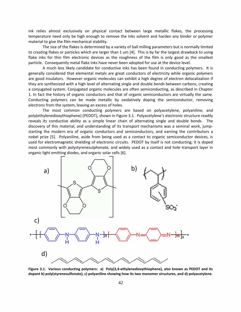
42
ink relies almost exclusively on physical contact between large metallic flakes, the processing temperature need only be high enough to remove the inks solvent and harden any binder or polymer material to give the film mechanical stability. The size of the flakes is determined by a variety of ball milling parameters but is normally limited to creating flakes or particles which are larger than 1 um [4]. This is by far the largest drawback to using flake inks for thin film electronic devices as the roughness of the film is only good as the smallest particle. Consequently metal flake inks have never been adopted for use at the device level. A much less likely candidate for conductive inks has been found in conducting polymers. It is generally considered that elemental metals are great conductors of electricity while organic polymers are good insulators. However organic molecules can exhibit a high degree of electron delocalization if they are synthesized with a high level of alternating single and double bonds between carbons, creating a conjugated system. Conjugated organic molecules are often semiconducting, as described in Chapter 1. In fact the history of organic conductors and that of organic semiconductors are virtually the same. Conducting polymers can be made metallic by oxidatively doping the semiconductor, removing electrons from the system, leaving an excess of holes. The most common conducting polymers are based on polyacetylene, polyaniline, and poly(ethylenedioxythiophene) (PEDOT), shown in Figure 3.1. Polyacetylene’s electronic structure readily reveals its conductive ability as a simple linear chain of alternating single and double bonds. The discovery of this material, and understanding of its transport mechanisms was a seminal work, jump-starting the modern era of organic conductors and semiconductors, and earning the contributors a nobel prize [5]. Polyaniline, aside from being used as a contact to organic semiconductor devices, is used for electromagnetic shielding of electronic circuits. PEDOT by itself is not conducting; it is doped most commonly with polystyrenesulphonate, and widely used as a contact and hole transport layer in organic light emitting diodes, and organic solar cells [6].
Figure 3.1. Various conducting polymers: a) Poly(3,4-ethylenedioxythiophene), also known as PEDOT and its dopant b) poly(styrenesulfonate), c) polyaniline showing how its two monomer structures, and d) polyacetylene.
43
In general polymers are easy to dissolve and inks with good rheological behavior can be made with them. Conducting polymers are more difficult to formulate as an ink because the materials are often salt-like, making it difficult to dissolve them into organic solvents. Further their conductivity is highly dependent on their oxidative state, which is susceptible to degradation by oxygen and atmospheric moisture. Finally their synthesis can be complex compared to metals and thus fail to bring a considerable cost advantage, yet provide orders of magnitude higher resistivity. However, their electronic compatibility with organic semiconductors, their low temperature processing, and relatively smooth films have allowed conducting polymers to obtain the widest adoption in thin-film devices of any printable conductor, particularly in organic light emitting diodes. Another candidate conductor ink family is based on metallic nanoparticles. Nanoparticle based inks provide highly conductive films at low processing temperatures. They take advantage of the fact that the melting temperature of the metals they use is significantly depressed as the materials are constrained to nanometer-scale crystals [7][8][9]. The resulting films are composed of a large percentage of elemental metals with a relatively low quantity of organic compounds. Our group was one of the first to report on the use of the melting temperature depression of nanoparticles to formulate a printable gold ink which can be easily converted into an electronic interconnect or contact with up to 80% of bulk metal performance [10] allowing the fabrication of all ink-jet printed, high-performance transistors [11]. Since then a wide number of companies have developed nanoparticle inks for printed electronics using a variety of metals including gold, silver, nickel, platinum, palladium, and copper. Aside from polymeric conductive inks, and flake inks, they are the most widely studied and produced. Silver has become the most widely adopted metal for printable inks. Silver is considerably less expensive that gold, despite it being the best understood nanoparticle system, and does not suffer exhibit a serious of conductivity due to oxidation as does copper and aluminum which form insulating oxides (silver oxide is conductive). Further, a wide variety of synthetic approaches to silver nanoparticles have been developed including the reduction of silver ions with or without capping agents, photoreduction in reverse micelles, and thermal decomposition of organic solvents [12]. The diversity of synthetic pathways has facilitated the formulation of printable inks with silver nanoparticles. Silver nanoparticle inks can be made with a wide range of mass loading, varying from < 10% up to 80% silver by mass, and a wide range of viscosities, ranging from < 10 cP inks for ink-jet printing to 10,000 cP pastes for screen printing and thick film applications. Most of these formulations require sintering temperatures above 200° C to achieve full conversion of the inks, yet achieve conductive films at temperatures as low as 150° C with moderately higher resistivities. In general nanoparticle inks are excellent candidates for printed electronics because of the high performance films they produce, the wide variety of available materials (and therefore work-functions), and the plastic compatible temperatures at which they can be processed. Yet issues of colloidal stability, printability, film roughness, purity of their final films, and susceptibility to electromigration have not been fully resolved, and are under investigation in order to allow the broad adoption of these materials for semiconductor device use. A final class of conductor inks is based on metal-containing precursors. Metal-organic complexes, organometallics, and metal salts have been used as photosensitive materials for photographic film, precursors for deposition of III-V materials with metallo-organic chemical vapor deposition (MOCVD), sol-gel processing, and as facile methods to deposit anti-static, and reflective films. Organometallic compounds are chemical compounds containing bonds between carbon and a metal and are broadly studied in the field of organometallic chemistry.
44
Their uses as precursors to metallic traces for microelectronics begin in plating processes for printed circuit boards. Direct patterning of such materials has existed for some time. In 1987 a demonstration was made using ink-jet printing to pattern silver metalorganic decomposition (MOD) ink, as well as a high-k dielectric such as lead titanate for hybrid microelectronic ciruits [13]. Matsushita Electric Industrial Co. filed patents in 1991 on the use of organometallics to deposit and intaglio print transparent conducting oxides, as well as metals of various types[14][15]. In 1993 Sceisi et. al. reported using a spin-on gold metallorganic and laser direct writing to pattern interconnects on silicon dioxide [16]. By then others had demonstrated the use of organometallics for mask repair, microelectronic interconnects, and contacts to optoelectronic devices. More recently, better formulations of organometallic and metal-salt complexes have become available that exhibit better stability, and lower processing temperature than previously reported materials. One such example was recently presented by Wu [17]. In this work, a solution of a silver salt such as silver acetate, an ethanolamine, and a long chain carboxylic acid is dissolved in an alcohol solvent. The silver salt in this solution is known to self-reduce to silver at high temperatures, or readily by exposure to a strong reducing agent such as NaBH4. The addition of weak reducing agents like the ethanolamine and carboxylic acid allows for stability of the ink, yet low processing temperature. The chain length of the carboxylic acid is adjusted to control the reaction rate and rate of evaporation of the acid, improving the film uniformity. With such an approach inks can be formulated with up to 20% mass loading of silver. Further the lines they provide are thin, smooth and uniform in thickness with a conductivity of 105 S/cm. Organometallic inks tend to be lower cost than their nanoparticle counterparts. In fact sometimes they are the same precursors used to synthesize nanoparticles [18]. They are also easy to prepare into an ink which has much better stability and rheological properties than a nanoparticle or flake-based ink, because they are true solvent/solute systems. However they provide low viscosity inks, and because of their low mass loading can lead to films of poor mechanical quality as described below. Finally, like nanoparticle inks, their final films retain residual ligands, stabilizers, and reactants in them which can leach into or react with the materials they come into contact with. The goal in printing these inks is to print low-resistance interconnects, and contacts to thin film devices using gravure. This work focuses mainly on the use of metal nanoparticle and organometallic inks because they provide the best combination of smooth thin films and low resistance. Flake inks are not further discussed because the minimum pitch, film thickness, and roughness they can provide is larger than intended for the scope of this work. Conductive polymers, are not further discussed because they are well studied for these applications, and because they provide films of relatively high resistivity, which hampers the speed of the circuits they would be used to create. However, it is worthy to note that there is still potential to use these polymers as contact layers to semiconductors, where specific band alignments may be required, and their sparse use would not dramatically increase resistance in a circuit. Before describing the printing of these materials, however, a discussion of roughness is in order, as it turns out that the roughness of these films is a critical component to their successful adoption in microelectronics, more specifically, in thin film devices.
3.3 Roughness of printed metal films and lines When discussing roughness it is important to understand what the quoted measurements mean. Often, people will quote a specific value for RMS roughness or average roughness. What is not commonly understood is exactly what that value says about the surface, and whether or not this was exactly the correct value to quote. Thus roughness values can vary dramatically from source to source.

45
Because the roughness of films play a critical role in the performance and yield of all thin film devices, this section will deal with the fundamentals of roughness, the roughness properties of various ink based metal films, and the roughness of printed lines made with the aforementioned inks.
3.3.1 Roughness Roughness can be understood in many ways. It is the high-frequency short-wavelength component of the topography of a surface; the component of the surface which deviates from its ideal shape; that which deviates from a smooth surface. It can be caused by a wide variety of phenomena, depending on how the surface was made. Often it is an unintended feature. Sometimes it is a necessary and deliberate surface property. Regardless of the shape, its exact definition varies slightly depending on the needs and expectations of the person who studies it. Yet as a measurement, roughness is defined by a series of parameters that are obtained through a strict set of equations. So how can measurements of roughness vary so much? Looking at some of the parameters that describe roughness and how they are obtained, should elucidate the problem.
Figure 3.2. Simulated surface cross-section composed of nominal surface, waviness, and roughness components.
The most common roughness parameters quoted are average roughness (Ra), and RMS roughness (Rq). Average roughness calculates the arithmetic average of the vertical deviations of a surface from its ideal shape. Figure 3.2 shall be used to clarify the discussion. The left graph in the Figure 3.2 is a simulated shape profile, which could easily be a measured surface topography of a curved surface, such as a printed line, this shall be called the measured surface. The average roughness can be extracted from this figure by subtracting the measured surface, from the expected surface, labeled nominal surface on the figure, and taking the arithmetic mean of the resulting difference using the following equation:
(1) or
(2) when using discrete data.
The computation for average roughness seems clear enough. However a major assumption was made during the calculation. It was assumed that was defined by the nominal shape in Figure 3.2.
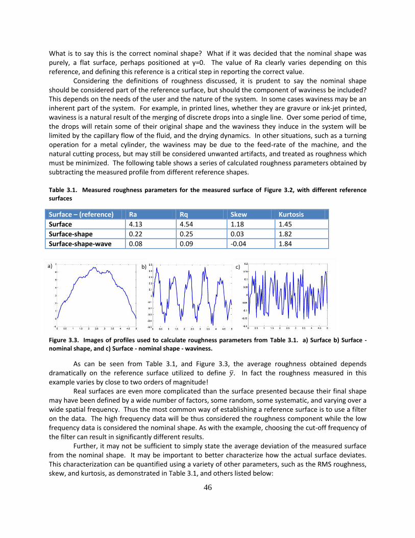
46
What is to say this is the correct nominal shape? What if it was decided that the nominal shape was purely, a flat surface, perhaps positioned at y=0. The value of Ra clearly varies depending on this reference, and defining this reference is a critical step in reporting the correct value. Considering the definitions of roughness discussed, it is prudent to say the nominal shape should be considered part of the reference surface, but should the component of waviness be included? This depends on the needs of the user and the nature of the system. In some cases waviness may be an inherent part of the system. For example, in printed lines, whether they are gravure or ink-jet printed, waviness is a natural result of the merging of discrete drops into a single line. Over some period of time, the drops will retain some of their original shape and the waviness they induce in the system will be limited by the capillary flow of the fluid, and the drying dynamics. In other situations, such as a turning operation for a metal cylinder, the waviness may be due to the feed-rate of the machine, and the natural cutting process, but may still be considered unwanted artifacts, and treated as roughness which must be minimized. The following table shows a series of calculated roughness parameters obtained by subtracting the measured profile from different reference shapes. Table 3.1. Measured roughness parameters for the measured surface of Figure 3.2, with different reference surfaces
Surface – (reference) Ra Rq Skew Kurtosis
Surface 4.13 4.54 1.18 1.45
Surface-shape 0.22 0.25 0.03 1.82
Surface-shape-wave 0.08 0.09 -0.04 1.84
Figure 3.3. Images of profiles used to calculate roughness parameters from Table 3.1. a) Surface b) Surface - nominal shape, and c) Surface - nominal shape - waviness.
As can be seen from Table 3.1, and Figure 3.3, the average roughness obtained depends dramatically on the reference surface utilized to define . In fact the roughness measured in this example varies by close to two orders of magnitude! Real surfaces are even more complicated than the surface presented because their final shape may have been defined by a wide number of factors, some random, some systematic, and varying over a wide spatial frequency. Thus the most common way of establishing a reference surface is to use a filter on the data. The high frequency data will be thus considered the roughness component while the low frequency data is considered the nominal shape. As with the example, choosing the cut-off frequency of the filter can result in significantly different results. Further, it may not be sufficient to simply state the average deviation of the measured surface from the nominal shape. It may be important to better characterize how the actual surface deviates. This characterization can be quantified using a variety of other parameters, such as the RMS roughness, skew, and kurtosis, as demonstrated in Table 3.1, and others listed below:

47
Parameter Description Formula
Ra Average roughness
Rq Root mean square (RMS) roughness (3)
Rv Maximum valley depth (4)
Rp Maximum peak height (5)
Rsk Skewness (6)
Rku Kurtosis (7)
Rz Average distance between highest peaks and lowest valleys
(8)
Depending on the application, only certain parameters may be of interest and may be needed to track the roughness of a surface. On the other hand, for certain applications some parameters may not be significant to the application and their use may in fact be misleading. Understanding what characteristic of a surface a roughness parameter estimates is of critical importance.
Figure 3.4. Profiles with different values of skew and the corresponding amplitude probability density functions.
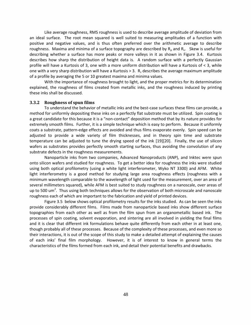
48
Like average roughness, RMS roughness is used to describe average amplitude of deviation from an ideal surface. The root mean squared is well suited to measuring amplitudes of a function with positive and negative values, and is thus often preferred over the arithmetic average to describe roughness. Maxima and minima of a surface topography are described by Rp and Rv. Skew is useful for describing whether a surface has more peaks or more valleys in it as shown in Figure 3.4. Kurtosis describes how sharp the distribution of height data is. A random surface with a perfectly Gaussian profile will have a Kurtosis of 3, one with a more uniform distribution will have a Kurtosis of < 3, while one with a very sharp distribution will have a Kurtosis > 3. Rz describes the average maximum amplitude of a profile by averaging the 5 or 10 greatest maxima and minima values. With the importance of roughness brought to light, and the proper metrics for its determination explained, the roughness of films created from metallic inks, and the roughness induced by printing these inks shall be discussed.
3.3.2 Roughness of spun films To understand the behavior of metallic inks and the best-case surfaces these films can provide, a method for uniformly depositing these inks on a perfectly flat substrate must be utilized. Spin coating is a great candidate for this because it is a “non-contact” deposition method that by its nature provides for extremely smooth films. Further, it is a simple technique which is easy to perform. Because it uniformly coats a substrate, pattern-edge effects are avoided and thus films evaporate evenly. Spin speed can be adjusted to provide a wide variety of film thicknesses, and in theory spin time and substrate temperature can be adjusted to tune the drying speed of the ink [19][20]. Finally, the use of silicon wafers as substrates provides perfectly smooth starting surfaces, thus avoiding the convolution of any substrate defects in the roughness measurements. Nanoparticle inks from two companies, Advanced Nanoproducts (ANP), and Inktec were spun onto silicon wafers and studied for roughness. To get a better idea for roughness the inks were studied using both optical profilometry (using a white light interferometer, Wyko NT 3300) and AFM. White light interferometry is a good method for studying large area roughness effects (roughness with a minimum wavelength comparable to the wavelength of light used for the measurement, over an area of several millimeters squared), while AFM is best suited to study roughness on a nanoscale, over areas of up to 500 um2. Thus using both techniques allows for the observation of both microscale and nanoscale roughness each of which are important to the fabrication and yield of printed devices. Figure 3.5 below shows optical profilometry results for the inks studied. As can be seen the inks provide considerably different films. Films made from nanoparticle based inks show different surface topographies from each other as well as from the film spun from an organometallic based ink. The processes of spin coating, solvent evaporation, and sintering are all involved in yielding the final films and it is clear that different ink formulations behave quite differently from each other in at least one, though probably all of these processes. Because of the complexity of these processes, and even more so their interactions, it is out of the scope of this study to make a detailed attempt of explaining the causes of each inks’ final film morphology. However, it is of interest to know in general terms the characteristics of the films formed from each ink, and detail their potential benefits and drawbacks.
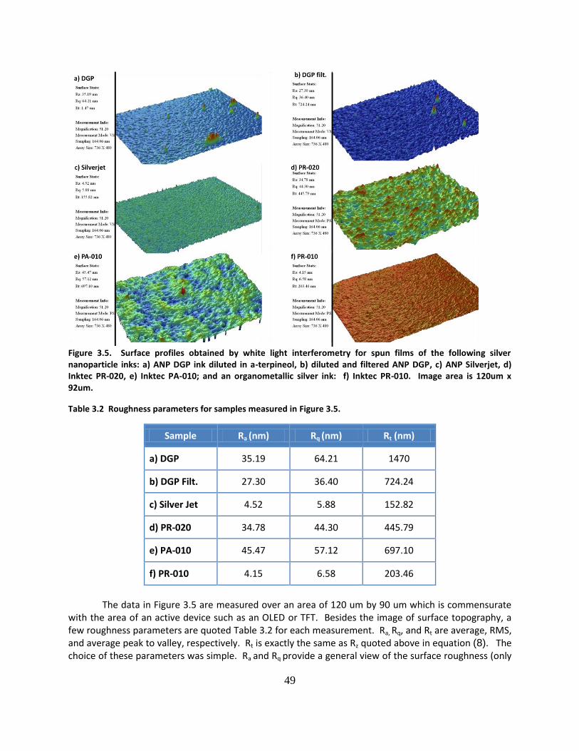
49
Figure 3.5. Surface profiles obtained by white light interferometry for spun films of the following silver nanoparticle inks: a) ANP DGP ink diluted in a-terpineol, b) diluted and filtered ANP DGP, c) ANP Silverjet, d) Inktec PR-020, e) Inktec PA-010; and an organometallic silver ink: f) Inktec PR-010. Image area is 120um x 92um.
Table 3.2 Roughness parameters for samples measured in Figure 3.5.
Sample Ra (nm) Rq (nm) Rt (nm)
a) DGP 35.19 64.21 1470
b) DGP Filt. 27.30 36.40 724.24
c) Silver Jet 4.52 5.88 152.82
d) PR-020 34.78 44.30 445.79
e) PA-010 45.47 57.12 697.10
f) PR-010 4.15 6.58 203.46
The data in Figure 3.5 are measured over an area of 120 um by 90 um which is commensurate with the area of an active device such as an OLED or TFT. Besides the image of surface topography, a few roughness parameters are quoted Table 3.2 for each measurement. Ra, Rq, and Rt are average, RMS, and average peak to valley, respectively. Rt is exactly the same as Rz quoted above in equation (8). The choice of these parameters was simple. Ra and Rq provide a general view of the surface roughness (only

50
Rq shall be considered from here on) while Rt can be used to get an estimate of the height of the topological extremes. If the intention is to use these inks to form contacts to active devices such as gates or source and drain contacts to TFTs or electrodes to diodes and LEDs, Rq and Rt will have direct impact on specific device characteristics. Films with a high Rq will have a large roughness throughout the film which can lead to non-uniformities in films subsequently deposited on them. For example, a bottom gate TFT produced with a gate that has high Rq may yield lower field effect mobilities than one formed with a lower Rq gate, despite having the exact same roughness at the dielectric surface, and nominally the same semiconductor/dielectric interface. This is because the roughness of the gate will cause local thickness non-uniformities in the dielectric, and thus induce electric-field non-uniformities which will cause carrier scattering, which reduces carrier mobility [21]. Devices formed with silver films having a high Rt will suffer mostly from yield loss if the Rt is of similar value to the thickness of the subsequent films. Even if the materials deposited above these films are considerably thicker than the Rt, the large peaks and valleys in the silver film can lead to variances in device parameters such as off current and gate leakage in TFTs; leakage and retention in storage capacitors for LCDs, causing variations in color, or darkness in the display; and can cause non-uniformities in brightness of an OLED display as large peaks in the cathode or anode of a LED can cause low resistance paths for carriers to travel in, leading to an overall lower brightness in the LED (and perhaps visible spots). Clearly the best film will have minimal roughness and thus those films with smallest Rq and Rt values are better choices for printed electronics. However the choice of minimal roughness must be considered along with other factors such as the printability of the ink, the resulting film thickness, substrate adhesion, and mechanical stability to name a few. Table 3.3. Datasheet of tested silver inks.
Ink Particle Size Mass Loading
Viscosity (cP) -low shear
Solvent Curing Temp (°C)
ANP DGP 50nm 80% 5000 a-terpineol 120-150
ANP Silverjet 5nm 40% 15 Alcohol 100-250
Inktec PA-010 40-50nm 55% 7000 Organometallic 140
Inktec PR-020 40-50nm 30% 1000 Organometallic 120-170
Inktec PR-010 Organometallic 10% 10 Alcohols 120-170
In this case, Inktec PR-010 and ANP Silverjet provide the smoothest films. As can be seen in Table 3.3, these inks are also the inks with lowest viscosity, lowest mass loading, and smallest particle size. Though it is clear that the smaller particle size should lead to smoother films, the effects of viscosity and mass loading are not as clear. Lower viscosity allows for faster settling of the ink, and better capillary flow, which can smooth out a rough film, but it also degrades pattern fidelity in a patterned film for the same reason. Further, lower viscosity inks tend to cause secondary print defects in gravure such as splash-out, and poor wiping. The wiping problem is in fact a particularly big one with the Silverjet ink. Printability of this ink is very poor because the ink lubricates so well that the doctor blade cannot completely remove the ink from the non-image areas of the roll, and thus prints made with this ink tend to have a high number of short defects.
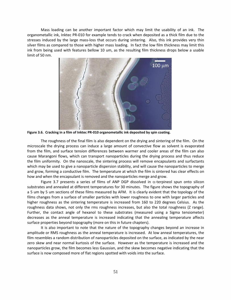
51
Mass loading can be another important factor which may limit the usability of an ink. The organometallic ink, Inktec PR-010 for example tends to crack when deposited as a thick film due to the stresses induced by the large mass-loss that occurs during sintering. Also, this ink provides very thin silver films as compared to those with higher mass loading. In fact the low film thickness may limit this ink from being used with features bellow 10 um, as the resulting film thickness drops below a usable limit of 50 nm.
Figure 3.6. Cracking in a film of Inktec PR-010 organometallic ink deposited by spin coating.
The roughness of the final film is also dependent on the drying and sintering of the film. On the microscale the drying process can induce a large amount of convective flow as solvent is evaporated from the film, and surface tension differences between warmer and cooler areas of the film can also cause Marangoni flows, which can transport nanoparticles during the drying process and thus reduce the film uniformity. On the nanoscale, the sintering process will remove encapsulants and surfactants which may be used to give a nanoparticle dispersion stability, and will cause the nanoparticles to merge and grow, forming a conductive film. The temperature at which the film is sintered has clear effects on how and when the encapsulant is removed and the nanoparticles merge and grow.
Figure 3.7 presents a series of films of ANP DGP dissolved in -terpineol spun onto silicon substrates and annealed at different temperatures for 30 minutes. The figure shows the topography of a 5 um by 5 um sections of these films measured by AFM. It is clearly evident that the topology of the films changes from a surface of smaller particles with lower roughness to one with larger particles and higher roughness as the sintering temperature is increased from 160 to 220 degrees Celsius. As the roughness data shows, not only the rms roughness increases, but also the total roughness (Z range). Further, the contact angle of hexanol to these substrates (measured using a Sigma tensiometer) decreases as the anneal temperature is increased indicating that the annealing temperature affects surface properties beyond topography (more on this in future chapters). It is also important to note that the nature of the topography changes beyond an increase in amplitude or RMS roughness as the anneal temperature is increased. At low anneal temperatures, the film resembles a random distribution of nanoparticles deposited on the surface, as indicated by the near zero skew and near normal kurtosis of the surface. However as the temperature is increased and the nanoparticles grow, the film becomes less Gaussian, and the skew becomes negative indicating that the surface is now composed more of flat regions spotted with voids into the surface.
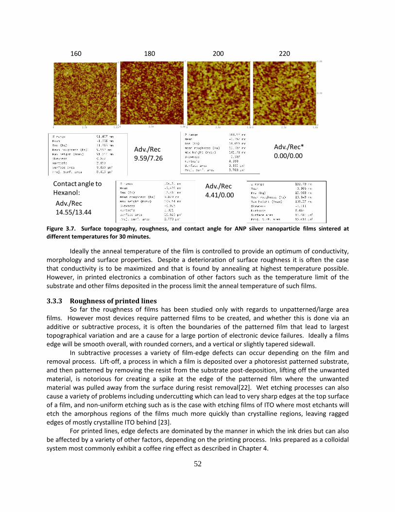
52
Figure 3.7. Surface topography, roughness, and contact angle for ANP silver nanoparticle films sintered at different temperatures for 30 minutes.
Ideally the anneal temperature of the film is controlled to provide an optimum of conductivity, morphology and surface properties. Despite a deterioration of surface roughness it is often the case that conductivity is to be maximized and that is found by annealing at highest temperature possible. However, in printed electronics a combination of other factors such as the temperature limit of the substrate and other films deposited in the process limit the anneal temperature of such films.
3.3.3 Roughness of printed lines So far the roughness of films has been studied only with regards to unpatterned/large area films. However most devices require patterned films to be created, and whether this is done via an additive or subtractive process, it is often the boundaries of the patterned film that lead to largest topographical variation and are a cause for a large portion of electronic device failures. Ideally a films edge will be smooth overall, with rounded corners, and a vertical or slightly tapered sidewall. In subtractive processes a variety of film-edge defects can occur depending on the film and removal process. Lift-off, a process in which a film is deposited over a photoresist patterned substrate, and then patterned by removing the resist from the substrate post-deposition, lifting off the unwanted material, is notorious for creating a spike at the edge of the patterned film where the unwanted material was pulled away from the surface during resist removal[22]. Wet etching processes can also cause a variety of problems including undercutting which can lead to very sharp edges at the top surface of a film, and non-uniform etching such as is the case with etching films of ITO where most etchants will etch the amorphous regions of the films much more quickly than crystalline regions, leaving ragged edges of mostly crystalline ITO behind [23]. For printed lines, edge defects are dominated by the manner in which the ink dries but can also be affected by a variety of other factors, depending on the printing process. Inks prepared as a colloidal system most commonly exhibit a coffee ring effect as described in Chapter 4.
160 180 200 220
Adv./Rec14.55/13.44
Adv./Rec9.59/7.26
Adv./Rec4.41/0.00
Adv./Rec*0.00/0.00
Contact angle to Hexanol:

53
In some cases, the convective flow that causes the coffee ring can be so strong that all material is removed from the center of the drop yielding a non-conductive area in the center of the line as shown in Figure 3.8. Such a line would yield a capacitor with lower than expected capacitance, an LED with low brightness or a TFT with low to no on current. Further, the spikes at the edges of the line would create a large susceptibility to shorting failures.
Figure 3.8. AFM topography of a gold nanoparticle line showing significant coffee ring drying.
In colloidal systems the coffee ring can be avoided by a variety of approaches. One approach is to design an ink with significant Marangoni flow. Marangoni flow is caused by a difference in surface tension due to a temperature gradient. In the case of a drying drop, the top of the drop is at a lower temperature than the edge of the drop. This difference in surface tension causes the fluid from the edge of the drop to be pulled in to the center of the drop, thus moving material back towards the center of the drop [24]. An ink formulation which exhibits this type of Marangoni flow should have a relatively high contact angle to the substrate to avoid resistively limiting the flow, and should be fairly unsusceptible to contamination which may locally change the surface tension of the drop. Since formulating such an ink is sometime difficult, an approach that drives the marangoni flow by using multiple solvents has been developed [25]. The strategy is to combine a solvent with a higher boiling point but lower surface tension than the main solvent so that a concentration gradient is formed where the higher boiling point solvent is a higher percentage of the fluid near the edge of the drop where evaporation is highest thus giving the edge of the droplet a smaller surface tension than the center, inducing a strong Marangoni flow. By adjusting the concentrations of the solvents, the strength of the Marangoni flow can be optimized to minimize the effects of the convective flow due to evaporation. Other possibilities for reducing the coffee ring in colloidal systems are to reduce the time to gel of the ink, or eliminate contact line pinning [26]. Increasing the concentration of nanoparticles, or the viscosity of the ink can lead to a point where it will quickly gel upon deposition, resisting convective flows. This can be seen most commonly in high viscosity inks developed for screen printing or gravure. Eliminating contact line pining would allow the drop to contract until the solvent has been entirely removed. This however requires using substrates of low surface energy, which can make it difficult to form stable lines. Organometallic based inks suffer much less from coffee ring effects. They are solute/solvent systems where the organometallic solute has a high diffusivity in the solvent and can thus redistribute quickly as the solvent evaporates. Further these systems are less prone to contact line pinning and the solute can flow well near the contact line, unlike nanoparticles which can get stuck between the
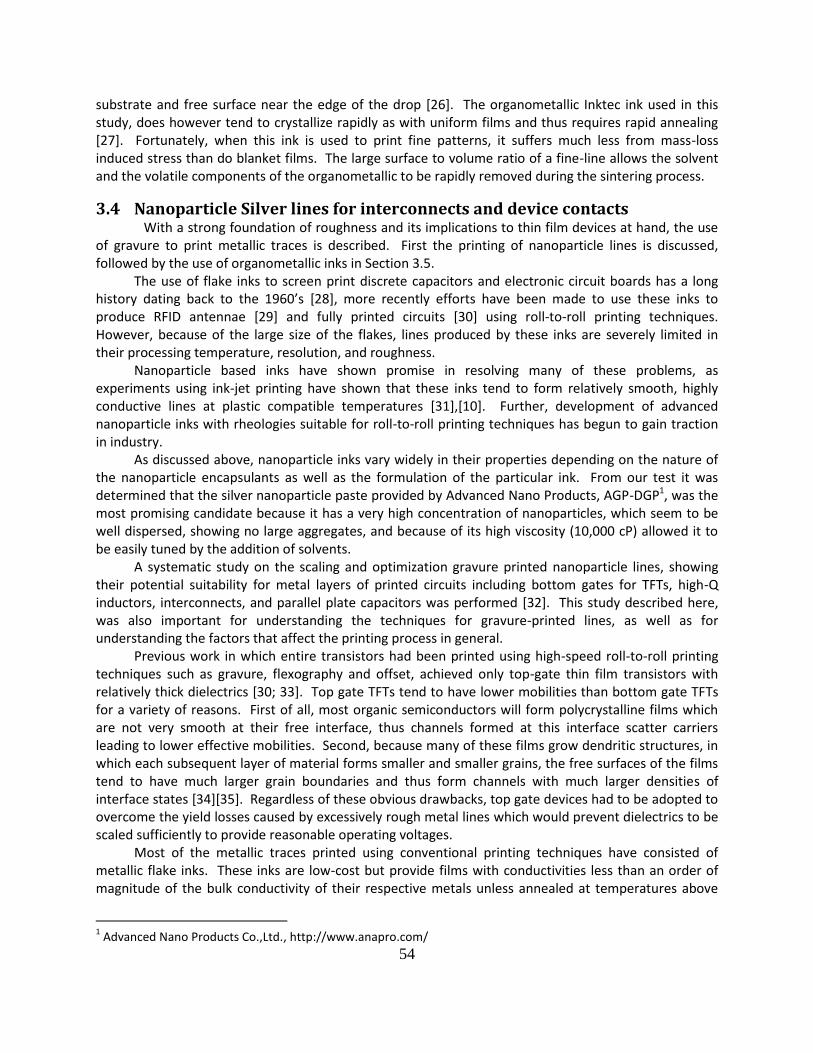
54
substrate and free surface near the edge of the drop [26]. The organometallic Inktec ink used in this study, does however tend to crystallize rapidly as with uniform films and thus requires rapid annealing [27]. Fortunately, when this ink is used to print fine patterns, it suffers much less from mass-loss induced stress than do blanket films. The large surface to volume ratio of a fine-line allows the solvent and the volatile components of the organometallic to be rapidly removed during the sintering process.
3.4 Nanoparticle Silver lines for interconnects and device contacts With a strong foundation of roughness and its implications to thin film devices at hand, the use of gravure to print metallic traces is described. First the printing of nanoparticle lines is discussed, followed by the use of organometallic inks in Section 3.5.
The use of flake inks to screen print discrete capacitors and electronic circuit boards has a long history dating back to the 1960’s [28], more recently efforts have been made to use these inks to produce RFID antennae [29] and fully printed circuits [30] using roll-to-roll printing techniques. However, because of the large size of the flakes, lines produced by these inks are severely limited in their processing temperature, resolution, and roughness.
Nanoparticle based inks have shown promise in resolving many of these problems, as experiments using ink-jet printing have shown that these inks tend to form relatively smooth, highly conductive lines at plastic compatible temperatures [31],[10]. Further, development of advanced nanoparticle inks with rheologies suitable for roll-to-roll printing techniques has begun to gain traction in industry.
As discussed above, nanoparticle inks vary widely in their properties depending on the nature of the nanoparticle encapsulants as well as the formulation of the particular ink. From our test it was determined that the silver nanoparticle paste provided by Advanced Nano Products, AGP-DGP1, was the most promising candidate because it has a very high concentration of nanoparticles, which seem to be well dispersed, showing no large aggregates, and because of its high viscosity (10,000 cP) allowed it to be easily tuned by the addition of solvents.
A systematic study on the scaling and optimization gravure printed nanoparticle lines, showing their potential suitability for metal layers of printed circuits including bottom gates for TFTs, high-Q inductors, interconnects, and parallel plate capacitors was performed [32]. This study described here, was also important for understanding the techniques for gravure-printed lines, as well as for understanding the factors that affect the printing process in general.
Previous work in which entire transistors had been printed using high-speed roll-to-roll printing techniques such as gravure, flexography and offset, achieved only top-gate thin film transistors with relatively thick dielectrics [30; 33]. Top gate TFTs tend to have lower mobilities than bottom gate TFTs for a variety of reasons. First of all, most organic semiconductors will form polycrystalline films which are not very smooth at their free interface, thus channels formed at this interface scatter carriers leading to lower effective mobilities. Second, because many of these films grow dendritic structures, in which each subsequent layer of material forms smaller and smaller grains, the free surfaces of the films tend to have much larger grain boundaries and thus form channels with much larger densities of interface states [34][35]. Regardless of these obvious drawbacks, top gate devices had to be adopted to overcome the yield losses caused by excessively rough metal lines which would prevent dielectrics to be scaled sufficiently to provide reasonable operating voltages.
Most of the metallic traces printed using conventional printing techniques have consisted of metallic flake inks. These inks are low-cost but provide films with conductivities less than an order of magnitude of the bulk conductivity of their respective metals unless annealed at temperatures above
1 Advanced Nano Products Co.,Ltd., http://www.anapro.com/

55
400° C, and because of the size of their flakes, provide films with roughness on the order of microns and similar minimum film thicknesses.
Nanoparticle inks offer clear benefits to flake inks for printed electronics because they can achieve high conductivities similar to their bulk metals at plastic compatible (<200degC) sintering temperatures [10]. They can provide films with nanometer scale roughness and can provide conductive films with thicknesses as low as 50nm, equivalent to only a layer or two of nanoparticles.
The goal of this study was to lay the groundwork for further studies on gravure printed electronics establishing basic rheological principles and demonstrating the viability and scalability of the gravure printing process. As mentioned, there have been a number of studies on various aspects of gravure including the fluid emptying process, as well as coating quality as a function of various operating parameters. These studies, however, have used very large cells, model inks, and have not focused on the properties of printed features of most interest to electronics.
This work, on the other hand, uses a variety of cell sizes beginning from sizes commonly used in industry to the smallest cells available at this time; and using the appropriate inks, focuses on the scaling and optimization of conductive lines. The use of intaglio and gravure features is compared and used to determine which is best for printing uniform, narrow lines. Several qualitative and quantitative trends are presented by varying cell widths, cell depths, and ink parameters, and the challenges in further scaling the minimum achievable line widths is discussed.
3.4.1 Experimental Printing tests were performed on our custom-built gravure printer using two types of gravure
cylinders, each with a variety of cell widths and depths. One cylinder was patterned by photolithography whereby the roll was blade coated with a photoresist, then covered with a flexible patterned chrome mask, exposed to UV light through a slit, developed, and finally wet etched in a FeCl solution before being chrome coated. Another cylinder was patterned using the indirect laser method whereby a photoresist is patterned by laser writing, developed, and etched as above, followed by chrome coating. The wet etching process used in fabricating these rolls is an isotropic one, yielding wells with hemispherical shapes, which generally for a given well width provides more volume than comparable cell patterned by diamond indentation. The anisotropic behavior of the etch chemistry limits the achievable aspect ratio especially for well widths below 40 um where sidewall etching becomes a significant portion of the final well width thus constraining the cell dimensions used in this study.
Figure 3.9. Three different cell configurations used to study printing properties of nanoparticle inks.
Images of individual cells, gravure lines, and intaglio lines are presented in Figure 3.9. Individual dots are used to study the effects of cell emptying. Lines printed from gravure patterns with various cell sizes and spacings are compared to those formed by intaglio patterns with various widths and depths. The test cylinders contain well widths between 10 and 64 microns and cell depths between 4 and 19 microns.
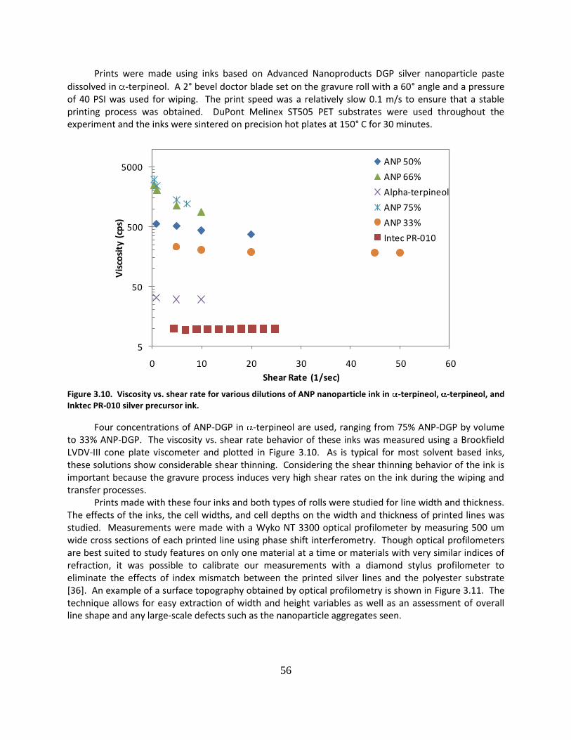
56
Prints were made using inks based on Advanced Nanoproducts DGP silver nanoparticle paste
dissolved in -terpineol. A 2° bevel doctor blade set on the gravure roll with a 60° angle and a pressure of 40 PSI was used for wiping. The print speed was a relatively slow 0.1 m/s to ensure that a stable printing process was obtained. DuPont Melinex ST505 PET substrates were used throughout the experiment and the inks were sintered on precision hot plates at 150° C for 30 minutes.
5
50
500
5000
0 10 20 30 40 50 60
Vis
cosi
ty (
cps)
Shear Rate (1/sec)
ANP 50%
ANP 66%
Alpha-terpineol
ANP 75%
ANP 33%
Intec PR-010
Figure 3.10. Viscosity vs. shear rate for various dilutions of ANP nanoparticle ink in -terpineol, -terpineol, and Inktec PR-010 silver precursor ink.
Four concentrations of ANP-DGP in -terpineol are used, ranging from 75% ANP-DGP by volume to 33% ANP-DGP. The viscosity vs. shear rate behavior of these inks was measured using a Brookfield LVDV-III cone plate viscometer and plotted in Figure 3.10. As is typical for most solvent based inks, these solutions show considerable shear thinning. Considering the shear thinning behavior of the ink is important because the gravure process induces very high shear rates on the ink during the wiping and transfer processes.
Prints made with these four inks and both types of rolls were studied for line width and thickness. The effects of the inks, the cell widths, and cell depths on the width and thickness of printed lines was studied. Measurements were made with a Wyko NT 3300 optical profilometer by measuring 500 um wide cross sections of each printed line using phase shift interferometry. Though optical profilometers are best suited to study features on only one material at a time or materials with very similar indices of refraction, it was possible to calibrate our measurements with a diamond stylus profilometer to eliminate the effects of index mismatch between the printed silver lines and the polyester substrate [36]. An example of a surface topography obtained by optical profilometry is shown in Figure 3.11. The technique allows for easy extraction of width and height variables as well as an assessment of overall line shape and any large-scale defects such as the nanoparticle aggregates seen.
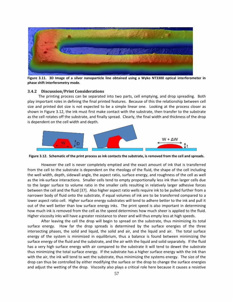
57
Figure 3.11. 3D Image of a silver nanoparticle line obtained using a Wyko NT3300 optical interferometer in phase shift interferometry mode.
3.4.2 Discussion/Print Considerations The printing process can be separated into two parts, cell emptying, and drop spreading. Both
play important roles in defining the final printed features. Because of this the relationship between cell size and printed dot size is not expected to be a simple linear one. Looking at the process closer as shown in Figure 3.12, the ink must first make contact with the substrate, then transfer to the substrate as the cell rotates off the substrate, and finally spread. Clearly, the final width and thickness of the drop is dependent on the cell width and depth.
Figure 3.12. Schematic of the print process as ink contacts the substrate, is removed from the cell and spreads.
However the cell is never completely emptied and the exact amount of ink that is transferred from the cell to the substrate is dependent on the rheology of the fluid, the shape of the cell including the well width, depth, sidewall angle, the aspect ratio, surface energy, and roughness of the cell as well as the ink-surface interactions. Smaller cells tend to empty proportionally less ink than larger cells due to the larger surface to volume ratio in the smaller cells resulting in relatively larger adhesive forces between the cell and the fluid [37]. Also higher aspect ratio wells require ink to be pulled further from a narrower body of fluid onto the substrate, if equal volumes of ink are to be transferred compared to a lower aspect ratio cell. Higher surface energy substrates will tend to adhere better to the ink and pull it out of the well better than low surface energy inks. The print speed is also important in determining how much ink is removed from the cell as the speed determines how much sheer is applied to the fluid. Higher viscosity inks will have a greater resistance to sheer and will thus empty less at high speeds. After leaving the cell the drop will begin to spread on the substrate, thus minimizing its total surface energy. How far the drop spreads is determined by the surface energies of the three intersecting phases, the solid and liquid, the solid and air, and the liquid and air. The total surface energy of the system is minimized in equilibrium, thus a balance is found between minimizing the surface energy of the fluid and the substrate, and the air with the liquid and solid separately. If the fluid has a very high surface energy with air compared to the substrate it will tend to dewet the substrate thus minimizing the total surface energy. If the substrate has a higher surface energy with the ink than with the air, the ink will tend to wet the substrate, thus minimizing the systems energy. The size of the drop can thus be controlled by either modifying the surface or the drop to change the surface energies and adjust the wetting of the drop. Viscosity also plays a critical role here because it causes a resistive

58
drag, slowing the motion of the drop and thus perhaps preventing it from reaching equilibrium before the drop dries. A low viscosity ink, on the other hand may lead to poor pattern definition causing the drop to “bleed out” or “splash” out of the cell reducing pattern fidelity. Line formation happens when drops are deposited close together and thus coalesce as they spread on the substrate. Line formation has been well studied for ink-jet printing [38][39] and it has been shown that a variety of regimes of line behavior can be found. Three primary regimes can be distinguished: drops placed far apart will remain individual dots; as the drop spacing decreases the drops intersect forming a wavy edged, or scalloped line; as the drop spacing decreases further, drops begin to merge and form a smooth continuous line. There is thus an optimal drop spacing that provides the smoothest and most uniform lines. With these inks it is determined that optimal lines can be formed with a drop cell spacing to cell width ratio between 1.06 and 1.4. If this ratio is much larger than 1.4, then scalloped lines will be produced. Here drop cell spacing is considered center-to-center. Viscosity plays another important role in achieving good lines. If the ink is too viscous, drops will not flow smoothly into each other and resulting lines will have poor width and thickness uniformity. On the other hand if the ink viscosity is too low the ink will provide lines that are too thin to be conductive. Thus the optimal ink viscosity will provide thin, smooth, straight lines with maximum printed thickness. Thicker lines will tend to provide more uniform print thickness because they allow more time for capillary flow, smoothing the surfaces of the individual drops.
3.4.3 Results With these considerations in mind the prints made with various ANP-DGP nanoparticle inks will be discussed presenting qualitative and quantitative behavioral trends which are useful for understanding the printing process and for optimizing and scaling printed lines. The printing behavior of individual dots will be discussed first, identifying relationships between the cell and ink parameters on the print. The optimal ink dilution will be revealed through this work. Then prints from patterns of closely spaced gravure cells will be compared to those formed form intaglio trenches. Finally the minimum line widths achieved are presented along with a discussion of the challenges to further scaling.
3.4.3.1 Individual Dots Printing individual dots allows for the study of ink transfer mechanism and drop spreading
without combining interactions of other drops or effects of cell emptying for adjacent cells. An interesting phenomena readily obtained is the formation of “doughnuts” which are printed dots with an empty space in the middle. As can be seen in Figure 3.13 the left image shows dots formed by a roll with very shallow wells (low aspect ratio). In this case there is insufficient ink in the well to fully fill the dot. When the cell rotates over the substrate, ink is first drawn out of the well at the leading edge of the cell, then around the edge of the cell as the cell rotates over the substrate, leaving the center of the cell depleted of ink, and thus forming the characteristic print. As shown below, the print width will scale linearly with the cell width irrespective of the aspect ratio, but experimental data shows that cell aspect ratio- the cell depth to cell width- must be larger than 1/7 or 1/8 to avoid doughnuts.
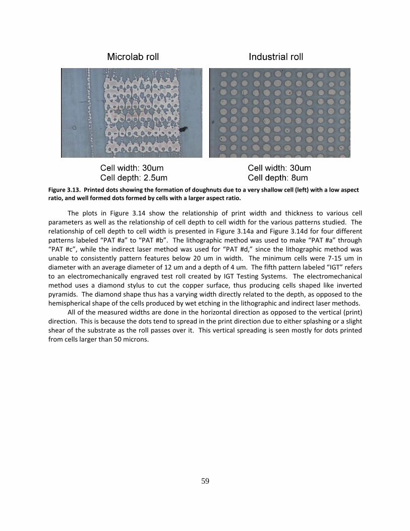
59
Figure 3.13. Printed dots showing the formation of doughnuts due to a very shallow cell (left) with a low aspect ratio, and well formed dots formed by cells with a larger aspect ratio.
The plots in Figure 3.14 show the relationship of print width and thickness to various cell parameters as well as the relationship of cell depth to cell width for the various patterns studied. The relationship of cell depth to cell width is presented in Figure 3.14a and Figure 3.14d for four different patterns labeled “PAT #a” to “PAT #b”. The lithographic method was used to make “PAT #a” through “PAT #c”, while the indirect laser method was used for “PAT #d,” since the lithographic method was unable to consistently pattern features below 20 um in width. The minimum cells were 7-15 um in diameter with an average diameter of 12 um and a depth of 4 um. The fifth pattern labeled “IGT” refers to an electromechanically engraved test roll created by IGT Testing Systems. The electromechanical method uses a diamond stylus to cut the copper surface, thus producing cells shaped like inverted pyramids. The diamond shape thus has a varying width directly related to the depth, as opposed to the hemispherical shape of the cells produced by wet etching in the lithographic and indirect laser methods.
All of the measured widths are done in the horizontal direction as opposed to the vertical (print) direction. This is because the dots tend to spread in the print direction due to either splashing or a slight shear of the substrate as the roll passes over it. This vertical spreading is seen mostly for dots printed from cells larger than 50 microns.
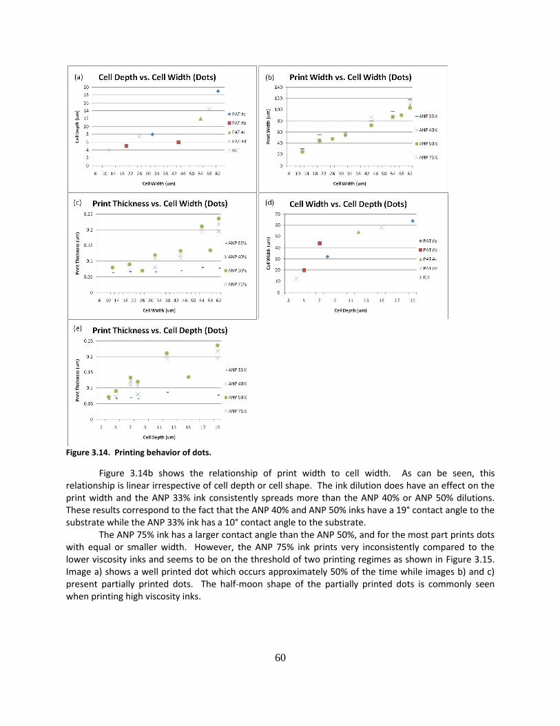
60
Figure 3.14. Printing behavior of dots.
Figure 3.14b shows the relationship of print width to cell width. As can be seen, this relationship is linear irrespective of cell depth or cell shape. The ink dilution does have an effect on the print width and the ANP 33% ink consistently spreads more than the ANP 40% or ANP 50% dilutions. These results correspond to the fact that the ANP 40% and ANP 50% inks have a 19° contact angle to the substrate while the ANP 33% ink has a 10° contact angle to the substrate. The ANP 75% ink has a larger contact angle than the ANP 50%, and for the most part prints dots with equal or smaller width. However, the ANP 75% ink prints very inconsistently compared to the lower viscosity inks and seems to be on the threshold of two printing regimes as shown in Figure 3.15. Image a) shows a well printed dot which occurs approximately 50% of the time while images b) and c) present partially printed dots. The half-moon shape of the partially printed dots is commonly seen when printing high viscosity inks.
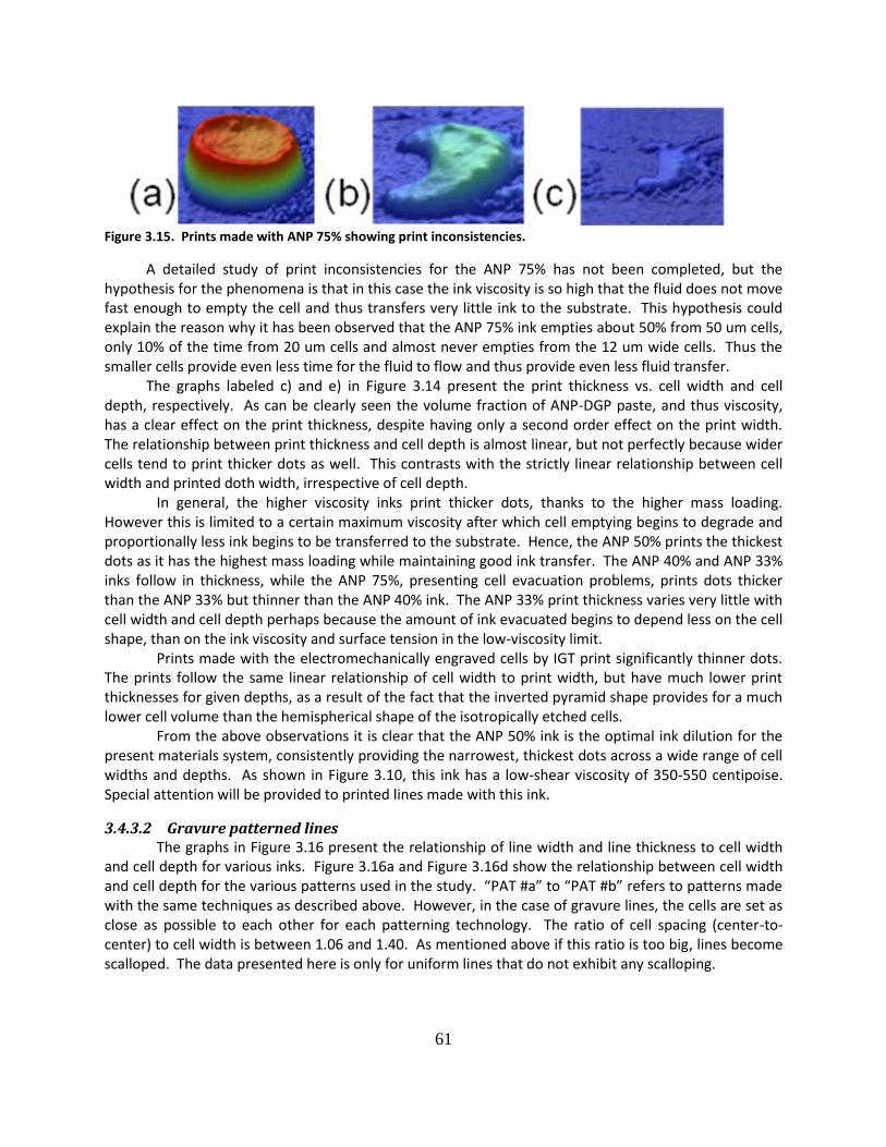
61
Figure 3.15. Prints made with ANP 75% showing print inconsistencies.
A detailed study of print inconsistencies for the ANP 75% has not been completed, but the hypothesis for the phenomena is that in this case the ink viscosity is so high that the fluid does not move fast enough to empty the cell and thus transfers very little ink to the substrate. This hypothesis could explain the reason why it has been observed that the ANP 75% ink empties about 50% from 50 um cells, only 10% of the time from 20 um cells and almost never empties from the 12 um wide cells. Thus the smaller cells provide even less time for the fluid to flow and thus provide even less fluid transfer.
The graphs labeled c) and e) in Figure 3.14 present the print thickness vs. cell width and cell depth, respectively. As can be clearly seen the volume fraction of ANP-DGP paste, and thus viscosity, has a clear effect on the print thickness, despite having only a second order effect on the print width. The relationship between print thickness and cell depth is almost linear, but not perfectly because wider cells tend to print thicker dots as well. This contrasts with the strictly linear relationship between cell width and printed doth width, irrespective of cell depth. In general, the higher viscosity inks print thicker dots, thanks to the higher mass loading. However this is limited to a certain maximum viscosity after which cell emptying begins to degrade and proportionally less ink begins to be transferred to the substrate. Hence, the ANP 50% prints the thickest dots as it has the highest mass loading while maintaining good ink transfer. The ANP 40% and ANP 33% inks follow in thickness, while the ANP 75%, presenting cell evacuation problems, prints dots thicker than the ANP 33% but thinner than the ANP 40% ink. The ANP 33% print thickness varies very little with cell width and cell depth perhaps because the amount of ink evacuated begins to depend less on the cell shape, than on the ink viscosity and surface tension in the low-viscosity limit. Prints made with the electromechanically engraved cells by IGT print significantly thinner dots. The prints follow the same linear relationship of cell width to print width, but have much lower print thicknesses for given depths, as a result of the fact that the inverted pyramid shape provides for a much lower cell volume than the hemispherical shape of the isotropically etched cells. From the above observations it is clear that the ANP 50% ink is the optimal ink dilution for the present materials system, consistently providing the narrowest, thickest dots across a wide range of cell widths and depths. As shown in Figure 3.10, this ink has a low-shear viscosity of 350-550 centipoise. Special attention will be provided to printed lines made with this ink.
3.4.3.2 Gravure patterned lines The graphs in Figure 3.16 present the relationship of line width and line thickness to cell width
and cell depth for various inks. Figure 3.16a and Figure 3.16d show the relationship between cell width and cell depth for the various patterns used in the study. “PAT #a” to “PAT #b” refers to patterns made with the same techniques as described above. However, in the case of gravure lines, the cells are set as close as possible to each other for each patterning technology. The ratio of cell spacing (center-to-center) to cell width is between 1.06 and 1.40. As mentioned above if this ratio is too big, lines become scalloped. The data presented here is only for uniform lines that do not exhibit any scalloping.
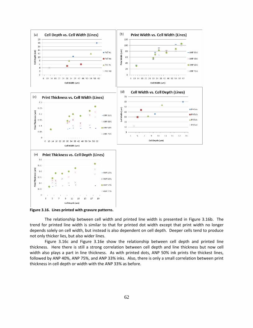
62
Figure 3.16. Lines printed with gravure patterns.
The relationship between cell width and printed line width is presented in Figure 3.16b. The trend for printed line width is similar to that for printed dot width except that print width no longer depends solely on cell width, but instead is also dependent on cell depth. Deeper cells tend to produce not only thicker lies, but also wider lines. Figure 3.16c and Figure 3.16e show the relationship between cell depth and printed line thickness. Here there is still a strong correlation between cell depth and line thickness but now cell width also plays a part in line thickness. As with printed dots, ANP 50% ink prints the thickest lines, followed by ANP 40%, ANP 75%, and ANP 33% inks. Also, there is only a small correlation between print thickness in cell depth or width with the ANP 33% as before.
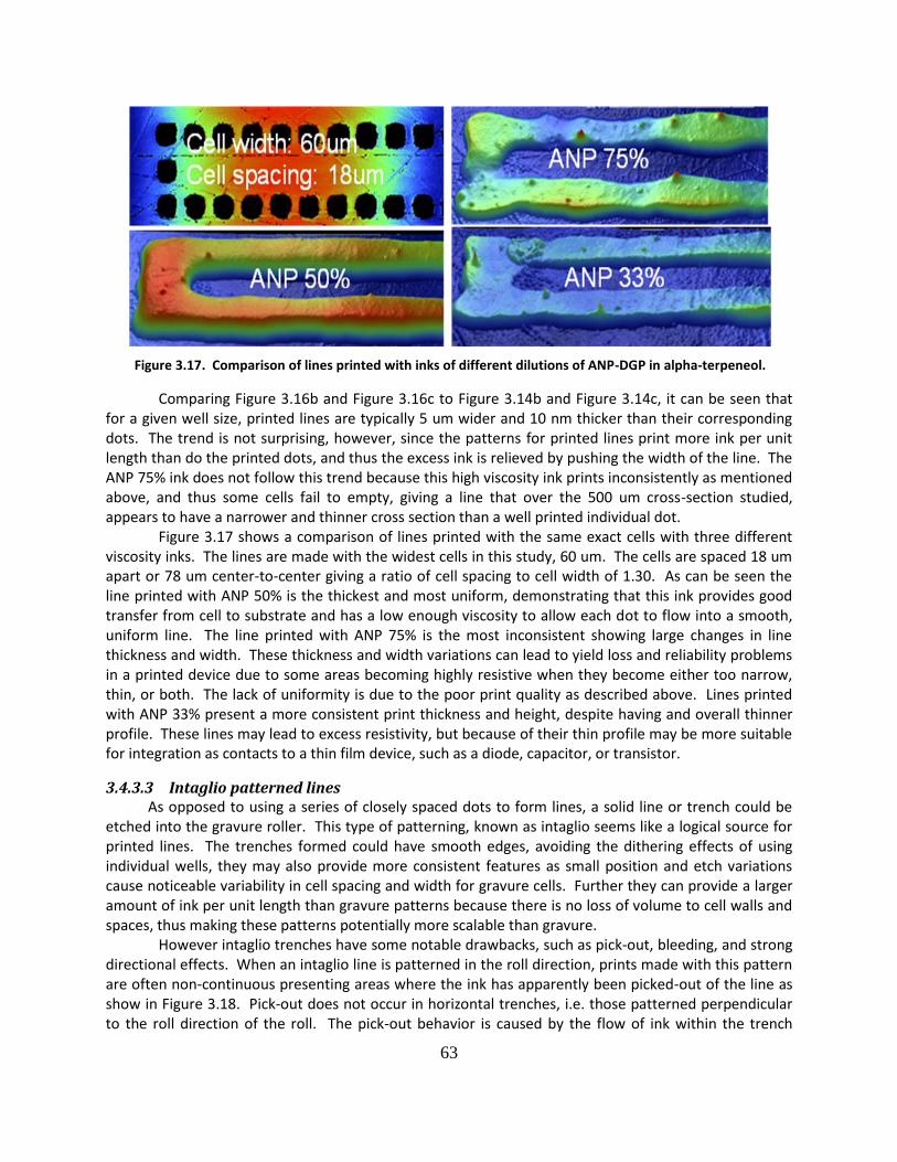
63
Comparing Figure 3.16b and Figure 3.16c to Figure 3.14b and Figure 3.14c, it can be seen that for a given well size, printed lines are typically 5 um wider and 10 nm thicker than their corresponding dots. The trend is not surprising, however, since the patterns for printed lines print more ink per unit length than do the printed dots, and thus the excess ink is relieved by pushing the width of the line. The ANP 75% ink does not follow this trend because this high viscosity ink prints inconsistently as mentioned above, and thus some cells fail to empty, giving a line that over the 500 um cross-section studied, appears to have a narrower and thinner cross section than a well printed individual dot. Figure 3.17 shows a comparison of lines printed with the same exact cells with three different viscosity inks. The lines are made with the widest cells in this study, 60 um. The cells are spaced 18 um apart or 78 um center-to-center giving a ratio of cell spacing to cell width of 1.30. As can be seen the line printed with ANP 50% is the thickest and most uniform, demonstrating that this ink provides good transfer from cell to substrate and has a low enough viscosity to allow each dot to flow into a smooth, uniform line. The line printed with ANP 75% is the most inconsistent showing large changes in line thickness and width. These thickness and width variations can lead to yield loss and reliability problems in a printed device due to some areas becoming highly resistive when they become either too narrow, thin, or both. The lack of uniformity is due to the poor print quality as described above. Lines printed with ANP 33% present a more consistent print thickness and height, despite having and overall thinner profile. These lines may lead to excess resistivity, but because of their thin profile may be more suitable for integration as contacts to a thin film device, such as a diode, capacitor, or transistor.
3.4.3.3 Intaglio patterned lines As opposed to using a series of closely spaced dots to form lines, a solid line or trench could be
etched into the gravure roller. This type of patterning, known as intaglio seems like a logical source for printed lines. The trenches formed could have smooth edges, avoiding the dithering effects of using individual wells, they may also provide more consistent features as small position and etch variations cause noticeable variability in cell spacing and width for gravure cells. Further they can provide a larger amount of ink per unit length than gravure patterns because there is no loss of volume to cell walls and spaces, thus making these patterns potentially more scalable than gravure. However intaglio trenches have some notable drawbacks, such as pick-out, bleeding, and strong directional effects. When an intaglio line is patterned in the roll direction, prints made with this pattern are often non-continuous presenting areas where the ink has apparently been picked-out of the line as show in Figure 3.18. Pick-out does not occur in horizontal trenches, i.e. those patterned perpendicular to the roll direction of the roll. The pick-out behavior is caused by the flow of ink within the trench
Figure 3.17. Comparison of lines printed with inks of different dilutions of ANP-DGP in alpha-terpeneol.
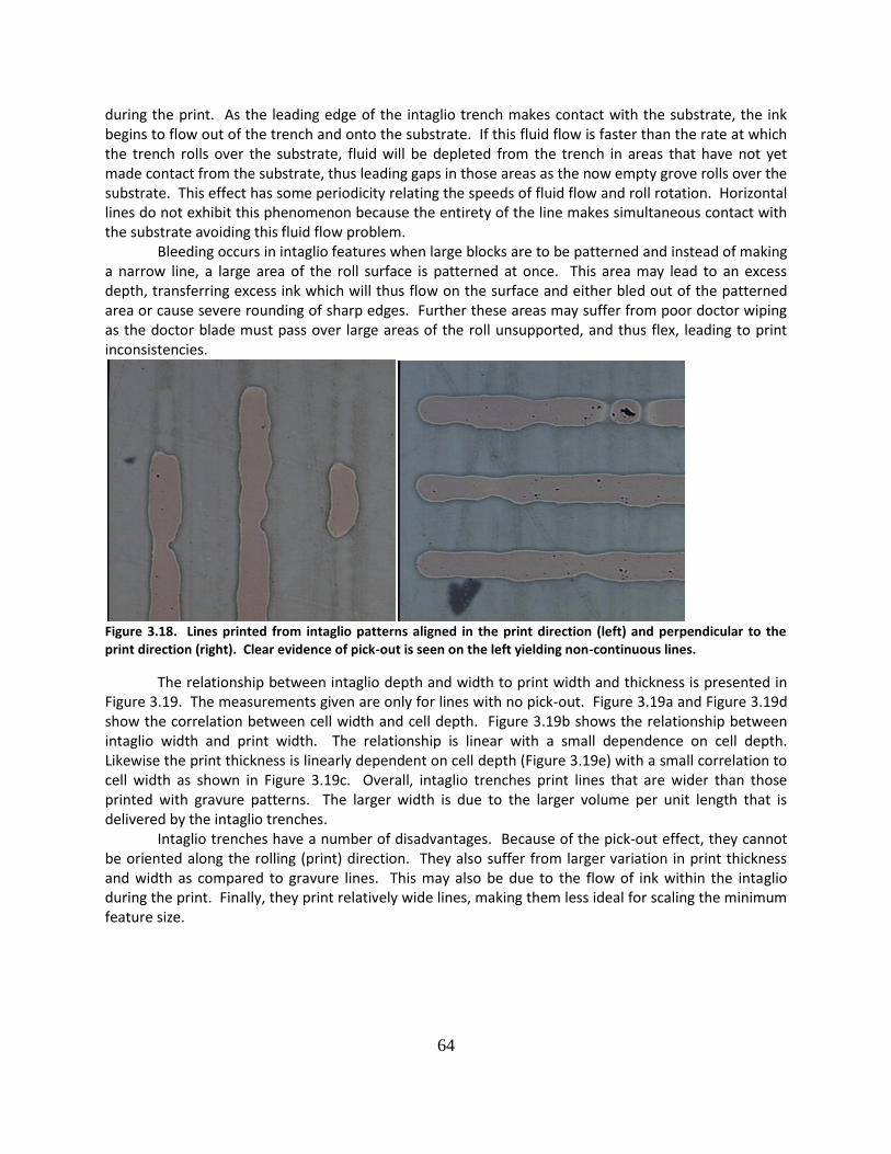
64
during the print. As the leading edge of the intaglio trench makes contact with the substrate, the ink begins to flow out of the trench and onto the substrate. If this fluid flow is faster than the rate at which the trench rolls over the substrate, fluid will be depleted from the trench in areas that have not yet made contact from the substrate, thus leading gaps in those areas as the now empty grove rolls over the substrate. This effect has some periodicity relating the speeds of fluid flow and roll rotation. Horizontal lines do not exhibit this phenomenon because the entirety of the line makes simultaneous contact with the substrate avoiding this fluid flow problem. Bleeding occurs in intaglio features when large blocks are to be patterned and instead of making a narrow line, a large area of the roll surface is patterned at once. This area may lead to an excess depth, transferring excess ink which will thus flow on the surface and either bled out of the patterned area or cause severe rounding of sharp edges. Further these areas may suffer from poor doctor wiping as the doctor blade must pass over large areas of the roll unsupported, and thus flex, leading to print inconsistencies.
Figure 3.18. Lines printed from intaglio patterns aligned in the print direction (left) and perpendicular to the print direction (right). Clear evidence of pick-out is seen on the left yielding non-continuous lines.
The relationship between intaglio depth and width to print width and thickness is presented in Figure 3.19. The measurements given are only for lines with no pick-out. Figure 3.19a and Figure 3.19d show the correlation between cell width and cell depth. Figure 3.19b shows the relationship between intaglio width and print width. The relationship is linear with a small dependence on cell depth. Likewise the print thickness is linearly dependent on cell depth (Figure 3.19e) with a small correlation to cell width as shown in Figure 3.19c. Overall, intaglio trenches print lines that are wider than those printed with gravure patterns. The larger width is due to the larger volume per unit length that is delivered by the intaglio trenches. Intaglio trenches have a number of disadvantages. Because of the pick-out effect, they cannot be oriented along the rolling (print) direction. They also suffer from larger variation in print thickness and width as compared to gravure lines. This may also be due to the flow of ink within the intaglio during the print. Finally, they print relatively wide lines, making them less ideal for scaling the minimum feature size.
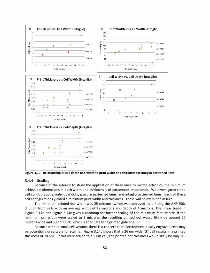
65
Figure 3.19. Relationship of cell depth and width to print width and thickness for intaglio patterned lines.
3.4.4 Scaling Because of the interest to study the application of these lines to microelectronics, the minimum
achievable dimensions in both width and thickness is of paramount importance. We investigated three cell configurations: individual dots, gravure patterned lines, and intaglio patterned lines. Each of these cell configurations yielded a minimum print width and thickness. These will be examined in turn.
The minimum printed dot width was 25 microns, which was achieved by printing the ANP 50% dilution from cells with an average width of 12 microns and depth of 4 microns. The linear trend in Figure 3.14b and Figure 3.14c gives a roadmap for further scaling of the minimum feature size. If the minimum cell width were scaled to 5 microns, the resulting printed dot would likely be around 20 microns wide and 50 nm thick, which is adequate for a printed gate line.
Because of their small cell volume, there is a concern that electromechanically engraved cells may be potentially unsuitable for scaling. Figure 3.14c shows that a 26 um wide IGT cell results in a printed thickness of 70 nm. If this were scaled to a 5 um cell, the printed dot thickness would likely be only 20-
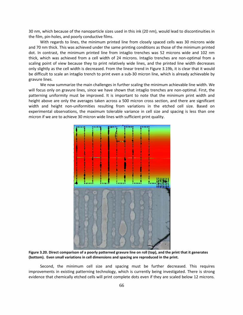
66
30 nm, which because of the nanoparticle sizes used in this ink (20 nm), would lead to discontinuities in the film, pin-holes, and poorly conductive films.
With regards to lines, the minimum printed line from closely spaced cells was 30 microns wide and 70 nm thick. This was achieved under the same printing conditions as those of the minimum printed dot. In contrast, the minimum printed line from intaglio trenches was 52 microns wide and 102 nm thick, which was achieved from a cell width of 24 microns. Intaglio trenches are non-optimal from a scaling point of view because they to print relatively wide lines, and the printed line width decreases only slightly as the cell width is decreased. From the linear trend in Figure 3.19b, it is clear that it would be difficult to scale an intaglio trench to print even a sub-30 micron line, which is already achievable by gravure lines.
We now summarize the main challenges in further scaling the minimum achievable line width. We will focus only on gravure lines, since we have shown that intaglio trenches are non-optimal. First, the patterning uniformity must be improved. It is important to note that the minimum print width and height above are only the averages taken across a 500 micron cross section, and there are significant width and height non-uniformities resulting from variations in the etched cell size. Based on experimental observations, the maximum tolerable variance in cell size and spacing is less than one micron if we are to achieve 30 micron wide lines with sufficient print quality.
Figure 3.20. Direct comparison of a poorly patterned gravure line on roll (top), and the print that it generates (bottom). Even small variations in cell dimensions and spacing are reproduced in the print.
Second, the minimum cell size and spacing must be further decreased. This requires improvements in existing patterning technology, which is currently being investigated. There is strong evidence that chemically etched cells will print complete dots even if they are scaled below 12 microns.
67
As shown in Figure 3.20, printed lines strongly track cell defects and non-uniformities, even when some of the cells are as small as 7 microns wide. This suggests that such small features will indeed be imaged if appropriate cell sizes and volumes are produced. This is consistent with the scaling predictions discussed previously. This image was printed using the ANP 50% ink using the smallest size wells in our experiment.
An alternative route for scaling the minimum feature size is to change to a different ink or substrate. With our material system, the print width is nearly 2-3 times larger than the cell width for almost every cell. This spreading can possibly be reduced by either increasing the ink surface tension or decreasing the substrate surface energy. The challenge lies in finding a material system that not only has less drop spreading, but also has adequate cell emptying.
3.4.5 Remarks The first systematic study on the scaling and optimization of roll-to-roll printed nanoparticle lines
was presented. The potential viability and scalability of gravure for printed electronics and demonstrated gravure-printed nanoparticle lines, which are potentially suitable for printed TFTs, high-Q inductors, parallel-plate capacitors and interconnecting wires was demonstrated. A number of important factors for the gravure printing process, which can be separated into cell emptying and drop spreading, were identified. These factors include the cell width, cell aspect ratio, and ink viscosity.
Several trends were obtained from varying cell and ink parameters. In general, the trends are essentially identical for individual dots, gravure lines, and intaglio trenches. An optimal silver nanoparticle dilution was identified, and two different methods of printing conductive lines were considered. It was determined that intaglio trenches have a number of disadvantages that make them unsuitable for printing lines. The optimal method of printing uniform and narrow lines is to use individual cells spaced closely together, with the ratio of cell spacing to cell width varying between 1.06 and 1.40.
The two main challenges in further scaling the minimum feature size: improving patterning uniformity, and decreasing the minimum cell size and spacing, were identified. Currently, the minimum printed line is 30 microns wide and 70 nm thick. As the minimum cell size is scaled beyond the current, good estimates of what the resulting printed line width and thickness can be made. There is strong evidence that chemically etched cells will print complete dots even if they are scaled below 12 microns, since printed lines track cells that are as small as 7 microns wide.
Overall, gravure-printed nanoparticle lines are promising because of their relatively low surface roughness, high conductivity, and potential scalability to industry. The lines demonstrated in this report allow for the possibility of roll-to-roll printed TFTs, with likely applications in a range of printed electronics systems. Although the work was performed with one specific material system, the trends discovered here will be useful when investigating other inks as well.
3.5 Organometallic Silver lines for device contacts Gravure printing of a nanoparticle ink from Advanced Nano Products, ANP-DGP, has just been
discussed. Now gravure printing of an organometallic silver precursor from Inktec inks, PR-010, shall be described. As mentioned, the ANP-DGP ink was purchased as a paste with a viscosity of 10,000cP and
then diluted down to the appropriate viscosity by the addition of -terpineol (tech. grade, Aldrich). The organometallic ink, on the other hand, is used as provided and has a significantly lower viscosity of 10cP. Despite having such a low viscosity the ink prints well, in great part due to it being nearly nil shear thinning. As can be seen in Figure 3.10, the rheological behavior of the inks is significantly different. The work on printing nanoparticle lines shows that conductive lines down to 30 μm wide can be produced [32]. However there has been difficulty in printing lines smaller than this because line

68
thickness scales with width, and below 30 m widths line thicknesses go below 80 nm, which has empirically been found to be the limit for conductivity in these inks. Furthermore, the dilution of inks seems to break the stability of the solution and large aggregates in the printed films are commonly seen (Figure 3.21). It is also important to note that this ink tends to form ridges at line edges, which is probably due to some degree of coffee ring formation as the ink dries.
Being an organometallic, Inktec PR-010 behaves quite differently from nanoparticle inks. For thick films, the ink tends to crystallize if not annealed promptly, and upon annealing, the film has a tendency to crack, probably due to a large mass loss during the conversion process. For thin films these problems seem to be much ameliorated and round smooth lines can be achieved as seen in Figure 3.21.
Figure 3.21. AFM surface topography of an Inktec PR-010 printed line; surface roughness is 5.8nm RMS and 20nm peak-to-peak (left). Surface topography of an ANP printed line by phase shift interferometry; surface roughness is 17nm RMS and 62nm peak-to-peak (by AFM, not shown).
Figure 3.22. Surface topographies of various subtsrates after 200degC anneal for 15 minutes.
Table 3.4. Surface roughness parameters before and after annealing for the substrates shown in Figure 3.22.
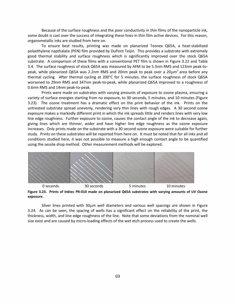
69
Because of the surface roughness and the poor conductivity in thin films of the nanoparticle ink, some doubt is cast over the success of integrating these lines in thin film active devices. For this reason, organometallic inks are studied from here on. To ensure best results, printing was made on planarized Teonex Q65A, a heat-stabilized polyethylene napthalate (PEN) film provided by DuPont Teijin. This provides a substrate with extremely good thermal stability and surface roughness which is significantly improved over the stock Q65A substrate. A comparison of these films with a conventional PET film is shown in Figure 3.22 and Table 3.4. The surface roughness of stock Q65A was measured by AFM to be 5.3nm RMS and 123nm peak-to-
peak, while planarized Q65A was 2.2nm RMS and 20nm peak to peak over a 20 m2 area before any thermal cycling. After thermal cycling at 200°C for 5 minutes, the surface roughness of stock Q65A worsened to 29nm RMS and 347nm peak-to-peak, while planarized Q65A improved to a roughness of 0.6nm RMS and 14nm peak-to-peak. Prints were made on substrates with varying amounts of exposure to ozone plasma, ensuring a variety of surface energies starting from no exposure, to 30 seconds, 5 minutes, and 10 minutes (Figure 3.23). The ozone treatment has a dramatic effect on the print behavior of the ink. Prints on the untreated substrate spread unevenly, rendering very thin lines with rough edges. A 30 second ozone exposure makes a markedly different print in which the ink spreads little and renders lines with very low line edge roughness. Further exposure to ozone, causes the contact angle of the ink to decrease again, giving lines which are thinner, wider and have higher line edge roughness as the ozone exposure increases. Only prints made on the substrate with a 30 second ozone exposure were suitable for further study. Prints on these substrates will be reported from here on. It must be noted that for all inks and all conditions studied here, it was not possible to measure a high enough contact angle to be quantified using the sessile drop method. Other measurement methods will be explored.
Figure 3.23. Prints of Inktec PR-010 made on planarized Q65A substrates with varying amounts of UV Ozone exposure.
Silver lines printed with 30 m well diameters and various well spacings are shown in Figure 3.24. As can be seen, the spacing of wells has a significant effect on the reliability of the print, the thickness, width, and line edge roughness of the line. Note that some deviations from the nominal well size exist and are caused by micro-loading effects of the wet etch process used to create the wells.
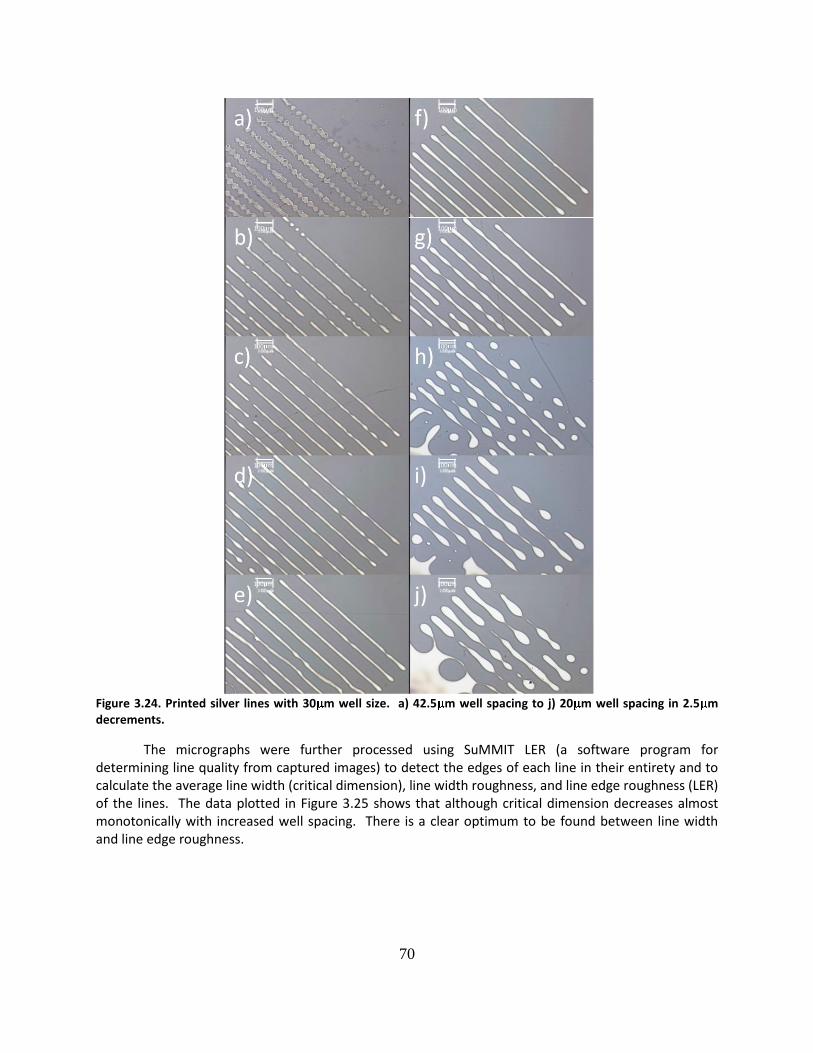
70
Figure 3.24. Printed silver lines with 30 m well size. a) 42.5 m well spacing to j) 20 m well spacing in 2.5 m decrements.
The micrographs were further processed using SuMMIT LER (a software program for determining line quality from captured images) to detect the edges of each line in their entirety and to calculate the average line width (critical dimension), line width roughness, and line edge roughness (LER) of the lines. The data plotted in Figure 3.25 shows that although critical dimension decreases almost monotonically with increased well spacing. There is a clear optimum to be found between line width and line edge roughness.
100 m
100 m
100 m
100 m
100 m
100 m
100 m
100 m
100 m
100 m
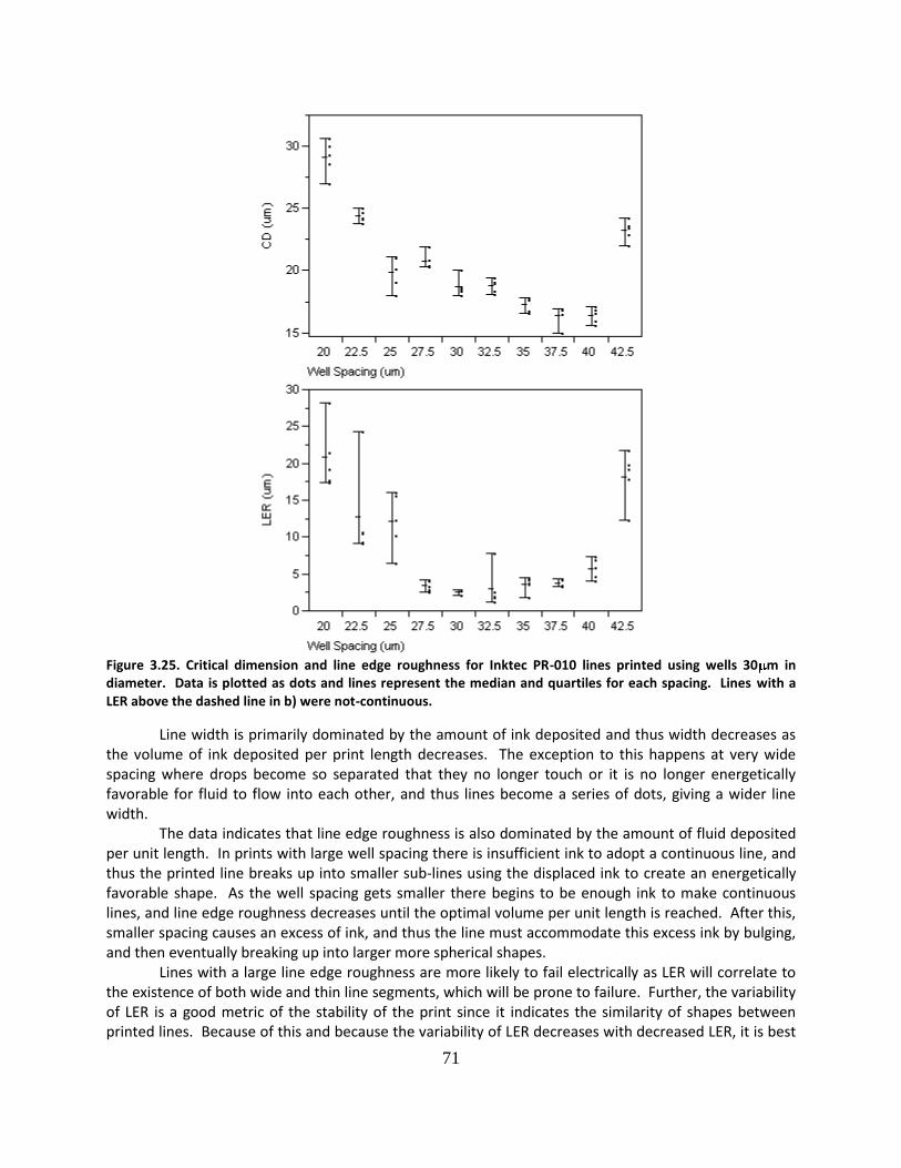
71
Figure 3.25. Critical dimension and line edge roughness for Inktec PR-010 lines printed using wells 30 m in diameter. Data is plotted as dots and lines represent the median and quartiles for each spacing. Lines with a LER above the dashed line in b) were not-continuous.
Line width is primarily dominated by the amount of ink deposited and thus width decreases as the volume of ink deposited per print length decreases. The exception to this happens at very wide spacing where drops become so separated that they no longer touch or it is no longer energetically favorable for fluid to flow into each other, and thus lines become a series of dots, giving a wider line width. The data indicates that line edge roughness is also dominated by the amount of fluid deposited per unit length. In prints with large well spacing there is insufficient ink to adopt a continuous line, and thus the printed line breaks up into smaller sub-lines using the displaced ink to create an energetically favorable shape. As the well spacing gets smaller there begins to be enough ink to make continuous lines, and line edge roughness decreases until the optimal volume per unit length is reached. After this, smaller spacing causes an excess of ink, and thus the line must accommodate this excess ink by bulging, and then eventually breaking up into larger more spherical shapes. Lines with a large line edge roughness are more likely to fail electrically as LER will correlate to the existence of both wide and thin line segments, which will be prone to failure. Further, the variability of LER is a good metric of the stability of the print since it indicates the similarity of shapes between printed lines. Because of this and because the variability of LER decreases with decreased LER, it is best
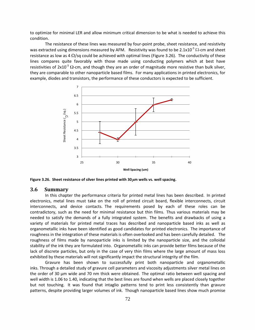
72
to optimize for minimal LER and allow minimum critical dimension to be what is needed to achieve this condition. The resistance of these lines was measured by four-point probe, sheet resistance, and resistivity
was extracted using dimensions measured by AFM. Resistivity was found to be 2.1x10⁻⁵ -cm and sheet
resistance as low as 4 /sq could be achieved with optimal lines (Figure 3.26). The conductivity of these lines compares quite favorably with those made using conducting polymers which at best have
resistivities of 2x10⁻³ -cm, and though they are an order of magnitude more resistive than bulk silver, they are comparable to other nanoparticle based films. For many applications in printed electronics, for example, diodes and transistors, the performance of these conductors is expected to be sufficient.
Figure 3.26. Sheet resistance of silver lines printed with 30 m wells vs. well spacing.
3.6 Summary In this chapter the performance criteria for printed metal lines has been described. In printed electronics, metal lines must take on the roll of printed circuit board, flexible interconnects, circuit interconnects, and device contacts. The requirements posed by each of these roles can be contradictory, such as the need for minimal resistance but thin films. Thus various materials may be needed to satisfy the demands of a fully integrated system. The benefits and drawbacks of using a variety of materials for printed metal traces has described and nanoparticle based inks as well as organometallic inks have been identified as good candidates for printed electronics. The importance of roughness in the integration of these materials is often overlooked and has been carefully detailed. The roughness of films made by nanoparticle inks is limited by the nanoparticle size, and the colloidal stability of the ink they are formulated into. Organometallic inks can provide better films because of the lack of discrete particles, but only in the case of very thin films where the large amount of mass loss exhibited by these materials will not significantly impact the structural integrity of the film. Gravure has been shown to successfully print both nanoparticle and organometallic inks. Through a detailed study of gravure cell parameters and viscosity adjustments silver metal lines on the order of 30 μm wide and 70 nm thick were obtained. The optimal ratio between well spacing and well width is 1.06 to 1.40, indicating that the best lines are found when wells are placed closely together but not touching. It was found that intaglio patterns tend to print less consistently than gravure patterns, despite providing larger volumes of ink. Though nanoparticle based lines show much promise
3
3.5
4
4.5
5
5.5
6
6.5
7
25 30 35 40
Shee
t R
esis
tan
ce (
/sq
.)
Well Spacing (um)
73
for use as interconnects and in thick film devices, their roughness must still be improved for use in thin film devices. Organometallic silver inks were shown to be capable of filling the need for a low roughness film and gravure printed lines with widths of 19 μm, line edge roughness of less than 2 μm, a 70 nm thickness a total roughness of less than 20 nm peak-to-peak, and 5 nm RMS roughness were demonstrated. These lines represent the state of the art in gravure printed electronics and have surpassed those made with currently available ink-jet printers. All together the work in this chapter is a clear demonstration of the viability of gravure as an industrial printing process for printed electronics.
3.7 Works Cited [1] Coombs, Clyde F., Printed Circuits Handbook 6th Ed. New York : McGraw-Hill, 2008. 978-07-146734-6. [2] Plummer, James D., Deal, Michael D. and Griffin, Petter B., Silicon VLSI Technology - Fundamentals, Practice, and Modeling. s.l. : Prentice Hall, 2000. [3] Wilson, S.R., Tracy, C.J. and Freeman, J.L., Jr., Handbook of Multilevel Metallization for Integrated Circuits - Materials, Technology, and Applications . s.l. : William Andrew Publishing/Noyes, 1993. [4] Suryanarayana, Cury., Mechanical Alloying and Milling. s.l. : CRC, 2004. ISBN 082474103X. [5] Heeger, Alan J., MacDiarmid, Alan G. and Shirakawa, Hideki., Nobel Prize in Chemistry. s.l. : The Royal Swedish Academy of Sciences, 2000. [6] Inzelt, György., Conducting polymers: a new era in electrochemistry. Berlin : Springer, 2008. [7] Wronski, C.R.M., "The size dependence of the meltping point of small particles of tin." s.l. : British Journal of Applied Physics, 1967, Vol. 18, pp. 1731-1737. [8] Buffat, Ph and Borel, J-P., "Size effect on the melting temperature of gold particles." s.l. : Physical Review A, 1976, Issue 6, Vol. 13, pp. 2287-2289. [9] Lewis, Laurent J., Jensen, Pablo and Barrat, Jean-Louis., "Melting, freezing, and coalescence of gold nanoclusters." s.l. : Physical Review B, 1997, Issue 4, Vol. 56, pp. 2248 - 2257. [10] Huang, Daniel C., "Plastic-compatible low-resistance printable gold nanoparticle conductors for flexible electronics." s.l. : Journal of the electrochemical society, 2003, Vol. 150, pp. 412-417. [11] S.E. Molesa, V. Subramanian, IEDM Tech. Dig., (2005) 109 - 112., [12] Kim, Dongjo, Jeong, Sunho and Moon, Jooho., "Synthesis of silver nanoparticles using the Synthesis of silver nanoparticles using thepolyol process and the influence of precursor injection." s.l. : Nanotechnology, 2006, Vol. 17, pp. 4019-4024. [13] Teng, K.F. and Vest, Robert W., "Liquid Ink Jet Printing with MOD Inks for Hybrid Microcircuits." s.l. : IEEE TRANSACTIONSO N COMPONENTSH, YBRIDS,A ND MANUFACTURINGT ECHNOLOG, 1987, Issue 4, Vol. 12, pp. 545-549. [14] Yamamoto, Osamn and Co., Matsushita Electric Industrial., Intaglio Printing Process and Its Application. 5,201,268 United States, April 12, 1991. Patent. [15] Yamamoto, Osamu and Co., Matsushita Electric Industrial., Method for producing a transparent conductive film provided with supplementary metal lines. 5,312,643 United States, May 17, 1991. Patent. [16] Sceisi, G.B., Notaro, J. and Arnone, C., "Laser Direct Writing of Gold Conductors from Metallorganic Inks." s.l. : Advanced Materials for Optics and Electronics, 1993, Vol. 2, pp. 93-98. [17] Wu, Yiliang, Li, Yuning and Ong, Ben S., "A Simple and Efficient Approach to a Printable Silver Conductor for Printed Electronics." s.l. : Jounral of the American Chemical Society, 2007, Vol. 129, pp. 1862-1863. [18] Wu, Yialiang, Li, Yuning and Ong, Ben S., "Printed Silver Ohmic Contacts for High-Mobility Organic Thin-Film Transistors." s.l. : Journal of the American Chemical Society, 2006, Vol. 128, pp. 4202-4203. [19] Emslie, Alfred G., Bonner, Francis T. and Peck, Leslie G., "Flows of a Viscous Liquid on a Rotating Disk." s.l. : Journal of Applied Physics, 1958, Issue 5, Vol. 29, pp. 858-862.

74
[20] Meyerhofer, Dietrich., "Characteristics of resist films produced by spinning." s.l. : Journal of Applied Physics, 1978, Issue 7, Vol. 49, pp. 3393-3397. [21] Veres, Janos, et al., "Low-k Insulators as the Choice of Dielectrics in Organic Field-Effect Transistors." s.l. : Advanced Functional Materials, 2003, pp. 199-204. [22] Smith, Henry I., Bachner, Frank J. and Efremow, N., "A High-Yield Photolithographic Technique for Surface Wave Devices." s.l. : Journal of the Electrochemical Society, 1971, Issue 5, Vol. 118, pp. 821-825. [23] Lan, Je-Hsiung, et al., "Patterning of Transparent Conducting Oxide Thin Films by Wet Etching for a:Si-H TFT-LCDs." s.l. : Journal of Electronic Materials, 1996, Issue 12, Vol. 25, pp. 1806-1817. [24] Hu, Hua and Larson, Ronald G., "Marangoni Effect Reverses Coffee-Ring Depositions." s.l. : Jounral of Physical Chemistry B Letters, 2006, Vol. 110, pp. 7090-7094. [25] Kim, Dongjo, et al., "Direct writing of silver conductive patterns: Improvement of film morphology and conductance by controlling solvent compositions." s.l. : Applied Physics Letters, 2006, Vol. 89, pp. 264101-264103. [26] Perelaer, Jolke, et al., "The preferential deposition of silica micro-particles at the boundary of inkjet The preferential deposition of silica micro-particles at the boundary of inkjet." s.l. : Soft Matter, 2008, Vol. 4, pp. 1072-1078. [27] Perelaer, Jolke, et al., "One-step inkjet printing of conductive silver tracks on polymer substrates." s.l. : Nanotechnology, 2009, Vol. 20, pp. 165303-165307. [28] Milgram, A. A., "Influence of Metallic Diffusion on the Adhesion of Screen Printed Silver Films." s.l. : Metallurgical Transactions, 1970, Vol. 1, pp. 696-700. [29] M. Pudas, Prog. In Org. Coat., 54 (2005) 310-316., [30] Huelber, A.C., "Ring oscillator fabricated completely by means of mass-printing technologies." s.l. : Organic Electronics, 2007, Vol. 8, pp. 480-486. [31] Redinger, David, et al., "An Ink-Jet-Deposited Passive Component Process for RFID." s.l. : IEEE Transaction on Electron Devices, 2004, Issue 12, Vol. 51, pp. 1978-1983. [32] D. Sung, A. de la Fuente Vornbrock, V. Subramanian, Submission in progress., "Scaling and Optimization of Gravure-Printed Nanoparticle Scaling and Optimization of Gravure-Printed Nanoparticle." s.l. : IEEE Transactions on Components and Packaging Technologies, Vol. accepted. [33] Zielke, Dirk, et al., "Polymer-based organic field-effect transistors using offset printed source/drain structures." s.l. : Applied Physics Letters, 2005, Vol. 87, pp. 123508-123510. [34] S. Molesa, “Ultra-Low-Cost Printed Electronics,” Ph.D. dissertation, University of California, Berkeley, 2006 [35] S. E. Fritz, “Structure and Transport in Organic Semiconductor Thin Films,” Ph.D. dissertation, University of Minnesota, Minneapolis, 2006 [36] Sung, D., "Gravure as an Industrially Viable Process for Printed Electronics." s.l. : M.S. Thesis, University of California, Berkeley, 2007. [37] Kapur, N., "A parametric study of direct gravure coating." s.l. : Chemical Engineering Science, 2003, Vol. 58, pp. 2875-2882. [38] P.C. Duiniveld, J. Fluid Mech., vol. 477 (2003) 175-200., [39] D.B. Soltman, Langmuir, vol. 24 no. 5 (2008), 2224 - 2231.
75
4 Capacitors
4.1 Capacitor structure and role in ICs Capacitors carry an extremely important role in integrated circuits. Most importantly they are a key component of every MOS transistor, and are thus ubiquitous in electronics. They are also a key element of every DRAM cell, making them prevalent in memory devices. Capacitors can also be found CCDs for digital cameras, and are commonly used as filters, integrators, and loads for tuning in analog circuitry. In large-area integrated circuits they are most commonly seen as a storage capacitor in liquid crystal displays. A capacitor is formed when any two conducting surfaces are separated by an insulator. Its simplest form would be a parallel plate capacitor where these conducting surfaces would be flat metallic plates and the insulator, could be vacuum, or any insulating material (Figure 4.1). The sole characteristic of this ideal capacitor would be its capacitance, C, which describes its ability to store charge given an applied voltage
(1) And is given by
(2)
Where A is the area of the capacitor k is the dielectric constant of the insulator 0 is the permittivity of free space, and t is the thickness of the insulator. Often the design goal is to maximize the capacitance of a capacitor so it can store maximum charge with low applied voltage. In order to do this, the area or the dielectric constant of the capacitor may be increased, and the thickness of the dielectric may be decreased. There are trade-offs in all of these approaches to maximize capacitance, and they will be described throughout the chapter.
Figure 4.1. A simple parallel plate capacitor in 2-D (left) and 3-D (right) with area A and dielectric thickness t.
Capacitors, being real devices, never operate as perfectly as they have just been described. Dielectrics do not always have constant dielectric constants and are not completely insulating, being susceptible to a variety of forms of electrical or ionic conduction, and suffer break-down under excessively high fields. Even the metal electrodes of a capacitor may not be perfect, having finite resistances, finite density of states, and can be reactive with the dielectric, leading to compositional changes at their interface as well as electromigration and dendrite formation. From the perspective of solid state physics, dielectrics are materials with large band-gaps, and negligible free carrier densities. Thus dielectrics can in theory transport carriers if they can be excited to the proper band energy in a process known as thermionic emission. With thin, nanometer scale dielectrics as are common in microelectronics, tunneling of carriers may occur through the material
76
Figure 4.2. The tunneling process may be trap assisted (Frenkel-Poole) or caused by a high electric field reducing the tunneling distance as in field emission (Fowler-Nordheim). Carrier transport in dielectrics can also occur through the motion of ionic species in the material, which can lead to slow changes in charge accumulation, or unwanted reactions with the electrode materials.
Figure 4.2. Description of three mechanisms for carrier transport through dielectrics.
The dielectric constant, or dielectric permittivity, is a measure of the electric energy a material can store in response to an electric field. This energy is stored by the polarization of the material, and thus the redistribution of charge within it. Metals being great conductors of charge can easily redistribute charge on applied field, and thus have extremely large dielectric constants. However, because they are conductive are very poor dielectrics! Insulators on the other hand must redistribute charge without releasing it from the medium. This is achieved by interfacial or space charge motion, dipolar motion, ionic motion, or electronic motion [1]. Because these processes occur at different speeds, dielectrics will exhibit different dielectric constants when electric fields are applied at different
frequencies. The effective permittivity of the material is thus modeled as frequency dependent, k( ), and it is said the material exhibits dispersion. Materials which respond to a field with interfacial or large dipolar motion, such as liquid crystals, will begin to exhibit dispersion at low frequencies, while those materials which respond by electronic motion, for example will not exhibit such decay until much higher frequencies. Thus a real material which responds to an electric field with some amount of all forms of charge motion may have a complex dispersion profile as shown below. At high fields carriers can be accelerated to the point of causing physical damage to the dielectric. This process called break-down generally causes a complete device failure and must be avoided. The maximum field a dielectric can sustain is determined by a variety of factors including the strength of the bonds between the atoms that compose the dielectric and their structural composition. However, when measuring capacitors, it is common to observe dielectric breakdown occurring below the intrinsic breakdown field, and in general three general types of failure modes can be observed when studying a population of such capacitors. Some capacitors may break down at an extremely low field, with small applied bias, indicating that the dielectric may have been already shorted or severely damaged during fabrication, this is conventionally known as Type A breakdown [2]. Some capacitors will

77
break down at fields very near their intrinsic breakdown voltage, indicating a near perfect dielectric and interface to the cathodes of the device, this is Type C breakdown. Others will break down at intermediate fields, indicating that the dielectric had some weak spots that did not immediately short, Type B breakdown. The cause of weak spots and shorting in the devices must thus be understood, and controlled to obtain reliable devices [2].
Figure 4.3. Frequency response of the dielectric constant for some material showing the cut-off frequency for each mechanism of polarization.
The breakdown process can generally be observed in two steps. First there is an increase in current injected into the dielectric. Over time, the damage caused by this injected current creates a conductive pathway through the entire dielectric. At this point the charge stored on the entire capacitor is rapidly discharged through this pathway. The discharge is usually so abrupt and powerful that it vaporizes the material around it. Observation of failed devices will thus commonly show single point defects where breakdown has occurred. Often more than one breakdown spot is seen because the vaporization process will often break the conductive path and thus “heal” the damaged site [3]. The reduction of breakdown field is caused by a wide variety of defects. In the dielectric, structural defects such as pinholes, voids, and structural inhomogeneities like grain boundaries, etc. can short the dielectric or create easy paths for electron injection. The existence of ionic or metal contamination in the dielectric can also cause reduced field resistance, as ions can move in the dielectric towards the applied field creating a nearby site for carrier injection. Roughness of the cathode material can create thin spots in the dielectric which will be subjected to higher fields, and must be minimized as discussed in Chapter 5. Contaminants on the cathode, such as dust from the environment or residual particles from processing can have the same effect, as does any roughness induced by an imperfect substrate.
4.2 Dielectrics in Printed Electronics It is evident that the choice of dielectric is of critical importance for any device. In printed electronics this choice is ever so important as the uniformity of films in terms of thickness and composition is often not as good as those in vacuum deposited processes. The purity of materials for dielectrics must be as good, if not higher as it is for semiconductor materials, and remains a challenge
1
2
3
4
5
6
7
8
9
10
1E-3 1E+0 1E+3 1E+6 1E+9 1E+12 1E+15
k (a
.u.)
Frequency (Hz)
interfacial
dipolar
ionic
electronic
78
for solution processable materials because impurities in the reactants and impurities caused by the by-products of the synthetic reactions are difficult to eliminate [4]. Further, the behavior of the dielectric as it is deposited, how it spreads, how it dries, and how it is converted to its final state must be carefully controlled: damage to any films the dielectric was deposited onto must be avoided (this could be caused by chemical reactions between materials or solvent interactions); the dielectric must be able to conformally coat the structure it was deposited onto avoiding thin spots around edges of topography; coffee ring and Marangoni effects must be minimized to maximize film thickness uniformity; and the processing temperature for the dielectric must be compatible with the rest of the process. Several types of dielectrics have been developed for printed and flexible electronics. In general these dielectrics should provide a combination of low-cost, additive processing, and low-temperature curing. They can be inorganic oxides, polymers, self-assembled monolayers, and heterogeneous organic/inorganic mixtures. Clearly the most successful inorganic oxide is silicon dioxide, which thanks to the extremely high quality films and interfaces it forms with silicon, has enabled the entire microelectronics industry. In printed electronics, silicon dioxide remains the de-facto dielectric for materials and device studies using a non-printed test structure. Since silicon dioxide is best grown by thermal oxidation of silicon, it thus remains utilized only as a dielectric material when test devices are built on silicon wafers. Thin film transistors based on hydrogenated amorphous silicon (a-Si:H), have also made extensive use of SiO2 as a dielectric having it deposited via atmospheric pressure CVD. However, better films of amorphous silicon nitride (SiNx or SiN:H) can be deposited at lower temperatures (300-350degC) with lower interface states and better stability to the high levels of hydrogen in a-Si:H [5]. Yet neither of these processes has been very successful at plastic compatible temperatures (150degC) and being subtractive processes are less suited to printed processes. Inorganic dielectrics created by the anodization of metal thin films have been extensively studied and show some promise for printed electronics. The most notable are films of tantalum oxide (k=23) [6], titanium oxide (k=80) [7], and aluminum oxide (k=9)[8] [1]. The films deposited can be thin, and thanks to their high k can give devices with a high capacitance. The anodization process occurs at room temperature in a weak citric acid solution, making anodization plastic compatible. A drawback to this approach is that an additive, printable process for the deposition of the starting metals (tantalum, titanium, and aluminum) does not exist. Further, the anodization requires a current to be passed through the film being anodized. This would make circuit design difficult as conductive pathways must be created for all anodized regions, then broken to allow the circuit to function. Finally, high-k materials have been shown to provide low mobility organic field effect transistors because the large dipoles in the material generate disorder in the electronic states near the semiconductor/insulator interface, scattering the carriers [9]. The work by Klauk and Zschieschang proposed two possible solutions to the above problems [10]. Here an aluminum gate is oxidized with a treatment of oxygen plasma creating a very thin <1nm layer of aluminum oxide. This thin film is then passivated with a self assembled monolayer dielectric which increases the dielectric thickness by another 2.5nm. The two-layer dielectric provides a very low
leakage current of 10-11 A/cm2 at low bias, only 1 A/cm2 leakage at 10 MV/cm field, and a breakdown field of 17 MV/cm. This performance is impressive and comparable if not better than thermally grown SiO2. The oxidation of the aluminum film avoids any necessity to provide current for anodization while the SAM provides an ideal surface onto which organic semiconductors can be applied. Indeed, high performance TFTs were made using this dielectric, providing a mobility of 0.4 cm2/V-s, with an on/off ratio of greater than 106, and most notably, a subthreshold swing of 100mV/dec. Yet, to make this process fully printable a good source for a printed aluminum gate must be found. Finally a major hindrance to this approach is that the dielectric cannot be grown much thicker than a few nanometers
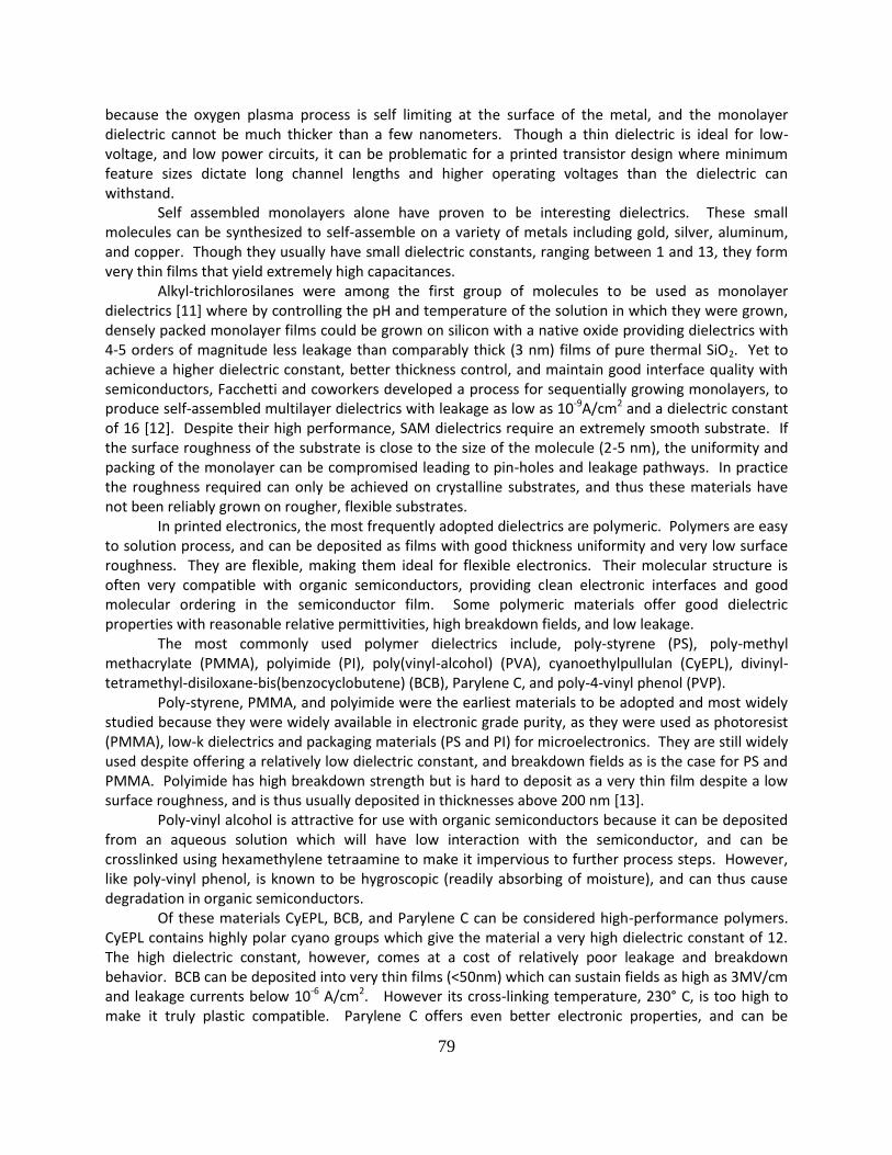
79
because the oxygen plasma process is self limiting at the surface of the metal, and the monolayer dielectric cannot be much thicker than a few nanometers. Though a thin dielectric is ideal for low-voltage, and low power circuits, it can be problematic for a printed transistor design where minimum feature sizes dictate long channel lengths and higher operating voltages than the dielectric can withstand. Self assembled monolayers alone have proven to be interesting dielectrics. These small molecules can be synthesized to self-assemble on a variety of metals including gold, silver, aluminum, and copper. Though they usually have small dielectric constants, ranging between 1 and 13, they form very thin films that yield extremely high capacitances. Alkyl-trichlorosilanes were among the first group of molecules to be used as monolayer dielectrics [11] where by controlling the pH and temperature of the solution in which they were grown, densely packed monolayer films could be grown on silicon with a native oxide providing dielectrics with 4-5 orders of magnitude less leakage than comparably thick (3 nm) films of pure thermal SiO2. Yet to achieve a higher dielectric constant, better thickness control, and maintain good interface quality with semiconductors, Facchetti and coworkers developed a process for sequentially growing monolayers, to produce self-assembled multilayer dielectrics with leakage as low as 10-9A/cm2 and a dielectric constant of 16 [12]. Despite their high performance, SAM dielectrics require an extremely smooth substrate. If the surface roughness of the substrate is close to the size of the molecule (2-5 nm), the uniformity and packing of the monolayer can be compromised leading to pin-holes and leakage pathways. In practice the roughness required can only be achieved on crystalline substrates, and thus these materials have not been reliably grown on rougher, flexible substrates. In printed electronics, the most frequently adopted dielectrics are polymeric. Polymers are easy to solution process, and can be deposited as films with good thickness uniformity and very low surface roughness. They are flexible, making them ideal for flexible electronics. Their molecular structure is often very compatible with organic semiconductors, providing clean electronic interfaces and good molecular ordering in the semiconductor film. Some polymeric materials offer good dielectric properties with reasonable relative permittivities, high breakdown fields, and low leakage. The most commonly used polymer dielectrics include, poly-styrene (PS), poly-methyl methacrylate (PMMA), polyimide (PI), poly(vinyl-alcohol) (PVA), cyanoethylpullulan (CyEPL), divinyl-tetramethyl-disiloxane-bis(benzocyclobutene) (BCB), Parylene C, and poly-4-vinyl phenol (PVP). Poly-styrene, PMMA, and polyimide were the earliest materials to be adopted and most widely studied because they were widely available in electronic grade purity, as they were used as photoresist (PMMA), low-k dielectrics and packaging materials (PS and PI) for microelectronics. They are still widely used despite offering a relatively low dielectric constant, and breakdown fields as is the case for PS and PMMA. Polyimide has high breakdown strength but is hard to deposit as a very thin film despite a low surface roughness, and is thus usually deposited in thicknesses above 200 nm [13]. Poly-vinyl alcohol is attractive for use with organic semiconductors because it can be deposited from an aqueous solution which will have low interaction with the semiconductor, and can be crosslinked using hexamethylene tetraamine to make it impervious to further process steps. However, like poly-vinyl phenol, is known to be hygroscopic (readily absorbing of moisture), and can thus cause degradation in organic semiconductors. Of these materials CyEPL, BCB, and Parylene C can be considered high-performance polymers. CyEPL contains highly polar cyano groups which give the material a very high dielectric constant of 12. The high dielectric constant, however, comes at a cost of relatively poor leakage and breakdown behavior. BCB can be deposited into very thin films (<50nm) which can sustain fields as high as 3MV/cm and leakage currents below 10-6 A/cm2. However its cross-linking temperature, 230° C, is too high to make it truly plastic compatible. Parylene C offers even better electronic properties, and can be
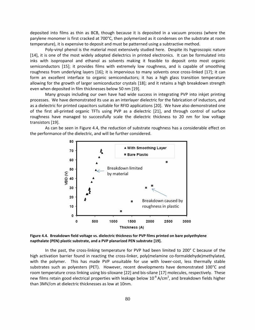
80
deposited into films as thin as BCB, though because it is deposited in a vacuum process (where the parylene monomer is first cracked at 700°C, then polymerized as it condenses on the substrate at room temperature), it is expensive to deposit and must be patterned using a subtractive method. Poly-vinyl phenol is the material most extensively studied here. Despite its hygroscopic nature [14], it is one of the most widely adopted dielectrics in printed electronics. It can be formulated into inks with isopropanol and ethanol as solvents making it feasible to deposit onto most organic semiconductors [15]; it provides films with extremely low roughness, and is capable of smoothing roughness from underlying layers [16]; it is impervious to many solvents once cross-linked [17]; it can form an excellent interface to organic semiconductors; it has a high glass transition temperature allowing for the growth of larger semiconductor crystals [18]; and it retains a high breakdown strength even when deposited in film thicknesses below 50 nm [19]. Many groups including our own have had wide success in integrating PVP into inkjet printing processes. We have demonstrated its use as an interlayer dielectric for the fabrication of inductors, and as a dielectric for printed capacitors suitable for RFID applications [20]. We have also demonstrated one of the first all-printed organic TFTs using PVP as a dielectric [21], and through control of surface roughness have managed to successfully scale the dielectric thickness to 20 nm for low voltage transistors [19]. As can be seen in Figure 4.4, the reduction of substrate roughness has a considerable effect on the performance of the dielectric, and will be further considered.
Figure 4.4. Breakdown field voltage vs. dielectric thickness for PVP films printed on bare polyethylene napthalate (PEN) plastic substrate, and a PVP planarized PEN substrate [19].
In the past, the cross-linking temperature for PVP had been limited to 200° C because of the high activation barrier found in reacting the cross-linker, poly(melamine co-formaldehyde)methylated, with the polymer. This has made PVP unsuitable for use with lower-cost, less thermally stable substrates such as polyesters (PET). However, recent developments have demonstrated 100°C and room temperature cross linking using bis-siloxane [22] and bis-silane [17] molecules, respectively. These new films retain good electrical properties with leakage below 10-8 A/cm2, and breakdown fields higher than 3MV/cm at dielectric thicknesses as low at 10nm.
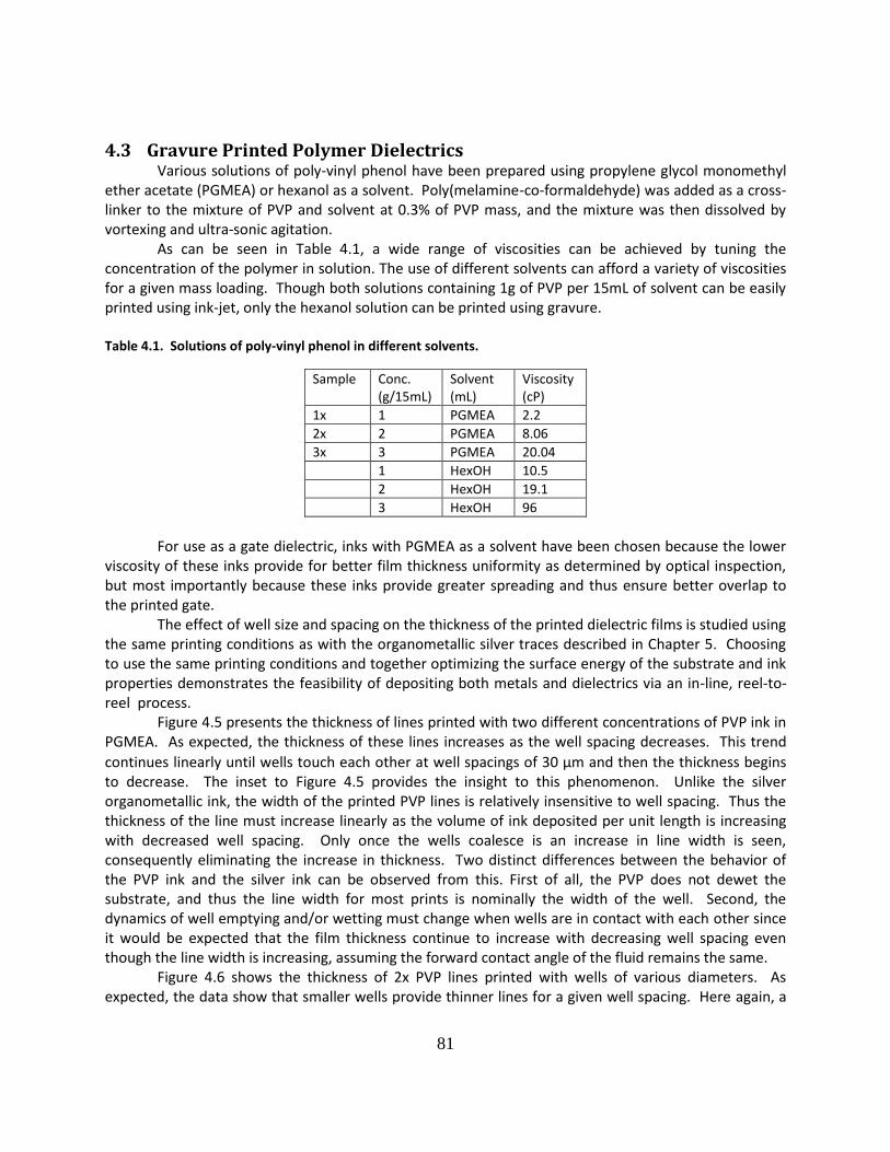
81
4.3 Gravure Printed Polymer Dielectrics Various solutions of poly-vinyl phenol have been prepared using propylene glycol monomethyl ether acetate (PGMEA) or hexanol as a solvent. Poly(melamine-co-formaldehyde) was added as a cross-linker to the mixture of PVP and solvent at 0.3% of PVP mass, and the mixture was then dissolved by vortexing and ultra-sonic agitation. As can be seen in Table 4.1, a wide range of viscosities can be achieved by tuning the concentration of the polymer in solution. The use of different solvents can afford a variety of viscosities for a given mass loading. Though both solutions containing 1g of PVP per 15mL of solvent can be easily printed using ink-jet, only the hexanol solution can be printed using gravure. Table 4.1. Solutions of poly-vinyl phenol in different solvents.
Sample Conc. (g/15mL)
Solvent (mL)
Viscosity (cP)
1x 1 PGMEA 2.2
2x 2 PGMEA 8.06
3x 3 PGMEA 20.04
1 HexOH 10.5
2 HexOH 19.1
3 HexOH 96
For use as a gate dielectric, inks with PGMEA as a solvent have been chosen because the lower viscosity of these inks provide for better film thickness uniformity as determined by optical inspection, but most importantly because these inks provide greater spreading and thus ensure better overlap to the printed gate. The effect of well size and spacing on the thickness of the printed dielectric films is studied using the same printing conditions as with the organometallic silver traces described in Chapter 5. Choosing to use the same printing conditions and together optimizing the surface energy of the substrate and ink properties demonstrates the feasibility of depositing both metals and dielectrics via an in-line, reel-to-reel process. Figure 4.5 presents the thickness of lines printed with two different concentrations of PVP ink in PGMEA. As expected, the thickness of these lines increases as the well spacing decreases. This trend
continues linearly until wells touch each other at well spacings of 30 μm and then the thickness begins to decrease. The inset to Figure 4.5 provides the insight to this phenomenon. Unlike the silver organometallic ink, the width of the printed PVP lines is relatively insensitive to well spacing. Thus the thickness of the line must increase linearly as the volume of ink deposited per unit length is increasing with decreased well spacing. Only once the wells coalesce is an increase in line width is seen, consequently eliminating the increase in thickness. Two distinct differences between the behavior of the PVP ink and the silver ink can be observed from this. First of all, the PVP does not dewet the substrate, and thus the line width for most prints is nominally the width of the well. Second, the dynamics of well emptying and/or wetting must change when wells are in contact with each other since it would be expected that the film thickness continue to increase with decreasing well spacing even though the line width is increasing, assuming the forward contact angle of the fluid remains the same. Figure 4.6 shows the thickness of 2x PVP lines printed with wells of various diameters. As expected, the data show that smaller wells provide thinner lines for a given well spacing. Here again, a
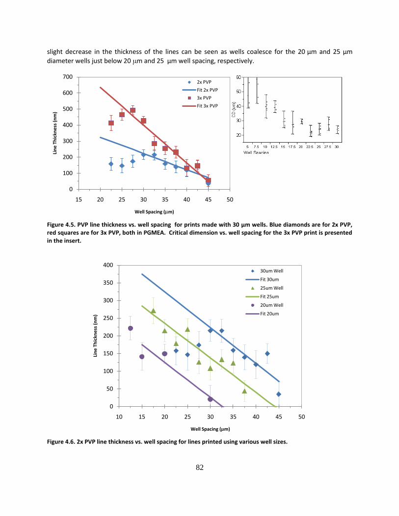
82
slight decrease in the thickness of the lines can be seen as wells coalesce for the 20 μm and 25 μm
diameter wells just below 20 m and 25 μm well spacing, respectively.
Figure 4.5. PVP line thickness vs. well spacing for prints made with 30 μm wells. Blue diamonds are for 2x PVP, red squares are for 3x PVP, both in PGMEA. Critical dimension vs. well spacing for the 3x PVP print is presented in the insert.
Figure 4.6. 2x PVP line thickness vs. well spacing for lines printed using various well sizes.
0
100
200
300
400
500
600
700
15 20 25 30 35 40 45 50
Lin
e T
hic
kne
ss (
nm
)
Well Spacing ( m)
2x PVP
Fit 2x PVP
3x PVP
Fit 3x PVP
0
50
100
150
200
250
300
350
400
10 15 20 25 30 35 40 45 50
Lin
e T
hic
kne
ss (
nm
)
Well Spacing ( m)
30um Well
Fit 30um
25um Well
Fit 25um
20um Well
Fit 20um
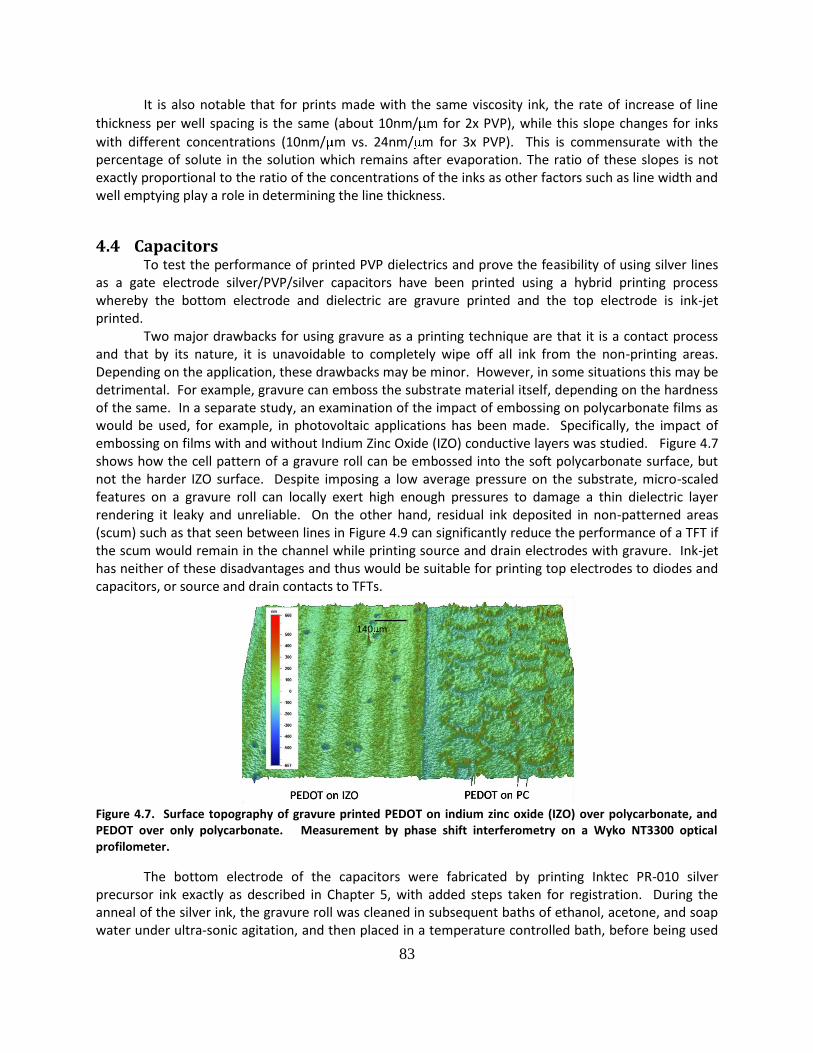
83
It is also notable that for prints made with the same viscosity ink, the rate of increase of line
thickness per well spacing is the same (about 10nm/ m for 2x PVP), while this slope changes for inks
with different concentrations (10nm/ m vs. 24nm/ m for 3x PVP). This is commensurate with the percentage of solute in the solution which remains after evaporation. The ratio of these slopes is not exactly proportional to the ratio of the concentrations of the inks as other factors such as line width and well emptying play a role in determining the line thickness.
4.4 Capacitors To test the performance of printed PVP dielectrics and prove the feasibility of using silver lines as a gate electrode silver/PVP/silver capacitors have been printed using a hybrid printing process whereby the bottom electrode and dielectric are gravure printed and the top electrode is ink-jet printed. Two major drawbacks for using gravure as a printing technique are that it is a contact process and that by its nature, it is unavoidable to completely wipe off all ink from the non-printing areas. Depending on the application, these drawbacks may be minor. However, in some situations this may be detrimental. For example, gravure can emboss the substrate material itself, depending on the hardness of the same. In a separate study, an examination of the impact of embossing on polycarbonate films as would be used, for example, in photovoltaic applications has been made. Specifically, the impact of embossing on films with and without Indium Zinc Oxide (IZO) conductive layers was studied. Figure 4.7 shows how the cell pattern of a gravure roll can be embossed into the soft polycarbonate surface, but not the harder IZO surface. Despite imposing a low average pressure on the substrate, micro-scaled features on a gravure roll can locally exert high enough pressures to damage a thin dielectric layer rendering it leaky and unreliable. On the other hand, residual ink deposited in non-patterned areas (scum) such as that seen between lines in Figure 4.9 can significantly reduce the performance of a TFT if the scum would remain in the channel while printing source and drain electrodes with gravure. Ink-jet has neither of these disadvantages and thus would be suitable for printing top electrodes to diodes and capacitors, or source and drain contacts to TFTs.
Figure 4.7. Surface topography of gravure printed PEDOT on indium zinc oxide (IZO) over polycarbonate, and PEDOT over only polycarbonate. Measurement by phase shift interferometry on a Wyko NT3300 optical profilometer.
The bottom electrode of the capacitors were fabricated by printing Inktec PR-010 silver precursor ink exactly as described in Chapter 5, with added steps taken for registration. During the anneal of the silver ink, the gravure roll was cleaned in subsequent baths of ethanol, acetone, and soap water under ultra-sonic agitation, and then placed in a temperature controlled bath, before being used
140 m

84
to print the following layer. After converting and annealing the silver ink, the substrate was re-mounted and aligned to the gravure roll, which was removed from its bath and rinsed with DI water, acetone, and isopropanol, then dried in N2. 2x PVP was chosen as a test ink because it provided film thicknesses which were close to those commonly seen in printed TFT (100nm-300nm). The PVP ink was printed using the same printing conditions as before and then annealed for 15 minutes at 150° C in a vacuum oven, then at 200° C for 5 minutes on a hot plate to fully crosslink the dielectric. Finally the top contact was printed using a Dimatix DMP ink-jet printer and Cabot CCI-300 silver nanoparticle ink optimized to print on PVP. The wetting behavior of the PVP was found to be considerably different above a silver patterned substrate from that described in section 4.3. As can be seen in Figure 4.8 the PVP preferentially wet the
silver lines over the substrate even with misalignment of 77 m (only a small contact between PVP and silver is required). The dielectric in this case was considerably thicker than expected, ranging between
190nm and 310nm for lines printed with 30 m wells and the capacitors yielded relatively low breakdown fields considering their thickness (Figure 4.11). This is likely due to thinning of the dielectric at the edges of the metal line.
Figure 4.8. Poly-vinyl phenol printed on top of Inktec PR-010 silver. PVP preferentially wets the silver ink despite the poor registration of this print.
Figure 4.9. Capacitors printed using a hybrid gravure / ink-jet printing process. Bottom electrodes and dielectric are printed using 30 μm diameter gravure wells with 30 μm spacing, the top electrode is printed using ink-jet.
To ensure proper full overlap of the metal line by the dielectric an additional ozone treatment was added to the process. In this case the sample was placed under UV-ozone for 5 minutes after the silver patterned substrate was annealed, and immediately before the PVP was printed. This improved wetting significantly allowing PVP lines fully coat the metallic traces as seen in Figure 4.9. In this case, PVP lines spread significantly more than when treated with 30 seconds of UV-ozone (as above) yielding
100 m
100 m
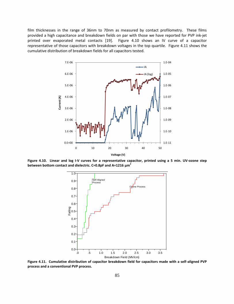
85
film thicknesses in the range of 36nm to 70nm as measured by contact profilometry. These films provided a high capacitance and breakdown fields on par with those we have reported for PVP ink-jet printed over evaporated metal contacts [19]. Figure 4.10 shows an IV curve of a capacitor representative of those capacitors with breakdown voltages in the top quartile. Figure 4.11 shows the cumulative distribution of breakdown fields for all capacitors tested.
Figure 4.10. Linear and log I-V curves for a representative capacitor, printed using a 5 min. UV-ozone step between bottom contact and dielectric. C=0.8pF and A=1216 μm
2
Figure 4.11. Cumulative distribution of capacitor breakdown field for capacitors made with a self-aligned PVP process and a conventional PVP process.
1.E-11
1.E-10
1.E-09
1.E-08
1.E-07
1.E-06
1.E-05
1.E-04
0.E+00
1.E-06
2.E-06
3.E-06
4.E-06
5.E-06
6.E-06
7.E-06
0 10 20 30 40 50
Cu
rre
nt
(A)
Voltage (V)
IA
IA (log)
0.0
0.1
0.2
0.3
0.4
0.5
0.6
0.7
0.8
0.9
1.0
Faili
ng
.0 .5 1.0 1.5 2.0 2.5 3.0 3.5
Breakdown Field (MV/cm)
Ozone
Self Aligned
Failure Plot
Ozone Process
Self-Aligned Process
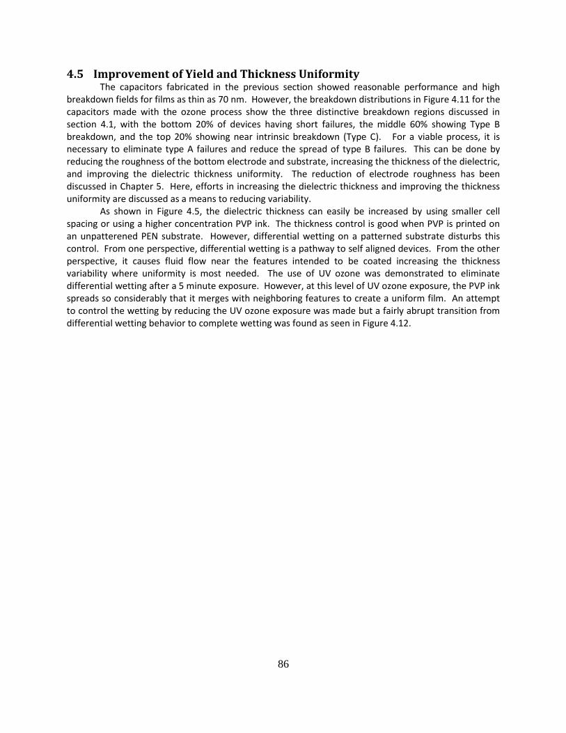
86
4.5 Improvement of Yield and Thickness Uniformity The capacitors fabricated in the previous section showed reasonable performance and high breakdown fields for films as thin as 70 nm. However, the breakdown distributions in Figure 4.11 for the capacitors made with the ozone process show the three distinctive breakdown regions discussed in section 4.1, with the bottom 20% of devices having short failures, the middle 60% showing Type B breakdown, and the top 20% showing near intrinsic breakdown (Type C). For a viable process, it is necessary to eliminate type A failures and reduce the spread of type B failures. This can be done by reducing the roughness of the bottom electrode and substrate, increasing the thickness of the dielectric, and improving the dielectric thickness uniformity. The reduction of electrode roughness has been discussed in Chapter 5. Here, efforts in increasing the dielectric thickness and improving the thickness uniformity are discussed as a means to reducing variability. As shown in Figure 4.5, the dielectric thickness can easily be increased by using smaller cell spacing or using a higher concentration PVP ink. The thickness control is good when PVP is printed on an unpatterened PEN substrate. However, differential wetting on a patterned substrate disturbs this control. From one perspective, differential wetting is a pathway to self aligned devices. From the other perspective, it causes fluid flow near the features intended to be coated increasing the thickness variability where uniformity is most needed. The use of UV ozone was demonstrated to eliminate differential wetting after a 5 minute exposure. However, at this level of UV ozone exposure, the PVP ink spreads so considerably that it merges with neighboring features to create a uniform film. An attempt to control the wetting by reducing the UV ozone exposure was made but a fairly abrupt transition from differential wetting behavior to complete wetting was found as seen in Figure 4.12.
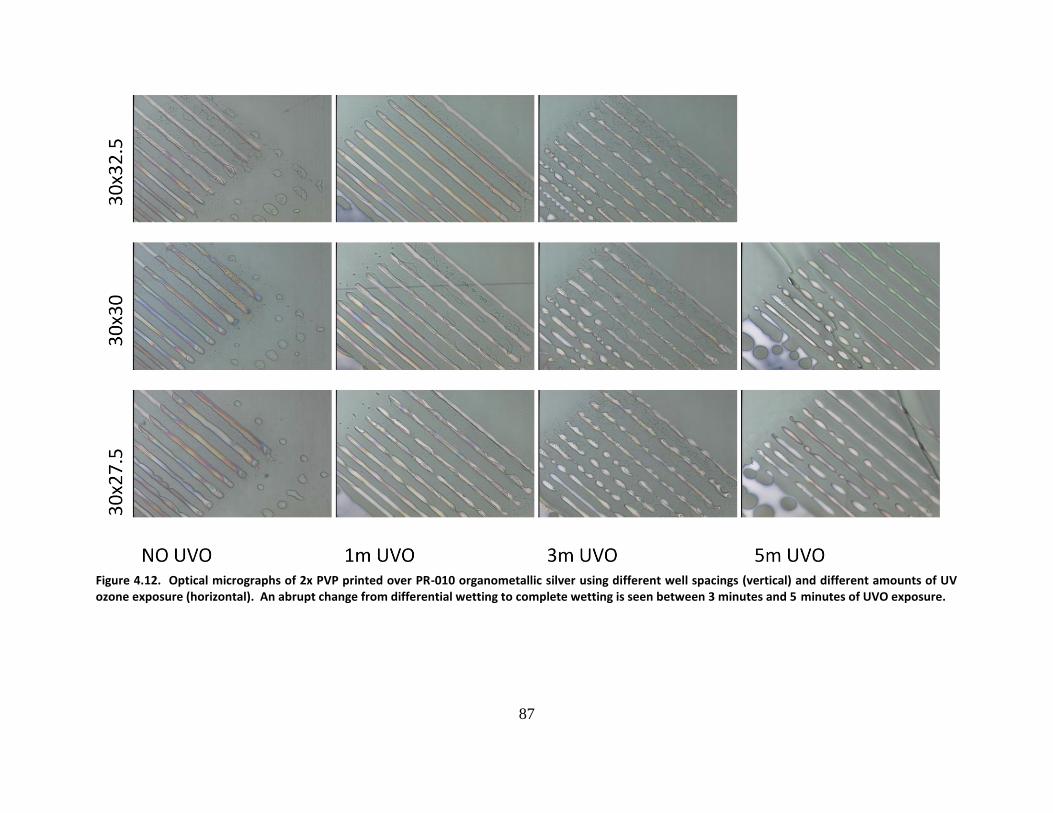
87
Figure 4.12. Optical micrographs of 2x PVP printed over PR-010 organometallic silver using different well spacings (vertical) and different amounts of UV ozone exposure (horizontal). An abrupt change from differential wetting to complete wetting is seen between 3 minutes and 5 minutes of UVO exposure.
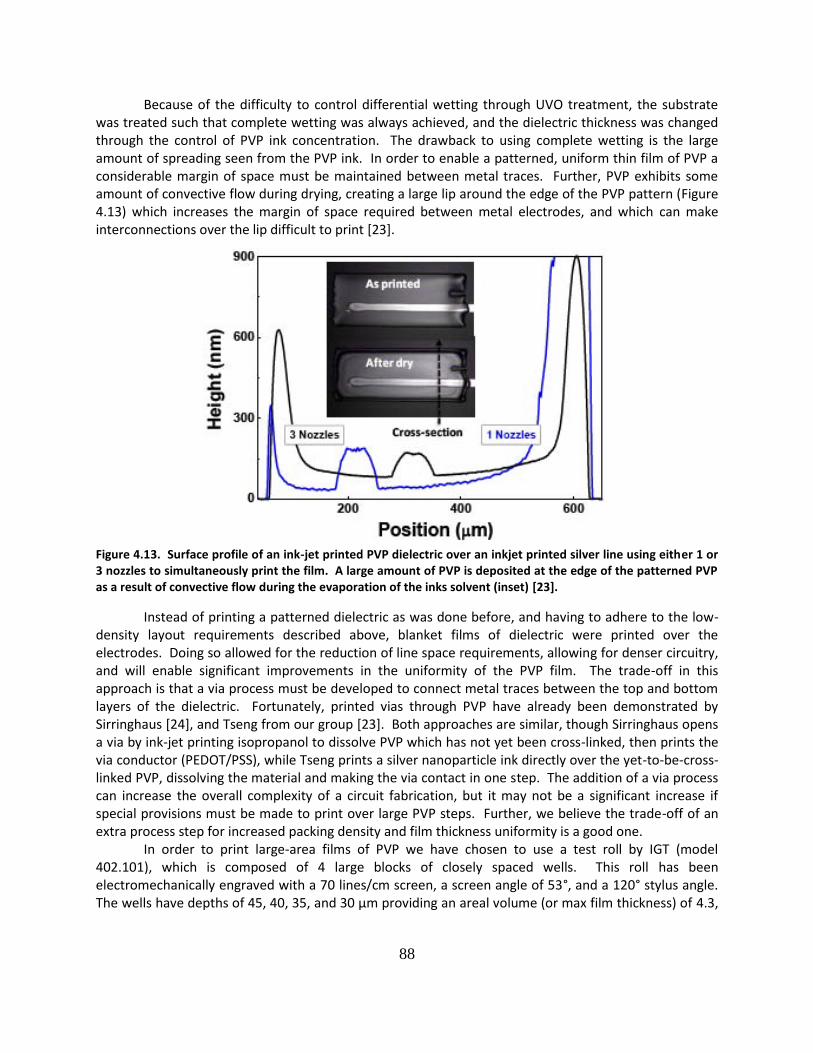
88
Because of the difficulty to control differential wetting through UVO treatment, the substrate was treated such that complete wetting was always achieved, and the dielectric thickness was changed through the control of PVP ink concentration. The drawback to using complete wetting is the large amount of spreading seen from the PVP ink. In order to enable a patterned, uniform thin film of PVP a considerable margin of space must be maintained between metal traces. Further, PVP exhibits some amount of convective flow during drying, creating a large lip around the edge of the PVP pattern (Figure 4.13) which increases the margin of space required between metal electrodes, and which can make interconnections over the lip difficult to print [23].
Figure 4.13. Surface profile of an ink-jet printed PVP dielectric over an inkjet printed silver line using either 1 or 3 nozzles to simultaneously print the film. A large amount of PVP is deposited at the edge of the patterned PVP as a result of convective flow during the evaporation of the inks solvent (inset) [23].
Instead of printing a patterned dielectric as was done before, and having to adhere to the low-density layout requirements described above, blanket films of dielectric were printed over the electrodes. Doing so allowed for the reduction of line space requirements, allowing for denser circuitry, and will enable significant improvements in the uniformity of the PVP film. The trade-off in this approach is that a via process must be developed to connect metal traces between the top and bottom layers of the dielectric. Fortunately, printed vias through PVP have already been demonstrated by Sirringhaus [24], and Tseng from our group [23]. Both approaches are similar, though Sirringhaus opens a via by ink-jet printing isopropanol to dissolve PVP which has not yet been cross-linked, then prints the via conductor (PEDOT/PSS), while Tseng prints a silver nanoparticle ink directly over the yet-to-be-cross-linked PVP, dissolving the material and making the via contact in one step. The addition of a via process can increase the overall complexity of a circuit fabrication, but it may not be a significant increase if special provisions must be made to print over large PVP steps. Further, we believe the trade-off of an extra process step for increased packing density and film thickness uniformity is a good one. In order to print large-area films of PVP we have chosen to use a test roll by IGT (model 402.101), which is composed of 4 large blocks of closely spaced wells. This roll has been electromechanically engraved with a 70 lines/cm screen, a screen angle of 53°, and a 120° stylus angle. The wells have depths of 45, 40, 35, and 30 μm providing an areal volume (or max film thickness) of 4.3,
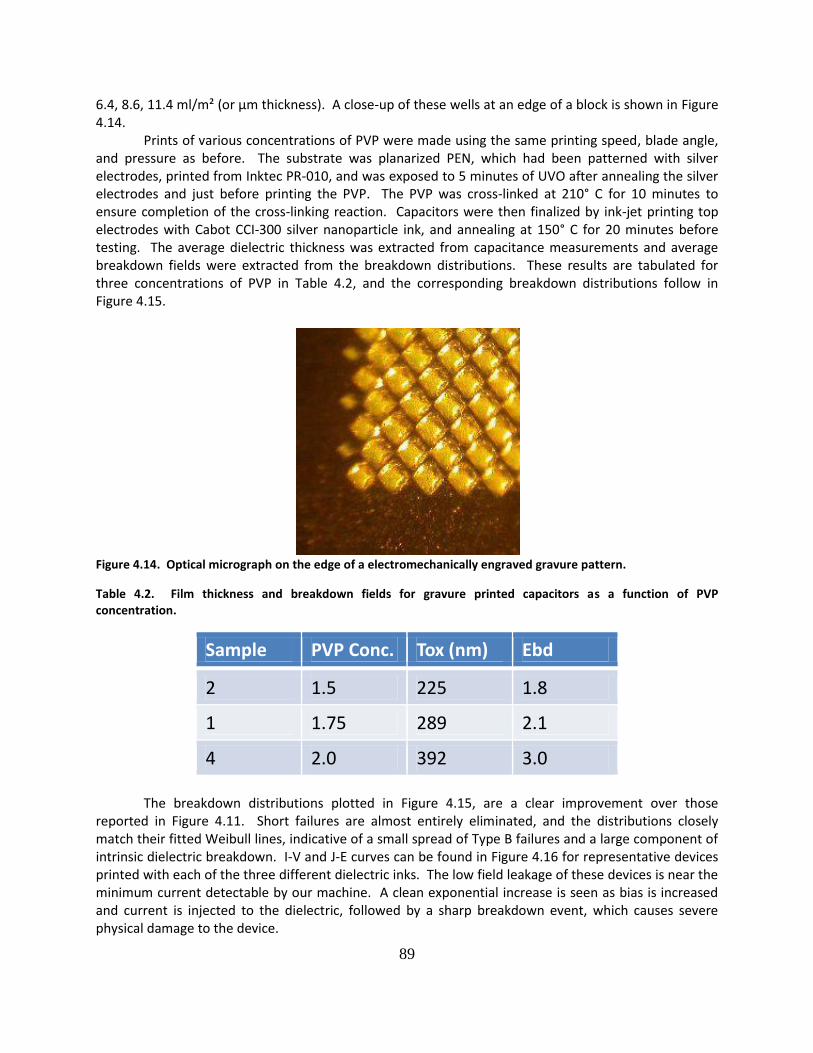
89
6.4, 8.6, 11.4 ml/m² (or μm thickness). A close-up of these wells at an edge of a block is shown in Figure 4.14. Prints of various concentrations of PVP were made using the same printing speed, blade angle, and pressure as before. The substrate was planarized PEN, which had been patterned with silver electrodes, printed from Inktec PR-010, and was exposed to 5 minutes of UVO after annealing the silver electrodes and just before printing the PVP. The PVP was cross-linked at 210° C for 10 minutes to ensure completion of the cross-linking reaction. Capacitors were then finalized by ink-jet printing top electrodes with Cabot CCI-300 silver nanoparticle ink, and annealing at 150° C for 20 minutes before testing. The average dielectric thickness was extracted from capacitance measurements and average breakdown fields were extracted from the breakdown distributions. These results are tabulated for three concentrations of PVP in Table 4.2, and the corresponding breakdown distributions follow in Figure 4.15.
Figure 4.14. Optical micrograph on the edge of a electromechanically engraved gravure pattern.
Table 4.2. Film thickness and breakdown fields for gravure printed capacitors as a function of PVP concentration.
Sample PVP Conc. Tox (nm) Ebd
2 1.5 225 1.8
1 1.75 289 2.1
4 2.0 392 3.0
The breakdown distributions plotted in Figure 4.15, are a clear improvement over those reported in Figure 4.11. Short failures are almost entirely eliminated, and the distributions closely match their fitted Weibull lines, indicative of a small spread of Type B failures and a large component of intrinsic dielectric breakdown. I-V and J-E curves can be found in Figure 4.16 for representative devices printed with each of the three different dielectric inks. The low field leakage of these devices is near the minimum current detectable by our machine. A clean exponential increase is seen as bias is increased and current is injected to the dielectric, followed by a sharp breakdown event, which causes severe physical damage to the device.
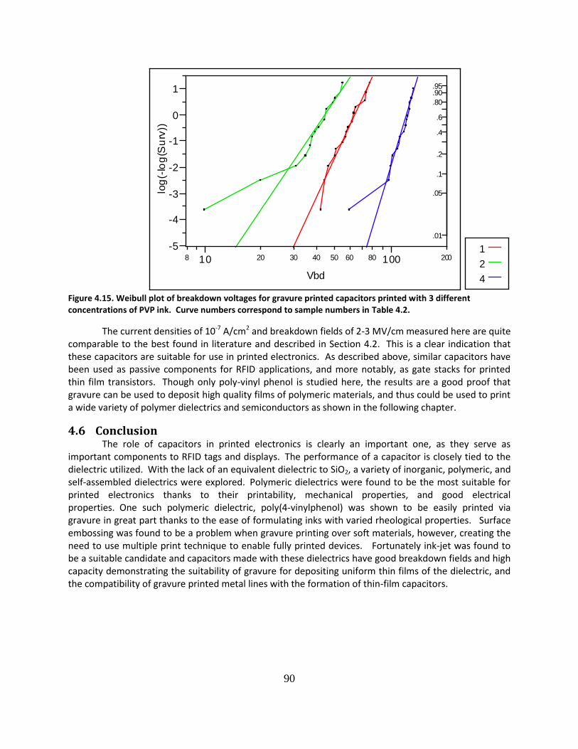
90
Figure 4.15. Weibull plot of breakdown voltages for gravure printed capacitors printed with 3 different concentrations of PVP ink. Curve numbers correspond to sample numbers in Table 4.2.
The current densities of 10-7 A/cm2 and breakdown fields of 2-3 MV/cm measured here are quite comparable to the best found in literature and described in Section 4.2. This is a clear indication that these capacitors are suitable for use in printed electronics. As described above, similar capacitors have been used as passive components for RFID applications, and more notably, as gate stacks for printed thin film transistors. Though only poly-vinyl phenol is studied here, the results are a good proof that gravure can be used to deposit high quality films of polymeric materials, and thus could be used to print a wide variety of polymer dielectrics and semiconductors as shown in the following chapter.
4.6 Conclusion The role of capacitors in printed electronics is clearly an important one, as they serve as important components to RFID tags and displays. The performance of a capacitor is closely tied to the dielectric utilized. With the lack of an equivalent dielectric to SiO2, a variety of inorganic, polymeric, and self-assembled dielectrics were explored. Polymeric dielectrics were found to be the most suitable for printed electronics thanks to their printability, mechanical properties, and good electrical properties. One such polymeric dielectric, poly(4-vinylphenol) was shown to be easily printed via gravure in great part thanks to the ease of formulating inks with varied rheological properties. Surface embossing was found to be a problem when gravure printing over soft materials, however, creating the need to use multiple print technique to enable fully printed devices. Fortunately ink-jet was found to be a suitable candidate and capacitors made with these dielectrics have good breakdown fields and high capacity demonstrating the suitability of gravure for depositing uniform thin films of the dielectric, and the compatibility of gravure printed metal lines with the formation of thin-film capacitors.
-5
-4
-3
-2
-1
0
1
log
(-lo
g(S
urv
))
.95
.90
.80
.6
.4
.2
.1
.05
.01
10 8 100 80 60 50 40 30 20 200
Vbd
1
2
4
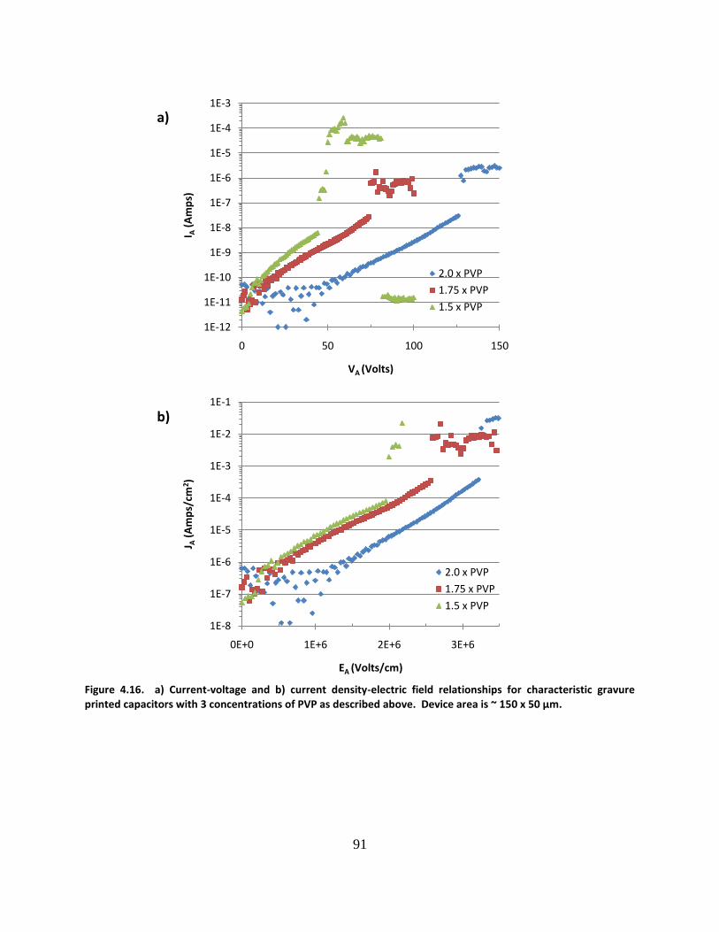
91
Figure 4.16. a) Current-voltage and b) current density-electric field relationships for characteristic gravure printed capacitors with 3 concentrations of PVP as described above. Device area is ~ 150 x 50 μm.
1E-12
1E-11
1E-10
1E-9
1E-8
1E-7
1E-6
1E-5
1E-4
1E-3
0 50 100 150
I A(A
mp
s)
VA (Volts)
2.0 x PVP
1.75 x PVP
1.5 x PVP
1E-8
1E-7
1E-6
1E-5
1E-4
1E-3
1E-2
1E-1
0E+0 1E+6 2E+6 3E+6
J A(A
mp
s/cm
2 )
EA (Volts/cm)
2.0 x PVP
1.75 x PVP
1.5 x PVP
b)
a)

92
4.7 Works Cited [1] Bao, Zhenan and Locklin, Jason., Organic Field Effect Transistors. Boca Raton : CRC Press, 2007. [2] Wolf, S., Silicon Processing for the VLSI Era Vol. 3 - The submicron MOSFET. Sunset Beach, CA : Lattice Press, 1995. [3] Solomon, P., "Breakdown in Silicon Dioxide - A Review." s.l. : Journal of Vacuum Science and Technology, 1977, Vol. 14, p. 1122. [4] McCulloch, Iain, et al., "Semiconducting Thienothiphene Copolymers: Design, Synthesis, Morphology, and Performance in Thin-Film Organic Transistors." s.l. : Advanced Materials, 2009, Vol. 21, pp. 1091-1109. [5] Kagan, Cherie R. and Andry, Paul., Thin-Film Transistors. New York : Marcel Dekker, Inc., 2003. [6] Tate, Jennifer, et al., "Anodization and Microcontact Printing on Electroless Silver: Solution-Based Fabrication Procedures for Low-Voltage Electronic Systems with Organic Active Components." s.l. : Langmuir, 2000, Vol. 16, pp. 6054-6060. [7] Majewski, Leszek Artur, Schroeder, Raoul and Grell, Martin., "One-Volt Organic Transistor." s.l. : Advanced Materials, 2005, Vol. 17, pp. 192-196. [8] Majewski, Leszek Artur, et al., "A novel gate insulator for flexible electronics." s.l. : Organic Electronics, 2003, Vol. 4, pp. 27-32. [9] Veres, Janos, et al., "Low-k Insulators as the Choice of Dielectrics in Organic Field-Effect Transistors." s.l. : Advanced Functional Materials, 2003, pp. 199-204. [10] Klauk, Hagen, et al., "Low-Voltage Flexible Organic Circuits with Molecular Gate Dielectrics." s.l. : IEEE International Electron Devices Meeting, 2004. p. 15.2.1. [11] Vuillaume, D., et al., "Organic insulating films of nanometer thickness." s.l. : Applied Physics Letters, 1996, Issue 11, Vol. 69, pp. 1646-1648. [12] Yoon, Myung-Han, Facchetti, Antonio and Marks, Tobin J., "sigma-pi molecular dielectric multilayers for low-votlage organic thin-film transistors." s.l. : Proceedings of the National Academy of Science, 2005, Issue 13, Vol. 102, pp. 4678-4682. [13] Kato, Yusaku, et al., "High mobility of pentacene field-effect transistors with polyimide gate dielectric layers." s.l. : Applied Physics Letters, 2004, Vol. 84, p. 3789. doi:10.1063/1.1739508. [14] Sandberg, H. G. O., et al., "High-Performance All-Polymer Transistor Utilizing a Hygroscopic Insulator." s.l. : Advanced Materials, 2004, Issue 13, Vol. 16, pp. 1112-1115. [15] C.J. Drury, APL, Vol. 73 No. 1, (1998) 108-110., [16] Lee, Jiyoul, et al., "Flexible semitransparent pentacene thin-film transistors with polymer dielectric layers and NiOx electrodes." s.l. : Applied Physics Letters, 2005, Vol. 87, p. 023504. doi:10.1063/1.1996839. [17] Yoon, Myung-Han, et al., "Low-Voltage Organic Field-Effect Transistors and Inverters Enabled by Ultrathin Cross-Linked Polymers as Gate Dielectrics." s.l. : Journal of the American Chemical Society, 2005, Vol. 127, pp. 10388-10395. [18] Kim, Choongik, Facchetti, Antonio and Marks, Tobin J., "Polymer Gate Dielectric Surface Viscoelasticity Modulates Pentacene Transistor Performance." s.l. : Science, 2007, Vol. 318, pp. 76-81. [19] S.E. Molesa, V. Subramanian, IEDM Tech. Dig., (2005) 109 - 112., [20] Redinger, David, et al., "An Ink-Jet-Deposited Passive Component Process for RFID." s.l. : IEEE Transaction on Electron Devices, 2004, Issue 12, Vol. 51, pp. 1978-1983. [21] Molesa, Steve E., et al., "A high-performance all-inkjetted organic transistor technology." s.l. : IEEE International Electron Devices Meeting, 2004. p. 1072. [22] Kim, Choongik, et al., "Printable Cross-Linked Polymer Blend Dielectrics. Design Strategies, Synthesis, Microstructures, and Electrical Properties, with Organic Field-Effect Transistors as Testbeds." s.l. : Journal of the American Chemical Society, 2008, Issue 21, Vol. 130, pp. 6867–6878.

93
[23] Tseng, Huai-Yuan, Yin, Shong and Subramanian, Vivek., "Optimization of inkjet-based process modules for printed transistor circuits." Louisville, Kentucky : 25th International Conference on Digital Printing Technologies: Digital Fabrication 2009, September 20-24, 2009. [24] Sirringhaus, H, et al., "High-Resolution Inkjet Printing of All-Polymer Transistor Circuits." s.l. : Science, 2000, Issue 5499, Vol. 290, pp. 2123 - 2126. DOI: 10.1126/science.290.5499.2123.
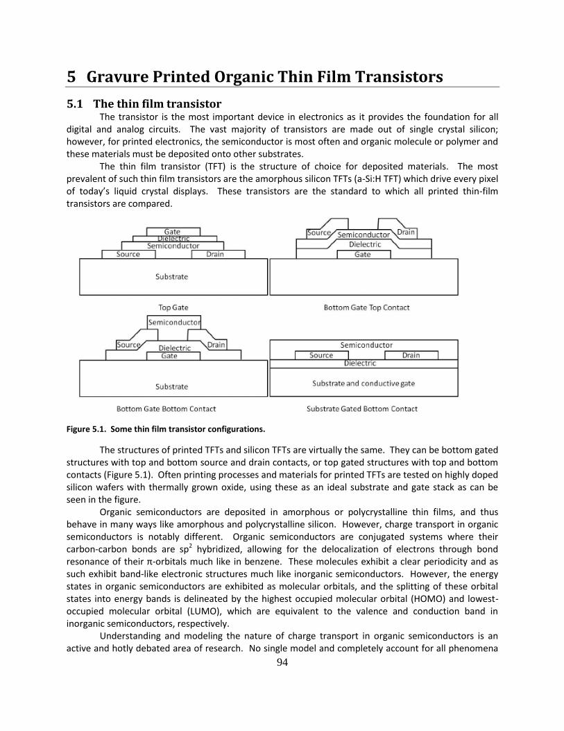
94
5 Gravure Printed Organic Thin Film Transistors
5.1 The thin film transistor The transistor is the most important device in electronics as it provides the foundation for all digital and analog circuits. The vast majority of transistors are made out of single crystal silicon; however, for printed electronics, the semiconductor is most often and organic molecule or polymer and these materials must be deposited onto other substrates. The thin film transistor (TFT) is the structure of choice for deposited materials. The most prevalent of such thin film transistors are the amorphous silicon TFTs (a-Si:H TFT) which drive every pixel of today’s liquid crystal displays. These transistors are the standard to which all printed thin-film transistors are compared.
Figure 5.1. Some thin film transistor configurations.
The structures of printed TFTs and silicon TFTs are virtually the same. They can be bottom gated structures with top and bottom source and drain contacts, or top gated structures with top and bottom contacts (Figure 5.1). Often printing processes and materials for printed TFTs are tested on highly doped silicon wafers with thermally grown oxide, using these as an ideal substrate and gate stack as can be seen in the figure. Organic semiconductors are deposited in amorphous or polycrystalline thin films, and thus behave in many ways like amorphous and polycrystalline silicon. However, charge transport in organic semiconductors is notably different. Organic semiconductors are conjugated systems where their carbon-carbon bonds are sp2 hybridized, allowing for the delocalization of electrons through bond resonance of their π-orbitals much like in benzene. These molecules exhibit a clear periodicity and as such exhibit band-like electronic structures much like inorganic semiconductors. However, the energy states in organic semiconductors are exhibited as molecular orbitals, and the splitting of these orbital states into energy bands is delineated by the highest occupied molecular orbital (HOMO) and lowest-occupied molecular orbital (LUMO), which are equivalent to the valence and conduction band in inorganic semiconductors, respectively. Understanding and modeling the nature of charge transport in organic semiconductors is an active and hotly debated area of research. No single model and completely account for all phenomena
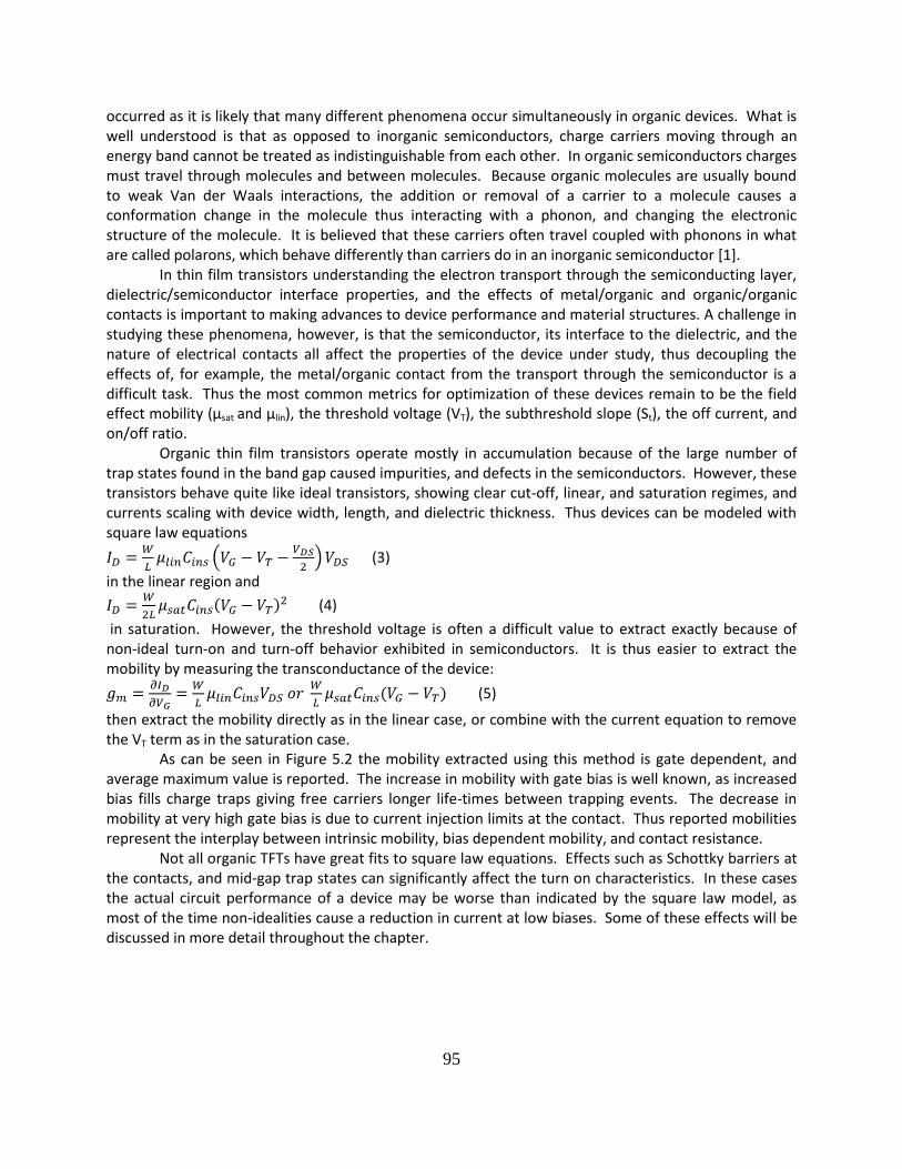
95
occurred as it is likely that many different phenomena occur simultaneously in organic devices. What is well understood is that as opposed to inorganic semiconductors, charge carriers moving through an energy band cannot be treated as indistinguishable from each other. In organic semiconductors charges must travel through molecules and between molecules. Because organic molecules are usually bound to weak Van der Waals interactions, the addition or removal of a carrier to a molecule causes a conformation change in the molecule thus interacting with a phonon, and changing the electronic structure of the molecule. It is believed that these carriers often travel coupled with phonons in what are called polarons, which behave differently than carriers do in an inorganic semiconductor [1]. In thin film transistors understanding the electron transport through the semiconducting layer, dielectric/semiconductor interface properties, and the effects of metal/organic and organic/organic contacts is important to making advances to device performance and material structures. A challenge in studying these phenomena, however, is that the semiconductor, its interface to the dielectric, and the nature of electrical contacts all affect the properties of the device under study, thus decoupling the effects of, for example, the metal/organic contact from the transport through the semiconductor is a difficult task. Thus the most common metrics for optimization of these devices remain to be the field effect mobility (μsat and μlin), the threshold voltage (VT), the subthreshold slope (St), the off current, and on/off ratio. Organic thin film transistors operate mostly in accumulation because of the large number of trap states found in the band gap caused impurities, and defects in the semiconductors. However, these transistors behave quite like ideal transistors, showing clear cut-off, linear, and saturation regimes, and currents scaling with device width, length, and dielectric thickness. Thus devices can be modeled with square law equations
(3)
in the linear region and
(4)
in saturation. However, the threshold voltage is often a difficult value to extract exactly because of non-ideal turn-on and turn-off behavior exhibited in semiconductors. It is thus easier to extract the mobility by measuring the transconductance of the device:
(5)
then extract the mobility directly as in the linear case, or combine with the current equation to remove the VT term as in the saturation case. As can be seen in Figure 5.2 the mobility extracted using this method is gate dependent, and average maximum value is reported. The increase in mobility with gate bias is well known, as increased bias fills charge traps giving free carriers longer life-times between trapping events. The decrease in mobility at very high gate bias is due to current injection limits at the contact. Thus reported mobilities represent the interplay between intrinsic mobility, bias dependent mobility, and contact resistance. Not all organic TFTs have great fits to square law equations. Effects such as Schottky barriers at the contacts, and mid-gap trap states can significantly affect the turn on characteristics. In these cases the actual circuit performance of a device may be worse than indicated by the square law model, as most of the time non-idealities cause a reduction in current at low biases. Some of these effects will be discussed in more detail throughout the chapter.

96
Figure 5.2. Transfer and output characteristics (top), and measured transconductance and mobility vs. gate bias for a pBTTT TFT made on SiO2. W=250 μm L=10 μm .
5.2 pBTTT and other modern polymer semiconductors Thanks to many advances over the years, organic semiconductors have been shown to exhibit electronic performance close to that of a-Si:H. However, one of the main challenges that have kept organic electronics from obtaining widespread use is a lack of stability to oxygen, moisture, and light exposure [2][3]. It is understood that electrochemical oxidation of organic semiconductors is a key component of their instability to air and moisture. This oxidative process occurs readily in air due to the low amount of energy required to withdraw an electron from the semiconductor and transfer it to an electron withdrawing oxygen species. This electron withdrawal energy is directly correlated to the ionization potential of the semiconductor, which in turn is equivalent to the HOMO level height. De Leeuw and co-workers established that the HOMO level must be at least 4.9eV from the vacuum level so that the oxidation process is unfavorable at room temperature [4]. However, synthesizing molecules that exhibit this band alignment has been a challenge, which has only recently been met for both p-type [5] and n-type materials [6]. The seminal work by McCulloch and Heeney, not only demonstrated that stability of organic semiconductors can be achieved through careful synthesis, but also that electronic performance need not be sacrificed [5]. Focused on the use of thiophene based polymers, the most studied class of p-type
-3.E-05
-2.E-05
-2.E-05
-1.E-05
-5.E-06
0.E+00
-40.00-30.00-20.00-10.000.00
ID[A
]
VD [V]
VG=0V
VG=-10V
VG=-20V
VG=-30V
VG=-40V
1.E-12
1.E-11
1.E-10
1.E-09
1.E-08
1.E-07
1.E-06
1.E-05
1.E-04
0.E+00
1.E-03
2.E-03
3.E-03
4.E-03
5.E-03
6.E-03
7.E-03
-40-30-20-10010
|ID| [
A]
Sq
rt |I
D| [
A^1/2
]
VG [V]
Sqrt |ID|
Vt
|ID|
St
0.E+0
2.E-7
4.E-7
6.E-7
8.E-7
1.E-6
1.E-6
1.E-6
2.E-6
0.E+0
1.E-2
2.E-2
3.E-2
4.E-2
5.E-2
6.E-2
7.E-2
8.E-2
9.E-2
1.E-1
-40-20020
gm
(S
)
(cm
^2/V
s)
VG (V)
mu
rough mu
sq law mu
gm
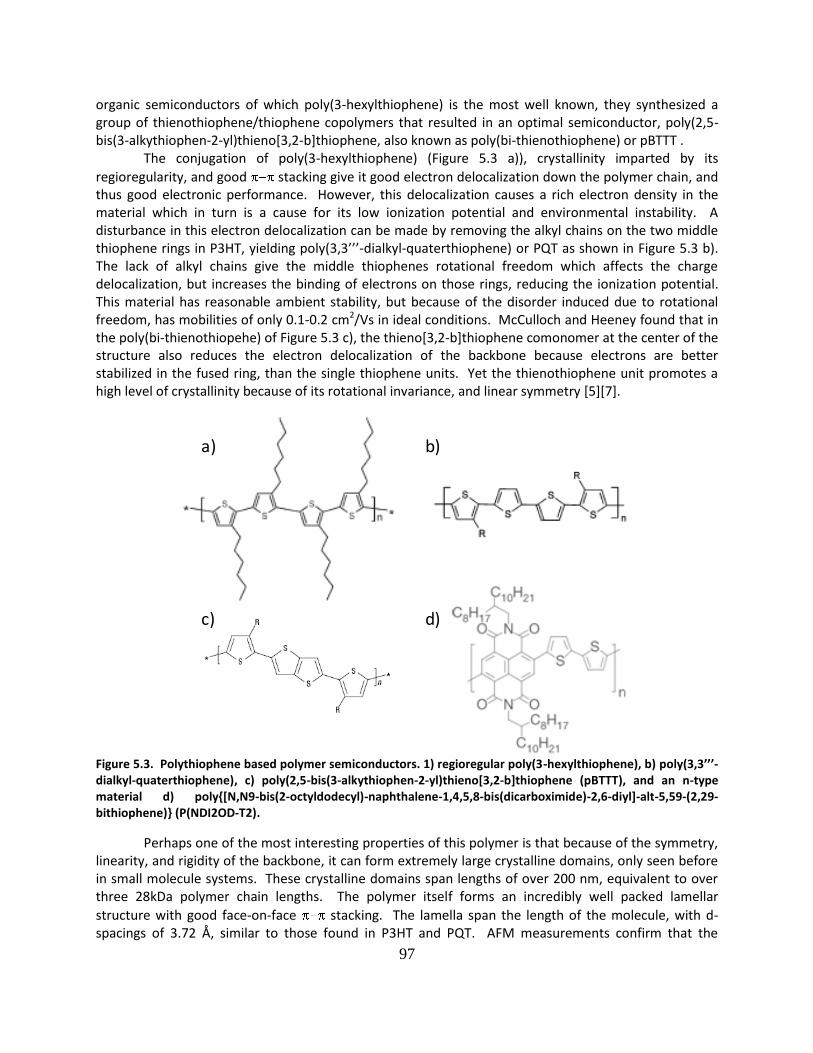
97
organic semiconductors of which poly(3-hexylthiophene) is the most well known, they synthesized a group of thienothiophene/thiophene copolymers that resulted in an optimal semiconductor, poly(2,5-bis(3-alkythiophen-2-yl)thieno[3,2-b]thiophene, also known as poly(bi-thienothiophene) or pBTTT . The conjugation of poly(3-hexylthiophene) (Figure 5.3 a)), crystallinity imparted by its
regioregularity, and good stacking give it good electron delocalization down the polymer chain, and thus good electronic performance. However, this delocalization causes a rich electron density in the material which in turn is a cause for its low ionization potential and environmental instability. A disturbance in this electron delocalization can be made by removing the alkyl chains on the two middle thiophene rings in P3HT, yielding poly(3,3’’’-dialkyl-quaterthiophene) or PQT as shown in Figure 5.3 b). The lack of alkyl chains give the middle thiophenes rotational freedom which affects the charge delocalization, but increases the binding of electrons on those rings, reducing the ionization potential. This material has reasonable ambient stability, but because of the disorder induced due to rotational freedom, has mobilities of only 0.1-0.2 cm2/Vs in ideal conditions. McCulloch and Heeney found that in the poly(bi-thienothiopehe) of Figure 5.3 c), the thieno[3,2-b]thiophene comonomer at the center of the structure also reduces the electron delocalization of the backbone because electrons are better stabilized in the fused ring, than the single thiophene units. Yet the thienothiophene unit promotes a high level of crystallinity because of its rotational invariance, and linear symmetry [5][7].
Figure 5.3. Polythiophene based polymer semiconductors. 1) regioregular poly(3-hexylthiophene), b) poly(3,3’’’-dialkyl-quaterthiophene), c) poly(2,5-bis(3-alkythiophen-2-yl)thieno[3,2-b]thiophene (pBTTT), and an n-type material d) poly{[N,N9-bis(2-octyldodecyl)-naphthalene-1,4,5,8-bis(dicarboximide)-2,6-diyl]-alt-5,59-(2,29-bithiophene)} (P(NDI2OD-T2).
Perhaps one of the most interesting properties of this polymer is that because of the symmetry, linearity, and rigidity of the backbone, it can form extremely large crystalline domains, only seen before in small molecule systems. These crystalline domains span lengths of over 200 nm, equivalent to over three 28kDa polymer chain lengths. The polymer itself forms an incredibly well packed lamellar
structure with good face-on-face stacking. The lamella span the length of the molecule, with d-spacings of 3.72 Å, similar to those found in P3HT and PQT. AFM measurements confirm that the
a) b)
c) d)
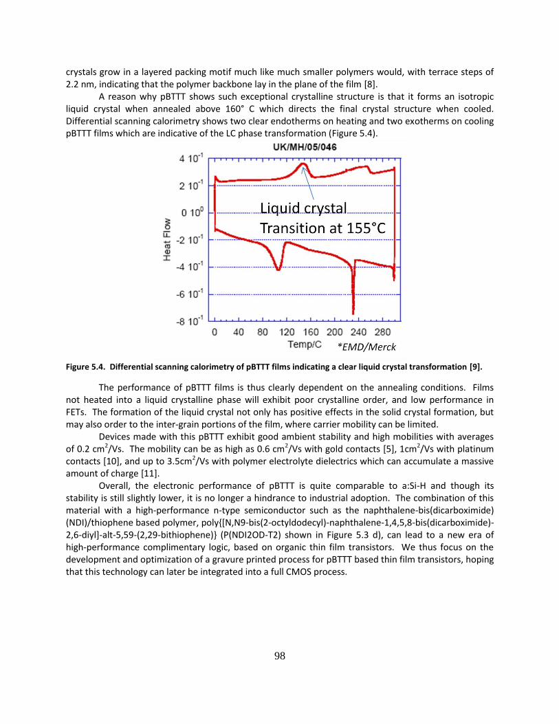
98
crystals grow in a layered packing motif much like much smaller polymers would, with terrace steps of 2.2 nm, indicating that the polymer backbone lay in the plane of the film [8]. A reason why pBTTT shows such exceptional crystalline structure is that it forms an isotropic liquid crystal when annealed above 160° C which directs the final crystal structure when cooled. Differential scanning calorimetry shows two clear endotherms on heating and two exotherms on cooling pBTTT films which are indicative of the LC phase transformation (Figure 5.4).
Figure 5.4. Differential scanning calorimetry of pBTTT films indicating a clear liquid crystal transformation [9].
The performance of pBTTT films is thus clearly dependent on the annealing conditions. Films not heated into a liquid crystalline phase will exhibit poor crystalline order, and low performance in FETs. The formation of the liquid crystal not only has positive effects in the solid crystal formation, but may also order to the inter-grain portions of the film, where carrier mobility can be limited. Devices made with this pBTTT exhibit good ambient stability and high mobilities with averages of 0.2 cm2/Vs. The mobility can be as high as 0.6 cm2/Vs with gold contacts [5], 1cm2/Vs with platinum contacts [10], and up to 3.5cm2/Vs with polymer electrolyte dielectrics which can accumulate a massive amount of charge [11]. Overall, the electronic performance of pBTTT is quite comparable to a:Si-H and though its stability is still slightly lower, it is no longer a hindrance to industrial adoption. The combination of this material with a high-performance n-type semiconductor such as the naphthalene-bis(dicarboximide) (NDI)/thiophene based polymer, poly{[N,N9-bis(2-octyldodecyl)-naphthalene-1,4,5,8-bis(dicarboximide)-2,6-diyl]-alt-5,59-(2,29-bithiophene)} (P(NDI2OD-T2) shown in Figure 5.3 d), can lead to a new era of high-performance complimentary logic, based on organic thin film transistors. We thus focus on the development and optimization of a gravure printed process for pBTTT based thin film transistors, hoping that this technology can later be integrated into a full CMOS process.
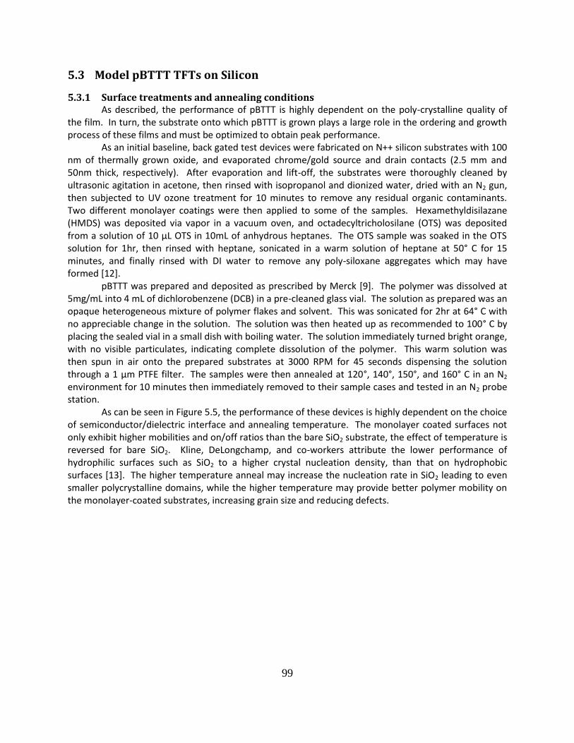
99
5.3 Model pBTTT TFTs on Silicon
5.3.1 Surface treatments and annealing conditions As described, the performance of pBTTT is highly dependent on the poly-crystalline quality of the film. In turn, the substrate onto which pBTTT is grown plays a large role in the ordering and growth process of these films and must be optimized to obtain peak performance. As an initial baseline, back gated test devices were fabricated on N++ silicon substrates with 100 nm of thermally grown oxide, and evaporated chrome/gold source and drain contacts (2.5 mm and 50nm thick, respectively). After evaporation and lift-off, the substrates were thoroughly cleaned by ultrasonic agitation in acetone, then rinsed with isopropanol and dionized water, dried with an N2 gun, then subjected to UV ozone treatment for 10 minutes to remove any residual organic contaminants. Two different monolayer coatings were then applied to some of the samples. Hexamethyldisilazane (HMDS) was deposited via vapor in a vacuum oven, and octadecyltricholosilane (OTS) was deposited from a solution of 10 μL OTS in 10mL of anhydrous heptanes. The OTS sample was soaked in the OTS solution for 1hr, then rinsed with heptane, sonicated in a warm solution of heptane at 50° C for 15 minutes, and finally rinsed with DI water to remove any poly-siloxane aggregates which may have formed [12]. pBTTT was prepared and deposited as prescribed by Merck [9]. The polymer was dissolved at 5mg/mL into 4 mL of dichlorobenzene (DCB) in a pre-cleaned glass vial. The solution as prepared was an opaque heterogeneous mixture of polymer flakes and solvent. This was sonicated for 2hr at 64° C with no appreciable change in the solution. The solution was then heated up as recommended to 100° C by placing the sealed vial in a small dish with boiling water. The solution immediately turned bright orange, with no visible particulates, indicating complete dissolution of the polymer. This warm solution was then spun in air onto the prepared substrates at 3000 RPM for 45 seconds dispensing the solution through a 1 μm PTFE filter. The samples were then annealed at 120°, 140°, 150°, and 160° C in an N2 environment for 10 minutes then immediately removed to their sample cases and tested in an N2 probe station. As can be seen in Figure 5.5, the performance of these devices is highly dependent on the choice of semiconductor/dielectric interface and annealing temperature. The monolayer coated surfaces not only exhibit higher mobilities and on/off ratios than the bare SiO2 substrate, the effect of temperature is reversed for bare SiO2. Kline, DeLongchamp, and co-workers attribute the lower performance of hydrophilic surfaces such as SiO2 to a higher crystal nucleation density, than that on hydrophobic surfaces [13]. The higher temperature anneal may increase the nucleation rate in SiO2 leading to even smaller polycrystalline domains, while the higher temperature may provide better polymer mobility on the monolayer-coated substrates, increasing grain size and reducing defects.
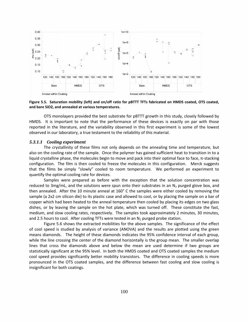
100
Figure 5.5. Saturation mobility (left) and on/off ratio for pBTTT TFTs fabricated on HMDS coated, OTS coated, and bare SiO2, and annealed at various temperatures.
OTS monolayers provided the best substrate for pBTTT growth in this study, closely followed by HMDS. It is important to note that the performance of these devices is exactly on par with those reported in the literature, and the variability observed in this first experiment is some of the lowest observed in our laboratory, a true testament to the reliability of this material.
5.3.1.1 Cooling experiment The crystallinity of these films not only depends on the annealing time and temperature, but also on the cooling rate of the sample. Once the polymer has gained sufficient heat to transition in to a liquid crystalline phase, the molecules begin to move and pack into their optimal face to face, π-stacking configuration. The film is then cooled to freeze the molecules in this configuration. Merck suggests that the films be simply “slowly” cooled to room temperature. We performed an experiment to quantify the optimal cooling rate for devices. Samples were prepared as before with the exception that the solution concentration was reduced to 3mg/mL, and the solutions were spun onto their substrates in an N2 purged glove box, and then annealed. After the 10 minute anneal at 160° C the samples were either cooled by removing the sample (a 2x2 cm silicon die) to its plastic case and allowed to cool, or by placing the sample on a bar of copper which had been heated to the anneal temperature then cooled by placing its edges on two glass dishes, or by leaving the sample on the hot plate, which was turned off. These constitute the fast, medium, and slow cooling rates, respectively. The samples took approximately 2 minutes, 30 minutes, and 2.5 hours to cool. After cooling TFTs were tested in an N2 purged probe station. Figure 5.6 shows the extracted mobilities for the above samples. The significance of the effect of cool speed is studied by analysis of variance (ANOVA) and the results are plotted using the green means diamonds. The height of these diamonds indicates the 95% confidence interval of each group, while the line crossing the center of the diamond horizontally is the group mean. The smaller overlap lines that cross the diamonds above and below the mean are used determine if two groups are statistically significant at the 95% level. In both the HMDS coated and OTS coated samples the medium cool speed provides significantly better mobility transistors. The difference in cooling speeds is more pronounced in the OTS coated samples, and the difference between fast cooling and slow cooling is insignificant for both coatings.
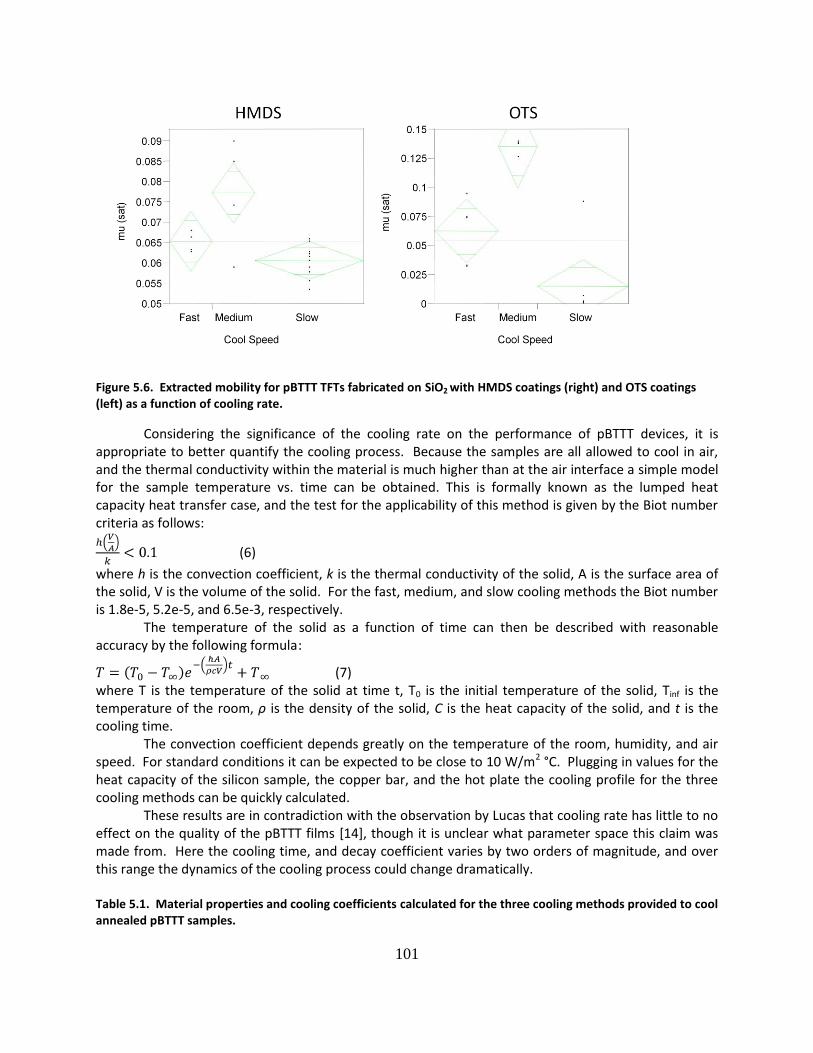
101
Figure 5.6. Extracted mobility for pBTTT TFTs fabricated on SiO2 with HMDS coatings (right) and OTS coatings (left) as a function of cooling rate.
Considering the significance of the cooling rate on the performance of pBTTT devices, it is appropriate to better quantify the cooling process. Because the samples are all allowed to cool in air, and the thermal conductivity within the material is much higher than at the air interface a simple model for the sample temperature vs. time can be obtained. This is formally known as the lumped heat capacity heat transfer case, and the test for the applicability of this method is given by the Biot number criteria as follows:
(6)
where h is the convection coefficient, k is the thermal conductivity of the solid, A is the surface area of the solid, V is the volume of the solid. For the fast, medium, and slow cooling methods the Biot number is 1.8e-5, 5.2e-5, and 6.5e-3, respectively. The temperature of the solid as a function of time can then be described with reasonable accuracy by the following formula:
(7) where T is the temperature of the solid at time t, T0 is the initial temperature of the solid, Tinf is the temperature of the room, ρ is the density of the solid, C is the heat capacity of the solid, and t is the cooling time. The convection coefficient depends greatly on the temperature of the room, humidity, and air speed. For standard conditions it can be expected to be close to 10 W/m2 °C. Plugging in values for the heat capacity of the silicon sample, the copper bar, and the hot plate the cooling profile for the three cooling methods can be quickly calculated. These results are in contradiction with the observation by Lucas that cooling rate has little to no effect on the quality of the pBTTT films [14], though it is unclear what parameter space this claim was made from. Here the cooling time, and decay coefficient varies by two orders of magnitude, and over this range the dynamics of the cooling process could change dramatically. Table 5.1. Material properties and cooling coefficients calculated for the three cooling methods provided to cool annealed pBTTT samples.
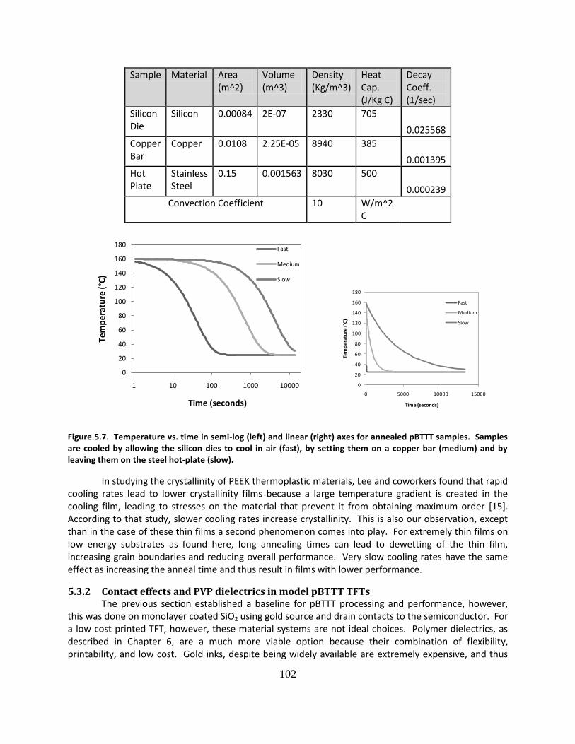
102
Sample Material Area (m^2)
Volume (m^3)
Density (Kg/m^3)
Heat Cap. (J/Kg C)
Decay Coeff. (1/sec)
Silicon Die
Silicon 0.00084 2E-07 2330 705
0.025568
Copper Bar
Copper 0.0108 2.25E-05 8940 385
0.001395
Hot Plate
Stainless Steel
0.15 0.001563 8030 500
0.000239
Convection Coefficient 10 W/m^2 C
Figure 5.7. Temperature vs. time in semi-log (left) and linear (right) axes for annealed pBTTT samples. Samples are cooled by allowing the silicon dies to cool in air (fast), by setting them on a copper bar (medium) and by leaving them on the steel hot-plate (slow).
In studying the crystallinity of PEEK thermoplastic materials, Lee and coworkers found that rapid cooling rates lead to lower crystallinity films because a large temperature gradient is created in the cooling film, leading to stresses on the material that prevent it from obtaining maximum order [15]. According to that study, slower cooling rates increase crystallinity. This is also our observation, except than in the case of these thin films a second phenomenon comes into play. For extremely thin films on low energy substrates as found here, long annealing times can lead to dewetting of the thin film, increasing grain boundaries and reducing overall performance. Very slow cooling rates have the same effect as increasing the anneal time and thus result in films with lower performance.
5.3.2 Contact effects and PVP dielectrics in model pBTTT TFTs The previous section established a baseline for pBTTT processing and performance, however, this was done on monolayer coated SiO2 using gold source and drain contacts to the semiconductor. For a low cost printed TFT, however, these material systems are not ideal choices. Polymer dielectrics, as described in Chapter 6, are a much more viable option because their combination of flexibility, printability, and low cost. Gold inks, despite being widely available are extremely expensive, and thus
0
20
40
60
80
100
120
140
160
180
1 10 100 1000 10000
Tem
pe
ratu
re (
°C)
Time (seconds)
Fast
Medium
Slow
0
20
40
60
80
100
120
140
160
180
0 5000 10000 15000
Tem
pe
ratu
re (°
C)
Time (seconds)
Fast
Medium
Slow
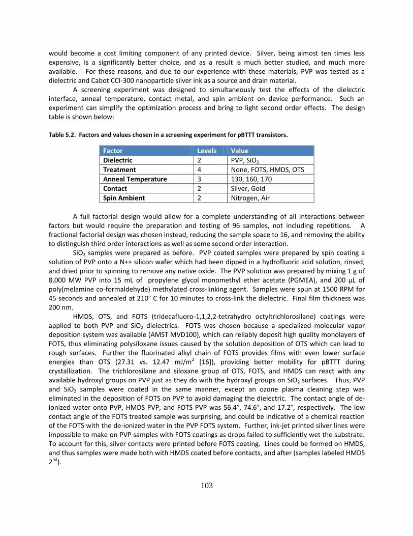
103
would become a cost limiting component of any printed device. Silver, being almost ten times less expensive, is a significantly better choice, and as a result is much better studied, and much more available. For these reasons, and due to our experience with these materials, PVP was tested as a dielectric and Cabot CCI-300 nanoparticle silver ink as a source and drain material. A screening experiment was designed to simultaneously test the effects of the dielectric interface, anneal temperature, contact metal, and spin ambient on device performance. Such an experiment can simplify the optimization process and bring to light second order effects. The design table is shown below: Table 5.2. Factors and values chosen in a screening experiment for pBTTT transistors.
Factor Levels Value
Dielectric 2 PVP, SiO2
Treatment 4 None, FOTS, HMDS, OTS
Anneal Temperature 3 130, 160, 170
Contact 2 Silver, Gold
Spin Ambient 2 Nitrogen, Air
A full factorial design would allow for a complete understanding of all interactions between factors but would require the preparation and testing of 96 samples, not including repetitions. A fractional factorial design was chosen instead, reducing the sample space to 16, and removing the ability to distinguish third order interactions as well as some second order interaction. SiO2 samples were prepared as before. PVP coated samples were prepared by spin coating a solution of PVP onto a N++ silicon wafer which had been dipped in a hydrofluoric acid solution, rinsed, and dried prior to spinning to remove any native oxide. The PVP solution was prepared by mixing 1 g of 8,000 MW PVP into 15 mL of propylene glycol monomethyl ether acetate (PGMEA), and 200 μL of poly(melamine co-formaldehyde) methylated cross-linking agent. Samples were spun at 1500 RPM for 45 seconds and annealed at 210° C for 10 minutes to cross-link the dielectric. Final film thickness was 200 nm. HMDS, OTS, and FOTS (tridecafluoro-1,1,2,2-tetrahydro octyltrichlorosilane) coatings were applied to both PVP and SiO2 dielectrics. FOTS was chosen because a specialized molecular vapor deposition system was available (AMST MVD100), which can reliably deposit high quality monolayers of FOTS, thus eliminating polysiloxane issues caused by the solution deposition of OTS which can lead to rough surfaces. Further the fluorinated alkyl chain of FOTS provides films with even lower surface energies than OTS (27.31 vs. 12.47 mJ/m2 [16]), providing better mobility for pBTTT during crystallization. The trichlorosilane and siloxane group of OTS, FOTS, and HMDS can react with any available hydroxyl groups on PVP just as they do with the hydroxyl groups on SiO2 surfaces. Thus, PVP and SiO2 samples were coated in the same manner, except an ozone plasma cleaning step was eliminated in the deposition of FOTS on PVP to avoid damaging the dielectric. The contact angle of de-ionized water onto PVP, HMDS PVP, and FOTS PVP was 56.4°, 74.6°, and 17.2°, respectively. The low contact angle of the FOTS treated sample was surprising, and could be indicative of a chemical reaction of the FOTS with the de-ionized water in the PVP FOTS system. Further, ink-jet printed silver lines were impossible to make on PVP samples with FOTS coatings as drops failed to sufficiently wet the substrate. To account for this, silver contacts were printed before FOTS coating. Lines could be formed on HMDS, and thus samples were made both with HMDS coated before contacts, and after (samples labeled HMDS 2nd).
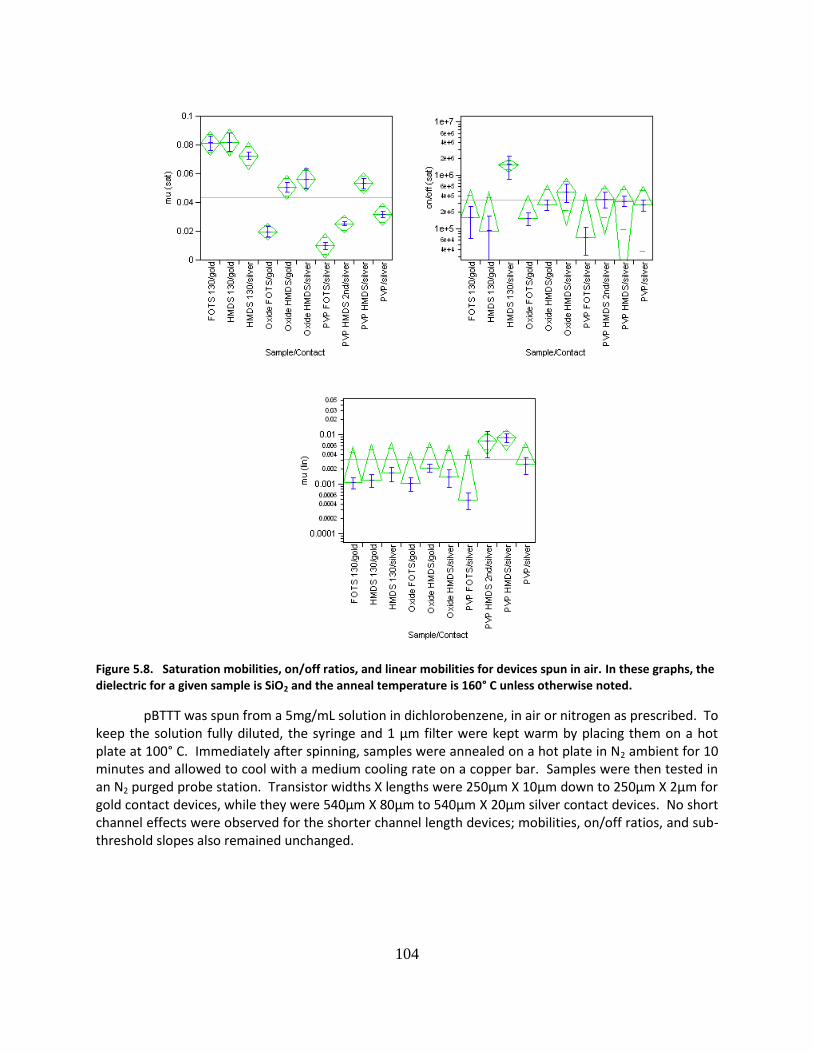
104
Figure 5.8. Saturation mobilities, on/off ratios, and linear mobilities for devices spun in air. In these graphs, the dielectric for a given sample is SiO2 and the anneal temperature is 160° C unless otherwise noted.
pBTTT was spun from a 5mg/mL solution in dichlorobenzene, in air or nitrogen as prescribed. To keep the solution fully diluted, the syringe and 1 μm filter were kept warm by placing them on a hot plate at 100° C. Immediately after spinning, samples were annealed on a hot plate in N2 ambient for 10 minutes and allowed to cool with a medium cooling rate on a copper bar. Samples were then tested in an N2 purged probe station. Transistor widths X lengths were 250μm X 10μm down to 250μm X 2μm for gold contact devices, while they were 540μm X 80μm to 540μm X 20μm silver contact devices. No short channel effects were observed for the shorter channel length devices; mobilities, on/off ratios, and sub-threshold slopes also remained unchanged.

105
Figure 5.9. Saturation mobilities, on/off ratios, and linear mobilities for devices spun in nitrogen. In these graphs, the dielectric for a given sample is SiO2 and the anneal temperature is 160° C unless otherwise noted.
Saturation mobility, linear mobility, and on/off ratios for these devices are arranged in two different ways in the following figures. Figure 5.8 presents data for devices spun in air, Figure 5.9, presents data for devices spun in nitrogen. This allows an easy comparison of the effects of dielectric, surface treatment and contact. To better see the effects of spinning in nitrogen, Figure 5.10 and Figure 5.11 present data for devices with gold contacts and silver contacts separately. One of the most notable findings in this study is that ink-jet printed silver contacts can provide TFTs of equivalent performance to devices with gold contacts, despite a significant work-function difference between the two metals, and the HOMO level of the semiconductor. No significant difference in saturation mobility or on/off ratio can be found between silver and gold contact HMDS oxide samples regardless if they were spun in air (Figure 5.8) or nitrogen (Figure 5.9). However, for both spin conditions, silver contact samples provide significantly higher linear mobilities.
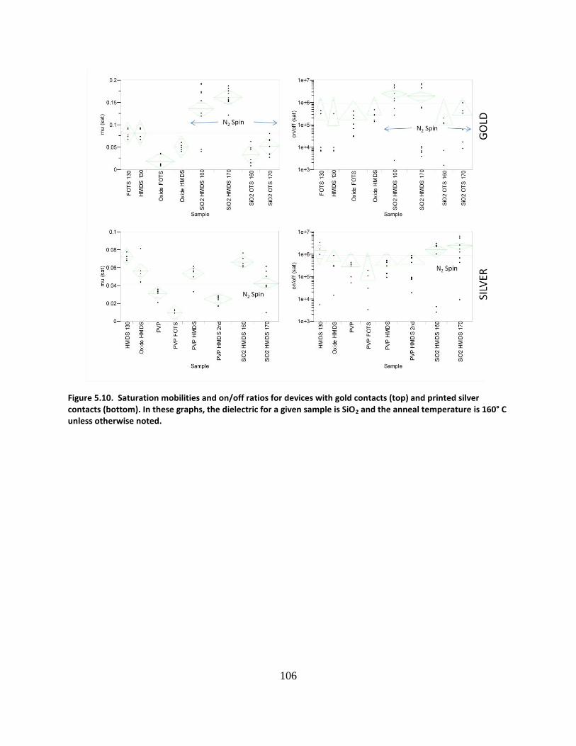
106
Figure 5.10. Saturation mobilities and on/off ratios for devices with gold contacts (top) and printed silver contacts (bottom). In these graphs, the dielectric for a given sample is SiO2 and the anneal temperature is 160° C unless otherwise noted.
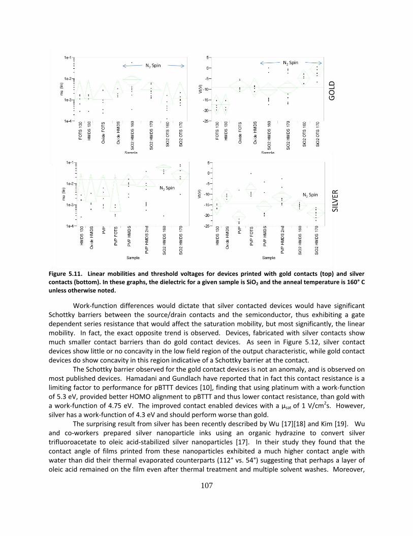
107
Figure 5.11. Linear mobilities and threshold voltages for devices printed with gold contacts (top) and silver contacts (bottom). In these graphs, the dielectric for a given sample is SiO2 and the anneal temperature is 160° C unless otherwise noted.
Work-function differences would dictate that silver contacted devices would have significant Schottky barriers between the source/drain contacts and the semiconductor, thus exhibiting a gate dependent series resistance that would affect the saturation mobility, but most significantly, the linear mobility. In fact, the exact opposite trend is observed. Devices, fabricated with silver contacts show much smaller contact barriers than do gold contact devices. As seen in Figure 5.12, silver contact devices show little or no concavity in the low field region of the output characteristic, while gold contact devices do show concavity in this region indicative of a Schottky barrier at the contact. The Schottky barrier observed for the gold contact devices is not an anomaly, and is observed on most published devices. Hamadani and Gundlach have reported that in fact this contact resistance is a limiting factor to performance for pBTTT devices [10], finding that using platinum with a work-function of 5.3 eV, provided better HOMO alignment to pBTTT and thus lower contact resistance, than gold with a work-function of 4.75 eV. The improved contact enabled devices with a μsat of 1 V/cm2s. However, silver has a work-function of 4.3 eV and should perform worse than gold. The surprising result from silver has been recently described by Wu [17][18] and Kim [19]. Wu and co-workers prepared silver nanoparticle inks using an organic hydrazine to convert silver trifluoroacetate to oleic acid-stabilized silver nanoparticles [17]. In their study they found that the contact angle of films printed from these nanoparticles exhibited a much higher contact angle with water than did their thermal evaporated counterparts (112° vs. 54°) suggesting that perhaps a layer of oleic acid remained on the film even after thermal treatment and multiple solvent washes. Moreover,

108
they fabricated TFTs with three contacts materials – their oleic acid stabilized silver nanoparticles, oleylamine-stabilized silver nanoparticles, and evaporated silver – and the polythiophene based semiconductor PQT-12. As with our observations, they found that the oleic-acid stabilized nanoparticles provided transistors with significantly lower contact barriers than either the oleylamine-stabilized, or thermally evaporated silver films, concluding that the oleic acid stabilizer was acting as a molecular doping to the semiconductor, creating an ohmic contact at the interface, despite a large metal work-function to HOMO level mismatch (4.3eV to 5.2eV). In a later study, the same group reported similar results for silver-salt based inks which again contained the oleic-aid stabilizer [18].
Figure 5.12. Transfer (top) and output (bottom) characteristics for pBTTT transistors fabricated on HMDS oxide with gold contacts (left) and silver contacts (right). μsat=.12 and .06, on/off = 5e6 and 3e6, μlin=3.5e-3 and 3.7e-2 for gold and silver contact devices, respectively. Insets show good square law behavior for both devices, and curves used to extract VT (-15 V for gold, -13 V for silver) and subthreshold slopes (0.76 V/dec for gold and 1.12 V/dec for silver).
Kim and co-workers found similar results to Wu’s and those presented here using a slightly different material system. They used poly(vinyl pyrrolidone) stabilized silver nanoparticles to print silver contacts for TFTs fabricated with dihexylquarterhiopene (DH4T) as a semiconductor. Using the transmission line method, they measured contact resistances for devices made with nanoparticle contacts, and evaporated contacts, and found a 5x decrease in contact resistance by nanoparticle lines annealed at 200° C and above versus the evaporated silver electrodes. Using x-ray photoemission spectroscopy (XPS) and ultraviolet photoemission spectroscopy (UPS) they determined that the shift in metal work-function was caused by chemisorbed poly(vinyl-pyrrolidone), which then decomposed to leave behind a coordinate bonded oxygen that induced a large surface dipole, increasing the effective work-function (Figure 5.13). Another important finding from this screening experiment is that PVP can be optimized to yield devices of comparable performance to those with SiO2 dielectrics. However, as with SiO2 PVP must be treated with HMDS to yield adequate performance. Figure 5.8 and Figure 5.10 show that while devices
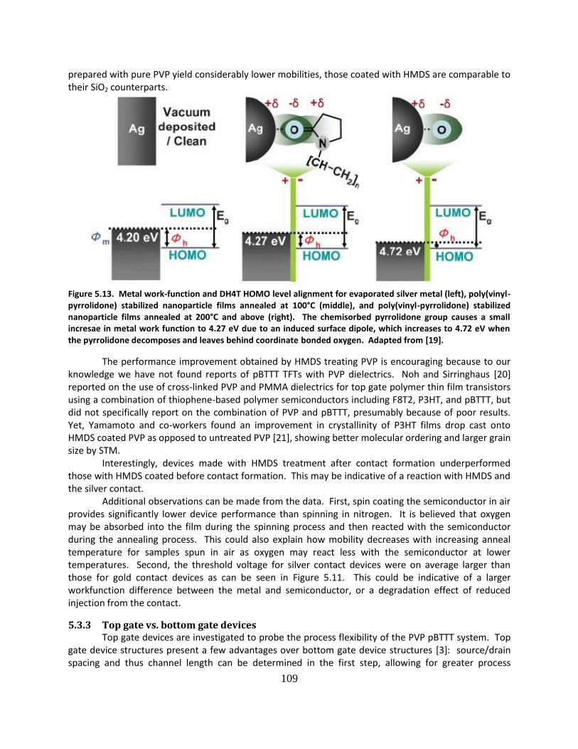
109
prepared with pure PVP yield considerably lower mobilities, those coated with HMDS are comparable to their SiO2 counterparts.
Figure 5.13. Metal work-function and DH4T HOMO level alignment for evaporated silver metal (left), poly(vinyl-pyrrolidone) stabilized nanoparticle films annealed at 100°C (middle), and poly(vinyl-pyrrolidone) stabilized nanoparticle films annealed at 200°C and above (right). The chemisorbed pyrrolidone group causes a small incresae in metal work function to 4.27 eV due to an induced surface dipole, which increases to 4.72 eV when the pyrrolidone decomposes and leaves behind coordinate bonded oxygen. Adapted from [19].
The performance improvement obtained by HMDS treating PVP is encouraging because to our knowledge we have not found reports of pBTTT TFTs with PVP dielectrics. Noh and Sirringhaus [20] reported on the use of cross-linked PVP and PMMA dielectrics for top gate polymer thin film transistors using a combination of thiophene-based polymer semiconductors including F8T2, P3HT, and pBTTT, but did not specifically report on the combination of PVP and pBTTT, presumably because of poor results. Yet, Yamamoto and co-workers found an improvement in crystallinity of P3HT films drop cast onto HMDS coated PVP as opposed to untreated PVP [21], showing better molecular ordering and larger grain size by STM. Interestingly, devices made with HMDS treatment after contact formation underperformed those with HMDS coated before contact formation. This may be indicative of a reaction with HMDS and the silver contact. Additional observations can be made from the data. First, spin coating the semiconductor in air provides significantly lower device performance than spinning in nitrogen. It is believed that oxygen may be absorbed into the film during the spinning process and then reacted with the semiconductor during the annealing process. This could also explain how mobility decreases with increasing anneal temperature for samples spun in air as oxygen may react less with the semiconductor at lower temperatures. Second, the threshold voltage for silver contact devices were on average larger than those for gold contact devices as can be seen in Figure 5.11. This could be indicative of a larger workfunction difference between the metal and semiconductor, or a degradation effect of reduced injection from the contact.
5.3.3 Top gate vs. bottom gate devices Top gate devices are investigated to probe the process flexibility of the PVP pBTTT system. Top gate device structures present a few advantages over bottom gate device structures [3]: source/drain spacing and thus channel length can be determined in the first step, allowing for greater process
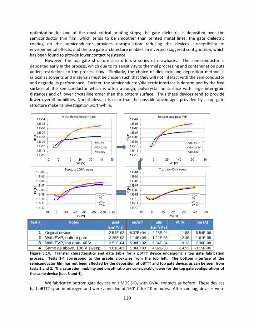
110
optimization for one of the most critical printing steps; the gate dielectric is deposited over the semiconductor thin film, which tends to be smoother than printed metal lines; the gate dielectric coating on the semiconductor provides encapsulation reducing the devices susceptibility to environmental effects; and the top gate architecture enables an inverted staggered configuration, which has been found to provide lower contact resistance. However, the top gate structure also offers a series of drawbacks. The semiconductor is deposited early in the process, which due to its sensitivity to thermal processing and contamination puts added restrictions to the process flow. Similarly, the choice of dielectric and deposition method is critical as solvents and materials must be chosen such that they will not interact with the semiconductor and degrade its performance. Further, the semiconductor/dielectric interface is determined by the free surface of the semiconductor which is often a rough, polycrystalline surface with large inter-grain distances and of lower crystalline order than the bottom surface. Thus these devices tend to provide lower overall mobilities. Nonetheless, it is clear that the possible advantages provided by a top gate structure make its investigation worthwhile.
Test # Notes μsat
(cm2/V s)
on/off μlin (cm
2/V s)
Vt (V) Ion (A)
1 Original device 2.54E-02 8.37E+04 4.25E-04 -11.88 -5.54E-06
2 With PVP, bottom gate 2.25E-02 1.14E+05 1.22E-03 -12.46 -1.61E-05
3 With PVP, top gate, 40 V 3.52E-04 5.38E+02 5.34E-04 -9.13 -7.30E-08
4 Same as above, 100 V sweep 3.01E-03 1.36E+03 4.02E-03 -14.53 -3.15E-06
Figure 5.14. Transfer characteristics and data table for a pBTTT device undergoing a top gate fabrication process. Tests 1-4 correspond to the graphs clockwise from the top left. The bottom interface of the semiconductor film has not been affected by the deposition of pBTTT and top gate device, as can be seen from tests 1 and 2. The saturation mobility and on/off ratio are considerably lower for the top gate configurations of the same device (test 3 and 4).
We fabricated bottom gate devices on HMDS SiO2 with Cr/Au contacts as before. These devices had pBTTT spun in nitrogen and were annealed at 160° C for 10 minutes. After cooling, devices were

111
tested in an N2 probe station, then coated with a solution of 1g PVP in 15 mL of hexanol with 200 μL of melamine cross-linker at 2000 RPM for 30 seconds. Hexanol was chosen as a solvent because PVP inks prepared in PGMEA solvent dewet the semiconductor. A sample with only half of its devices coated with PVP and a sample without any PVP treatment were prepared as controls, and sent through the same heating and printing process steps as the test sample. After coating with PVP, devices were annealed at 210° C in N2 for 10 minutes to cross-link the dielectric. Devices were again tested and no noticeable loss of performance was found. Gate contacts were then ink-jet printed with Cabot CCI-300 nanoparticle ink in air, and annealed at 150° C for 20 minutes in N2. Again, bottom gate devices remained unaltered (Figure 5.14). Finally, the top gate configuration was tested by removing contacts to the silicon back-gate and probing the ink-jet printed top-gate. Unfortunately, the top gate configuration exhibited low on current and low saturation mobilities, despite having low leakage. The output characteristics for devices in the top gate configuration show a very clean cut-off, and relatively straight linear region, indicating that the current in this device is channel dominated (Figure 5.15). The bottom gate configuration, on the other hand shows a considerably higher on current than the top gate configuration thanks to better mobility at that semiconductor interface. A number of explanations can be found for the large discrepancy in mobility between the top gate and bottom gate configurations. As mentioned, the surface roughness of the top surface of the semiconductor could definitely be a major factor in reducing the carrier mobility. Additionally, we have demonstrated that pBTTT shows lower performance when interfaced with pure PVP dielectrics as is the case with the top gate structure where it is not possible to HMDS treat the semiconductor/dielectric interface. Further, this test has not completely ruled out deleterious effects of solvent interactions and contamination of the semiconductor due to processing as those effects may have not diffused far enough to damage the bottom interface of the semiconductor.
Figure 5.15. Output characteristics for a pBTTT device tested in bottom gate configuration (left), and top gate configuration (right).
Though this test has shown that top gated pBTTT devices fabricated with PVP as a dielectric are inferior to their bottom gate counterparts, it has shown that bottom gate pBTTT devices can withstand a high level of thermal processing, and can be successfully encapsulated by PVP without any appreciable loss to performance.
5.3.4 Ink-jet printed pBTTT The major benefit of most polymeric semiconductors over their small-molecule counterparts is the ease with which they can be solubilized into a variety of organic solvents, and deposited via various printing methods. The length of these polymers and their inherent disorder facilitate their solubility, but
-6.E-06
-5.E-06
-4.E-06
-3.E-06
-2.E-06
-1.E-06
0.E+00
-40.00-30.00-20.00-10.000.00
ID[A
]
VD [V]
Bottom Gate
VG=0V
VG=-10VVG=-20VVG=-30V
-3.E-07
-2.E-07
-2.E-07
-1.E-07
-5.E-08
0.E+00
-40.00-30.00-20.00-10.000.00
ID[A
]
VD [V]
Top GateVG=0VVG=-10V
VG=-20VVG=-30V
112
also hinder their thin-film crystallinity. Small-molecules generally offer much better crystallinity, but their flat rigid structures make the molecules bind tightly to each other affecting their solubility. In order to overcome this solubility/crystallinity trade-off, several small molecules have been developed which have functional groups that sterically hinder the Van der Waals attractions between molecules so they can be easily dissolved. These functional groups are designed to be easily removed from the molecule by thermal decomposition, allowing the small-molecule to regain its tight-packing structure once heated; or to be positioned in such a matter that they do not hinder crystallinity upon solvent removal. pBTTT offers benefits of both small molecules and polymers, having the crystallinity only previously seen in small-molecules, yet allowing for better solubility. However, in practical terms pBTTT crystallizes so well that its solubility is considerably lower than most other polymer semiconductors and thus requires heating of the solvent to nearly 100° C to be solubilized. Upon cooling of the solution, the system forms a high viscosity gel which could potentially be printable, but contains a considerable number of crystallites that are formed during the gelling process, and which would compromise the overall uniformity of the film. Currently no alternative to solvent heating has been demonstrated to allow the formulation of pBTTT inks, so any printing technique employed must allow for the use of a heated ink. Fortunately, ink-jet had been demonstrated to be a viable technique for printing hot inks. Most notably, it has been used for printing molten solder [22] at temperatures up to 300° C. Despite its low-throughput, inkjet demonstrates good potential for a deposition technique for semiconductors. As a process it requires very small amounts of ink, and utilizes only as much ink as is patterned, making it useful for development but also minimizing waste in fabrication. As it is a non-contact method, it minimizes damage to bottom gate TFTs where the semiconductor is printed last. Further if the problem of satellite droplets can be avoided, ink-jet leaves no residue in the non-patterned areas, and with the use of multiple printing heads could deposit multiple materials in a single pass. This would be ideal for CMOS circuits where different n-type and p-type semiconductor must be deposited. A custom heated ink-jet printed system was developed to allow for the deposition of pBTTT. This system is comprised of a Microfab microjet piezo-electric printing system, a custom print-head heating unit and heated ink reservoir and ink delivery. A pBTTT ink was prepared as for spinning, and printed with an ink-jet head temperature of 100° C. Printing proved to be difficult as solvent evaporation at the nozzle increased the viscosity of the ink and clogged the head. In order to begin printing the printer nozzle had to be dipped in hot solvent to re-dissolve the polymer and re-establish jetting. As long as jetting was enabled, replenishing the nozzle with fresh ink, clogging could be avoided. However, this lead to reliability problems when print patterns required long periods of printer motion without jetting. Test devices were made using PVP on Si, and printed silver contacts. Because of the inability to reliably ink-jet print the material, thickness control was poor, and resulting devices exhibited extremely low mobilities, and a very large VT (-35 V) despite having a dielectric thickness of only 200 nm.

113
Figure 5.16. Transfer and output characteristics for a test TFT with PVP dielectric, ink-jet printed silver contacts, and ink-jet printed pBTTT. W=550 μm, L=28 μm, tPVP=200nm, μsat=1.2e-4 cm
2/Vs, on/off=5e3, μlin=7.5e-6 cm
2/Vs,
VT=-35 V, Von=-28 V.
Aside from the poor thickness control obtained in the ink-jet printing process, a few other factors undermined the performance of these devices. Printing was done in air, which due to the large surface area to volume ratio of the printed droplets could have resulted in a large amount of oxygen and moisture incorporated into the film. Further, the PVP in this experiment was not treated with HMDS limiting the performance of the semiconductor. With some technological improvements such as a heated solvent reservoir where the ink-jet head could be programmed to rest, and a nitrogen printing environment, it could be possible to improve the printability of pBTTT solutions, obtaining more uniform films and better performance.
5.4 Fully Printed Devices With optimal process parameters for annealing and crystallizing pBTTT films established, and tests made with PVP as a dielectric and printed nanoparticle silver as contacts, it has been shown that a printable material system can be used to fabricate high performance organic thin film transistors. These findings, along with the work presented in Chapter 5 on gravure printing thin, smooth, high-resolution metal lines, and the work presented in Chapter 6 on gravure printing thin film capacitors with PVP were used as a baseline to develop a process for gravure printed pBTTT thin film transistors. Yet to be demonstrated is a method for printing the pBTTT semiconductor that can provide comparable performance to spin coated films and any specific process steps required for integrating the established process modules. This is presented below.
5.4.1 Gravure printed pBTTT In an effort to overcome the challenges to printing pBTTT with ink-jet printing, the use of gravure as a deposition method was considered. Gravure rolls and doctor blades are metallic and thus impervious to organic solvents regardless of their temperatures, further they can be heated [23] to maintain a pBTTT ink dissolved and at a consistent viscosity. In a manufacturing environment the printing station could be purged in nitrogen and the ink delivery could be either a warm bath with the ink at its ideal temperature or an extrusion coater type device which would minimize solvent evaporation. In the laboratory, the gravure roll is heated prior to printing in an oven. Because of its high thermal mass, the roll can easily maintain its temperature to complete a print; ink is delivered to the nip from a heated syringe as for spinning. An electromechanically engraved gravure roll with 16 patterns,
1.E-12
1.E-11
1.E-10
1.E-09
1.E-08
1.E-07
1.E-06
1.E-05
1.E-04
-60-40-200
ID(A
)
VG (V)
VD=-5V
VD=-32.5V
VD=-60V
-3.E-08
-3.E-08
-2.E-08
-2.E-08
-1.E-08
-5.E-09
0.E+00
-60.00-50.00-40.00-30.00-20.00-10.000.00
ID(A
)
VD (V)
VG=0V
VG=-15V
VG=-30V
VG=-45V
VG=-60V
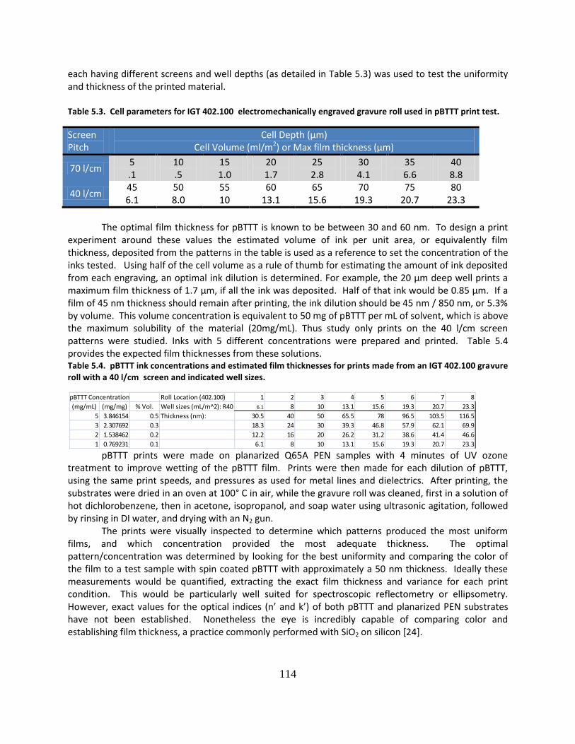
114
each having different screens and well depths (as detailed in Table 5.3) was used to test the uniformity and thickness of the printed material. Table 5.3. Cell parameters for IGT 402.100 electromechanically engraved gravure roll used in pBTTT print test.
Screen Pitch
Cell Depth (μm) Cell Volume (ml/m2) or Max film thickness (μm)
70 l/cm 5 .1
10 .5
15 1.0
20 1.7
25 2.8
30 4.1
35 6.6
40 8.8
40 l/cm 45 6.1
50 8.0
55 10
60 13.1
65 15.6
70 19.3
75 20.7
80 23.3
The optimal film thickness for pBTTT is known to be between 30 and 60 nm. To design a print experiment around these values the estimated volume of ink per unit area, or equivalently film thickness, deposited from the patterns in the table is used as a reference to set the concentration of the inks tested. Using half of the cell volume as a rule of thumb for estimating the amount of ink deposited from each engraving, an optimal ink dilution is determined. For example, the 20 μm deep well prints a maximum film thickness of 1.7 μm, if all the ink was deposited. Half of that ink would be 0.85 μm. If a film of 45 nm thickness should remain after printing, the ink dilution should be 45 nm / 850 nm, or 5.3% by volume. This volume concentration is equivalent to 50 mg of pBTTT per mL of solvent, which is above the maximum solubility of the material (20mg/mL). Thus study only prints on the 40 l/cm screen patterns were studied. Inks with 5 different concentrations were prepared and printed. Table 5.4 provides the expected film thicknesses from these solutions. Table 5.4. pBTTT ink concentrations and estimated film thicknesses for prints made from an IGT 402.100 gravure roll with a 40 l/cm screen and indicated well sizes.
pBTTT prints were made on planarized Q65A PEN samples with 4 minutes of UV ozone treatment to improve wetting of the pBTTT film. Prints were then made for each dilution of pBTTT, using the same print speeds, and pressures as used for metal lines and dielectrics. After printing, the substrates were dried in an oven at 100° C in air, while the gravure roll was cleaned, first in a solution of hot dichlorobenzene, then in acetone, isopropanol, and soap water using ultrasonic agitation, followed by rinsing in DI water, and drying with an N2 gun. The prints were visually inspected to determine which patterns produced the most uniform films, and which concentration provided the most adequate thickness. The optimal pattern/concentration was determined by looking for the best uniformity and comparing the color of the film to a test sample with spin coated pBTTT with approximately a 50 nm thickness. Ideally these measurements would be quantified, extracting the exact film thickness and variance for each print condition. This would be particularly well suited for spectroscopic reflectometry or ellipsometry. However, exact values for the optical indices (n’ and k’) of both pBTTT and planarized PEN substrates have not been established. Nonetheless the eye is incredibly capable of comparing color and establishing film thickness, a practice commonly performed with SiO2 on silicon [24].
Roll Location (402.100) 1 2 3 4 5 6 7 8
(mg/mL) (mg/mg) % Vol. Well sizes (mL/m^2): R40 6.1 8 10 13.1 15.6 19.3 20.7 23.3
5 3.846154 0.5 Thickness (nm): 30.5 40 50 65.5 78 96.5 103.5 116.5
3 2.307692 0.3 18.3 24 30 39.3 46.8 57.9 62.1 69.9
2 1.538462 0.2 12.2 16 20 26.2 31.2 38.6 41.4 46.6
1 0.769231 0.1 6.1 8 10 13.1 15.6 19.3 20.7 23.3
pBTTT Concentration

115
Figure 5.17. Apparent film thickness variation (top) and equivalent gravure cell spacing (bottom) for gravure printed pBTTT films. Large cells (a) merge in the vertical print direction causing band-like thickness variation. Small cells (c) are too far apart to allow ink to uniformly spread. An ideal cell spacing (b) allows for fluid flow to form uniform films.
Patterns printed with a high print volume (21 or 23 ml/m2) presented an oscillatory thickness perpendicular to the print direction but good uniformity in the print direction (Figure 5.17 (a)). Patterns printed with a low print volume (6 and 8 ml/m2) had an incomplete film as wells were spaced too far apart for the deposited ink to spread and merge. Patterns with a slightly higher print volume (10 ml/m2) were continuous films, but exhibited a similar color oscillation as the dithered patterns (Figure 5.17 (c)), while a few print volumes (13 and 15.6 ml/m2) yielded optically uniform films (Figure 5.17 (b)). Best results were found using a pBTTT concentration of 3mg/mL of pBTTT in DCB and a 13.1 mL/m2 pattern. At this point the printability of pBTTT with gravure has been established and print parameters optimized to yield thin, uniform films. Ideally, these films would be tested on a silicon test structure to confirm the semiconducting quality of the film independently from other print factors, but as discussed in Chapter 1, direct gravure is not amenable to printing on hard substrates; fully printed structures a thus fabricated.
5.4.2 A fully printed TFT process Having established process modules for thin gravure-printed metal lines suitable for both gates and contacts, a gravure printed capacitor with sufficient capacitance to be used as a gate stack for a TFT, ink-jet printed contacts, and a gravure printed semiconductor, both a bottom gate and top gate (staggered) process were designed for the fabrication of all-printed TFTs. The process flow is demonstrated in Figure 5.18 for both bottom gate devices (left) and top gate devices (right). Top gate transistors were printed despite having shown poor performance in our model devices because of their facile preparation and to rule out any unforeseen interactions from the printed process.
5.4.2.1 Bottom gate transistors In the bottom gate process (Figure 5.18 (left)), the gate and dielectric were printed as shown in Chapter 5 and 6. The gates were printed using Inktec PR-010, on planarized Q65FA PEN substrates,
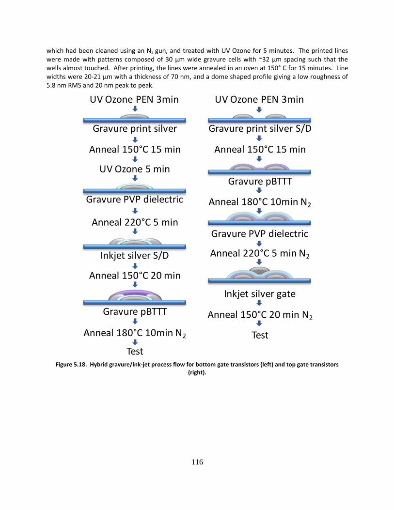
116
which had been cleaned using an N2 gun, and treated with UV Ozone for 5 minutes. The printed lines were made with patterns composed of 30 μm wide gravure cells with ~32 μm spacing such that the wells almost touched. After printing, the lines were annealed in an oven at 150° C for 15 minutes. Line widths were 20-21 μm with a thickness of 70 nm, and a dome shaped profile giving a low roughness of 5.8 nm RMS and 20 nm peak to peak.
Figure 5.18. Hybrid gravure/ink-jet process flow for bottom gate transistors (left) and top gate transistors
(right).
UV Ozone PEN 3min
Gravure print silver S/D
Anneal 150°C 15 min
Gravure PVP dielectric
Anneal 220°C 5 min N2
Inkjet silver gate
Anneal 150°C 20 min N2
Gravure pBTTT
Anneal 180°C 10min N2
Test
UV Ozone PEN 3min
Gravure print silver
Anneal 150°C 15 min
UV Ozone 5 min
Gravure PVP dielectric
Anneal 220°C 5 min
Inkjet silver S/D
Anneal 150°C 20 min
Gravure pBTTT
Anneal 180°C 10min N2
Test
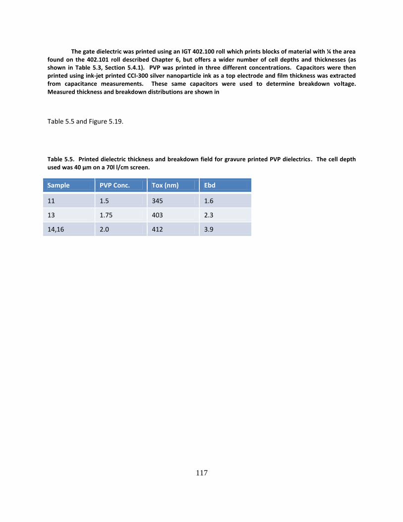
117
The gate dielectric was printed using an IGT 402.100 roll which prints blocks of material with ¼ the area found on the 402.101 roll described Chapter 6, but offers a wider number of cell depths and thicknesses (as shown in Table 5.3, Section 5.4.1). PVP was printed in three different concentrations. Capacitors were then printed using ink-jet printed CCI-300 silver nanoparticle ink as a top electrode and film thickness was extracted from capacitance measurements. These same capacitors were used to determine breakdown voltage. Measured thickness and breakdown distributions are shown in
Table 5.5 and Figure 5.19.
Table 5.5. Printed dielectric thickness and breakdown field for gravure printed PVP dielectrics. The cell depth used was 40 μm on a 70l l/cm screen.
Sample PVP Conc. Tox (nm) Ebd
11 1.5 345 1.6
13 1.75 403 2.3
14,16 2.0 412 3.9
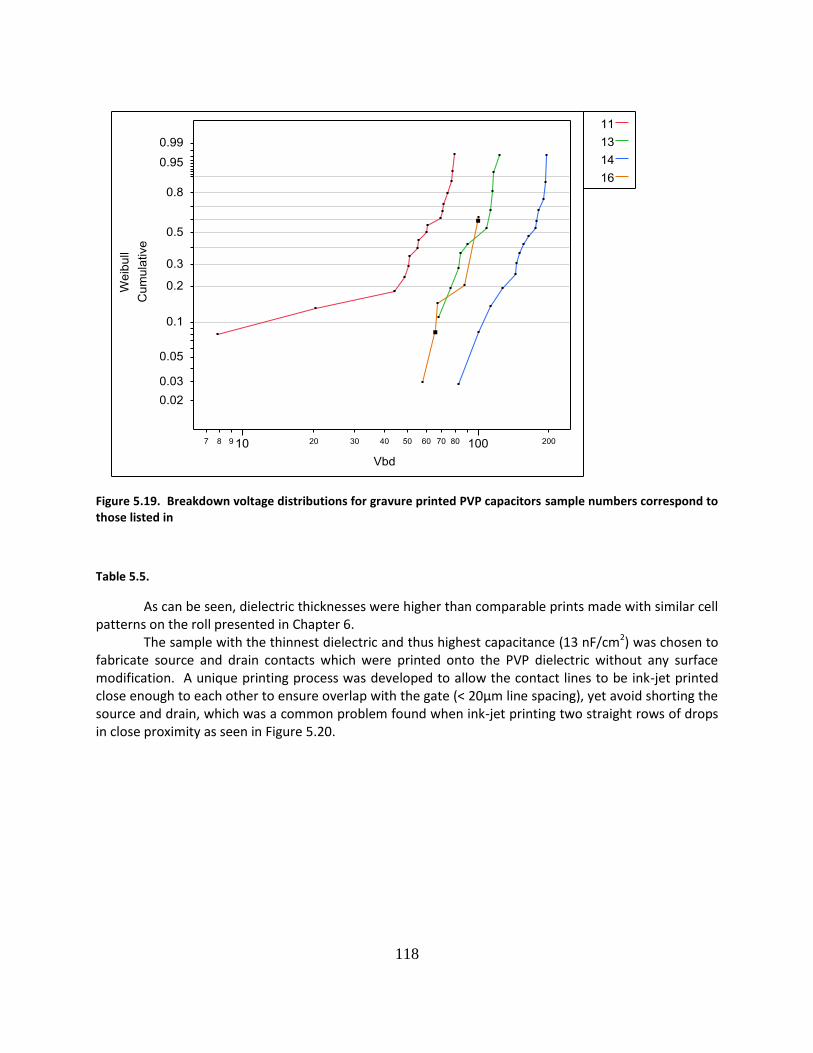
118
Figure 5.19. Breakdown voltage distributions for gravure printed PVP capacitors sample numbers correspond to those listed in
Table 5.5.
As can be seen, dielectric thicknesses were higher than comparable prints made with similar cell patterns on the roll presented in Chapter 6. The sample with the thinnest dielectric and thus highest capacitance (13 nF/cm2) was chosen to fabricate source and drain contacts which were printed onto the PVP dielectric without any surface modification. A unique printing process was developed to allow the contact lines to be ink-jet printed close enough to each other to ensure overlap with the gate (< 20μm line spacing), yet avoid shorting the source and drain, which was a common problem found when ink-jet printing two straight rows of drops in close proximity as seen in Figure 5.20.
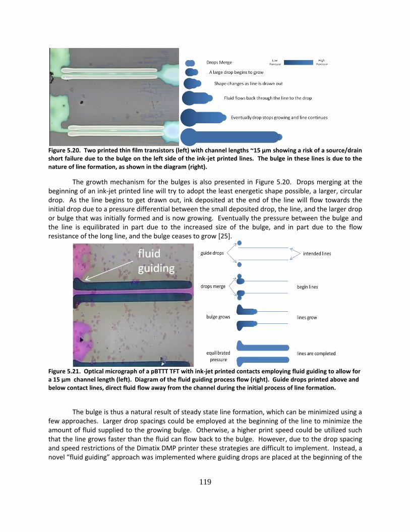
119
Figure 5.20. Two printed thin film transistors (left) with channel lengths ~15 μm showing a risk of a source/drain short failure due to the bulge on the left side of the ink-jet printed lines. The bulge in these lines is due to the nature of line formation, as shown in the diagram (right).
The growth mechanism for the bulges is also presented in Figure 5.20. Drops merging at the beginning of an ink-jet printed line will try to adopt the least energetic shape possible, a larger, circular drop. As the line begins to get drawn out, ink deposited at the end of the line will flow towards the initial drop due to a pressure differential between the small deposited drop, the line, and the larger drop or bulge that was initially formed and is now growing. Eventually the pressure between the bulge and the line is equilibrated in part due to the increased size of the bulge, and in part due to the flow resistance of the long line, and the bulge ceases to grow [25].
Figure 5.21. Optical micrograph of a pBTTT TFT with ink-jet printed contacts employing fluid guiding to allow for a 15 μm channel length (left). Diagram of the fluid guiding process flow (right). Guide drops printed above and below contact lines, direct fluid flow away from the channel during the initial process of line formation.
The bulge is thus a natural result of steady state line formation, which can be minimized using a few approaches. Larger drop spacings could be employed at the beginning of the line to minimize the amount of fluid supplied to the growing bulge. Otherwise, a higher print speed could be utilized such that the line grows faster than the fluid can flow back to the bulge. However, due to the drop spacing and speed restrictions of the Dimatix DMP printer these strategies are difficult to implement. Instead, a novel “fluid guiding” approach was implemented where guiding drops are placed at the beginning of the
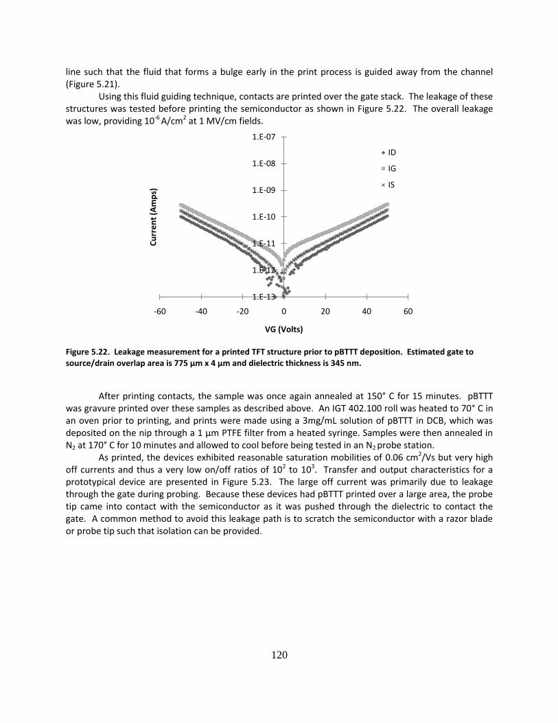
120
line such that the fluid that forms a bulge early in the print process is guided away from the channel (Figure 5.21). Using this fluid guiding technique, contacts are printed over the gate stack. The leakage of these structures was tested before printing the semiconductor as shown in Figure 5.22. The overall leakage was low, providing 10-6 A/cm2 at 1 MV/cm fields.
Figure 5.22. Leakage measurement for a printed TFT structure prior to pBTTT deposition. Estimated gate to source/drain overlap area is 775 μm x 4 μm and dielectric thickness is 345 nm.
After printing contacts, the sample was once again annealed at 150° C for 15 minutes. pBTTT was gravure printed over these samples as described above. An IGT 402.100 roll was heated to 70° C in an oven prior to printing, and prints were made using a 3mg/mL solution of pBTTT in DCB, which was deposited on the nip through a 1 μm PTFE filter from a heated syringe. Samples were then annealed in N2 at 170° C for 10 minutes and allowed to cool before being tested in an N2 probe station. As printed, the devices exhibited reasonable saturation mobilities of 0.06 cm2/Vs but very high off currents and thus a very low on/off ratios of 102 to 103. Transfer and output characteristics for a prototypical device are presented in Figure 5.23. The large off current was primarily due to leakage through the gate during probing. Because these devices had pBTTT printed over a large area, the probe tip came into contact with the semiconductor as it was pushed through the dielectric to contact the gate. A common method to avoid this leakage path is to scratch the semiconductor with a razor blade or probe tip such that isolation can be provided.
1.E-13
1.E-12
1.E-11
1.E-10
1.E-09
1.E-08
1.E-07
-60 -40 -20 0 20 40 60
Cu
rre
nt
(Am
ps)
VG (Volts)
ID
IG
IS
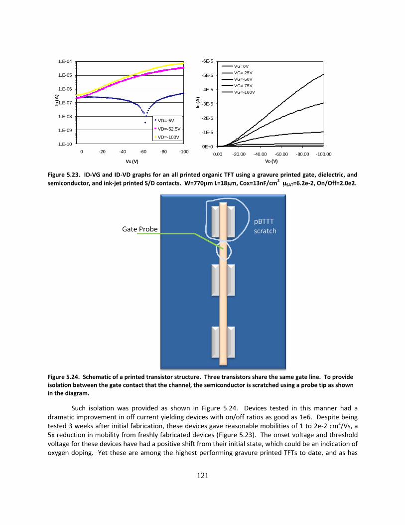
121
Figure 5.23. ID-VG and ID-VD graphs for an all printed organic TFT using a gravure printed gate, dielectric, and
semiconductor, and ink-jet printed S/D contacts. W=770 m L=18 m, Cox=13nF/cm2 SAT=6.2e-2, On/Off=2.0e2.
Figure 5.24. Schematic of a printed transistor structure. Three transistors share the same gate line. To provide isolation between the gate contact that the channel, the semiconductor is scratched using a probe tip as shown in the diagram.
Such isolation was provided as shown in Figure 5.24. Devices tested in this manner had a dramatic improvement in off current yielding devices with on/off ratios as good as 1e6. Despite being tested 3 weeks after initial fabrication, these devices gave reasonable mobilities of 1 to 2e-2 cm2/Vs, a 5x reduction in mobility from freshly fabricated devices (Figure 5.23). The onset voltage and threshold voltage for these devices have had a positive shift from their initial state, which could be an indication of oxygen doping. Yet these are among the highest performing gravure printed TFTs to date, and as has
-6E-5
-5E-5
-4E-5
-3E-5
-2E-5
-1E-5
0E+0
-100.00-80.00-60.00-40.00-20.000.00
ID(A
)
VD (V)
VG=0V
VG=-25V
VG=-50V
VG=-75V
VG=-100V
1.E-10
1.E-09
1.E-08
1.E-07
1.E-06
1.E-05
1.E-04
-100-80-60-40-200
ID(A
)
VG (V)
VD=-5V
VD=-52.5V
VD=-100V
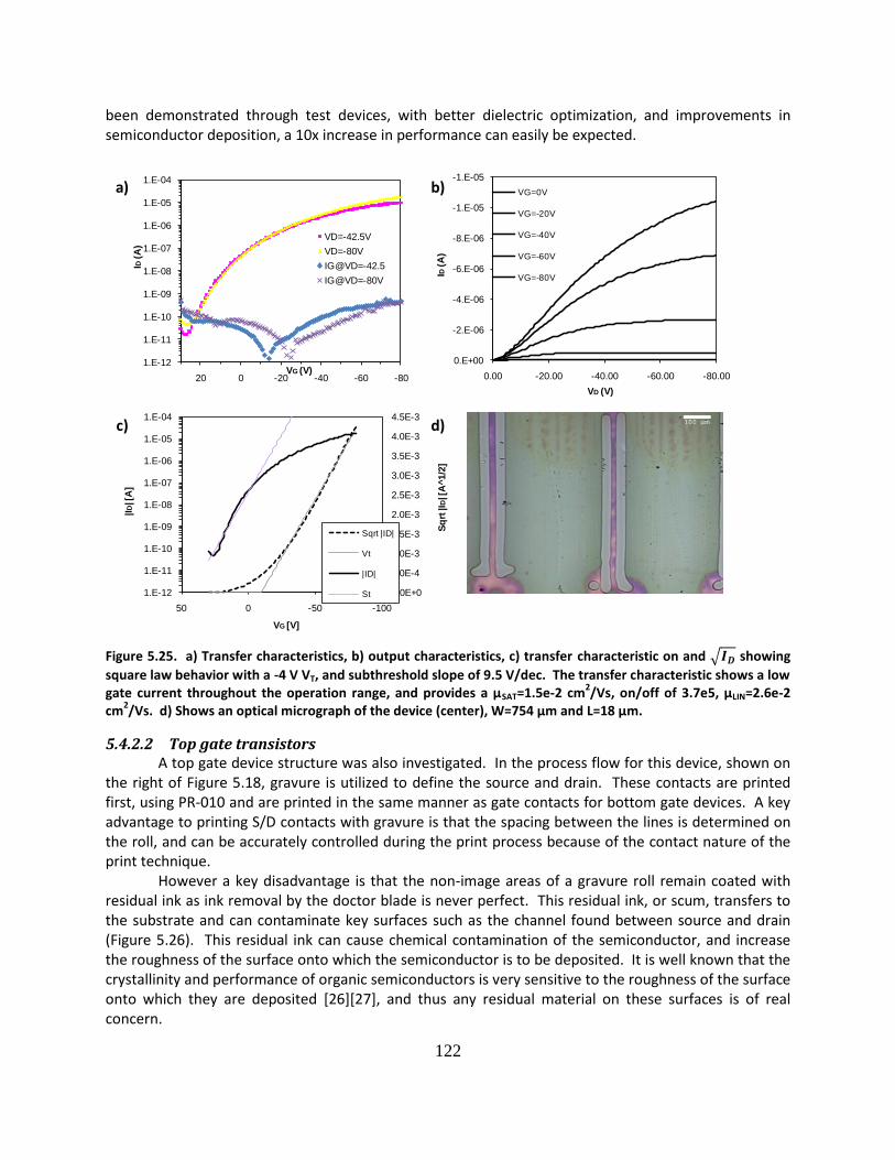
122
been demonstrated through test devices, with better dielectric optimization, and improvements in semiconductor deposition, a 10x increase in performance can easily be expected.
Figure 5.25. a) Transfer characteristics, b) output characteristics, c) transfer characteristic on and showing
square law behavior with a -4 V VT, and subthreshold slope of 9.5 V/dec. The transfer characteristic shows a low gate current throughout the operation range, and provides a μSAT=1.5e-2 cm
2/Vs, on/off of 3.7e5, μLIN=2.6e-2
cm2/Vs. d) Shows an optical micrograph of the device (center), W=754 μm and L=18 μm.
5.4.2.2 Top gate transistors A top gate device structure was also investigated. In the process flow for this device, shown on the right of Figure 5.18, gravure is utilized to define the source and drain. These contacts are printed first, using PR-010 and are printed in the same manner as gate contacts for bottom gate devices. A key advantage to printing S/D contacts with gravure is that the spacing between the lines is determined on the roll, and can be accurately controlled during the print process because of the contact nature of the print technique. However a key disadvantage is that the non-image areas of a gravure roll remain coated with residual ink as ink removal by the doctor blade is never perfect. This residual ink, or scum, transfers to the substrate and can contaminate key surfaces such as the channel found between source and drain (Figure 5.26). This residual ink can cause chemical contamination of the semiconductor, and increase the roughness of the surface onto which the semiconductor is to be deposited. It is well known that the crystallinity and performance of organic semiconductors is very sensitive to the roughness of the surface onto which they are deposited [26][27], and thus any residual material on these surfaces is of real concern.
1.E-12
1.E-11
1.E-10
1.E-09
1.E-08
1.E-07
1.E-06
1.E-05
1.E-04
0.0E+0
5.0E-4
1.0E-3
1.5E-3
2.0E-3
2.5E-3
3.0E-3
3.5E-3
4.0E-3
4.5E-3
-100-50050
|ID| [
A]
Sq
rt |I
D| [
A^1/2
]
VG [V]
Sqrt |ID|
Vt
|ID|
St
1.E-12
1.E-11
1.E-10
1.E-09
1.E-08
1.E-07
1.E-06
1.E-05
1.E-04
-80-60-40-20020
ID(A
)
VG (V)
VD=-42.5V
VD=-80V
IG@VD=-42.5
IG@VD=-80V
-1.E-05
-1.E-05
-8.E-06
-6.E-06
-4.E-06
-2.E-06
0.E+00
-80.00-60.00-40.00-20.000.00
ID(A
)
VD (V)
VG=0V
VG=-20V
VG=-40V
VG=-60V
VG=-80V
a) b)
c) d)
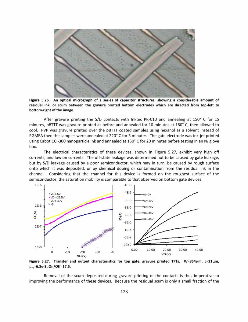
123
Figure 5.26. An optical micrograph of a series of capacitor structures, showing a considerable amount of residual ink, or scum between the gravure printed bottom electrodes which are directed from top-left to bottom-right of the image.
After gravure printing the S/D contacts with Inktec PR-010 and annealing at 150° C for 15 minutes, pBTTT was gravure printed as before and annealed for 10 minutes at 180° C, then allowed to cool. PVP was gravure printed over the pBTTT coated samples using hexanol as a solvent instead of PGMEA then the samples were annealed at 220° C for 5 minutes. The gate electrode was ink-jet printed using Cabot CCI-300 nanoparticle ink and annealed at 150° C for 20 minutes before testing in an N2 glove box. The electrical characteristics of these devices, shown in Figure 5.27, exhibit very high off currents, and low on currents. The off-state leakage was determined not to be caused by gate leakage, but by S/D leakage caused by a poor semiconductor, which may in turn, be caused by rough surface onto which it was deposited, or by chemical doping or contamination from the residual ink in the channel. Considering that the channel for this device is formed on the roughest surface of the semiconductor, the saturation mobility is comparable to that observed on bottom gate devices.
Figure 5.27. Transfer and output characteristics for top gate, gravure printed TFTs. W=854 m, L=21 m,
FE=6.8e-3, On/Off=17.5.
Removal of the scum deposited during gravure printing of the contacts is thus imperative to improving the performance of these devices. Because the residual scum is only a small fraction of the
-4E-6
-4E-6
-3E-6
-3E-6
-2E-6
-2E-6
-1E-6
-5E-7
0E+0
-40.00-30.00-20.00-10.000.00
ID (A
)
VD (V)
VG=0V
VG=-10V
VG=-20V
VG=-30V
VG=-40V
1E-8
1E-7
1E-6
1E-5
-40-30-20-100
ID (A
)
VG (V)
VD=-5V
VD=-22.5V
VD=-40V
IG
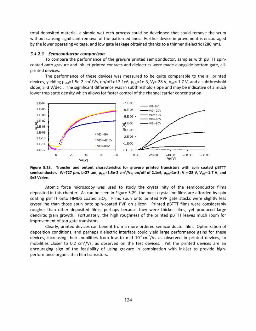
124
total deposited material, a simple wet etch process could be developed that could remove the scum without causing significant removal of the patterned lines. Further device improvement is encouraged by the lower operating voltage, and low gate leakage obtained thanks to a thinner dielectric (280 nm).
5.4.2.3 Semiconductor comparison To compare the performance of the gravure printed semiconductor, samples with pBTTT spin-coated onto gravure and ink-jet printed contacts and dielectrics were made alongside bottom gate, all-printed devices. The performance of these devices was measured to be quite comparable to the all printed devices, yielding μSAT=1.5e-2 cm2/Vs, on/off of 2.1e6, μLIN=1e-3, VT=-28 V, Von=-1.7 V, and a subthreshold slope, S=3 V/dec . The significant difference was in subthreshold slope and may be indicative of a much lower trap state density which allows for faster control of the channel carrier concentration.
Figure 5.28. Transfer and output characteristics for gravure printed transistors with spin coated pBTTT semiconductor. W=727 μm, L=27 μm, μSAT=1.5e-2 cm
2/Vs, on/off of 2.1e6, μLIN=1e-3, VT=-28 V, Von=-1.7 V, and
S=3 V/dec.
Atomic force microscopy was used to study the crystallinity of the semiconductor films deposited in this chapter. As can be seen in Figure 5.29, the most crystalline films are afforded by spin coating pBTTT onto HMDS coated SiO2. Films spun onto printed PVP gate stacks were slightly less crystalline than those spun onto spin-coated PVP on silicon. Printed pBTTT films were considerably rougher than other deposited films, perhaps because they were thicker films, yet produced large dendritic grain growth. Fortunately, the high roughness of the printed pBTTT leaves much room for improvement of top-gate transistors. Clearly, printed devices can benefit from a more ordered semiconductor film. Optimization of deposition conditions, and perhaps dielectric interface could yield large performance gains for these devices, increasing their mobilities from low to mid 10-2 cm2/Vs as observed in printed devices, to mobilities closer to 0.2 cm2/Vs, as observed on the test devices. Yet the printed devices are an encouraging sign of the feasibility of using gravure in combination with ink-jet to provide high-performance organic thin film transistors.
1.E-12
1.E-11
1.E-10
1.E-09
1.E-08
1.E-07
1.E-06
1.E-05
1.E-04
-80-60-40-200
ID[A
]
VG [V]
VD=-5V
VD=-42.5V
VD=-80V
-7.E-06
-6.E-06
-5.E-06
-4.E-06
-3.E-06
-2.E-06
-1.E-06
0.E+00
-80.00-60.00-40.00-20.000.00
ID[A
]
VD [V]
VG=0V
VG=-20V
VG=-40V
VG=-60V
VG=-80V
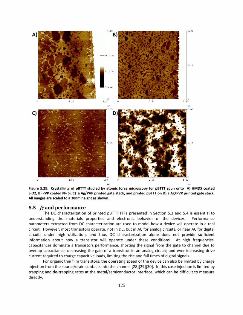
125
Figure 5.29. Crystallinty of pBTTT studied by atomic force microscopy for pBTTT spun onto A) HMDS coated SiO2, B) PVP coated N+ Si, C) a Ag/PVP printed gate stack, and printed pBTTT on D) a Ag/PVP printed gate stack. All images are scaled to a 30nm height as shown.
5.5 fT and performance The DC characterization of printed pBTTT TFTs presented in Section 5.3 and 5.4 is essential to understanding the materials properties and electronic behavior of the devices. Performance parameters extracted from DC characterization are used to model how a device will operate in a real circuit. However, most transistors operate, not in DC, but in AC for analog circuits, or near AC for digital circuits under high utilization, and thus DC characterization alone does not provide sufficient information about how a transistor will operate under these conditions. At high frequencies, capacitances dominate a transistors performance, shorting the signal from the gate to channel due to overlap capacitance, decreasing the gain of a transistor in an analog circuit; and ever increasing drive current required to charge capacitive loads, limiting the rise and fall times of digital signals. For organic thin film transistors, the operating speed of the device can also be limited by charge injection from the source/drain contacts into the channel [28][29][30]. In this case injection is limited by trapping and de-trapping rates at the metal/semiconductor interface, which can be difficult to measure directly.
A) B)
C) D)
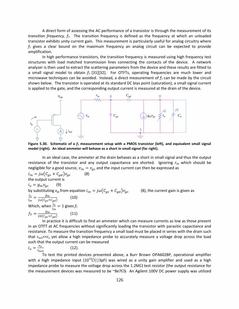
126
A direct form of assessing the AC performance of a transistor is through the measurement of its transition frequency, fT. The transition frequency is defined as the frequency at which an unloaded transistor exhibits unity current gain. This measurement is particularly useful for analog circuitry where fT gives a clear bound on the maximum frequency an analog circuit can be expected to provide amplification. In high performance transistors, the transition frequency is measured using high frequency test structures with load matched transmission lines connecting the contacts of the device. A network analyzer is then used to extract the scattering parameters from the device and these results are fitted to a small signal model to obtain fT [31][32]. For OTFTs, operating frequencies are much lower and microwave techniques can be avoided. Instead, a direct measurement of fT can be made by the circuit shown below. The transistor is operated at its standard DC bias point (saturation), a small signal current is applied to the gate, and the corresponding output current is measured at the drain of the device.
Figure 5.30. Schematic of a fT measurement setup with a PMOS transistor (left), and equivalent small signal model (right). An ideal ammeter will behave as a short in small signal (far right).
In an ideal case, the ammeter at the drain behaves as a short in small signal and thus the output resistance of the transistor and any output capacitance are shorted. Ignoring rin, which should be negligible for a good source, and the input current can then be expressed as
(8)
the output current is (9)
by substituting vgs from equation (8), the current gain is given as
(10)
Which, when gives fT
(11)
In practice it is difficult to find an ammeter which can measure currents as low as those present in an OTFT at AC frequencies without significantly loading the transistor with parasitic capacitance and resistance. To measure the transition frequency a small load must be placed in series with the drain such that rtest<<ro yet allow a high impedance probe to accurately measure a voltage drop across the load such that the output current can be measured
(12).
To test the printed devices presented above, a Burr Brown OPA602BP, operational amplifier
with a high impedance input (1013 ||3pF) was wired as a unity gain amplifier and used as a high
impedance probe to measure the voltage drop across the 1.2M test resistor (the output resistance for
the measurement devices was measured to be ~8e7 An Agilent 100V DC power supply was utilized
vin
rin
Cgs gmvgs ro Co
CgdG D
S
0 0

127
to bias the source and drain to VS=60V, VD=0V. A function generator was used to bias the gate at VG=-4V, and supply a 2V peak-to-peak sinusoidal signal to the gate. The frequency of the input signal was swept while measuring the output voltage at the amplifiers output. This data was then used to calculate iout as described below.
Figure 5.31. Schematic of experimental setup (top) for fT extraction and equivalent small signal circuit (bottom).
Before the measurement, the input capacitance of the transistor was determined by using the measured dielectric capacitance (determined from capacitor measurements with an HP4285 LCR meter), the size of the transistor, and the overlap area of the source and drain contacts (determined using optical microscopy) such that
(13)
where Cins is the dielectric capacitance per unit area in F/cm2 W and L are the transistor width and length, respectively, and LSOL and LDOL are the overlap lengths for the source and drain contacts. The channel capacitance is assumed to be 2/3 of the channel length in saturation as is common practice. Assuming that the overlap lengths are the same for both source and drain, and expressing these lengths as a percentage, , of the channel length, the input capacitance can be written as
(14).
vin
rin
Cgs gmvgs ro Cop
CgdG D
S
rop rtest
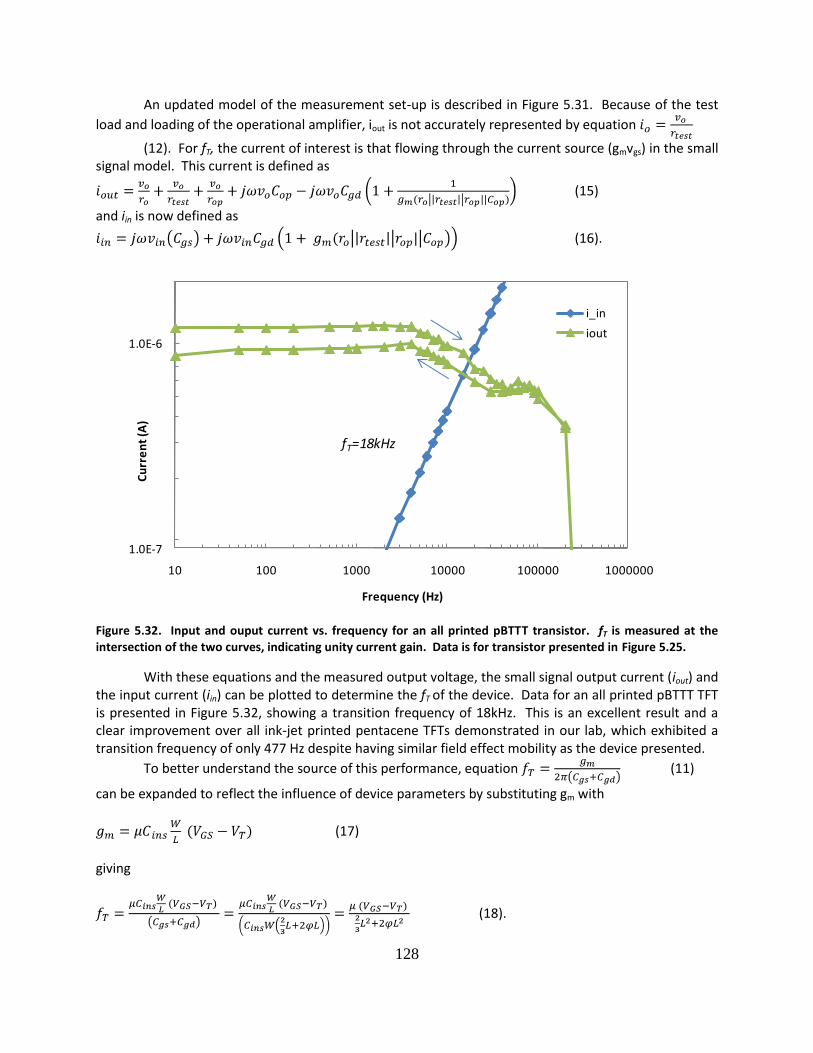
128
An updated model of the measurement set-up is described in Figure 5.31. Because of the test
load and loading of the operational amplifier, iout is not accurately represented by equation
(12). For fT, the current of interest is that flowing through the current source (gmvgs) in the small signal model. This current is defined as
(15)
and iin is now defined as
(16).
Figure 5.32. Input and ouput current vs. frequency for an all printed pBTTT transistor. fT is measured at the intersection of the two curves, indicating unity current gain. Data is for transistor presented in Figure 5.25.
With these equations and the measured output voltage, the small signal output current (iout) and the input current (iin) can be plotted to determine the fT of the device. Data for an all printed pBTTT TFT is presented in Figure 5.32, showing a transition frequency of 18kHz. This is an excellent result and a clear improvement over all ink-jet printed pentacene TFTs demonstrated in our lab, which exhibited a transition frequency of only 477 Hz despite having similar field effect mobility as the device presented.
To better understand the source of this performance, equation (11)
can be expanded to reflect the influence of device parameters by substituting gm with
(17)
giving
(18).
1.0E-7
1.0E-6
10 100 1000 10000 100000 1000000
Cu
rre
nt
(A)
Frequency (Hz)
i_in
iout
fT=18kHz
129
For the device presented here, a transition frequency of 27kHz was calculated with equation
(18), which is in good agreement with the
measured value. It is evident that though clear improvements to fT can be obtained through improvements in field effect mobility, the operation of the device is even more sensitive to its channel length. Herein lays the success of the presented devices. Gravure printed features were scaled down to 20 μm providing devices with channel lengths of 18μm which are a significant improvement over our inkjet printed devices, where despite having a small channel length of 11 μm, had an overlap length on the order of 70 μm. Further, a 10x improvement in mobility can be expected after some dielectric and semiconductor optimization, as has been demonstrated in test devices, leading to devices operating near 200kHz. If the channel length can be further reduced to 10μm, a transition frequency of 900kHz can be expected. We have already measured devices with a 32kHz transition frequency using spin-coated pBTTT on the same printed gate-stack, showing the promise of improved performance. This data is very encouraging as digital circuits can as a rule of thumb, operate at speeds up to ½ fT, and conservatively, 1/10th the transition frequency. As of now, the best results have been obtained by Huebler [33], where 100 μm channel lengths and mobilities of 1.3e-3 cm2/Vs, yield ring oscillators with 3Hz operating frequencies; and Cho[34] where 200 μm channel lengths and good mobilities of up to 2 cm2/Vs provide ring oscillators with only 150 Hz operating frequency. We can thus expect that the operating frequency of digital circuits manufactured with these devices will be significantly better than any other gravure, or roll-to-roll printed transistor to date.
5.6 Conclusion Through a combination of materials and process development, gravure / ink-jet printed organic thin film transistors based on the poly(bi-thieno thiophene) pBTTT semiconductor were demonstrated. These transistors take advantage of the gravure printing processes described in previous chapters for depositing fine metal lines and uniform thin film dielectrics to give a reliable gate stack. They also take advantage of the ability to use hexamethyldisilazane to passivate unreacted hydroxyl groups on the poly-vinyl phenol dielectric, giving a good interface for pBTTT to crystallize; a chemical interaction at metal semiconductor interfaces which gives nanoparticle based silver lines much lower contact resistance to the semiconductor than expected; and a novel ink-jet printing process that can maintain a close and uniform spacing between source and drain contacts to make the devices presented here some of the best gravure printed thin film transistors to date. This is also the first time gravure has been used to print pBTTT, which required a heated solution and gravure roll to maintain stability in solution. Channel lengths of 18 μm have allowed these transistors to operate at very reasonable frequencies as transition frequencies of 18kHz and 32kHz were measured with fully printed devices and devices with spin coated semiconductor, respectively. Significant improvements in operating frequency can still be expected as there is room for a 10x improvement in semiconductor mobility for the printed devices, which has been demonstrated on test devices. At the speeds reported, these transistors could already be used for logic on RFID tags, or as pixel drivers for small displays and near term improvements will make these transistors even more appealing for such applications.
5.7 Works Cited [1] Tessler, Nir, et al., "Charge Transport in Disordered Organic Materials and Its Relevance to Thin-Film Devices: A Tutorial Review." s.l. : Advanced Materials, 2009. pp. 2741-2761. DOI: 10.1002/adma.200803541.
130
[2] Sirringhaus, Henning., "Device Physics of Solution-Processed Organic Field-Effect Transistors." s.l. : Advanced Materials, 2005, Vol. 17, pp. 2411-2425. DOI: 10.1002/adma.200501152. [3] Bao, Zhenan and Locklin, Jason., Organic Field Effect Transistors. Boca Raton : CRC Press, 2007. [4] De Leew, D.M., et al., "Stability of n-type doped conducting polymers and consequences for polymeric microelectronic devices." s.l. : Synthetic Metals, 1997, Vol. 87, pp. 53-59. doi:10.1016/S0379-6779(97)80097-5. [5] McCulloch, Iain, et al., "Liquid-crystalline semiconducting polymers with high charge-carrier mobility." s.l. : Nature Materials, 2006, Vol. 5, pp. 328-333. doi: 10.1038/nmat1612. [6] Yan, He, et al., "A high-mobility electron-transporting polymer for printed transistors." s.l. : Nature, 2009, Vol. 457, p. 679. doi: 10.1038/nature07727. [7] McCulloch, Iain, et al., "Semiconducting Thienothiphene Copolymers: Design, Synthesis, Morphology, and Performance in Thin-Film Organic Transistors." s.l. : Advanced Materials, 2009, Vol. 21, pp. 1091-1109. [8] DeLongchamp, Dean, et al., "High Carrier Mobility Polythiophene Thin Films: Structure Determination by Experiment and Theory." s.l. : Advanced Materials, 2006, Vol. 19, pp. 833-837. DOI: 10.1002/adma.200602651. [9] Merck., UK/MH/05/046 Polymer Process Guidelines. s.l. : Merck KGaA, 2006. [10] Hamadani, B. H., et al., "Undoped polythiophene field-effect transistors with mobility of 1 cm2 V−1 s−1." s.l. : Applied Physics Letters, 2007, Vol. 91, p. 243512. doi:10.1063/1.2824845. [11] Dshoot, Anoop, et al., "Beyond the metal-insulator transition in polymer electrolyte gated polymer field-effect transistors." s.l. : Proceedings of the National Academy of Science, 2006, Issue 32, Vol. 103, pp. 11834-11837. doi: 10.1073/pnas.0605033103. [12] Almanza-Workman, A. Marcia, et al., "Characterizatio of highly hydrophobic coatings deposited onto pre-oxidized silicon from water dispersible organosilanes." s.l. : Thin Solid Films, 2003, Vol. 423, pp. 77-87. [13] Kline, Joseph R., et al., "Significant dependence of morphology and charge carrier mobility on substrate surface chemistry in high performance polythiophene semiconductor films ." s.l. : Applied Physics Letters, 2007, Vol. 90, p. 062117. doi:10.1063/1.2472533. [14] Lucas, Leah, et al., "Combinatorial screening of the effect of temperature on the microstructure and mobility of a high performance polythiophene semiconductor." s.l. : Applied Physics Letters, 2007, Vol. 90, p. 012112. DOI: 10.1063/1.2404934. [15] Lee, Woo I., et al., "Effects of Cooling Rate on the Crystallinity and Mechanical Properties of Thermoplastic Composites." s.l. : Journal of Reinforced Plastics and Composites, 1987, Vol. 6, pp. 2-12. DOI: 10.1177/073168448700600101. [16] Huang, Wen-Kuei, Ko, Chu-Jung and Chen, Fang-Chung., "Organic selective-area patterning method for microlens array fabrication." s.l. : Microelectronic Engineering, 2006, Vol. 83, pp. 1333-1335 . doi:10.1016/j.mee.2006.01.163. [17] Wu, Yialiang, Li, Yuning and Ong, Ben S., "Printed Silver Ohmic Contacts for High-Mobility Organic Thin-Film Transistors." s.l. : Journal of the American Chemical Society, 2006, Vol. 128, pp. 4202-4203. [18] Wu, Yiliang, Li, Yuning and Ong, Ben S., "A Simple and Efficient Approach to a Printable Silver Conductor for Printed Electronics." s.l. : Jounral of the American Chemical Society, 2007, Vol. 129, pp. 1862-1863. [19] Kim, Dongjo, et al., "Heterogeneous Interfacial Properties of Ink-Jet-Printed Silver Nanoparticulate Electrode and Organic Semiconductor." s.l. : Advanced Materials, 2008, Issue 16, Vol. 20, pp. 3084-3089. DOI: 10.1002/adma.200702750.

131
[20] Noh, Yong-Young and Sirringhaus, Hennig., "Ultra-thin polymer gate dielectrics for top-gate polymer field-effect transistors." s.l. : Organic Electronics, 2009, Issue 1, Vol. 10, pp. 174-180. doi:10.1016/j.orgel.2008.10.021. [21] Yamamoto, Koji, et al., "Evaluation of molecular orientation and alignment of poly(3-hexylthiophene) on Au (111) and on poly(4-vinylphenol) surfaces." s.l. : Thin Solid Films, 2008, Vol. 519, pp. 2695-2699. doi:10.1016/j.tsf.2007.04.145. [22] Wallace, D.B. and Hayes, D.J., "Solder Jet Technology Update." s.l. : The International Journal of Microcircuits and Electronic Packaging, 1998, Issue 1, Vol. 21. [23] Kipphan, Helmut., Handbook of Print Media: Technologies and Production Methods. Berlin : Springer-Verlag, 2001. p. 1207. isbn 3-540-67326-1. [24] Henrie, Justin, et al., "Electronic color charts for dielectric films on silicon." s.l. : Optics Express, 2004, Issue 7, Vol. 12, p. 1464. [25] P.C. Duiniveld, J. Fluid Mech., vol. 477 (2003) 175-200., [26] Chabinyc, Michael, et al., "Effects of the surface roughness of plastic-compatible inorganic dielectrics on polymeric thin film transistors." s.l. : Applied Physics Letters, 2007, Vol. 90, p. 233508. doi:10.1063/1.2746955. [27] Jung, Youngsuk, et al., "The Effect of Interfacial Roughness on the Thin Film Morphology and Charge Transport of High-Performance Polythiophenes." s.l. : Advanced Functional Materials, 2008, Vol. 18, pp. 742-750. DOI: 10.1002/adfm.200701089. [28] Majima, Yutaka, et al., "Simultaneous Measurements of Drain-to-Source Current and Carrier Injection Properties of Top-Contact Pentacene Thin-Film Transistors." s.l. : Japanese Journal of Applied Physics, 2007, Vol. 46, pp. 290-293. DOI: 10.1143/JJAP.46.390. [29] Miyadera, Tetsuhiko, et al., "Frequency response analysis of pentacene thin-film transistors with low impedance contact by interface molecular doping." s.l. : Applied physics Letters, 2007, Vol. 91, p. 013512. doi:10.1063/1.2754350. [30] Seshadri, Kannan and Frisbie, C. Dan., "Potentiometry of an operating organic semiconductor field-effect transistor." s.l. : Applied Physics Letters, 2001, Vol. 78, p. 993. doi:10.1063/1.1345805. [31] Lee, Seonghearn., "Direct extraction technique for a small-signal MOSFET equivalent circuit with substrate parameters." s.l. : Microwave and Optical Technology Letters, 2003, Issue 4, Vol. 39, pp. 344-347. DOI: 10.1002/mop.11210. [32] Raskin, J.-P., Gilon, R. and al., et., "Accurate Characterization of Silicon-On-Insulator MOSFETs for the Design of Low-Voltage, Low-Power RF Integrated Circuits." s.l. : Analog Integrated Circuits and Signal Processing, 2000, Issue 2, Vol. 25, pp. 133-155. 10.1023/A:1008380615900. [33] Huelber, A.C., "Ring oscillator fabricated completely by means of mass-printing technologies." s.l. : Organic Electronics, 2007, Vol. 8, pp. 480-486. [34] Cho, Gyoujin., "R2R Printed TFTs and RFID Tags: Demonstration of All Printed 13.56 MHz Operated 1 Bit RFID Tags." Hsinchu, Taiwan : International Symposium on Flexible Electronics and Displays, November 13-14, 2008.
132
6 Outlook and Conclusions This work has demonstrated that the gravure printing technique can be used for the fabrication of electronic components such as metal lines, capacitors, and thin film transistors. The devices presented here are comparable in performance to devices fabricated using more established methods such as ink-jet printing and spin coating. The discoveries made here have not only brought to light the potential of gravure printing as a manufacturing process for electronics, they have uncovered a wide range of possibilities in materials, devices, and processes for printed electronics as will be discussed here. A challenge to making printed electronics a feasible industry that is often insufficiently addressed is the ability to deposit patterned thin films with thickness uniformity, shape uniformity, and roughness comparable to their vacuum deposited counterparts. Chapter 3 described the challenge in finding an ink suitable for depositing thin metal lines that could be used as contacts to thin film devices at plastic compatible temperatures. A wide variety of researchers and manufacturers have developed nanoparticle based inks for this application. Though the rheological properties of these inks have increased dramatically in the last few years, their colloidal stability can still be improved. Even inks formulated with nanoparticles smaller than 10 nm deposit films with aggregated clusters of sizes larger than 150 nm, which is often sufficient to cause a short failure in a thin film device. We demonstrated that organometallic or metal-salt inks can provide a solution to this problem as these inks do not suffer from aggregation effects. However, by their nature, these inks have relatively low metal content by volume, and thus can cause film cracking when deposited in thin films. Further, mass loading is becoming a limiting factor in the scalability of gravure printed features as discussed in Section 3.4 and 3.5. Organometallic lines printed from 30 μm wells are 20 μm wide and only 70 nm thick. Scaling these lines much below 15 μm will make film thicknesses less than 50 nm which can lead to reliability issues. Nanoparticle based inks could resolve this issue as their mass loading can be significantly higher, however their stability at these higher concentrations must be dramatically improved to maintain low roughness films. Another important part of achieving low roughness patterned films is carefully controlling the behavior of the fluids during their deposition and drying. The fluid mechanics of the gravure printing process are still widely unknown. Though Chapter 3 and 4 described in good detail the effects of gravure cell size, shape, and spacing on the printability of inks, there is still much that can be done in terms of understanding how inks fill the gravure cells and how they empty these cells during the printing process. There has been some work on understanding the fluid flow in a gravure cell during printing, and the effects of surface energies on the percentage of ink transferred from the cell to the substrate, most of these studies utilize features that have been scaled up in size dramatically to enable direct observation. By and large these studies give a good foundation on the phenomena at hand, but their results diverge increasingly from reality as feature sizes are scaled well below 20 μm where surface effects and capillary forces become dominant. There is thus ample opportunity to build on the field of printing and microfluidics in general by studying ink transfer from the gravure at a microscopic level. This work would allow for better cell designs that would facilitate reliable ink transfer and smooth, uniform lines. Still, the drying process must be better understood to balance the fluid and material flows during the drying process to avoid coffee ring formation and variance in film thickness. The limits to the resolution and registration capabilities of gravure have been largely technological as demonstrated in Chapter 2. As with photolithography tools for microelectronics, careful precision machine design must be implemented in the development of gravure printing presses. With a sufficient investment gravure printers could have registration capabilities below 1 μm,
133
comparable to photolithography tools for active matrix LCDs. However, a significant hindrance to realizing these registration capabilities have been the plastic substrates utilized to give printed electronics both its low cost and flexibility. Most of these substrates have glass transition temperatures well below 200° C and suffer shrinkage in the 0.1 to 1% range for short thermal cycles to 150° C causing them to have significant dimensional changes during their manufacturing process. Further the elasticity of these materials is quite low, making the handling of these materials a challenge. Truly there is incentive to using more mechanically stable substrates such as metal foils, though perhaps a better solution may be to develop manufacturing processes that are self-assembled or self-aligned such that registration requirements can be relaxed. As discussed in Chapter 4, gravure may not be the most suitable printing process for every layer in an electronic component. Two drawbacks prevent it from being a universally applicable tool. The pressure applied by the gravure roll and specifically thin cell walls, can be exceedingly large on the micro-scale. This pressure can cause embossing and structural damage of soft materials such as polymers, and thus may make gravure unsuitable for printing over multilayered polymeric devices. Second, the inability of the doctor blade to perfectly wipe the non-image area of the gravure roll will dictate that residual material will always be deposited between gravure patterns. These residuals can be detrimental to roughness and impurity sensitive semiconductors, and may prevent gravure from creating patterns in layers that interface with such materials. As shown in Chapter 4 and 5, ink-jet can be leveraged to overcome these problems as it is a non-contact method that can deposit material exclusively where desired. Thus the development and understanding of multiple printing and deposition processes is necessary to achieve the best results and thus technologies such as flexography, lithography, xerography, and screen printing should not be discarded. As shown in Chapter 5, the ability of gravure to produce fine-lines with low roughness and smooth uniform thin films was a key component to making high performance organic thin film transistors. However, the development of these devices required a much larger effort in optimizing the interplay between printing processes, and material interfaces such as those between the semiconductor and dielectric, and semiconductor and metal. As for the field of printed electronics in general, there is a large opportunity for improving device performance, stability, and reliability by optimizing these interfaces. Only until recently has the focus begun to shift away from purely optimizing the semiconductor material for higher mobility, to optimizing the semiconductor interfaces to dielectrics and metal contacts to improve device performance. Here, all-printed devices made with pBTTT as a semiconductor exhibited field effect mobilities of 2x10⁻² cm2/Vs, on/off ratios of 1x10⁶, and maximum operating frequencies of 18 kHz. Yet improvements in semiconductor mobility and contact resistance as demonstrated on test devices could yield printed devices with operating frequencies as high as 900 kHz, making them suitable for a wide variety of applications including RFID tags, and flexible electronic displays. Clearly there is much opportunity in the field of printed electronics. This work has demonstrated that gravure is a good patterning method and that it deserves careful consideration in any manufacturing process for printed devices.