Embed Size (px)
Citation preview
Role of Ion Mass, Implant Dose, and Wafer Temperature on End-of-Range Defects
S. Prussin* TRW Electronic Systems Group, Redondo Beach, California 90278
Kevin S. Jones Department of Materials Science and Engineering, University of Florida, Gainesville, Florida 32611
A B S T R A C T
T h e end-of - range defec ts for Si, P, Ge, a n d As i m p l a n t a t i o n s we re e v a l u a t e d b y t r a n s m i s s i o n e l ec t ron m i c r o s c o p y over a r a n g e of i m p l a n t doses. The re su l t s for P a n d As c losely t r a c k e d t h o s e for Si a n d Ge, respec t ive ly . As t he i m p l a n t dose is inc reased , t he defec t s inc rease s l ight ly for Si a n d P b u t s ign i f ican t ly for t h e h e a v i e r G e a n d As a toms . Fo r i m p l a n t doses j u s t a b o v e t h e cr i t ical va lue for am or ph i za t i on , t he defec t c o n c e n t r a t i o n for t he l i gh t e r Si a n d P a t o m s is a b o u t five t i m e s as g rea t as for t he Ge a n d As. T he a d v a n t a g e of u s i n g low dose Ge p o s t a m o r p h i z a t i o n is d i scussed .
I n a ser ies of p a p e r s (1-6) t he a u t h o r s h a v e r e p o r t e d on a c o n t i n u i n g i nves t i ga t i on in to t he or ig in of de fec t s in ion i m p l a n t e d si l icon. T h e a im of th i s i n v e s t i g a t i o n h a s b e e n to d e v e l o p m e a n s of a p p l y i n g ion i m p l a n t a t i o n to t h e eve r s h r i n k i n g i n t e g r a t e d c i rcui t s t ruc tu res .
F o l l o w i n g i m p l a n t a t i o n it has b e e n f o u n d t h a t a low t em- pe ra tu re , e.g., 550~ r e g r o w t h a n n e a l is e f fec t ive in con- v e r t i n g a m o r p h o u s (~) layers b a c k to s ingle c rys ta l l in i ty as wel l as e lec t r ica l ly ac t iva t ing t he i m p l a n t e d i m p u r i t y a t o m s w i t h i n t he ~ layer. The defects , r e m a i n i n g in t h e re- c rys ta l l ized s t ruc tu re , h a v e b e e n cha rac t e r i zed as fa l l ing in to five ca tegor ies . Of t h e five ca tegor ies of de fec t s de- s c r i bed (2, 4) th i s s t u d y was d i r ec t ed t o w a r d an u n d e r - s t a n d i n g of t he end-of - range or ca tegory II defects . T h e s e are g e n e r a t e d w h e n an a m o r p h o u s layer is p r o d u c e d a n d is f o u n d in t h e c rys ta l l ine ma te r i a l j u s t b e y o n d t he amor - p h o u s - c r y s t a l l i n e (~/C) in terface . By ut i l iz ing p r e a m o r p h i - zat ion, i t is pos s ib l e to avo id some of t he o the r de fec t ca t egor i e s b u t in e a c h case, t h e y are r e p l a c e d b y c a t e g o r y II defec ts .
I m p l a n t doses we re c h o s e n suf f ic ien t ly h i g h so t h a t a n su r face layer was g e n e r a t e d to avo id t he i n t r o d u c t i o n of ca t ego ry I a n d IV defec ts (2), b u t no t so h i g h as to r e su l t in p e a k i m p u r i t y c o n c e n t r a t i o n s in exces s of sol id solubi l i ty . T h e l a t t e r ha s b e e n s h o w n to b e a s soc ia t ed w i t h t he in t ro- d u c t i o n of ca t ego ry V defec ts (4) a n d t h e acce l e r a t ed solu- t i on of ca tegory II defec ts (5-7). Th i s will l imi t t he P im- p l a n t s to t he dose r a n g e of 1 • 1015-2 • 1015 c m -~ a n d t he As doses to t h e r a n g e of 2 • 1014-2 • 1015 c m -2. Fo r Si a n d Ge w i t h u n l i m i t e d misc ib i l i ty in Si, we on ly h a v e l ower l imi t s of 1 • l0 ~5 a n d 2 • 1014 c m -2, respec t ive ly . F o r t h e s e ele- m e n t s we i n v e s t i g a t e d doses u p to 1 • 1026 c m -2.
Experimental Procedure A ser ies of 100 m m d i a m p- type (100) c o m m e r c i a l l y pre-
p a r e d wafe r s w i t h a ca r r i e r c o n c e n t r a t i o n of 2 • 10 z5 c m -3 we re i m p l a n t e d w i th Si a n d P at 50 k e V a n d w i th Ge a n d As at 100 keV. T h e s e i m p l a n t a t i o n s all gave ve ry s imi la r i m p u r i t y d i s t r i b u t i o n s for t he s a m e dose. I m p l a n t a t i o n s we re ca r r i ed ou t w i t h a c o m m e r c i a l ion i m p l a n t e r u s i n g t h e Waycool f ix ture (1), w h i c h c i r cu la ted r o o m t e m p e r a - t u r e f r eon to m o r e eff ic ient ly ex t r ac t t h e h e a t g e n e r a t e d b y t h e ion i m p l a n t a t i o n . Fo r t he Ge, P, a n d As i m p l a n t a t i o n s , t h e b e a m c u r r e n t was m a i n t a i n e d at 280 + 5 ~A. T h e s e c o n d i t i o n s h a v e b e e n s h o w n to r ep re s s d y n a m i c a n n e a l i n g (1). Fo r t he Si an e v e n lower b e a m c u r r e n t was m a i n t a i n e d . Af te r i m p l a n t a t i o n t h e wafers were a n n e a l e d at 550~ for 3h. E x a m i n a t i o n s h o w e d t h a t t he m i l k y a p p e a r a n c e of t he su r face a m o r p h o u s layer h a d d i sappeared . I t w o u l d b e ve ry use fu l to de sc r ibe t he n a t u r e of t he defec ts in t h e as- i m p l a n t e d or in t h e 550~ r e g r o w n mater ia l . Fo r Waycool f ix tur ing , w h e r e d y n a m i c a n n e a l i n g is s u p p r e s s e d , t he dis- c re te defec ts are too smal l to de t ec t b y s t a n d a r d t r a n s m i s -
* Electrochemical Society Active Member.
s ion e l ec t ron m i c r o s c o p y (TEM) e x a m i n a t i o n . We f o u n d t h a t w i t h an add i t i ona l sho r t annea l , i.e., 30 m i n at 90O~ we cou ld o b s e r v e a p a t t e r n of de fec t s w i t h s t a n d a r d TEM. We h a v e u s e d th i s h e a t - t r e a t m e n t p r io r to T E M s p e c i m e n p repa ra t i on .
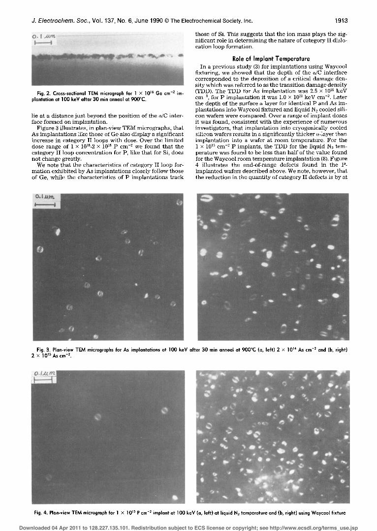
P l a n - v i e w a n d c ross - sec t iona l T E M s p e c i m e n s we re pre- p a r e d a n d e x a m i n e d . P l a n - v i e w m i c r o g r a p h s we re t a k e n u n d e r d a r k field c o n d i t i o n s u s i n g a g040 t w o - b e a m re- f lec t ing c o n d i t i o n a n d are at t h e magn i f i ca t i on l abe l ed in Fig. 3. T h e c ross - sec t iona l T E M m i c r o g r a p h s we re t a k e n u n d e r br ight - f ie ld c o n d i t i o n s u s i n g a g220 t w o - b e a m re- f lec t ing c o n d i t i o n a t t he magn i f i ca t ion l abe l ed in Fig. 2.
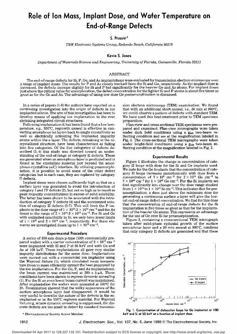
Experimental Results F i g u r e 1 i l lus t ra tes t h e c h a n g e in c o n c e n t r a t i o n of cate-
gory II loops w i th dose for t he Si a n d Ge i m p l a n t s used . We n o t e for t h e Ge i m p l a n t s t h a t t he c o n c e n t r a t i o n of cate- gory II loops inc reases m o n o t o n i c a l l y w i t h dose f rom a c o n c e n t r a t i o n of 7 • 109 c m -2 for 2 • 1024 G e c m -2 to 7 • 101~ c m -2 for 1 • 10 z6 Ge c m -2. F o r t h e Si i m p l a n t s we f ind s ign i f ican t ly less c h a n g e over t he dose r a n g e s t ud i ed f r o m 1 • 1015 to 1 • 1016 Si c m -3. Th i s i nd i ca t e s t h a t for pre- a m o r p h i z a t i o n , a dose j u s t a b o v e t h e m i n i m u m dose for g e n e r a t i n g a c o n t i n u o u s sur face a- layer will g ive t he low- es t end-o f - range defec t concen t r a t i on . We f ind for t h i s dose t h a t t h e c o n c e n t r a t i o n of end-o f - range defec ts for t he Si i m p l a n t a t i o n is five t i m e s as g rea t as t h a t for t he i m p l a n t a - t i on of t he heav ie r Ge a toms. This r e p r e s e n t s a n a d v a n t a g e for t he use of Ge over Si for p r e a m o r p h i z a t i o n .
F i g u r e 2, c o n t a i n i n g a c ross -sec t iona l T E M m i c r o g r a p h t a k e n af te r so l id -phase ep i t ax ia l g r o w t h of t he sur face a m o r p h o u s layer a n d a 30 m i n a n n e a l at 900~ conf i rms t h a t on ly ca tegory II defec ts are g e n e r a t e d a n d t h a t t h e s e
1011
oE
8 ~_ o
1010
9 -o - Ge implant S mpant
1091014 I I I I I t i l l I I I I I I I l l J I I I I I I 1015 1016 1017
Imp;ant Dose, orn-2
Fig. 1. Concentration of dislocation loops for Ge implanted at 100 keV and Si at 50 keV as a function of implant dose.
1912 J. Electrochem. Soc., Vol. 137, No. 6, June 1990 9 The Electrochemical Society, Inc.
Downloaded 04 Apr 2011 to 128.227.135.101. Redistribution subject to ECS license or copyright; see http://www.ecsdl.org/terms_use.jsp
J. Electrochem. Soc., Vol. 137, No. 6, June 1990 9 The Electrochemical Society, Inc. 1913
those of Si. This suggests that the ion mass plays the sig- nif icant role in de t e rmin ing the na ture of ca tegory II dislo- cat ion loop format ion.
Fig. 2. Cross-sectional TEM micrograph for 1 x 10¹⁶ Ge cm -2 im- plantation at 100 keV after 30 mln anneal at 900~
l ie at a d is tance jus t beyond the posi t ion of the a/C inter- face fo rmed on implantat ion.
F igure 3 i l lustrates, in p lan-view T E M micrographs , that As implan ta t ions l ike those of Ge also d isp lay a s ignif icant increase in ca tegory II loops wi th dose. Over the l imi ted dose range of 1 x 101~-2 x 10¹⁵ P cm -2 we found that the ca tegory II loop concent ra t ion for P, l ike that for Si, does not change greatly.
We note that the character is t ics of ca tegory II loop for- ma t ion exh ib i t ed by As implanta t ions closely fol low those of Ge, whi le the character is t ics of P implanta t ions t rack
Role of Implant Temperature In a previous s tudy (3) for implanta t ions us ing Waycool
f ixturing, we showed that the dep th of the a/C interface co r r e sponded to the depos i t ion of a critical damage den- sity wh ich was referred to as the t ransi t ion damage dens i ty (TDD). The TDD for As implan ta t ion was 2.5 x 10²⁰ keV cm -~, for P implan ta t ion it was 1.0 x 10 ~1 keV cm -3. La ter the dep th of the surface ~ layer for ident ical P and As im- planta t ions into Waycool f ixtured and l iquid N2 cooled sili- con wafers were compared . Over a range of implan t doses it was found, consis tent wi th the exper ience of n u m e r o u s invest igators , tha t implan ta t ion into cryogenica l ly cooled si l icon wafers resul ts in a significantly th icker a-layer than implan ta t ion into a wafer at room tempera ture . Fo r the 1 x l0 ts cm -2 P implants , the TDD for the l iquid N2 tem- pera tu re was found to be less than ha l f of the va lue found for the Waycool r o o m tempera tu re implan ta t ion (8). F igure 4 i l lustrates the end-of-range defects found in the P- implan ted wafers descr ibed above. We note, however , that the r educ t ion in the quant i ty of ca tegory II defects is by at
Fig. 3. Plan-view TEM micrographs for As implantations at 100 keV after 30 min anneal at 900~ (a, left) 2 x 10¹⁴ As cm -~ and (b, right) 2 x 101SAscm -2.
Fig. 4. Plan-view TEM micrograph for 1 x 10 ~s P cm -2 implant at 100 keV (a, left) at liquid N2 temperature and (b, right) using Waycool fixture
Downloaded 04 Apr 2011 to 128.227.135.101. Redistribution subject to ECS license or copyright; see http://www.ecsdl.org/terms_use.jsp
1914 J. Electrochem. Soc., Vol. 137, No. 6, June 1990 9 The Electrochemical Society, Inc.
least an order of magnitude. This has been previously noted (9) and is much more than is predicted solely by the reduction of the amount of damage deposited in the crys- talline substrate just beyond the a/C interface.
Discussion The use of Si and Ge implants for pre- and postamorphi-
zation is characterized by the generation of category II de- fects. For light ion implants, the use of Ge preamorphi- zation at doses just exceeding that required to form a surface a-layer is indicated. This would result in the lowest level of category II defects, as has been indicated (10). For room temperature heavy ion implantation at higher doses, our study indicates we could expect a high concentration of category II defects. Our results suggest that the heavy category II defect density resulting from a high dose As implant could be reduced by an order of magnitude by using a low dose Ge postamorphization process.
Manuscript submitted Sept. 20, 1988; revised manu- script received Dec. 4, 1989. This was Paper 176 presented at the Atlanta, GA, Meeting of the Society, May 15-20, 1988.
TRW Electronic Systems Group assisted in meeting the publication costs of this article.
REFERENCES 1. S. Prussin, D. I. Margolese, and R. N. Tauber, J. Appl.
Phys., 54, 2316 (1983). 2. S. Prussin, D.I . Margolese, R. N. Tauber, and W.B.
Hewitt, ibid., 56, 915 (1984). 3. S. Prussin, D. I. Margolese, and R. N. Tauber, ibid., 57,
180 (1985). 4. K. S. Jones, S. Prussin, and E. R. Weber, in "Proceed-
ings of 14th International Conference on Defects in Semiconductors," H.J . von Bardelben, Editor, p. 751, Vol. 10, Materials Science Forum, Trans. Tech. Publications, Aedermansdorf (1986).
5. S. Prussin and K.S. Jones, Nucl. Instrum. Methods Phys. Res., B21, 496 (1987).
6. K. S. Jones, S. Prussin, and E. R. Weber, ibid., B21, 499 (1987).
7. K. S. Jones, S. Prussin, and E. R. Weber, J. Appl. Phys., 62, 4114 (1987).
8. S. Prussin, Abstract 255, p. 369, The Electrochemical Society Extended Abstracts, Vol. 85-1, Toronto, Ont., Canada, May 12-17, 1985.
9. M. Servidori and I. Vecchi, Solid-State Electron, 24, 329 (1981).
10. A. C. Ajmera and G. A. Rozgonyi, Appl. Phys. Lett., 49, 1269 (1986).
Thermally Stable, Low-Leakage Self-Aligned Titanium Silicide Junctions
T. Yoshida, S. Ogawa, and S. Okuda Semiconductor Research Center, Matsushita Electric Industrial Company, Limited, 3-15, Yagumo-Nakamachi,
Moriguchi, Osaka 570, Japan
T. Kouzaki and K. Tsukamoto Matsushita Technoresearch Incorporated, 3-15 Yagumo-Nakamachi, Moriguchi, Osaka 570, Japan
ABSTRACT
A thermally stable, low-leakage-current, self-aligned ti tanium silicide junction has now been fabricated. Ar § sputter etching of Si substrate prior to Ti film deposition followed by two-step rapid thermal annealing in N2 ambient are essential for realization of thermal stability up to 900~ in the ti tanium silicide layer. It is confirmed that the Ar § sputter etching can reduce oxygen contamination at the Ti/Si interface. Consequently the t i tanium silicide layer could be kept extremely flat, with 60 nm thickness with specific resistivity of 19.3 ~l l . cm, even after 900~ 30 min annealing. The junction leakage cur- rent was less than 2.1 nA. cm -2 at reverse bias of 5.0V for n+/p junction.
In sub-micron VLSI fabrication, junctions of both shal- low depth (=< 0.2 ~m) (1) and low sheet resistance are re- quired. TiSi2 is an attractive material for self-aligned sili- cide junction technology (2) for future VLSI fabrication because it has the lowest resistivity among all refractory metal silicides. However, TiSi2 has a high-temperature process limitation. The morphology of TiSi2 films easily degrades (3, 4), and junction leakage currents increase (4) after annealing at temperatures above 900~
Titanium silicide junctions having good electrical prop- erties have been reported; however, thermal treatments after the silicidation were rapid thermal annealing (5, 6) or furnace annealing at 800~176 (7). Recently, many studies have focused on lowering the annealing temperature re- quired for removing defects in source/drain regions of MOSFETs, BPSG melt flow for planarization, and so on. However, we believe that realization of thermally stable silicide junctions up to 900~ for 30-60 min can ease the limitation on processing sub-micron VLSIs. Furthermore, to realize three-dimensional LSIs, which entail fabricating upper-layer LSIs on lower-layer ones, thermal stability up to 900~ is urgently required (8).
In this work, it was confirmed that the thermal stability of TiSi2 films formed on single-crystalline silicon sub- strates by solid-phase reaction was dependent on their for- mation processes. Moreover, we have found a formation
condition in which these silicide junctions maintained ex- cellent electrical properties while bringing about no mor- phological degradation of TiSi2 films, even up to 900~ for 30 min annealing.
Experimental The sample fabrication flow of this work is shown in
Fig. 1. Unpatterened, (100)-oriented, 6-in.-diam p-type Si wafers with a resistivity of 12 gl 9 cm were used for the sub- strates. These wafers were cleaned in H2SO4 + H202 solu- tion. A native oxide layer was removed by dipping in HF solution, just prior to loading into a sputter deposition chamber with a base pressure of 7 • 10 -6 Pa. An Ar § RF sputter etching was performed immediately before Ti film (35 nm) deposition by the dc magnetron sputtering method at room temperature. The Ar § RF sputter etching removed the equivalent of 7 to 9 nm of thermal SIO2. Then Si § implantation was performed at 40 keV with a dose of 5 • 10 is cm -2 for mixing of Ti/Si-substrate interfaces. After cleaning in HNO3 at room temperature, a self-aligned silicidation was performed by a two-step rapid thermal an- nealing (RTA) using A.G. Associates Heatpulse Model 2106 halogen-lamp annealer. A first silicidation was done at 625~ for 60s in N2 ambient (first step RTA), and then the ti- tanium nitride layer formed at the surface was removed se- lectively by an etchant of H2SO4 + H202, leaving the ti-
Downloaded 04 Apr 2011 to 128.227.135.101. Redistribution subject to ECS license or copyright; see http://www.ecsdl.org/terms_use.jsp