Embed Size (px)
Citation preview
Rojas, Felix and Cardenas, Roberto and Kennel, Ralph and Clare, Jon C. and Diaz, Matias (2016) A simplified space-vector modulation algorithm for four-leg NPC converters. IEEE Transactions on Power Electronics, 32 (11). pp. 8371-8380. ISSN 1941-0107
Access from the University of Nottingham repository: http://eprints.nottingham.ac.uk/47231/1/A%20Simplified%20Space%20Vector%20Modulation%20Algorithm.pdf
Copyright and reuse:
The Nottingham ePrints service makes this work by researchers of the University of Nottingham available open access under the following conditions.
This article is made available under the University of Nottingham End User licence and may be reused according to the conditions of the licence. For more details see: http://eprints.nottingham.ac.uk/end_user_agreement.pdf
A note on versions:
The version presented here may differ from the published version or from the version of record. If you wish to cite this item you are advised to consult the publisher’s version. Please see the repository url above for details on accessing the published version and note that access may require a subscription.
For more information, please contact [email protected]

1
A Simplified Space Vector Modulation Algorithmfor Four-Leg NPC Converters
Felix Rojas, Roberto Cardenas, IEEE Senior Member, Ralph Kennel, IEEE Senior Member, Jon Clare, IEEESenior Member, and Matias Diaz, IEEE Student Member
Abstract—To interface generation sources and loads to four-wire distribution networks is important to use power convertersand modulation methods which provide high performance, flexi-bility and reliability. To achieve these goals, this paper proposesa simple and efficient Space Vector Modulation (SVM) algorithmin αβγ coordinates for Neutral Point Clamped (NPC) converters.The proposed SVM method reduces a three-dimensional (αβγ)search of the modulating vectors into a simple two-dimensional(αβ) problem. Moreover, the algorithm provides full utilisationof the dc-link voltage, full utilisation of the redundant vectorsand it can be applied to any other four-leg converter topology.The proposed SVM has been successfully validated using a6kW three-level four-leg NPC converter, achieving control overthe voltages of the dc-link capacitors and simple definition ofswitching pattern for shaping frequency spectrum.
Index Terms—NPC converters, four-leg converters, Space vec-tor Modulation (SVM), Distributed Power Generation Systems(DPGS), Unbalanced Distribution Systems.
I. INTRODUCTION
DUring the last decades, the Neutral Point Clamped (NPC)converter has played an important role in the integra-
tion of renewable energy sources into the electrical system[1]. NPC- based commercial solutions to interface relativelylarge Wind Energy Conversion Systems to medium voltagetransmission lines are already available in the market [2]–[4]. The utilisation of NPC converters in micro-grids and lowvoltage distribution systems has also been reported [5]. Inthis sort of applications the advantages of the NPC convertersare mainly the high effective switching frequency, allowing anoticeable reduction in the filter size, and the high overallefficiency which is important in some applications, e.g tointerface photo voltaic (PV) energy to domiciliary and powerplants applications [4], [6].
In four-leg low voltage distribution networks, a path forthe circulation of zero sequence current is mandatory for
This work was supported by BMBF Germany Grant Nr. 01DN13018 andFondecyt Chile, Grant Nr. 1140337. The support of the Basal Project FB0008is also kindly acknowledged.
Felix Rojas is with the Electrical Engineering Department, University ofSantiago of Chile, Avenida Ecuador N 3519, Estacion Central, Santiago ([email protected]).
Ralph Kennel is with the Institute for Electrical Drive Systems and PowerElectronics, Technical University of Munich, Arcisstr. 21, 80333, Munich(email [email protected]).
Roberto Cardenas and Matıas Dıaz are with the Electrical EngineeringDepartment, University of Chile, Avenida Tupper 2007, Santiago, Chile ([email protected], [email protected]).
Jon Clare is with the Department of Electrical and Electronic Engineering,University of Nottingham, Nottingham University Park, Nottingham, NG7,2RD, (email [email protected]).
the connection of linear and non-linear single-phase loads[7], [8]. There are several well- established methods reportedin the literature to provide a fourth wire for the circulationof zero sequence current. For instance, a (bulky) delta-wyetransformer for providing a neutral wire from the neutral pointof the secondary side of the transformer. Another solution is toprovide a fourth wire connection using the middle point of asplit dc-link capacitor. However, as reported in [8], this methodusually produces a less efficient utilisation of the dc-linkvoltage and higher ripple in the dc-link capacitors. Probablythe best arrangement to provide a path for the circulation ofzero sequence currents is adding an extra leg in the powerconverter [7]. This solution provides control over the zerosequence signals and provides full utilization of the dc-linkvoltage.
The application of two-level four-leg converters [9], [10],and four-leg matrix converters [11]–[13] to four-wire dis-tribution networks, have been extensively reported and areconsidered good alternatives for connecting Distributed PowerGeneration Systems (DPGs) to low voltage grids. However,when high efficiency is desirable combined with high effectiveswitching frequency (for small-size power filter), four-legNPC converters are better alternatives [14]. Moreover, thecapability of synthesising high fundamental frequencies withlow distortion is also desirable in some four-wire applications,as for instance in the aerospace industry where fundamentalsignals above 400 Hz are required [12], [15]. Considering allthe aforementioned issues, four-leg multilevel converters, suchas the four-leg NPC converter shown in Fig. 1, are attractivesolutions [14], [16], [17].
iaibicif
S2c
S1c
S2b
S1b
S2a
S1a
S1c
S2c
S1b
S2b
S1a
S2a
iP
iC1
C1vC1 (t)
vC2(t) C2
iC2
iN
ziz
S1f
S2f
S2f
S1f
abcf
2vdc
+
-
P
N
Fig. 1. Electrical diagram for a four-leg Neutral-Point-Clamped Inverter
To control four-leg NPC converters, different modulationapproaches have been proposed in the literature. For in-
2
stance, in [14] non-linear controllers, such as Finite-Set ModelPredictive Control (FS-MPC), are proposed. Unfortunately,the variability of the switching frequency is an importantdrawback of this approach. The use of Carrier-Based PulseWidth Modulation (PWM) applied independently to each legof the converter has been addressed in [18]. These methodsare easy to implement. However, they do not allow selectionand building of vector switching patterns, which are usuallyrequired to modify the shape of the harmonic spectrum or toreduce the switching power losses. Furthermore, carrier-basedPWM methods do not allow the use of vector redundanciesto control the voltage imbalance in the NPC dc-link capac-itors, important issue when operation with a low switchingfrequency is required [19], [20].
A three-dimensional algorithm in abc coordinates have beenproposed in [21]. This algorithm makes full utilization ofthe dc-link voltage and can modulate a reference vector witha simple and fast algorithm. However, the representation inabc coordinates inherently limits the potential of this SVMmethod, as the zero sequence can not be directly controlled.For instance overmodulation algorithms, as that proposed in[22], [23]; balancing of the capacitor voltages; and evenharmonic elimination, [24], [25] are complex to implementwhen SVMs based on abc coordinates are applied to NPCconverters. On the other hand, all these features are simple toimplement with the SVM proposed in this work.
In this paper, a simplified and low-computational-burdenSVM algorithm for three-level four-leg NPC converters is pre-sented. The simplicity of the method is based on transforminga three-dimensional search of the modulating vectors, intoa much simpler 2-dimensional (αβ) problem. Moreover, theproposed SVM can be extended to any number of levels forany four-leg power converter topology.
The rest of this paper is organized as follows: In Section IIthe proposed modulation algorithm is discussed. In Section IIIexperimental results, obtained with a 6kW lab prototype, arediscussed and fully analysed. In Section IV an appraisal ofthe proposed method is introduced. Finally, in the appendixthe look-up tables summarising the switching states of theconverter are presented.
II. THREE DIMENSIONAL SPACE VECTOR MODULATIONFOR A FOUR-LEG NPC INVERTER
Any space vector modulation strategy is based on thevoltage-second average, where a set of voltage vectors, whichrepresent the switching states of the converter, are used toaverage a reference value over one sampling time [23]. TheClarke transformation presented in (1) is used to obtain thevectorial representation of the switching combinations of theconverter in an αβγ space.
T αβγabc =
2
3
1 −1/2 −1/2
0√
3/2 −√
3/21/2 1/2 1/2
(1)
After the vector representation of the switching combina-tions is obtained, there are mainly three steps required to fulfilthe modulation, these are described as follows: 1) To select thefour-vector (tetrahedron) required to synthesise the reference
αβ
γ
2
1
0
-1
-21.5 1
0-1.5
1.51
0
-1.5
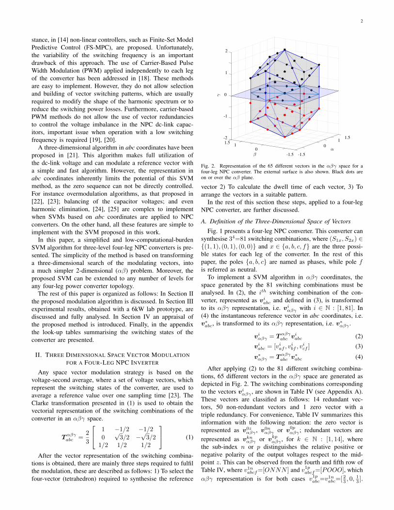
Fig. 2. Representation of the 65 different vectors in the αβγ space for afour-leg NPC converter. The external surface is also shown. Black dots areon or over the αβ plane.
vector 2) To calculate the dwell time of each vector, 3) Toarrange the vectors in a suitable pattern.
In the rest of this section these steps, applied to a four-legNPC converter, are further discussed.
A. Definition of the Three-Dimensional Space of Vectors
Fig. 1 presents a four-leg NPC converter. This converter cansynthesise 34=81 switching combinations, where (S1x, S2x) ∈(1, 1), (0, 1), (0, 0) and x ∈ a, b, c, f are the three possi-ble states for each leg of the converter. In the rest of thispaper, the poles a, b, c are named as phases, while pole fis referred as neutral.
To implement a SVM algorithm in αβγ coordinates, thespace generated by the 81 switching combinations must beanalysed. In (2), the ith switching combination of the con-verter, represented as viabc and defined in (3), is transformedto its αβγ representation, i.e. viαβγ with i ∈ N : [1, 81]. In(4) the instantaneous reference vector in abc coordinates, i.e.v∗abc, is transformed to its αβγ representation, i.e. v∗αβγ .
viαβγ = T αβγabc viabc (2)
viabc = [viaf , vibf , v
icf ] (3)
v∗αβγ = T αβγabc v∗abc (4)
After applying (2) to the 81 different switching combina-tions, 65 different vectors in the αβγ space are generated asdepicted in Fig. 2. The switching combinations correspondingto the vectors viαβγ , are shown in Table IV (see Appendix A).These vectors are classified as follows: 14 redundant vec-tors, 50 non-redundant vectors and 1 zero vector with atriple redundancy. For convenience, Table IV summarizes thisinformation with the following notation: the zero vector isrepresented as v0z
αβγ , v0nαβγ or v0p
αβγ ; redundant vectors arerepresented as vknαβγ or vkpαβγ , for k ∈ N : [1, 14], wherethe sub-index n or p distinguishes the relative positive ornegative polarity of the output voltages respect to the mid-point z. This can be observed from the fourth and fifth row ofTable IV, where v1nabcf=[ONNN ] and v1pabcf=[POOO], whichαβγ representation is for both cases v1pabc=v
1nabc=[ 23 , 0,
13 ].
3
Finally, vkαβγ for k ∈ N : [15, 50] represent the non-redundantvectors.
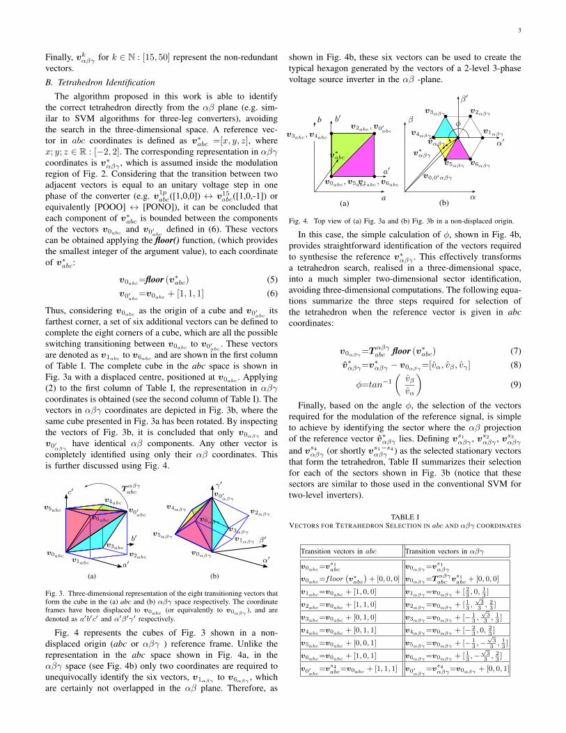
B. Tetrahedron Identification
The algorithm proposed in this work is able to identifythe correct tetrahedron directly from the αβ plane (e.g. sim-ilar to SVM algorithms for three-leg converters), avoidingthe search in the three-dimensional space. A reference vec-tor in abc coordinates is defined as v∗abc =[x, y, z], wherex; y; z ∈ R : [−2, 2]. The corresponding representation in αβγcoordinates is v∗αβγ , which is assumed inside the modulationregion of Fig. 2. Considering that the transition between twoadjacent vectors is equal to an unitary voltage step in onephase of the converter (e.g. v1p
abc([1,0,0]) ↔ v15abc([1,0,-1]) or
equivalently [POOO] ↔ [PONO]), it can be concluded thateach component of v∗abc is bounded between the componentsof the vectors v0abc and v0′abc
defined in (6). These vectorscan be obtained applying the floor() function, (which providesthe smallest integer of the argument value), to each coordinateof v∗abc:
v0abc=floor (v∗abc) (5)v0′abc
=v0abc + [1, 1, 1] (6)
Thus, considering v0abc as the origin of a cube and v0′abcits
farthest corner, a set of six additional vectors can be defined tocomplete the eight corners of a cube, which are all the possibleswitching transitioning between v0abc to v0′abc
. These vectorsare denoted as v1abc to v6abc and are shown in the first columnof Table I. The complete cube in the abc space is shown inFig. 3a with a displaced centre, positioned at v0abc . Applying(2) to the first column of Table I, the representation in αβγcoordinates is obtained (see the second column of Table I). Thevectors in αβγ coordinates are depicted in Fig. 3b, where thesame cube presented in Fig. 3a has been rotated. By inspectingthe vectors of Fig. 3b, it is concluded that only v0αβγ andv0′αβγ
have identical αβ components. Any other vector iscompletely identified using only their αβ coordinates. Thisis further discussed using Fig. 4.
v0abc
v5abc
v1abc
v2abc
v3abc
v0′abc
v4abc
v6abc
v0′αβγ
v0αβγ
v5αβγ
v6αβγ
v4αβγ
v3αβγ
v2αβγ
v1αβγ
Tαβγabc
(a) (b)
a′
b′
c′
α′
β′
γ′
Fig. 3. Three-dimensional representation of the eight transitioning vectors thatform the cube in the (a) abc and (b) αβγ space respectively. The coordinateframes have been displaced to v0abc (or equivalently to v0αβγ ), and aredenoted as a′b′c′ and α′β′γ′ respectively.
Fig. 4 represents the cubes of Fig. 3 shown in a non-displaced origin (abc or αβγ ) reference frame. Unlike therepresentation in the abc space shown in Fig. 4a, in theαβγ space (see Fig. 4b) only two coordinates are required tounequivocally identify the six vectors, v1αβγ to v6αβγ , whichare certainly not overlapped in the αβ plane. Therefore, as
shown in Fig. 4b, these six vectors can be used to create thetypical hexagon generated by the vectors of a 2-level 3-phasevoltage source inverter in the αβ -plane.
v0abc ,v5abcv1abc ,v6abc
v2abc ,v0′abc
v∗abc
b
a
v2αβγ
v1αβγ
v6αβγ
v3αβγ
v4αβγ
v5αβγ
β
α
v∗αβγ
v0,0′αβγ
v∗αβγ
φ
(a) (b)
α′
β′
a′
b′
v3abc ,v4abc
Fig. 4. Top view of (a) Fig. 3a and (b) Fig. 3b in a non-displaced origin.
In this case, the simple calculation of φ, shown in Fig. 4b,provides straightforward identification of the vectors requiredto synthesise the reference v∗αβγ . This effectively transformsa tetrahedron search, realised in a three-dimensional space,into a much simpler two-dimensional sector identification,avoiding three-dimensional computations. The following equa-tions summarize the three steps required for selection ofthe tetrahedron when the reference vector is given in abccoordinates:
v0αβγ=T αβγabc floor (v∗abc) (7)
v∗αβγ=v∗αβγ − v0αβγ=[vα, vβ , vγ ] (8)
φ=tan−1(vβvα
)(9)
Finally, based on the angle φ, the selection of the vectorsrequired for the modulation of the reference signal, is simpleto achieve by identifying the sector where the αβ projectionof the reference vector v∗αβγ lies. Defining vs1αβγ , vs2αβγ , vs3αβγand vs4αβγ (or shortly vs1−s4αβγ ) as the selected stationary vectorsthat form the tetrahedron, Table II summarizes their selectionfor each of the sectors shown in Fig. 3b (notice that thesesectors are similar to those used in the conventional SVM fortwo-level inverters).
TABLE IVECTORS FOR TETRAHEDRON SELECTION IN abc AND αβγ COORDINATES
Transition vectors in abc Transition vectors in αβγ
v0abc=vs1abc v0αβγ=vs1αβγ
v0abc=floor(v∗abc
)+ [0, 0, 0] v0αβγ=Tαβγabc vs1abc + [0, 0, 0]
v1abc=v0abc + [1, 0, 0] v1αβγ=v0αβγ + [ 23, 0, 1
3]
v2abc=v0abc + [1, 1, 0] v2αβγ=v0αβγ + [ 13,√
33, 23
]
v3abc=v0abc + [0, 1, 0] v3αβγ=v0αβγ + [− 13,√
33, 13
]
v4abc=v0abc + [0, 1, 1] v4αβγ=v0αβγ + [− 23, 0, 2
3]
v5abc=v0abc + [0, 0, 1] v5αβγ=v0αβγ + [− 13,−√
33, 13
]
v6abc=v0abc + [1, 0, 1] v6αβγ=v0αβγ + [ 13,−√
33, 23
]
v0′abc
=vs4abc=v0abc + [1, 1, 1] v0′αβγ
=vs4αβγ=v0αβγ + [0, 0, 1]
4
TABLE IISELECTED SEQUENCE OF VECTORS
φ vs1−s4αβγ
Sector 1: φ ∈[0, π
3
[v0αβγ − v1αβγ − v2αβγ − v0′αβγ
Sector 2: φ ∈[π3, 2π
3
[v0αβγ − v2αβγ − v3αβγ − v0′αβγ
Sector 3: φ ∈[2π3, π
[v0αβγ − v3αβγ − v4αβγ − v0′αβγ
Sector 4: φ ∈[π, 4π
3
[v0αβγ − v4αβγ − v5αβγ − v0′αβγ
Sector 5: φ ∈[4π3, 5π
3
[v0αβγ − v5αβγ − v6αβγ − v0′αβγ
Sector 6: φ ∈[5π3, 2π
[v0αβγ − v6αβγ − v1αβγ − v0′αβγ
Using the proposed algorithm, only the calculation of v0αβγ
is required for the identification of the four vectors used tosynthesise the reference. As shown on Table I, all the vectorsthat form the hexagon in the αβ plane around v0αβγ (v1αβγ
to v6αβγ) are obtained just by adding a constant term to v0αβγ
(see second column of Table I).
C. Switching Sequence
In order to minimise the number of devices switchingin each modulation period (minimum switching transitionprinciple [7]), the vectors have to be applied in a pre-definedsequence. In this work the four selected vectors are arrangedusing always v0αβγ and v0′αβγ
as the first and last vectorsof the sequence respectively (or vice-versa). For the proposedSVM algorithm the modulation sequence is similar to thatused in a three-leg converter and this is shown in the secondcolumn of Table II.
In order to reduce the total harmonic distortion of thegenerated waveform, a mirror pattern can be implemented.Thereby, the sequence is symmetrically repeated during halfof the total sampling time Ts. For instance, for sector 1 theproposed sequence is:
Sector1 : v0αβγ v1αβγ v2αβγ v0′αβγv2αβγ v1αβγ v0αβγ
(10)
Notice that other switching sequences can be implementedusing the proposed methodology, e.g. discontinuous modula-tion for minimizing the switching frequency of the devices,other modulation patterns to reduce the output distortion [7],etc.
D. Dwell time Calculation
Once the four stationary vectors, vs1αβγ to vs4αβγ , are obtainedusing (9) and Table II, their dwell times must be calculated.Defining d1, d2, d3 and d4 as the dwell times for each of theselected vectors vs1−s4αβγ , and Ts as the sampling time, theirnormalized values can be obtained from: d2
d3d4
= Dn
v∗α
v∗β
v∗γ
(11)
d1 = 1− d2 − d3 − d4 (12)
where, from (8) the vector v∗αβγ is equivalent to referring thevector v∗αβγ to a new αβγ plane, where the origin is located atv0αβγ (i.e. α′β′γ′ from Fig. 4b). Using this displaced origin,the vectors v1αβγ to v6αβγ will be placed always in the sameposition, forming the typical hexagon in the αβ plane of atwo-level VSI (see second column of Table II). By that, sixdifferent 3x3 matrices Dn can be defined to calculate the dwelltimes in all the space. This matrices take six different valuesdepending on the sector defined by the angle φ (see Fig. 4b).Thereby, based on the second column of Table I, Dn can beexpressed for each interval as φ ∈
[(n−1)π
3 , nπ3
[:
D1 =
32 -
√32 0
0√
3 0
- 12 -√32 1
D2 =
- 32√32 0
32
√32 0
- 12 -√32 1
D3 =
0√
3 0
- 32 -√32 0
1 0 1
D4 =
0 -√
3 0
- 32√32 0
1 0 1
D5 =
- 32 -√32 0
32 -
√32 0
- 12√32 1
D6 =
32
√32 0
0 -√
3 0
- 12√32 1
(13)
The diagram shown in Fig. 5 summarises the proposedmethodology to implement a SVM algorithm in the αβγcoordinate frame for a four-leg NPC converter. As depictedin this figure, after only two steps the required vectors vs1−s4αβγ
are identified. Moreover, the calculation of their correspondingdwell-times, d1 to d4, is simple to realise using the vector v∗αβγ(see (11)-(13)).
For a real-time implementation of the proposed SVM algo-rithm, Table IV is not strictly required. However, this table isuseful for other tasks, for instance to detect overmodulation,(see Fig. 2). Moreover, to add look-up tables with the infor-mation presented in Table IV represents a negligible use ofmemory space in any of the Digital Signal Processors (DSPs)currently used for power electronics applications.
Although in this work the proposed methodology is pre-sented and analysed for a four-leg NPC converter, the flexibil-ity of this algorithm allows a straightforward implementationin any four-wire topology.
E. Capacitors Voltage BalanceOnce the four stationary vectors that enclose the reference
have been selected and their dwell-times have been calculated.The redundant vector with the largest dwell-time can be usedto actively balance the voltages on the dc-link capacitorsvC1(t) and vC2(t) of Fig. 1. For this, one dwell-time hasto be subdivided into to two sub-dwell-times, one for eachredundancy of the redundant vector. Assuming that vs4αβγ isthe redundant vector, the average current through the neutralpoint generated by the converter in one sampling time can becalculated as [14]:
i∗z =d1 · iz1(vs1αβγ) + d2 · iz2(vs2αβγ) + d3 · iz3(vs3αβγ)+ (14)
+ λ · d4 · iz4(vs4pαβγ)− (1− λ) · d4 · iz4(vs4nαβγ)

5
((7),(8), (9))
v∗αβγ
Reference given by external Controller
Calculation of v0αβγ ; v∗αβγ ;φ:
vs4αβγ=v0αβγ + [0, 0, 1]vs1αβγ=v0αβγ
φ ∈[0, π3
[φ ∈
[π3 ,
2π3
[φ ∈
[2π3 , π
[φ ∈
[π, 4π3
[φ ∈
[4π3 ,
5π3
[φ ∈
[5π3 , 2π
[
vs2αβγ=v1αβγ
vs3αβγ=v2αβγ
dᵀ=D1 v∗ᵀαβγ
vs2αβγ=v3αβγ
vs3αβγ=v2αβγ
dᵀ=D2 v∗ᵀαβγ
vs2αβγ=v3αβγ
vs3αβγ=v4αβγ
dᵀ=D3 v∗ᵀαβγ
vs2αβγ=v5αβγ
vs3αβγ=v4αβγ
dᵀ=D4 v∗ᵀαβγ
vs2αβγ=v5αβγ
vs3αβγ=v6αβγ
dᵀ=D5 ∗vᵀαβγ
vs2αβγ=v1αβγ
vs3αβγ=v6αβγ
dᵀ=D6 v∗ᵀαβγ
(Sector 1) (Sector 2) (Sector 3) (Sector 4) (Sector 5) (Sector 6)
Fig. 5. General diagram for a three-dimensional SVM. dᵀ denotes the transpose of the vector d= [d2, d3, d4]. The dwell time d1 is obtained as d1=1 −d2 − d3 − d4; ∀ φ.
where vs1−s4αβγ are the selected stationary vectors for mod-ulating a reference value, d1, d2, d3 and d4 are the dwell-times calculated in (11), iz1 , iz2 , iz3 and iz4 are the currentsthrough the neutral-point (z of Fig. 1) generated by each ofthe vectors vs1−s4αβγ , i∗z is the required reference current, givenby an external PI controller, to balance the voltages vC1 andvc2 and λ is the variable to be calculated which provides theportion of the positive and negative redundancy used in theredundant vector. Thereby, knowing λ, the sub-dwell time aresimply obtained from (14) as:
d4p =λ · d4 (15)d4n =(1− λ) · d4 (16)
III. EXPERIMENTAL RESULTS
The experimental rig used to validate the proposed SVMalgorithm is depicted in Fig. 6. The control platform isbased on a Pentium-System board (2Gb RAM host PC witha 3.2GHz Pentium processor running the RTAI Arch-Linuxoperating system) and a FPGA board. The FPGA boardhandles the signals measured by the A/D converters; imple-ments over-voltage and over-current protection; implementsthe commutation dead time; and handles the control signalsfor the IGBTs switches which are transmitted to the powerconverter using optical fibres. The four-leg NPC converteris based on the semiconductor module Microsemi IGBT-APTGL60TL120T3G, 60A and 1200V . The experimentaldata has been acquired using a Textronix DPO 2024 DigitalPhosphor Osciloscope, 200MHz, 1GS/s.
Notice that the execution time for the proposed simplifiedSVM algorithm is less than 20 µ sec.
A. Modulation of Balanced and Unbalanced VoltagesIn order to validate the performance of the proposed SVM
algorithm, two criteria are considered. First, the converter
Control Platform
Power Electronics Interface
Oscilloscopes
Fig. 6. Complete view of a 6kW experimental rig for a four-leg NPCconverter.
must be able to modulate each of the harmonic componentspresent at the reference waveform. Secondly, the modulatedwaveforms must fulfil the minimum switching transition prin-ciple, generating a pulse pattern which reduces the harmonicdistortion and switching losses. The results discussed in thissection have been obtained applying switching patterns similarto that of (10). Additionally, the parameters of Table III havebeen used.
TABLE IIIGENERAL PARAMETERS OF THE IMPLEMENTED SYSTEMS
Parameter Value Parameter ValueC1 3300 uF fs 6kHzC2 3300 uF 2Vdc 270 V
Firstly, the SVM algorithm is tested with a set of sinusoidal,
6
balanced and symmetric references. These references possesan amplitude equal to 95 % of the maximum value achievableby the modulation in the linear region.
v∗af=270√
30.95 cos(100πt) (17)
v∗bf=270√
30.95 cos(100πt− 2π
3) (18)
v∗cf=270√
30.95 cos(100πt+
2π
3) (19)
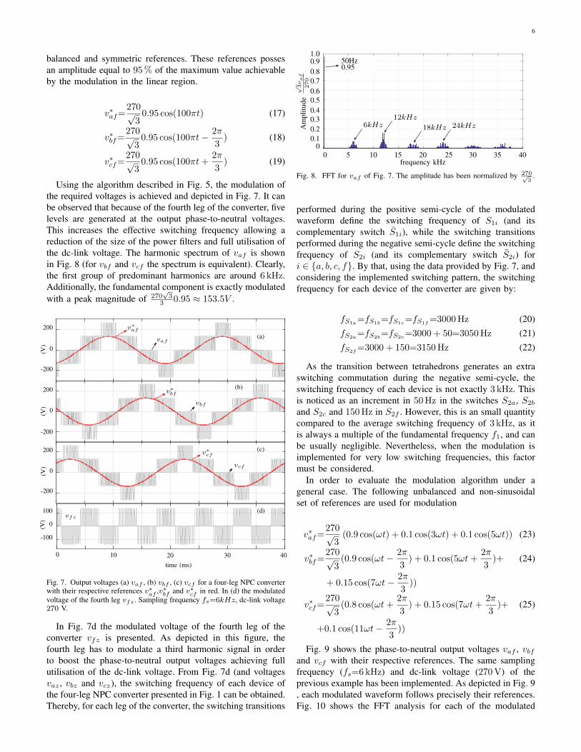
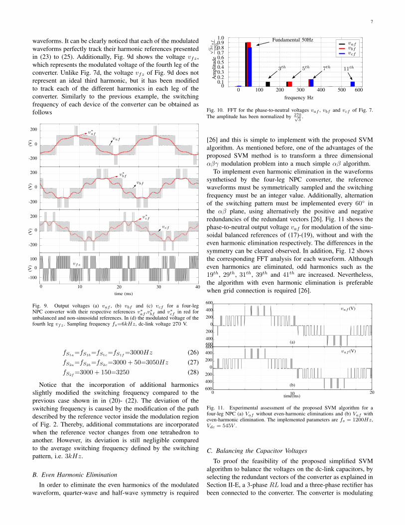
Using the algorithm described in Fig. 5, the modulation ofthe required voltages is achieved and depicted in Fig. 7. It canbe observed that because of the fourth leg of the converter, fivelevels are generated at the output phase-to-neutral voltages.This increases the effective switching frequency allowing areduction of the size of the power filters and full utilisation ofthe dc-link voltage. The harmonic spectrum of vaf is shownin Fig. 8 (for vbf and vcf the spectrum is equivalent). Clearly,the first group of predominant harmonics are around 6 kHz.Additionally, the fundamental component is exactly modulatedwith a peak magnitude of 270
√3
3 0.95 ≈ 153.5V .
0 10 20 30 40
-200
0
200
0
200
-200
-200
0
200
time (ms)
v∗af
v∗bf
v∗cf
vaf
vbf
vcf
(V)
(V)
(V)
-100
0
100vfz
(V)
(a)
(b)
(c)
(d)
Fig. 7. Output voltages (a) vaf , (b) vbf , (c) vcf for a four-leg NPC converterwith their respective references v∗af ,v∗bf and v∗cf in red. In (d) the modulatedvoltage of the fourth leg vfz . Sampling frequency fs=6kHz, dc-link voltage270 V.
In Fig. 7d the modulated voltage of the fourth leg of theconverter vfz is presented. As depicted in this figure, thefourth leg has to modulate a third harmonic signal in orderto boost the phase-to-neutral output voltages achieving fullutilisation of the dc-link voltage. From Fig. 7d (and voltagesvaz , vbz and vcz), the switching frequency of each device ofthe four-leg NPC converter presented in Fig. 1 can be obtained.Thereby, for each leg of the converter, the switching transitions
5 10 150 20 25 30 35 40frequency kHz
Am
plitu
de√3vaf
270
00.10.20.30.40.50.60.70.80.91.0
0.95
6kHz12kHz
18kHz 24kHz
50Hz
Fig. 8. FFT for vaf of Fig. 7. The amplitude has been normalized by 270√3
.
performed during the positive semi-cycle of the modulatedwaveform define the switching frequency of S1i (and itscomplementary switch S1i), while the switching transitionsperformed during the negative semi-cycle define the switchingfrequency of S2i (and its complementary switch S2i) fori ∈ a, b, c, f. By that, using the data provided by Fig. 7, andconsidering the implemented switching pattern, the switchingfrequency for each device of the converter are given by:
fS1a=fS1b=fS1c=fS1f
=3000 Hz (20)fS2a=fS2b
=fS2c=3000 + 50=3050 Hz (21)fS2f
=3000 + 150=3150 Hz (22)
As the transition between tetrahedrons generates an extraswitching commutation during the negative semi-cycle, theswitching frequency of each device is not exactly 3 kHz. Thisis noticed as an increment in 50 Hz in the switches S2a, S2b
and S2c and 150 Hz in S2f . However, this is an small quantitycompared to the average switching frequency of 3 kHz, as itis always a multiple of the fundamental frequency f1, and canbe usually negligible. Nevertheless, when the modulation isimplemented for very low switching frequencies, this factormust be considered.
In order to evaluate the modulation algorithm under ageneral case. The following unbalanced and non-sinusoidalset of references are used for modulation
v∗af=270√
3(0.9 cos(ωt) + 0.1 cos(3ωt) + 0.1 cos(5ωt)) (23)
v∗bf=270√
3(0.9 cos(ωt− 2π
3) + 0.1 cos(5ωt+
2π
3)+ (24)
+ 0.15 cos(7ωt− 2π
3))
v∗cf=270√
3(0.8 cos(ωt+
2π
3) + 0.15 cos(7ωt+
2π
3)+ (25)
+0.1 cos(11ωt− 2π
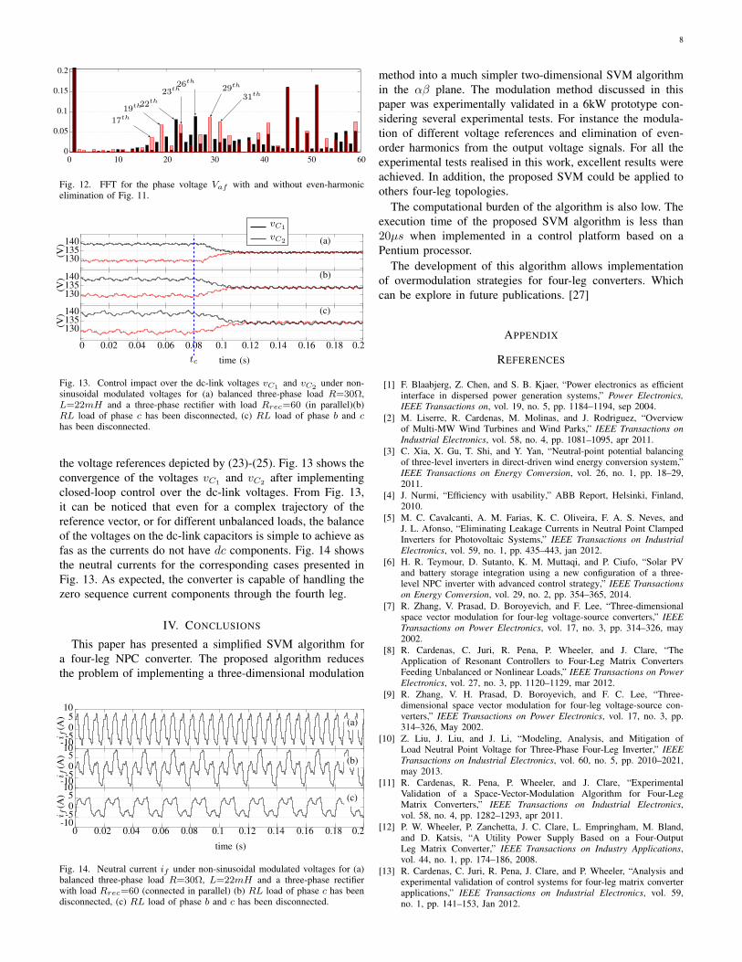
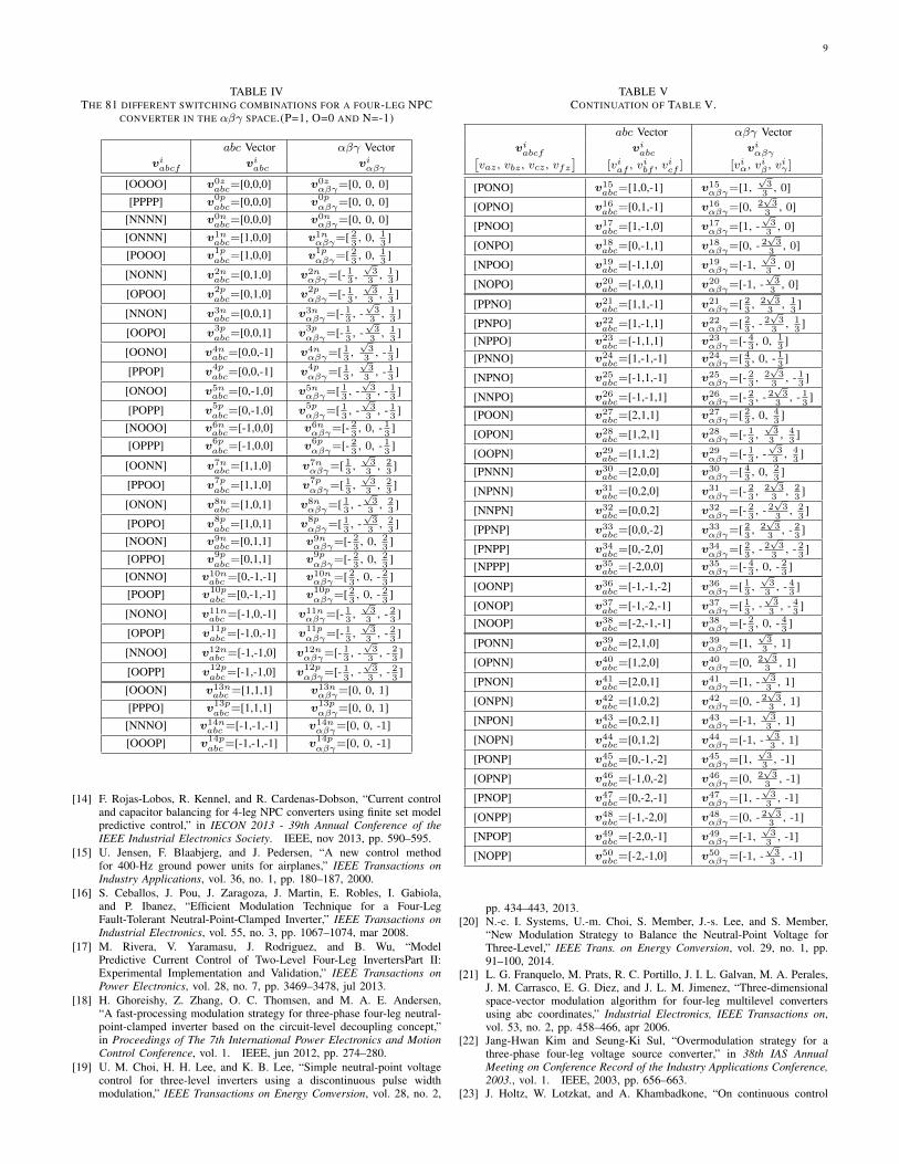
3))
Fig. 9 shows the phase-to-neutral output voltages vaf , vbfand vcf with their respective references. The same samplingfrequency (fs=6 kHz) and dc-link voltage (270 V) of theprevious example has been implemented. As depicted in Fig. 9, each modulated waveform follows precisely their references.Fig. 10 shows the FFT analysis for each of the modulated
7
waveforms. It can be clearly noticed that each of the modulatedwaveforms perfectly track their harmonic references presentedin (23) to (25). Additionally, Fig. 9d shows the voltage vfz ,which represents the modulated voltage of the fourth leg of theconverter. Unlike Fig. 7d, the voltage vfz of Fig. 9d does notrepresent an ideal third harmonic, but it has been modifiedto track each of the different harmonics in each leg of theconverter. Similarly to the previous example, the switchingfrequency of each device of the converter can be obtained asfollows
-200
0
200
0
200
-200
-200
0
200v∗af
v∗bf
v∗cf
vaf
vbf
vcf
(V)
(V)
(V)
0 10 20 30 40time (ms)
-100
0
100vfz
(V)
Fig. 9. Output voltages (a) vaf , (b) vbf and (c) vcf for a four-legNPC converter with their respective references v∗af ,v∗bf and v∗cf in red forunbalanced and non-sinusoidal references. In (d) the modulated voltage of thefourth leg vfz . Sampling frequency fs=6kHz, dc-link voltage 270 V.
fS1a=fS1b=fS1c=fS1f
=3000Hz (26)fS2a=fS2b
=fS2c=3000 + 50=3050Hz (27)fS2f
=3000 + 150=3250 (28)
Notice that the incorporation of additional harmonicsslightly modified the switching frequency compared to theprevious case shown in in (20)- (22). The deviation of theswitching frequency is caused by the modification of the pathdescribed by the reference vector inside the modulation regionof Fig. 2. Thereby, additional commutations are incorporatedwhen the reference vector changes from one tetrahedron toanother. However, its deviation is still negligible comparedto the average switching frequency defined by the switchingpattern, i.e. 3kHz.
B. Even Harmonic Elimination
In order to eliminate the even harmonics of the modulatedwaveform, quarter-wave and half-wave symmetry is required
0 100 200 300 400 500 600
Am
plitu
de√
3vaf
270
00.10.20.30.40.50.60.70.80.91.0
frequency Hz
Fundamental 50Hz
3th 5th 7th 11th
vafvbfvcf
Fig. 10. FFT for the phase-to-neutral voltages vaf , vbf and vcf of Fig. 7.The amplitude has been normalized by 270√
3.
[26] and this is simple to implement with the proposed SVMalgorithm. As mentioned before, one of the advantages of theproposed SVM method is to transform a three dimensionalαβγ modulation problem into a much simple αβ algorithm.
To implement even harmonic elimination in the waveformssynthetised by the four-leg NPC converter, the referencewaveforms must be symmetrically sampled and the switchingfrequency must be an integer value. Additionally, alternationof the switching pattern must be implemented every 60 inthe αβ plane, using alternatively the positive and negativeredundancies of the redundant vectors [26]. Fig. 11 shows thephase-to-neutral output voltage vaf for modulation of the sinu-soidal balanced references of (17)-(19), without and with theeven harmonic elimination respectively. The differences in thesymmetry can be cleared observed. In addition, Fig. 12 showsthe corresponding FFT analysis for each waveform. Althougheven harmonics are eliminated, odd harmonics such as the19th, 29th, 31th, 39th and 41th are increased. Nevertheless,the algorithm with even harmonic elimination is preferablewhen grid connection is required [26].
0 10 20600
400
200
0
200
400600
time(ms)
vaf (V)600400
200
0
200
400
600vaf (V)
(a)
(b)
Fig. 11. Experimental assessment of the proposed SVM algorithm for afour-leg NPC (a) Vaf without even-harmonic eliminations and (b) Vaf witheven-harmonic elimination. The implemented parameters are fs = 1200Hz,Vdc = 545V .
C. Balancing the Capacitor Voltages
To proof the feasibility of the proposed simplified SVMalgorithm to balance the voltages on the dc-link capacitors, byselecting the redundant vectors of the converter as explained inSection II-E, a 3-phase RL load and a three-phase rectifier hasbeen connected to the converter. The converter is modulating
8
0 10 20 30 40 50 600
0.05
0.1
0.15
0.2
17th19th
22th23th
26th 29th
31th
Fig. 12. FFT for the phase voltage Vaf with and without even-harmonicelimination of Fig. 11.
140
130135
140
130135
140
130135
0 0.02 0.04 0.06 0.08 0.1 0.12 0.14 0.16 0.18 0.2
time (s)
(a)
(b)
(c)
tc
vC1
vC2
(V)
(V)
(V)
Fig. 13. Control impact over the dc-link voltages vC1and vC2
under non-sinusoidal modulated voltages for (a) balanced three-phase load R=30Ω,L=22mH and a three-phase rectifier with load Rrec=60 (in parallel)(b)RL load of phase c has been disconnected, (c) RL load of phase b and chas been disconnected.
the voltage references depicted by (23)-(25). Fig. 13 shows theconvergence of the voltages vC1
and vC2after implementing
closed-loop control over the dc-link voltages. From Fig. 13,it can be noticed that even for a complex trajectory of thereference vector, or for different unbalanced loads, the balanceof the voltages on the dc-link capacitors is simple to achieve asfas as the currents do not have dc components. Fig. 14 showsthe neutral currents for the corresponding cases presented inFig. 13. As expected, the converter is capable of handling thezero sequence current components through the fourth leg.
IV. CONCLUSIONS
This paper has presented a simplified SVM algorithm fora four-leg NPC converter. The proposed algorithm reducesthe problem of implementing a three-dimensional modulation
05
10
-5-10
0 0.02 0.04 0.06 0.08 0.1 0.12 0.14 0.16 0.18 0.2
time (s)
05
10
-5-10
05
10
-5-10
(a)
(b)
(c)
i f(A
)i f
(A)
i f(A
)
Fig. 14. Neutral current if under non-sinusoidal modulated voltages for (a)balanced three-phase load R=30Ω, L=22mH and a three-phase rectifierwith load Rrec=60 (connected in parallel) (b) RL load of phase c has beendisconnected, (c) RL load of phase b and c has been disconnected.
method into a much simpler two-dimensional SVM algorithmin the αβ plane. The modulation method discussed in thispaper was experimentally validated in a 6kW prototype con-sidering several experimental tests. For instance the modula-tion of different voltage references and elimination of even-order harmonics from the output voltage signals. For all theexperimental tests realised in this work, excellent results wereachieved. In addition, the proposed SVM could be applied toothers four-leg topologies.
The computational burden of the algorithm is also low. Theexecution time of the proposed SVM algorithm is less than20µs when implemented in a control platform based on aPentium processor.
The development of this algorithm allows implementationof overmodulation strategies for four-leg converters. Whichcan be explore in future publications. [27]
APPENDIX
REFERENCES
[1] F. Blaabjerg, Z. Chen, and S. B. Kjaer, “Power electronics as efficientinterface in dispersed power generation systems,” Power Electronics,IEEE Transactions on, vol. 19, no. 5, pp. 1184–1194, sep 2004.
[2] M. Liserre, R. Cardenas, M. Molinas, and J. Rodriguez, “Overviewof Multi-MW Wind Turbines and Wind Parks,” IEEE Transactions onIndustrial Electronics, vol. 58, no. 4, pp. 1081–1095, apr 2011.
[3] C. Xia, X. Gu, T. Shi, and Y. Yan, “Neutral-point potential balancingof three-level inverters in direct-driven wind energy conversion system,”IEEE Transactions on Energy Conversion, vol. 26, no. 1, pp. 18–29,2011.
[4] J. Nurmi, “Efficiency with usability,” ABB Report, Helsinki, Finland,2010.
[5] M. C. Cavalcanti, A. M. Farias, K. C. Oliveira, F. A. S. Neves, andJ. L. Afonso, “Eliminating Leakage Currents in Neutral Point ClampedInverters for Photovoltaic Systems,” IEEE Transactions on IndustrialElectronics, vol. 59, no. 1, pp. 435–443, jan 2012.
[6] H. R. Teymour, D. Sutanto, K. M. Muttaqi, and P. Ciufo, “Solar PVand battery storage integration using a new configuration of a three-level NPC inverter with advanced control strategy,” IEEE Transactionson Energy Conversion, vol. 29, no. 2, pp. 354–365, 2014.
[7] R. Zhang, V. Prasad, D. Boroyevich, and F. Lee, “Three-dimensionalspace vector modulation for four-leg voltage-source converters,” IEEETransactions on Power Electronics, vol. 17, no. 3, pp. 314–326, may2002.
[8] R. Cardenas, C. Juri, R. Pena, P. Wheeler, and J. Clare, “TheApplication of Resonant Controllers to Four-Leg Matrix ConvertersFeeding Unbalanced or Nonlinear Loads,” IEEE Transactions on PowerElectronics, vol. 27, no. 3, pp. 1120–1129, mar 2012.
[9] R. Zhang, V. H. Prasad, D. Boroyevich, and F. C. Lee, “Three-dimensional space vector modulation for four-leg voltage-source con-verters,” IEEE Transactions on Power Electronics, vol. 17, no. 3, pp.314–326, May 2002.
[10] Z. Liu, J. Liu, and J. Li, “Modeling, Analysis, and Mitigation ofLoad Neutral Point Voltage for Three-Phase Four-Leg Inverter,” IEEETransactions on Industrial Electronics, vol. 60, no. 5, pp. 2010–2021,may 2013.
[11] R. Cardenas, R. Pena, P. Wheeler, and J. Clare, “ExperimentalValidation of a Space-Vector-Modulation Algorithm for Four-LegMatrix Converters,” IEEE Transactions on Industrial Electronics,vol. 58, no. 4, pp. 1282–1293, apr 2011.
[12] P. W. Wheeler, P. Zanchetta, J. C. Clare, L. Empringham, M. Bland,and D. Katsis, “A Utility Power Supply Based on a Four-OutputLeg Matrix Converter,” IEEE Transactions on Industry Applications,vol. 44, no. 1, pp. 174–186, 2008.
[13] R. Cardenas, C. Juri, R. Pena, J. Clare, and P. Wheeler, “Analysis andexperimental validation of control systems for four-leg matrix converterapplications,” IEEE Transactions on Industrial Electronics, vol. 59,no. 1, pp. 141–153, Jan 2012.
9
TABLE IVTHE 81 DIFFERENT SWITCHING COMBINATIONS FOR A FOUR-LEG NPC
CONVERTER IN THE αβγ SPACE.(P=1, O=0 AND N=-1)
abc Vector αβγ Vectorviabcf viabc viαβγ
[OOOO] v0zabc=[0,0,0] v0z
αβγ=[0, 0, 0]
[PPPP] v0pabc=[0,0,0] v0p
αβγ=[0, 0, 0][NNNN] v0n
abc=[0,0,0] v0nαβγ=[0, 0, 0]
[ONNN] v1nabc=[1,0,0] v1n
αβγ=[ 23
, 0, 13
]
[POOO] v1pabc=[1,0,0] v1p
αβγ=[ 23
, 0, 13
]
[NONN] v2nabc=[0,1,0] v2n
αβγ=[- 13
,√3
3, 13
]
[OPOO] v2pabc=[0,1,0] v2p
αβγ=[- 13
,√3
3, 13
]
[NNON] v3nabc=[0,0,1] v3n
αβγ=[- 13
, -√3
3, 13
]
[OOPO] v3pabc=[0,0,1] v3p
αβγ=[- 13
, -√3
3, 13
]
[OONO] v4nabc=[0,0,-1] v4n
αβγ=[ 13
,√3
3, - 1
3]
[PPOP] v4pabc=[0,0,-1] v4p
αβγ=[ 13
,√3
3, - 1
3]
[ONOO] v5nabc=[0,-1,0] v5n
αβγ=[ 13
, -√
33
, - 13
]
[POPP] v5pabc=[0,-1,0] v5p
αβγ=[ 13
, -√
33
, - 13
][NOOO] v6n
abc=[-1,0,0] v6nαβγ=[- 2
3, 0, - 1
3]
[OPPP] v6pabc=[-1,0,0] v6p
αβγ=[- 23
, 0, - 13
]
[OONN] v7nabc=[1,1,0] v7n
αβγ=[ 13
,√3
3, 2
3]
[PPOO] v7pabc=[1,1,0] v7p
αβγ=[ 13
,√3
3, 2
3]
[ONON] v8nabc=[1,0,1] v8n
αβγ=[ 13
, -√
33
, 23
]
[POPO] v8pabc=[1,0,1] v8p
αβγ=[ 13
, -√
33
, 23
][NOON] v9n
abc=[0,1,1] v9nαβγ=[- 2
3, 0, 2
3]
[OPPO] v9pabc=[0,1,1] v9p
αβγ=[- 23
, 0, 23
][ONNO] v10n
abc =[0,-1,-1] v10nαβγ=[ 2
3, 0, - 2
3]
[POOP] v10pabc=[0,-1,-1] v10p
αβγ=[ 23
, 0, - 23
]
[NONO] v11nabc =[-1,0,-1] v11n
αβγ=[- 13
,√3
3, - 2
3]
[OPOP] v11pabc=[-1,0,-1] v11p
αβγ=[- 13
,√3
3, - 2
3]
[NNOO] v12nabc =[-1,-1,0] v12n
αβγ=[- 13
, -√
33
, - 23
]
[OOPP] v12pabc=[-1,-1,0] v12p
αβγ=[- 13
, -√
33
, - 23
]
[OOON] v13nabc =[1,1,1] v13n
αβγ=[0, 0, 1]
[PPPO] v13pabc=[1,1,1] v13p
αβγ=[0, 0, 1][NNNO] v14n
abc =[-1,-1,-1] v14nαβγ=[0, 0, -1]
[OOOP] v14pabc=[-1,-1,-1] v14p
αβγ=[0, 0, -1]
[14] F. Rojas-Lobos, R. Kennel, and R. Cardenas-Dobson, “Current controland capacitor balancing for 4-leg NPC converters using finite set modelpredictive control,” in IECON 2013 - 39th Annual Conference of theIEEE Industrial Electronics Society. IEEE, nov 2013, pp. 590–595.
[15] U. Jensen, F. Blaabjerg, and J. Pedersen, “A new control methodfor 400-Hz ground power units for airplanes,” IEEE Transactions onIndustry Applications, vol. 36, no. 1, pp. 180–187, 2000.
[16] S. Ceballos, J. Pou, J. Zaragoza, J. Martin, E. Robles, I. Gabiola,and P. Ibanez, “Efficient Modulation Technique for a Four-LegFault-Tolerant Neutral-Point-Clamped Inverter,” IEEE Transactions onIndustrial Electronics, vol. 55, no. 3, pp. 1067–1074, mar 2008.
[17] M. Rivera, V. Yaramasu, J. Rodriguez, and B. Wu, “ModelPredictive Current Control of Two-Level Four-Leg InvertersPart II:Experimental Implementation and Validation,” IEEE Transactions onPower Electronics, vol. 28, no. 7, pp. 3469–3478, jul 2013.
[18] H. Ghoreishy, Z. Zhang, O. C. Thomsen, and M. A. E. Andersen,“A fast-processing modulation strategy for three-phase four-leg neutral-point-clamped inverter based on the circuit-level decoupling concept,”in Proceedings of The 7th International Power Electronics and MotionControl Conference, vol. 1. IEEE, jun 2012, pp. 274–280.
[19] U. M. Choi, H. H. Lee, and K. B. Lee, “Simple neutral-point voltagecontrol for three-level inverters using a discontinuous pulse widthmodulation,” IEEE Transactions on Energy Conversion, vol. 28, no. 2,
TABLE VCONTINUATION OF TABLE V.
abc Vector αβγ Vectorviabcf viabc viαβγ[
vaz , vbz , vcz , vfz]
[viaf , vibf , vicf ] [viα, viβ , viγ ]
[PONO] v15abc=[1,0,-1] v15
αβγ=[1,√
33
, 0]
[OPNO] v16abc=[0,1,-1] v16
αβγ=[0, 2√
33
, 0]
[PNOO] v17abc=[1,-1,0] v17
αβγ=[1, -√
33
, 0]
[ONPO] v18abc=[0,-1,1] v18
αβγ=[0, - 2√
33
, 0]
[NPOO] v19abc=[-1,1,0] v19
αβγ=[-1,√3
3, 0]
[NOPO] v20abc=[-1,0,1] v20
αβγ=[-1, -√3
3, 0]
[PPNO] v21abc=[1,1,-1] v21
αβγ=[ 23
, 2√3
3, 1
3]
[PNPO] v22abc=[1,-1,1] v22
αβγ=[ 23
, - 2√
33
, 13
][NPPO] v23
abc=[-1,1,1] v23αβγ=[- 4
3, 0, 1
3]
[PNNO] v24abc=[1,-1,-1] v24
αβγ=[ 43
, 0, - 13
]
[NPNO] v25abc=[-1,1,-1] v25
αβγ=[- 23
, 2√3
3, - 1
3]
[NNPO] v26abc=[-1,-1,1] v26
αβγ=[- 23
, - 2√3
3, - 1
3]
[POON] v27abc=[2,1,1] v27
αβγ=[ 23
, 0, 43
]
[OPON] v28abc=[1,2,1] v28
αβγ=[- 13
,√3
3, 4
3]
[OOPN] v29abc=[1,1,2] v29
αβγ=[- 13
, -√3
3, 4
3]
[PNNN] v30abc=[2,0,0] v30
αβγ=[ 43
, 0, 23
]
[NPNN] v31abc=[0,2,0] v31
αβγ=[- 23
, 2√3
3, 2
3]
[NNPN] v32abc=[0,0,2] v32
αβγ=[- 23
, - 2√3
3, 23
]
[PPNP] v33abc=[0,0,-2] v33
αβγ=[ 23
, 2√3
3, - 2
3]
[PNPP] v34abc=[0,-2,0] v34
αβγ=[ 23
, - 2√
33
, - 23
][NPPP] v35
abc=[-2,0,0] v35αβγ=[- 4
3, 0, - 2
3]
[OONP] v36abc=[-1,-1,-2] v36
αβγ=[ 13
,√
33
, - 43
]
[ONOP] v37abc=[-1,-2,-1] v37
αβγ=[ 13
, -√
33
, - 43
][NOOP] v38
abc=[-2,-1,-1] v38αβγ=[- 2
3, 0, - 4
3]
[PONN] v39abc=[2,1,0] v39
αβγ=[1,√
33
, 1]
[OPNN] v40abc=[1,2,0] v40
αβγ=[0, 2√
33
, 1]
[PNON] v41abc=[2,0,1] v41
αβγ=[1, -√
33
, 1]
[ONPN] v42abc=[1,0,2] v42
αβγ=[0, - 2√
33
, 1]
[NPON] v43abc=[0,2,1] v43
αβγ=[-1,√3
3, 1]
[NOPN] v44abc=[0,1,2] v44
αβγ=[-1, -√3
3, 1]
[PONP] v45abc=[0,-1,-2] v45
αβγ=[1,√
33
, -1]
[OPNP] v46abc=[-1,0,-2] v46
αβγ=[0, 2√
33
, -1]
[PNOP] v47abc=[0,-2,-1] v47
αβγ=[1, -√
33
, -1]
[ONPP] v48abc=[-1,-2,0] v48
αβγ=[0, - 2√
33
, -1]
[NPOP] v49abc=[-2,0,-1] v49
αβγ=[-1,√3
3, -1]
[NOPP] v50abc=[-2,-1,0] v50
αβγ=[-1, -√3
3, -1]
pp. 434–443, 2013.[20] N.-c. I. Systems, U.-m. Choi, S. Member, J.-s. Lee, and S. Member,
“New Modulation Strategy to Balance the Neutral-Point Voltage forThree-Level,” IEEE Trans. on Energy Conversion, vol. 29, no. 1, pp.91–100, 2014.
[21] L. G. Franquelo, M. Prats, R. C. Portillo, J. I. L. Galvan, M. A. Perales,J. M. Carrasco, E. G. Diez, and J. L. M. Jimenez, “Three-dimensionalspace-vector modulation algorithm for four-leg multilevel convertersusing abc coordinates,” Industrial Electronics, IEEE Transactions on,vol. 53, no. 2, pp. 458–466, apr 2006.
[22] Jang-Hwan Kim and Seung-Ki Sul, “Overmodulation strategy for athree-phase four-leg voltage source converter,” in 38th IAS AnnualMeeting on Conference Record of the Industry Applications Conference,2003., vol. 1. IEEE, 2003, pp. 656–663.
[23] J. Holtz, W. Lotzkat, and A. Khambadkone, “On continuous control
10
of PWM inverters in the overmodulation range including the six-step mode,” in Proceedings of the 1992 International Conferenceon Industrial Electronics, Control, Instrumentation, and Automation.IEEE, 1992, pp. 307–312.
[24] D. Feng and D. Xu, “Space vector modulation for neutral pointclamped multilevel inverter with even order harmonic elimination,” inCanadian Conference on Electrical and Computer Engineering 2004(IEEE Cat. No.04CH37513), vol. 3. IEEE, 2004, pp. 1471–1475.
[25] “519-1992 - IEEE Recommended Practices and Requirements for Har-monic Control in Electrical Power Systems.”
[26] B. Wu, High-Power Converters and AC Drives. Wiley, 2005.[27] N. Celanovic and D. Boroyevich, “A comprehensive study of neutral-
point voltage balancing problem in three-level neutral-point-clampedvoltage source pwm inverters,” IEEE Transactions on Power Electronics,vol. 15, no. 2, pp. 242–249, Mar 2000.
Felix Rojas was born in Santiago, Chile. He re-ceived the B.Eng. and M.Sc. degrees in electricalengineering with honours in 2009, from the Univer-sidad de Santiago de Chile. In 2015, he obtainedhis doctoral degree from the Technical University ofMunich, Germany. During his career, he has workedin research projects related to Active filter for rail-way Applications, Matrix Converters and Multilevelconverters for distribution systems. Currently he isfull time lecturer at the University of Santiago, Chile.His research interest are Multilevel converters for
power network conditioning.
Ralph Kennel (M’90-SM’96) received the diplomadegree in 1979 and the Dr.-Ing. (Ph.D.) degree in1984 from the University of Kaiserslautern, Kaiser-slautern, Germany. From 1983 to 1999, he workedon several positions with Robert BOSCH GmbH,Stuttgart, Germany. Until 1997, he was responsiblefor the development of servo drives. From 1994 to1999, he was appointed as a Visiting Professor at theUniversity of Newcastleupon-Tyne, England, U.K.From 1999 to 2008, he was a Professor for elec-trical machines and drives at Wuppertal University,
Wuppertal, Germany. Since 2008, he has been a Professor for electrical drivesystems and power electronics at Technische Universtat Muenchen, Germany.His main interests today are: sensorless control of ac drives, predictive controlof power electronics, and hardware-in-the-Loop systems.
Jon C. Clare (M’90-SM’04) was born in Bristol,U.K., in 1957. He received the B.Sc. and Ph.D.degrees in electrical engineering from the Universityof Bristol, Bristol. From 1984 to 1990, he was aResearch Assistant and Lecturer with the Universityof Bristol, where he was involved in teaching andresearch on power electronic systems. Since 1990,he has been with the Power Electronics, Machinesand Control Group, The University of Nottingham,Nottingham, U.K., where he is currently a Professorof power electronics. His research interests include
power-electronic converters and modulation strategies, variable-speed-drivesystems, and electromagnetic compatibility.
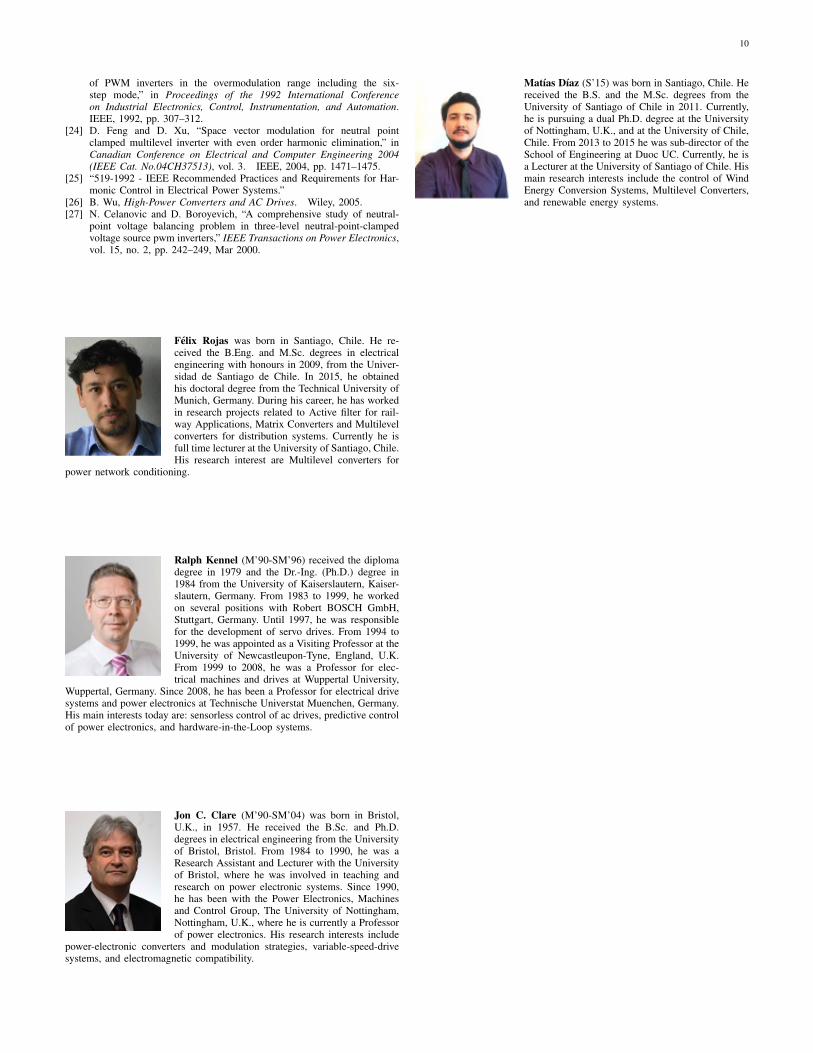
Matıas Dıaz (S’15) was born in Santiago, Chile. Hereceived the B.S. and the M.Sc. degrees from theUniversity of Santiago of Chile in 2011. Currently,he is pursuing a dual Ph.D. degree at the Universityof Nottingham, U.K., and at the University of Chile,Chile. From 2013 to 2015 he was sub-director of theSchool of Engineering at Duoc UC. Currently, he isa Lecturer at the University of Santiago of Chile. Hismain research interests include the control of WindEnergy Conversion Systems, Multilevel Converters,and renewable energy systems.


![Proposed syllabus for 1st Year 1st semester Mathematical ...bgc.org.in/pdf/LESSON-PLAN/VARIOUS/Physics_Lesson... · Vector Space and Matrices [JM-15] (a) Vector Space: Vector space:](https://img.pdfslide.us/doc/110x75/5e999f563db3180a39619752/proposed-syllabus-for-1st-year-1st-semester-mathematical-bgcorginpdflesson-planvariousphysicslesson.jpg)