Embed Size (px)
Citation preview

Craig Sainsbury +61(3)9679-1778
[email protected] Sachs Australia Pty Ltd.
Goldman Sachs does and seeks to do business with companies covered in its research reports. As aresult, investors should be aware that the firm may have a conflict of interest that could affect theobjectivity of this report. Investors should consider this report as only a single factor in making theirinvestment decision. For Reg AC certification and other important disclosures, see the DisclosureAppendix, or go to www.gs.com/research/hedge.html. Analysts employed by non-US affiliates are notregistered/qualified as research analysts with FINRA in the U.S.
The Goldman Sachs Group, Inc.
EQUITY RESEARCH | September 27, 2016
Faster, Stronger, Smaller, Lighter
P R O F I L E S I N I N N O V A T I O NAdvanced Materials
Jay Shyam, CFA+61(3)9679-1972
[email protected] Sachs Australia Pty Ltd.
Shuhei Nakamura +81(3)6437-9932
[email protected] Sachs Japan Co., Ltd.
Toshiya Hari (646) 446-1759
[email protected], Sachs & Co.
Marcus Shin+82(2)3788-1154
[email protected] Sachs (Asia) L.L.C., Seoul Branch
Innovation isn’t always digital. Theinsatiable need to make products faster,stronger, smaller and lighter is driving thedevelopment of new and enhancedAdvanced Materials with properties out ofreach of prior generations. In this report,the latest in our Profiles in Innovationseries, we explore where AdvancedMaterials science is on the cusp ofbreaking new boundaries and making theleap to commercialisation, and we chartthe interconnected global ecosystem ofpublic and private companies ripe fordisruption. We hone in on advances in fourkey areas—Nanotechnology, Graphene,OLEDs and Cheating Moore’s Law—thatcan address some of the biggest businesschallenges of the day, from rolling out a 5Gnetwork to improving the efficacy ofcancer drugs to creating energy storage solutions.
For t
he e
xclu
sive
use
of M
IHAI
L_TU
RLAK
OV@
SBER
BANK
-CIB
.RU

September 27, 2016 Profiles in Innovation
Goldman Sachs Global Investment Research 2
Table of contents
Executive summary: The DNA of Disruption 3
Advanced materials in numbers 7
Key players 8
Overview of our case studies 9
Nanotechnology: A very small big deal 11 Nanotechnology – the materials toolbox of the 21ST century 12 The benefits of nanotechnology: The world’s building blocks 13 Nanomanufacturing: A bottom-up future 14 The nanotech microscope evolution 17 Commercialising nanotechnology 18 Additives – the here and now of nanotechnology 19
Graphene 21 The history of graphene and its benefits 22 The buckyball – Generation X’s cautionary tale on graphene 23 Where’s my Indium? 26 Graphene manufacturing processes 27 Potential applications for graphene 29
OLEDs: Bending the future 31 A brief history of OLEDs and why they matter 32 The hype: Present-day applications already attractive 34 The promise: Mobile technology, all roads lead to OLEDs 35 The future of television: OLEDs or quantum dots? 37 3D TVs: A cautionary tale 39
Cheating Moore’s Law 41 Semiconductors 101 43 Getting smaller & smaller… a history of process improvement 44 Materials and construction to help cheat Moore’s Law 46 Commercialising the evolution of the semiconductor 49
Case studies 51 Water filtration: Creating a sustainable future 52 Energy storage: The shift to renewables 54 Nanomedicine: A plethora of possibility 56 5G communications: Speeding up the future 62 An interview with Dr. John Chen, Phoenix Venture Partners 65
Disclosure Appendix 67
Contributing authors: Craig Sainsbury; Jay Shyam, CFA; Shuhei Nakamura; Toshiya Hari; Charles Long; Marcus Shin;
Robert D. Boroujerdi; Hugo Scott-Gall; Brian Rooney; Shin Horie; Richard Manley; Ian Abbott; Brian Lee, CFA; Matthew
McNee; Grace Fulton; Giuni Lee; Ken Lek; Ayaka Misonou; Frank He; Julian Zhu; Peter Callahan; Eddie Ow, CFA; Anita
Dinshaw; Isabelle Dawson
This is the sixth report in our Profiles in Innovation series analyzing emerging technologies that are creating profit
pools and disrupting old ones. Access previous reports in the series below or visit our portal to learn more and see
related resources.
• Virtual and Augmented Reality
• Drones
• Factory of the Future
• Blockchain
• Precision Farming
Get a 3-minute audio summary of this report from author Craig Sainsbury. Listen here
For t
he e
xclu
sive
use
of M
IHAI
L_TU
RLAK
OV@
SBER
BANK
-CIB
.RU

September 27, 2016 Profiles in Innovation
Goldman Sachs Global Investment Research 3
Executive summary: The DNA of Disruption
Historians often refer to pivotal eras in human history by the materials that dominated
them ‒ most notably, the Stone Age, the Bronze Age, and the Iron Age. Those times are
long past, however, and modern man finds it easy to believe the current era of human
history, the Digital Age, is held up by more abstract pillars ‒ like intellect, innovation or
communication. But that is only partly correct.
Materials remain crucial to human progress, and advanced materials (AMs) are the DNA of
disruption for things ‒ from the largest structures to the smallest electronic components.
Each revolution in semiconductors, metals, polymers, ceramics and other substances has
created and transformed new products and industries. Just as materials like concrete,
Velcro, Gore-Tex, plastic and aluminum were considered advanced at one point in time,
today the need to make products faster, stronger, smaller, and lighter has driven the
development of materials with properties out of reach of previous generations. Yet AMs
are spread so widely across industries, and their development and adoption is so uneven,
that the investment implications are exceptionally wide-ranging and can impact almost any
market. In this report ‒ the latest in our Profiles in Innovation series ‒ we focus on four
areas that we believe have the greatest chance of commercial impact:
1) Nanotechnology: The ability to understand and utilize the properties of materials at a
molecular level (an atom is 0.1nm wide) has the potential to offer benefits such as size
reduction and specialty material construction to continue to drive R&D and new
product creation.
2) Graphene: An allotrope of carbon, with properties of strength, conductivity and
transparency that stem from its unique 2D structure, is showing potential in a myriad
of applications from water filtration to semiconductors.
3) OLEDs utilise an organic compound based electroluminescent layer to emit light.
Smartphones and TVs have already taken advantage of their superior display and
flexibility, creating a pathway for new products that can fundamentally change mobile
technology and the consumer experience.
4) Cheating Moore’s Law, where the constant effort to fit more transistors onto smaller
chips is fueling the drive for new materials.
Exhibit 1: The development of AMs is driven by both push and pull forces
Source: Company data, Goldman Sachs Global Investment Research.
We explore how AMs can help solve critical real-world challenges—from water filtration to energy storage—in four case studies on pages 51 to 63.
For t
he e
xclu
sive
use
of M
IHAI
L_TU
RLAK
OV@
SBER
BANK
-CIB
.RU

September 27, 2016 Profiles in Innovation
Goldman Sachs Global Investment Research 4
Why Advanced Materials and why now?
The benefits of new materials run the gamut from lowering costs by substituting for
something else to introducing capabilities that were previously impossible. History shows
the impact when an AM reaches widespread adoption, from the development of cement
and vulcanized rubber in the 19th century to stainless steel and nylon in the 20th.
Exhibit 2: A history of innovation through Advanced Materials
Source: Goldman Sachs Global Investment Research.
Year Advanced Material developed/created/discovered Creator/Developer
1824 Cement Joseph Aspdin
1825 Metallic alluminum produced Hans Christian Orsted
1839 Vulcanised Rubber Charles Goodyear
1839 Polystyrene Eduard Simon
1843 Vulcanite Thomas Hancock
1856 Celluloid Alexander Parkes
1879 Carbon Fiber Thomas Edison
1908 Cellophane Jacques E. Brandenberger
1909 Bakelite hard thermosetting plastic Leo Baekeland
1911 Superconductivity Heike Kamerlingh Onnes
1912 Stainless steel Harry Brearley
1924 Pyrex Corning Incorporated (Company)
1927 LED Oleg Losev
1931 Neoprene Julius Nieuwland
1931 Nylon Wallace Carothers
1935 LDPE Reginald Gibson/ Eric Fawcett
1938 Teflon (poly-tetrafluoroethylene) Roy Plunkett
1938 Fiberglass Owens Corning
1940 Titanium Sponge William Kroll
1941 Polyester W.K. Birtwhistle/ C.G. Ritchiethey
1947 Surgicel Ethicon (company)
1951 Velcro George de Mestral
1951 HDPE Paul Hogan/ Robert Banks
1954 Silicon solar cells Bell Laboratories (Company)
1954 Argon oxygen decarburization (AOD) refining Union Carbide Corporation (company)
1954 Styrofoam Ray McIntire
1958 Lycra Joseph Shivers
1959 Micropore 3M
1963 Gladwrap (shrink wrap) Dr Douglas Lyons Ford
1965 KEVLAR Stephanie Kwolek
1966 Gore-Tex Wilbert L Gore/ Robert W Gore
1968 Liquid crystal display (LCD) RCA (company
1970 Silica optical fibers Corning Incorporated (Company)
1970 Blu tack Alan Holloway
1974 Vicryl (polyglactin 910) Ethicon (company)
1982 PEEK Imperial Chemical Industries
1985 Fullerene molecule discovery Rice University
1985 Buckypaper Robert Curl/ Harold Kroto/ Richard Smalley
1986 First high temperature superconductor Alex Muller/ Georg Bednorz
1987 OLED Ching W Tang & Steven Van Slyke
1980s Zylon SRI International
1991 Lithium-Ion battery Sony Corporation
1991 Carbon Nanotubes Sumio Iijima
1993 Smart Pill Jerome Schentag
1994 Quantum Cascade Laser Bell Labs
1995 CMOS image sensor Eric Fossum
1998 Silicone Hydrogel Various
1990s M-5 (PIPD fibre) Akzo Nobel
1990s Vectran Celanese Acetate LLC
1990s Precious Metal Clay Masaki Morikawa
2001 Artificial liver Dr Kenneth Matsumura & Alin Foundation
2002 Nanotex Dr David Soane
2004 Graphene Andre Geim & Konstantin Novoselov
2007 Nanowire battery Various
For t
he e
xclu
sive
use
of M
IHAI
L_TU
RLAK
OV@
SBER
BANK
-CIB
.RU

September 27, 2016 Profiles in Innovation
Goldman Sachs Global Investment Research 5
Whilst the path to success for a new material can often be winding and slow, new
materials’ ability to transform industry norms is massive. Indeed some of today’s
promising materials, such as graphene, have yet to fulfill their potential. Nevertheless, we
see multiple drivers in place that give us confidence that today’s wave of R&D in new
materials will overcome the hurdles to make a significant impact across industries. These
drivers include:
Miniaturization and the race to squeeze more capabilities into ever-smaller devices.
The urgent need to replace dwindling critical resources, such as clean water (see page
52) and rare earth metals like indium (see page 26).
Environmental concerns and demand to reduce energy use and waste.
The next generation of AMs is set to be driven by the intertwined and symbiotic
relationship between technology and materials science. On the one hand, the massive
advancement in computing power over the past 20 years gives scientists and
manufacturers the ability to study and structure materials at nano-scales. At the same time,
constant increases in computer power place pressure on the effort to continue doubling the
number of transistors that can be squeezed into a square inch of integrated circuit (as per
Moore’s Law). Thus, one of the key enablers of the modern development of AMs is itself
dependent on the successful development of new materials.
Out of the lab, into the world: Where can Advanced Materials make
a difference?
With the timing right for key AMs to make their mark, we offer case studies of four high-
impact applications:
1. Water filtration: With more than 600mn people living without access to potable water
and safe sanitation, quality water filtration has the ability to transform society as a
whole. Graphene filtration technologies can enhance existing filtration systems with
improved speed, scale and costs. With US$10bn spent annually on emerging country
water quality and US$90bn on bottled water globally, the financial opportunity is
significant.
2. Energy storage: Continued advances in energy storage and efficiency are key to
managing the demands of a growing population and curbing carbon emissions.
Nanotech is set to play a vital role in this effort, with the potential to rapidly improve
battery charge times and performance.
3. Nanomedicine: Prescription drugs have been a key part of medicinal recuperation for
decades, but nanotech has the potential to make them safer and more precise by
engineering pills to target impacted areas instead of the whole body. For cancer
patients, that means chemotherapy could be delivered directly to the impacted tumor
cells, lessening the side effects and potentially speeding recovery. With the cancer
drug market a US$100bn industry, nanotech has the ability to generate significant
value for companies that can commercialise the technology.
4. Next-gen communications: The coming 5G revolution will increase demand for
materials capable of handling high-spectrum frequencies up to 100GHz. Gallium nitride
fits this bill, offering better performance than traditional silicon-based technologies on
the market today. Its higher bandgap and ability to withstand higher voltages also
make it attractive to chip companies working in defense applications.
We highlight public and private company exposures to Advanced Material development in our ecosystem on page 8.
Advanced Materials have now penetrated the VC space; we interview Dr. John Chen, managing partner of an AM venture capital firm, on page 65.
For t
he e
xclu
sive
use
of M
IHAI
L_TU
RLAK
OV@
SBER
BANK
-CIB
.RU

September 27, 2016 Profiles in Innovation
Goldman Sachs Global Investment Research 6
Exhibit 3: Revolution is dependent on symbiosis Technology and materials cycle
Exhibit 4: AMs are not isolated silos with many of the
materials and processes used in transformational
technology
Source: Goldman Sachs Global Investment Research.
Source: Goldman Sachs Global Investment Research.
We highlight public and private players at the intersection of promising AM technology and
the case studies we detail on pages 50-63, as well as incumbents at risk. The corporations
exposed to the sector are a mix of generalist innovators (such as Samsung, 3M, Lockheed
Martin, and BASF) and specialist innovators that are predominantly emerging unlisted
corporations (such as Cyclics Corporation, Graphene Laboratories, and Solicore).
For t
he e
xclu
sive
use
of M
IHAI
L_TU
RLAK
OV@
SBER
BANK
-CIB
.RU

ADVANCED MATERIALS in numbers
The strength of single-layer graphene compared to steel. (p. 24)
300x
The year nanotechnology—the concept of
engineering materials with atomic
precision—was first discussed. (p. 13) 1959
The year graphene—a material that classifies as a subset of
nanotechnology and a cousin of the common LCD material
graphite—was first isolated in its critical single-layer form. (p.
22)
2004
Graphene’s electrical current density compared to copper, a
commonly used material in semiconductors. 25% of patents filed
for graphene so far relate to semiconductor technology. (p. 24)
10,000,000x
The viewing angle smartphones could
offer by using flexible OLED
displays—essentially the ability to fold
your smartphone in half and open it to
lay flat. (p. 32)
180˚
VISUALIZING NANOPARTICLES: SMALL SIZE, BIG AREA
The diameter of a hair follicle in nanometers. (p. 12) 75,000
25,400,000 An inch in nanometers. (p. 12)
1,536 mm2
9,600 m2
The (limited) number of registered
products that use nanoparticles today. (p.
19) 1,944
THE LONG WINDUP IN NANOTECH
A ‘MIRACLE MATERIAL’ OF A COUSIN
90%
The decline in graphene production costs in the past three years.
We estimate costs need to fall another 90% to make graphene
commercially competitive. (p. 27)
A BENDABLE SMARTPHONE
The electron mobility advantage of III-V
materials (materials containing elements
from groups III and V of the periodic
table) relative to silicon, the current
material of choice in semiconductors.
Companies are seeking to integrate III-V
materials in chips to improve processing
power. (p. 47)
50x
FASTER COMPUTING
$25
billion
Our estimate for the total addressable
market for OLEDs by 2018. (p. 34)
The surface area of a standard playing dice. (p. 14)
The surface area of a standard playing dice when deconstructed into its nanoparticle components.
That’s the equivalent of 8 Olympic-sized swimming pools. (p. 14)
For t
he e
xclu
sive
use
of M
IHAI
L_TU
RLAK
OV@
SBER
BANK
-CIB
.RU

The EcosystemAdvanced Materials - Key Players
Leading Conglomerates Samsung3MLockheed MartinBASFJohnson MattheyNokiaBayerShowa DenkoToshibaL'Oreal
Advanced Chips XXXXXX
GrapheneGraphenaGraphene LaborotoriesShowa DenkoFuture CarbonAngstrom MaterialsCVD Equipment corporationAMO GmbHApplied Graphene Materials
Nano CoatingsCetelon NanotechnikNnaovere TechnologiesDiamon-Fusion International
Nanomedicine & NanobiologyXXXXXX
OLED Samsung ElectronicsLGAppleUniversal displayApplied MaterialsUlvac
Nano SolarEcoark HoldingsSolicorePlextronics3MUniversal Display CorpQD Vision Inc
NanocompositesAlanod-Solar3M ESPEElementis ArkemaCyclics CorporationDu PontShowa Denko
A sample of companies with exposure
private company
Advanced Materials - Key PlayersA sample of companies with exposure
private company
NanocompositesAlanod-Solar3M ESPEElementis ArkemaCyclics CorporationDuPontShowa DenkoPentairKochSony
Nanomedicine & NanobiologyMerrimack PharmaceuticalsIntellia TherapeuticsEditas MedicineEli LillyFujifilmKonica MinoltaNanoCarrier3-D Matrix CellSeed
Advanced ChipsTokyo Electron
Cheating Moore’s LawIntelTSMCSamsung ElectronicsApplied MaterialsLam ResearchASMLTokyo ElectronQorvoMACOM
Generalist InvestorsSamsung Electronics3MLockheed MartinBASFJohnson MattheyNokiaBayerToray IndustriesL'OrealGE
GrapheneGrapheneaGraphene 3D LabGraphene LaboratoriesFutureCarbonAngstron MaterialsCVD Equipment CorporationAMO GmbHApplied Graphene MaterialsDongxu Optoelectronic Technology (000413.SZ)Xinjiang Zhongtai Chemical (002092.SZ)China Baoan Group (000009.SZ)Suzhou Jinfu New Material (300128.SZ)Haydale Graphene IndustriesDirecta PlusGraphene NanochemOCSiAlAbalonyx ASVorbeck MaterialsZapnGoAdvanced Graphene ProductsNanoXploreRS MinesGraphene Platform CorpElcora Advanced MaterialsChina Carbon Graphite GroupOsaka GasHEAD BVVittoriaYonex (Carbon nanotubes)
OLED Samsung ElectronicsLGAppleUniversal Display Applied MaterialsULVAC Valiant (002643.SZ)Puyang Huicheng (300481.SZ)Kangde Xin (002450.SZ)Sino Wealth Electronic (300327.SZ)Truly International (732.HK)Idemitsu Kosan (5019.T)Merck KGaACoherentCanon Konica MinoltaNissha PrintingJapan DisplaySharpSCREEN HoldingsSonyToshibaDai Nippon PrintingV-TechnologyFerrotec Hirata
NanosolarEcoArk BrightVolt (Solicore)Solvay (Plextronics)3MUniversal Display QD Vision
NanocoatingsP2iDowSiemensCetelon NanotechnikNanovere TechnologiesDiamon-Fusion International
For t
he e
xclu
sive
use
of M
IHAI
L_TU
RLAK
OV@
SBER
BANK
-CIB
.RU

The EcosystemAdvanced Materials - Use Cases
Advanced materials used: Nanotechnology, graphene
How it works: Graphene oxide membranes are impermeable to all gases and vapors besides water, allowing for faster and better filtration. Select enablers/disrupters: Lockheed Martin, Dow, GE, Pentair, 3M, Koch, SiemensIncumbents at risk: Bottled water companies
Water Filtration
Advanced materials used: Nanotechnology, graphene, OLED
How it works: Nanotechnology can enhance the properties of bulk materials like fuel cells, solar cells and lithium ion batteries to improve their storage potential and recharge rates. Select enablers/disrupters: Sony, Toshiba, Manz, BASF, 3M, DuPontIncumbents at risk: XXX
Energy Storage
Advanced materials used: Nanotechnology
How it works: Nanoparticles can be engineered to target particular areas of the body and more precisely administer drugs with fewer side effects for the patient. Nanoparticles also have the potential to act as more efficient contrast agents and biomarkers, aiding doctors in disease detection and treatment. Select enablers/disrupters: XXXIncumbents at risk: XXX
Nanomedicine
Advanced material used: Gallium Nitride
How it works: Gallium Nitrade chips have a higher bandgap than other silicon-based radio frequency technologies, making them better suited to handle the high-spectrum frequencies of a 5G network. Select enablers/disrupters: Qorvo, MACOMIncumbents at risk: Gallium arsenide and silicon germanium producers
5G Communication
private company
The EcosystemAdvanced Materials - Case Studies
How it works: The demand for water is unwavering and ever-increasing, with advancements in water filtration technology key. Graphene oxide membranes are impermeable to all gases and vapours besides water, allowing for faster and better filtration. Working at thesingle-atom level, graphene water filters have a mesh with the accuracy to distinguish small percentage differences in atom sizes. The filters are also extraordinarily fast, with the potential to desalinate seawater in minutes.
Select enablers/disrupters: Lockheed Martin, Dow, GE, Pentair, 3M, Koch, Siemens Incumbents at risk: Nestle, Danone, The Coca Cola Company, Nongfu Spring, Pepsi Co.
Water Filtration
How it works: Energy storage solutions are the “holy grail” for renewables, but they’re also essential to maximise the efficiency and duration of traditional energy sources. Nanotechnology can be used to enhance the properties of bulk materials like fuel cells, solar cells, and lithium ion batteries to improve their storage potential and recharge rates. For example, in solar cells, an electric current can be created by using nanophotons to release electrons from a material. In addition, nanotechnology can be used to enhance the efficiency and sourcing of fossil fuels.
Select enablers/disrupters: Sony, Toshiba, Manz, BASF, 3M, DuPont Incumbents at risk: AGL, CLP Holdings, China Longyuan Power, Origin Energy
Energy Storage
How it works: The suite of applications for nanotechnology in medicine is vast--from creating biological machines to using nanoparticles to enhance drug delivery. Taking the latter as an example, nanoparticles can be engineered to target particular areas of the body and more precisely administer drugs with fewer side effects for the patient. Nanoparticles also have the potential to act as more efficient contrast agents and biomarkers, aiding doctors in disease detection and treatment.
Select enablers/disrupters: Merrimack, Intellia Therapeutics, Editas Medicine, Eli Lilly Incumbents at risk: Non-targeted therapies & traditional contrast agents; older nanomedicines threatened by generics (Teva)
Nanomedicine
How it works: With data volume per consumer increasing rapidly, the move to 5th Generation or “5G” communication is necessary and inevitable. To handle higher data loads, 5G networks will need to move into higher frequencies and provide faster data transmission. Gallium nitride chips have a higher bandgap than other silicon-based radio frequency technologies, making them well-suited to handle these new requirements.
Select enablers/disrupters: Qorvo, MACOM, Applied Materials, Lam Research, Tokyo ElectronIncumbents at risk: Gallium arsenide and silicon germanium producers
Next-Gen Communication
For t
he e
xclu
sive
use
of M
IHAI
L_TU
RLAK
OV@
SBER
BANK
-CIB
.RU

September 27, 2016 Profiles in Innovation
Goldman Sachs Global Investment Research 10
The 70-year gap between the creation and commercialisation of Polyoxybenzylmethylenglycolanhydride —
or “Bakelite”— is a classic example of the long, non-linear yet opportunity-rich path to advanced material
(AM) penetration. Bakelite was the world’s first plastic and first non-natural AM, developed in the early
1900s and first patented in 1907. The ability to compression-press the material into molds and cure it within
minutes facilitated the mass production and adoption of low-cost telephones and radios in the 1930s.
The term Bakelite became synonymous with the style and Art Deco trend of products during the 1930s and
1940s and the material retains collector status today.
“One Word: Plastics…”
However, even with the impact of Bakelite in the 1930s, the uptake in plastic was slow and only really
accelerated by conflicts such as WWII and the Korean War. In 1950, global plastic consumption was just
1.5mt globally. It was not until the mid-1970s, some 70 years after the first patent for Bakelite was granted,
that plastics started to penetrate all aspects of our lives from TV sets to jet planes and everything in
between. The world now consumes around 300mtpa of plastics across thousands of applications with an
estimated revenue pool of US$370bn in the United States alone.
As was the case with Bakelite, there will always be early adopters of AM, but we generally find that
penetration into the masses is far harder to measure, and is influenced by a number of things. That said, the
world’s reliance on plastics to this day highlights the vast opportunities that advanced materials can help
unleash, as well as the profit pools available to AMs that provide an improvement on the status quo. This
crystallisation can take years, and even decades, but once we reach this inflection point, the opportunities
are likely to be vast and highly profitable.
Exhibit 1: Plastic production has increased markedly since the mid-1950s
Source: PlasticsEurope (PEMRG), Consultic
1950, 1.51976, 50
1985, 83
1989, 100
2002, 200
2009, 230
1985, 25
2009, 55
0
50
100
150
200
250
1950 1960 1970 1976 1980 1985 1989 1990 2000 2002 2009 2010
Mto
nne
World Europe
CASE STUDY
A Slow Build to Late Success: Lessons from Bakelite
For t
he e
xclu
sive
use
of M
IHAI
L_TU
RLAK
OV@
SBER
BANK
-CIB
.RU

September 27, 2016 Profiles in Innovation
Goldman Sachs Global Investment Research 11
Nanotechnology: A very small big deal
KEY APPLICATIONS
NANOTECHNOLOGY
History: Approaching its seventh decade, but remains at forefront of innovation
Benefits: Allows us to enhance the unique properties of materials at the
nanoscale – offering benefits such as size reduction and specialty material
construction to continue to drive R&D and new product creation
Commercialisation: Current applications involve constructing nanomaterials
from larger bulk materials; next phase of commercialisation will focus on
“bottom-up” applications, or the self-assembly of atoms/molecules
Applications: Medicine, water filtration, quantum dots, biofouling (buildup of
water-based microorganisms on wetted surfaces), nanocomposites and particles,
cosmetics, computer chip manufacturing
Select company exposure: Lockheed Martin, 3M, Toray Industries, L’Oreal
For t
he e
xclu
sive
use
of M
IHAI
L_TU
RLAK
OV@
SBER
BANK
-CIB
.RU

September 27, 2016 Profiles in Innovation
Goldman Sachs Global Investment Research 12
Nanotechnology: A very small big deal
Nanotechnology, an umbrella term that has been around since the 1970s, is broadly used
to describe the manipulation of matter on an atomic level. From a technical standpoint, a
nanometer (nm) is a billionth of a meter (and, for the mathematically minded, 1 x 10⁻⁹) . To
illustrate just how small this is, there are 25.4mn nm in an inch, a follicle of hair is around
75,000 nm in diameter, and a strand of DNA is 2.5 nm wide.
While nanotech may be approaching its first half century as a scientific field, it is only in its
infancy as a manufacturing process.
The first generation of nanotech commercialisation has focused on product improvement.
Cosmetics, paint, and sporting goods are all products that have been advanced through the
development of nanotech and the inclusion of nanoparticles (particles sized at 1-100nm
that behave as a unit with respect to transport and properties). Other end-products such as
solar cells, lithium ion batteries, and semiconductors have all made step changes in their
cost and performance dynamics through enhancements from nanotech.
The second phase of nanotech development entails building on what has already been
learned and developed in order to exploit the novel properties of materials and create
materials that exhibit multiple outstanding properties and are therefore particularly
valuable (such as graphene, which has a unique combination of strength, conductivity, and
transparency)
In our view, the long-term game changer will be the evolution of self-assembly and nano-
factories. The ability to create custom, unique materials can be used to help drive
improvements in fields such as semiconducting, nanomedicine through drug delivery
applications, and water filtration through improved catalysis properties.
Nanotechnology – the materials toolbox of the 21ST century
As AMs grow in sophistication, nanotech has increasingly become part of the materials
toolbox of the 21st century. We believe the ability to understand and utilize the properties of
materials at a molecular level have the potential to drive another industrial revolution.
Nanomanufacturing ‒ the development of products on the nanoscale ‒ is enabling the
commercialisation of the broader nanotech field. Constructing materials on the nanoscale
falls into two distinct approaches:
i) Top-down approach: The construction of nanomaterial from larger bulk materials.
ii) Bottom-up approach: the self-assembly of molecules/atoms through either the
application of external applied force or natural physical principals.
Whilst nanotech is not limited to these areas, we believe it has the greatest ability to
disrupt the status quo in the following areas:
Medicine: Using nanotech, molecules can deliver drugs directly to specific cells in the
human body, greatly reducing the adverse effects of some drug treatments
(particularly chemotherapy) and potentially improve patient outcomes (see Case Study
on page 55).
Water filtration: Nanotech is a possible solution to one of society’s most vexing
problems -- over 50% of the world’s population does not have access to potable
drinking water. Nano filters and nanocatalysis are central to this effort (see Case Study
on page 50).
For t
he e
xclu
sive
use
of M
IHAI
L_TU
RLAK
OV@
SBER
BANK
-CIB
.RU

September 27, 2016 Profiles in Innovation
Goldman Sachs Global Investment Research 13
The history of nanotechnology
Nanotech’s focus on materials at the atomic level entails a multi-disciplinary approach ‒
one that transcends the fields of chemistry, engineering, physics, computing, molecular
biology and material science.
The first reference to the pursuit of “atomic precision” was contained in a speech in 1959
by noted physicist Richard Feynman. In the speech, entitled There’s plenty of room at the
bottom, Dr. Feynman noted that, “The principles of physics, as far as I can see, do not
speak against the possibility of maneuvering things atom by atom.” Although Dr.
Feynman’s speech did not attract very much fanfare at the time, it is now looked back on as
a seminal moment in the advent of nanotech.
The concept of atomic engineering was furthered through the 1960s and 1970s, and
Japanese scientist Norio Taniguchi coined the term “nanotechnology” in 1974. In the 1980s
and 1990s, developments in computing power and advancements in microscope
technology (namely the scanning tunneling microscope and the atomic force microscope)
drove the evolution of nanotech.
Exhibit 5: Key milestones in the evolution of nanotechnology
Source: Foresight Institute, NNI, Goldman Sachs Global Investment Research
With nanotech approaching only its seventh decade of development, we believe it is still in
the process of completing its first phase of its evolution, one that has been centered on
additive materials, which alter and/or enhance the existing properties of the materials they
are added to. Over the past 15 years, nanotech has been about understanding and
discovering new materials in order to improve existing products. We expect the second
phase of nanotech’s development will focus on the exploitation of novel properties of
materials, particularly the “multi-property” benefits of materials.
Most importantly, we believe this next leg of nanotech development could see the
evolution of nano-factories and AMs that are able to self-assemble. Manufacturing on the
nano-scale will reduce waste and facilitate the construction of bespoke materials, thereby
advancing material science and propelling a further wave of corporate R&D and product
development.
The benefits of nanotechnology: The world’s building blocks
Nanotech has been used by nature itself to build the world as we know it through
molecular and atomic construction. The unique properties of materials at the nanoscale
make it possible to harness the physical properties that materials exhibit in their naturally
occurring states.
Year Event
1959 Feynman first suggests the concept that materials could be engineered with 'atomic precision'
1974 Taniguchi coins the term "nano-technology"
1977 Molecular nanotechnology conceived at MIT
1981 First technical paper on molecular engineering
1985 Discovery of the Buckyball
1986 First book on nanotechnology published
1988 First University course on nanotechnology offered at Stanford
1991 Japan's Ministry of International Tradee & Industry (MITI) announces bottom-up "atom factory
1996 First nanobiology conference
1997 Zyvex, first nanotechnology company founded
2000 President Clinton announces US National Nanotechnology Initiative
2003 US Congressional hearing into the societal implications of nanotechnology
For t
he e
xclu
sive
use
of M
IHAI
L_TU
RLAK
OV@
SBER
BANK
-CIB
.RU

September 27, 2016 Profiles in Innovation
Goldman Sachs Global Investment Research 14
The physical properties of matter change significantly from their larger bulk scales through
to the nanoscale. Properties such as electrical conductivity, melting point, reactivity and
colour all change as a function of particle size.
As an example, gold when deconstructed down into nano particles displays significant
catalytic properties. Whilst inert in its natural solid form, at the nano level, more gold
atoms are available at the surface due to its crystalline nature. Thus more gold atoms are
available to catalyse reactions than are available in its bulk format. Nano-gold is being
contemplated in a range of potential applications from photo thermal cancer therapy to the
catalysis (speeding up the rate of chemical reactions to achieve an objective) of clean
drinking water.
One of the benefits of the nano is the surface area that can be exerted on a material, and in
the case of gold, the advantages of greater atomic interface with external influences deliver
significantly altered physical and chemical properties. By way of example, a standard
playing dice has a 16mm face width and a total surface area of 1536mm2. If that dice was
comprised of nanometer-sized cubes, the total surface area of the cube – in its nano
components, would be 9,600 square meters, which is almost equal to the surface area of
eight Olympic-sized swimming pools.
The improved surface area allows greater atomic interface with atoms, thereby improving
the catalytic nature of materials.
Nanomanufacturing: A bottom-up future
Nanomanufacturing has existed for decades, primarily in industries such as
semiconductors and chemicals.
The broad field of constructing materials on the nanoscale has been segmented into two
distinct approaches:
i) Top down: The construction of nanomaterial from larger bulk materials.
ii) Bottom up: The self-assembly of molecules/atoms through either the application of
external applied force or natural physical principals.
The difference of the two methods (ignoring the optics of the end-product) can be likened
to the whittling down of a block of wood into a bust of a human head (top down) versus
replicating the same bust from individual Lego bricks (bottom up).
Exhibit 6: Nano particles can be created by breaking down bulk material in to nano components (top down) or by
forcing atoms into a bespoke cluster (bottom up)
Source: Goldman Sachs Global Investment Research.
The here and now of nanotech is focused on the top-down approach and, more specifically,
additive nanotech, which is focused on altering and/or enhancing existing properties of
materials. However, the future of nanotech is likely to progress more toward the bottom-up
approach where nano-factories and self-assembly processes will allow nanomaterials to be
NanoparticlePowderBulk Material Molecular Cluster Atoms
Top Down Bottom Up
The physical properties of matter change significantly from their larger bulk scales through to the nanoscale. Properties such as electrical conductivity, melting point, reactivity and colour all change as a function of particle size.
For t
he e
xclu
sive
use
of M
IHAI
L_TU
RLAK
OV@
SBER
BANK
-CIB
.RU
September 27, 2016 Profiles in Innovation
Goldman Sachs Global Investment Research 15
constructed from the sum of their parts (i.e., molecular construction) rather than by the
reduction of the whole.
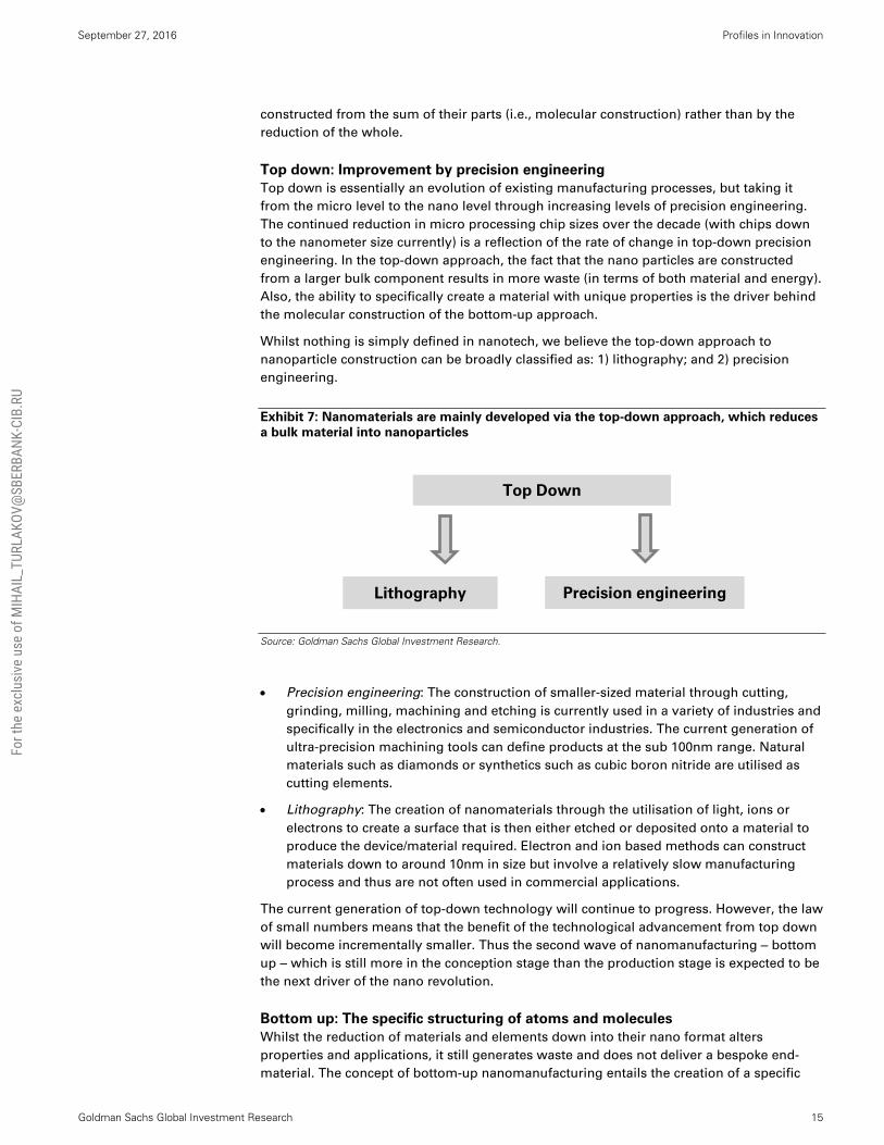
Top down: Improvement by precision engineering
Top down is essentially an evolution of existing manufacturing processes, but taking it
from the micro level to the nano level through increasing levels of precision engineering.
The continued reduction in micro processing chip sizes over the decade (with chips down
to the nanometer size currently) is a reflection of the rate of change in top-down precision
engineering. In the top-down approach, the fact that the nano particles are constructed
from a larger bulk component results in more waste (in terms of both material and energy).
Also, the ability to specifically create a material with unique properties is the driver behind
the molecular construction of the bottom-up approach.
Whilst nothing is simply defined in nanotech, we believe the top-down approach to
nanoparticle construction can be broadly classified as: 1) lithography; and 2) precision
engineering.
Exhibit 7: Nanomaterials are mainly developed via the top-down approach, which reduces
a bulk material into nanoparticles
Source: Goldman Sachs Global Investment Research.
Precision engineering: The construction of smaller-sized material through cutting,
grinding, milling, machining and etching is currently used in a variety of industries and
specifically in the electronics and semiconductor industries. The current generation of
ultra-precision machining tools can define products at the sub 100nm range. Natural
materials such as diamonds or synthetics such as cubic boron nitride are utilised as
cutting elements.
Lithography: The creation of nanomaterials through the utilisation of light, ions or
electrons to create a surface that is then either etched or deposited onto a material to
produce the device/material required. Electron and ion based methods can construct
materials down to around 10nm in size but involve a relatively slow manufacturing
process and thus are not often used in commercial applications.
The current generation of top-down technology will continue to progress. However, the law
of small numbers means that the benefit of the technological advancement from top down
will become incrementally smaller. Thus the second wave of nanomanufacturing ‒ bottom
up ‒ which is still more in the conception stage than the production stage is expected to be
the next driver of the nano revolution.
Bottom up: The specific structuring of atoms and molecules
Whilst the reduction of materials and elements down into their nano format alters
properties and applications, it still generates waste and does not deliver a bespoke end-
material. The concept of bottom-up nanomanufacturing entails the creation of a specific
Top Down
Lithography Precision engineering
For t
he e
xclu
sive
use
of M
IHAI
L_TU
RLAK
OV@
SBER
BANK
-CIB
.RU

September 27, 2016 Profiles in Innovation
Goldman Sachs Global Investment Research 16
structure using the atom or molecule as a building block for its construction. The material
is essentially created by the bespoke placement of atoms into a formation to create a
structure with defined and distinct properties. The bottom-up approach is still evolving
through the research phase with many industry experts believing that the approach is likely
to start to become a viable manufacturing process within the next 5-10 years.
Exhibit 8: The bottom-up approach is the potential future of nanotechnology
Source: Goldman Sachs Global Investment Research.
There are broadly three techniques for the bottom-up construction of nanomaterials;
Chemical synthesis (such as chemical vapor deposition – CVD): A process whereby
chemicals react to produce a nanomaterial that is deposited onto a thin film.
Positional assembly: An external force (energy) is exerted onto atoms and molecules
and they are forcibly shifted into a position to construct a desired material. Limited
waste would ensue, but the application of force/energy would remain required. The
construction of structures though positional assembly could make it possible to build
nano-bots and other nanoscale machines. However, although the creation of nano-
factories capable of churning out nanomaterials would appear to be possible; it is still
at this stage a scientific dream.
Self-assembly: Atoms arranging themselves in an ordered and engineered manner to
construct a pre-determined material. Given that the construction is at the atomic level,
there will be no waste and limited energy expenditure. Essentially, self-assembly has
the potential to be the ultimate “green” manufacturing process.
The bottom-up approach, specifically the creation of bespoke nano-scale materials,
machines and structures, is integral to the evolution of nano-manufacturing. The ability to
create custom, unique materials could help develop fields such as semiconducting,
nanomedicine (through drug delivery applications) and water filtration (via improved
catalysis).
Thus, although nanotech is now more focused on creating additive materials to enhance
existing applications, the next wave of nanomanufacturing could help solve some of the
key problems that an ever-industrializing world faces. Although nanotech may be
approaching its half century as a scientific field, it is only in its infancy as a manufacturing
process.
Bottom up
Chemical
synthesisSelf-assembly
Positional
assembly
For t
he e
xclu
sive
use
of M
IHAI
L_TU
RLAK
OV@
SBER
BANK
-CIB
.RU

September 27, 2016 Profiles in Innovation
Goldman Sachs Global Investment Research 17
The nanotech microscope evolution
Microscope: Derived from the Ancient Greek words mikrós (small) and skopeîn (to look).
Exhibit 9: Electron microscopes’ ability to view nano-objects has driven R&D in the field of nanotechnology Resolving power of microscopes
Source: Goldman Sachs Goldman Investment Research
The development of microscopes has come a long way since they were first used to discover microorganisms back in
in the 1600s. While optical microscopes have been the mainstay of imaging during this period, their advancement has
been limited by their inability to magnify and resolve images smaller than c.200nm (constrained by the wavelength of
light) and their limited depth of field (two-dimensional imaging).
This all changed in the 1930s through the invention of scanning electron microscopes (SEMs). Using electrons instead
of light, they made it possible to resolve features down to a few nanometers. The electron microscope, first developed
by German engineers Ernst Rusky and Max Knoll, uses a focused beam of electrons to probe a sample in a vacuumed
environment, and the electronic signal is processed to form an image, achieving magnifications of up to 1,000,000
times. Early progress in material science was mostly limited to studies of small particles, and during this time
microscopes could determine the size and shape of materials but not reveal their internal structure.
In 1982, the scanning tunneling microscope (STM) was invented by Gerd Binnig & Heinrich Rohrer in IBM’s Zurich
laboratory (they were later awarded the 1986 Nobel Prize in Physics for this invention). This was the precursor of
nanotech research as the STM was able to: (i) display three-dimensional images of samples down to an atomic level;
and (ii) allow for the manipulation of nanoscale particles and atoms to test for their various characteristics and
functionalities. However, a major drawback of the STM was its lack of ability to interact with non-conductive materials.
In 1986, the same inventors of the STM invented the atomic force microscope (AFM); the most-used nanoscale
microscope, given its ability to scan non-conductive samples. Originally used to image topography of surfaces, it is
also able to measure other characteristics of materials (electric and magnetic properties, friction and chemical
properties).
Today, electron microscopes are an indispensable tool for analyzing and constructing new nanomaterials. Further,
microscopes have recently been integrated to perform in-situ nanomaterial engineering and fabrication using
techniques such as: (i) nanomanipulation; (ii) electron beam nanolithography (using AFMs); and (iii) focused ion beam
techniques. Examples of products that have improved via these techniques include lithium-ion batteries,
nanomaterials and semiconductors.
For t
he e
xclu
sive
use
of M
IHAI
L_TU
RLAK
OV@
SBER
BANK
-CIB
.RU

September 27, 2016 Profiles in Innovation
Goldman Sachs Global Investment Research 18
Commercialising nanotechnology
The benefits of nanotech have long been recognised by governments and the private
sector. The National Nanotechnology Institute (NNI) is a US government agency focused
on nanotech R&D. The NNI was established in 2000 and since then has been a leader in the
field. Since its inception, the NNI has received almost US$20bn of government funding
with the 2017 budget set at US$1.4bn.
Exhibit 10: Total NNI funding
Source: CRS & NNI
Government funding is increasingly matched by spending from private equity and VC firms
as well as R&D spending from larger corporations. The OECD estimates that global R&D
spend on nanotech is in the order of US$26bn pa with the United States, Korea and Japan
all major contributors. Given that the data does not include regions such as China, the total
spend is likely to be significantly higher, in our view.
Exhibit 11: Japan, the US and Korea dominate nanotech
patents… % of nanotech patents by country (2015)
Exhibit 12: …with the number of patents a broad
reflection of R&D spend R&D spend in nanotech sector (2015)
Source: OECD, Goldman Sachs Global Investment Research.
Source: OECD, Goldman Sachs Global Investment Research
0
500
1,000
1,500
2,000
2,500
2001 2003 2005 2007 2009 2011 2013 2015E
US
$ m
n
Regular appropriations ARPA
0%
1%
2%
3%
4%
5%
6%
7%
8%
9%
10%
0
500
1,000
1,500
2,000
Un
ite
d S
tate
s
Ko
rea
Germ
an
y
Ja
pa
n
Fra
nce
Ru
ssia
Ita
ly
Be
lgiu
m
Me
xic
o
Sw
itze
rlan
d
Irela
nd
Cze
ch
Re
pu
bli
c
So
uth
Afr
ica
No
rway
De
nm
ark
US$
mn
Total nanotechnology R&D
expenditure,US$mn PPP
(LHS)
14,054 7,687
0
5
10
15
20
25
30
Ja
pa
n
Un
ited
Sta
tes
Ko
rea
EU
28
BR
IIC
S
Ch
ina
Ta
iwa
n
Germ
an
y
Fra
nce
Un
ite
d K
ing
do
m
Ca
na
da
Ne
the
rla
nd
s
Ita
ly
Sin
ga
po
re
Be
lgiu
m
Sw
itze
rla
nd
Ind
ia
Sp
ain%
of
Nan
ote
ch p
aten
ts g
loball
y
For t
he e
xclu
sive
use
of M
IHAI
L_TU
RLAK
OV@
SBER
BANK
-CIB
.RU

September 27, 2016 Profiles in Innovation
Goldman Sachs Global Investment Research 19
According to OECD data, there are around 15,000 firms exposed to nanotech ‒ as
manufacturers or via overlaps their operations have with nanotech. Of those firms, almost
1,000 say they are dedicated solely to the field of nanotech. The range of R&D is massively
broad given the scope of what nanotech entails – for instance, graphene research classifies
as a subset of nanotech, and as such the spend may not represent direct investment in the
research, development and propagation of nanotech and nanomanufacturing. Our analysis
indicates that, to date, most of the commercial aspects of nanotech have been focused on
additive materials, which alter and/or enhance existing properties of materials. For
example, housing paints with nano-particles such as titanium oxide (TiO2), are considered
nanotech products, and this would also be the case for a tennis racket with a slight additive
of graphene (though whether the addition of the nano-material improves the product
quality is another matter).
Additives – the here and now of nanotechnology
Spurred on by the never-ending demand for product improvements, companies are
increasingly looking to nanotech as a way to gain a decisive edge. It remains difficult to
determine how much these products are actually improved by nanotech, and how much is
a marketing strategy. Using The Project on Emerging Nanotechnologies database of
Consumer Product Inventory, we can identify 1,944 distinct registered applications of
nanotech. The data may not be truly reflective of the amount of applications as some
companies may not promote the use of nanotech in their products and some may
overstate the nanotech component. However, we believe it does provide a reasonable
breakdown of nanotech applications from an additive perspective.
Some market research has suggested that nanotech could be a US$1trn market by 2030.
However, we caution that this reflects the dollar value of the end-products that include
nano-materials and is not a reflection of the value or revenue that actual nanoparticles
deliver.
Exhibit 13: The United States is a leader in nano product
development…
Exhibit 14: …with silver (a known-known) dominating as
the key nano element, and graphene with two
applications only thus far
Source: The Project on Emerging Nanotechnologies, Goldman Sachs Global Investment Research
Source: The Project on Emerging Nanotechnologies, Goldman Sachs Global Investment Research
0
100
200
300
400
500
600
700
800
'Nan
o'
pro
du
cts
by
cou
ntr
y
050
100150200250300350400450500
Top 1
0 '
nano'
mat
eri
als
Most of the commercial aspects of nanotech have been focused on additive materials, which alter and/or enhance existing properties of materials.
For t
he e
xclu
sive
use
of M
IHAI
L_TU
RLAK
OV@
SBER
BANK
-CIB
.RU

September 27, 2016 Profiles in Innovation
Goldman Sachs Global Investment Research 20
Exhibit 15: …health and fitness (personal care) is the top
category for nano applications…
Exhibit 16: …with antimicrobial protection (sunscreen,
cosmetics, etc.) the lead nano function
Source: The Project on Emerging Nanotechnologies, Goldman Sachs Global Investment Research
Source: The Project on Emerging Nanotechnologies, Goldman Sachs Global Investment Research.
Other technological advancements utilising nanotech include:
Nanocomposites: The inclusion of nanoparticles into a larger sample material
(generally accounting for <5% of the mass of the main material), which enhances the
physical properties of the resulting naoncomposite. Can be found in fabrics, solar cells,
coatings, super capacitors, etc.
Nano-electrodes: They perform similar to normal electrodes but on a nano scale. The
high surface to volume area of the nanoparticles lead to larger electrode contact areas
and thus enhance mass transport. The faster transport of the electrons results in
enhanced electrical and ionic conductivity – improving charge times is one example.
Lithium-ion batteries, supercapacitors, fuel cells and solar cells have all seen improved
energy performance due to nano-electrodes.
Nano coatings: Used in a variety of applications where nanotech can provide a
coating or film that improves and alters the reactivity of the material it coats. This
includes coatings on cars to reduce the need to wax, films in paints to improve
washability, and utilisation in solar cells to enhance the manufacturing of photovoltaic
cells.
Nano-products are clearly evolving. The next generation of products (utilising the bottom-
up approach to nanomanufacturing) are becoming more defined for specific tasks, and will
likely start to be commercialised in coming years. In the case studies on pages 50-63, we
examine several applications where we believe nanomanufacturing will have a significant
impact on the current industry status quo ‒ including boosting potable water availability in
the emerging world and improving the delivery of cancer drugs.
0
100
200
300
400
500
600
700
800
900
1000
'Nan
o'
pro
duct
s b
y ca
teg
ory
050
100150200250300350400450
Top
10
'nan
o'
funct
ions
For t
he e
xclu
sive
use
of M
IHAI
L_TU
RLAK
OV@
SBER
BANK
-CIB
.RU

September 27, 2016 Profiles in Innovation
Goldman Sachs Global Investment Research 21
KEY APPLICATIONS
GRAPHENE
History: Still relatively young; first isolated in 2004
Benefits: Strength, conductivity, transparency, weight and unique 2D
structure
Commercialisation: Slowly beginning to ramp up, cost reduction is key
Potential applications: Mobile technology, water filtration, foldable display
technology, batteries and energy storage, composite materials, sensors, paints
and coatings, printing and packaging
Select company exposure: End-consumers such as Samsung, Apple, and
LG will be ultimate users of graphene in conductors and mobile technology
applications. Lockheed Martin is leader in water filtration development.
Producers of graphene such as Graphena, Dongxu Optoelectronic Technology
and Graphene Laboratories are all looking to commercialise graphene
manufacturing.
For t
he e
xclu
sive
use
of M
IHAI
L_TU
RLAK
OV@
SBER
BANK
-CIB
.RU

September 27, 2016 Profiles in Innovation
Goldman Sachs Global Investment Research 22
Graphene: The carbon source for the next industrial revolution
From coal to graphene, carbon has been ever-present in the evolution of manufacturing.
Just as coal was a driving force behind the development and progression of the industrial
revolution, graphene has the potential to drive another phase of change. Graphene’s
strength (it is 300 times stronger than steel), conductivity (its electrical current density is
106 greater than copper’s), and transparency make it unique and well-suited for use in a
myriad of end-market opportunities and products.
Whilst graphene is now mainly used in small amounts as an additive to enhance the
properties of other materials, it has the potential to play a key role in the rapid
development and structural change of industries ‒ due to its use in carbon nanotubes,
flexible semiconductors, water filtration, and much more.
Graphene could revolutionize audio visual technology via its use in foldable displays and
devices and with non-traditional surfaces (such as windows) used as visual displays.
Given that graphene was only isolated in 2004, its potential as an enabler of new
technology remain embryotic, but with companies such as Samsung and LG continually
adding patents around graphene, the applications and end-markets for the material look
set to ramp up sharply.
The history of graphene and its benefits
The differentiator of graphene from other carbon allotropes, such as graphite, is its size.
Graphene is essentially a 2D (single layer) material and in its purest form it is only a single
carbon atom thick. Its nearest cousin, graphite (the current material de jour for its use as an
anode in lithium-ion batteries) has a layered planar structure. In layman’s terms, an
effective way to visualize the difference between graphite and graphene is to think of a
deck of cards. Graphite is two to three decks of cards stacked on top of one another.
Graphene is a single card. This unique structure makes graphene much stronger than
graphite.
Graphene was first conceptualized in the 1940s. However it was not until microscope
technology (mainly the development of transmission electron microscopes in the 1960s
and 1970s) allowed the first glimpses into its physical. The first attempts to isolate
graphene were conducted in the 1990s and early 2000s; they focused on isolating graphene
sheets (essentially graphite) with no reported success in delivering graphene in less than
50 layers thick before 2004.
Sir Andre Geim and Sir Kostya Novoselov isolated graphene in 2004, and received a Nobel
Prize in 2010 for “for groundbreaking experiments regarding the two-dimensional material
graphene”. The isolation of individual layers of graphene, and the exceptional properties it
delivers, started a “carbon-rush” into the research and development of the material.
Since then, graphene’s viral acceleration into the mainstream has resulted in more than
32,000 patent applications in the past five years and nearly 10,000 research papers
published on it annually.
Graphene is a single atomic layer of graphite arranged in a hexagonal lattice, and is the world’s first 2D (single layer) material.
Allotrope: one form type in which an element can occur.
For t
he e
xclu
sive
use
of M
IHAI
L_TU
RLAK
OV@
SBER
BANK
-CIB
.RU

September 27, 2016 Profiles in Innovation
Goldman Sachs Global Investment Research 23
Exhibit 17: Recent years have seen an increase in the
number of patents filed relating to graphene…
Exhibit 18: …with China emerging as a leader in
graphene technology, followed by Korea.
Source: SciVal
Source: World Intellectual Property Organization
The buckyball – Generation X’s cautionary tale on graphene
The buckyball provides a cautionary tale for the hype around graphene. Buckyballs – or more formally
Buckminsterfullerene – is a form of fullerene, which is a molecule of carbon and thus a close cousin to graphene. The
buckyball is a spherical fullerene, with a broad resemblance to a soccer ball containing 60 carbon atoms.
Whilst spherical fullerene had been theorized about as early as the 1960s it was not until the mid-1980s that the
buckyball was discovered using laser evaporation of graphite.
In 1986, the early pioneers of Buckminsterfullerene (like those of graphene) were awarded a Nobel Prize. The buckyball’s
properties of large internal space inside the molecule, its bond structure and superconductivity made it a matter of
interest for scientists looking to develop applications including hydrogen storage and fuel cells, a trap for free radicals
that can reduce allergic reactions, an anti-oxidant to fight multiple sclerosis and a building block for the creation of
carbon nanotubes.
Sound familiar?
Despite the buckyball being the wonder of the AMs space in the 1980s and 1990s, not a single application using the
buckyball has been commercialised. Interestingly, graphene is now being proposed as a possible solution for many of
the applications that buckyballs were once thought to be useful for.
Whilst the lack of commercialisation of graphene’s carbon cousin is not in itself a death knell for the development of
graphene given their different atomic characteristics, it is certainly a cautionary tale on how hype does not always
translate into profit pools.
Exhibit 19: A buckyball structure
Exhibit 20: Buckyball patents peaked 5 years after 500
patents were lodged and have been on a decline since YoY patents changes in years after first 500 patents lodged
Source: Goldman Sachs Global Investment Research.
Source: WIPO and Goldman Sachs Global Investment Research
18%
27%
42%
74%78%
60%
37%
45%
11%
0%
10%
20%
30%
40%
50%
60%
70%
80%
90%
0
2000
4000
6000
8000
10000
12000
2006 2007 2008 2009 2010 2011 2012 2013 2014 2015
Published Patents (Graphene, by year, LHS) % yoy growth (RHS)
0%
10%
20%
30%
40%
50%
2006 2007 2008 2009 2010 2011 2012 2013 2014 2015
US as % total China as % total Korea as % total
-20%
-10%
0%
10%
20%
30%
40%
50%
60%
70%
80%
90%
1 2 3 4 5 6 7 8 9 10
YoY
Pate
nt c
hang
e
Year since 500 Patents lodged
Buckyballs Graphene
For t
he e
xclu
sive
use
of M
IHAI
L_TU
RLAK
OV@
SBER
BANK
-CIB
.RU

September 27, 2016 Profiles in Innovation
Goldman Sachs Global Investment Research 24
The benefits of graphene
The attractions of graphene are its properties of strength, conductivity and transparency.
Each benefit in isolation provides inherently better properties than existing materials in
commercial consumption:
Strength: 300x stronger than steel
Conductivity: Electrical current density 106 greater than copper
Transparency: Given its single atomic thickness, sheets of graphene are transparent.
The combination of all three properties makes graphene unique in the material science
field.
Exhibit 21: Graphene a miracle material found in a simple form Comparison of different materials
Source: Company data, Goldman Sachs Global Investment Research.
Almost 25% of all patents that have been filed globally for graphene relate to
semiconductor technology. The commercial impact and subsequent utilisation in semi-
conductors is highlighted by Samsung and Semiconductor Energy Laboratory Corporation
of Japan being the two largest filers of patents with almost 1,000 patents each (2.3% of
total patents filed).
On a country level, Japan and Korea are leading the charge to commercialise graphene,
but China is catching up quickly, accounting for almost 30% of all patent applications in
2015. Government funding and policies coupled with world-class academic institutes and
research is propelling China to the forefront of graphene research. China’s five-year plan
for 2006-2010 tripled nanotech funding, highlighting the importance of cutting-edge
technology and materials to China’s vast manufacturing base.
Patent numbers have been rising since 2006, and momentum is growing, but graphene has
still yet to crack the commercial conundrum. Graphene’s strength of having a vast array of
applicability may also be its Achilles’ heel, with researchers taking a shotgun approach to
idea generation and thereby slowing down the economic commercialisation process. The
range of material applications for graphene includes semiconductors, water filtration,
edible packaging, carbon nanotubes and energy storage.
The fact that semiconductors are the single-biggest source of patents (and thus by default
research) for graphene is a reflection of graphene’s properties and the scarcity of existing
conductor materials. Currently indium tin oxide (ITO) is the main material used in
semiconductors. ITO’s properties of electrical conductivity, heat reflection and most
importantly transparency make it a perfect conducting film for the touchscreen display
revolution. However, ITO has a rather finite reserve life with our analysis suggesting that
Graphene Metal only Metal + plastic Alumina + plastic Graphite + plastic Graphite sheet
Conductivity Good Excellent Good Poor Poor Good
Additive amount Small N/A Small Large Large N/A
Strength Good Excellent Good Poor Poor Good
Weight Light Heavy Heavy Heavy Light Light
Insulation property Good Poor Poor Good Poor Poor
Cost Can be low High High Low High High
Workability Good Poor Poor Poor Poor Poor
Almost 25% of all patents that have been filed globally for graphene relate to semiconductor technology.
For t
he e
xclu
sive
use
of M
IHAI
L_TU
RLAK
OV@
SBER
BANK
-CIB
.RU

September 27, 2016 Profiles in Innovation
Goldman Sachs Global Investment Research 25
there is only around 8-10 years of global indium reserves left. Thus graphene, with its
similar properties to ITO and its almost endless supply, could be the perfect replacement
material – if its cost of “construction” can be reduced to become economically viable.
Exhibit 22: Graphene patents by country of application Exhibit 23: Graphene patents by end-product application
Source: World Intellectual Property Organization
Source: World Intellectual Property Organization
Whilst semiconductors is likely to be the main focus of graphene, potential end-
applications for graphene are almost endless, but we acknowledge that the key to
graphene’s success lies with its ability to dislodge existing materials and disrupt the status
quo. On this theme, a few factors are key to crystallising widespread commercial uptake:
Reducing costs of production.
Developing a reputation of high product quality to drive substitution.
Educating the masses to view graphene as value-enhancing rather than as a cost.
Whilst the here and now of graphene is still at an embryonic stage, its potential remains
immense, in our view. Just like plastics in the 1920s and 1930s, graphene is waiting for a
“killer app” to kick off exponential demand growth. WWII provided the catalysts to drive
plastic demand (given limited other raw materials). Global conflict is unlikely to be the
game changer for graphene, but the scarcity of critical global resources (ITO, clean water)
coupled with the desire of a wealthier middle class to stay healthy (nano-medicine) will be
two important drivers.
USA
44%
Other
21%
China
19%
EU
6%
Korea
6%
Japan
2%
Canada
2%UK
0%
Semi-
conductor
25%Compounds
18%
Batteries
13%
Nano particle
technology
8%
Catalysis
6% Other
30%
The key to graphene’s success lies with its ability to dislodge existing materials and disrupt the status quo.
For t
he e
xclu
sive
use
of M
IHAI
L_TU
RLAK
OV@
SBER
BANK
-CIB
.RU

September 27, 2016 Profiles in Innovation
Goldman Sachs Global Investment Research 26
Where’s my Indium?
Indium is a silvery-white metal that is associated with zinc, copper and tin. Indium is typically a significantly minor
component of the ore assemblages with approximate concentration levels of around 50ppm. Indium is principally a
byproduct of the electrolytic refining of zinc ores.
Over 70% of indium is consumed as indium-tin oxide (ITO) for liquid crystal displays. ITO’s properties of electrical
conductivity, heat reflection and, most importantly, transparency make it a perfect conducting film for the touchscreen
display revolution.
Although reserves of indium are not classified, we can approximate off zinc reserves that there is around 10kt of indium
reserves globally with about 20% of that within China. Indium supply is a combination of primary supply from mines,
along with recycled indium at a rate of about 40/60 primary/recycled split.
On current demand levels, we estimate there is around 10-12 years of known indium reserves left globally.
Assuming an 8% CAGR for demand, we forecast that by 2019 indium supply will not be enough to meet demand. More
importantly, indium reserves will be down to five years, impacting surety of supply for producers. Consequently, the
need to replace ITO with other conducting material is both a financial and a security of supply issue.
Exhibit 24: Current indium reserves are around 10kt,
which represents just over 10 years of supply Indium reserves are based on global zinc reserves and
assume a 50ppm content level of indium among the zinc ore
Exhibit 25: By the end of the decade, demand for indium
is set to surpass supply Indium mine supply/demand balance
Note: Demand assumes a 8% CAGR and mine supply growth in line with zinc production levels
Source: USGS, Goldman Sachs Global Investment Research.
Source: Company data, USGS, Goldman Sachs Global Investment Research.
Indium Reserves (t) % of world supply
USA 550 5%
Australia 3150 31%
Bolivia 250 2%
Canada 300 3%
China 1900 19%
India 500 5%
Ireland 50 0%
Kazakhstan 200 2%
Mexico 750 7%
Peru 1250 12%
Other 1300 13%
Total 10200 100%
0
500
1,000
1,500
2,000
2,500
3,000
tonn
es
Mine supply Recycled supply Demand
For t
he e
xclu
sive
use
of M
IHAI
L_TU
RLAK
OV@
SBER
BANK
-CIB
.RU

September 27, 2016 Profiles in Innovation
Goldman Sachs Global Investment Research 27
Graphene manufacturing processes
The manufacturing graphene on a commercial scale is not as straightforward. There are
three main ways to produce graphene in commercial quantities:
1. Chemical vapour deposition (CVD) – the most common and expensive method, it
produces high-quality sheets of graphene. It involves extracting carbon atoms from a
carbon-rich source by reducing and depositing gaseous reactants onto a substrate to
isolate carbon atoms and graphene.
2. Graphene powder and flakes – this involves exfoliating plastics and is used to produce
high-quality thermal plastics.
3. Graphene oxide – graphite is treated with strong oxidisers like sulfuric acid in a redox
reaction. The quality of graphene produced via this process is not very high.
Exhibit 26: Exfoliation is a relatively cheaper method to
produce graphene Comparison of different graphene production methods
Exhibit 27: Application areas have huge potential
Source: Graphene Platform Corporation, Goldman Sachs Global Investment Research.
Source: Graphene Platform Corporation, Goldman Sachs Global Investment Research.
Cost reduction the key for commercial success
The cost-consumption arbitrage for graphene still has a long way to go. Whilst the past
decade has seen the production of graphene move from a cottage industry to a more
commercial focus, it is still not a mass-production process.
Cost progression has been rapid. We estimate unit costs of graphene powder production
were around US$100/g in 2013, falling to around US$10/g presently. However, costs need
to fall further to <US$1/g to be competitive and provide a viable substitution alternative for
other materials (such as the addition carbon black in plastics). Given a 90% reduction in
costs in the past three years, we believe the commercial construction of graphene at sub
US$1/g is a given.
The ability of cost-effective graphene to impact an industry is significant – take carbon
black for example. Carbon black is most widely used as reinforcement in tires, and it
accounts for c.25% of tire weight, (about 9-10kg for a 16-17-inch tire). According to Japan’s
Ministry of Economy, Trade and Industry (METI), the price of carbon black was c.US$1.5/kg
in 2015. It is thought that graphene will be able to replace carbon black in plastics while
amounting for only 1%-2% of the product content– reducing per-content usage by a
significant amount, while enhancing durability and grip, and reducing rolling resistance.
SyntheticHigh Cost
High Quality
Value Added Applications
CVD
Epitaxial Growth on SiC
Micromechanical Exfloliation
ExfoliationLow Cost
Low Purity
Mass Production
Chemical Reduction of Graphene Oxide
Ultrasound
Liquid Phase Exfoliation
For t
he e
xclu
sive
use
of M
IHAI
L_TU
RLAK
OV@
SBER
BANK
-CIB
.RU

September 27, 2016 Profiles in Innovation
Goldman Sachs Global Investment Research 28
This would mean that graphene would become competitive vs. carbon black if it is sold at
around US$20-30/kg.
Exhibit 28: Graphene price of US$20-30/kg would make it competitive as a tire additive Pricing simulation for tire reinforcement (carbon black vs. graphene)
Source: METI, Goldman Sachs Global Investment Research.
The history of carbon fiber resonates well with the analysis above. The early stage of
carbon fiber demand was solely driven by military use, mainly in the United States and the
United Kingdom. When the Japanese manufacturers became successful in the commercial
production of carbon fiber in the early 1970s, companies searched for consumer-facing
applications, but for a long time demand was limited to niche sports categories such as
golf shafts, fishing rods, and tennis rackets. It took nearly 30 years until the industry saw a
meaningful pick-up in global carbon fiber demand, which was driven by industrial
applications. By the early 2000s, prices for general-industrial grade carbon fiber had come
down to US$3,000 per kilogram, from US$9,000 back in the late 1980s.
However, while the development of carbon fiber was relatively slow, we believe there are
several reasons why graphene has the potential to evolve in a more super-charged
manner:
1. Computing and general scientific technology is now much more advanced than in
the 1980s and 1990s and should enable the scientific development of graphene to
proceed much faster than was the case with carbon fiber.
2. The desire of consumers for smaller, faster, and lighter products provides the pull
factor for producers to utilise graphene in their R&D programs and product
development.
3. The pick-up in carbon fiber demand in the early 2000s coincided with higher oil
prices and the global push toward environmental protection. Graphene properties
are exceptionally environmentally friendly.
Carbon black Graphene
2.5 0.2
Total cost as tire reinforcement
3.8 3.8 USD
Tire weight 10 kg
kg
Unit price 1.5 25.0 USD/kg
Total weight needed
% of tire weight 25.0% 1.5%
For t
he e
xclu
sive
use
of M
IHAI
L_TU
RLAK
OV@
SBER
BANK
-CIB
.RU

September 27, 2016 Profiles in Innovation
Goldman Sachs Global Investment Research 29
Exhibit 29: Global demand for carbon fiber took off as a result of lower prices Historical development for global carbon fiber demand and prices for general industrial-grade carbon fiber
Source: Toray Industries, Nikkei Shimbun, Goldman Sachs Global Investment Research
Potential applications for graphene
Graphene’s superior strength-to-weight ratio, electric and thermal conductivity, durability,
transparency, elasticity and impermeability mean that potential applications could be
massive and disruptive to some of the incumbent materials and industries. Let us take a
look at some areas where graphene could be used.
As mentioned before, the current global market size for graphene is estimated to be under
US$50mn, with limited commercial applications such as tennis rackets, battery straps and
oilfield chemicals. Below are some examples of potential areas of graphene applications
that we believe hold significant potential.
Foldable display (wearables): Bendable smartphones are in the R&D programs of many of
the world’s phone manufacturers. Graphene can be used as a transparent electrode placed
between titanium oxide (TiO2) and conducting polymer layers in OLED displays. On June 7,
2016, Bloomberg reported that Samsung is close to selling a phones with 5-inch bendable
screens, possibly in 2017. China’s tech-startup, Moxi Group, surprised the world when it
showcased a flexible smartphone at a trade show in China earlier this year.
Batteries and energy storage: Although lithium-ion batteries are in the spotlight with
Tesla’s Gigafactory and the potential rise in the global electric vehicle (EV) market,
graphene batteries reportedly charge much more quickly and hold power for longer.
Graphenano, a Spain-based company, has tied up with China’s Chint Group, a power
transmission and distribution company, to develop graphene polymer batteries that would
significantly increase cruising distance for EVs. Although much skepticism remains about
graphene’s superiority over incumbent lithium-ion batteries, implications for the EV
industry could be massive (especially for companies like Tesla) if graphene batteries can
make a commercial debut.
● Fishing rod● Artificial satellite● Secondary structural material for Boeing 757/767
● Tennis racket● Golf shaft● Primary structural material for Airbus 320
● General industrial-use applications (energy, transportation, etc)● Primary structural material for Boeing 777
● Primary structural material for Airbus 380 & Boeing 787● Windmill blade● Automotive-related use
1971-1983Introductory period
1984-1993Growing period
1994-2003Expansionary period
2004 onwardsDemand acceleration period
0
1,000
2,000
3,000
4,000
5,000
6,000
7,000
8,000
9,000
10,000
0
10
20
30
40
50
60
70
1970
1971
1972
1973
1974
1975
1976
1977
1978
1979
1980
1981
1982
1983
1984
1985
1986
1987
1988
1989
1990
1991
1992
1993
1994
1995
1996
1997
1998
1999
2000
2001
2002
2003
2004
2005
2006
2007
2008
2009
2010
2011
2012
2013
2014
2015
General industrial
Aerospace
Sporting goods
(000 tonne) (JPY/kg)
Price (rhs)
For t
he e
xclu
sive
use
of M
IHAI
L_TU
RLAK
OV@
SBER
BANK
-CIB
.RU

September 27, 2016 Profiles in Innovation
Goldman Sachs Global Investment Research 30
Composite materials: Adding graphene to a composite material is said to be one of the
easiest ways to enjoy the superior properties of graphene as it enhances the properties of
the existing material. For instance, Haydale Graphene Industries a UK-based public
company that specializes in developing and functionalizing graphene, recently announced
the launch of graphene-enhanced carbon fiber prepreg (pre-impregnated product), which is
capable of faster composite part production (reducing process cycle times), enduring
higher temperatures, and high-accuracy tooling. The addition of graphene is also said to
double the strength of epoxy resin, which is typically used in carbo fiber composites. This
could be a game changer and could facilitate adoption of carbon fiber composites into
wider applications.
Sensors: Graphene could be used in high-performance sensors as its large surface-to-
volume ratio and bulk-less properties make it very well-suited for sensor functions.
Graphene has the potential to replace silicon as it could exhibit superior electron properties
while enabling sensors to be smaller and lighter. Applications could be widespread,
including biosensors, gas sensors, PH sensors, and more. In July 2015, Germany-based
Bosch successfully created a graphene-based magnetic sensor that is 100 times more
sensitive (i.e., required less power and footprint requirements) than the traditional silicon-
based sensor, although the company thinks it might take another 5-10 years for graphene-
base sensors to become commercially viable.
Paints and coatings, printing and packaging: Conductive printing and packaging is another
potentially promising area of graphene use. A UK-based technology company, Novalia,
together with researchers at University of Cambridge, recently developed a graphene-
based conductive ink that could be used on a large-scale commercial printing press at high
speed – a development that could potentially replace silver. A successful commercialization
of graphene ink could mean cheaper printable electronics, but would also open up
potential applications for smart packaging and disposable sensors.
For t
he e
xclu
sive
use
of M
IHAI
L_TU
RLAK
OV@
SBER
BANK
-CIB
.RU

September 27, 2016 Profiles in Innovation
Goldman Sachs Global Investment Research 31
OLEDs: Bending the future
KEY APPLICATIONS
OLEDs
History: Modern OLEDs were developed by Eastman Kodak in 1987
Benefits: Better contrast ratios, colour schemes and saturation, flexible and
bendable properties
Commercialisation: Present-day applications already attractive, mobile
(smartphones and tablets) are already in the early stages of adoption
Potential applications: Smartphones, tablets, TVs, revolutionizing what is
classified as audio-visual equipment (turning a window into a TV display)
Select company exposure: Samsung, Apple, LG, Universal Display, Applied
Materials, ULVAC
For t
he e
xclu
sive
use
of M
IHAI
L_TU
RLAK
OV@
SBER
BANK
-CIB
.RU

September 27, 2016 Profiles in Innovation
Goldman Sachs Global Investment Research 32
OLEDs: Bending the future
If the term organic light-emitting diodes (OLEDs) seems more familiar than the other AMs
we discuss in this report, that is likely due to the mass branding and marketing of the term
in products such as mobile devices and TVs. OLEDs have the potential to leverage and
collaborate with both graphene and nanotech to fundamentally shift the world’s mobile
technology landscape.
The flexible nature of OLEDs gives them the ability to challenge what society perceives as
audio-visual equipment. TVs remain a separate and distinct piece of furniture in our
households. OLEDs have the ability to make a window or mirror or fish tank into something
that can project a visual message.
The ability to utilise buildings, windows, and shop fronts as new mediums for commercial
messages could change how we advertise and interact in our daily shopping experiences.
Much as the mobile phone continues to challenge and alter our audio communication
trends, OLEDs have the potential to drastically alter our visual communication
consumption.
Exhibit 30: Commercial crystallisation lifecycle
Exhibit 31: AMs collaborate further to facilitate the ever
demanding global consumer
Source: Goldman Sachs Global Investment Research.
Source: Goldman Sachs Global Investment Research.
A brief history of OLEDs and why they matter
OLEDs utilise the scientific property of electroluminescence, where a material emits light
when an electric current is sent through it. OLEDs use a flat light-emitting technology,
made by placing a series of organic thin films between two conductors.
The basic structure of an OLED includes a cathode (which injects electrons), an emissive
layer, and an anode (which removes electrons). Modern OLED devices use multiple layers
in order to boost efficiency, but the basic functionality remains the same.
Paradigm Shift
Mind Share
Economies of Scale
Substitution
Mass Adoption
For t
he e
xclu
sive
use
of M
IHAI
L_TU
RLAK
OV@
SBER
BANK
-CIB
.RU

September 27, 2016 Profiles in Innovation
Goldman Sachs Global Investment Research 33
Exhibit 32: Organic polymers usually make up the
emissive and conducive layers in OLEDs Simplified OLED components
Exhibit 33: Diagram of the structure of an OLED
Source: Goldman Sachs Global Investment Research.
Source: Goldman Sachs Global Investment Research.
While light emitting diodes (LEDs) have been around for over 50 years, OLEDs are a more
recent development in the AM space with the most significant advances in OLED
technology being made in the late 1980s.
Following those advances, the pace and progress of OLED development increased
markedly over the next decade. However, it was not until the late 1990s that the first
commercial OLED-based products began to reach the market, led by the Pioneer
Corporation’s passive matrix OLED (PMOLE) display for car audio in 1997. Fast forward
another decade and in 2007 Samsung Mobile Display released the first commercial active
matrix OLED (AMOLED) display. AMOLED is now the technology currently used in virtually
all OLED displays found in portable electronics and larger area flat-panel displays.
OLEDs have a number of properties that are superior to those of more established
technologies like LCDs and LEDs. LEDs are solid-state devices that emit light via the
movement of electrons through a semiconductor but are too big to be appropriate for use
as pixels in TVs. As such, they are actually used as backlights for LCD TVs. A key
differentiator for OLEDs is that their structure enables their organic compounds to light up
when electricity is transmitted through them. As a result, OLEDs are small and flexible
enough to serve as pixels in OLED TVs.
When used in mobile devices, OLED screens are distinctly better than traditional LCD
displays in terms of contrast ratios, colour schemes and colour saturation ‒ not to mention
their flexible and bendable properties.
Exhibit 34: Key advantages and disadvantages of OLEDs vs. LCDs
Source: DisplayMate, IHS, Goldman Sachs Global Investment Research.
Substrate
Anode
Conducive Layer
Emissive Layer
Cathode
Advantages of OLED versus LCD Disadvantages of OLED versus LCDThinner size as backlight is not required Higher per-unit production costsLighter Lower production yieldSmaller bezel Lower life spanWider viewing angles Unwanted burn-in of imagesMore vibrant display, deeper black, and vivid colorsBetter color reproductionFaster response timeHigher peak brightness
For t
he e
xclu
sive
use
of M
IHAI
L_TU
RLAK
OV@
SBER
BANK
-CIB
.RU

September 27, 2016 Profiles in Innovation
Goldman Sachs Global Investment Research 34
The hype: Present-day applications already attractive
Samsung, the global leader in smartphones (23% market share) uses OLEDs in their
flagship products, which has curved edges, and the ability to be tailored by the consumer
in terms of functionality.
Exhibit 35: The potential of flexible phones is vast... Flexible OLED phone indicative image
Exhibit 36: ...with flexible OLED technology being used in
mainstream phone models to create curved edges
Source: Goldman Sachs Global Investment Research.
Source: Goldman Sachs Global Investment Research.
We believe this is only the beginning, however, with flexible mobile technology having the
potential to drive change and consolidation in the mobile industry, i.e. in smartphones,
tablets, smartwatches. Samsung is at the forefront of this, having filed a number of patents
for an assortment of digital devices that include scrollable, tab style, and bendable features.
With the leading mobile innovators filing patents for a variety of modern applications (e.g.
Samsung for both scrollable and foldable smartphones), the profit pools and growth in
TAMs are potentially mind-boggling.
Having discussed the potential for OLEDs to transform the mobile landscape, it is
important to note that present-day applications are still highly commercially attractive; we
estimate a total addressable market of c.US$25bn by 2018.
Exhibit 37: Current mobile technology applications are the main demand drivers for OLED
technology OLED applications
Source: Goldman Sachs Global Investment Research.
Mobile
• Samsung clear market leader
• Cost of producing OLEDs on par with LCDs
TV
• TV market currently in an ex-growth phase
• Quantum dots could make OLEDs redundant
Lighting
• Energy efficient and environmentally friendly
• Potential to power cities globally
For t
he e
xclu
sive
use
of M
IHAI
L_TU
RLAK
OV@
SBER
BANK
-CIB
.RU

September 27, 2016 Profiles in Innovation
Goldman Sachs Global Investment Research 35
The promise: Mobile technology, all roads lead to OLEDs
Mobile devices (smartphones and tablets) are already in the early stages of OLED adoption,
with the better quality and increased longevity of OLEDs being integral to the disruption of
traditional LCD screens. In our view, there will be a transcendent structural shift to OLEDs
from LCDs within the next three to five years. We note that Samsung Display is currently
the only company mass-producing OLED-based screens; however, there are a growing
number of Chinese manufacturers trying to enter the space (Huawei, Lenovo, Xuamei).
Exhibit 38: Samsung dominates the global mobile AM OLED market Small/medium AM OLED global market share
Source: IHS
Smartphones are already integral to modern society (c.90% penetration), and are set to
become even more important to our personal Internet of Things as they become a one-stop
shop for wallets, payments, wearable hubs, and remotes connecting all aspects of our lives.
99% 97% 95%
0%
10%
20%
30%
40%
50%
60%
70%
80%
90%
100%
2013 2014 2015
Samsung Display LG Display EverDisplay Sony eMagin AUO
For t
he e
xclu
sive
use
of M
IHAI
L_TU
RLAK
OV@
SBER
BANK
-CIB
.RU

September 27, 2016 Profiles in Innovation
Goldman Sachs Global Investment Research 36
Exhibit 39: We expect emerging markets to drive
smartphone growth Smartphone penetration as % of total handset shipments by
region
Exhibit 40: Smartphone penetration approaching 90% Smartphone shipments (mn) and as % of total mobile
shipments
Source: Gartner, Goldman Sachs Global Investment Research.
Source: Gartner, Goldman Sachs Global Investment Research.
Samsung and Apple (combined 39% market share) have been the dominant smartphone
vendors over the last five years. However, both have lost share from their peaks (Samsung
at 30%/31% in 2012/13 and Apple at 19%/20% in 2011/12) primarily because of the mix shift
from mature to emerging markets, where new low-priced Chinese vendors have gained
traction. Indeed, the next three biggest smartphone manufacturers are all Chinese vendors:
Huawei (over 7%), Lenovo (5%, including acquisition of Motorola) and Xiaomi (5%).
Exhibit 41: Samsung is the global smartphone leader... Smartphone volume share (%), Global, 2015
Exhibit 42: …but Apple has a much bigger lead in the USSmartphone volume share (%), US, TTM (4Q14 to 3Q15)
Source: Gartner
Source: Gartner
A clear sign of the disruptive nature of OLED screens can be seen by the recently
negotiated US$2.6bn agreement whereby Samsung will supply Apple with 100mn 5.5-inch
OLED display units from 2017. We expect this agreement to expand to all sizes of iPhones
Samsung, 23%
Apple, 16%
Huawei, 7%
Lenovo+Motorola,
5%Xiaomi,
5%
LGElectronics
, 3%
Others, 41%
Apple, 40%
Samsung, 22%
LG Electronics
, 13%
ZTE, 7%
Lenovo+Motorola,
4%
Others, 14%
For t
he e
xclu
sive
use
of M
IHAI
L_TU
RLAK
OV@
SBER
BANK
-CIB
.RU
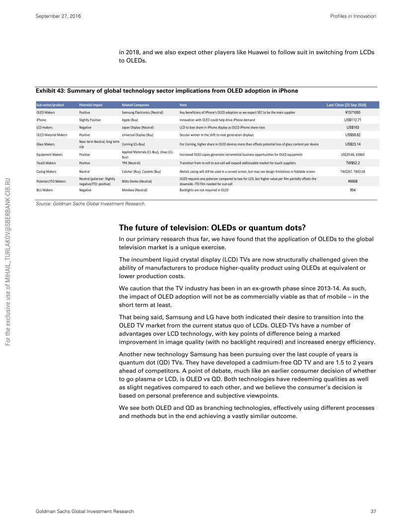
September 27, 2016 Profiles in Innovation
Goldman Sachs Global Investment Research 37
in 2018, and we also expect other players like Huawei to follow suit in switching from LCDs
to OLEDs.
Exhibit 43: Summary of global technology sector implications from OLED adoption in iPhone
Source: Goldman Sachs Global Investment Research.
The future of television: OLEDs or quantum dots?
In our primary research thus far, we have found that the application of OLEDs to the global
television market is a unique exercise.
The incumbent liquid crystal display (LCD) TVs are now structurally challenged given the
ability of manufacturers to produce higher-quality product using OLEDs at equivalent or
lower production costs.
We caution that the TV industry has been in an ex-growth phase since 2013-14. As such,
the impact of OLED adoption will not be as commercially viable as that of mobile ‒ in the
short term at least.
That being said, Samsung and LG have both indicated their desire to transition into the
OLED TV market from the current status quo of LCDs. OLED-TVs have a number of
advantages over LCD technology, with key points of difference being a marked
improvement in image quality (with no backlight required) and increased energy efficiency.
Another new technology Samsung has been pursuing over the last couple of years is
quantum dot (QD) TVs. They have developed a cadmium-free QD TV and are 1.5 to 2 years
ahead of competitors. A point of debate, much like an earlier consumer decision of whether
to go plasma or LCD, is OLED vs QD. Both technologies have redeeming qualities as well
as slight negatives compared to each other, and we believe the consumer’s decision is
based on personal preference and subjective viewpoints.
We see both OLED and QD as branching technologies, effectively using different processes
and methods but in the end achieving a vastly similar outcome.
Sub‐sector/product Potential impact Related Companies Note Last Close (23 Sep 2016)
OLED Makers Positive Samsung Electronics (Neutral) Key beneficiary of iPhone's OLED adoption as we expect SEC to be the main supplier ¥1571000
iPhone Slightly Positive Apple (Buy) Innovation with OLED could help drive iPhone demand US$112.71
LCD makers Negative Japan Display (Neutral) LCD to lose share in iPhone display as OLED iPhone share rises US$163
OLED Material Makers Positive Universal Display (Buy) Secular winner in the shift to next generation displays US$58.82
Glass MakersNear term Neutral; long term
riskCorning (CL‐Buy) For Corning, higher share in OLED devices more than offsets potential loss of glass content per device US$23.14
Equipment Makers PositiveApplied Materials (CL‐Buy), Ulvac (CL‐
Buy)Increased OLED capex generates incremental business opportunities for OLED equipment US$29.66, ¥2863
Touch Makers Positive TPK (Neutral) Transition from in‐cell to out‐cell will expand addressable market for touch suppliers TW$52.2
Casing Makers Neutral Catcher (Buy), Casetek (Buy) Metals casing will still be used in a curved screen, but may see design limitations in foldable screen TW$267, TW$118
Polarizer/ITO MakersNeutral (polarizer: Slightly
negative/ITO: positive)Nitto Denko (Neutral)
OLED requires one polarizer compared to two for LCD, but higher value per film partially offsets the
downside. ITO film needed for out‐cell¥6668
BLU Makers Negative Minebea (Neutral) Backlights are not required in OLED 954
For t
he e
xclu
sive
use
of M
IHAI
L_TU
RLAK
OV@
SBER
BANK
-CIB
.RU

September 27, 2016 Profiles in Innovation
Goldman Sachs Global Investment Research 38
Exhibit 44: Both have positives and negatives, but OLEDs have more upside if cost of
production can be reduced OLEDs versus QDs
Source: Goldman Sachs Global Investment Research.
We expect the TAM of OLED TVs to be c.US$2.2bn by 2018 with strong consumer adoption
to be offset by structural headwinds in the broader TV market.
The future of visual entertainment
The flexible nature of OLEDs, coupled with their transparency, have the potential to
radically change audio-visual entertainment. While the TV industry is in an ex-growth
phase, OLEDs could totally change our conception of what constitutes a TV. The ability to
place images on what amounts to flexible transparent thin film should make it possible for
any flat surface in the home (windows, mirrors, fish tanks, etc.) to become TVs.
As a result, windows and display cabinets in department stores could be turned into multi-
media applications. Windows on buildings could be billboards.
OLEDs have the potential to alter how society thinks of what is needed to produce and how
we consume visual entertainment.
Category OLED Quantum Dots
Colour gamut Better Worse
Colour accuracy Worse Better
Contrast Better Worse
Viewing angles Better Worse
Costs Worse Better
Lifespan Worse Better
For t
he e
xclu
sive
use
of M
IHAI
L_TU
RLAK
OV@
SBER
BANK
-CIB
.RU

September 27, 2016 Profiles in Innovation
Goldman Sachs Global Investment Research 39
3D TVs: A cautionary tale
In early 2009, prototypes of 3D TVs were unveiled in Las Vegas and were soon released to the mass market with
Samsung and LG leading the charge. Interest and hype peaked following the release of James Cameron’s Avatar, where
moviegoers were captivated by the use of vivid colours and cutting-edge movie technology to create a 3D spectacle.
Unfortunately, in the case of 3D TVS, the hype train never really left the station as issues with a lack of content, the
physical hassle of wearing 3D glasses, and substitution toward high resolution (e.g., 4K, OLED) and smart TV
functionality taking the air out of the 3D movement.
This change in fundamentals is evidenced by the actions of commercial players. In 2016, Samsung for the first time cut
3D functionality from its TVs, Philips have limited their range to flat TVs only, and LG cut 3D TV production by half from
2015. Content providers are in the same boat, with Sky cancelling its 3D channel and BBC having ceased producing 3D
material in 2013.
So where to now? 3D still has a place, but more as a subset of the virtual reality/augmented reality revolution, which
encompasses the technology within a broader and far more dynamic framework. The consumer has made its choice,
and 3D TVs have not presented a compelling case for broad-based adoption.
Exhibit 45: The hype train can run out of puff very quickly…
Source: Goldman Sachs Global Investment Research.
Lessons Learnt
* Breadth of content is key
* Convenience is necessary in a time poor world
* There needs to be a compelling reason to switch from the status quo
For t
he e
xclu
sive
use
of M
IHAI
L_TU
RLAK
OV@
SBER
BANK
-CIB
.RU

September 27, 2016 Profiles in Innovation
Goldman Sachs Global Investment Research 40
For t
he e
xclu
sive
use
of M
IHAI
L_TU
RLAK
OV@
SBER
BANK
-CIB
.RU

September 27, 2016 Profiles in Innovation
Goldman Sachs Global Investment Research 41
Cheating Moore’s Law
KEY APPLICATIONS
CHEATING MOORE’S LAW
History: Rapid innovation in the last 50 years (reflected by Moore’s Law) but
reaching the limits of current materials
Benefits: New materials (strained silicon, high-k metal gate, Cu interconnect,
III-V materials, graphene) and new construction techniques (FinFET, 3D NAND,
GAA/nanowires) can help cheat the end of Moore’s Law and improve
processing power
Commercialisation: Economic transition from research/development phases
is crucial to get fruitful end market outcomes
Select company exposure: Intel, TSMC, Samsung, Applied Materials, Lam
Research
For t
he e
xclu
sive
use
of M
IHAI
L_TU
RLAK
OV@
SBER
BANK
-CIB
.RU

September 27, 2016 Profiles in Innovation
Goldman Sachs Global Investment Research 42
Cheating Moore’s Law
AMs, lithography, and innovative device structures have all played important roles in the
history of the semiconductor market, enabling manufacturers to push the limits of Moore’s
Law and pack more features on successive generations of smaller chips. We have moved
from having hundreds of features per chip to having billions of features today. As a result
of the relentless pursuit of Moore’s Law, we are able to do things like stream high-
definition video on our iPhones, a task that would have required a multi-million dollar
room-sized supercomputer 30 years ago.
Interestingly, this rapid advancement now leaves us in a situation where we are
approaching the physical limits of shrinking semiconductor chips. While much of the
historical focus from chip makers has been on the size of the semiconductor, the
limitations of technology are forcing the shift in attention to other areas to improve
performance, namely new materials and new construction techniques. Lithography has
been the primary enabler of smaller, more powerful semiconductor chips; however, we
believe AMs and new device structures will play a more important role in the coming
decades.
Although hard to predict with 100% accuracy, we have identified graphene, nanowires, and
III-V materials as potential innovations that could propel Moore’s Law into the late 2020s.
Further out, the future becomes even harder to predict, though we believe the number of
companies producing leading-edge chips and new technologies could itself shrink as
greater scale is required to research and develop more AMs.
Exhibit 46: Increasing computing processing power has
been a major driver of the advancement of AMs
Exhibit 47: While US$/mm2 has increased, scaling has
enabled chip manufacturers to pack more transistors
onto each chip, reducing the cost per transistor
Source: Atomic Scale Design Network
Source: Copyright Intel, used with permission.
1000
10000
100000
1000000
10000000
100000000
1E+09
1E+10
1E+11
1E+12
1E+13
1E+14
1E+15
1E+16
1E+17
1E+18
IBM 602(1946)
Intel 4004(1971)
Motorola68000 (1979)
Intel PentiumIII (1999)
IBMRoadrunner
(2009)
IBM Sequoia(2013)
Hash RateBitcoin (2016)
Floating Operations per second
Moore's Law is an observation that the number of transistors per square inch on an integrated circuit doubles every year.
For t
he e
xclu
sive
use
of M
IHAI
L_TU
RLAK
OV@
SBER
BANK
-CIB
.RU

September 27, 2016 Profiles in Innovation
Goldman Sachs Global Investment Research 43
Semiconductors 101
What is a semiconductor and what does it do?
Semiconductors are materials that can act as both conductors and insulators. Silicon is the most widely used
semiconductor today and is used to make wafers that are then processed into chips.
Chips vs. microprocessors
Semiconductor chips are manufactured on wafers and a single wafer can contain hundreds to thousands of individual
chips. Microprocessors are one type of chip used in everything from PCs to smartphones to data center servers. Intel is
the world’s largest microprocessor manufacturer with a 99% share of the data center processor market and an 85%
share of the notebook and desktop processor markets.
What is a transistor?
The circuitry of semiconductor chips is made up of many transistors that are all packed in an area the size of a postage
stamp. Transistors are the building blocks of integrated circuits and serve as switches that control the flow of electrons.
Transistors can exist in “off (0s)” and “on (1s)” states depending on whether or not a current has been applied. The
ability to generate signals by turning the flow of electrons on and off is what allows computers to process information.
Exhibit 48: Microprocessors are made up of various special blocks dedicated to different functions Intel’s Skylake processor, released in Sep 2015
Source: Copyright Intel, used with permission.
What else does a PM who hasn't looked at this space need to know?
Semiconductors represent a US$300bn+ market and serve as the backbone of today’s information society. While
computing is the largest end-market for semiconductors, they are also crucial components in communications,
consumer, automotive, and industrial applications. As the semiconductor industry has matured, growth has slowed to
5% pa today. However, we still expect select sub-segments to benefit from favourable secular trends, including:
Automotive applications: We expect the continued electrification of automobiles as well as long-term trends such as
advanced driver assist systems and autonomous vehicle to drive semiconductor content growth. We highlight NXP
Semiconductors NV (NXPI) and NVIDIA Corporation (NVDA) as key beneficiaries.
Graphics processing units (GPUs): We believe virtual reality will drive a strong refresh cycle for gaming GPUs, and
we view GPUs as uniquely positioned to serve the growing market for machine learning and artificial intelligence
applications with NVDA as a key beneficiary.
Radio frequency (RF) chips are used to filter out unwanted radio signals and enable faster data speeds/greater
bandwidth. More RF chips are needed as the number of RF signals increases. We expect 5G to lead to an overall
increase in radio frequency usage and, in turn, RF complexity. We view this as a long-term driver of content growth
for the RF industry. Key market participants include Skyworks Solutions Inc (SWKS), Broadcom Limited (AVGO),
and Qorvo (QRVO).
For t
he e
xclu
sive
use
of M
IHAI
L_TU
RLAK
OV@
SBER
BANK
-CIB
.RU

September 27, 2016 Profiles in Innovation
Goldman Sachs Global Investment Research 44
Getting smaller & smaller… a history of process improvement
Moore’s Law started as a simple observation made in 1965 by Gordon Moore (co-founder
of Intel), that the number of components on an integrated circuit had roughly doubled each
year in 1959-1965. While the doubling period was later revised to every two years, over the
last 50 years Moore’s Law has come to represent the rapid pace of technology innovation
occurring in the semiconductor space.
To provide context, in the first generation of microprocessors there was a gap between
each transistor of around 10,000nm in width. Current microprocessors exhibit a gap closer
to 14nm, yet an iPhone now has more computing power than a supercomputer from the
1960s. The difference in 14 to 10,000nm is the difference between the length of an i-Phone
and the 100m sprint at the Olympics.
Exhibit 49: The evolution in processing capacity
Source: Intel, Press Reports, Bob Colwell,, Linley Group, IB Consulting, The Economist, Goldman Sachs Global Investment Research.
Improved lithography processes have resulted in reductions in transistor size, and size is
everything for a transistor. The smaller the transistor, the less power is required to turn it
on and off. Smaller size also allows a quicker transition between on and off. Smaller
transistors also enable the production of smaller chips, which allow semiconductor
manufacturers to fit more chips on each wafer, ultimately driving down cost/transistor.
Thus the past decade has seen chip manufacturers focus on reducing size.
Lithography has been the primary enabler of transistor scaling in the semiconductor
industry; though in recent years this dynamic has begun to face headwinds.
Lithography – driving the reduction in size
Simply put, lithography is the process of using light to transfer circuit patterns to a wafer.
This process is repeated many times over for numerous layers and exposures using
different photomasks (think of them as the blueprints) to create the final chip circuit.
More commonly today, the technique of immersion lithography is used. This involves
beaming light through ultra-purified water in order to increase resolution and achieve
smaller feature sizes.
For t
he e
xclu
sive
use
of M
IHAI
L_TU
RLAK
OV@
SBER
BANK
-CIB
.RU

September 27, 2016 Profiles in Innovation
Goldman Sachs Global Investment Research 45
While immersion lithography has enabled manufacturers to scale feature sizes down to
14nm, new techniques such as multi-patterning have been developed to produce smaller
feature sizes. Multi-patterning consists of splitting a single exposure into multiple
exposures in situations where feature sizes are too small to use just one exposure. The
result is smaller feature sizes, but also higher manufacturing costs.
Exhibit 50: As linewidths become smaller, multi-patterning techniques are used
Source: Goldman Sachs Global Investment Research
However, as we discussed in the nano-technology section, the ability to construct materials
from a top-down approach (taking something big and making it smaller – which is
essentially lithography) is reaching its practical and technical limitations. The evolution
now is not making something big small; it is making something small in a bespoke manner
(self-assembly). Thus, unless self-assembly can be proved to be a viable manufacturing
technique, and it is not yet there, the continual shrinking in the size of transistors is
approaching its practical limitations.
Material issues
Another factor exacerbating the size constraints of semiconductors is the materials from
which they are made. As the term semiconductor implies, they are both conductors and
insulators of electrical current. Silicon has been the dominant material used in
semiconductor devices. Its low material cost, conducting properties and ability to operate
under relatively high temperatures has made it the material of choice.
The conductivity and insulating properties of silicon enables transistors to turn electrical
current on and off. However, as transistors become smaller, their ability to control electrical
current is weakened (this is known as leakage). The leakage of current produces heat,
which wastes electricity/power and hurts performance.
Whilst the slowing of the rate of transistor scaling is driving an increased chorus calling the
end of Moore’s Law, new materials and new construction techniques could enable it to
continue into its seventh decade.
Spaces too narrow for
light sourceMulti pattern solution
For t
he e
xclu
sive
use
of M
IHAI
L_TU
RLAK
OV@
SBER
BANK
-CIB
.RU

September 27, 2016 Profiles in Innovation
Goldman Sachs Global Investment Research 46
Materials and construction to help cheat Moore’s Law
To help overcome the stalling of processing power, and the death of Moore’s Law, chip
makers are looking at two distinct ways to improve transistor performance:
i) New materials
ii) New construction techniques
Exhibit 51: The innovations described above are just some of the many options being
explored
Source: Copyright Intel, used with permission.
i) New materials
Whilst doping (using impurities to change the properties of semiconductors) has always
been a factor in semiconductor manufacturing, material science is opening up new
avenues and materials to be used in the next wave of semiconductors. Below we profile
some of the current technologies as well as some of the next-generation materials that
could be used to continue the advancement of semiconductor processing power.
Strained silicon was developed as a means of enhancing electron mobility/speed
through a transistor and is achieved by growing a strained layer of silicon atop a
silicon germanium substrate. Products featuring strained silicon were initially
introduced by Intel at the 90nm node in 2003 and subsequently enabled chip
manufacturers to continue to provide higher levels of performance and lower energy
consumption while continuing to scale transistor dimensions.
High-k metal gate. To combat the effects of scaling-induced leakage, Intel introduced
a “high-k metal gate” into its process in 2007. The “gate” acts as a switch that controls
the flow of electrons in a circuit. Below the gate lies an insulator, or gate oxide, that
helps the gate focus its power.
Initially, manufacturers reduced the thickness of the insulator as they made the width
of the gate smaller, eventually down to a thickness of about 5 atoms. At this point the
insulator became ineffective, leading to power drain and lower performance. To
counteract this, manufacturers developed “high-k” dielectric materials for the insulator
and replaced standard polysilicon gates with proprietary metal ones (the “recipes” are
For t
he e
xclu
sive
use
of M
IHAI
L_TU
RLAK
OV@
SBER
BANK
-CIB
.RU

September 27, 2016 Profiles in Innovation
Goldman Sachs Global Investment Research 47
still closely guarded). High-k metal gates allowed manufacturers to continue pursuing
smaller transistor sizes.
Exhibit 52: Flow of electrons through channel A positive voltage on the metal gate forms a path for electrons to flow through the channel
Source: Company data, Goldman Sachs Global Investment Research.
III-V (Indium, Gallium, Arsenide, etc.). Materials classified as III-V are those that
contain elements from group III and group V of the periodic table. Currently III-V
materials are primarily used in optoelectronics for telecommunications applications,
lasers, and LEDs.
Given the high electron mobility (i.e., the speed that electrons move across a
semiconductor) of III-V materials (up to 50X that of silicon), chip companies are seeking
to integrate them ith on silicon in order to drive performance gains. Adoption of III-V
materials on silicon could potentially displace the strained silicon and germanium
layers of transistors.
In our discussions with market participants, many view adoption at the 10nm node as
unlikely and indicate that the earliest timeframe may be at the 5nm node, in the mid-to-
late 2020s. However, we believe there is a chance that adoption could come after 5nm,
given the difficulty associated with implementing both new III-V materials and EUV
lithography at the same node.
Graphene. Graphene is a single atomic layer of graphite arranged in a hexagonal
lattice, and is the world’s first 2D material. Graphene’s higher electron mobility should
allow for transistors with even greater levels of performance than III-V materials,
though we note that research scientists and manufacturers have faced problems with
producing a form of graphene that has sufficient conductor and insulator properties to
allow it to replace transistors.
ii) New construction techniques
Although the advancements in semiconductor technology have been perceived to be
bound by the limits of physics (i.e., a transistor can not be made smaller than an atom)
there is a lot of research and development being done to create efficiencies elsewhere
along the production chain.
FinFET (Fin Field Effect Transistor). FinFETs were commercially introduced in 2011
with Intel’s 22nm process technology and has a conducting channel that resembles a
fin. Planar transistors were used prior to FinFET transistors. Wrapped around the fin is
a gate that controls the flow of electrons. The ability to turn the flow of electrons “on”
and “off” is what generates the 1s and 0s that serve as the foundation of modern
computing processes. The resulting effect of the “fin” is to create a structure that
maintains the small feature size, but also has a vertical dimension to allow for more
contact area around the gate (3 points vs. 1 prior, see Exhibit 53). This new structure
allowed chip manufacturers to continue production at smaller geometries without
losing performance/power efficiency due to leakage.
Source Drain
Gate oxide
Metal gate
Source Drain
Positive charge applied
Electron flow
For t
he e
xclu
sive
use
of M
IHAI
L_TU
RLAK
OV@
SBER
BANK
-CIB
.RU
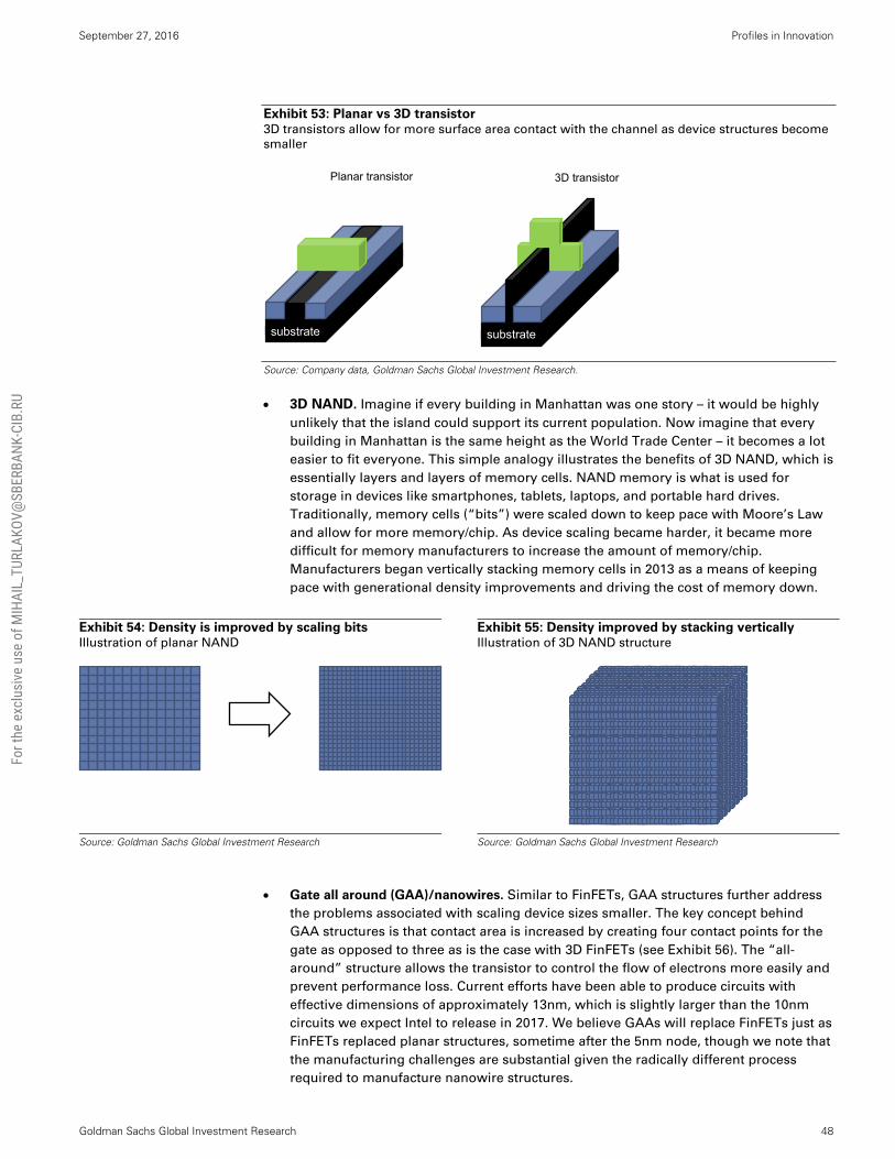
September 27, 2016 Profiles in Innovation
Goldman Sachs Global Investment Research 48
Exhibit 53: Planar vs 3D transistor 3D transistors allow for more surface area contact with the channel as device structures become
smaller
Source: Company data, Goldman Sachs Global Investment Research.
3D NAND. Imagine if every building in Manhattan was one story – it would be highly
unlikely that the island could support its current population. Now imagine that every
building in Manhattan is the same height as the World Trade Center – it becomes a lot
easier to fit everyone. This simple analogy illustrates the benefits of 3D NAND, which is
essentially layers and layers of memory cells. NAND memory is what is used for
storage in devices like smartphones, tablets, laptops, and portable hard drives.
Traditionally, memory cells (“bits”) were scaled down to keep pace with Moore’s Law
and allow for more memory/chip. As device scaling became harder, it became more
difficult for memory manufacturers to increase the amount of memory/chip.
Manufacturers began vertically stacking memory cells in 2013 as a means of keeping
pace with generational density improvements and driving the cost of memory down.
Exhibit 54: Density is improved by scaling bits Illustration of planar NAND
Exhibit 55: Density improved by stacking vertically Illustration of 3D NAND structure
Source: Goldman Sachs Global Investment Research
Source: Goldman Sachs Global Investment Research
Gate all around (GAA)/nanowires. Similar to FinFETs, GAA structures further address
the problems associated with scaling device sizes smaller. The key concept behind
GAA structures is that contact area is increased by creating four contact points for the
gate as opposed to three as is the case with 3D FinFETs (see Exhibit 56). The “all-
around” structure allows the transistor to control the flow of electrons more easily and
prevent performance loss. Current efforts have been able to produce circuits with
effective dimensions of approximately 13nm, which is slightly larger than the 10nm
circuits we expect Intel to release in 2017. We believe GAAs will replace FinFETs just as
FinFETs replaced planar structures, sometime after the 5nm node, though we note that
the manufacturing challenges are substantial given the radically different process
required to manufacture nanowire structures.
Planar transistor
substrate substrate
3D transistor
For t
he e
xclu
sive
use
of M
IHAI
L_TU
RLAK
OV@
SBER
BANK
-CIB
.RU

September 27, 2016 Profiles in Innovation
Goldman Sachs Global Investment Research 49
Exhibit 56: Gate all around (GAA) structure GAA structures allow for more surface area contact with the channel compared to 3D FinFET
Source: Goldman Sachs Global Investment Research
Commercialising the evolution of the semiconductor
In our previous discussions with Intel and as recently as the Intel Developer Forum (mid-
August 2016), management has demonstrated confidence in its ability to economically
scale to the 10nm and 7nm nodes, noting that 10nm cost/transistor is actually below the
historical trend. However, management has said EUV (extreme ultraviolet lithography) will
be needed to effectively produce 5nm chips. Intel is becoming increasingly confident that
in the next couple of years they will see an EUV tool that can provide stable power, which
should allow manufacturers to employ this technology.
That said, Mark Bohr, Intel’s director of process architecture and integration, has noted in
prior discussions with us that his team is working on other technologies to make 5nm
possible without EUV, including materials engineering. Mr. Bohr highlighted past
developments such as strained silicon, high-k metal gates, and FinFET as examples of the
types of projects the company is researching for implementation on future nodes, though
the company did not go into detail on its plans. Given that EUV has long been seen as a
game changer and is expected to finally be available at the 5nm node, we view Intel’s
continued focus on materials enabled innovations as illustrative of the importance of AMs
in the semiconductor market.
Key semi/SPE companies looking at alternate conductor materials:
Intel – Market share leader in consumer and data center microprocessors.
TSMC – Leading foundry used for manufacturing of applications processors and GPUs.
Samsung – One of the leading producers of memory chips and applications processors.
Applied Materials – Semiconductor production equipment company focused on
materials-enabled innovation.
source drainGate all around structure
For t
he e
xclu
sive
use
of M
IHAI
L_TU
RLAK
OV@
SBER
BANK
-CIB
.RU

September 27, 2016 Profiles in Innovation
Goldman Sachs Global Investment Research 50
For t
he e
xclu
sive
use
of M
IHAI
L_TU
RLAK
OV@
SBER
BANK
-CIB
.RU

September 27, 2016 Profiles in Innovation
Goldman Sachs Global Investment Research 51
Case studies
CASE STUDIES
1. Water filtration: Creating a sustainable future
2. Energy storage: The shift to renewables
3. Nanomedicine: A plethora of possibility
4. 5G communications: Speeding up the future
For t
he e
xclu
sive
use
of M
IHAI
L_TU
RLAK
OV@
SBER
BANK
-CIB
.RU

September 27, 2016 Profiles in Innovation
Goldman Sachs Global Investment Research 52
CASE STUDY 1 Water filtration: Creating a sustainable future
Population growth, climate change and urban creep are all placing increased pressure on
the world’s natural ecosystem. Water is becoming an increasingly scarce commodity. The
World Health Organisation (WHO) estimates that over 1 bn people do not have access to
clean water, and over 5,000 people die every day from deaths attributable to unsafe water,
sanitation and hygiene. The organization cites “better tools and procedures to improve and
protect drinking water quality” to improve water quality and maximize health benefits.
Exhibit 57: Sub-Saharan Africa has extremely scarce
sources of renewable water Total renewable water resources per capita (2013)
Exhibit 58: Almost US$8bn is spent on improving water
quality and sanitation in emerging markets US$bn spend on water and sanitation by NGOs and
governments in developing markets
Source: UNESCO
Source: OECD
To combat the challenge of ensuring sufficient potable water, governments and NGOs are
committing significant amounts of their R&D budgets to deliver a sustainable water
balance. NGOs are spending almost US$3bn pa directly on water and sanitation in
developing countries.
Bottling water is a means of transporting potable water, but the consumption and disposal
of plastics places other environmental strains on the environment. For instance, the
amount of energy required to meet US demand for plastic bottles is equivalent to 17mn
barrels of oil.
-40%
-20%
0%
20%
40%
60%
0
2
4
6
8
10
12
2000 2002 2004 2006 2008 2010 2012 2014
Tota
l Exp
endit
ure
(U
S$ b
n)
Government NGO's % yoy growth (RHS)
Advanced materials: Nanotechnology, graphene
Potential addressable markets:
US$8bn pa spent by governments on drinking water.
US$5bn pa spent on the global separation & membrane technology market with expectations for the market to double by 2020.
Bottled water market is around US$90bn with double-digit growth rates.
The opportunities:
Potential to prevent some of the 5,000 deaths per day from unsafe water, sanitation and hygiene.
Nanotechnology is being explored as a way of developing improved filtration/separation membranes.
Graphene is a possible material given its water-repelling properties.
For t
he e
xclu
sive
use
of M
IHAI
L_TU
RLAK
OV@
SBER
BANK
-CIB
.RU

September 27, 2016 Profiles in Innovation
Goldman Sachs Global Investment Research 53
Exhibit 59: Global bottled water market has almost
doubled in size in the past five years, placing increasing
pressure on the ecosystem. Bottled water consumption per capita
Exhibit 60: Chinese consumption of bottled water has
more than doubled in the past five, years indicating the
pressures from the development of emerging markets Bottled water consumption – total in gallons
Source: Bottledwater.org
Source: Bottledwater.org
The ability to provide a simple quality filtration process has the potential to both tackle the
emerging market water shortage and challenge the profit pools of the bottled water market.
Advanced Material filtration
Against this backdrop, graphene comes to the fore, particularly given its hydrophobic
properties. It has been discovered that thin membranes made from graphene oxide are
impermeable to all gases and vapors, besides water, and further research has shown it can
be made to allow separation of atomic materials that are very similar in size ‒ enabling
filtration at 9x the normal speed. This opens the door to the possibility of using seawater as
a drinking water resource, in a fast and relatively simple way. Furthermore, given
graphene’s small weight and size, the technology has the capability to be lightweight,
energy-efficient and environmentally friendly when making water filters and desalinators.
Companies: Nanofiltration the focus
Lockheed Martin has developed and patented a new energy efficient graphene-based water
desalination technology. The “Perforene” membrane is a one-atom thick sheet of graphene,
featuring holes all the way down to one nanometer in length. Integrating the membrane
within a filter of a larger system can trap unwanted substances and concurrently improve
the flow through of water molecules, reducing clogging and pressure on the membrane
and filter, lowering energy usage (by 10-20%) of the overall system.
Other firms working in nanofiltration include Dow, which is looking at a pressure-driven
separation process that employs a semi-permeable membrane and the principles of cross-
flow filtration. GE, Pentair, 3M, Koch and Siemens are also active in the field.
2009 2014
1 Mexico 59.2 69.8
2 Thailand 26.3 65.1
3 Italy 49.0 53.1
4 Belgium-Luxembourg 35.5 39.4
5 Germany 34.7 39.2
6 United Arab Emirates 25.0 41.6
7 France 34.4 37.4
8 United States 27.6 34.0
9 Spain 27.7 32.1
10 Hong Kong 22.2 32.7
11 Lebanon 30.1 28.2
12 Croatia 26.5 29.1
13 Slovenia 26.6 28.4
14 Hungary 27.9 28.8
15 Saudi Arabia 27.0 29.9
16 Switzerland 25.6 28.0
17 Austria 23.1 24.3
18 Brazil 22.0 25.5
19 Poland 19.7 25.0
20 Romania 19.8 23.2
7.8 10.3
Rank CountriesGallons per Capita
Global Average
2009 2014
1 China 5692 11459 15.0%
2 United States 8453 10875 5.2%
3 Mexico 892 8645 4.6%
4 Indonesia 2941 5307 12.5%
5 Brazil 4255 5151 3.9%
6 Thailand 1743 4376 20.2%
7 Italy 2949 3241 1.9%
8 Germany 2843 3227 2.6%
9 France 2165 2411 2.2%
10 India 1112 2069 13.2%
Top 10 Total 33044 56760 7.8%
All Others 14513 17948 4.3%
World Total 47558 74708 6.9%
Millions of GallonsRank Countries CAGR (%)
For t
he e
xclu
sive
use
of M
IHAI
L_TU
RLAK
OV@
SBER
BANK
-CIB
.RU

September 27, 2016 Profiles in Innovation
Goldman Sachs Global Investment Research 54
Energy storage: The shift to renewables
CASE STUDY 2
According to the International Energy Agency, global energy demand is expected to rise by
c.50% to 2030, with over 80% of current demand supplied by fossil fuels. In an increasingly
densely populated, but also environmentally conscious world, the ability to generate,
harness and utilise energy sources efficiently is vital to the sustainability and development
of the quality of life of the global citizen. Quite simply, renewable energy sources are the
way of the future.
Exhibit 61: Energy demand set to rise c.50% by 2040 Global energy demand
Exhibit 62: Energy storage part of the broader supply
chain complex Energy supply chains
Source: EIA
Source: EIA
Nanotech is set to play a vital role as an enabler and solution provider to one of the biggest
challenges we face. In the view of buckyball inventor, Nobel Prize winning Richard Smalley,
“Nanotechnology is the key to achieving a sustainable energy future.”
Nanotech is set to be influential in the early parts of the energy value chain, creating
efficiencies and better performance in a number of key areas. The International Energy
Commission estimates that 1 in every 2 research papers written about electrical storage
technology references nanotech.
500
550
600
650
700
750
800
850
2011 2012 2020 2025 2030 2035 2040
Quad
rill
ion
Btu
Sources Change Distribution Storage Usage
Advanced materials: Nanotechnology, graphene,
OLEDs
Potential addressable markets:
Supercapacitors: US$1bn
Nano-optimised photovoltaics: US$1bn
Catalysts: US$6bn
Nano-optimised fuel cells: US$5bn
The opportunities:
Nano-particles can alter and enhance the properties of bulk materials to deliver superior performance
Energy storage and conversion in solar cells can be greatly enhanced
Nano-electrodes can improve battery storage, discharge and re-charge rates
For t
he e
xclu
sive
use
of M
IHAI
L_TU
RLAK
OV@
SBER
BANK
-CIB
.RU

September 27, 2016 Profiles in Innovation
Goldman Sachs Global Investment Research 55
The use of nanotech in energy storage is a significantly rapidly growing area of nanotech
and AM, which has been driven by the green shift and mainstream utilisation of concepts
such as solar panels, EVs and off-grid battery storage.
In the area of energy storage, applications of nanotech mainly apply to improving
conversion rates, boosting recharge and dissipation rates, increasing efficiency and
lowering costs. The prime nano-areas being explored in the field include:
Nano electrodes: Perform similar to normal electrodes but on a nano scale. The high
surface to volume area of the nanoparticles lead to larger electrode contact areas and
thus enhance mass transport. The faster transport of the electrons results in enhanced
electrical and ionic conductivity – improving charge times is one example. Lithium-ion
batteries, supercapacitors, fuel cells and solar cells have all seen improved energy
performance due to nano-electrodes. Graphene/graphite are emerging materials but
other ‘traditional’ electrode/anode materials such as the metals (indium, zinc, etc.) are
also being broken down in to their nano-scale. Companies exposed include Sony,
Toshiba and Manz.
Nanocomposites: The inclusion of nanoparticles into a larger sample material. The
creation of nanocomposites results in enhanced physical properties of the macro
material. In energy storage, nanocomposites can be found in the electrolytic gel of
solar panels, the coating of the panels and in super capacitors. Nanoparticles are also
thought to be of use in devices converting carbon dioxide in to hydrocarbon fuels.
Companies exposed include BASF, 3M, and DuPont.
Nanocatalysts: The greater surface area of nanoparticles accelerates the catalytic
capacity of materials. Nanoscale platinum is used in hydrogen fuel cells and the use of
nanomaterials for catalytic convertors could improve environmental emissions.
The total addressable market for nanotech in energy storage is an exceptionally difficult
figure to define. As the end-product demand structurally accelerates (i.e., Tesla electric car
technology increases penetration rate) the need for AMs will intensify – both in terms of
growing physical demand, but also continued technological demand to continue to
improve the processes/technology that help deliver the cars their green credentials.
We estimate the current addressable market for nanotech in energy storage is around
US$10-15bn, and we believe this could grow to around US$20bn by 2020 (the base case
figure is based off International Electrotechnical Commission (IEC) research, and we have
utilised a 10% demand growth rate scenario). More aggressive demand growth of the end-
markets could see the TAM increased to an upper band of some US$30bn.
Visit our “Great Battery Race” portal for our latest thematic and company research on energy storage solutions.
For t
he e
xclu
sive
use
of M
IHAI
L_TU
RLAK
OV@
SBER
BANK
-CIB
.RU

September 27, 2016 Profiles in Innovation
Goldman Sachs Global Investment Research 56
Just as penicillin did in the 1940s, nanomedicine has the potential to revolutionize the way
we treat disease. The key advantage of nanomedicine is that it operates on the same scale
as many natural biological processes and molecules. If, utilizing the properties of
nanomedicine, medicines can be delivered and targeted directly to the impacted cells in the
specific dose required, the potential for a successful outcome may be increased. A targeted
drug approach should also reduce side effects and improve morbidity. Thus specific
tailored drugs and targeted delivery methods have the potential to increase the
personalization of disease treatment.
Along with disease treatment and management, nanotech has the potential to improve the
detection and prevention of disease. Through new contrast agents, nanomedicine can
improve on current diagnostic imaging capabilities, leading to earlier detection of disease
and ideally an improved prognosis.
The development of nanomedicine and nanobiology could significantly alter not only our
ability to prevent and treat disease, but also the profit pools of the existing pharmaceutical
and medical industries. Nanomedicine is already a rapidly growing industry with around
US$16bn of sales in 2015. R&D spend is growing with the NNI spending upward of
US$300m pa supporting R&D in to nanomedicine.
As an illustration, a 10% penetration of the existing US cancer treatment industry
represents a +US$10bn market for nanomedicine. These attractive profit pools, combined
with the medical benefits are what is attracting both small and large industry players such
as Intellia and Merrimack to lift their investment in and exposure to nanomedicine.
Advanced materials: Nanotechnology
Potential addressable markets:
The US oncology market is over US$100bn per annum. Assuming 10% penetration, the TAM for oncology nanomedicine in the US is potentially US$12bn plus per annum.
The opportunities:
Penicillin revolutionized the drug market in the 1940/50s. Nanotechnology could deliver the same scale of change in coming years.
Drug delivery can be targeted through nanotechnology to attack only sick cells, reducing side effects.
Diagnostics can be improved through nanotechnology allowing early detection and treatment.
Nanomedicine: A plethora of possibility
CASE STUDY 3
For t
he e
xclu
sive
use
of M
IHAI
L_TU
RLAK
OV@
SBER
BANK
-CIB
.RU

September 27, 2016 Profiles in Innovation
Goldman Sachs Global Investment Research 57
Exhibit 63: With viruses, antibodies and bacteria all operating on the nanoscale in our bodies, the utilisation of
nanotechnology in medical applications will allow for more specific targeting of diseases, leading to potentially better
recovery
Source: NCI, Goldman Sachs Global Investment Research.
The history and benefits of nanomedicines
One of the earliest nanomedicines, Doxil, was approved by the FDA in 1995. Since then
numerous other nanomedicines have been commercialized and approved with a broad
range of applications including treatment of cancer, fungal infections, and infection
prevention.
The physical properties of nanoparticles have a number of clinical benefits that are of
interest to clinicians and industry. Operating at the nanoscale could improve both the
efficacy of treatments and how drugs interact with the human body, i.e. toxicity and side
effects. The benefits of nanotech for the pharmaceutical industry are based on:
Improved solubility: Nanoparticles have higher solubility than their bulk counterparts,
potentially enabling drugs with poor solubility to be reinvestigated. In addition, higher
solubility reduces the need to use organic solvents, which are toxic.
Higher permeability: The size of nanoparticles may enable them to cross physiological
barriers such as the blood brain barrier, or enter tumors. This has important
implications for drug delivery in numerous disease areas such as oncology and
neurology.
Longer circulation: Nanoparticles can be engineered to increase the circulation time of
drugs.
Large surface area: This increases the reactiveness of nanoparticles. The greater
surface allows nanoparticles drugs to engage with the impacted cells, allowing greater
ability for the drugs to work.
For t
he e
xclu
sive
use
of M
IHAI
L_TU
RLAK
OV@
SBER
BANK
-CIB
.RU

September 27, 2016 Profiles in Innovation
Goldman Sachs Global Investment Research 58
Exhibit 64: Pharmaceutical nanotechnology
Source: European Medicines Agency
From a drug delivery perspective, using nanomaterials to deliver drugs has several benefits
compared to existing delivery methods such as injections, pills etc.
Polymer-based materials can allow for better pharmacokinetics and bio distribution
of drugs
Triggered response techniques would allow drugs imbedded in the body to be
released when certain triggers are induced, allowing rapid and targeted drug delivery.
Key areas of focus
Nanomedicine has a vast array of potential applications, with two major interrelated areas
of focus, including drug delivery and disease diagnosis and monitoring.
Drug delivery: Nanopharmaceuticals can either be reduced to the nanoscale or
engineered at the nanoscale, and functionalized to have specific characteristics. These
characteristics can enable targeted drug delivery directly to the area of focus along
with customized drug release, improving treatment efficacy and reducing side effects
for the patient.
Medical diagnostics: Earlier detection of disease would aid the ability of physicians
to treat these diseases, for instance detecting cancer pre metastasis, potentially
improving treatment success rates.
For t
he e
xclu
sive
use
of M
IHAI
L_TU
RLAK
OV@
SBER
BANK
-CIB
.RU

September 27, 2016 Profiles in Innovation
Goldman Sachs Global Investment Research 59
Drug delivery
Through physical and chemical modifications, nanomedicines can be “functionalized” to
have certain characteristics, enabling different clinical applications. In particular,
nanoparticles can be engineered to target particular areas of the body through the use of
biomarkers and molecules such as peptides and nucleic acids. These nanoparticles can be
further modified so that, once delivered, they release their drug load in a controlled
manner. Triggers for drug delivery may include pH, light, or tumor specific conditions. Key
benefits of this targeted drug delivery include reduced dose size and lower side effects (it is
important to note that the nanoscale of these drugs can also result in disparate side effects/
toxicities to their bulk counterparts).
This technology has been and has the potential to be applied in numerous clinical areas
including cancer and neurodegenerative disorders. The majority of clinically available
nanomedicines in this are either liposomes or polymer-based nanoformulations.
Treatment of solid tumors
Numerous different treatment methods have been developed and are in development for
cancers using nanomedicine. In treating solid tumors, nanoparticles are able to utilize the
enhanced permeability and retention (ERP) effect whereby the reduced lymphatic drainage
of tumors result in nanoparticles being accumulated and retained. This ERP effect is also
referred to as passive targeting.
Neurological diseases
Treatment of diseases of the central nervous system (CNS) are challenged by the existence
of barriers, including the blood brain barrier (BBB) and blood cerebrospinal fluid barrier
(BCSF), which selectively prevent molecules from crossing from the bloodstream into the
CNS. Molecules blocked from entering the brain, for instance, include most traditional
pharmaceuticals and chemotherapy.
An exciting horizon for nanomedicine is therefore the development of nanomolecules that
are able to cross the BBB/BCSF given their small size and molecular weight. Conditions that
could be targeted include neuro-oncology, Alzheimer’s/dementia, stroke and epilepsy.
Medical diagnostics
In addition to the treatment of disease, nanomedicine shows promise in detection and
monitoring.
Medical imaging
According to the National Cancer Institute, traditional diagnostic imaging (DI) techniques in
use today are only able to detect cancers once tissue has altered visibly. This means that
diagnosis could occur post metastasis (spread to secondary organ/ tissue), greatly reducing
the likelihood that treatment will be successful. In addition, to gain further information on
tumors (e.g. malignant or benign), an invasive biopsy must often be taken.
Nanotech has the potential to improve upon this status quo, principally through new
contrast agents. Nanoparticles such as superparamagnetic iron oxide nanoparticles can be
engineered to target and accumulate at the tumor site. In addition, contrast agents could be
developed that identify characteristics of the tumor such as type and the stage the cancer is
at.
Biomarkers
The National Cancer Institute defines biomarkers (biological marker) as “a biological
molecule found in blood, other body fluids, or tissues that is a sign of a normal or
abnormal process, or of a condition or disease. A biomarker may be used to see how well
the body responds to a treatment for a disease or condition”. Nanomedicine offers the
potential to detect changes that have occurred in only a small number of cells.
For t
he e
xclu
sive
use
of M
IHAI
L_TU
RLAK
OV@
SBER
BANK
-CIB
.RU

September 27, 2016 Profiles in Innovation
Goldman Sachs Global Investment Research 60
Quantum dots (QD) are a type of nanomedicine commonly cited for this purpose, given
that these nanocrystals are fluorescent, display different colors depending on size, and are
far brighter in vivo than organic dyes. In addition, QDs are able to circulate throughout the
body due to their small size, enabling tumors to be targeted. However, as is the case with a
number of potential nanomedicines, whilst QDs show tremendous potential, there are
toxicity concerns that must be addressed before human application
Multipurpose nanomedicines - theranostic
An ideal outcome from the development of nanomedicine would be the commercialization
of nanoparticles that have both therapeutic and diagnostic uses (theranostic - therapy
diagnostic). For example, a drug that is able to target and release its load at a particular
tumor site, while also enabling DI to track the progress and success of this treatment.
In addition to the applications discussed above, there are a multitude of existing and
potential clinical applications of nanomedicine. Key areas of interest include non-viral gene
vector delivery, regenerative medicine/ tissue engineering and implantable nanodevices.
The opportunity: Looking forward/profit pools
The opportunities for nanotech to alter the medicinal and pharmaceutical field are
significant and wide ranging. To provide some context to the scale of opportunity and
potential profit pools, we look at two areas where we see nanotech having a significant
impact: i) oncology, which has existing commercialized nanomedicines, and ii) gene
therapy, which is in the investigational phase.
New frontiers in cancer treatment and market opportunity (>US$10bn market)
According to the Centres for Disease Control and Prevention (CDC), cancer was the cause
of just under 600,000 deaths in the US in 2014, the second-highest cause after
cardiovascular disease. The National Cancer Institute (NCI) expects that in the US there will
be 1,690,000 new cases diagnosed with c. 600,000 deaths in 2016 alone.
Current treatments include chemotherapy, immunotherapy, surgery and radiation therapy.
These have downsides including their non-targeted nature; for example, chemotherapy
impacts healthy tissue as well the tumor of interest, resulting in common side effects such
as hair loss.
Nanomedicines for the treatment of cancer have been commercially available for a number
of years; indeed, Doxil was first approved by the FDA in 1995 for the treatment of AIDS-
related Kaposi’s sarcoma and has now gone generic. The majority of these approved
treatments, however, are non-targeted. Therefore, they are commonly considered first-
generation nanomedicines. For example, first generation breast cancer treatment Abraxane
targets tumors passively through the ERP effect.
Second generation cancer treatments would actively target tumor tissue, effectively a form
of personalized medicine. There are currently no second generation nanoparticles clinically
available; however, there are a number of actively targeted treatments in phase I or II
clinical trials.
Treatment costs in the US amounted to just under US$125bn in 2010, and the NCI projects
total expenditure of US$156bn in 2020. If we assume a 10% penetration of nano-oncology,
the potential is for a c.US$12bn plus market per annum.
Nanomedicine in genetic disorders
Gene therapy, and its closely related field genome editing, are being investigated for a
wide range of genetic disorders, with a small number of therapies approved in different
For t
he e
xclu
sive
use
of M
IHAI
L_TU
RLAK
OV@
SBER
BANK
-CIB
.RU

September 27, 2016 Profiles in Innovation
Goldman Sachs Global Investment Research 61
jurisdictions. Broadly, gene therapies involve inserting into a cell a copy of the desired
gene, whereas genome editing ‘edits’ genomes inside the cell.
In developing a gene therapy, a key area of consideration is the delivery method chosen. A
large number of programs utilise viral vectors, e.g. adeno-associated viral vectors (AAV),
such as Spark Therapeutic’s SPK-FIX for hemophilia B, however, viral vectors face safety
concerns. Nanotechnologies provide potential alternatives to viral vectors, i.e. non-viral or
synthetic vectors, and are being explored by a number of biotech companies:
Intellia Therapeutics (NTLX): Intellia is investigating the use of genome editing
technology CRISPR/ Cas9 for a range of conditions including alpha 1 antitrypsin
deficiency, transthyretin amyloidosis and hepatitis B. As these diseases relate to the
liver, Intellia is utilizing lipid nanoparticles to deliver the technology to the liver.
Editas Medicine (EDIT): Similarly to Intellia, Editas identifies lipid nanoparticles as a
means of targeting CRISPR to the disease area. Editas is investigating diseases ranging
from Duchenne Muscular Dystrophy, alpha 1 antitrypsin deficiency and cystic fibrosis.
To illustrate the genetic conditions being investigated by these companies, we look at
alpha 1 antitrypsin deficiency. Current treatment includes replacement therapy, where
patients are infused with plasma derived alpha 1 antitrypsin. CSL and Grifols are the two
largest producers of alpha 1 antitrypsin; the Marketing Research Bureau estimates that
total US sales of alpha 1 antitrypsin were US$690mn in 2015.
For t
he e
xclu
sive
use
of M
IHAI
L_TU
RLAK
OV@
SBER
BANK
-CIB
.RU

September 27, 2016 Profiles in Innovation
Goldman Sachs Global Investment Research 62
We see GaN as a potential disrupter of the LDMOS power amplifier market
Gallium nitride (GaN) is a III-V compound used most often in radio frequency (RF) devices
for mobile communications as well as communications infrastructure applications. Key
suppliers include MACOM (MTSI, covered by Mark Delaney) and Qorvo (QRVO, covered by
Toshiya Hari). Given that they are III-V compounds and thus have higher bandgaps, GaN
devices offer significantly better performance over other compound and silicon-based
technologies today. Due to the higher bandgap, GaN chips are able to perform better than
silicon devices at higher frequencies, voltages, power densities and temperatures, making
them particularly applicable to 5G networks, which are expected to utilize spectrum at
higher frequencies than today’s networks. On the network infrastructure side, we see GaN
as a potential disrupter of the ~US$1bn LDMOS power amplifier market.
Exhibit 65: GaN offers greater performance compared to GaAs and silicon chips in power
and RF applications GaN vs. GaAs and Si on key metrics
Source: GaN Systems, Goldman Sachs Global Investment Research.
5G communications: Speeding up the future
CASE STUDY 4
Advanced materials: Gallium nitride (GaN)
Potential addressable markets:
Communications infrastructure: US$1bn
Defense applications: US$1bn
The opportunities:
Enabling use of higher frequency spectrum
Driving faster data speeds and greater bandwidth
Providing greater energy efficiency
For t
he e
xclu
sive
use
of M
IHAI
L_TU
RLAK
OV@
SBER
BANK
-CIB
.RU

September 27, 2016 Profiles in Innovation
Goldman Sachs Global Investment Research 63
Today RF devices primarily utilize compound technologies such as gallium arsenide (GaAs)
and silicon-based technologies such as silicon germanium (SiGe). GaN currently occupies
niche segments including radar and comms/cable infrastructure, with many of these
applications are subsidized by government funding (see Exhibit 66). Out of a total high
performance RF market of ~US$3bn, GaN revenue accounted for US$300mn in 2015 and is
expected to grow to almost US$1bn by 2022.
Exhibit 66: The GaN market was about US$300mn in 2015 and is expected to grow to
almost US$1bn by 2022 GaN market by application
Source: Yole Development
While GaN technology has been in development for several years, chip companies have
only recently begun applying GaN in more applications. Applications for GaN include RF
applications for frequencies of 10GHz+, power semiconductors, and DC switching, where
GaN technology is able to withstand significantly higher voltages.
Key drivers of future growth for GaN include 5G base station deployment and defense
spending. For example, Qorvo estimates that these areas could enable the GaN market to
potentially grow at a 25% CAGR. One of the biggest trends that we are monitoring though
is the coming 5G network infrastructure build out. 5G will extend the range of frequencies
used for cellular communication in order to be able to handle increased traffic capacity and
enable bandwidths required for very high data rates. In the past, high-frequency spectrum
has not played a major role in wireless networks because the shorter wavelengths do not
travel over long distances. While 5G technology does not fundamentally overcome this
challenge, we expect 5G to be deployed as carriers densify their networks and believe
higher frequency spectrum will become increasingly useful because signals will not need
to travel as far from cell sites to reach customers.
Communications networks are made up of base stations that transmit and receive radio
signals. Currently, the power amplifier portion of the base station market is dominated by
LDMOS power amplifiers, though we highlight the potential for GaN to disrupt this
dynamic given that 5G networks are expected to utilize higher spectrum frequencies, i.e. up
to 100GHz, which are better serviced by GaN technology.
Wireless infrastructure,
55%
Defense, 37%
CATV, 4%Other, 4%
Satellite communications,
1%
For more on the coming 5G revolution, including companies that could benefit, see Simona Jankowski’s April 2016 deep dive.
For t
he e
xclu
sive
use
of M
IHAI
L_TU
RLAK
OV@
SBER
BANK
-CIB
.RU

September 27, 2016 Profiles in Innovation
Goldman Sachs Global Investment Research 64
Companies
MACOM (MTSI, covered by Mark Delaney) MACOM is an analog and photonic
semiconductor company with about 70% of its revenue derived from the communications
end-market. MACOM’s revenue has historically been tied to applications in long-haul
optical, CATV, and PON. However, the company is targeting new growth opportunities in
base stations, metro, and datacenters. MACOM offers GaN on silicon power amplifier chips
and hopes to be able to gain share in the roughly US$1 bn annual base station PA end-
market. We believe that while MACOM has the potential to penetrate this market in late
2016 or 2017 with its GaN on silicon technology for LTE (as MACOM’s approach to GaN can
be done at competitive costs), and that the higher frequencies used in 5G will require the
performance of GaN semiconductors that companies such as MACOM offer. In addition,
MACOM believes its GaN technology will allow it to improve performance in other
applications such as microwaves and its catalog portfolio.
Qorvo (QRVO, covered by Toshiya Hari). Qorvo is an RF communication company with
about 20% of revenue derived from the comms infrastructure and defense markets (the
remainder is primarily from handset RF solutions). Like MACOM, the company offers GaN
process expertise and has highlighted both 5G and military applications (i.e. radar and
electronic warfare applications) as key driver of growth for its infrastructure product
portfolio. Management has noted that new defense applications represent a potential
US$500mn+ market for GaN products.
For t
he e
xclu
sive
use
of M
IHAI
L_TU
RLAK
OV@
SBER
BANK
-CIB
.RU

September 27, 2016 Profiles in Innovation
Goldman Sachs Global Investment Research 65
An interview with Dr. John Chen, Phoenix Venture Partners
Dr. John Chen, Phoenix Venture Partners
Dr. Chen is a Managing
General Partner and co-
founder of Phoenix Venture
Partners (PVP). Phoenix
Venture Partners is a
specialist fund that looks for
transformative advanced
materials innovations,
including novel engineered
materials, new device architectures, and advanced process
technologies and tools. PVP invests in innovations that
enable entirely new products, dramatic performance
improvements of existing products, enhanced-efficiency,
and/or greener manufacturing processes for major industries
such as Consumer Electronics, Drug
Delivery, Chemicals, Energy Generation, Energy
Storage, Solar, Water, and Building Materials, to name a
few.
Dr. Chen earned his BS in Physics, PhD in Materials Science
and Engineering, and MBA from MIT. In addition to
his investment and board roles with PVP, Dr. Chen serves on
the Commercialization Advisory Board for Oregon Built
Environment & Sustainability Technologies (BEST), is an
active mentor to several startups through the MIT Venture
Mentoring Service, and is a long-time member of the
Materials Research Society
Advanced materials is an extremely wide ranging and
broad topic, so let’s start off by asking how you would
define an advanced material.
You are absolutely correct to observe that advanced
materials encompasses an extremely diverse and broad set
of technologies. At PVP, we have loosely defined advanced
materials as a collection of technologies that include novel
engineered materials, device architectures, processes, and
metrology/tools which enable disruptive performance
through the precision engineering, design, and or
measurement of molecular scale properties. Advanced
materials or materials science based technologies are also
interdisciplinary in nature drawing
from physics, chemistry, biology, and the engineering
disciplines.
What, in your view, makes the advanced materials
space so attractive from a VC perspective?
PVP sees the advanced materials space as highly attractive
from an investment perspective because these
technologies have the potential to generate significant
value by enabling next-generation product performance as
well as delivering disruptive cost reduction and
manufacturing efficiencies for both well-established and
rapidly emerging markets. The platform nature of
advanced materials technologies also often allows them to
enable applications that transcend industry verticals which
can lead to multiple exit scenarios. The advanced materials
space is experiencing a sustained wave of rapid innovation
which has been fueled by decades of R&D investment by
both the private and public sectors. From a VC perspective,
the advanced materials space is also attractive because
startups don’t face the extreme competitive pressures of
other sectors (e.g., software, consumer internet) and very
few venture capital firms are active in this area and even
fewer have the necessary teams, expertise or track record
to be successful in this space.
In terms of your investment process, would you
describe it as top-down (sector preferences then drill
down into the most appropriate company to reflect the
theme) or bottom up (very company fundamental
specific)?
By the very nature of the advanced materials space, PVP
employs a unique investment process which is a bit of
both. Without going into too much detail, PVP proactively
researches and looks at the unmet needs of critically
important industry sectors (e.g. energy storage, consumer
electronics, life sciences, etc.) and keeps track of disruptive
emerging technology trends (e.g. printed electronics, 3D
printing, graphene, etc.) to formulate our investment thesis
while also maintaining an extensive network and robust
global scouting platform to find the most promising
startups developing breakthrough technologies.
For t
he e
xclu
sive
use
of M
IHAI
L_TU
RLAK
OV@
SBER
BANK
-CIB
.RU

September 27, 2016 Profiles in Innovation
Goldman Sachs Global Investment Research 66
As a VC, what makes investing in the advanced materials
space different from other sectors? What are the unique
skills you need to succeed here versus elsewhere? What
are the main challenges you face operating in the
advanced materials space?
Several characteristics of the advanced materials space
make it a challenging sector to invest in for generalist VCs.
The enormous scope, diversity and technical complexity of
advanced materials technologies requires an investment
team which has deep domain knowledge in specific fields of
science and engineering (i.e. PhD level) as well as
multidisciplinary and complimentary backgrounds (e.g.
materials science, physics, chemistry, life sciences, etc.) to
be able to adequately evaluate investment opportunities and
recognize truly disruptive companies from me-too’s.
Compared to other sectors, a greater degree of detailed
knowledge of IP and IP strategy is key to creating and
preserving long-term value. It is also critically important that
investors in this space have had first-hand experience of the
challenges and hurdles startups face building a successful
company and getting advanced materials technologies
adopted by the market so that they can navigate portfolio
companies through the inevitable difficult times. Last but not
least, experienced investors in the advanced materials space
know from the “school of hard knocks” which business
models to pursue and which to avoid.
Is there one or two sectors within the advanced
materials space, e.g. Solar, Building materials, consumer
electronics etc. that you believe stands out in terms of
growth?
Many sectors within advanced materials are growing rapidly
but off hand two that come to mind are energy storage
materials and graphene.
Can you give us a brief guide into a typical investment
lifecycle? How long is the process between idea
generation and actual investment in a company? What
are the main sticking points/obstacles you face in that
lifecycle?
Every investment is unique and follows its own timeline and
venture capital is more of an art than a science. Some of our
investments take 3 months from start to end and others we
have tracked for three years until they satisfied our criteria
for investment and we closed the investment.
Advanced materials is an evolving yet under invested area of innovation. Why do you think that is? Is it because of the technical skillset and expertise required, or lack of awareness of how rapidly the industry is growing?
Advanced materials is an under-served sector for venture
capitalists for many reasons. The formidable barriers to
entry and being successful I alluded to in the previous
question dissuade many investors from taking the plunge.
Second, for the uninitiated an untrained, much of the
innovation falls under the radar screen of mainstream
media and is also often miscategorized and lumped into
other “hotter” sectors such as clean tech, energy, life
sciences and IT. Finally, for reasons I don’t entirely
understand, investors have a mistaken perception that
advanced materials is a “niche” market and not very
attractive. I’d like to point out to your readers that the
entire semiconductor industry is based on advanced
materials innovations (e.g. silicon processing, copper
deposition, photolithography, etc.), the revolution in
electric vehicles is being driven largely by advances in new
materials for Li-ion batteries (e.g., cathodes, anodes,
separators, electrolytes, etc.), and the widespread adoption
of cheap solar energy was in part enabled by new
materials (e.g. CdTe, CIGS), just to name a few examples.
How large and industry do you think the broad
categories of advanced materials can become?
PVP investment professionals have been directly involved
in the advanced materials space for decades and these
estimates are provided by our own proprietary research as
well as from publicly available market research on sectors
which overlap with and are decent proxies for advanced
materials such as nanotechnology, clean tech,
printed/organic electronics, additive manufacturing, etc.
That said, systematic and accurate coverage of this space
and its impact on industry is far from perfect. If I were to
make a best guess I would say US$3trn is the industrial
impact of advanced materials innovation over the next ten
years, which is likely to be conservative and
underestimates the true impact.
For t
he e
xclu
sive
use
of M
IHAI
L_TU
RLAK
OV@
SBER
BANK
-CIB
.RU

September 27, 2016 Profiles in Innovation
Goldman Sachs Global Investment Research 67
Disclosure Appendix
Reg AC
We, Craig Sainsbury, Jay Shyam, CFA, Shuhei Nakamura, Toshiya Hari, Marcus Shin, Charles Long, Robert D. Boroujerdi, Hugo Scott-Gall, Ian
Abbott, Shin Horie, Richard Manley, Brian Lee, CFA, Matthew McNee, Grace Fulton, Giuni Lee, Ken Lek, Ayaka Misonou, Frank He, Julian Zhu, Eddie
Ow, CFA, Anita Dinshaw and Isabelle Dawson, hereby certify that all of the views expressed in this report accurately reflect our personal views about
the subject company or companies and its or their securities. We also certify that no part of our compensation was, is or will be, directly or indirectly,
related to the specific recommendations or views expressed in this report.
I, Peter Callahan, hereby certify that all of the views expressed in this report accurately reflect my personal views, which have not been influenced by
considerations of the firm's business or client relationships.
Unless otherwise stated, the individuals listed on the cover page of this report are analysts in Goldman Sachs' Global Investment Research division.
Investment Profile
The Goldman Sachs Investment Profile provides investment context for a security by comparing key attributes of that security to its peer group and
market. The four key attributes depicted are: growth, returns, multiple and volatility. Growth, returns and multiple are indexed based on composites
of several methodologies to determine the stocks percentile ranking within the region's coverage universe.
The precise calculation of each metric may vary depending on the fiscal year, industry and region but the standard approach is as follows:
Growth is a composite of next year's estimate over current year's estimate, e.g. EPS, EBITDA, Revenue. Return is a year one prospective aggregate
of various return on capital measures, e.g. CROCI, ROACE, and ROE. Multiple is a composite of one-year forward valuation ratios, e.g. P/E, dividend
yield, EV/FCF, EV/EBITDA, EV/DACF, Price/Book. Volatility is measured as trailing twelve-month volatility adjusted for dividends.
Quantum
Quantum is Goldman Sachs' proprietary database providing access to detailed financial statement histories, forecasts and ratios. It can be used for
in-depth analysis of a single company, or to make comparisons between companies in different sectors and markets.
GS SUSTAIN
GS SUSTAIN is a global investment strategy aimed at long-term, long-only performance with a low turnover of ideas. The GS SUSTAIN focus list
includes leaders our analysis shows to be well positioned to deliver long term outperformance through sustained competitive advantage and
superior returns on capital relative to their global industry peers. Leaders are identified based on quantifiable analysis of three aspects of corporate
performance: cash return on cash invested, industry positioning and management quality (the effectiveness of companies' management of the
environmental, social and governance issues facing their industry).
Disclosures
Coverage group(s) of stocks by primary analyst(s)
Craig Sainsbury: Australia-Resources. Shuhei Nakamura: Japan-Advanced Materials sector. Toshiya Hari: America-Semiconductor Capital Equipment,
America-Semiconductors. Marcus Shin: Korea Technology. Ian Abbott: Australia-Healthcare. Brian Lee, CFA: America-Clean Energy, America-Solar
Energy. Matthew McNee: Australia-Agriculture, Australia-Building Materials, Australia-Chemicals. Frank He: Asia Pacific Conglomerates, China Clean
Energy. Julian Zhu: Asia Commodities Companies.
America-Clean Energy: Acuity Brands Inc., Cree Inc., Silver Spring Networks Inc., TerraVia Holdings, Universal Display Corp., Veeco Instruments Inc..
America-Semiconductor Capital Equipment: Applied Materials Inc., Keysight Technologies Inc., Lam Research Corp., SunEdison Semiconductor Ltd.,
Teradyne Inc..
America-Semiconductors: Analog Devices Inc., Broadcom Ltd., Intel Corp., Linear Technology Corp., Maxim Integrated Products, Nvidia Corp., NXP
Semiconductors NV, Qorvo Inc., Skyworks Solutions Inc., Texas Instruments Inc., Xilinx Corp..
America-Solar Energy: 8point3 Energy Partners, First Solar Inc., SolarCity Corp., SolarEdge Technologies Inc., SunPower Corp., Sunrun Inc.,
TerraForm Global Inc., TerraForm Power Inc., Vivint Solar Inc..
Asia Commodities Companies: ACC Ltd., Aluminum Corp. of China (A), Aluminum Corp. of China (H), Ambuja Cements, Angang Steel (A), Angang
Steel (H), Anhui Conch Cement (A), Anhui Conch Cement (H), Baoshan Iron & Steel, BBMG Corp. (A), BBMG Corp. (H), Beijing Enterprises Water
Group, Beijing Originwater Technology, Beijing Water Business Doctor, China Coal Energy (A), China Coal Energy (H), China Conch Venture Holdings,
China Everbright International Ltd., China Hongqiao Group, China Molybdenum Co., China National Building Material, China Resources Cement
Holdings, China Shenhua Energy (A), China Shenhua Energy (H), Dongjiang Environmental Co. (A), Dongjiang Environmental Co. (H), GrandBlue
Environment Co., Jiangxi Copper (A), Jiangxi Copper (H), Maanshan Iron & Steel (A), Maanshan Iron & Steel (H), Shree Cement Ltd., Tianjin Capital
Environmental (A), Tianjin Capital Environmental (H), Tianjin Motimo Membrane Tech, TUS-Sound, Ultratech Cement, Yanzhou Coal Mining (A),
Yanzhou Coal Mining (H), Zhaojin Mining Industry, Zijin Mining (A), Zijin Mining (H).
Asia Pacific Conglomerates: Beijing Enterprises Holdings, Cheung Kong Infrastructure, China Gas Holdings, China Merchants Holdings, China
Resources Gas Group, China Suntien Green Energy, CITIC Ltd., CK Hutchison Holdings, COSCO Pacific, ENN Energy Holdings, Fosun International,
Galaxy Entertainment Group, Hutchison Port Holdings, Jardine Matheson, Kunlun Energy Co., Legend Holdings, Melco Crown Entertainment (ADR),
Melco International Development, MGM China, MTR Corp., Sands China, Shanghai Industrial, Sinopec Kantons, SJM Holdings, Summit Ascent
Holdings, Swire Pacific, Tianhe Chemicals Group, Towngas China, Wharf Holdings, Wheelock and Co., Wynn Macau.
Australia-Agriculture: Costa Group, GrainCorp Ltd., Nufarm.
Australia-Building Materials: Adelaide Brighton, Boral, CSR, James Hardie.
Australia-Chemicals: Incitec Pivot Ltd., Orica Ltd..
Australia-Healthcare: Ansell, Australian Pharmaceutical Inds., Cochlear Ltd., CSL Ltd., EBOS Group, Fisher & Paykel Healthcare, Healthscope Ltd.,
Medibank Private Ltd., NIB Holdings, Primary Health Care, Ramsay Health Care, ResMed Inc., Sigma Pharmaceuticals, Sonic Healthcare.
For t
he e
xclu
sive
use
of M
IHAI
L_TU
RLAK
OV@
SBER
BANK
-CIB
.RU

September 27, 2016 Profiles in Innovation
Goldman Sachs Global Investment Research 68
Australia-Resources: Alumina, BHP Billiton, Fortescue Metals Group, Iluka Resources, Independence Group, Newcrest Mining, Northern Star
Resources Ltd., OZ Minerals, Regis Resources, Rio Tinto, Sandfire Resources, South32 Ltd., Western Areas.
China Clean Energy: Canadian Solar Inc., China High Speed Transmission, GCL-Poly Energy Holdings, JinkoSolar Holding, Longi Silicon Materials,
Shenzhen Clou Electronics Co., Singyes Solar, Sungrow Power Supply Co., Trina Solar, Xinjiang Goldwind (A), Xinjiang Goldwind (H), Xinyi Solar
Holdings.
Japan-Advanced Materials sector: Daicel, Daido Steel, Hitachi Metals, JFE Holdings, Kansai Paint, Kobe Steel, Kuraray, Nippon Carbon, Nippon Paint
Holdings, Nippon Shokubai, Nippon Steel & Sumitomo Metal, Tokyo Steel Manufacturing, Toray Industries, UACJ.
Korea Technology: Samsung Electro-Mechanics, Samsung Electronics, Samsung SDI Co., Samsung SDS Co., Seoul Semiconductor, SK Hynix Inc..
Company-specific regulatory disclosures
Compendium report: please see disclosures at http://www.gs.com/research/hedge.html. Disclosures applicable to the companies included in this
compendium can be found in the latest relevant published research
Distribution of ratings/investment banking relationships
Goldman Sachs Investment Research global Equity coverage universe
Rating Distribution Investment Banking Relationships
Buy Hold Sell Buy Hold Sell
Global 31% 54% 15% 66% 60% 50%
As of July 1, 2016, Goldman Sachs Global Investment Research had investment ratings on 2,963 equity securities. Goldman Sachs assigns stocks as
Buys and Sells on various regional Investment Lists; stocks not so assigned are deemed Neutral. Such assignments equate to Buy, Hold and Sell for
the purposes of the above disclosure required by the FINRA Rules. See 'Ratings, Coverage groups and views and related definitions' below. The
Investment Banking Relationships chart reflects the percentage of subject companies within each rating category for whom Goldman Sachs has
provided investment banking services within the previous twelve months.
Price target and rating history chart(s)
Compendium report: please see disclosures at http://www.gs.com/research/hedge.html. Disclosures applicable to the companies included in this
compendium can be found in the latest relevant published research
Regulatory disclosures
Disclosures required by United States laws and regulations
See company-specific regulatory disclosures above for any of the following disclosures required as to companies referred to in this report: manager
or co-manager in a pending transaction; 1% or other ownership; compensation for certain services; types of client relationships; managed/co-
managed public offerings in prior periods; directorships; for equity securities, market making and/or specialist role. Goldman Sachs trades or may
trade as a principal in debt securities (or in related derivatives) of issuers discussed in this report.
The following are additional required disclosures: Ownership and material conflicts of interest: Goldman Sachs policy prohibits its analysts,
professionals reporting to analysts and members of their households from owning securities of any company in the analyst's area of
coverage. Analyst compensation: Analysts are paid in part based on the profitability of Goldman Sachs, which includes investment banking
revenues. Analyst as officer or director: Goldman Sachs policy prohibits its analysts, persons reporting to analysts or members of their
households from serving as an officer, director, advisory board member or employee of any company in the analyst's area of coverage. Non-U.S. Analysts: Non-U.S. analysts may not be associated persons of Goldman, Sachs & Co. and therefore may not be subject to FINRA Rule 2241 or FINRA
Rule 2242 restrictions on communications with subject company, public appearances and trading securities held by the analysts.
Distribution of ratings: See the distribution of ratings disclosure above. Price chart: See the price chart, with changes of ratings and price targets in
prior periods, above, or, if electronic format or if with respect to multiple companies which are the subject of this report, on the Goldman Sachs
website at http://www.gs.com/research/hedge.html.
Additional disclosures required under the laws and regulations of jurisdictions other than the United States
The following disclosures are those required by the jurisdiction indicated, except to the extent already made above pursuant to United States laws
and regulations. Australia: Goldman Sachs Australia Pty Ltd and its affiliates are not authorised deposit-taking institutions (as that term is defined in
the Banking Act 1959 (Cth)) in Australia and do not provide banking services, nor carry on a banking business, in Australia. This research, and any
access to it, is intended only for "wholesale clients" within the meaning of the Australian Corporations Act, unless otherwise agreed by Goldman
Sachs. In producing research reports, members of the Global Investment Research Division of Goldman Sachs Australia may attend site visits and
other meetings hosted by the issuers the subject of its research reports. In some instances the costs of such site visits or meetings may be met in part
or in whole by the issuers concerned if Goldman Sachs Australia considers it is appropriate and reasonable in the specific circumstances relating to
the site visit or meeting. Brazil: Disclosure information in relation to CVM Instruction 483 is available at
http://www.gs.com/worldwide/brazil/area/gir/index.html. Where applicable, the Brazil-registered analyst primarily responsible for the content of this
research report, as defined in Article 16 of CVM Instruction 483, is the first author named at the beginning of this report, unless indicated otherwise at
the end of the text. Canada: Goldman Sachs Canada Inc. is an affiliate of The Goldman Sachs Group Inc. and therefore is included in the company
specific disclosures relating to Goldman Sachs (as defined above). Goldman Sachs Canada Inc. has approved of, and agreed to take responsibility for,
this research report in Canada if and to the extent that Goldman Sachs Canada Inc. disseminates this research report to its clients. Hong Kong: Further information on the securities of covered companies referred to in this research may be obtained on request from Goldman Sachs
(Asia) L.L.C. India: Further information on the subject company or companies referred to in this research may be obtained from Goldman Sachs
(India) Securities Private Limited, Research Analyst - SEBI Registration Number INH000001493, 951-A, Rational House, Appasaheb Marathe Marg,
Prabhadevi, Mumbai 400 025, India, Corporate Identity Number U74140MH2006FTC160634, Phone +91 22 6616 9000, Fax +91 22 6616 9001. Goldman
Sachs may beneficially own 1% or more of the securities (as such term is defined in clause 2 (h) the Indian Securities Contracts (Regulation) Act,
1956) of the subject company or companies referred to in this research report. Japan: See below. Korea: Further information on the subject
company or companies referred to in this research may be obtained from Goldman Sachs (Asia) L.L.C., Seoul Branch. New Zealand: Goldman
Sachs New Zealand Limited and its affiliates are neither "registered banks" nor "deposit takers" (as defined in the Reserve Bank of New Zealand Act
1989) in New Zealand. This research, and any access to it, is intended for "wholesale clients" (as defined in the Financial Advisers Act 2008) unless
otherwise agreed by Goldman Sachs. Russia: Research reports distributed in the Russian Federation are not advertising as defined in the Russian
For t
he e
xclu
sive
use
of M
IHAI
L_TU
RLAK
OV@
SBER
BANK
-CIB
.RU

September 27, 2016 Profiles in Innovation
Goldman Sachs Global Investment Research 69
legislation, but are information and analysis not having product promotion as their main purpose and do not provide appraisal within the meaning of
the Russian legislation on appraisal activity. Singapore: Further information on the covered companies referred to in this research may be obtained
from Goldman Sachs (Singapore) Pte. (Company Number: 198602165W). Taiwan: This material is for reference only and must not be reprinted
without permission. Investors should carefully consider their own investment risk. Investment results are the responsibility of the individual
investor. United Kingdom: Persons who would be categorized as retail clients in the United Kingdom, as such term is defined in the rules of the
Financial Conduct Authority, should read this research in conjunction with prior Goldman Sachs research on the covered companies referred to
herein and should refer to the risk warnings that have been sent to them by Goldman Sachs International. A copy of these risks warnings, and a
glossary of certain financial terms used in this report, are available from Goldman Sachs International on request.
European Union: Disclosure information in relation to Article 4 (1) (d) and Article 6 (2) of the European Commission Directive 2003/125/EC is available
at http://www.gs.com/disclosures/europeanpolicy.html which states the European Policy for Managing Conflicts of Interest in Connection with
Investment Research.
Japan: Goldman Sachs Japan Co., Ltd. is a Financial Instrument Dealer registered with the Kanto Financial Bureau under registration number Kinsho
69, and a member of Japan Securities Dealers Association, Financial Futures Association of Japan and Type II Financial Instruments Firms
Association. Sales and purchase of equities are subject to commission pre-determined with clients plus consumption tax. See company-specific
disclosures as to any applicable disclosures required by Japanese stock exchanges, the Japanese Securities Dealers Association or the Japanese
Securities Finance Company.
Ratings, coverage groups and views and related definitions
Buy (B), Neutral (N), Sell (S) -Analysts recommend stocks as Buys or Sells for inclusion on various regional Investment Lists. Being assigned a Buy
or Sell on an Investment List is determined by a stock's return potential relative to its coverage group as described below. Any stock not assigned as
a Buy or a Sell on an Investment List is deemed Neutral. Each regional Investment Review Committee manages various regional Investment Lists to a
global guideline of 25%-35% of stocks as Buy and 10%-15% of stocks as Sell; however, the distribution of Buys and Sells in any particular coverage
group may vary as determined by the regional Investment Review Committee. Regional Conviction Buy and Sell lists represent investment
recommendations focused on either the size of the potential return or the likelihood of the realization of the return.
Return potential represents the price differential between the current share price and the price target expected during the time horizon associated
with the price target. Price targets are required for all covered stocks. The return potential, price target and associated time horizon are stated in each
report adding or reiterating an Investment List membership.
Coverage groups and views: A list of all stocks in each coverage group is available by primary analyst, stock and coverage group at
http://www.gs.com/research/hedge.html. The analyst assigns one of the following coverage views which represents the analyst's investment outlook
on the coverage group relative to the group's historical fundamentals and/or valuation. Attractive (A). The investment outlook over the following 12
months is favorable relative to the coverage group's historical fundamentals and/or valuation. Neutral (N). The investment outlook over the
following 12 months is neutral relative to the coverage group's historical fundamentals and/or valuation. Cautious (C). The investment outlook over
the following 12 months is unfavorable relative to the coverage group's historical fundamentals and/or valuation.
Not Rated (NR). The investment rating and target price have been removed pursuant to Goldman Sachs policy when Goldman Sachs is acting in an
advisory capacity in a merger or strategic transaction involving this company and in certain other circumstances. Rating Suspended (RS). Goldman
Sachs Research has suspended the investment rating and price target for this stock, because there is not a sufficient fundamental basis for
determining, or there are legal, regulatory or policy constraints around publishing, an investment rating or target. The previous investment rating and
price target, if any, are no longer in effect for this stock and should not be relied upon. Coverage Suspended (CS). Goldman Sachs has suspended
coverage of this company. Not Covered (NC). Goldman Sachs does not cover this company. Not Available or Not Applicable (NA). The
information is not available for display or is not applicable. Not Meaningful (NM). The information is not meaningful and is therefore excluded.
Global product; distributing entities
The Global Investment Research Division of Goldman Sachs produces and distributes research products for clients of Goldman Sachs on a global
basis. Analysts based in Goldman Sachs offices around the world produce equity research on industries and companies, and research on
macroeconomics, currencies, commodities and portfolio strategy. This research is disseminated in Australia by Goldman Sachs Australia Pty Ltd
(ABN 21 006 797 897); in Brazil by Goldman Sachs do Brasil Corretora de Títulos e Valores Mobiliários S.A.; in Canada by either Goldman Sachs
Canada Inc. or Goldman, Sachs & Co.; in Hong Kong by Goldman Sachs (Asia) L.L.C.; in India by Goldman Sachs (India) Securities Private Ltd.; in
Japan by Goldman Sachs Japan Co., Ltd.; in the Republic of Korea by Goldman Sachs (Asia) L.L.C., Seoul Branch; in New Zealand by Goldman Sachs
New Zealand Limited; in Russia by OOO Goldman Sachs; in Singapore by Goldman Sachs (Singapore) Pte. (Company Number: 198602165W); and in
the United States of America by Goldman, Sachs & Co. Goldman Sachs International has approved this research in connection with its distribution in
the United Kingdom and European Union.
European Union: Goldman Sachs International authorised by the Prudential Regulation Authority and regulated by the Financial Conduct Authority
and the Prudential Regulation Authority, has approved this research in connection with its distribution in the European Union and United Kingdom;
Goldman Sachs AG and Goldman Sachs International Zweigniederlassung Frankfurt, regulated by the Bundesanstalt für
Finanzdienstleistungsaufsicht, may also distribute research in Germany.
General disclosures
This research is for our clients only. Other than disclosures relating to Goldman Sachs, this research is based on current public information that we
consider reliable, but we do not represent it is accurate or complete, and it should not be relied on as such. The information, opinions, estimates and
forecasts contained herein are as of the date hereof and are subject to change without prior notification. We seek to update our research as
appropriate, but various regulations may prevent us from doing so. Other than certain industry reports published on a periodic basis, the large
majority of reports are published at irregular intervals as appropriate in the analyst's judgment.
Goldman Sachs conducts a global full-service, integrated investment banking, investment management, and brokerage business. We have
investment banking and other business relationships with a substantial percentage of the companies covered by our Global Investment Research
Division. Goldman, Sachs & Co., the United States broker dealer, is a member of SIPC (http://www.sipc.org).
Our salespeople, traders, and other professionals may provide oral or written market commentary or trading strategies to our clients and principal
trading desks that reflect opinions that are contrary to the opinions expressed in this research. Our asset management area, principal trading desks
and investing businesses may make investment decisions that are inconsistent with the recommendations or views expressed in this research.
The analysts named in this report may have from time to time discussed with our clients, including Goldman Sachs salespersons and traders, or may
discuss in this report, trading strategies that reference catalysts or events that may have a near-term impact on the market price of the equity
securities discussed in this report, which impact may be directionally counter to the analyst's published price target expectations for such stocks. Any
For t
he e
xclu
sive
use
of M
IHAI
L_TU
RLAK
OV@
SBER
BANK
-CIB
.RU

September 27, 2016 Profiles in Innovation
Goldman Sachs Global Investment Research 70
such trading strategies are distinct from and do not affect the analyst's fundamental equity rating for such stocks, which rating reflects a stock's
return potential relative to its coverage group as described herein.
We and our affiliates, officers, directors, and employees, excluding equity and credit analysts, will from time to time have long or short positions in,
act as principal in, and buy or sell, the securities or derivatives, if any, referred to in this research.
The views attributed to third party presenters at Goldman Sachs arranged conferences, including individuals from other parts of Goldman Sachs, do
not necessarily reflect those of Global Investment Research and are not an official view of Goldman Sachs.
Any third party referenced herein, including any salespeople, traders and other professionals or members of their household, may have positions in
the products mentioned that are inconsistent with the views expressed by analysts named in this report.
This research is not an offer to sell or the solicitation of an offer to buy any security in any jurisdiction where such an offer or solicitation would be
illegal. It does not constitute a personal recommendation or take into account the particular investment objectives, financial situations, or needs of
individual clients. Clients should consider whether any advice or recommendation in this research is suitable for their particular circumstances and, if
appropriate, seek professional advice, including tax advice. The price and value of investments referred to in this research and the income from them
may fluctuate. Past performance is not a guide to future performance, future returns are not guaranteed, and a loss of original capital may occur.
Fluctuations in exchange rates could have adverse effects on the value or price of, or income derived from, certain investments.
Certain transactions, including those involving futures, options, and other derivatives, give rise to substantial risk and are not suitable for all investors.
Investors should review current options disclosure documents which are available from Goldman Sachs sales representatives or at
http://www.theocc.com/about/publications/character-risks.jsp. Transaction costs may be significant in option strategies calling for multiple purchase
and sales of options such as spreads. Supporting documentation will be supplied upon request.
All research reports are disseminated and available to all clients simultaneously through electronic publication to our internal client websites. Not all
research content is redistributed to our clients or available to third-party aggregators, nor is Goldman Sachs responsible for the redistribution of our
research by third party aggregators. For research, models or other data available on a particular security, please contact your sales representative or
go to http://360.gs.com.
Disclosure information is also available at http://www.gs.com/research/hedge.html or from Research Compliance, 200 West Street, New York, NY
10282.
© 2016 Goldman Sachs.
No part of this material may be (i) copied, photocopied or duplicated in any form by any means or (ii) redistributed without the prior written consent of The Goldman Sachs Group, Inc.
For t
he e
xclu
sive
use
of M
IHAI
L_TU
RLAK
OV@
SBER
BANK
-CIB
.RU