Embed Size (px)
Citation preview
Robust, tunable, and high purity triggeredsingle photon source at room temperature usinga nitrogen-vacancy defect in diamond in anopen microcavityP. R. DOLAN,1 S. ADEKANYE,1 A. A. P. TRICHET,1 S. JOHNSON,1 L.C. FLATTEN,1 Y. C. CHEN,1 L. WENG,1 , D. HUNGER,2 H.-C.CHANG,3 S. CASTELLETTO,4 AND J. M. SMITH.1*
1Department of Materials, University of Oxford, Parks Road, Oxford OX1 3PH, UK2Fakultät für Physik, Ludwig-Maximilians-Universität, Schellingstraße 4, 80799 München, Germany3Institute of Atomic and Molecular Sciences, Academia Sinica, Taipei 106, Taiwan4School of Engineering, RMIT University, Melbourne, Victoria 3001, Australia*[email protected]
Abstract: We report progress in the development of tunable room temperature triggered singlephoton sources based on single nitrogen-vacancy (NV) centres in nanodiamond coupled to openaccess optical micro-cavities. The feeding of fluorescence from an NV centre into the cavitymode increases the spectral density of the emission and results in an output stream of triggeredsingle photons with spectral line width of order 1 nm, tunable in the range 640 - 700 nm. Werecord single photon purities exceeding 96% and estimated device efficiencies up to 3%. Wecompare performance using plano-concave microcavities with radii of curvature from 25 µmto 4 µm and show that up to 17% of the total emission is fed into the TEM00 mode. PulsedHanbury-Brown Twiss (HBT) interferometry shows that an improvement in single photon purityis facilitated due to the increased spectral density.
Published by The Optical Society under the terms of the Creative Commons Attribution 4.0 License. Further distributionof this work must maintain attribution to the author(s) and the published article’s title, journal citation, and DOI.
OCIS codes: (230.0230) Optical devices; (270.0270) Quantum optics.
References and links1. X. Brokmann, G. Messin, P. Desbiolles, E. Giacobino, M. Dahan, and J. P. Hermier , “Colloidal CdSe/ZnS quantum
dots as single-photon sources,” New J. Phys. 6, 99 (2004).2. L. Li, E. H. Chen, J. Zheng, S. L. Mouradian, F. Dolde, T. Schröder, S. Karaveli, M. L. Markham, D. J. Twitchen, and
D. Englund, “Efficient photon collection from a nitrogen vacancy center in a circular bullseye grating,” Nano Lett.15(3), 1493 (2015).
3. T. T. Tran, K. Bray, M. J. Ford, M. Toth, and I. Aharonovich, “Quantum emission from hexagonal boron nitridemonolayers,” Nature Nanotech. 11(1), 37 (2011).
4. A. K. Nowak, S. L. Portalupi, V. Giesz, O. Gazzano, C. Dal Savio, P.-F. Braun, K. Karrai, C. Arnold, L. Lanco, I.Sagnes, A. Lemaître and P. Senellart, “Deterministic and electrically tunable bright single-photon source,” NatureCommun. 5, 3240 (2014).
5. C. Kurtsiefer, S. Mayer, P. Zarda, and H. Weinfurter, “Stable solid-state source of single photons,” Phys. Rev. Lett.85(2), 290 (2000).
6. Quantum Cryptography Victoria - http://qcvictoria.com/7. K. J. Vahala, “Optical microcavities,” Nature 424(6950), 839–846 (2003).8. A. Auffèves, J.-M. Gérard, and J.-P. Poizat, “Pure emitter dephasing: A resource for advanced solid-state single-photon
sources,” Phys. Rev. A 79, 053838 (2009).9. Y. Dumeige, Romain Alléaume, Philippe Grangier, François Treussart and Jean-François Roch, “Controlling the
single-diamond nitrogen-vacancy color center photoluminescence spectrum with a Fabry-Pérot microcavity,” New J.Phys. 13, 025015 (2011).
10. M. Trupke, E. A. Hinds, S. Eriksson, E. A. Curtis, Z. Moktadir, E. Kukharenka, and M. Kraft, “Microfabricatedhigh-finesse optical cavity with open access and small volume,” Appl. Phys. Lett. 87, 211106 (2005).
11. G. Cui, J. M. Hannigan, R. Loeckenhoff, F. M. Matinaga, M. G. Raymer, S. Bhongale, M. Holland, S. Mosor, S.Chatterjee, H. M. Gibbs, and G. Khitrova, “A hemispherical, high-solid-angle optical micro-cavity for cavity-QED
Vol. 26, No. 6 | 19 Mar 2018 | OPTICS EXPRESS 7056
#309805 https://doi.org/10.1364/OE.26.007056 Journal © 2018 Received 23 Oct 2017; revised 4 Jan 2018; accepted 4 Jan 2018; published 8 Mar 2018
studies,” Opt. Express 14(6), 2289 (2006).12. T. Steinmetz, Y. Colombe, D. Hunger, T. W. Hänsch, A. Balocchi, R. J. Warburton, and J. Reichel, “Stable fiber-based
Fabry-Pérot cavity,” Appl. Phys. Lett. 89, 111110 (2006).13. P. R. Dolan, G. M. Hughes, F. Grazioso, B. R. Patton, and J. M. Smith, “Femtoliter tunable optical cavity arrays,”
Opt. Lett. 35(21), 3556 (2010).14. D. Hunger, T. Steinmetz, Y. Colombe, C. Deutsch, T. W. Hänsch, and J. Reichel, “A fiber Fabry-Perot cavity with
high finesse,” New J. Phys. 12, 065038 (2010).15. R. J. Barbour, P. A. Dalgarno, A. Curran, K. M. Nowak, H. J. Baker, D. R. Hall, N. G. Stoltz, P. M. Petroff, and R. J.
Warburton, “A tunable microcavity,” J. Appl. Phys. 110(5), 053107 (2011).16. D. Hunger, C. Deutsch, R. J. Barbour, R. J. Warburton, J. and Reichel, “Laser micro-fabrication of concave,
low-roughness features in silica,” AIP Advances 2, 012119 (2012).17. Z. Di, H. V. Jones, P. R. Dolan, S. M. Fairclough, M. B. Wincott, J. Fill, G. M. Hughes, and J. M. Smith, “Controlling
the emission from semiconductor quantum dots using ultra-small tunable optical microcavities,” New J. Phys. 14(10),103048 (2012).
18. H. Kaupp, C. Deutsch, H. C Chang, J. Reichel, T. W. Hänsch, and D. Hunger, “Scaling laws of the cavity enhancementfor nitrogen-vacancy centers in diamond,” Phys. Rev. A 88, 053812 (2013).
19. R. Albrecht, A. Bommer, C. Deutsch, J. Reichel, and C. Becher, “Coupling of a single NV-center in diamond to afiber-based microcavity,” Phys. Rev. Lett. 110, 243602 (2013).
20. R. Albrecht, A. Bommer, C. Pauly, F. Mücklich, A. W. Schell, P. Engel, T. Schröder, O. Benson, J. Reichel, andC. Becher, “Narrow-band single photon emission at room temperature based on a single nitrogen-vacancy centercoupled to an all-fiber-cavity,” Appl. Phys. Lett. 105, 073113 (2014).
21. S. Johnson, P. R. Dolan, T. Grange, A. A. P. Trichet, G. Hornecker, Y. C. Chen, L. Weng, G. M. Hughes, A. A. R.Watt, A. Auffèves and J. M. Smith, “Tunable cavity coupling of the zero phonon line of a nitrogen-vacancy defect indiamond,” New J. Phys. 17, 122003 (2015).
22. D. Riedel, I. Söllner, B. J. Shields, S. Starosielec, P. Appel, E. Neu, P. Maletinsky, and R. J. Warburton, “Deterministicenhancement of coherent photon generation from a nitrogen-vacancy center in ultrapure diamond,” Phys. Rev. X 7,031040 (2017)
23. H. Kaupp, T. Hümmer, M. Mader, B. Schlederer, J. Benedikter, P. Haeusser, H.C.Chang, H. Fedder, T. W. Hänsch, D.Hunger, “Purcell-enhanced single-photon emission from nitrogen-vacancy centers coupled to a tunable microcavity,”Phys. Rev. Appl. 6, 054010 (2016).
24. J. Benedikter, H. Kaupp, T. Hümmer, Y. Liang, A. Bommer, C. Becher, A. Krueger, J. M. Smith, T. W. Hänsch, and D.Hunger, “Cavity-enhanced single-photon source based on the silicon-vacancy center in diamond,” Phys. Rev. Appl. 7,024031 (2017).
25. D. Wang, H. Kelkar, D. Martin-Cano, T. Utikal, S. Götzinger, and V. Sandoghdar, “Coherent coupling of a singlemolecule to a scanning Fabry-Pérot microcavity,” Phys. Rev. X 7, 021014 (2017).
26. S. Schietinger,M. Barth, T. Aichele, andO. Benson, “Plasmon-enhanced single photon emission from a nanoassembledmetal-diamond hybrid structure at room temperature,” Nano Lett. 9, 1694 (2009).
27. A. A. P. Trichet, P. R. Dolan, D. M. Coles, G. M. Hughes, and J. M. Smith, “Topographic control of open-accessmicrocavities at the nanometer scale,” Opt. Express 23(13), 17205 (2015).
1. Introduction
The realisation of a convenient triggered single photon source (SPS) device that operates atambient temperature remains an outstanding challenge in the field of photonics. Such a devicewould be an important enabling technology for quantum science and technology in general,with prospects for use in quantum cryptography, metrology and sensing. Many single quantumsystems have been shown to exhibit non-classical photon emission characteristics [1–4], but mostsuffer fundamental limitations such as instability, or require low temperature operation. Whilsttremendous progress has been made in recent years with the engineering of high quality singlephoton sources based on semiconductor quantum dots operating at cryogenic temperatures, thefirst commercial devices of this type will inevitably be quite bulky and costly to manufacture, andso devices with the potential to deliver robust, room temperature sources remain of considerableinterest.
Of the available candidate systems for a room temperature SPS, Nitrogen-vacancy (NV) centresin diamond have been shown to be both bright and stable [5], with single photon emission robustto extended optical pumping, modest thermal cycling and exposure to an oxidising atmosphere.NV centres in nanodiamond have been used in a previous commercial single photon sourcedevice [6], but the spectrally broad emission from an NV centre emitting into free space or a bulk
Vol. 26, No. 6 | 19 Mar 2018 | OPTICS EXPRESS 7057
material (full-width at half-maximum of about 60 nm between 650 nm and 710 nm) is not wellsuited to most applications. Optical microcavities [7] provide a practical solution to this problem.Coupling of spectrally broad emission to a narrow microcavity mode - the so-called ‘bad emitterregime’ of cavity quantum electrodynamics - results in the ‘feeding’ of emitted photons intothe cavity mode [8] such that the emission takes on the spectral and spatial properties of themode without substantial loss of intensity [9]. Since microcavity modes can be engineered tohave desirable spatial properties for coupling into external optics and can be tuned spectrally, theemission can also be tailored for practical device applications. In particular the increased spectraldensity achieved by the feeding process is of benefit for low light level free-space applicationswhere the emitted photons must be distinguished from a broad ambient background. The relativelybroad band emission of the NV centre also offers the attraction of a wide spectral tuning rangewith potential for wavelength division multiplexing of single photon streams.
To maximise the efficiency of a room temperature NV-cavity device it is essential to minimisethe cavity mode volume as far as is possible, and with this in mind, cavity coupling usingplasmonic structures [26], and ultra small Fabry Pérot cavities with metal mirrors [23] have beendemonstrated. These approaches can lead to high out-coupling efficiency but offer little ability tocontrol or tune the spectra, and single photon fidelity can be compromised by autofluorescencefrom the metal components.Here we report the performance of room temperature devices in which single NV centres in
nanodiamond are coupled to open microcavities consisting one planar and one concave mirror.This particular style of microcavity has become increasingly popular in recent years for theirease of alignment, tunability, and efficient coupling to external optics [10–16]. A wide rangeof experiments coupling single photon emitters to open cavities has been reported, includingquantum dots [17], diamond colour centres [18–24], and single molecules [25]. Much of thepreceding work has been concerned with coupling NV centres to cavities with relatively highquality factors [18–21], or with metallic mirrors and much lower cavity quality factors [23]. Inthe experiments reported here we use dielectric mirrors to produce open microcavities withintermediate finesse, providing a combination of narrow spectral line width, high single photonfidelity, high spectral density, tunability and modest device efficiencies. We use focused ionbeam (FIB) milling to achieve precise fabrication of the concave mirror template with radius ofcurvature (RoC) between 4 µm and 25 µm, thus allowing systematic comparison of performanceas a function of microcavity design. We find that best performance is achieved with RoC =8 µm, providing a balance between strongest cavity feeding and efficient photon extractionfrom the cavity mode into the external optics. Specifications of these single photon sources arecharacterised in detail.
2. Method
The nanodiamonds (NDs) used in this work were commercially available high-pressure high-temperature material (Microdiamant) between 35 nm and 100 nm in diameter, which had beencleaned using a tri-acid mixture and centrifuged to narrow the size distribution. Plano-concaveopen access microcavities were formed between two decoupled substrates; one planar mirror andone featured mirror (inset, figure 1(d)). Production of the featured mirror begins with a 500 µmthick fused silica substrate (UQG Optics). A silicon dicing saw is used to score trenches ∼200 µmdeep across most of the surface, leaving small protruding plinths ∼ 300 × 300 µm in size (figure1(a)) as reaching cavity lengths ∼ 1 µm is problematic using substrates with larger surface areas.Concave features 600 nm in depth are formed on the plinth using a FIB [13, 27] and the substrateis then commercially coated (LaserOptik) with 16 pairs of Distributed Bragg Reflector (DBR)layers yielding a peak reflectivity Rf > 99.99% at 640 nm, and a transmission of ∼ 50% at 532nm. The ion beam sputtered dielectric layers consist of silica (SiO2 nr = 1.49) and tantalumpentoxide (Ta2O5 nr = 2.1) for a high refractive index contrast as well as a high packing density
Vol. 26, No. 6 | 19 Mar 2018 | OPTICS EXPRESS 7058
Olympus100x / 0.8
∞/-
Olympus100x / 0.8
∞/-
(a)
(c) (d)
RoC 25µm RoC 12µm RoC 8µm RoC 4µm
(b)
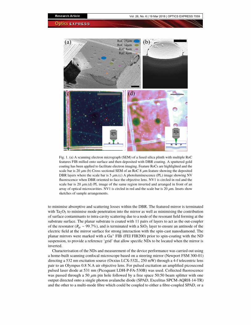
Fig. 1. (a) A scanning electron micrograph (SEM) of a fused silica plinth with multiple RoCfeatures FIB milled onto surface and then deposited with DBR coating. A sputtered goldcoating has been applied to facilitate electron imaging. Feature RoCs are highlighted and thescale bar is 20 µm (b) Cross sectional SEM of an RoC 8 µm feature showing the depositedDBR layers where the scale bar is 5 µm.(c) A photoluminescence (PL) image showing NVfluorescence when DBR oriented to face the objective lens. NV1 is circled in red and thescale bar is 20 µm.(d) PL image of the same region inverted and arranged in front of anarray of optical microcavities. NV1 is circled in red and the scale bar is 20 µm. Insets showsketches of sample arrangements.
to minimise absorptive and scattering losses within the DBR. The featured mirror is terminatedwith Ta2O5 to minimise mode penetration into the mirror as well as minimising the contributionof surface contaminants to intra-cavity scattering due to a node of the resonant field forming at thesubstrate surface. The planar substrate is coated with 11 pairs of layers to act as the out-couplerof the resonator (Rp ∼ 99.7%), and is terminated with a SiO2 layer to ensure an antinode of theelectric field at the mirror surface for strong interaction with the spin-cast nanodiamond. Theplanar mirrors were marked with a Ga+ FIB (FEI FIB200) prior to spin-coating with the NDsuspension, to provide a reference ‘grid’ that allow specific NDs to be located when the mirror isinverted.
Characterisation of the NDs and measurement of the device performance was carried out usinga home-built scanning confocal microscope based on a steering mirror (Newport FSM 300-01)directing a 532 nm excitation source (Oxxius LCX-532L, 250 mW) through a 4-f telecentric lenspair to an Olympus 0.8 N.A air objective lens. For pulsed excitation an amplified picosecondpulsed laser diode at 531 nm (Picoquant LDH-P-FA-530B) was used. Collected fluorescencewas passed through a 50 µm pin hole followed by a free space 50:50 beam splitter with oneoutput directed onto a single photon avalanche diode (SPAD, Excelitas SPCM-AQRH-14-TR)and the other to a multi-mode fibre which could be coupled to either a fibre-coupled SPAD, or a
Vol. 26, No. 6 | 19 Mar 2018 | OPTICS EXPRESS 7059
spectrometer.To identify suitable single NV centres for cavity coupling, fluorescence from the spin-cast
nanodiamonds on the planar mirror is first imaged as shown in figure 1(c). Peaks in intensity areidentified by an image processing script and an automatic sequence conducts Hanbury Brown andTwiss (HBT) interferometry on each. This was found to be an effective way to both photo-bleachunstable features, and allow the remaining peaks to be rapidly assayed to identify strong and stablesingle photon emitters. The fluorescence saturation intensity and saturation excitation power (Isat& Psat respectively) were measured for each of these selected NV centres, and the orientation oftheir axis of symmetry found by rotating the excitation polarisation. The polarisation state of theemitted photons was not investigated during this study however the TEM00 for the cavities usedhere is degenerate for orthogonal polarisation states, and so the polarisation properties of theNV centre’s emission are thought to be unaffected by its coupling to these cavity modes. Thefluorescence spectrum was recorded to ensure that the NV centre remained predominantly in thenegative charge state. Time-correlated single photon counting yields the excited state lifetimethrough time-resolved photoluminescence (TRPL), and HBT measurements were performed withpulsed excitation to establish the single photon emission fidelity.
Once the selected NVs have been fully characterised, the planar mirror is inverted and the sameNV centres relocated using the registration marks, allowing a concave mirror to be positionedbehind a chosen NV as shown in figure 1(d). The cavity coupling and tuning is then achieved byreducing the cavity length with a piezoelectric actuator. The plano-concave resonators displayHermite-Gauss mode structure, denoted by TEMnm, where n and m are the orders of the Hermitepolynomials describing the field distribution in the x and y directions respectively.
3. Results and analysis
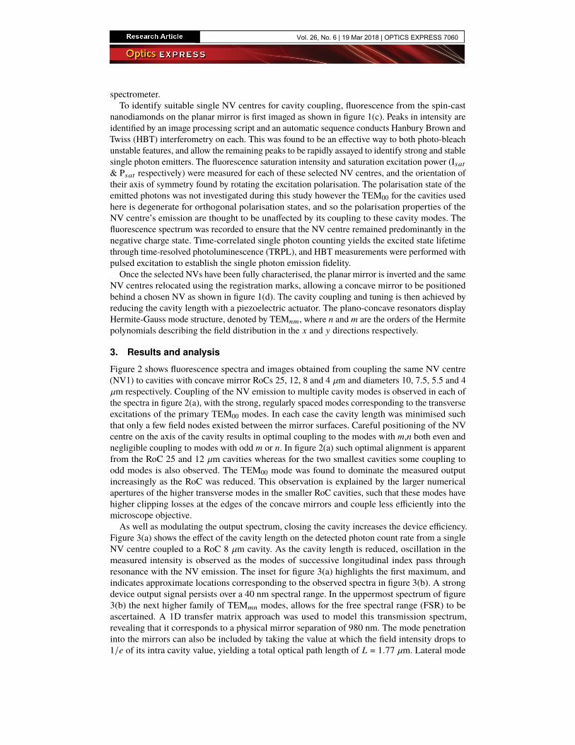
Figure 2 shows fluorescence spectra and images obtained from coupling the same NV centre(NV1) to cavities with concave mirror RoCs 25, 12, 8 and 4 µm and diameters 10, 7.5, 5.5 and 4µm respectively. Coupling of the NV emission to multiple cavity modes is observed in each ofthe spectra in figure 2(a), with the strong, regularly spaced modes corresponding to the transverseexcitations of the primary TEM00 modes. In each case the cavity length was minimised suchthat only a few field nodes existed between the mirror surfaces. Careful positioning of the NVcentre on the axis of the cavity results in optimal coupling to the modes with m,n both even andnegligible coupling to modes with odd m or n. In figure 2(a) such optimal alignment is apparentfrom the RoC 25 and 12 µm cavities whereas for the two smallest cavities some coupling toodd modes is also observed. The TEM00 mode was found to dominate the measured outputincreasingly as the RoC was reduced. This observation is explained by the larger numericalapertures of the higher transverse modes in the smaller RoC cavities, such that these modes havehigher clipping losses at the edges of the concave mirrors and couple less efficiently into themicroscope objective.
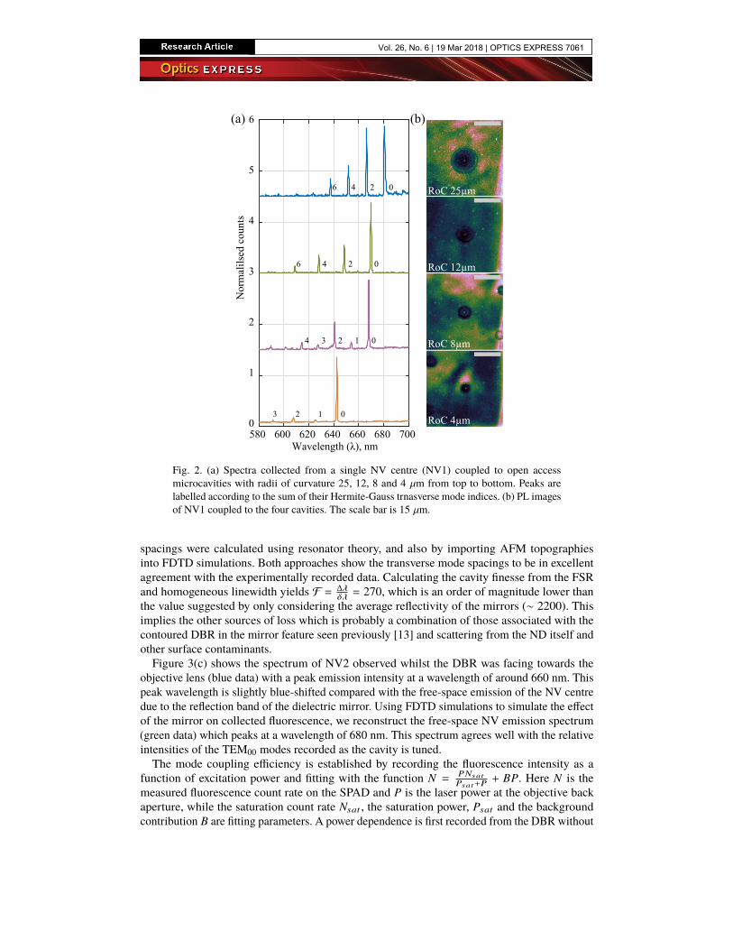
As well as modulating the output spectrum, closing the cavity increases the device efficiency.Figure 3(a) shows the effect of the cavity length on the detected photon count rate from a singleNV centre coupled to a RoC 8 µm cavity. As the cavity length is reduced, oscillation in themeasured intensity is observed as the modes of successive longitudinal index pass throughresonance with the NV emission. The inset for figure 3(a) highlights the first maximum, andindicates approximate locations corresponding to the observed spectra in figure 3(b). A strongdevice output signal persists over a 40 nm spectral range. In the uppermost spectrum of figure3(b) the next higher family of TEMmn modes, allows for the free spectral range (FSR) to beascertained. A 1D transfer matrix approach was used to model this transmission spectrum,revealing that it corresponds to a physical mirror separation of 980 nm. The mode penetrationinto the mirrors can also be included by taking the value at which the field intensity drops to1/e of its intra cavity value, yielding a total optical path length of L = 1.77 µm. Lateral mode
Vol. 26, No. 6 | 19 Mar 2018 | OPTICS EXPRESS 7060
RoC 25µm
RoC 4µm
RoC 12µm
RoC 8µm
Wavelength (λ), nm580 600 620 640 660 680 700
Nor
mal
ilsed
cou
nts
0
1
2
3
4
5
6(a) (b)
0
0
0
02
2
2
2
4
4
4
6
6
1
1
3
3
Fig. 2. (a) Spectra collected from a single NV centre (NV1) coupled to open accessmicrocavities with radii of curvature 25, 12, 8 and 4 µm from top to bottom. Peaks arelabelled according to the sum of their Hermite-Gauss trnasverse mode indices. (b) PL imagesof NV1 coupled to the four cavities. The scale bar is 15 µm.
spacings were calculated using resonator theory, and also by importing AFM topographiesinto FDTD simulations. Both approaches show the transverse mode spacings to be in excellentagreement with the experimentally recorded data. Calculating the cavity finesse from the FSRand homogeneous linewidth yields F = ∆λδλ = 270, which is an order of magnitude lower thanthe value suggested by only considering the average reflectivity of the mirrors (∼ 2200). Thisimplies the other sources of loss which is probably a combination of those associated with thecontoured DBR in the mirror feature seen previously [13] and scattering from the ND itself andother surface contaminants.Figure 3(c) shows the spectrum of NV2 observed whilst the DBR was facing towards the
objective lens (blue data) with a peak emission intensity at a wavelength of around 660 nm. Thispeak wavelength is slightly blue-shifted compared with the free-space emission of the NV centredue to the reflection band of the dielectric mirror. Using FDTD simulations to simulate the effectof the mirror on collected fluorescence, we reconstruct the free-space NV emission spectrum(green data) which peaks at a wavelength of 680 nm. This spectrum agrees well with the relativeintensities of the TEM00 modes recorded as the cavity is tuned.The mode coupling efficiency is established by recording the fluorescence intensity as a
function of excitation power and fitting with the function N = PNsat
Psat+P+ BP. Here N is the
measured fluorescence count rate on the SPAD and P is the laser power at the objective backaperture, while the saturation count rate Nsat , the saturation power, Psat and the backgroundcontribution B are fitting parameters. A power dependence is first recorded from the DBR without
Vol. 26, No. 6 | 19 Mar 2018 | OPTICS EXPRESS 7061
580 600 620 640 660 680 700
A.u
.
Wavelength (λ), nm
600 640 680 720
A.u
Wavelength (λ), nm
(a) (b)
(c) Cavity length, nm
620 660 700
1000 1200 1400 1600 1800 20001
2
3
4
5
Cou
nts x
104 p
er se
cond
1000 1200
l = 3
l = 4
l = 5
l = 6
Fig. 3. (a) Enhanced photon count rates for a RoC 8 µm feature closed around NV2.Peak labels show the number of field antinodes between the mirrors. The inset shows theapproximate cavity lengths of spectra shown in (b). (b) Collected spectra at several pointsobserved by tuning the cavity length over the intensity maximum in a). Note that the linewidths shown here are inhomogeneously broadened by spectral drift over the integration time.(c) Observed emission spectrum of NV2 prior to cavity coupling (blue), and inferred emissionspectrum of NV2 after removing the effect of the DBR mirror using FDTD (green). TEM00modes (red), show agreement in phonon sideband maximum and optimum fluorescencecollection rates.
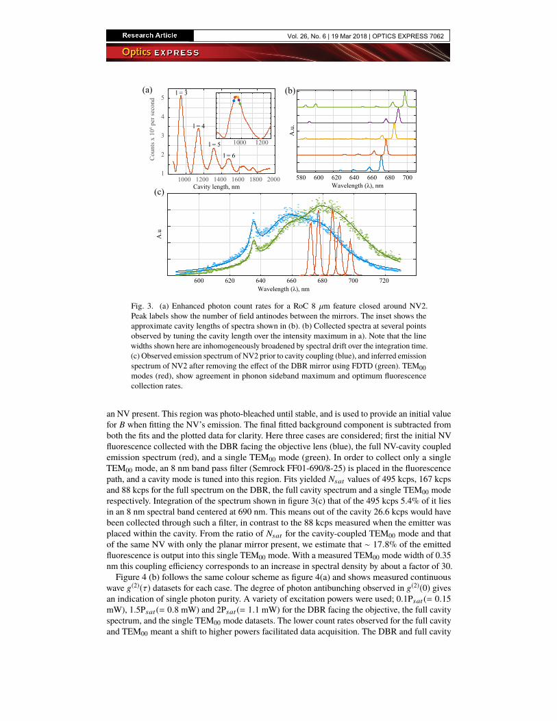
an NV present. This region was photo-bleached until stable, and is used to provide an initial valuefor B when fitting the NV’s emission. The final fitted background component is subtracted fromboth the fits and the plotted data for clarity. Here three cases are considered; first the initial NVfluorescence collected with the DBR facing the objective lens (blue), the full NV-cavity coupledemission spectrum (red), and a single TEM00 mode (green). In order to collect only a singleTEM00 mode, an 8 nm band pass filter (Semrock FF01-690/8-25) is placed in the fluorescencepath, and a cavity mode is tuned into this region. Fits yielded Nsat values of 495 kcps, 167 kcpsand 88 kcps for the full spectrum on the DBR, the full cavity spectrum and a single TEM00 moderespectively. Integration of the spectrum shown in figure 3(c) that of the 495 kcps 5.4% of it liesin an 8 nm spectral band centered at 690 nm. This means out of the cavity 26.6 kcps would havebeen collected through such a filter, in contrast to the 88 kcps measured when the emitter wasplaced within the cavity. From the ratio of Nsat for the cavity-coupled TEM00 mode and thatof the same NV with only the planar mirror present, we estimate that ∼ 17.8% of the emittedfluorescence is output into this single TEM00 mode. With a measured TEM00 mode width of 0.35nm this coupling efficiency corresponds to an increase in spectral density by about a factor of 30.Figure 4 (b) follows the same colour scheme as figure 4(a) and shows measured continuous
wave g(2)(τ) datasets for each case. The degree of photon antibunching observed in g(2)(0) givesan indication of single photon purity. A variety of excitation powers were used; 0.1Psat (= 0.15mW), 1.5Psat (= 0.8 mW) and 2Psat (= 1.1 mW) for the DBR facing the objective, the full cavityspectrum, and the single TEM00 mode datasets. The lower count rates observed for the full cavityand TEM00 meant a shift to higher powers facilitated data acquisition. The DBR and full cavity
Vol. 26, No. 6 | 19 Mar 2018 | OPTICS EXPRESS 7062
-300 -200 -100 0 100 200 300
Nor
mal
ised
cou
nts
0
0.2
0.4
0.6
0.8
1
Time (τ), ns
Power, mW
Cts
x 1
05 /s
0
0.5
1
1.5
2
2.5
3
3.5
4
0 1 2 3 4 5 -200 -150 -100 -50 0
Seco
nd o
rder
cor
rela
tion,
g2 (τ
)
0
0.5
1
1.5
2
2.5
3
3.5
Time (τ), ns
-100 10010-2
10-1
100
0
TEM00
All modes
DBR
All modes
TEM00
DBR
(a) (b)
(c) (d)
Time (τ), ns 50
Nor
mal
ilsed
cts
10-2
10-1
100
-50 0 50-50 0 50-50 0
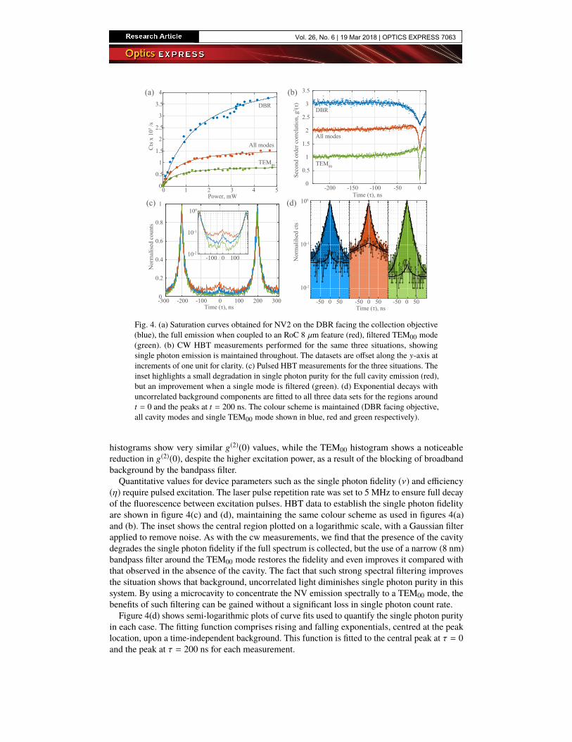
Fig. 4. (a) Saturation curves obtained for NV2 on the DBR facing the collection objective(blue), the full emission when coupled to an RoC 8 µm feature (red), filtered TEM00 mode(green). (b) CW HBT measurements performed for the same three situations, showingsingle photon emission is maintained throughout. The datasets are offset along the y-axis atincrements of one unit for clarity. (c) Pulsed HBT measurements for the three situations. Theinset highlights a small degradation in single photon purity for the full cavity emission (red),but an improvement when a single mode is filtered (green). (d) Exponential decays withuncorrelated background components are fitted to all three data sets for the regions aroundt = 0 and the peaks at t = 200 ns. The colour scheme is maintained (DBR facing objective,all cavity modes and single TEM00 mode shown in blue, red and green respectively).
histograms show very similar g(2)(0) values, while the TEM00 histogram shows a noticeablereduction in g(2)(0), despite the higher excitation power, as a result of the blocking of broadbandbackground by the bandpass filter.
Quantitative values for device parameters such as the single photon fidelity (ν) and efficiency(η) require pulsed excitation. The laser pulse repetition rate was set to 5 MHz to ensure full decayof the fluorescence between excitation pulses. HBT data to establish the single photon fidelityare shown in figure 4(c) and (d), maintaining the same colour scheme as used in figures 4(a)and (b). The inset shows the central region plotted on a logarithmic scale, with a Gaussian filterapplied to remove noise. As with the cw measurements, we find that the presence of the cavitydegrades the single photon fidelity if the full spectrum is collected, but the use of a narrow (8 nm)bandpass filter around the TEM00 mode restores the fidelity and even improves it compared withthat observed in the absence of the cavity. The fact that such strong spectral filtering improvesthe situation shows that background, uncorrelated light diminishes single photon purity in thissystem. By using a microcavity to concentrate the NV emission spectrally to a TEM00 mode, thebenefits of such filtering can be gained without a significant loss in single photon count rate.
Figure 4(d) shows semi-logarithmic plots of curve fits used to quantify the single photon purityin each case. The fitting function comprises rising and falling exponentials, centred at the peaklocation, upon a time-independent background. This function is fitted to the central peak at τ = 0and the peak at τ = 200 ns for each measurement.
Vol. 26, No. 6 | 19 Mar 2018 | OPTICS EXPRESS 7063
Time (τ), ns0 100 120 140
Nor
mal
ised
cou
nts
10-2
10-1
100
20 40 60 80
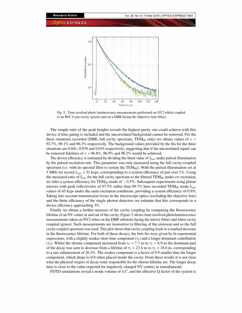
Fig. 5. Time resolved photo luminescence measurements performed on NV2 whilst coupledto an RoC 8 µm cavity (green) and on a DBR facing the objective lens (blue).
The simple ratio of the peak heights reveals the highest purity one could achieve with thisdevice if time gating is included and the uncorrelated background cannot be removed. For thethree situations recorded (DBR, full cavity spectrum, TEM00 only) we obtain values of ν =92.7%, 89.1% and 96.3% respectively. The background values provided by the fits for the threesituations are 0.041, 0.078 and 0.019 respectively, suggesting that if the uncorrelated signal canbe removed fidelities of ν = 96.8%, 96.9% and 98.2% would be achieved.
The device efficiency is estimated by dividing the fitted value of Isat under pulsed illuminationby the pulsed excitation rate. This parameter was only measured using the full cavity-coupledspectrum (i.e. with no spectral filter to isolate the TEM00). With the pulsed illumination set at5 MHz we record Isat = 51 kcps, corresponding to a system efficiency of just over 1%. Usingthe measured ratio of Isat for the full cavity spectrum to the filtered TEM00 under cw excitation,we infer a system efficiency for TEM00 mode of ∼ 0.5%. Subsequent experiments using planarmirrors with peak reflectivities of 97.5% rather than 99.7% have recorded TEM00 mode Isatvalues of 45 kcps under the same excitation conditions, providing a system efficiency of 0.9%.Taking into account transmission losses in the microscope optics (excluding the objective lens)and the finite efficiency of the single photon detectors we estimate that this corresponds to adevice efficiency approaching 3%.Finally we obtain a further measure of the cavity coupling by comparing the fluorescence
lifetime of an NV centre in and out of the cavity. Figure 5 shows time-resolved photoluminescencemeasurements taken on NV2 when on the DBR substrate facing the mirror (blue) and when cavitycoupled (green). Such measurements are insensitive to filtering of the emission and so the fullcavity coupled spectrumwas used. This plot shows that cavity coupling leads to a marked decreasein the fluorescence lifetime. For both of these decays, the best fits were given by bi-exponentialexpressions, with a slightly weaker short time component (τ1) and a longer dominant contribution(τ2). Whilst the shorter component increased from τ1 = 7.7 ns to τ1 = 8.9 ns the dominant partof the decay was seen to decrease from a lifetime of τ2 = 23.6 ns to τ2 = 18.6 ns, correspondingto a rate enhancement of 26.3%. The weaker component is a factor of 0.9 smaller than the longercomponent, which drops to 0.8 when placed inside the cavity. From these results it is not clearwhat the physical origins of decay route responsible for the shorter lifetime are. The longer decaytime is close to the value expected for negatively charged NV centres in nanodiamond.FDTD simulations reveal a mode volume of 4λ3, and the effective Q factor of the system is
Vol. 26, No. 6 | 19 Mar 2018 | OPTICS EXPRESS 7064
shown from 1Qe f f
= 1Qcav
+ 1Qemit
= 0.35690 +
70690 to be ≈ 10. From the usual expression for the
Purcell factor, Fp =3Qe f f
4π2V
(λn
)3, taking the refractive index of the mode to be 1 corresponding tothe air intracavity medium gives FP = 0.2 for the TEM00 mode alone, and including proportionatecontributions from the other transverse modes present in the measured spectrum in figure 2agives an effective Purcell factor of 0.3, in excellent agreement with the measured value, once theemission into non cavity modes is taken into account by adding 1. The efficiency of couplinginto the TEM00 mode of β = FP/(FP + 1) = 0.17, also in excellent agreement with the couplingefficiency measured from the comparison between the measured fluorescence intensities describedearlier.
4. Conclusions and outlook
In summary we have reported progress in the realisation of robust, room temperature triggeredsingle photon sources based on the coupling of a single NV centre in nanodiamond to openaccess microcavities with dielectric mirrors. We have demonstrated optimisation of the cavityparameters by the repeatable coupling of the same single NV centre to a series of engineeredcavity mirrors. We find that up to 17% of the room temperature emission is coupled into a singleTEM00 mode of width 0.35 nm, corresponding to an increase in spectral density by a factor of30 and demonstrating the important role that cavity feeding in the bad emitter regime can playin achieving a tunable room temperature single photon source. Single photon fidelity in excessof 96% is recorded, along with a recorded single photon device efficiency of around 3%. Suchdevice specifications hold promise for the realisation of practical triggered single photon sourcesoperating at room temperature.
Funding
European Commission (FP7 WASPS), grant agreement number 618078.
Acknowledgments
S.A. and S. J. acknowledge support from the UK Engineering and Physical Sciences ResearchCouncil. A.A.P.T. and L.F. acknowledge support from the Leverhulme Trust.
Vol. 26, No. 6 | 19 Mar 2018 | OPTICS EXPRESS 7065