Embed Size (px)
Citation preview

Robust design of delta-sigma ADC system inputs for EOS immunity – PLC analog input module
Dale Li
Applications, Data Converters – Precision ADC

• EOS and fault conditions
– EOS vs ESD
– Fault conditions
• Diode and ADC input structure
– Diode: Type and characteristic
– ADC input protection structure
• Protection topologies for RTD in PLC AI module
– Conventional TVS diode
– TI flat-clamp TVS diode
• IEC testing (IEC61000-4-x) – RTD in PLC AI module
Agenda

3
ESD vs. EOS – what’s the difference?
ESD
• Electrostatic discharge
• Short duration event (1-100ns)
• High voltage (kV)
• Fast edges
• Both “in-circuit” and “out-of-circuit”
EOS
• Electrical overstress
• Longer duration event
– Milliseconds or more
– Can be continuous
• Lower voltage
– May be just beyond absolute
maximum ratings
• “In-circuit” event only

EOS from fault or overdriven
– Fault conditions
Harsh electrical environment
High voltage circuit in the system
Improper power up sequencing
Hot-swap connection and disconnection
Loss of power supply but input signal is applied
Apply bipolar signal to unipolar input ADC
Miswiring
Other conditions violating the absolute maximum specifications
– Key conditions to result in an EOS to RTD application:
Miswiring power supply to RTD input
Connect high voltage signal from voltage channel to RTD input 4

• EOS and fault conditions
– EOS vs ESD
– Fault conditions
• Diode and ADC input structure
– Diode: Type and characteristic
– ADC input protection structure
• Protection topologies for RTD in PLC AI module
– Conventional TVS diode
– TI flat-clamp TVS diode
• IEC testing (IEC61000-4-x) – RTD in PLC AI module
Agenda

Unidirectional TVS Diode (Transient voltage suppressor)
TVS_Uni
Symbol Parameter VBR Breakdown voltage VR Stand-off voltage VC Clamping voltage VF Forward voltage drop IBR Breakdown Current @ VBR IR Reverse Leakage @ VR IF Forward Current @ VF IPP Peak Pulse current @ VC
VR
IR
IF
IBR
VBRVC
I
V
IPP
VF
6

Symbol Parameter VBR Breakdown voltage VR Stand-off voltage VC Clamping voltage VF Forward voltage drop IBR Breakdown Current @ VBR IR Reverse Leakage @ VR IF Forward Current @ VF IPP Peak Pulse current @ VC
VR
IR
IBR
VBRVC
I
V
IPP
V VBRR
IBR
RI
Bidirectional TVS diode (Transient voltage suppressor)
TVS_Bi
7

• Capacitance
– Not constant, change with standoff voltage
– Junction capacitance changes from
hundreds pF up to 10-nF
– Large power rating diode has higher
capacitance and variation
– Key impact to switch-capacitor input
structure SAR ADC
• Leakage Current
– Data sheet from most manufacturers only
shows max leakage at room temperature.
– Same PN from different manufacturers
may have different leakage spec.
– Leakage variation with temperature.
– Key impact to RTD measurement.
Capacitance and leakage current on TVS diode
Manufacturers PN Leakage current(max at 25°C)
Bourns Inc. SMBJ14CA 1uA
Littelfuse SMBJ14CA 1uA
Vishay SMBJ14CA 1uA
Diodes Inc. SMBJ14CA 5uA
Taiwan Semi SMBJ14CA 5uA
8

TVS vs. Zener
• TVS Diode
– Solid state PN junction
– Designed for operation in reverse-
breakdown region only during over-
voltage events
– Junction area sized to conduct
significant current and absorb significant
power
– Specifically designed for large transients
such as ESD
– Can react to overvoltage in pico-
seconds
• Zener
– Solid state PN junction
– Designed for full-time operation in
reverse-breakdown region
– Ideal for voltage regulation
– Slower reaction time
– Lower current/power capability
Zener diode
9

Internal clamp/protection on data converters
1. Input steering diodes: 2. Back-to-back Zener diode: 3. SCR-based input:
AIN_P
AIN_M
AVDD or VREF
ADC Core
AIN_nP
AIN_nGND
AFEADC Core
Input Clamp Protection
*Bi-directional SCR example
AIN_nP
AIN_nGND
SCR - Based ESD Protection*
ADC CoreAFE
10

• EOS and fault conditions
– EOS vs ESD
– Fault conditions
• Diode and ADC input structure
– Diode: Type and characteristic
– ADC input protection structure
• Protection topologies for RTD in PLC AI module
– Conventional TVS diode
– TI flat-clamp TVS diode
• IEC testing (IEC61000-4-x) – RTD in PLC AI module
Agenda
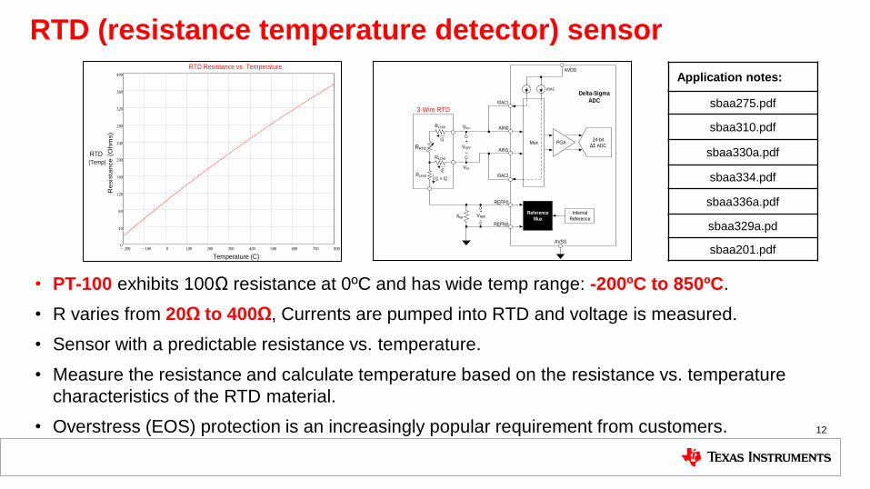
RTD (resistance temperature detector) sensor
• PT-100 exhibits 100Ω resistance at 0ºC and has wide temp range: -200ºC to 850ºC.
• R varies from 20Ω to 400Ω, Currents are pumped into RTD and voltage is measured.
• Sensor with a predictable resistance vs. temperature.
• Measure the resistance and calculate temperature based on the resistance vs. temperature
characteristics of the RTD material.
• Overstress (EOS) protection is an increasingly popular requirement from customers.
200 100 0 100 200 300 400 500 600 700 8000
40
80
120
160
200
240
280
320
360
400
RTD Resistance vs. Temperature
Temperature (C)
Re
sis
tan
ce
(O
hm
s)
RTD(Temp)
RLEAD
RLEAD
I1
I2
I1 + I2
RRTD
RLEAD
3-Wire RTD
Delta-Sigma
ADC
AIN0
AIN1
IDAC2
IDAC1
REFP0
REFN0
Reference
Mux
AVDD
AVSS
Internal
Reference
IDAC
PGA24-bit
ΔΣ ADCMux
RREF
VDIFF
–
VIN-
+
VIN+
VREF
–
+
Application notes:
sbaa275.pdf
sbaa310.pdf
sbaa330a.pdf
sbaa334.pdf
sbaa336a.pdf
sbaa329a.pd
sbaa201.pdf
12

• Differential VREF inputs
• 1x current sources
• Low-noise
• Integrated gain stage
Typical block diagram: 2-wire RTD inputs
• 2 terminal input
• High-side reference (low-side is
possible as well)
• One excitation current required
• No lead wire compensation
• RREF is typically largest source of error
2-wire RTD block diagram Circuit notes
Key ADC Specs
13
**From ADS124S08 EVM
+
Vref
-
+
VRTD
-
- Verror+
+ Verror-

• Differential VREF inputs
• 2x or 1x current sources
• Low-noise
• Integrated gain stage
Typical block diagram: 3-wire RTD inputs
• 3 terminal input
• High-side reference (low-side is
possible as well)
• Excitation via 1x or 2x current sources
(1x IDAC requires 2x measurements)
• Lead wire compensation is possible
• RREF is typically largest source of error
3-wire RTD block diagram Circuit notes
Key ADC Specs
14
**From ADS124S08 EVM
+
Vref
-
+
VRTD
-
- Verror+
+ Verror-
- 0V+

• Differential VREF inputs
• 1x current source
• Low-noise
• Integrated gain stage
Typical block diagram: 4-wire RTD Inputs
• 4 terminal input
• High-side reference (low-side is
possible as well)
• One excitation current required
• Inherent lead wire compensation
• RREF is typically largest source of error
4-wire RTD block diagram Circuit notes
Key ADC Specs
15
**From ADS124S08 EVM
+
Vref
-
+
VRTD
-
- Verror+
+ Verror-
- 0V+
- 0V+

Design dequirements
Parameter Value
Input sensor RTD: PT100
Measurement range -200ºC to 850ºC (20Ω to 400Ω)
EOS fault protection ±30V on RTD input
Resolution ENOB: >20 bits
Noise-free resolution: >17 bits
Accuracy (TA = -40 to 85°C) ±0.1% at room, ±0.5% full temp range
IEC certifications
ESD: IEC61000-4-2
EFT: IEC61000-4-4
Surge: IEC61000-4-5
16

Design block diagram: RTD measurement (IEC Testing)
Note: ADS124S08’s other channels are used for voltage and current measurement in this design.
3.3V
(IDAC)
(Optional) 3.3V
SPI
2.5V
REF
5V
3.3V
TPS7A4700 6-24V
GND 3.3V
5V
TPS7A4700
TPS7A4700 SN6505 TPS7A4700
3.3V 5V
TPS7A4700
NON-ISOLATED CIRCUIT
RTD:
4/3/2-wire
Low/High
side
2/1 IDAC
supported
TM4C1294 SPI
ISOLATED CIRCUIT
USB
RC Filter
R
C R
Protection
(EOS,
ESD,
Surge
etc.)
Protection
Protection
Rref1
Rref0
(IDAC)
24-Bit
ADC PGA
Digital
Filter
Oscillator
Calibration
8:1
Mux
AIN4
AIN2
AIN1
AIN0
AIN3
REFP0
REFN0
Serial
Interface ISO7741
AVDD AIN5 REFP1 DVDD REFN1
ADS124S08
AVDD DVDD
17

Common 3-wire RTD measurement without protection
3-wire RTD, low-side reference measurement circuit with one
IDAC current source (common-mode capacitor not shown)
• Ratiometric measurement:
IDAC noise and drift are cancelled.
• Lead wire resistance cancellation:
Lead resistance is related to length, material and
cross-sectional-area of the conductor.
One IDAC needs two measurements.
• Two IDACs need current chopping to minimize
the effect of mismatched current sources.
Note: 1-meter PT100 RTD sensor from Adafruit.
AVDD=5V
PGA
AVSS DGND
24-Bit Δ∑
ADC
ADS124S08
DVDD=3.3V
AIN2
AIN4
Mu
x
IDAC1
REFP0
RREF
IDAC2
REFN0
AIN5
AIN0
V1
V2
RLead1
RRTDRLead2
RLead3
Rflt1
Rflt2
Rflt3
Rflt4
Cflt1
Cflt2
Cflt3
Cflt4
18

Why do we need two measurements
Two measurements by taking difference
between 𝐕𝟏 and 𝐕𝟐:
Cancel lead wire resistance.
Cancel the offset of ADC.
Low side reference requires two measurements.
High side reference measurement only requires
one measurement, however the resistor
selections (RRTD, Rref and Rbias) and IDAC current
are limited by compliance voltage.
VRTD=
24-Bit Δ
ADC
IDAC1
RREF
RLead1
RRTD
RLead2
RLead3
V1=+110mV
Vref
I=1mA
-10mV++
100mV
-
- 0V +
+10mV-
Note: RRTD =100Ω, RLead1 = RLead2 = RLead3 = 10Ω
VRTD=
24-Bit Δ
ADC
IDAC1
RREF
RLead1
RRTD
RLead2
RLead3
Vref
I=1mA
-10mV++
100mV
-
- 0V +
+10mV-
V2=+10mV
Vmeas=V1-V2=100mV
19

ESD / EOS Protection Design
RP1 R1
T4
15.6V Breakdown
AVDD
5V
Vfault
+30VVfault
+14.4V-
Vfault
+9.9V-
-
0.7V
+
ADC
IABS_MAX
Design Goals
• Assume continuous fault
• Limit IABS_MAX < 10mA
• Minimize fault power
dissipation in RP1, R1, and T4
• Make sure normal operation
of circuit is functional and has
minimal error
Compliance limit
Leakage Errors

Protection: 3-wire RTD, low-side reference measurement
21
Absolute Maximum Ratings (Single 5V Power Supply)
Parameter MIN TYP MAX UNIT
Analog input voltage ( Vin_Abs) -0.3 +5.3 V
Analog input current ( Iin_Abs) -10 +10 mA
Normal input signal
AINx signal ( Vin ) 0 +5 V
• Current limiting resistors:
RP1/RP2/RP3/RP4:
limit current to TVS and ADC inputs
R1 limits current to IDAC (no Rflt on AIN5).
Large value RP1 and R1 limit current more:
- Advantage: lower clamped voltage under fault condition.
- Disadvantage: higher voltage under normal operation.
(violate compliance voltage on IDAC).
Small value RP1 and R1 limit less current, have higher
power dissipation on RP1 and R1.
Mismatching and drift affect accuracy.
• TVS diode considerations:
Proper standoff voltage(14V) -> tradeoff for RP1 and R1.
Bidirectional TVS instead of unidirectional TVS.
Leakage current is a key error contribution to accuracy.
Temp drift of leakage current affects accuracy.
(*Common-mode capacitor not shown)
Maximum
EOS: ±30V
Compliance voltage
= 4.6V max
AVDD=5V
PGA
AVSS DGND
24-Bit Δ
ADC
ADS124S08
DVDD=3.3V
AIN2
AIN4
Mu
x
IDAC1
REFP0
IDAC2
REFN0
AIN5
AIN0
RLead1
RRTDRLead2
RLead3
Rflt1
Rflt2
Rflt3
Rflt4
Cflt1
Cflt2
Cflt3
Cflt4
RP1
RP2
RP3
RP4
RP5
R1
T1 T4T2 T3
T5 RREF
V2
V1
Maximum
EOS: ±30 V

• Voltage drop across Rp1 can not be acceptable and power dissipation on Rp1 can be a challenge.
Diodes Inc. SMBJ14CA (Bidirectional) SMBJ14A (Unidirectional)
𝑽𝑩 (Breakdown Voltage) −15.6𝑉 − 0.7𝑉
𝑽𝑹𝑷 = 𝑉𝐸𝑂𝑆 − 𝑉𝐵 (Volts on RP) −14.4𝑉 −29.3𝑉
𝑷𝑷 =𝑉𝑅𝑃
2
𝑅𝑃1 (Power Dissipation on Rp)
(−14.4𝑉)2
590Ω= 0.351𝑊
(−29.3𝑉)2
590Ω= 𝟏. 𝟒𝟓𝟓𝑾
Why do we use bidirectional TVS diode?
VEOS: - 30V
ADS124S08
AIN2
AIN4
AIN5
AIN0
RLead1
RRTDRLead2
RLead3
Rflt1
Rflt2
Rflt3
Cflt1
Cflt2
Cflt3
R1
T4
IIDAC
RP1
RP2
RP3
RP4
SMBJ14CA
-14.4V+
VB= -15.6VVRP VEOS: - 30V
SMBJ14A
RRTD ADS124S08
AIN2
AIN4
AIN5
AIN0
RLead1
RLead2
RLead3
Rflt1
Rflt2
Rflt3
Cflt1
Cflt2
Cflt3
R1
T4
IIDAC
RP1
RP2
RP3
RP4
-29.3V+
VB= -0.7VVRP
22

Solution 1: Choose Rp1 and R1 with regular TVS diode
Part
number MFG
Reverse
standoff
voltage(VR)
Breakdown
voltage (VBR) Clamping
voltage max
(VC@IPP)
Reverse
leakage max
(IR@VR) 25°C
Breakdown
current
(IBR@VBR)
Peak pulse
current
(IPP)
Peak power
dissipation
(PPP)
Steady state
power
dissipation(PPP) Min Max
SMBJ14CA Bourns 14V 15.6 17.9 23.2V 1uA 1mA 25.9A 600W 5W
1 𝑅𝑃1 ≥𝑉𝐸𝑂𝑆_𝑚𝑎𝑥 − 𝑉𝐵𝑅_𝑚𝑖𝑛
𝐼𝑓𝑎𝑢𝑙𝑡=
30𝑉 − 15.6𝑉
25𝑚𝐴= 576Ω (𝒄𝒉𝒐𝒐𝒔𝒆 𝟓𝟗𝟎𝜴)
2 𝑅1 ≥𝑉𝐵𝑅_𝑚𝑖𝑛 − 𝑉𝑖𝑛_𝑚𝑎𝑥
𝐼𝐴𝐷𝐶=
15.6𝑉 − 5.3𝑉
5𝑚𝐴= 2.06𝑘Ω (𝒄𝒉𝒐𝒐𝒔𝒆 𝟐. 𝟐𝒌𝜴, 5𝑚𝐴 < 𝐼𝐴in_A𝑏𝑠)
Positive EOS:
(+30V)
Negative EOS:
(-30V) 1 𝑅𝑃1 ≥𝑉𝐸𝑂𝑆_𝑚𝑎𝑥 − 𝑉𝐵𝑅_𝑚𝑖𝑛
𝐼𝑓𝑎𝑢𝑙𝑡=
−30𝑉 − −15.6𝑉
−25𝑚𝐴= 576Ω (𝒄𝒉𝒐𝒐𝒔𝒆 𝟓𝟗𝟎𝜴)
2 𝑅1 ≥𝑉𝐵𝑅_𝑚𝑖𝑛 − 𝑉𝑖𝑛_𝑚𝑖𝑛
𝐼𝐴𝐷𝐶=
−15.6𝑉 − −0.3𝑉
−5𝑚𝐴= 3.06𝑘Ω (𝒄𝒉𝒐𝒐𝒔𝒆 𝟑. 𝟒𝒌𝜴, 5𝑚𝐴 < 𝐼𝐴in_A𝑏𝑠)
Power 𝑃𝑅𝑃1 =(𝑉𝐸𝑂𝑆_𝑚𝑎𝑥 − 𝑉𝐵𝑅_𝑚𝑖𝑛)2
𝑅𝑃1=
(−30𝑉 − −15.6𝑉 )2
590Ω= 351𝑚𝑊 (𝒄𝒉𝒐𝒐𝒔𝒆 ≥ 0.5𝑊 𝑓𝑜𝑟 𝑃𝑅𝑃1)
Power 𝑃𝑅1 =(𝑉𝐵𝑅_𝑚𝑖𝑛 − 𝑉𝑖𝑛_𝑚𝑖𝑛)2
𝑅1=
(−15.6𝑉 − −0.3𝑉 )2
3.4𝑘Ω= 68.85𝑚𝑊
Power 𝑃𝑇𝑉𝑆𝑚𝑎𝑥 = (𝑉𝐸𝑂𝑆_𝑚𝑎𝑥 − 𝑉𝐵𝑅_𝑚𝑖𝑛
𝑅𝑃1−
𝑉𝐵𝑅_𝑚𝑖𝑛 − 𝑉𝑖𝑛_𝑚𝑎𝑥
𝑅1) ∙ 𝑉𝐶 = (
−30𝑉 − (−15.6𝑉)
590Ω−
−15.6𝑉 − (−0.3𝑉)
3.4𝑘Ω) ∙ 23.2𝑉 = 461𝑚𝑊
Select
worst
case!
23

Select reference resistor - RREF
Parameters known:
PT100 Min (-200°C) Max (+850°C)
20Ω 400Ω *
Lead
resistance
Min Max
0Ω 10Ω
Components selected: RP = 590Ω,R1 = 3.4kΩ
Select RREF regarding maximum voltage across RRTD:
1 Use IDAC = 0.5mA (lower sensor self-heating: 0.093mW<0.1mW)
2 VRTD_max = IIDAC·RRTD_max = 0.5mA·400Ω = 0.2V
3 Use Gain = 4, VREF_min = VRTD_max·Gain = 0.2V·4 = 0.8V
=> VREF= 1V
4 RREF = VREF/IIDAC = 1V/0.5mA = 2kΩ
* Approximate value.
IIDAC
IIDAC
IIDAC
AVDD=5V
PGA
AVSS DGND
24-Bit Δ
ADC
ADS124S08
DVDD=3.3V
AIN2
AIN4
Mu
x
IDAC1
REFP0
IDAC2
REFN0
AIN5
AIN0
RLead1
RRTDRLead2
RLead3
Rflt1
Rflt2
Rflt3
Rflt4
Cflt1
Cflt2
Cflt3
Cflt4
R1
T1 T4T2 T3
T5 RREF
RP1
RP2
RP3
RP4
RP5
(*Common-mode capacitor not shown) 24

Compliance Voltage on Iref
5V – 0.4V = 4.6V
Need to confirm that
IDAC input < 4.6V

IIDAC
IIDAC
IIDAC
AVDD=5V
PGA
AVSS DGND
24-Bit Δ
ADC
ADS124S08
DVDD=3.3V
AIN2
AIN4
Mu
x
IDAC1
REFP0
IDAC2
REFN0
AIN5
AIN0
RLead1
RRTDRLead2
RLead3
Rflt1
Rflt2
Rflt3
Rflt4
Cflt1
Cflt2
Cflt3
Cflt4
R1
T1 T4T2 T3
T5 RREF
RP1
RP2
RP3
RP4
RP5
Verify node voltage
Parameters Known:
PT100 (max) 400Ω
Lead Resistance (max) 10Ω
Excitation Current (IDAC) 0.5mA
Compliance voltage (VC) 0.4V< VC< 4.6V *
V(AINx) (Gain=4) 0.45V< V AINx <4.55V *
Components Selected:
RP = 590Ω, R1 = 3.4kΩ, RREF= 2kΩ
Verify Node Voltage under Normal Operation:
VAIN5 = IIDAC·(R1 + RP1 + Rlead1 + RRTD + Rlead3 +RP5 +RREF) = 0.5mA·(3.4kΩ + 590Ω + 10Ω + 400Ω + 10Ω + 590Ω + 2kΩ) = 𝟑. 𝟑𝟓V < 4.6V ∗
* Limit calculated under specified conditions(Gain=4, AVDD=5V).
(*Common-mode capacitor not shown)
Compliance
voltage=4.6V max
26

Select Rflt and Cflt for differential and common-mode filter
ADS124S08
REFN0
REFP0
AIN4
AIN2
RLead1
RRTD
RLead2
RLead3
RREF
AIN0
Rflt
Rflt
Rflt
Cflt
Cfilt_DiffCflt
Cflt
IDAC1
Cref
Rflt_ref
Cfilt_Diff
𝐅𝐨𝐫 𝐀𝐃𝐂 𝐢𝐧𝐩𝐮𝐭 𝐟𝐢𝐥𝐭𝐞𝐫𝐢𝐧𝐠:
1 𝑓𝑖𝑛_𝐷𝑖𝑓𝑓 = 1/[2 ∙ 𝜋 ∙ 𝐶𝑖𝑛𝐷𝑖𝑓𝑓∙ (𝑅𝑅𝑇𝐷 +2 ∙ 𝑅𝑓𝑙𝑡 + 𝑅𝑝)] = 3.67𝑘𝐻𝑧
2 𝑓𝑖𝑛_𝐶𝑀 = 1/[2 ∙ 𝜋 ∙ 𝐶𝑓𝑙𝑡 ∙ (𝑅𝑅𝑇𝐷 +𝑅𝑓𝑙𝑡)] = 74.9𝑘𝐻𝑧
𝐅𝐨𝐫 𝐫𝐞𝐟𝐞𝐫𝐞𝐧𝐜𝐞 𝐢𝐧𝐩𝐮𝐭 𝐟𝐢𝐥𝐭𝐞𝐫𝐢𝐧𝐠:
1 𝑓𝑅𝑒𝑓_𝑓𝑖𝑙𝑡𝑒𝑟 = 1/(2 ∙ 𝜋 ∙ 𝐶𝑟𝑒𝑓 ∙ 𝑅𝑓𝑙𝑡_𝑟𝑒𝑓) +𝑅𝑓𝑙𝑡)] = 82𝑘𝐻𝑧
(*Protection circuitry not shown)
• Keep bandwidth of differential filter ≥ 10×data rate.
• Keep differential capacitor ≥ 10× Common-mode capacitor.
• Keep input resistance < 10kΩ for proper input sampling.
• Higher resistance helps to limit current to ADC input.
• Keep resistance low on REFN0 since for single power supply.
• Set 𝑅𝑓𝑙𝑡 =𝑅𝑓𝑙𝑡_𝑟𝑒𝑓 = 4.12𝑘Ω, 𝐶𝑓𝑙𝑡=𝐶𝑟𝑒𝑓 = 470𝑝𝐹, 𝐶𝑓𝑙𝑡_𝐷𝑖𝑓𝑓 = 4.7𝑛𝐹.
*see RTD Ratiometric Measurements and Filtering Using the ADS1148 and ADS1248. 27

Calculated and simulated error with SMBJ14CA diode
I2
I1
ItI5
I3
I4
AVDD=5V
PGA
AVSS DGND
24-Bit Δ
ADC
ADS124S08
DVDD=3.3V
AIN2
AIN4
Mu
x
IDAC1
REFP0
IDAC2
REFN0
AIN5
AIN0
RLead1
RRTDRLead2
RLead3
Rflt1
Rflt2
Rflt3
Rflt4
Cflt1
Cflt2
Cflt3
Cflt4
R1
T1 T4T2 T3
T5
RREF
V2
V1
IIDAC
RP1
RP2
RP3
RP4
RP5
• TVS leakage current are added:
I3 and I4 through both RRTD and RREF.
I2 and I1 through RREF only.
• Leakage current on SMBJ14CA from Bourns:
𝐈leak = 1uA
(maximum at room temp, no spec over temp)
Additional error (maximum) at room temperature:
Accuracy desired: ±0.5%
V2 = (IDAC+I2 + I3 + I4) ∙ Rlead3 +I2 ∙ (RRP3 + Rlead2)−I1 ∙ RRP4
Ratio_Actual = (Vmeas_error∙ Gain)/VREF=((V1 − V2) ∙ Gain)/(RREF ∙ (IDAC + I1 + I2 +I3 + I4 + I5))
= (((IDAC +2I) ∙ RRTD −3I ∙ Rlead) ∙ Gain)/(RREF ∙(IDAC +5I)) = 0.795 *
Error = (Ratio_Actual−Ratio−Ideal)/Ratio−Ideal ∙ 100% = −𝟎. 𝟔𝟐𝟓%
Ratio_Ideal = (IDAC∙ RRTD∙ Gain)/(IDAC ∙ RREF)= 400Ω∙4/2kΩ =0.8
V1 = (IDAC+I3 + I4) ∙ (RRTD + Rlead1) + I3 ∙ RRP2 − I2 ∙ (RP3 + Rlead2)
* 𝑁𝑜𝑡𝑒: 𝐼1 = 𝐼2 = 𝐼3 = 𝐼4 = 𝐼5= 𝐼
(*Common-mode capacitor not shown)
28

Component mismatch - Monte Carlo simulation in TINA™-TI
Mismatch from:
• Current limiting resistors Rpx
• Leakage current on TVS diodes.
• Temperature drift on diodes and
resistors.
IS1 1u IS2 1u IS3 1u IS4 1u
RP1 590
R1 3.4k
AIN5-IDAC1
IDAC 500u
AIN4
AIN2
AIN0
R2 4.12k
R3 4.12k
R4 4.12k
RP2 590
RP3 590
RP4 590
Rlead1 10
Rlead2 10
Rlead3 10
V+
V1
V+
V2
PT
100 -
400
RP5 590
IS5 1u Rre
f 2k
REFN0
REFP0
V+
V3
R5 4.12k
-
+
-
+
VCVS1 1
-
+
-
+
VCVS2 1 -
+
-
+
VCVS3 1
-
+
-
+
VCVS4 3.96
Vactual_ratio
-
+
-
+
VCVS5 125 Error
V4 800m
Vmeas_error
29

Component Mismatch - Monte Carlo Simulation - Cont’d
Press draw to get a graph of the histogram
𝑇𝑦𝑝𝐸𝑟𝑟𝑜𝑟 =𝑠𝑡𝑎𝑛𝑑𝑎𝑟𝑑 𝑑𝑒𝑣𝑖𝑎𝑡𝑖𝑜𝑛
𝑀𝑒𝑎𝑛∙ 100 =
276.44474𝑢
−618.861022𝑚∙ 100 = ±0.045% For 68.26% of the population
𝑀𝑎𝑥𝐸𝑒𝑟𝑟𝑜𝑟 = 3 ∙ 𝑇𝑦𝑝𝑖𝑐𝑎𝑙 = 3 ∙ ±0.045% = ±0.135% For 99.73% of the population

Error with low leakage current of TVS diode
Part number MFG
Reverse
standoff
voltage
(VR)
Breakdown
voltage (VBR) Clamping
voltage
max
(VC@IPP)
Reverse leakage (IR@VR) Peak power dissipation
W (PPP)
Typ at
27°C Max at 27°C Max at 85°C 8/20us 1ms Min Typ
TVS1401 TI 14V 17.1 17.6 22.2 1.1nA 30nA 260nA 600 120
SMBJ14CA Bourns 14V 15.6 17.2 23.2 1uA 600
Note: The error with TVS1401 at room temp is much smaller. Leakage Current vs Temperature at ±14V on TVS1401.
RTD system error calculated from leakage current:
PN MFG Error Temperature
TVS1401 TI -0.16% 85°C
SMBJ14CA Bourns -0.625% 25°C
Accuracy
desired:
±0.5%

RTD measurement: accuracy vs. temperature
RTD - 100ohm (0°C) RTD - 400ohm (850°C)
Conditions: 0.1% 10ppm/°C resistors for Rp and R1, 0.01%, 5ppm/°C resistor for Rref.
-0.05
-0.04
-0.03
-0.02
-0.01
0
0.01
0.02
0.03
0.04
0.05
-40 -20 0 20 40 60 80
Accuracy %
Temperature (C)
TVS1401 SMBJ14CA
-0.05
-0.04
-0.03
-0.02
-0.01
0
0.01
0.02
0.03
0.04
0.05
-40 -20 0 20 40 60 80
Accuracy %
Temperature (C)
TVS1401 SMBJ14CA
32
10x better than
expected!

EOS protection verification on ADC input
60Vpp
Input Signal Clamped Signal on ADC Input
33

• EOS and fault conditions
– EOS vs ESD
– Fault conditions
• Diode and ADC input structure
– Diode: Type and characteristic
– ADC input protection structure
• Protection topologies for RTD in PLC AI module
– Conventional TVS diode
– TI flat-clamp TVS diode
• IEC testing (IEC61000-4-x) – RTD in PLC AI module
Agenda

Electromagnetic compatibility (EMC) tests
IEC – International Electrotechnical Commission
• Promotes international cooperation on standardization
• Created test standards for electronics
• IEC 61000-4 standard
– IEC 61000-4-2: Electrostatic discharge (ESD)
– IEC 61000-4-3: Radiated electromagnetic interference (EMI)
– IEC 61000-4-4: Electrical fast transients (EFT)
– IEC 61000-4-5: Surge
– IEC 61000-4-6: Conducted electromagnetic interference (EMI)
* Precision Labs - Op Amps: Electrical Overstress 35

Electrical fast transient (EFT) immunity
IEC61000-4-4
Simulates everyday switching transients
caused by interruption of inductive loads,
relay bounces, etc.
* Precision Labs - Op Amps: Electrical Overstress 36

IEC 61000-4-4 threat levels
Power supply port I/O, signal, data &
control lines
Level Open-circuit
voltage (kV)
Short-circuit
current (A)
Open-circuit
voltage (kV)
Short-circuit
current (A)
1 0.5 10 0.25 5
2 1 20 0.5 10
3 2 40 1 20
4 4 80 2 40
* Precision Labs - Op Amps: Electrical Overstress 37

IEC 61000-4 test setup – RTD hardware
ESD EFT
38

Standard Type Level Outcome Grade
ESD Immunity IEC 61000-4-2 Contact ±8kV Passed Class B
Air ±15kV Passed Class B
EFT Immunity IEC 61000-4-4 5kHz ±4kV Passed Class B
100kHz ±4kV Planning
Surge Immunity IEC 61000-4-5 Planning
IEC61000-4 tested RTD module with TVS1401 EOS protection solution
39

TI Precision Labs – ADCs: Electrical Overstress on Data Converters
https://training.ti.com/eos-and-esd-adc?cu=1128375
Thank you!
Special thanks to:
Art Kay
Collin Wells
Bob Benjamin
Bryan Lizon
from PADC team
40

SLYP726

IMPORTANT NOTICE AND DISCLAIMER
TI PROVIDES TECHNICAL AND RELIABILITY DATA (INCLUDING DATASHEETS), DESIGN RESOURCES (INCLUDING REFERENCE DESIGNS), APPLICATION OR OTHER DESIGN ADVICE, WEB TOOLS, SAFETY INFORMATION, AND OTHER RESOURCES “AS IS” AND WITH ALL FAULTS, AND DISCLAIMS ALL WARRANTIES, EXPRESS AND IMPLIED, INCLUDING WITHOUT LIMITATION ANY IMPLIED WARRANTIES OF MERCHANTABILITY, FITNESS FOR A PARTICULAR PURPOSE OR NON-INFRINGEMENT OF THIRD PARTY INTELLECTUAL PROPERTY RIGHTS.These resources are intended for skilled developers designing with TI products. You are solely responsible for (1) selecting the appropriate TI products for your application, (2) designing, validating and testing your application, and (3) ensuring your application meets applicable standards, and any other safety, security, or other requirements. These resources are subject to change without notice. TI grants you permission to use these resources only for development of an application that uses the TI products described in the resource. Other reproduction and display of these resources is prohibited. No license is granted to any other TI intellectual property right or to any third party intellectual property right. TI disclaims responsibility for, and you will fully indemnify TI and its representatives against, any claims, damages, costs, losses, and liabilities arising out of your use of these resources.TI’s products are provided subject to TI’s Terms of Sale (www.ti.com/legal/termsofsale.html) or other applicable terms available either on ti.com or provided in conjunction with such TI products. TI’s provision of these resources does not expand or otherwise alter TI’s applicable warranties or warranty disclaimers for TI products.
Mailing Address: Texas Instruments, Post Office Box 655303, Dallas, Texas 75265Copyright © 2020, Texas Instruments Incorporated