Embed Size (px)
Citation preview
Invited paper Roadmap for SiC power devicesMietek Bakowski
Abstract — Silicon carbide (SiC) power devices offer signi-ficant benefits of improved efficiency, dynamic performanceand reliability of electronic and electric systems. The chal-lenges and prospects of SiC power device development are re-viewed considering different device types. A close correlationbetween an exponential increase of current handling capabilityduring recent five years and improvement in substrate qualityis demonstrated. The voltage range of silicon and SiC unipolarand bipolar power devices with respect to the on-state voltageis determined based on device simulation. 4H-SiC unipolardevices are potentially superior to all silicon devices up to10 kV. 4H-SiC unipolar devices are superior to all SiC bipolardevices up to 8÷9 kV. The low end of SiC unipolar devices isdetermined to be around 200 V provided substrate resistanceis reduced by thinning the substrate down to 100 µm. Theinfluence of reduced channel mobility on the specific on-stateresistance of 4H-SiC DMOSFETs and UMOSFETs is shown.It has been demonstrated that 6H-SiC DMOSFETs could bea better choice compared to 4H-SiC MOSFETs in the voltagerange below 600 V utilising better channel mobility obtainableso far on 6H-SiC polytype. An impact of super junction (SJ)concept on silicon and SiC MOSFET specific on-resistancelimits is demonstrated.
Keywords — SiC power devices, roadmap for, status, develop-ment trends, unipolar and bipolar SiC devices, super junctiondevices, applications, system benefits, current handling capabi-lity, simulations.
1. Introduction
Silicon carbide is an example of a so-called wide band gapsemiconductor, a material whose electronic and physicalproperties promise a major qualitative leap in semiconduc-tor device performance. Intense research and developmenthas been going on throughout the last decade in many cen-tres over the world. In particular, activities in Sweden havebeen at the forefront of development. The beginning of thenew century represents the threshold for commercialisationof SiC based devices. A number of companies are announ-cing the release of products and the number of materialproducers has multiplied four-fold.
2. Applications of power devices
Emerging WBG (wide band gap) semiconductor devices,of which silicon carbide is currently the most mature, facea well-established market of power electronics practicallytotally dominated by silicon devices. Silicon carbide powerdevices have high potential of finding its way into the main-stream applications and of capturing important parts of themarket thanks to the specific material properties of SiCthat translate into high value added for electronic power
systems. Specifically high electric field breakdown in com-bination with reasonably high electron mobility and highthermal conductivity translate into improved efficiency, dy-namic performance and reliability of electronic and electricsystems. It is relatively straightforward to envision savingson cooling requirements connected with increased work-ing temperature of the devices well above 125◦C typical ofsilicon power devices as well as reduced noise, size andweight of systems due to greatly increased operating fre-quency. To overcome both limitations has long been desiredin especially high voltage applications above 1 kV wherebipolar silicon devices must be used. Such devices are nec-essarily slow and suffer from high switching losses due tosubstantial recovery charge that makes them the limitingcomponent in terms of performance of many systems.
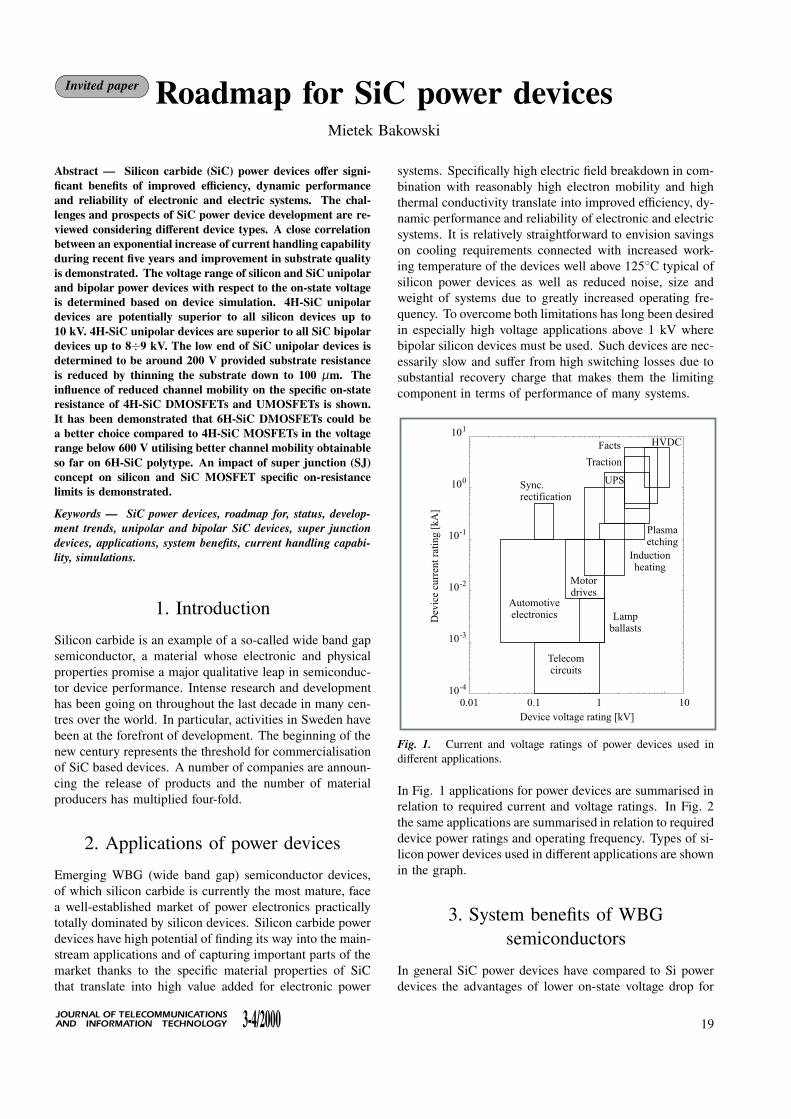
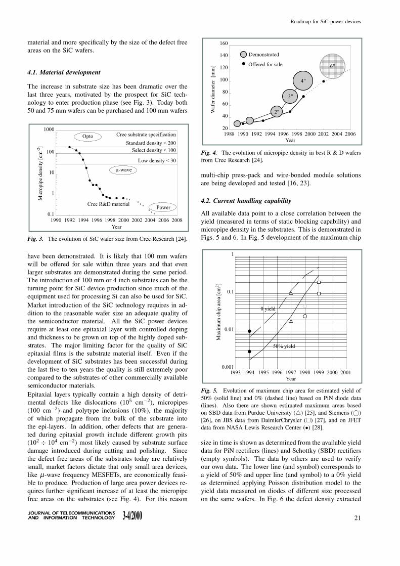
Fig. 1. Current and voltage ratings of power devices used indifferent applications.
In Fig. 1 applications for power devices are summarised inrelation to required current and voltage ratings. In Fig. 2the same applications are summarised in relation to requireddevice power ratings and operating frequency. Types of si-licon power devices used in different applications are shownin the graph.
3. System benefits of WBGsemiconductors
In general SiC power devices have compared to Si powerdevices the advantages of lower on-state voltage drop for
J O U R N AL O F T E L E CO M M U N I CAT I O N SAN D I N FO R M AT I O N T E C H N O LO GY 3-4/2000 19
Mietek Bakowski
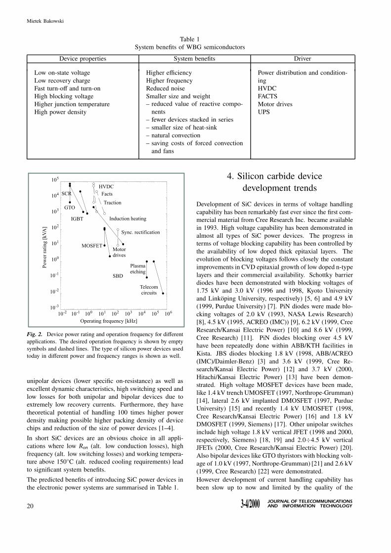
Table 1System benefits of WBG semiconductors
Device properties System benefits Driver
Low on-state voltageLow recovery chargeFast turn-off and turn-onHigh blocking voltageHigher junction temperatureHigh power density
Higher efficiencyHigher frequencyReduced noiseSmaller size and weight– reduced value of reactive compo-
nents– fewer devices stacked in series– smaller size of heat-sink– natural convection– saving costs of forced convection
and fans
Power distribution and condition-ingHVDCFACTSMotor drivesUPS
Fig. 2. Device power rating and operation frequency for differentapplications. The desired operation frequency is shown by emptysymbols and dashed lines. The type of silicon power devices usedtoday in different power and frequency ranges is shown as well.
unipolar devices (lower specific on-resistance) as well asexcellent dynamic characteristics, high switching speed andlow losses for both unipolar and bipolar devices due toextremely low recovery currents. Furthermore, they havetheoretical potential of handling 100 times higher powerdensity making possible higher packing density of devicechips and reduction of the size of power devices [1–4].
In short SiC devices are an obvious choice in all appli-cations where low Ron (alt. low conduction losses), highfrequency (alt. low switching losses) and working tempera-ture above 150◦C (alt. reduced cooling requirements) leadto significant system benefits.
The predicted benefits of introducing SiC power devices inthe electronic power systems are summarised in Table 1.
4. Silicon carbide devicedevelopment trends
Development of SiC devices in terms of voltage handlingcapability has been remarkably fast ever since the first com-mercial material from Cree Research Inc. became availablein 1993. High voltage capability has been demonstrated inalmost all types of SiC power devices. The progress interms of voltage blocking capability has been controlled bythe availability of low doped thick epitaxial layers. Theevolution of blocking voltages follows closely the constantimprovements in CVD epitaxial growth of low doped n-typelayers and their commercial availability. Schottky barrierdiodes have been demonstrated with blocking voltages of1.75 kV and 3.0 kV (1996 and 1998, Kyoto Universityand Linkoping University, respectively) [5, 6] and 4.9 kV(1999, Purdue University) [7]. PiN diodes were made blo-cking voltages of 2.0 kV (1993, NASA Lewis Research)[8], 4.5 kV (1995, ACREO (IMC)) [9], 6.2 kV (1999, CreeResearch/Kansai Electric Power) [10] and 8.6 kV (1999,Cree Research) [11]. PiN diodes blocking over 4.5 kVhave been repeatedly done within ABB/KTH facilities inKista. JBS diodes blocking 1.8 kV (1998, ABB/ACREO(IMC)/Daimler-Benz) [3] and 3.6 kV (1999, Cree Re-search/Kansai Electric Power) [12] and 3.7 kV (2000,Hitachi/Kansai Electric Power) [13] have been demon-strated. High voltage MOSFET devices have been made,like 1.4 kV trench UMOSFET (1997, Northrope-Grumman)[14], lateral 2.6 kV implanted DMOSFET (1997, PurdueUniversity) [15] and recently 1.4 kV UMOSFET (1998,Cree Research/Kansai Electric Power) [16] and 1.8 kVDMOSFET (1999, Siemens) [17]. Other unipolar switchesinclude high voltage 1.8 kV vertical JFET (1998 and 2000,respectively, Siemens) [18, 19] and 2.0÷4.5 kV verticalJFETs (2000, Cree Research/Kansai Electric Power) [20].Also bipolar devices like GTO thyristors with blocking volt-age of 1.0 kV (1997, Northrope-Grumman) [21] and 2.6 kV(1999, Cree Research) [22] were demonstrated.However development of current handling capability hasbeen slow up to now and limited by the quality of the
20J O U R N AL O F T E L E CO M M U N I CAT I O N SAN D I N FO R M AT I O N T E C H N O LO GY3-4/2000
Roadmap for SiC power devices
material and more specifically by the size of the defect freeareas on the SiC wafers.
4.1. Material development
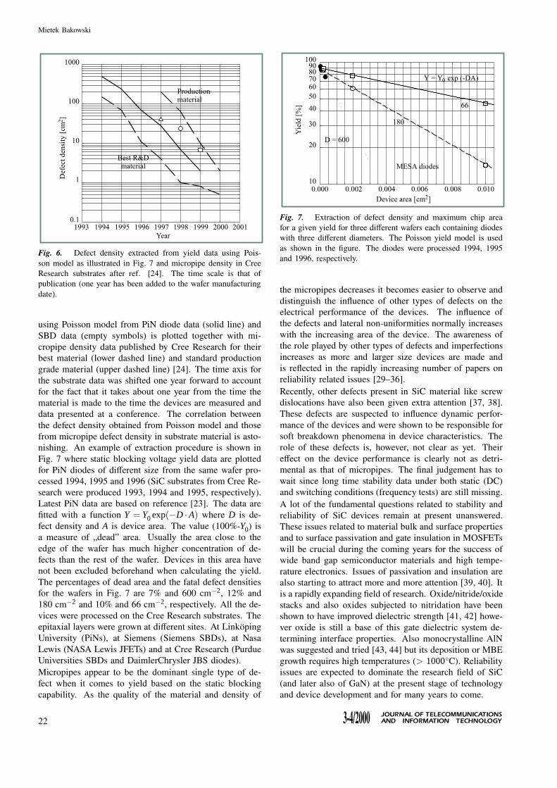
The increase in substrate size has been dramatic over thelast three years, motivated by the prospect for SiC tech-nology to enter production phase (see Fig. 3). Today both50 and 75 mm wafers can be purchased and 100 mm wafers
Fig. 3. The evolution of SiC wafer size from Cree Research [24].
have been demonstrated. It is likely that 100 mm waferswill be offered for sale within three years and that evenlarger substrates are demonstrated during the same period.The introduction of 100 mm or 4 inch substrates can be theturning point for SiC device production since much of theequipment used for processing Si can also be used for SiC.Market introduction of the SiC technology requires in ad-dition to the reasonable wafer size an adequate quality ofthe semiconductor material. All the SiC power devicesrequire at least one epitaxial layer with controlled dopingand thickness to be grown on top of the highly doped sub-strates. The major limiting factor for the quality of SiCepitaxial films is the substrate material itself. Even if thedevelopment of SiC substrates has been successful duringthe last five to ten years the quality is still extremely poorcompared to the substrates of other commercially availablesemiconductor materials.Epitaxial layers typically contain a high density of detri-mental defects like dislocations (105 cm−2), micropipes(100 cm−2) and polytype inclusions (10%), the majorityof which propagate from the bulk of the substrate intothe epi-layers. In addition, other defects that are genera-ted during epitaxial growth include different growth pits(102 ÷ 104 cm−2) most likely caused by substrate surfacedamage introduced during cutting and polishing. Sincethe defect free areas of the substrates today are relativelysmall, market factors dictate that only small area devices,like µ-wave frequency MESFETs, are economically feasi-ble to produce. Production of large area power devices re-quires further significant increase of at least the micropipefree areas on the substrates (see Fig. 4). For this reason
Fig. 4. The evolution of micropipe density in best R & D wafersfrom Cree Research [24].
multi-chip press-pack and wire-bonded module solutionsare being developed and tested [16, 23].
4.2. Current handling capability
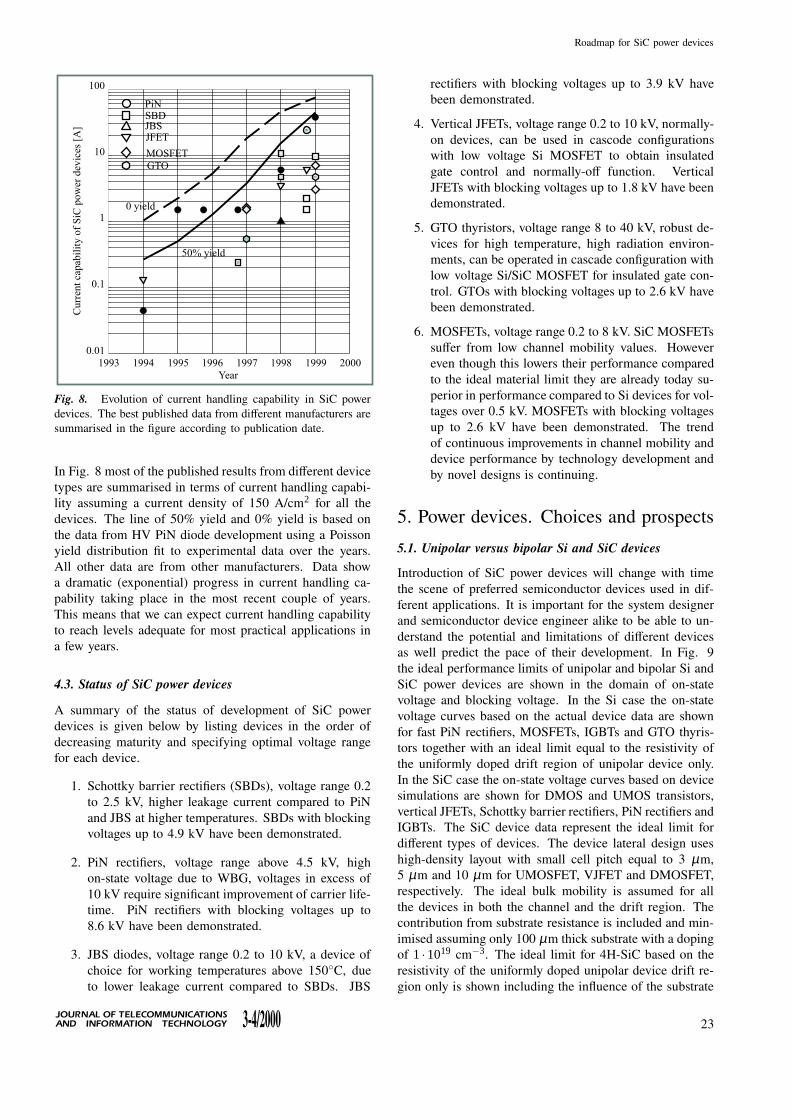
All available data point to a close correlation between theyield (measured in terms of static blocking capability) andmicropipe density in the substrates. This is demonstrated inFigs. 5 and 6. In Fig. 5 development of the maximum chip
Fig. 5. Evolution of maximum chip area for estimated yield of50% (solid line) and 0% (dashed line) based on PiN diode data(lines). Also there are shown estimated maximum areas basedon SBD data from Purdue University (4) [25], and Siemens (©)[26], on JBS data from DaimlerChrysler (�) [27], and on JFETdata from NASA Lewis Research Center (•) [28].
size in time is shown as determined from the available yielddata for PiN rectifiers (lines) and Schottky (SBD) rectifiers(empty symbols). The data by others are used to verifyour own data. The lower line (and symbol) corresponds toa yield of 50% and upper line (and symbol) to a 0% yieldas determined applying Poisson distribution model to theyield data measured on diodes of different size processedon the same wafers. In Fig. 6 the defect density extracted
J O U R N AL O F T E L E CO M M U N I CAT I O N SAN D I N FO R M AT I O N T E C H N O LO GY 3-4/2000 21
Mietek Bakowski
Fig. 6. Defect density extracted from yield data using Pois-son model as illustrated in Fig. 7 and micropipe density in CreeResearch substrates after ref. [24]. The time scale is that ofpublication (one year has been added to the wafer manufacturingdate).
using Poisson model from PiN diode data (solid line) andSBD data (empty symbols) is plotted together with mi-cropipe density data published by Cree Research for theirbest material (lower dashed line) and standard productiongrade material (upper dashed line) [24]. The time axis forthe substrate data was shifted one year forward to accountfor the fact that it takes about one year from the time thematerial is made to the time the devices are measured anddata presented at a conference. The correlation betweenthe defect density obtained from Poisson model and thosefrom micropipe defect density in substrate material is asto-nishing. An example of extraction procedure is shown inFig. 7 where static blocking voltage yield data are plottedfor PiN diodes of different size from the same wafer pro-cessed 1994, 1995 and 1996 (SiC substrates from Cree Re-search were produced 1993, 1994 and 1995, respectively).Latest PiN data are based on reference [23]. The data arefitted with a function Y = Y0 exp(−D ·A) where D is de-fect density and A is device area. The value (100%-Y0) isa measure of „dead” area. Usually the area close to theedge of the wafer has much higher concentration of de-fects than the rest of the wafer. Devices in this area havenot been excluded beforehand when calculating the yield.The percentages of dead area and the fatal defect densitiesfor the wafers in Fig. 7 are 7% and 600 cm−2, 12% and180 cm−2 and 10% and 66 cm−2, respectively. All the de-vices were processed on the Cree Research substrates. Theepitaxial layers were grown at different sites. At LinkopingUniversity (PiNs), at Siemens (Siemens SBDs), at NasaLewis (NASA Lewis JFETs) and at Cree Research (PurdueUniversities SBDs and DaimlerChrysler JBS diodes).Micropipes appear to be the dominant single type of de-fect when it comes to yield based on the static blockingcapability. As the quality of the material and density of
Fig. 7. Extraction of defect density and maximum chip areafor a given yield for three different wafers each containing diodeswith three different diameters. The Poisson yield model is usedas shown in the figure. The diodes were processed 1994, 1995and 1996, respectively.
the micropipes decreases it becomes easier to observe anddistinguish the influence of other types of defects on theelectrical performance of the devices. The influence ofthe defects and lateral non-uniformities normally increaseswith the increasing area of the device. The awareness ofthe role played by other types of defects and imperfectionsincreases as more and larger size devices are made andis reflected in the rapidly increasing number of papers onreliability related issues [29–36].Recently, other defects present in SiC material like screwdislocations have also been given extra attention [37, 38].These defects are suspected to influence dynamic perfor-mance of the devices and were shown to be responsible forsoft breakdown phenomena in device characteristics. Therole of these defects is, however, not clear as yet. Theireffect on the device performance is clearly not as detri-mental as that of micropipes. The final judgement has towait since long time stability data under both static (DC)and switching conditions (frequency tests) are still missing.A lot of the fundamental questions related to stability andreliability of SiC devices remain at present unanswered.These issues related to material bulk and surface propertiesand to surface passivation and gate insulation in MOSFETswill be crucial during the coming years for the success ofwide band gap semiconductor materials and high tempe-rature electronics. Issues of passivation and insulation arealso starting to attract more and more attention [39, 40]. Itis a rapidly expanding field of research. Oxide/nitride/oxidestacks and also oxides subjected to nitridation have beenshown to have improved dielectric strength [41, 42] howe-ver oxide is still a base of this gate dielectric system de-termining interface properties. Also monocrystalline AlNwas suggested and tried [43, 44] but its deposition or MBEgrowth requires high temperatures (> 1000◦C). Reliabilityissues are expected to dominate the research field of SiC(and later also of GaN) at the present stage of technologyand device development and for many years to come.
22J O U R N AL O F T E L E CO M M U N I CAT I O N SAN D I N FO R M AT I O N T E C H N O LO GY3-4/2000
Roadmap for SiC power devices
Fig. 8. Evolution of current handling capability in SiC powerdevices. The best published data from different manufacturers aresummarised in the figure according to publication date.
In Fig. 8 most of the published results from different devicetypes are summarised in terms of current handling capabi-lity assuming a current density of 150 A/cm2 for all thedevices. The line of 50% yield and 0% yield is based onthe data from HV PiN diode development using a Poissonyield distribution fit to experimental data over the years.All other data are from other manufacturers. Data showa dramatic (exponential) progress in current handling ca-pability taking place in the most recent couple of years.This means that we can expect current handling capabilityto reach levels adequate for most practical applications ina few years.
4.3. Status of SiC power devices
A summary of the status of development of SiC powerdevices is given below by listing devices in the order ofdecreasing maturity and specifying optimal voltage rangefor each device.
1. Schottky barrier rectifiers (SBDs), voltage range 0.2to 2.5 kV, higher leakage current compared to PiNand JBS at higher temperatures. SBDs with blockingvoltages up to 4.9 kV have been demonstrated.
2. PiN rectifiers, voltage range above 4.5 kV, highon-state voltage due to WBG, voltages in excess of10 kV require significant improvement of carrier life-time. PiN rectifiers with blocking voltages up to8.6 kV have been demonstrated.
3. JBS diodes, voltage range 0.2 to 10 kV, a device ofchoice for working temperatures above 150◦C, dueto lower leakage current compared to SBDs. JBS
rectifiers with blocking voltages up to 3.9 kV havebeen demonstrated.
4. Vertical JFETs, voltage range 0.2 to 10 kV, normally-on devices, can be used in cascode configurationswith low voltage Si MOSFET to obtain insulatedgate control and normally-off function. VerticalJFETs with blocking voltages up to 1.8 kV have beendemonstrated.
5. GTO thyristors, voltage range 8 to 40 kV, robust de-vices for high temperature, high radiation environ-ments, can be operated in cascade configuration withlow voltage Si/SiC MOSFET for insulated gate con-trol. GTOs with blocking voltages up to 2.6 kV havebeen demonstrated.
6. MOSFETs, voltage range 0.2 to 8 kV. SiC MOSFETssuffer from low channel mobility values. Howevereven though this lowers their performance comparedto the ideal material limit they are already today su-perior in performance compared to Si devices for vol-tages over 0.5 kV. MOSFETs with blocking voltagesup to 2.6 kV have been demonstrated. The trendof continuous improvements in channel mobility anddevice performance by technology development andby novel designs is continuing.
5. Power devices. Choices and prospects
5.1. Unipolar versus bipolar Si and SiC devices
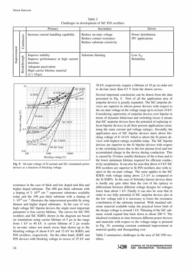
Introduction of SiC power devices will change with timethe scene of preferred semiconductor devices used in dif-ferent applications. It is important for the system designerand semiconductor device engineer alike to be able to un-derstand the potential and limitations of different devicesas well predict the pace of their development. In Fig. 9the ideal performance limits of unipolar and bipolar Si andSiC power devices are shown in the domain of on-statevoltage and blocking voltage. In the Si case the on-statevoltage curves based on the actual device data are shownfor fast PiN rectifiers, MOSFETs, IGBTs and GTO thyris-tors together with an ideal limit equal to the resistivity ofthe uniformly doped drift region of unipolar device only.In the SiC case the on-state voltage curves based on devicesimulations are shown for DMOS and UMOS transistors,vertical JFETs, Schottky barrier rectifiers, PiN rectifiers andIGBTs. The SiC device data represent the ideal limit fordifferent types of devices. The device lateral design useshigh-density layout with small cell pitch equal to 3 µm,5 µm and 10 µm for UMOSFET, VJFET and DMOSFET,respectively. The ideal bulk mobility is assumed for allthe devices in both the channel and the drift region. Thecontribution from substrate resistance is included and min-imised assuming only 100 µm thick substrate with a dopingof 1 ·1019 cm−3. The ideal limit for 4H-SiC based on theresistivity of the uniformly doped unipolar device drift re-gion only is shown including the influence of the substrate
J O U R N AL O F T E L E CO M M U N I CAT I O N SAN D I N FO R M AT I O N T E C H N O LO GY 3-4/2000 23
Mietek Bakowski
Table 2Challenges in development of SiC PiN rectifiers
Primary Secondary Driver
Impr
ovem
ent
Con
tinuo
us Increase current handling capability Reduce on-state voltageReduce contact resistanceReduce substrate resistivity
Power distributionHV applications
Bre
akth
roug
h Improve stabilityImprove performance at high currentdensitiesAdequate passivationHigh carrier lifetime material(2÷10 µs)
Substrate thinning Low Von
Reliability
Fig. 9. On-state voltage of Si (actual) and SiC (simulated) powerdevices as a function of blocking voltage.
resistance in the case of thick and low doped and thin andhigher doped substrate. The 400 µm thick substrate witha doping of 5 · 1018 cm−3 represents substrates availabletoday and the 100 µm thick substrate with a doping of1 ·1019 cm−3 illustrates the improvement possible by usingthinner and higher doped substrates. In the case of veryhigh voltage SiC bipolar devices the single most importantparameter is free carrier lifetime. The curves for SiC PiNrectifiers and SiC IGBTs shown in the diagram are basedon simulations using carrier lifetime of 5 µs in the rangefrom 1 kV to 40 kV. A carrier lifetime of 2 µs resultsin on-state values not much worse than shown up to theblocking voltage of about 6 kV and 15 kV for IGBTs andPiN rectifiers, respectively. On the other hand, IGBT andPiN devices with blocking voltage in excess of 25 kV and
30 kV, respectively, require a lifetime of 10 µs in order notto deviate more than 0.5 V from the drawn curves.
Several important conclusions can be drawn from the datapresented in Fig. 9. First of all the application area ofunipolar devices is greatly expanded. The SiC unipolar de-vices are superior to silicon power devices with respect tothe on-state voltage in the voltage range up to at least 10 kV.Considering superiority of unipolar devices over bipolar interms of dynamic behaviour and switching losses it meansthat SiC unipolar devices have the potential of replacing si-licon bipolar devices in all their present applications (assu-ming the same current and voltage ratings). Secondly, theapplication area of SiC bipolar devices starts above blo-cking voltage of 8–10 kV which is above the Si power de-vices with highest ratings available today. The SiC bipolardevices are superior to the Si bipolar devices with respectto the switching losses due to the low plasma level and lowaccumulated charge in the device during conduction. Thisis caused by 10 times smaller thickness of the n-base and tothe lower minimum lifetime required for efficient conduc-tivity modulation. It can also be seen that above 4.5 kV SiCPiN rectifiers are superior to Si PiN rectifiers also with re-spect to the on-state voltage. The same applies to the SiCIGBTs with voltage rating above 2.5 kV as compared tothe Si IGBTs. In the case of Schottky barrier devices thereis hardly any gain other than the cost of the epitaxy todifferentiate between different voltage designs for voltageslower than about 1 kV. Finally it can also be seen that inorder to use fully potential of SiC unipolar devices also atthe low voltage end it is necessary to lower the resistancecontribution of the substrate material. With standard sub-strate material available today the practical lower limit ofthe design voltage is around 1 kV. Thinning of the SiC sub-strate would expand that limit down to about 200 V. Theidealised evolution in time between different power devicesand materials with respect to the voltage range is picturedin Fig. 10; assuming constant continued improvement inmaterial quality and disregarding cost.
Table 2 summarises challenges in the area of SiC PiN rec-tifiers.
24J O U R N AL O F T E L E CO M M U N I CAT I O N SAN D I N FO R M AT I O N T E C H N O LO GY3-4/2000
Roadmap for SiC power devices
Fig. 10. Preferred device type and semiconductor material basedon the data in Fig. 9.
5.2. Unipolar devices
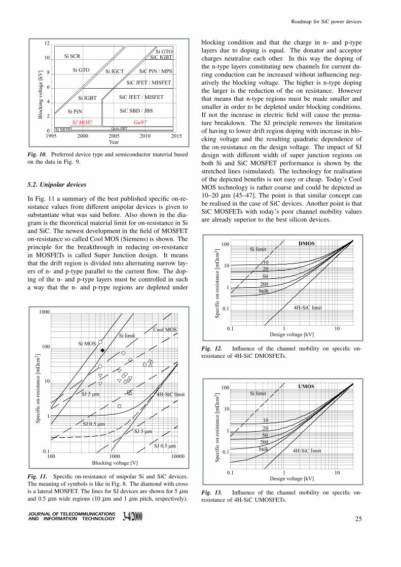
In Fig. 11 a summary of the best published specific on-re-sistance values from different unipolar devices is given tosubstantiate what was said before. Also shown in the dia-gram is the theoretical material limit for on-resistance in Siand SiC. The newest development in the field of MOSFETon-resistance so called Cool MOS (Siemens) is shown. Theprinciple for the breakthrough in reducing on-resistancein MOSFETs is called Super Junction design. It meansthat the drift region is divided into alternating narrow lay-ers of n- and p-type parallel to the current flow. The dop-ing of the n- and p-type layers must be controlled in sucha way that the n- and p-type regions are depleted under
Fig. 11. Specific on-resistance of unipolar Si and SiC devices.The meaning of symbols is like in Fig. 8. The diamond with crossis a lateral MOSFET. The lines for SJ devices are shown for 5 µmand 0.5 µm wide regions (10 µm and 1 µm pitch, respectively).
blocking condition and that the charge in n- and p-typelayers due to doping is equal. The donator and acceptorcharges neutralise each other. In this way the doping ofthe n-type layers constituting new channels for current du-ring conduction can be increased without influencing neg-atively the blocking voltage. The higher is n-type dopingthe larger is the reduction of the on resistance. Howeverthat means that n-type regions must be made smaller andsmaller in order to be depleted under blocking conditions.If not the increase in electric field will cause the prema-ture breakdown. The SJ principle removes the limitationof having to lower drift region doping with increase in blo-cking voltage and the resulting quadratic dependence ofthe on-resistance on the design voltage. The impact of SJdesign with different width of super junction regions onboth Si and SiC MOSFET performance is shown by thestretched lines (simulated). The technology for realisationof the depicted benefits is not easy or cheap. Today’s CoolMOS technology is rather coarse and could be depicted as10–20 µm [45–47]. The point is that similar concept canbe realised in the case of SiC devices. Another point is thatSiC MOSFETs with today’s poor channel mobility valuesare already superior to the best silicon devices.
Fig. 12. Influence of the channel mobility on specific on-resistance of 4H-SiC DMOSFETs.
Fig. 13. Influence of the channel mobility on specific on-resistance of 4H-SiC UMOSFETs.
J O U R N AL O F T E L E CO M M U N I CAT I O N SAN D I N FO R M AT I O N T E C H N O LO GY 3-4/2000 25
Mietek Bakowski
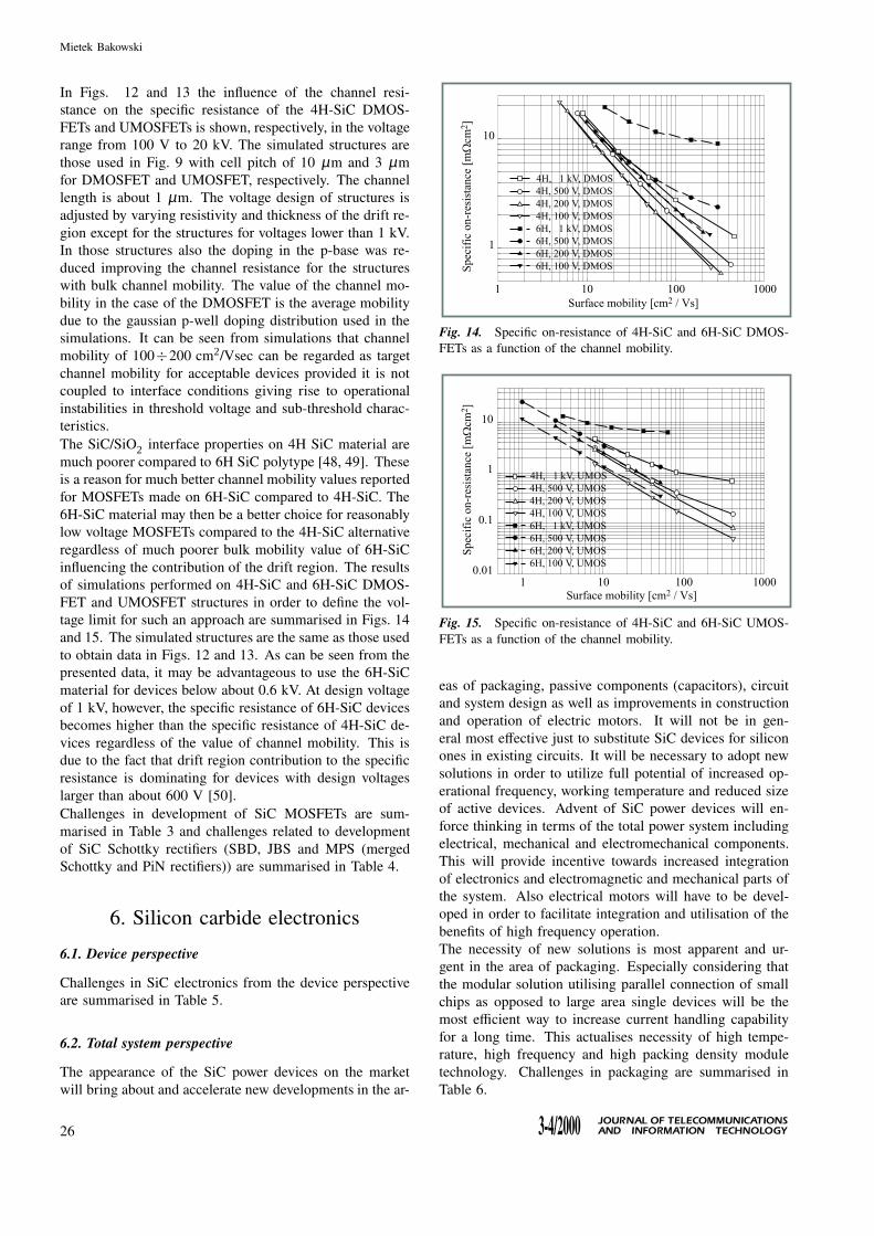
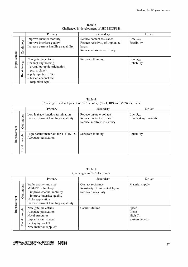
In Figs. 12 and 13 the influence of the channel resi-stance on the specific resistance of the 4H-SiC DMOS-FETs and UMOSFETs is shown, respectively, in the voltagerange from 100 V to 20 kV. The simulated structures arethose used in Fig. 9 with cell pitch of 10 µm and 3 µmfor DMOSFET and UMOSFET, respectively. The channellength is about 1 µm. The voltage design of structures isadjusted by varying resistivity and thickness of the drift re-gion except for the structures for voltages lower than 1 kV.In those structures also the doping in the p-base was re-duced improving the channel resistance for the structureswith bulk channel mobility. The value of the channel mo-bility in the case of the DMOSFET is the average mobilitydue to the gaussian p-well doping distribution used in thesimulations. It can be seen from simulations that channelmobility of 100÷200 cm2/Vsec can be regarded as targetchannel mobility for acceptable devices provided it is notcoupled to interface conditions giving rise to operationalinstabilities in threshold voltage and sub-threshold charac-teristics.The SiC/SiO2 interface properties on 4H SiC material aremuch poorer compared to 6H SiC polytype [48, 49]. Theseis a reason for much better channel mobility values reportedfor MOSFETs made on 6H-SiC compared to 4H-SiC. The6H-SiC material may then be a better choice for reasonablylow voltage MOSFETs compared to the 4H-SiC alternativeregardless of much poorer bulk mobility value of 6H-SiCinfluencing the contribution of the drift region. The resultsof simulations performed on 4H-SiC and 6H-SiC DMOS-FET and UMOSFET structures in order to define the vol-tage limit for such an approach are summarised in Figs. 14and 15. The simulated structures are the same as those usedto obtain data in Figs. 12 and 13. As can be seen from thepresented data, it may be advantageous to use the 6H-SiCmaterial for devices below about 0.6 kV. At design voltageof 1 kV, however, the specific resistance of 6H-SiC devicesbecomes higher than the specific resistance of 4H-SiC de-vices regardless of the value of channel mobility. This isdue to the fact that drift region contribution to the specificresistance is dominating for devices with design voltageslarger than about 600 V [50].Challenges in development of SiC MOSFETs are sum-marised in Table 3 and challenges related to developmentof SiC Schottky rectifiers (SBD, JBS and MPS (mergedSchottky and PiN rectifiers)) are summarised in Table 4.
6. Silicon carbide electronics
6.1. Device perspective
Challenges in SiC electronics from the device perspectiveare summarised in Table 5.
6.2. Total system perspective
The appearance of the SiC power devices on the marketwill bring about and accelerate new developments in the ar-
Fig. 14. Specific on-resistance of 4H-SiC and 6H-SiC DMOS-FETs as a function of the channel mobility.
Fig. 15. Specific on-resistance of 4H-SiC and 6H-SiC UMOS-FETs as a function of the channel mobility.
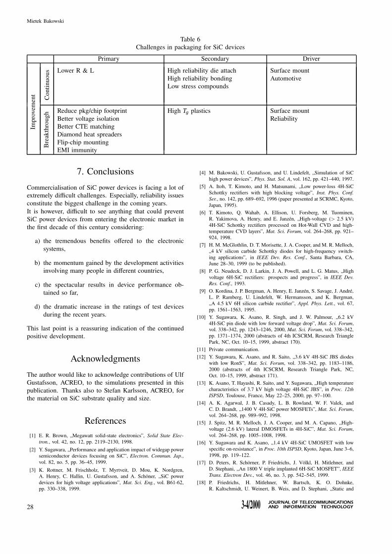
eas of packaging, passive components (capacitors), circuitand system design as well as improvements in constructionand operation of electric motors. It will not be in gen-eral most effective just to substitute SiC devices for siliconones in existing circuits. It will be necessary to adopt newsolutions in order to utilize full potential of increased op-erational frequency, working temperature and reduced sizeof active devices. Advent of SiC power devices will en-force thinking in terms of the total power system includingelectrical, mechanical and electromechanical components.This will provide incentive towards increased integrationof electronics and electromagnetic and mechanical parts ofthe system. Also electrical motors will have to be devel-oped in order to facilitate integration and utilisation of thebenefits of high frequency operation.The necessity of new solutions is most apparent and ur-gent in the area of packaging. Especially considering thatthe modular solution utilising parallel connection of smallchips as opposed to large area single devices will be themost efficient way to increase current handling capabilityfor a long time. This actualises necessity of high tempe-rature, high frequency and high packing density moduletechnology. Challenges in packaging are summarised inTable 6.
26J O U R N AL O F T E L E CO M M U N I CAT I O N SAN D I N FO R M AT I O N T E C H N O LO GY3-4/2000
Roadmap for SiC power devices
Table 3Challenges in development of SiC MOSFETs
Primary Secondary Driver
Impr
ovem
ent
Con
tinuo
us
Improve channel mobilityImprove interface qualityIncrease current handling capability
Reduce contact resistanceReduce resistivity of implantedlayersReduce substrate resistivity
Low Ron
Feasibility
Bre
akth
roug
h New gate dielectricsChannel engineering– crystallographic orientation
(ex. a-plane)– polytype (ex. 15R)– buried channel etc.
(depletion type)
Substrate thinning Low Ron
Reliability
Table 4Challenges in development of SiC Schottky (SBD, JBS and MPS) rectifiers
Primary Secondary Driver
Impr
ovem
ent
Con
tinuo
us Low leakage junction terminationIncrease current handling capability
Reduce on-state voltageReduce contact resistanceReduce substrate resistivity
Low Ron
Low leakage currents
Bre
akth
roug
h High barrier materials for T > 150◦ CAdequate passivation
Substrate thinning Reliability
Table 5Challenges in SiC electronics
Primary Secondary Driver
Impr
ovem
ent
Con
tinuo
us Wafer quality and sizeMISFET technology– improve channel mobility– improve interface qualityNiche applicationIncrease current handling capability
Contact resistanceResistivity of implanted layersSubstrate resistivity
Material supply
Bre
akth
roug
h New gate dielectricsAdequate passivationNovel structuresImplantation damagePackaging for HTNew material suppliers
Carrier lifetime SpeedLossesHigh TjSystem benefits
J O U R N AL O F T E L E CO M M U N I CAT I O N SAN D I N FO R M AT I O N T E C H N O LO GY 3-4/2000 27
Mietek Bakowski
Table 6Challenges in packaging for SiC devices
Primary Secondary Driver
Impr
ovem
ent
Con
tinuo
us Lower R & L High reliability die attachHigh reliability bondingLow stress compounds
Surface mountAutomotive
Bre
akth
roug
h Reduce pkg/chip footprintBetter voltage isolationBetter CTE matchingDiamond heat spreadersFlip-chip mountingEMI immunity
High Tg plastics Surface mountReliability
7. Conclusions
Commercialisation of SiC power devices is facing a lot ofextremely difficult challenges. Especially, reliability issuesconstitute the biggest challenge in the coming years.It is however, difficult to see anything that could preventSiC power devices from entering the electronic market inthe first decade of this century considering:
a) the tremendous benefits offered to the electronicsystems,
b) the momentum gained by the development activitiesinvolving many people in different countries,
c) the spectacular results in device performance ob-tained so far,
d) the dramatic increase in the ratings of test devicesduring the recent years.
This last point is a reassuring indication of the continuedpositive development.
Acknowledgments
The author would like to acknowledge contributions of UlfGustafsson, ACREO, to the simulations presented in thispublication. Thanks also to Stefan Karlsson, ACREO, forthe material on SiC substrate quality and size.
References
[1] E. R. Brown, „Megawatt solid-state electronics”, Solid State Elec-tron., vol. 42, no. 12, pp. 2119–2130, 1998.
[2] Y. Sugawara, „Performance and application impact of widegap powersemiconductor devices focusing on SiC”, Electron. Commun. Jap.,vol. 82, no. 5, pp. 36–45, 1999.
[3] K. Rottner, M. Frischholz, T. Myrtveit, D. Mou, K. Nordgren,A. Henry, C. Hallin, U. Gustafsson, and A. Schoner, „SiC powerdevices for high voltage applications”, Mat. Sci. Eng., vol. B61-62,pp. 330–338, 1999.
[4] M. Bakowski, U. Gustafsson, and U. Lindefelt, „Simulation of SiChigh power devices”, Phys. Stat. Sol. A, vol. 162, pp. 421–440, 1997.
[5] A. Itoh, T. Kimoto, and H. Matsunami, „Low power-loss 4H-SiCSchottky rectifiers with high blocking voltage”, Inst. Phys. Conf.Ser., no. 142, pp. 689–692, 1996 (paper presented at SCRMC, Kyoto,Japan, 1995).
[6] T. Kimoto, Q. Wahab, A. Ellison, U. Forsberg, M. Tuominen,R. Yakimova, A. Henry, and E. Janzen, „High-voltage (> 2.5 kV)4H-SiC Schottky rectifiers processed on Hot-Wall CVD and high-temperature CVD layers”, Mat. Sci. Forum, vol. 264–268, pp. 921–924, 1998.
[7] H. M. McGlothlin, D. T. Morisette, J. A. Cooper, and M. R. Melloch,„4 kV silicon carbide Schottky diodes for high-frequency switch-ing applications”, in IEEE Dev. Res. Conf., Santa Barbara, CA,June 28–30, 1999 (to be published).
[8] P. G. Neudeck, D. J. Larkin, J. A. Powell, and L. G. Matus, „Highvoltage 6H-SiC rectifiers: prospects and progress”, in IEEE Dev.Res. Conf., 1993.
[9] O. Kordina, J. P. Bergman, A. Henry, E. Janzen, S. Savage, J. Andre,L. P. Ramberg, U. Lindefelt, W. Hermansson, and K. Bergman,„A 4.5 kV 6H silicon carbide rectifier”, Appl. Phys. Lett., vol. 67,pp. 1561–1563, 1995.
[10] Y. Sugawara, K. Asano, R. Singh, and J. W. Palmour, „6.2 kV4H-SiC pin diode with low forward voltage drop”, Mat. Sci. Forum,vol. 338–342, pp. 1243–1246, 2000, Mat. Sci. Forum, vol. 338–342,pp. 1371–1374, 2000 (abstracts of 4th ICSCRM, Research TrianglePark, NC, Oct. 10–15, 1999, abstract 170).
[11] Private communication.[12] Y. Sugawara, K. Asano, and R. Saito, „3.6 kV 4H-SiC JBS diodes
with low RonS”, Mat. Sci. Forum, vol. 338–342, pp. 1183–1186,2000 (abstracts of 4th ICSCRM, Research Triangle Park, NC,Oct. 10–15, 1999, abstract 171).
[13] K. Asano, T. Hayashi, R. Saito, and Y. Sugawara, „High temperaturecharacteristics of 3.7 kV high voltage 4H-SiC JBS”, in Proc. 12thISPSD, Toulouse, France, May 22–25, 2000, pp. 97–100.
[14] A. K. Agarwal, J. B. Casady, L. B. Rowland, W. F. Valek, andC. D. Brandt, „1400 V 4H-SiC power MOSFETs”, Mat. Sci. Forum,vol. 264–268, pp. 989–992, 1998.
[15] J. Spitz, M. R. Melloch, J. A. Cooper, and M. A. Capano, „High-voltage (2.6 kV) lateral DMOSFETs in 4H-SiC”, Mat. Sci. Forum,vol. 264–268, pp. 1005–1008, 1998.
[16] Y. Sugawara and K. Asano, „1.4 kV 4H-SiC UMOSFET with lowspecific on-resistance”, in Proc. 10th ISPSD, Kyoto, Japan, June 3–6,1998, pp. 119–122.
[17] D. Peters, R. Schorner, P. Friedrichs, J. Volkl, H. Mitlehner, andD. Stephani, „An 1800 V triple implanted 6H-SiC MOSFET”, IEEETrans. Electron Dev., vol. 46, no. 3, pp. 542–545, 1999.
[18] P. Friedrichs, H. Mitlehner, W. Bartsch, K. O. Dohnke,R. Kaltschmidt, U. Weinert, B. Weis, and D. Stephani, „Static and
28J O U R N AL O F T E L E CO M M U N I CAT I O N SAN D I N FO R M AT I O N T E C H N O LO GY3-4/2000
Roadmap for SiC power devices
dynamic characteristics of 4H-SiC JFETs designed for different blo-cking categories”, Mat. Sci. Forum, vol. 338–342, pp. 1243–1246,2000 (abstracts of 4th ICSCRM, Research Triangle Park, NC, Oct.10–15, 1999, abstract 75, to be published).
[19] P. Friedrichs, H. Mitlehner, K. O. Dohnke, D. Peters, R. Schorner,U. Weinert, E. Baudelot, and D. Stephani, „SiC power devices withlow on-resistance for fast switching applications”, in Proc. 12thISPSD, Toulouse, France, May 22–25, 2000, pp. 213–216.
[20] Y. Sugawara, K. Asano, R. Singh, J. Palmour, and D. Takayama,„4.5 kV novel high voltage high performance SiC-FET SIAFET”,in Proc. 12th ISPSD, Toulouse, France, May 22–25, 2000, pp. 105–108.
[21] J. B. Casady, A. K. Agarwal, L. B. Rowland, R. R. Siergiej,S. Seshadri, S. Mani, J. Barrows, D. Piccone, P. A. Sanger, andC. D. Brandt, „4H-SiC gate turn-off (GTO) thyristor development”,Mat. Sci. Forum, vol. 264–268, pp. 1069–1072, 1998.
[22] A. Agarwal, S.-H. Ryu, R. Singh, and J. Palmour, „2600 V, 12 A,4H-SiC, asymmetrical gate turn-off (GTO) thyristor development”,Mat. Sci. Forum, vol. 338–342, pp. 1387–1390, 2000 (abstracts of4th ICSCRM, Research Triangle Park, NC, Oct. 10–15, 1999, ab-stract 474).
[23] H. Lendenmann, N. Johansson, D. Mou, M. Frischholz, B. Astrand,P. Isberg, and C. Ovren, „Operation of a 2500 V 150 A Si-IGBT/SiCdiode module”, Mat. Sci. Forum, vol. 338–342, pp. 1423–1426, 2000(abstracts of 4th ICSCRM, Research Triangle Park, NC, Oct. 10–15,1999, abstract 189).
[24] C. H. Carter, V. F. Tsvedkov, R. C. Glass, D. Henshall, M. Brady,St. G. Muller, O. Kordina, K. Irvine, J. A. Edmond, H. S. Kong,R. Singh, S. T. Allen, and J. W. Palmour, „Progress in SiC: frommaterial growth to commercial device development”, Mat. Sci. Eng.,vol. B61-61, pp. 1–8, 1999.
[25] G. M. Dolny, D. T. Morisette, P. M. Shenoy, M. Zafrani, J. Gla-dish, J. M. Woodall, J. A. Cooper, and M. R. Melloch, „Staticand dynamic characterisation of large-area high-current-density SiCSchottky diodes”, in IEEE Dev. Res. Conf., Charlottesville, VA,June 22–24, 1998.
[26] R. Rupp, M. Treu, A. Mauder, E. Griebl, W. Werner, W. Bartsch,and D. Stephani, „Performance and reliability issues of SiC-Schottkydiodes”, Mat. Sci. Forum, vol. 338–342, pp. 1167–1170, 2000 (ab-stracts of 4th ICSCRM, Research Triangle Park, NC, Oct. 10–15,1999, abstract 37).
[27] R. Held, M. Fullmann, and E. Niemann, „SiC-power rectifiers”,Mat. Sci. Forum, vol. 338–342, pp. 1407–1410, 2000 (abstracts of4th ICSCRM, Research Triangle Park, NC, Oct. 10–15, 1999, ab-stract 7).
[28] P. G. Neudeck, J. B. Petit, and C. S. Salupo, „Silicon carbide buried-gate junction field effect transistors for high-temperature power elec-tronic applications”, in Second Int. High Temp. Electron. Conf., Char-lotte, NC, June 6–10, 1994.
[29] A. O. Konstantinov and H. Bleichner, „Bright-line defect formationin silicon carbide injection diodes”, Appl. Phys. Lett., vol. 71 (25),pp. 3700–3702, 1997.
[30] J. A. Powell and D. J. Larkin, „Process-induced morphological de-fects in epitaxial CVD silicon carbide”, Phys. Stat. Sol. B, vol. 202,pp. 529–548, 1997.
[31] U. Zimmerman, A. Hallen, A. O. Konstantinov, and B. Breitholz,„Investigations of microplasma breakdown in 4H silicon carbide”,in Mat. Res. Soc. Symp. Proc., vol. 512, pp. 512–516, 1998.
[32] M. Frischholtz, J. Seidel, A. Schoner, U. Gustafsson, M. Bakowski,K. Nordgren, and K. Rottner, „JTE concept evaluation and failureanalysis: OBIC measurements on 4H SiC p+-n diodes”, in Proc.10th ISPSD, Kyoto, Japan, June 3–6, 1998, pp. 391–394.
[33] N. Keskar, K. Shenai, and P. Neudeck, „Characterisation and mod-eling of SiC p-n diode”, Mat. Sci. Forum, vol. 338–342, pp. 1351–1354, 2000 (abstracts of 4th ICSCRM, Research Triangle Park, NC,Oct. 10–15, 1999, abstract 190).
[34] A. Galeckas, J. Linnros, and B. Breitholtz, „Optical characterisationof 4H-SiC p+n−n+ structures applying time- and spectrally resol-ved emission microscopy”, Mat. Sci. Forum, vol. 338–342, pp. 683–686, 2000 (abstracts of 4th ICSCRM, Research Triangle Park, NC,Oct. 10–15, 1999, abstract 196).
[35] N. Ramungul and T. P. Chow, „Current-controlled negative resistance(CCNR) in SiC PiN rectifiers”, IEEE Trans. Electron Dev., vol. 46,no. 3, pp. 493–496, 1999.
[36] T. Kimoto, N. Miyamoto, and H. Matsunami, „Performance limitingsurface defects in SiC epitaxial p-n junction diodes”, IEEE Trans.Electron Dev., vol. 46, no. 3, pp. 471–477, 1999.
[37] P. G. Neudeck, W. Huang, and M. Dudley, „Study of bulk and ele-mentary screw dislocation assisted reverse breakdown in low-voltage(< 250 V) 4H-SiC p+n junction diodes. Part I: DC properties”, IEEETrans. Electron Dev., vol. 46, no. 3, pp. 478–484, 1999.
[38] P. G. Neudeck and C. Fazi, „Study of bulk and elementary screwdislocation assisted reverse breakdown in low-voltage (< 250 V) 4H-SiC p+n junction diodes. Part II: Dynamic breakdown properties”,IEEE Trans. Electron Dev., vol. 46, no. 3, pp. 485–492, 1999.
[39] L. A. Lipkin and J. P. Palmour, „Insulator investigation on SiC forimproved reliability”, IEEE Trans. Electron Dev., vol. 46, no. 3,pp. 525–532, 1999.
[40] S. Sridevan, P. K. McLarty, and B. J. Baliga, „Analysis of gatedielectrics for SiC power UMOSFETs”, in Proc. 9th ISPSD, Weimar,Germany, May 26–29, 1997, pp. 153–156.
[41] L. A. Lipkin and J. P. Palmour, „SiC devices with ONO stackeddielectrics”, Mat. Sci. Forum, vol. 338–342, pp. 1093–1096, 2000(abstracts of 4th ICSCRM, Research Triangle Park, NC, Oct. 10–15,1999, abstract 348).
[42] W. J. Zhu, X. W. Wang, and T. P. Ma, „Highly durable SiC nMES-FET at 450◦C”, Mat. Sci. Forum, vol. 338–342, pp. 1311–1314, 2000(abstracts of 4th ICSCRM, Research Triangle Park, NC, Oct. 10–15,1999, abstract 464).
[43] C. I. Harris, M. O. Aboelfotoh, R. S. Kern, S. Tanaka, andR. F. Davis, „Low interface state densities in SiC MIS devices usingepitaxial AlN”, Inst. Phys. Conf. Ser., vol. 142, pp. 777–780, 1995.
[44] C. M. Zetterling, M. Ostling, H. Yano, T. Kimoto, H. Matsunami,K. Linthicum, and R. F. Davis, „SiC MISFETs with MBE grownAlN gate dielectric”, Mat. Sci. Forum, vol. 338–342, pp. 1315–1318, 2000 (abstracts of 4th ICSCRM, Research Triangle Park, NC,Oct. 10–15, 1999, abstract 203).
[45] G. Deboy, M. Marz, J.-P. Stengl, H. Sack, J. Tihanyi, and H. Weber,„A new generation of high voltage MOSFETs breaks the limit lineof silicon”, in Proc. IEDM, San Francisco, CA, Dec. 6–9, 1998,pp. 683–685.
[46] L. Lorenz, G. Deboy, M. Marz, J.-P. Stengl, and A. Bachofner,„Drastic reduction of on-resistance with COOLMOS”, PCIM Eur.,vol. 5, pp. 250–258, 1998.
[47] L. Lorenz, G. Deboy, A. Knapp, and M. Marz, „COOLMOSTM –a new milestone in high voltage power MOS”, in Proc. 11th ISPSD,Toronto, Ontario, Canada, May 25–28, 1999, pp. 3–10.
[48] R. Schorner, P. Friedrichs, D. Peters, and D. Stephani, „Significantlyimproved performance of MOSFET’s on silicon carbide using the15R-SiC polytype”, IEEE Electron Dev. Lett., vol. 20, no. 5, pp. 241–244, 1999.
[49] M. Bassler, V. Afanasjev, and G. Pensl, „Electrically active traps atthe 4H-SiC/SiO2 interface responsible for the limitation of the chan-nel mobility”, Mat. Sci. Forum, vol. 338–342, pp. 1065–1068, 2000(abstracts of 4th ICSCRM, Research Triangle Park, NC, Oct. 10–15,1999, abstract 239).
[50] M. Bakowski and U. Gustafsson, „Optimisation and comparison oflosses in Si and 4H SiC 1 kV trench MOSFETs”, in Proc. 26th Eur.Solid State Dev. Res. Conf., 1996, pp. 583–586 (editions frontieres).
Mietek Bakowski received the Ph.D. degree and theAssistant Professor competence from Chalmers Universityof Technology, Gothenburg, in 1974 and 1981, respectively.In 1975/76 and 1977/78 he visited Jet Propulsion Labo-ratory, Pasadena, CA, studying oxide reliability in MOSdevices. In 1983 he joined ABB, Vdsteras, leading GTO
J O U R N AL O F T E L E CO M M U N I CAT I O N SAN D I N FO R M AT I O N T E C H N O LO GY 3-4/2000 29

Mietek Bakowski
development projects. In 1991 he joined Institute of Mi-croelectronics, Kista, working with development and eval-uation of silicon power devices. Since 1994 he is withSiC Electronics group at (IMC) ACREO, Kista, workingwith the design, simulation and electrical evaluation of SiCdevices. He is a part-time Professor at Royal Institute ofTechnology, Kista.e-mail: [email protected] ABElectrum 236, SE-164 40Kista, Sweden
30J O U R N AL O F T E L E CO M M U N I CAT I O N SAN D I N FO R M AT I O N T E C H N O LO GY3-4/2000


![Chapter 2 SiC Materials and Processing Technology€¦ · 34 2 SiC Materials and Processing Technology Table 2.1 Key electrical parameters of SiC [1] Property 4H-SiC 6H-SiC 3C-SiC](https://img.pdfslide.us/doc/110x75/5f4fd11797ddad63bf719816/chapter-2-sic-materials-and-processing-technology-34-2-sic-materials-and-processing.jpg)