Embed Size (px)
Citation preview
RN4677Bluetooth® 4.0 Dual Mode Module
Features
• Complete, fully certified, embedded 2.4 GHz Bluetooth® version 4.0 module
• Bluetooth Classic (BR/EDR) and Low Energy (LE)
• Bluetooth SIG certified
• On-board embedded Bluetooth stack
• Transparent UART mode for seamless serial data over Bluetooth Classic uses Serial Port Profile (SPP), and Bluetooth Low Energy uses Generic Attribute (GATT) Profile.
• Capability to open data connection in both Bluetooth Classic (Master) and Low Energy (Central) roles
• Easy to configure with ASCII commands, PC UI utility, or PIC® MCU driver library
• Firmware is upgradeable via UART
• Compact surface mount module: 22 x 12 x 2.4 mm
• Castellated surface mount pads for easy and reliable host PCB mounting
• Environmentally friendly, RoHS compliant
• Perfect for Portable Battery-Operated Devices
• Internal Battery Regulator Circuitry
• Worldwide regulatory certifications
Operational
• Single operating voltage: 3.2V to 4.3V
• Temperature range: -20°C to 70°C
• Simple, UART interface
• Integrated Crystal, Internal Voltage Regulator, and Matching Circuitry
• Multiple I/O pins for control and status
RF/Analog
• Frequency: 2.402 to 2.480 GHz
• Receive Sensitivity: -90 dBm (Classic); -92 dBm (LE)
• Power Output: 2 dBm (typical)
Data Throughput
• 50 kilobytes (Classic on Android)
• 8 kilobytes (LE on iOS7)
MAC/Baseband/Higher Layer
• Secure AES128 encryption
• GAP, SDP, SPP, and GATT profiles
Antenna• Ceramic Chip Antenna (RN4677)
• External Antenna Connection via RF Pad (RN4677U)
Compliance
• Bluetooth SIG QDID: B021961
• Modular Certified for the United States (FCC) and Canada (IC)
• European R&TTE Directive Assessed Radio Module
General Description
The RN4677 is a fully certified Bluetooth version 4.0(BR/EDR/LE) module, which enables the designers toeasily add dual mode Bluetooth wireless capability totheir products. Delivering local connectivity for theInternet of Things (IoT), the RN4677 bridges theproduct to Smart Phones and Tablets for convenientdata transfer, control and access to cloud applications.
This Bluetooth SIG certified module provides acomplete wireless solution with Bluetooth stack on-board, integrated antenna, and worldwide radiocertifications in a compact surface mount package, 22 x 12 x 2.4 mm. It supports GAP, SDP, SPP, andGATT profiles. Data is transferred over the Bluetoothlink by sending/receiving data via transparent UARTmode, making it easy to integrate with any processor orMicrocontroller with a UART interface. Configuration ismade easy using a ASCII commands via UART.Windows® based GUI, or PIC MCU configuration driverare also used to access configuration settings overUART.
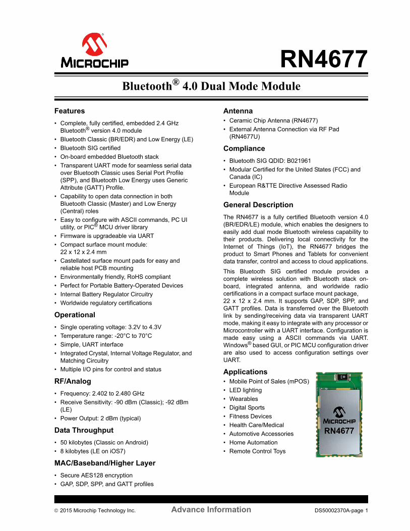
Applications• Mobile Point of Sales (mPOS)
• LED lighting
• Wearables
• Digital Sports
• Fitness Devices
• Health Care/Medical
• Automotive Accessories
• Home Automation
• Remote Control Toys
2015 Microchip Technology Inc. Advance Information DS50002370A-page 1
RN4677
Table of Contents
1.0 Device Overview .......................................................................................................................................................................... 32.0 Application Information................................................................................................................................................................113.0 Regulatory Approval ................................................................................................................................................................... 134.0 Electrical Characteristics ............................................................................................................................................................ 175.0 Ordering Information .................................................................................................................................................................. 19Appendix A: Revision History............................................................................................................................................................... 21The Microchip Web Site ....................................................................................................................................................................... 23Customer Change Notification Service ................................................................................................................................................ 23Customer Support ................................................................................................................................................................................ 23Product Identification System............................................................................................................................................................... 25
TO OUR VALUED CUSTOMERS
It is our intention to provide our valued customers with the best documentation possible to ensure successful use of your Microchipproducts. To this end, we will continue to improve our publications to better suit your needs. Our publications will be refined andenhanced as new volumes and updates are introduced.
If you have any questions or comments regarding this publication, please contact the Marketing Communications Department viaE-mail at [email protected]. We welcome your feedback.
Most Current Data Sheet
To obtain the most up-to-date version of this data sheet, please register at our Worldwide Web site at:
http://www.microchip.com
You can determine the version of a data sheet by examining its literature number found on the bottom outside corner of any page.The last character of the literature number is the version number, (e.g., DS30000000A is version A of document DS30000000).
Errata
An errata sheet, describing minor operational differences from the data sheet and recommended workarounds, may exist for currentdevices. As device/documentation issues become known to us, we will publish an errata sheet. The errata will specify the revisionof silicon and revision of document to which it applies.
To determine if an errata sheet exists for a particular device, please check with one of the following:
• Microchip’s Worldwide Web site; http://www.microchip.com• Your local Microchip sales office (see last page)When contacting a sales office, please specify which device, revision of silicon and data sheet (include literature number) you areusing.
Customer Notification System
Register on our web site at www.microchip.com to receive the most current information on all of our products.
DS50002370A-page 2 Advance Information 2015 Microchip Technology Inc.
RN4677
1.0 DEVICE OVERVIEW
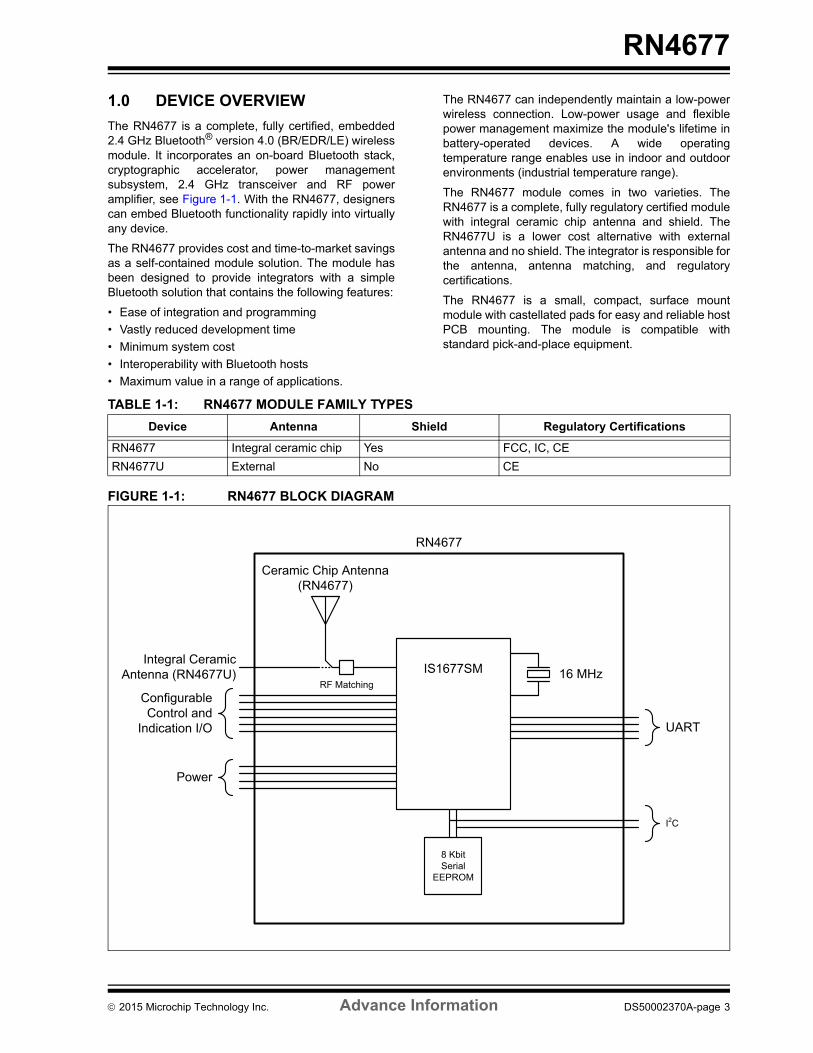
The RN4677 is a complete, fully certified, embedded2.4 GHz Bluetooth® version 4.0 (BR/EDR/LE) wirelessmodule. It incorporates an on-board Bluetooth stack,cryptographic accelerator, power managementsubsystem, 2.4 GHz transceiver and RF poweramplifier, see Figure 1-1. With the RN4677, designerscan embed Bluetooth functionality rapidly into virtuallyany device.
The RN4677 provides cost and time-to-market savingsas a self-contained module solution. The module hasbeen designed to provide integrators with a simpleBluetooth solution that contains the following features:
• Ease of integration and programming
• Vastly reduced development time
• Minimum system cost
• Interoperability with Bluetooth hosts
• Maximum value in a range of applications.
The RN4677 can independently maintain a low-powerwireless connection. Low-power usage and flexiblepower management maximize the module's lifetime inbattery-operated devices. A wide operatingtemperature range enables use in indoor and outdoorenvironments (industrial temperature range).
The RN4677 module comes in two varieties. TheRN4677 is a complete, fully regulatory certified modulewith integral ceramic chip antenna and shield. TheRN4677U is a lower cost alternative with externalantenna and no shield. The integrator is responsible forthe antenna, antenna matching, and regulatorycertifications.
The RN4677 is a small, compact, surface mountmodule with castellated pads for easy and reliable hostPCB mounting. The module is compatible withstandard pick-and-place equipment.
FIGURE 1-1: RN4677 BLOCK DIAGRAM
TABLE 1-1: RN4677 MODULE FAMILY TYPES
Device Antenna Shield Regulatory Certifications
RN4677 Integral ceramic chip Yes FCC, IC, CE
RN4677U External No CE
Ceramic Chip Antenna(RN4677)
RF MatchingConfigurableControl andIndication I/O UART
16 MHzIntegral Ceramic
Antenna (RN4677U)
I2C
8 KbitSerial
EEPROM
IS1677SM
Power
RN4677
2015 Microchip Technology Inc. Advance Information DS50002370A-page 3
RN4677
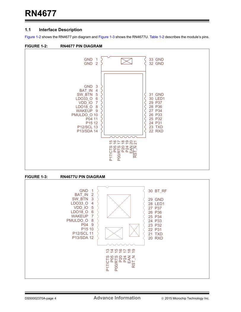
1.1 Interface Description
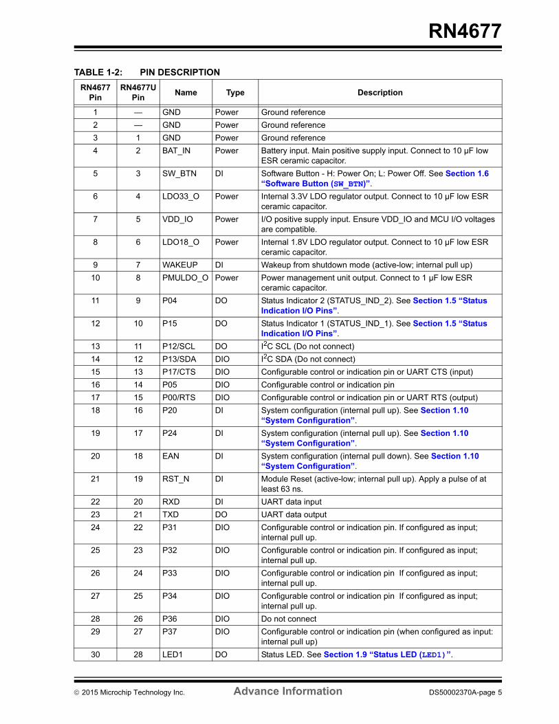
Figure 1-2 shows the RN4677 pin diagram and Figure 1-3 shows the RN4677U. Table 1-2 describes the module’s pins.
FIGURE 1-2: RN4677 PIN DIAGRAM
FIGURE 1-3: RN4677U PIN DIAGRAM
DS50002370A-page 4 Advance Information 2015 Microchip Technology Inc.
RN4677
TABLE 1-2: PIN DESCRIPTION
RN4677 Pin
RN4677U Pin
Name Type Description
1 — GND Power Ground reference
2 — GND Power Ground reference
3 1 GND Power Ground reference
4 2 BAT_IN Power Battery input. Main positive supply input. Connect to 10 µF low ESR ceramic capacitor.
5 3 SW_BTN DI Software Button - H: Power On; L: Power Off. See Section 1.6 “Software Button (SW_BTN)”.
6 4 LDO33_O Power Internal 3.3V LDO regulator output. Connect to 10 µF low ESR ceramic capacitor.
7 5 VDD_IO Power I/O positive supply input. Ensure VDD_IO and MCU I/O voltages are compatible.
8 6 LDO18_O Power Internal 1.8V LDO regulator output. Connect to 10 µF low ESR ceramic capacitor.
9 7 WAKEUP DI Wakeup from shutdown mode (active-low; internal pull up)
10 8 PMULDO_O Power Power management unit output. Connect to 1 µF low ESR ceramic capacitor.
11 9 P04 DO Status Indicator 2 (STATUS_IND_2). See Section 1.5 “Status Indication I/O Pins”.
12 10 P15 DO Status Indicator 1 (STATUS_IND_1). See Section 1.5 “Status Indication I/O Pins”.
13 11 P12/SCL DO I2C SCL (Do not connect)
14 12 P13/SDA DIO I2C SDA (Do not connect)
15 13 P17/CTS DIO Configurable control or indication pin or UART CTS (input)
16 14 P05 DIO Configurable control or indication pin
17 15 P00/RTS DIO Configurable control or indication pin or UART RTS (output)
18 16 P20 DI System configuration (internal pull up). See Section 1.10 “System Configuration”.
19 17 P24 DI System configuration (internal pull up). See Section 1.10 “System Configuration”.
20 18 EAN DI System configuration (internal pull down). See Section 1.10 “System Configuration”.
21 19 RST_N DI Module Reset (active-low; internal pull up). Apply a pulse of at least 63 ns.
22 20 RXD DI UART data input
23 21 TXD DO UART data output
24 22 P31 DIO Configurable control or indication pin. If configured as input; internal pull up.
25 23 P32 DIO Configurable control or indication pin. If configured as input; internal pull up.
26 24 P33 DIO Configurable control or indication pin If configured as input; internal pull up.
27 25 P34 DIO Configurable control or indication pin If configured as input; internal pull up.
28 26 P36 DIO Do not connect
29 27 P37 DIO Configurable control or indication pin (when configured as input: internal pull up)
30 28 LED1 DO Status LED. See Section 1.9 “Status LED (LED1)”.
2015 Microchip Technology Inc. Advance Information DS50002370A-page 5
RN4677
1.2 Configuring the RN4677
Configuring the RN4677 features are performed usingeither RN-style ASCII command documented in the“RN4677 Bluetooth® Low Energy Dual Mode ModuleUser’s Guide”. Alternatively, it is possible to configurethe RN4677 using the interface as described inSection 2.2 “External Configuration andProgramming”, along with either external PCconfiguration utility (UI Tool or EEPROM Tool), or thePIC MCU configuration library. For more information,visit www.microchip.com/rn4677.
1.3 UART Interface
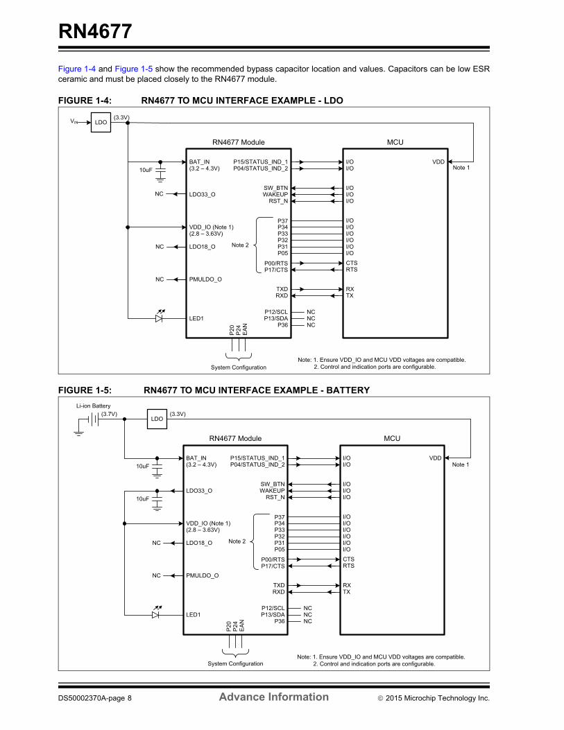
Figure 1-4 and Figure 1-5 show power and MCUinterface examples.
The RN4677 UART pins TXD and RXD connect to theUART pins of the host MCU. It is highly recommendedto use hardware flow control pins RTS and CTS. Bydefault, the RN4677 hardware flow control is disabledand must be configured to become enabled. The UARTBaud is configurable and the available signal rates arelisted in Table 4-5.
1.4 Control and Indication I/O Pins
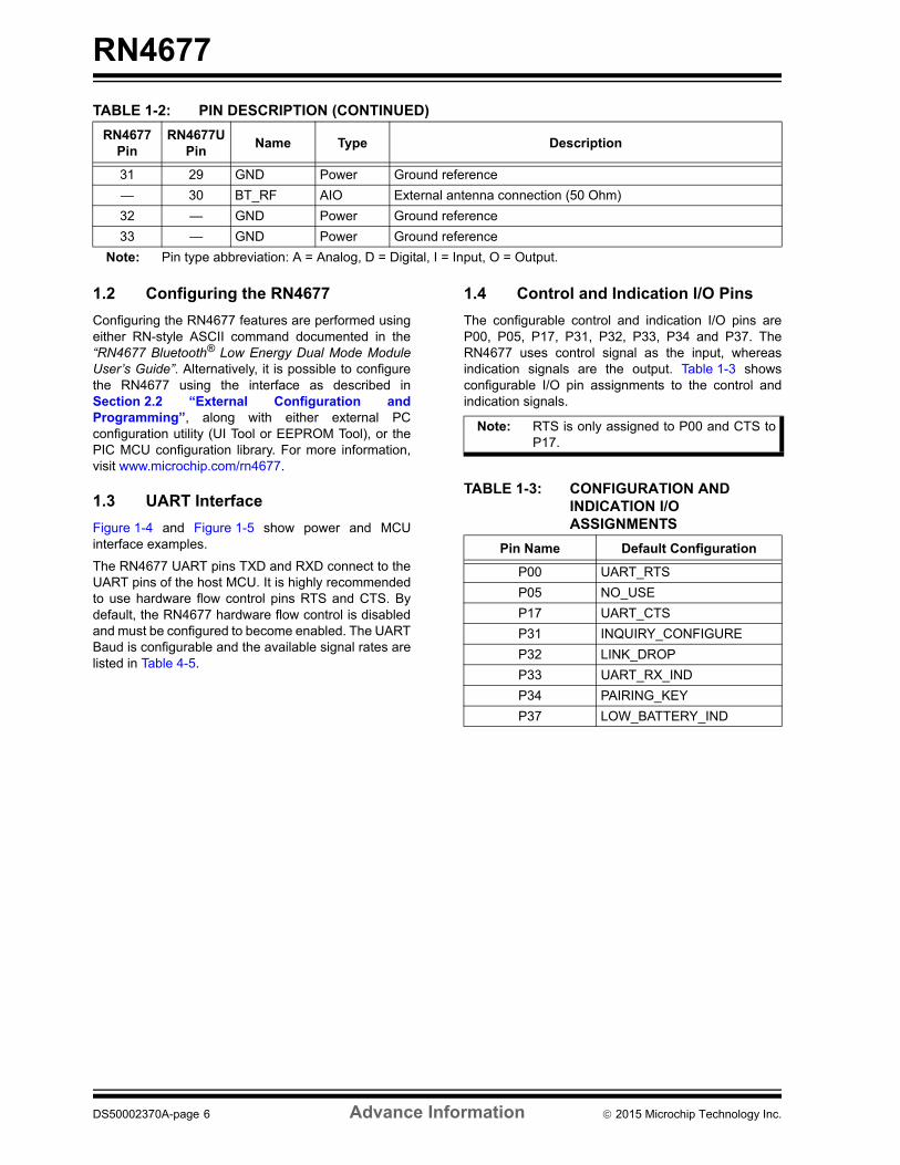
The configurable control and indication I/O pins areP00, P05, P17, P31, P32, P33, P34 and P37. TheRN4677 uses control signal as the input, whereasindication signals are the output. Table 1-3 showsconfigurable I/O pin assignments to the control andindication signals.
31 29 GND Power Ground reference
— 30 BT_RF AIO External antenna connection (50 Ohm)
32 — GND Power Ground reference
33 — GND Power Ground reference
Note: Pin type abbreviation: A = Analog, D = Digital, I = Input, O = Output.
TABLE 1-2: PIN DESCRIPTION (CONTINUED)
RN4677 Pin
RN4677U Pin
Name Type Description
Note: RTS is only assigned to P00 and CTS toP17.
TABLE 1-3: CONFIGURATION AND INDICATION I/O ASSIGNMENTS
Pin Name Default Configuration
P00 UART_RTS
P05 NO_USE
P17 UART_CTS
P31 INQUIRY_CONFIGURE
P32 LINK_DROP
P33 UART_RX_IND
P34 PAIRING_KEY
P37 LOW_BATTERY_IND
DS50002370A-page 6 Advance Information 2015 Microchip Technology Inc.
RN4677
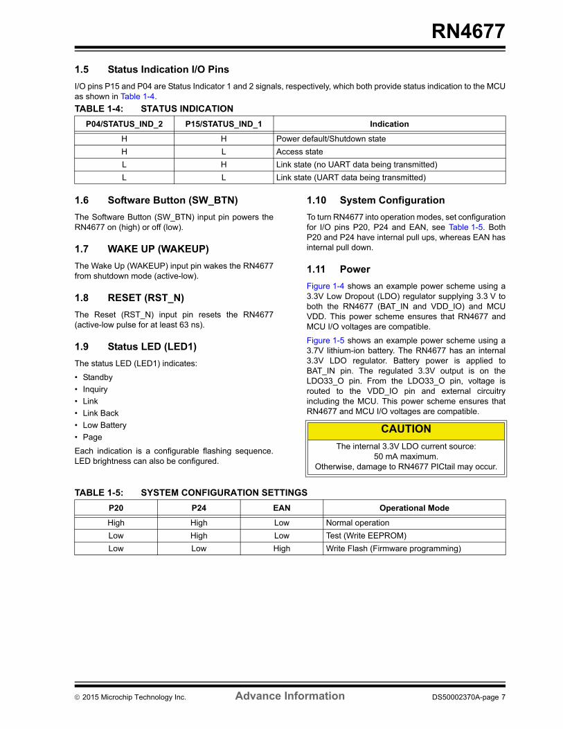
1.5 Status Indication I/O Pins
I/O pins P15 and P04 are Status Indicator 1 and 2 signals, respectively, which both provide status indication to the MCUas shown in Table 1-4.
1.6 Software Button (SW_BTN)
The Software Button (SW_BTN) input pin powers theRN4677 on (high) or off (low).
1.7 WAKE UP (WAKEUP)
The Wake Up (WAKEUP) input pin wakes the RN4677from shutdown mode (active-low).
1.8 RESET (RST_N)
The Reset (RST_N) input pin resets the RN4677(active-low pulse for at least 63 ns).
1.9 Status LED (LED1)
The status LED (LED1) indicates:
• Standby
• Inquiry
• Link
• Link Back
• Low Battery
• Page
Each indication is a configurable flashing sequence.LED brightness can also be configured.
1.10 System Configuration
To turn RN4677 into operation modes, set configurationfor I/O pins P20, P24 and EAN, see Table 1-5. BothP20 and P24 have internal pull ups, whereas EAN hasinternal pull down.
1.11 Power
Figure 1-4 shows an example power scheme using a3.3V Low Dropout (LDO) regulator supplying 3.3 V toboth the RN4677 (BAT_IN and VDD_IO) and MCUVDD. This power scheme ensures that RN4677 andMCU I/O voltages are compatible.
Figure 1-5 shows an example power scheme using a3.7V lithium-ion battery. The RN4677 has an internal3.3V LDO regulator. Battery power is applied toBAT_IN pin. The regulated 3.3V output is on theLDO33_O pin. From the LDO33_O pin, voltage isrouted to the VDD_IO pin and external circuitryincluding the MCU. This power scheme ensures thatRN4677 and MCU I/O voltages are compatible.
TABLE 1-4: STATUS INDICATION
P04/STATUS_IND_2 P15/STATUS_IND_1 Indication
H H Power default/Shutdown state
H L Access state
L H Link state (no UART data being transmitted)
L L Link state (UART data being transmitted)
CAUTION
The internal 3.3V LDO current source: 50 mA maximum.
Otherwise, damage to RN4677 PICtail may occur.
TABLE 1-5: SYSTEM CONFIGURATION SETTINGS
P20 P24 EAN Operational Mode
High High Low Normal operation
Low High Low Test (Write EEPROM)
Low Low High Write Flash (Firmware programming)
2015 Microchip Technology Inc. Advance Information DS50002370A-page 7
RN4677
Figure 1-4 and Figure 1-5 show the recommended bypass capacitor location and values. Capacitors can be low ESRceramic and must be placed closely to the RN4677 module.
FIGURE 1-4: RN4677 TO MCU INTERFACE EXAMPLE - LDO
FIGURE 1-5: RN4677 TO MCU INTERFACE EXAMPLE - BATTERY
Note: 1. Ensure VDD_IO and MCU VDD voltages are compatible.2. Control and indication ports are configurable.
Note 1
VIN
BAT_IN
RN4677 Module
(3.2 – 4.3V)
LDO33_O
VDD_IO (Note 1)
LDO18_O
SW_BTN
TXDRXD
WAKEUP
P24EAN
RST_N
P20
P12/SCLP13/SDA
P37P34P33P32P31
P04/STATUS_IND_2P15/STATUS_IND_1
PMULDO_O
MCU
VDDI/O
CTSRTS
RXTX
NC
(2.8 – 3.63V)
System Configuration
P05
P00/RTSP17/CTS
P36NCNC
I/O
I/OI/OI/O
I/OI/OI/OI/OI/OI/O
Note 2
LED1
10uF
NC
NC
NC
LDO(3.3V)
BAT_IN
RN4677 Module
(3.2 – 4.3V)
LDO33_O
VDD_IO (Note 1)
LDO18_O
SW_BTN
TXDRXD
WAKEUP
P24EAN
RST_N
P20
P12/SCLP13/SDA
P37P34P33P32P31
P04/STATUS_IND_2P15/STATUS_IND_1
PMULDO_O
MCU
VDDI/O
CTSRTS
RXTX
NC
(2.8 – 3.63V)
Li-ion Battery
System Configuration
P05
P00/RTSP17/CTS
P36NCNC
I/O
I/OI/OI/O
I/OI/OI/OI/OI/OI/O
(3.7V)
Note 2
Note: 1. Ensure VDD_IO and MCU VDD voltages are compatible.2. Control and indication ports are configurable.
Note 1
LED1
10uF
10uF
NC
NC
LDO(3.3V)
DS50002370A-page 8 Advance Information 2015 Microchip Technology Inc.
RN4677
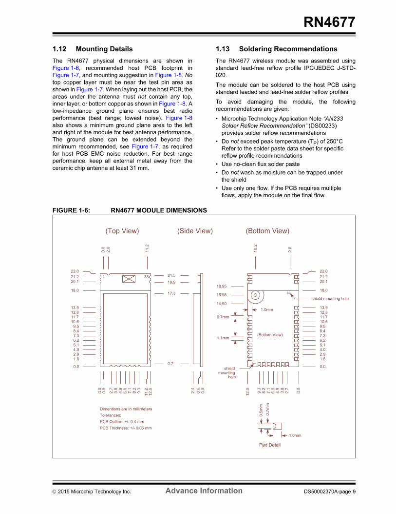
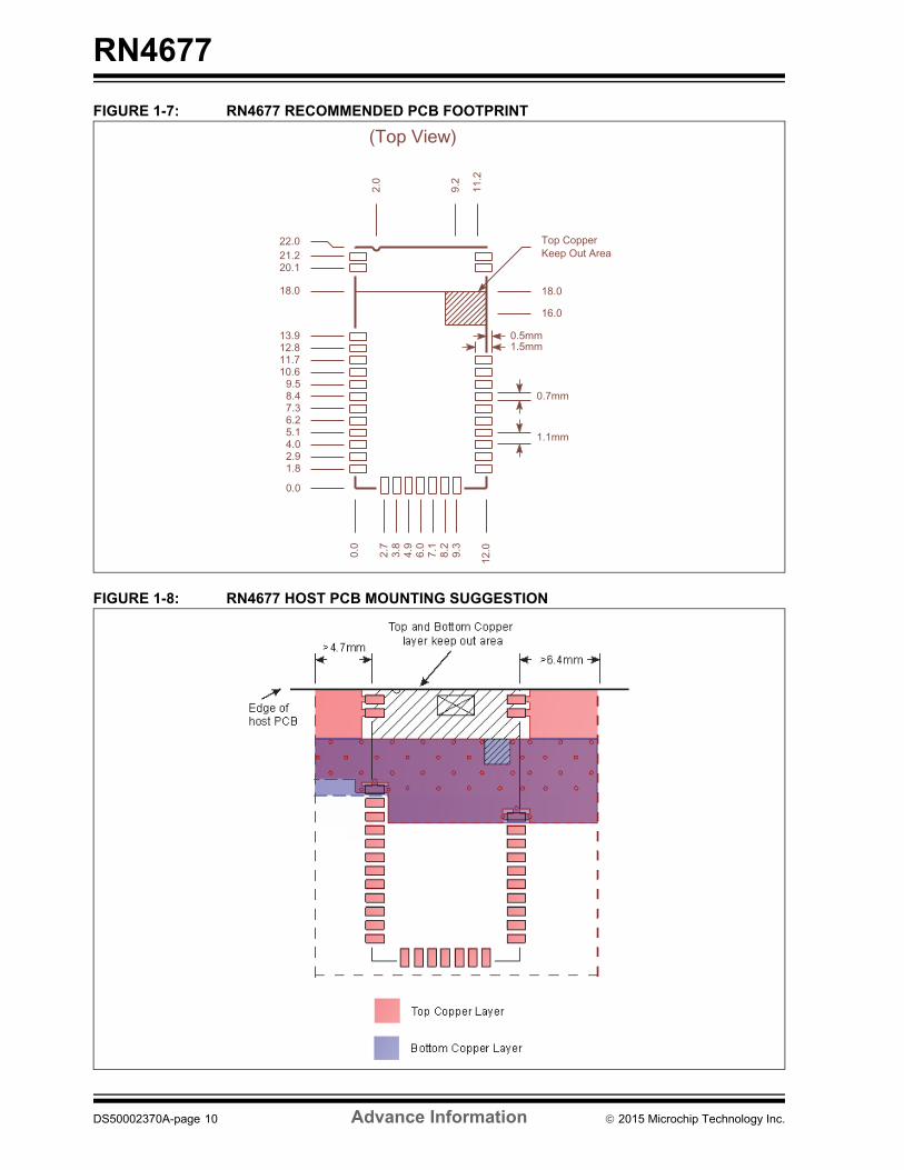
1.12 Mounting Details
The RN4677 physical dimensions are shown inFigure 1-6, recommended host PCB footprint inFigure 1-7, and mounting suggestion in Figure 1-8. Notop copper layer must be near the test pin area asshown in Figure 1-7. When laying out the host PCB, theareas under the antenna must not contain any top,inner layer, or bottom copper as shown in Figure 1-8. Alow-impedance ground plane ensures best radioperformance (best range; lowest noise). Figure 1-8also shows a minimum ground plane area to the leftand right of the module for best antenna performance.The ground plane can be extended beyond theminimum recommended, see Figure 1-7, as requiredfor host PCB EMC noise reduction. For best rangeperformance, keep all external metal away from theceramic chip antenna at least 31 mm.
1.13 Soldering Recommendations
The RN4677 wireless module was assembled usingstandard lead-free reflow profile IPC/JEDEC J-STD-020.
The module can be soldered to the host PCB usingstandard leaded and lead-free solder reflow profiles.
To avoid damaging the module, the followingrecommendations are given:
• Microchip Technology Application Note “AN233 Solder Reflow Recommendation” (DS00233) provides solder reflow recommendations
• Do not exceed peak temperature (TP) of 250°C Refer to the solder paste data sheet for specific reflow profile recommendations
• Use no-clean flux solder paste
• Do not wash as moisture can be trapped under the shield
• Use only one flow. If the PCB requires multiple flows, apply the module on the final flow.
FIGURE 1-6: RN4677 MODULE DIMENSIONS
2015 Microchip Technology Inc. Advance Information DS50002370A-page 9
RN4677
FIGURE 1-7: RN4677 RECOMMENDED PCB FOOTPRINT
FIGURE 1-8: RN4677 HOST PCB MOUNTING SUGGESTION
DS50002370A-page 10 Advance Information 2015 Microchip Technology Inc.
RN4677
2.0 APPLICATION INFORMATION
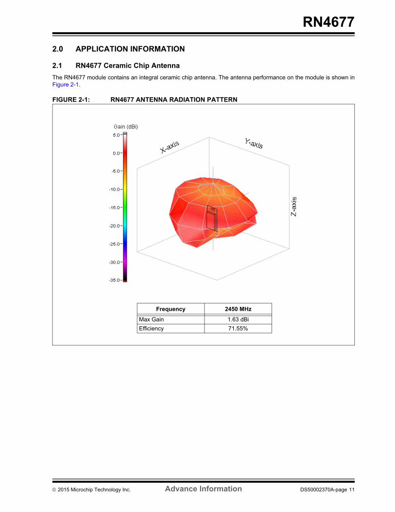
2.1 RN4677 Ceramic Chip Antenna
The RN4677 module contains an integral ceramic chip antenna. The antenna performance on the module is shown inFigure 2-1.
FIGURE 2-1: RN4677 ANTENNA RADIATION PATTERN
Frequency 2450 MHz
Max Gain 1.63 dBi
Efficiency 71.55%
2015 Microchip Technology Inc. Advance Information DS50002370A-page 11
RN4677
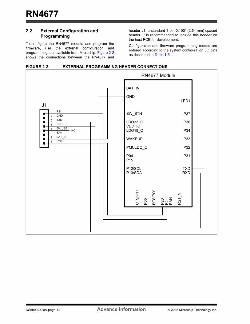
2.2 External Configuration and Programming
To configure the RN4677 module and program thefirmware, use the external configuration andprogramming tool available from Microchip. Figure 2-2shows the connections between the RN4677 and
header J1, a standard 8-pin 0.100" (2.54 mm) spacedheader. It is recommended to include this header onthe host PCB for development.
Configuration and firmware programming modes areentered according to the system configuration I/O pinsas described in Table 1-5.
FIGURE 2-2: EXTERNAL PROGRAMMING HEADER CONNECTIONS
12345678 P24
GNDTXDRXD5V_USBEANBAT_INP20
BAT_IN
RN4677 Module
LDO33_OVDD_IOLDO18_O
SW_BTN
TXDRXD
CTS/P17
RTS/P00
WAKEUP
LED1
P24EAN
RST_N
P20P12/SCLP13/SDA
P37
P36
P34
P33
P32
P31P04P15
PMULDO_OP05
GND
NC
J1
DS50002370A-page 12 Advance Information 2015 Microchip Technology Inc.
RN4677
3.0 REGULATORY APPROVAL
This section outlines the regulatory information for theRN4677 module for the following countries:
• United States
• Canada
• Europe
3.1 United States
The RN4677 module has received FederalCommunications Commission (FCC) CFR47Telecommunications, Part 15 Subpart C “IntentionalRadiators” modular approval in accordance with Part15.212 Modular Transmitter approval. Modularapproval allows the end user to integrate the RN4677module into a finished product without obtainingsubsequent and separate FCC approvals forintentional radiation, provided no changes ormodifications are made to the module circuitry.Changes or modifications could void the user'sauthority to operate the equipment. The end user mustcomply with all of the instructions provided by theGrantee, which indicate installation and/or operatingconditions necessary for compliance.
The finished product is required to comply with allapplicable FCC equipment authorizations regulations,requirements and equipment functions not associatedwith the transmitter module portion. For example,compliance must be demonstrated to regulations forother transmitter components within the host product;to requirements for unintentional radiators (Part 15Subpart B “Unintentional Radiators”), such as digitaldevices, computer peripherals, radio receivers, etc.;and to additional authorization requirements for thenon-transmitter functions on the transmitter module(i.e., Verification, or Declaration of Conformity) (e.g.,transmitter modules may also contain digital logicfunctions) as appropriate.
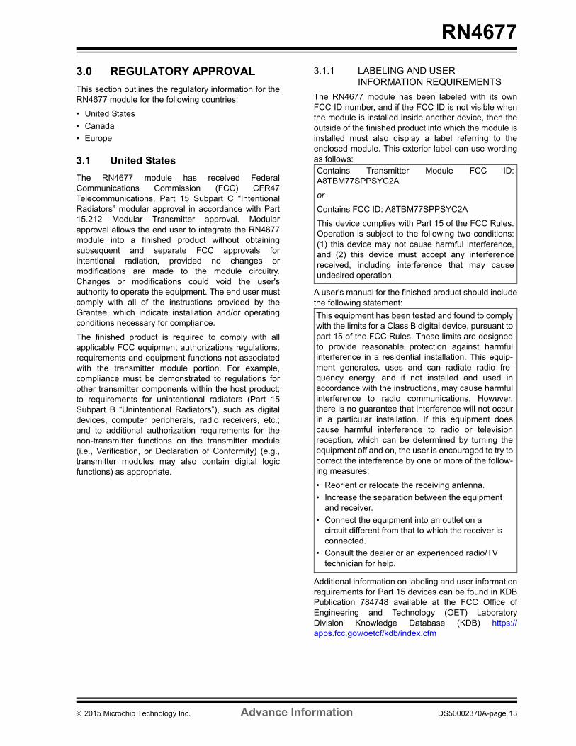
3.1.1 LABELING AND USER INFORMATION REQUIREMENTS
The RN4677 module has been labeled with its ownFCC ID number, and if the FCC ID is not visible whenthe module is installed inside another device, then theoutside of the finished product into which the module isinstalled must also display a label referring to theenclosed module. This exterior label can use wordingas follows:
A user's manual for the finished product should includethe following statement:
Additional information on labeling and user informationrequirements for Part 15 devices can be found in KDBPublication 784748 available at the FCC Office ofEngineering and Technology (OET) LaboratoryDivision Knowledge Database (KDB) https://apps.fcc.gov/oetcf/kdb/index.cfm
Contains Transmitter Module FCC ID:A8TBM77SPPSYC2A
or
Contains FCC ID: A8TBM77SPPSYC2A
This device complies with Part 15 of the FCC Rules.Operation is subject to the following two conditions:(1) this device may not cause harmful interference,and (2) this device must accept any interferencereceived, including interference that may causeundesired operation.
This equipment has been tested and found to complywith the limits for a Class B digital device, pursuant topart 15 of the FCC Rules. These limits are designedto provide reasonable protection against harmfulinterference in a residential installation. This equip-ment generates, uses and can radiate radio fre-quency energy, and if not installed and used inaccordance with the instructions, may cause harmfulinterference to radio communications. However,there is no guarantee that interference will not occurin a particular installation. If this equipment doescause harmful interference to radio or televisionreception, which can be determined by turning theequipment off and on, the user is encouraged to try tocorrect the interference by one or more of the follow-ing measures:
• Reorient or relocate the receiving antenna.
• Increase the separation between the equipment and receiver.
• Connect the equipment into an outlet on a circuit different from that to which the receiver is connected.
• Consult the dealer or an experienced radio/TV technician for help.
2015 Microchip Technology Inc. Advance Information DS50002370A-page 13
RN4677
3.1.2 RF EXPOSURE
All transmitters regulated by FCC must comply with RFexposure requirements. KDB 447498 General RFExposure Guidance provides guidance in determiningwhether proposed or existing transmitting facilities,operations or devices comply with limits for humanexposure to Radio Frequency (RF) fields adopted bythe Federal Communications Commission (FCC).
From the RN4677 FCC Grant: Output power listed isconducted. This grant is valid only when the module issold to OEM integrators and must be installed by theOEM or OEM integrators. This transmitter is restrictedfor use with the specific antenna(s) tested in thisapplication for Certification and must not be co-locatedor operating in conjunction with any other antenna ortransmitters within a host device, except in accordancewith FCC multi-transmitter product procedures.
3.1.3 HELPFUL WEB SITES
Federal Communications Commission (FCC): http://www.fcc.gov
FCC Office of Engineering and Technology (OET)Laboratory Division Knowledge Database (KDB):https://apps.fcc.gov/oetcf/kdb/index.cfm
3.2 Canada
The RN4677 module has been certified for use inCanada under Industry Canada (IC) Radio StandardsSpecification (RSS) RSS-210 and RSS-Gen. Modularapproval permits the installation of a module in a hostdevice without the need to recertify the device.
3.2.1 LABELING AND USER INFORMATION REQUIREMENTS
Labeling Requirements for the Host Device (fromSection 3.2.1, RSS-Gen, Issue 3, December 2010):The host device shall be properly labeled to identify themodule within the host device.
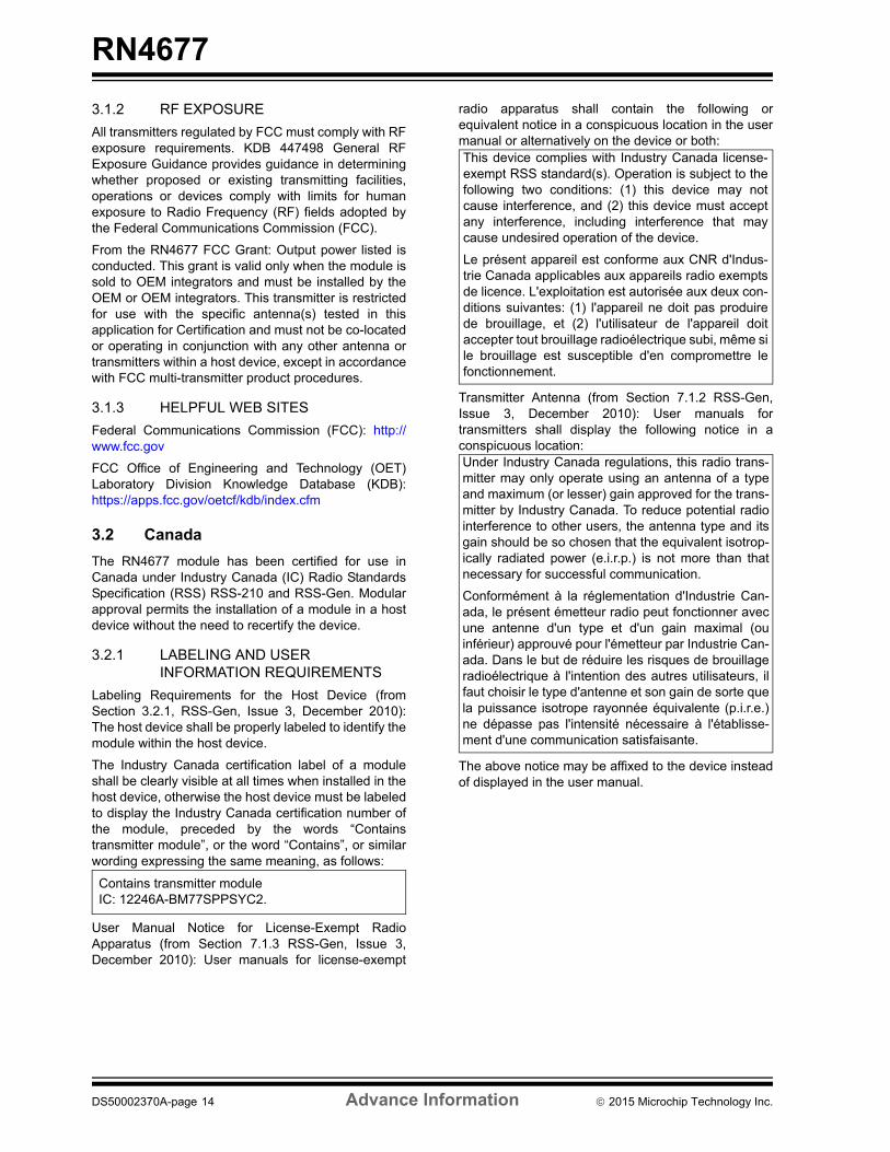
The Industry Canada certification label of a moduleshall be clearly visible at all times when installed in thehost device, otherwise the host device must be labeledto display the Industry Canada certification number ofthe module, preceded by the words “Containstransmitter module”, or the word “Contains”, or similarwording expressing the same meaning, as follows:
User Manual Notice for License-Exempt RadioApparatus (from Section 7.1.3 RSS-Gen, Issue 3,December 2010): User manuals for license-exempt
radio apparatus shall contain the following orequivalent notice in a conspicuous location in the usermanual or alternatively on the device or both:
Transmitter Antenna (from Section 7.1.2 RSS-Gen,Issue 3, December 2010): User manuals fortransmitters shall display the following notice in aconspicuous location:
The above notice may be affixed to the device insteadof displayed in the user manual.
Contains transmitter module IC: 12246A-BM77SPPSYC2.
This device complies with Industry Canada license-exempt RSS standard(s). Operation is subject to thefollowing two conditions: (1) this device may notcause interference, and (2) this device must acceptany interference, including interference that maycause undesired operation of the device.
Le présent appareil est conforme aux CNR d'Indus-trie Canada applicables aux appareils radio exemptsde licence. L'exploitation est autorisée aux deux con-ditions suivantes: (1) l'appareil ne doit pas produirede brouillage, et (2) l'utilisateur de l'appareil doitaccepter tout brouillage radioélectrique subi, même sile brouillage est susceptible d'en compromettre lefonctionnement.
Under Industry Canada regulations, this radio trans-mitter may only operate using an antenna of a typeand maximum (or lesser) gain approved for the trans-mitter by Industry Canada. To reduce potential radiointerference to other users, the antenna type and itsgain should be so chosen that the equivalent isotrop-ically radiated power (e.i.r.p.) is not more than thatnecessary for successful communication.
Conformément à la réglementation d'Industrie Can-ada, le présent émetteur radio peut fonctionner avecune antenne d'un type et d'un gain maximal (ouinférieur) approuvé pour l'émetteur par Industrie Can-ada. Dans le but de réduire les risques de brouillageradioélectrique à l'intention des autres utilisateurs, ilfaut choisir le type d'antenne et son gain de sorte quela puissance isotrope rayonnée équivalente (p.i.r.e.)ne dépasse pas l'intensité nécessaire à l'établisse-ment d'une communication satisfaisante.
DS50002370A-page 14 Advance Information 2015 Microchip Technology Inc.
RN4677
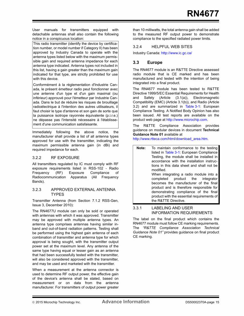
User manuals for transmitters equipped withdetachable antennas shall also contain the followingnotice in a conspicuous location:
Immediately following the above notice, themanufacturer shall provide a list of all antenna typesapproved for use with the transmitter, indicating themaximum permissible antenna gain (in dBi) andrequired impedance for each.
3.2.2 RF EXPOSURE
All transmitters regulated by IC must comply with RFexposure requirements listed in RSS-102 - RadioFrequency (RF) Exposure Compliance ofRadiocommunication Apparatus (All FrequencyBands).
3.2.3 APPROVED EXTERNAL ANTENNA TYPES
Transmitter Antenna (from Section 7.1.2 RSS-Gen,Issue 3, December 2010):
The RN4677U module can only be sold or operatedwith antennas with which it was approved. Transmittermay be approved with multiple antenna types. Anantenna type comprises antennas having similar in-band and out-of-band radiation patterns. Testing shallbe performed using the highest gain antenna of eachcombination of transmitter and antenna type for whichapproval is being sought, with the transmitter outputpower set at the maximum level. Any antenna of thesame type having equal or lesser gain as an antennathat had been successfully tested with the transmitter,will also be considered approved with the transmitter,and may be used and marketed with the transmitter.
When a measurement at the antenna connector isused to determine RF output power, the effective gainof the device's antenna shall be stated, based onmeasurement or on data from the antennamanufacturer. For transmitters of output power greater
than 10 milliwatts, the total antenna gain shall be addedto the measured RF output power to demonstratecompliance to the specified radiated power limits.
3.2.4 HELPFUL WEB SITES
Industry Canada: http://www.ic.gc.ca/
3.3 Europe
The RN4677 module is an R&TTE Directive assessedradio module that is CE marked and has beenmanufactured and tested with the intention of beingintegrated into a final product.
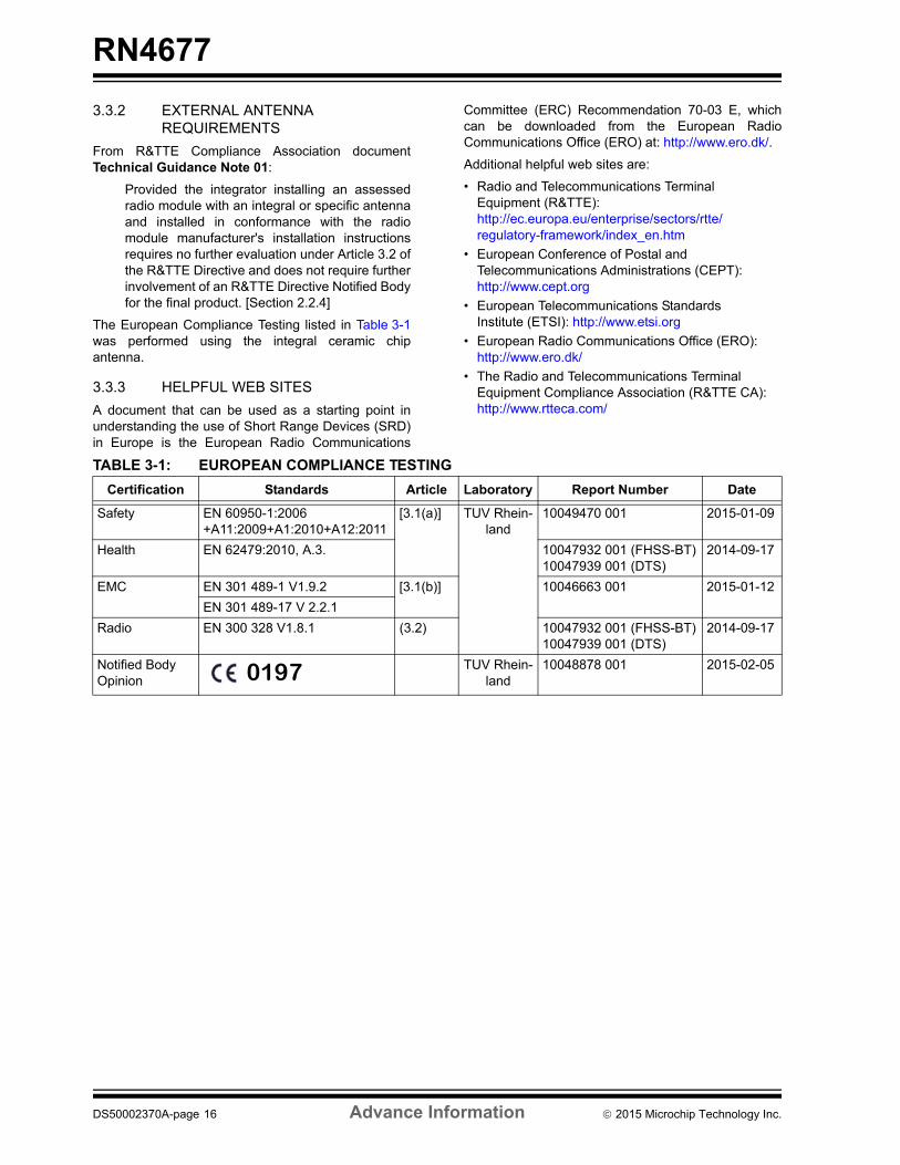
The RN4677 module has been tested to R&TTEDirective 1999/5/EC Essential Requirements for Healthand Safety (Article (3.1(a)), ElectromagneticCompatibility (EMC) (Article 3.1(b)), and Radio (Article3.2) and are summarized in Table 3-1: EuropeanCompliance Testing. A Notified Body Opinion has alsobeen issued. All test reports are available on theproduct web page at http://www.microchip.com.
The R&TTE Compliance Association providesguidance on modular devices in document TechnicalGuidance Note 01 available at http://www.rtteca.com/html/download_area.htm.
3.3.1 LABELING AND USER INFORMATION REQUIREMENTS
The label on the final product which contains theRN4677 module must follow CE marking requirements.The “R&TTE Compliance Association TechnicalGuidance Note 01” provides guidance on final productCE marking.
This radio transmitter (identify the device by certifica-tion number, or model number if Category II) has beenapproved by Industry Canada to operate with theantenna types listed below with the maximum permis-sible gain and required antenna impedance for eachantenna type indicated. Antenna types not included inthis list, having a gain greater than the maximum gainindicated for that type, are strictly prohibited for usewith this device.
Conformément à la réglementation d'Industrie Can-ada, le présent émetteur radio peut fonctionner avecune antenne d'un type et d'un gain maximal (ouinférieur) approuvé pour l'émetteur par Industrie Can-ada. Dans le but de réduire les risques de brouillageradioélectrique à l'intention des autres utilisateurs, ilfaut choisir le type d'antenne et son gain de sorte quela puissance isotrope rayonnée équivalente (p.i.r.e.)ne dépasse pas l'intensité nécessaire à l'établisse-ment d'une communication satisfaisante.
Note: To maintain conformance to the testinglisted in Table 3-1: European ComplianceTesting, the module shall be installed inaccordance with the installation instruc-tions in this data sheet and shall not bemodified. When integrating a radio module into acompleted product the integratorbecomes the manufacturer of the finalproduct and is therefore responsible fordemonstrating compliance of the finalproduct with the essential requirements ofthe R&TTE Directive.
2015 Microchip Technology Inc. Advance Information DS50002370A-page 15
RN4677
3.3.2 EXTERNAL ANTENNA REQUIREMENTS
From R&TTE Compliance Association documentTechnical Guidance Note 01:
Provided the integrator installing an assessedradio module with an integral or specific antennaand installed in conformance with the radiomodule manufacturer's installation instructionsrequires no further evaluation under Article 3.2 ofthe R&TTE Directive and does not require furtherinvolvement of an R&TTE Directive Notified Bodyfor the final product. [Section 2.2.4]
The European Compliance Testing listed in Table 3-1was performed using the integral ceramic chipantenna.
3.3.3 HELPFUL WEB SITES
A document that can be used as a starting point inunderstanding the use of Short Range Devices (SRD)in Europe is the European Radio Communications
Committee (ERC) Recommendation 70-03 E, whichcan be downloaded from the European RadioCommunications Office (ERO) at: http://www.ero.dk/.
Additional helpful web sites are:
• Radio and Telecommunications Terminal Equipment (R&TTE): http://ec.europa.eu/enterprise/sectors/rtte/regulatory-framework/index_en.htm
• European Conference of Postal and Telecommunications Administrations (CEPT): http://www.cept.org
• European Telecommunications Standards Institute (ETSI): http://www.etsi.org
• European Radio Communications Office (ERO): http://www.ero.dk/
• The Radio and Telecommunications Terminal Equipment Compliance Association (R&TTE CA):http://www.rtteca.com/
TABLE 3-1: EUROPEAN COMPLIANCE TESTING
Certification Standards Article Laboratory Report Number Date
Safety EN 60950-1:2006+A11:2009+A1:2010+A12:2011
[3.1(a)] TUV Rhein-land
10049470 001 2015-01-09
Health EN 62479:2010, A.3. 10047932 001 (FHSS-BT)10047939 001 (DTS)
2014-09-17
EMC EN 301 489-1 V1.9.2 [3.1(b)] 10046663 001 2015-01-12
EN 301 489-17 V 2.2.1
Radio EN 300 328 V1.8.1 (3.2) 10047932 001 (FHSS-BT)10047939 001 (DTS)
2014-09-17
Notified Body Opinion
TUV Rhein-land
10048878 001 2015-02-050197
DS50002370A-page 16 Advance Information 2015 Microchip Technology Inc.
RN4677
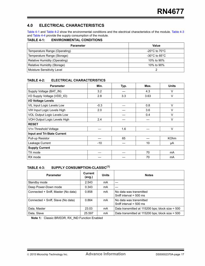
4.0 ELECTRICAL CHARACTERISTICS
Table 4-1 and Table 4-2 show the environmental conditions and the electrical characteristics of the module. Table 4-3and Table 4-4 provide the supply consumption of the module.
TABLE 4-1: ENVIRONMENTAL CONDITIONS
Parameter Value
Temperature Range (Operating) -20°C to 70°C
Temperature Range (Storage) -30°C to 85°C
Relative Humidity (Operating) 10% to 90%
Relative Humidity (Storage) 10% to 90%
Moisture Sensitivity Level 2
TABLE 4-2: ELECTRICAL CHARACTERISTICS
Parameter Min. Typ. Max. Units
Supply Voltage (BAT_IN) 3.2 — 4.3 V
I/O Supply Voltage (VDD_IO) 2.8 3.3 3.63 V
I/O Voltage Levels
VIL Input Logic Levels Low -0.3 — 0.8 V
VIH Input Logic Levels High 2.0 — 3.6 V
VOL Output Logic Levels Low — 0.4 V
VOH Output Logic Levels High 2.4 — — V
RESET
VTH Threshold Voltage — 1.6 — V
Input and Tri-State Current
Pull-up Resistor — 65 — KOhm
Leakage Current -10 — 10 µA
Supply Current
TX mode — — 70 mA
RX mode — — 70 mA
TABLE 4-3: SUPPLY CONSUMPTION-CLASSIC(1)
ParameterCurrent (avg.)
Units Notes
Standby mode 2.543 mA —
Deep Power-Down mode 0.343 mA —
Connected + Sniff, Master (No data) 0.858 mA No data was transmitted Sniff interval = 500 ms
Connected + Sniff, Slave (No data) 0.864 mA No data was transmitted Sniff interval = 500 ms
Data, Master 23.03 mA Data transmitted at 115200 bps; block size = 500
Data, Slave 25.597 mA Data transmitted at 115200 bps; block size = 500
Note 1: Classic BR/EDR, RX_IND Function Enabled
2015 Microchip Technology Inc. Advance Information DS50002370A-page 17
RN4677
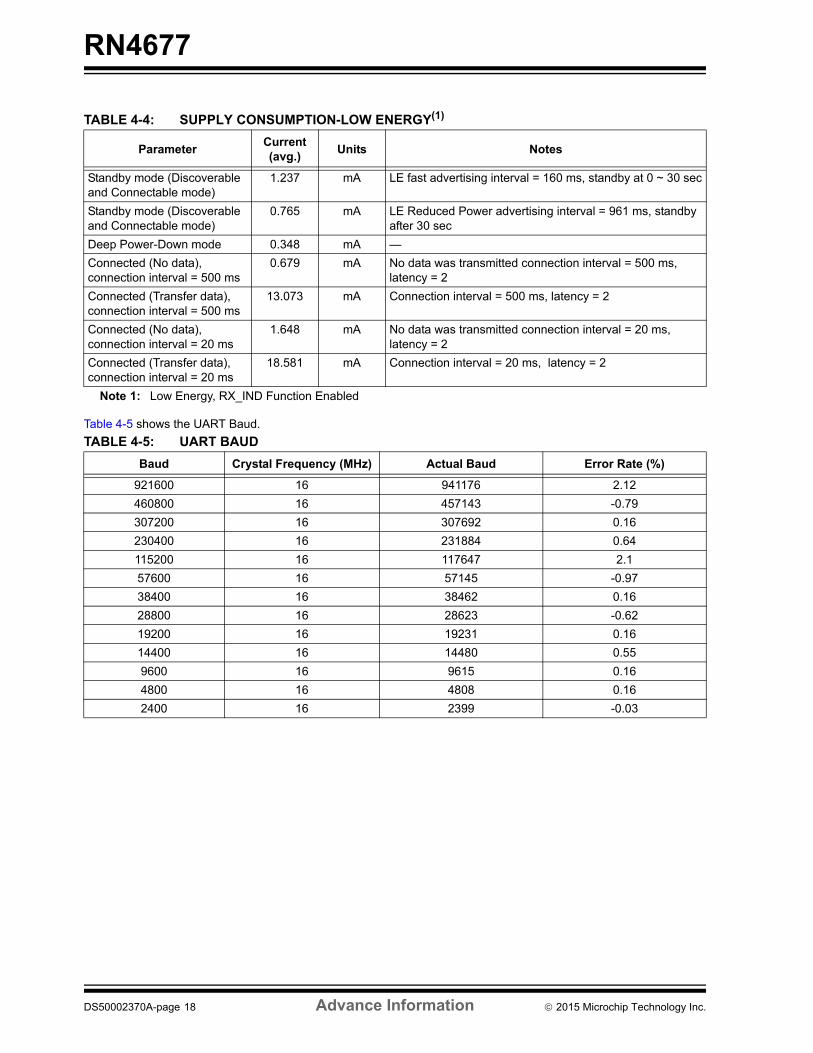
Table 4-5 shows the UART Baud.
TABLE 4-4: SUPPLY CONSUMPTION-LOW ENERGY(1)
ParameterCurrent (avg.)
Units Notes
Standby mode (Discoverable and Connectable mode)
1.237 mA LE fast advertising interval = 160 ms, standby at 0 ~ 30 sec
Standby mode (Discoverable and Connectable mode)
0.765 mA LE Reduced Power advertising interval = 961 ms, standby after 30 sec
Deep Power-Down mode 0.348 mA —
Connected (No data), connection interval = 500 ms
0.679 mA No data was transmitted connection interval = 500 ms, latency = 2
Connected (Transfer data), connection interval = 500 ms
13.073 mA Connection interval = 500 ms, latency = 2
Connected (No data), connection interval = 20 ms
1.648 mA No data was transmitted connection interval = 20 ms, latency = 2
Connected (Transfer data), connection interval = 20 ms
18.581 mA Connection interval = 20 ms, latency = 2
Note 1: Low Energy, RX_IND Function Enabled
TABLE 4-5: UART BAUD
Baud Crystal Frequency (MHz) Actual Baud Error Rate (%)
921600 16 941176 2.12
460800 16 457143 -0.79
307200 16 307692 0.16
230400 16 231884 0.64
115200 16 117647 2.1
57600 16 57145 -0.97
38400 16 38462 0.16
28800 16 28623 -0.62
19200 16 19231 0.16
14400 16 14480 0.55
9600 16 9615 0.16
4800 16 4808 0.16
2400 16 2399 -0.03
DS50002370A-page 18 Advance Information 2015 Microchip Technology Inc.
RN4677
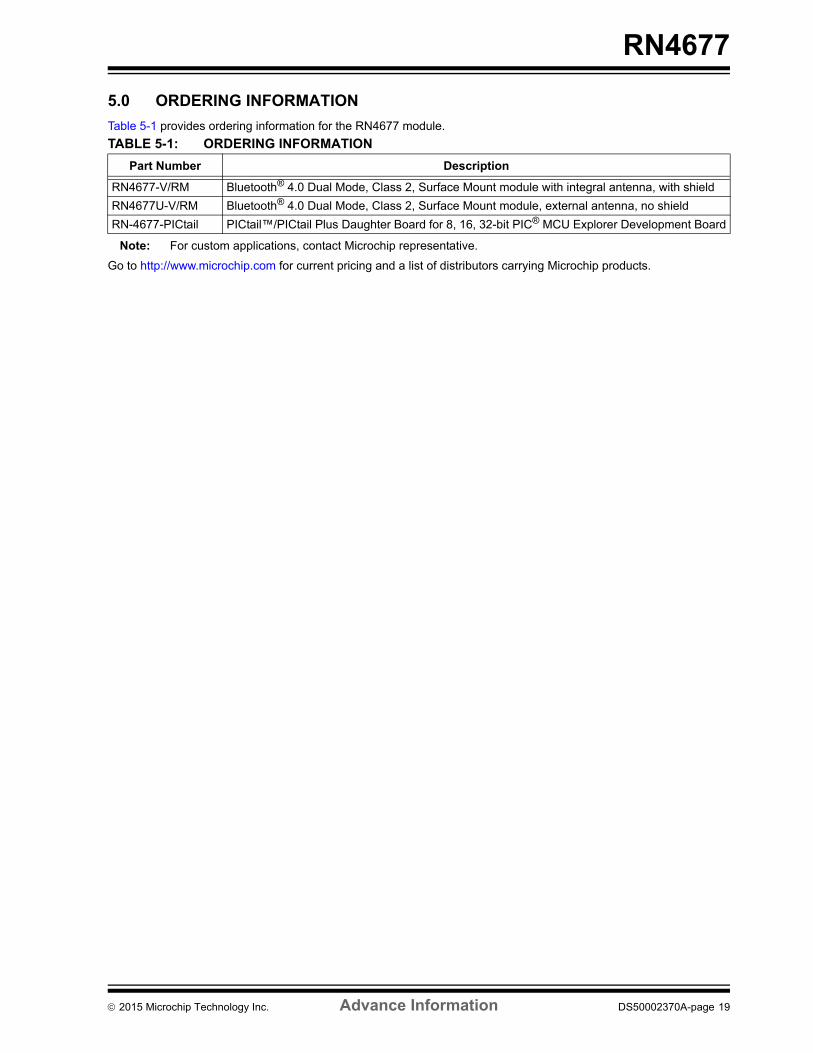
5.0 ORDERING INFORMATION
Table 5-1 provides ordering information for the RN4677 module.
Note: For custom applications, contact Microchip representative.
Go to http://www.microchip.com for current pricing and a list of distributors carrying Microchip products.
TABLE 5-1: ORDERING INFORMATION
Part Number Description
RN4677-V/RM Bluetooth® 4.0 Dual Mode, Class 2, Surface Mount module with integral antenna, with shield
RN4677U-V/RM Bluetooth® 4.0 Dual Mode, Class 2, Surface Mount module, external antenna, no shield
RN-4677-PICtail PICtail™/PICtail Plus Daughter Board for 8, 16, 32-bit PIC® MCU Explorer Development Board
2015 Microchip Technology Inc. Advance Information DS50002370A-page 19

RN4677
NOTES:
DS50002370A-page 20 Advance Information 2015 Microchip Technology Inc.
RN4677
APPENDIX A: REVISION HISTORY
Revision A (May 2015)
This is the initial release of this document.
2015 Microchip Technology Inc. Advance Information DS00000A-page 21
RN4677
NOTES:
DS00000A-page 22 Advance Information 2015 Microchip Technology Inc.
RN4677
THE MICROCHIP WEB SITE
Microchip provides online support via our WWW site atwww.microchip.com. This web site is used as a meansto make files and information easily available tocustomers. Accessible by using your favorite Internetbrowser, the web site contains the followinginformation:
• Product Support – Data sheets and errata, application notes and sample programs, design resources, user’s guides and hardware support documents, latest software releases and archived software
• General Technical Support – Frequently Asked Questions (FAQ), technical support requests, online discussion groups, Microchip consultant program member listing
• Business of Microchip – Product selector and ordering guides, latest Microchip press releases, listing of seminars and events, listings of Microchip sales offices, distributors and factory representatives
CUSTOMER CHANGE NOTIFICATION SERVICE
Microchip’s customer notification service helps keepcustomers current on Microchip products. Subscriberswill receive e-mail notification whenever there arechanges, updates, revisions or errata related to aspecified product family or development tool of interest.
To register, access the Microchip web site atwww.microchip.com. Under “Support”, click on“Customer Change Notification” and follow theregistration instructions.
CUSTOMER SUPPORT
Users of Microchip products can receive assistancethrough several channels:
• Distributor or Representative
• Local Sales Office
• Field Application Engineer (FAE)
• Technical Support
Customers should contact their distributor,representative or Field Application Engineer (FAE) forsupport. Local sales offices are also available to helpcustomers. A listing of sales offices and locations isincluded in the back of this document.
Technical support is available through the web siteat: http://microchip.com/support
2015 Microchip Technology Inc. DS50002370A-page 23
RN4677
NOTES:
DS50002370A-page 24 2015 Microchip Technology Inc.
RN4677
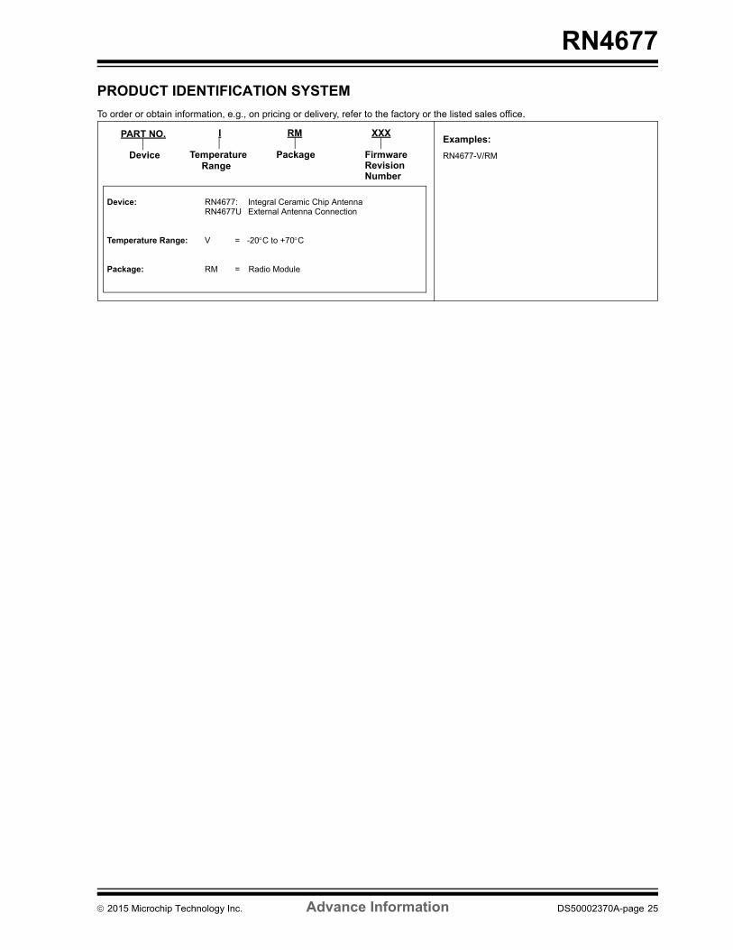
PRODUCT IDENTIFICATION SYSTEM
To order or obtain information, e.g., on pricing or delivery, refer to the factory or the listed sales office.
PART NO. I RM XXX
FirmwarePackageTemperatureRange
Device
Device: RN4677: Integral Ceramic Chip AntennaRN4677U External Antenna Connection
Temperature Range: V = -20C to +70C
Package: RM = Radio Module
Examples:
RN4677-V/RMRevisionNumber
2015 Microchip Technology Inc. Advance Information DS50002370A-page 25
RN4677
NOTES:
DS50002370A-page 26 Advance Information 2015 Microchip Technology Inc.
Note the following details of the code protection feature on Microchip devices:
• Microchip products meet the specification contained in their particular Microchip Data Sheet.
• Microchip believes that its family of products is one of the most secure families of its kind on the market today, when used in the intended manner and under normal conditions.
• There are dishonest and possibly illegal methods used to breach the code protection feature. All of these methods, to our knowledge, require using the Microchip products in a manner outside the operating specifications contained in Microchip’s Data Sheets. Most likely, the person doing so is engaged in theft of intellectual property.
• Microchip is willing to work with the customer who is concerned about the integrity of their code.
• Neither Microchip nor any other semiconductor manufacturer can guarantee the security of their code. Code protection does not mean that we are guaranteeing the product as “unbreakable.”
Code protection is constantly evolving. We at Microchip are committed to continuously improving the code protection features of ourproducts. Attempts to break Microchip’s code protection feature may be a violation of the Digital Millennium Copyright Act. If such actsallow unauthorized access to your software or other copyrighted work, you may have a right to sue for relief under that Act.
Information contained in this publication regarding deviceapplications and the like is provided only for your convenienceand may be superseded by updates. It is your responsibility toensure that your application meets with your specifications.MICROCHIP MAKES NO REPRESENTATIONS ORWARRANTIES OF ANY KIND WHETHER EXPRESS ORIMPLIED, WRITTEN OR ORAL, STATUTORY OROTHERWISE, RELATED TO THE INFORMATION,INCLUDING BUT NOT LIMITED TO ITS CONDITION,QUALITY, PERFORMANCE, MERCHANTABILITY ORFITNESS FOR PURPOSE. Microchip disclaims all liabilityarising from this information and its use. Use of Microchipdevices in life support and/or safety applications is entirely atthe buyer’s risk, and the buyer agrees to defend, indemnify andhold harmless Microchip from any and all damages, claims,suits, or expenses resulting from such use. No licenses areconveyed, implicitly or otherwise, under any Microchipintellectual property rights.
2015 Microchip Technology Inc. Advance Info
QUALITYMANAGEMENTSYSTEMCERTIFIEDBYDNV
== ISO/TS16949==
Trademarks
The Microchip name and logo, the Microchip logo, dsPIC, FlashFlex, flexPWR, JukeBlox, KEELOQ, KEELOQ logo, Kleer, LANCheck, MediaLB, MOST, MOST logo, MPLAB, OptoLyzer, PIC, PICSTART, PIC32 logo, RightTouch, SpyNIC, SST, SST Logo, SuperFlash and UNI/O are registered trademarks of Microchip Technology Incorporated in the U.S.A. and other countries.
The Embedded Control Solutions Company and mTouch are registered trademarks of Microchip Technology Incorporated in the U.S.A.
Analog-for-the-Digital Age, BodyCom, chipKIT, chipKIT logo, CodeGuard, dsPICDEM, dsPICDEM.net, ECAN, In-Circuit Serial Programming, ICSP, Inter-Chip Connectivity, KleerNet, KleerNet logo, MiWi, MPASM, MPF, MPLAB Certified logo, MPLIB, MPLINK, MultiTRAK, NetDetach, Omniscient Code Generation, PICDEM, PICDEM.net, PICkit, PICtail, RightTouch logo, REAL ICE, SQI, Serial Quad I/O, Total Endurance, TSHARC, USBCheck, VariSense, ViewSpan, WiperLock, Wireless DNA, and ZENA are trademarks of Microchip Technology Incorporated in the U.S.A. and other countries.
SQTP is a service mark of Microchip Technology Incorporated in the U.S.A.
Silicon Storage Technology is a registered trademark of Microchip Technology Inc. in other countries.
GestIC is a registered trademarks of Microchip Technology Germany II GmbH & Co. KG, a subsidiary of Microchip Technology Inc., in other countries.
All other trademarks mentioned herein are property of their respective companies.
© 2015, Microchip Technology Incorporated, Printed in the U.S.A., All Rights Reserved.
ISBN: 978-1-63277-382-1
rmation DS50002370A-page 27
Microchip received ISO/TS-16949:2009 certification for its worldwide headquarters, design and wafer fabrication facilities in Chandler and Tempe, Arizona; Gresham, Oregon and design centers in California and India. The Company’s quality system processes and procedures are for its PIC® MCUs and dsPIC® DSCs, KEELOQ® code hopping devices, Serial EEPROMs, microperipherals, nonvolatile memory and analog products. In addition, Microchip’s quality system for the design and manufacture of development systems is ISO 9001:2000 certified.
DS50002370A-page 28 2015 Microchip Technology Inc.
AMERICASCorporate Office2355 West Chandler Blvd.Chandler, AZ 85224-6199Tel: 480-792-7200 Fax: 480-792-7277Technical Support: http://www.microchip.com/supportWeb Address: www.microchip.com
AtlantaDuluth, GA Tel: 678-957-9614 Fax: 678-957-1455
Austin, TXTel: 512-257-3370
BostonWestborough, MA Tel: 774-760-0087 Fax: 774-760-0088
ChicagoItasca, IL Tel: 630-285-0071 Fax: 630-285-0075
ClevelandIndependence, OH Tel: 216-447-0464 Fax: 216-447-0643
DallasAddison, TX Tel: 972-818-7423 Fax: 972-818-2924
DetroitNovi, MI Tel: 248-848-4000
Houston, TX Tel: 281-894-5983Indianapolis
Noblesville, IN Tel: 317-773-8323Fax: 317-773-5453
Los AngelesMission Viejo, CA Tel: 949-462-9523 Fax: 949-462-9608
New York, NY Tel: 631-435-6000
San Jose, CA Tel: 408-735-9110
Canada - TorontoTel: 905-673-0699 Fax: 905-673-6509
ASIA/PACIFICAsia Pacific OfficeSuites 3707-14, 37th FloorTower 6, The GatewayHarbour City, Kowloon
Hong KongTel: 852-2943-5100Fax: 852-2401-3431
Australia - SydneyTel: 61-2-9868-6733Fax: 61-2-9868-6755
China - BeijingTel: 86-10-8569-7000 Fax: 86-10-8528-2104
China - ChengduTel: 86-28-8665-5511Fax: 86-28-8665-7889
China - ChongqingTel: 86-23-8980-9588Fax: 86-23-8980-9500
China - DongguanTel: 86-769-8702-9880
China - HangzhouTel: 86-571-8792-8115 Fax: 86-571-8792-8116
China - Hong Kong SARTel: 852-2943-5100 Fax: 852-2401-3431
China - NanjingTel: 86-25-8473-2460Fax: 86-25-8473-2470
China - QingdaoTel: 86-532-8502-7355Fax: 86-532-8502-7205
China - ShanghaiTel: 86-21-5407-5533 Fax: 86-21-5407-5066
China - ShenyangTel: 86-24-2334-2829Fax: 86-24-2334-2393
China - ShenzhenTel: 86-755-8864-2200 Fax: 86-755-8203-1760
China - WuhanTel: 86-27-5980-5300Fax: 86-27-5980-5118
China - XianTel: 86-29-8833-7252Fax: 86-29-8833-7256
ASIA/PACIFICChina - XiamenTel: 86-592-2388138 Fax: 86-592-2388130
China - ZhuhaiTel: 86-756-3210040 Fax: 86-756-3210049
India - BangaloreTel: 91-80-3090-4444 Fax: 91-80-3090-4123
India - New DelhiTel: 91-11-4160-8631Fax: 91-11-4160-8632
India - PuneTel: 91-20-3019-1500
Japan - OsakaTel: 81-6-6152-7160 Fax: 81-6-6152-9310
Japan - TokyoTel: 81-3-6880- 3770 Fax: 81-3-6880-3771
Korea - DaeguTel: 82-53-744-4301Fax: 82-53-744-4302
Korea - SeoulTel: 82-2-554-7200Fax: 82-2-558-5932 or 82-2-558-5934
Malaysia - Kuala LumpurTel: 60-3-6201-9857Fax: 60-3-6201-9859
Malaysia - PenangTel: 60-4-227-8870Fax: 60-4-227-4068
Philippines - ManilaTel: 63-2-634-9065Fax: 63-2-634-9069
SingaporeTel: 65-6334-8870Fax: 65-6334-8850
Taiwan - Hsin ChuTel: 886-3-5778-366Fax: 886-3-5770-955
Taiwan - KaohsiungTel: 886-7-213-7828
Taiwan - TaipeiTel: 886-2-2508-8600 Fax: 886-2-2508-0102
Thailand - BangkokTel: 66-2-694-1351Fax: 66-2-694-1350
EUROPEAustria - WelsTel: 43-7242-2244-39Fax: 43-7242-2244-393
Denmark - CopenhagenTel: 45-4450-2828 Fax: 45-4485-2829
France - ParisTel: 33-1-69-53-63-20 Fax: 33-1-69-30-90-79
Germany - DusseldorfTel: 49-2129-3766400
Germany - MunichTel: 49-89-627-144-0 Fax: 49-89-627-144-44
Germany - PforzheimTel: 49-7231-424750
Italy - Milan Tel: 39-0331-742611 Fax: 39-0331-466781
Italy - VeniceTel: 39-049-7625286
Netherlands - DrunenTel: 31-416-690399 Fax: 31-416-690340
Poland - WarsawTel: 48-22-3325737
Spain - MadridTel: 34-91-708-08-90Fax: 34-91-708-08-91
Sweden - StockholmTel: 46-8-5090-4654
UK - WokinghamTel: 44-118-921-5800Fax: 44-118-921-5820
Worldwide Sales and Service
01/27/15