Embed Size (px)
Citation preview

AN201
WRITING TO FLASH FROM FIRMWARE
1. Introduction
The flash memory on all Silicon Labs MCU devices is readable and writable from application code. This capabilityallows user software to store values to the flash such as calibration constants or system parameters, and toimplement a boot loading feature in which user firmware can be updated in-system from a remote site.
The flash that is not used by application code can be treated like an EEPROM, thus negating the need to connectan external EEPROM to the device.
This document starts with the basics of accessing flash from application code on any device, including devicespecific details. Then, it discusses advanced routines that can be developed using the basic routines. Finally, itdescribes precautions to take when writing to flash.
Example code for the basic and advanced flash access routines for all devices is included at the end of thisapplication note. The code accompanying this application note provides examples for most C8051Fxxx devices.The code can also be ported to other devices in the Silicon Labs microcontroller range.
2. Key Points
It is strongly recommended that the VDD monitor be enabled during flash write and erase operations to prevent data corruption resulting from power irregularities or power-down conditions.
Disable interrupts before setting PSWE to 1 to prevent interrupt service routines, which may access variables in xdata space, from generating MOVX writes which could corrupt flash memory.
Be cautious when using the Large and Compact memory models, which target xdata and pdata spaces for user variables, both of which generate MOVX write opcodes.
In the C8051F3xx, C8051F4xx, C8051F5xx, C8051F9xx, and Si10xx series devices, a Lock and Key sequence must be executed before each flash write or erase operation.
In the C8051F3xx, C8051F4xx, C8051F5xx, C8051F9xx, and Si10xx series devices, attempts to read, write, or erase code memory locations located in reserved space will generate a device reset.
Attempts to read, write, or erase code memory locations in reserved space will be ignored by the hardware on F0xx, F1xx, and F2xx devices.
The CPU is stalled during flash write and erase operations, although peripherals (UART, ADC, timers, etc.) remain active.
Interrupts which are posted during a flash write or erase operation will be held pending until the completion of the flash operation, after which time they will be serviced in priority order.
The flash page containing the lock byte or bytes cannot be erased from application code.
Rev. 0.7 7/13 Copyright © 2013 by Silicon Laboratories AN201

AN201
3. Flash Essentials
Different device series have many similarities for flash including page sizes, lock bits, and the instructions used toread and write to flash. The main differences are the amount of flash available, how the VDD monitor is enabled,and how SFR registers are modified to allow flash writes and erases.
Although the CPU is stalled during flash write and erase operations, peripherals (UART, ADC, timers, etc.) remainactive. Interrupts posted during a flash write or erase operation are held until the flash operation has completed,after which they are serviced in priority order.
3.1. Flash OrganizationThe flash memory on most devices is organized into a set of 512-byte pages. See the flash chapter of the devicedata sheet for specific information. As an example, Figure 1 shows the flash organization for the C8051F30xseries.
Figure 1. Flash Memory Organization and Security for the C8051F30x Series
Some devices also have a separate scratchpad area of flash. This scratchpad area is ideal for storing constantsand system parameters because of its smaller size.
Lock Byte Decoding
0x1FFF
0x0200
0x1DFFLock Byte
Reserved
Bit Description7
6
5
4
if any of these are '0', Flash is Write/
Erase locked across the C2
interface
3
2
1
0
if any of these are '0', Flash is Read locked across the
C2 interface
0x1DFE
Flash memory organized in 512-byte
pages
0x1E00
PROGRAM MEMORY
0x0000
0x1C00
2 Rev. 0.7

AN201
3.2. Device Specific NotesVarious MCUs have features that require consideration when accessing flash. These considerations are describedbelow.
3.2.1. C8051F12x-13x and C8051F58x-59x Code Banking
The C8051F12x-13x and C8051F58x-59x devices support up to 128 kB of flash which is divided into 4 banks.Addresses in the range 0x00000 to 0x07FFF are mapped to first bank of flash. Addresses in the range of 0x08000to 0x0FFFF are mapped to one of the other three banks based on the settings of the PSBANK register. Wheneveraccessing flash from the address range 0x08000 to 0x07FFF, precaution must be taken to select the correct bankusing the PSBANK register.
3.2.2. C8051F3xx, C8051F4xx, C8051F5xx, and C8051F9xx, Si10xx Flash Unlock Bytes
All C8051F3xx, C8051F4xx, C8051F5xx, and C8051F9xx devices' writes and erases to flash are protected with alock and key function. The flash Lock and Key Register (FLKEY) must be written with the correct key codes, insequence, before flash operations may be performed. The key codes are: 0xA5, 0xF1. The timing does not matter,but the codes must be written in order. If the key codes are written out of order, or the wrong codes are written,flash writes and erases will be disabled until the next system reset. Flash writes and erases will also be disabled ifa flash write or erase is attempted before the key codes have been written properly. The flash lock resets after eachwrite or erase; the key codes must be written again before a following flash operation can be performed.
3.2.3. Flash Timing
This applies to the following:
Some of the device families require a flash timing register, FLSCL, to be set to correctly access flash. The registervalue is based upon the SYSCLK speed. This register only needs to be set once. See the relevant data sheet fordevice specific information regarding the FLSCL register.
3.2.4. C8051F4xx and C8051F5xx VDD Monitor Level
The C8051F41x and C8051F5xx devices have two settings for the VDD monitor threshold—low and high. Whenwriting or erasing flash, the VDD monitor threshold should be set to the high setting. See the Reset Sources chapterin the device's data sheet for detailed information on enabling the high threshold.
3.3. Flash Read, Write, and Erase OperationsThere are three basic operations that can be performed on the flash: read, write, and erase. The basic read andwrite operations read or write one byte from flash. The erase operation applies to a full page of flash.
Flash read operations are accomplished by using the standard 8051 MOVC instruction (in the C language, MOVCinstructions are generated by using pointers of memory type 'code'). Flash write and erase operations on SiliconLabs MCU devices are accomplished by using the MOVX instruction. The default target for MOVX write operationsis external memory (XRAM); however, devices can be configured such that MOVX write operations target flashmemory instead. MOVX instructions are generated in C by using pointers of memory type xdata or pdata.
Flash erase operations occur on page boundaries. The erase operation sets all the bits in the flash page to logic 1.Flash write operations, which set bits to logic 0, occur on single byte boundaries. To successfully complete a writeto flash, the target bytes must be erased to 0xFF because the write instruction can only clear bits in a byte.
MOVX write operations on all Silicon Labs MCU devices can target flash by setting bits in the PSCTL register.When the PSWE bit (PSCTL.0) is set to a logic 1, MOVX write opcodes target flash memory instead of ExternalMemory (XRAM). When both PSWE and PSEE (PSCTL.0 and PSCTL.1) are set to logic 1, MOVX write opcodeserase the flash page containing the target address. The target address can be any address in the target page.
C8051F0xx C8051F50x-F51x C8051F92x-F93x
C8051F2xx C8051F52x-F53x C8051F96x
C8051F34x C8051F54x C8051F98x-F99x
C8051F35x C8051F55x-F56x-F57x
Si100x
C8051F36x C8051F58x-F59x Si101x
C8051F41x
Rev. 0.7 3

AN201
4. Basic Flash OperationsThe basic procedure to do the three basic flash operations is the same on all devices. Some devices will requiresetting additional registers to enable flash operations. The pseudocode for the different operations is detailedbelow for all devices. Also included below the pseudocode are the exceptions for the various device families. Thecode that implements these routines for each device family is provided at the end of this application note in the filesnamed Fxxx_Primitives.h and Fxxx_Primitives.c.
4.1. Reading A Byte1. Disable interrupts. This is optional for most devices, but recommended for the 'F12x and 'F13x devices.
2. Read the byte.
3. Restore interrupts if originally enabled.
Exceptions:
1. Set the SFLE bit before reading if the target address is in the scratchpad area.
1. If the device supports code banking, check the address and set the correct bank in the PSBANK register.
4.2. Writing A Byte1. Disable interrupts. This is optional for most devices, but recommended for the 'F12x and 'F13x devices.
2. Set PSWE to 1 by writing PSCTL = 0x01 (PSEE must be 0).
3. Confirm VDD monitor is enabled.
4. Write the data to an erased byte.
5. Set PSWE and PSEE to 0 if no further erases are necessary.
6. Restore interrupts if originally enabled.
Exceptions:
1. Set the SFLE bit before writing if the target address is in the scratchpad are
2. If the device is a 'F3xx, 'F4xx, 'F5xx, ‘F9xx, or Si10xx device, write FLKEY = 0xA5 then FLKEY = 0xF1 before writing the byte.
3. If the device supports code banking, check the address and set the correct bank in the PSBANK register.
4. For all ‘F0xx, ‘F1xx, and 'F2xx devices, enable flash writes in the FLSCL Register (FLSCL = 0x01) before writing the byte. Disable the bit after the byte has been written to flash.
4.3. Erasing a Page1. Disable interrupts. This is optional for most devices, but recommended for the 'F12x and 'F13x devices.
2. Set PSWE and PSEE to 1s by writing PSCTL = 0x03.
3. Confirm VDD monitor is enabled.
4. Write a data byte to any location within the 512-byte page to be erased.
5. Set PSWE and PSEE to 0 if no further erases are necessary.
6. Restore interrupts if originally enabled.
Exceptions:
1. Set the SFLE bit before writing if the target address is in the scratchpad area.
2. If the device is a ‘F3xx, 'F4xx, 'F5xx, ‘F9xx, or Si100x device, device, write FLKEY = 0xA5 then FLKEY = 0xF1 before writing the byte.
3. If the device supports code banking, check the address and set the correct bank in the PSBANK register.
4. For all ‘F0xx, ‘F1xx, and 'F2xx devices, enable flash writes in the FLSCL Register (FLSCL = 0x01) before writing the byte. Disable the bit after the byte has been written to flash.
4 Rev. 0.7
AN201
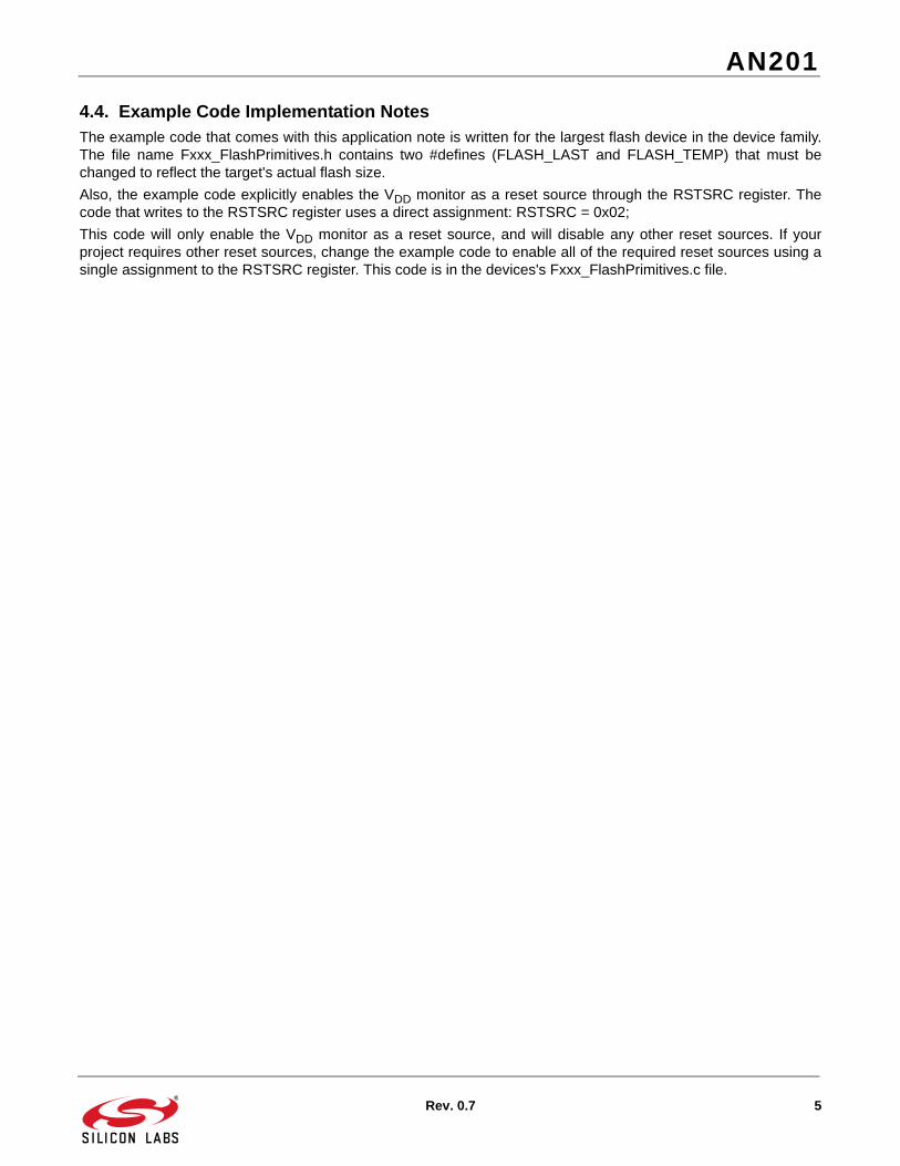
4.4. Example Code Implementation NotesThe example code that comes with this application note is written for the largest flash device in the device family.The file name Fxxx_FlashPrimitives.h contains two #defines (FLASH_LAST and FLASH_TEMP) that must bechanged to reflect the target's actual flash size.
Also, the example code explicitly enables the VDD monitor as a reset source through the RSTSRC register. Thecode that writes to the RSTSRC register uses a direct assignment: RSTSRC = 0x02;
This code will only enable the VDD monitor as a reset source, and will disable any other reset sources. If yourproject requires other reset sources, change the example code to enable all of the required reset sources using asingle assignment to the RSTSRC register. This code is in the devices's Fxxx_FlashPrimitives.c file.
Rev. 0.7 5

AN201
5. Advanced Flash OperationsThe basic routines described in Section 4 can be incorporated into more advanced routines that provide greaterflexibility. The following functions are commonly used flash routines that expand upon the basic routines. The codethat implements these routines for each device family is provided at the end of this application note in the filesnamed Fxxx_Utils.h and Fxxx_Utils.c.
Flash_Read—This routine reads multiple bytes from flash and returns a character string.
char * FLASH_Read (char *dest, FLADDR src, unsigned numbytes);
Flash_Write—This routine writes multiple bytes to flash. This function assumes that the target bytes have beencleared to 0xFF. If the bytes are not cleared to 0xFF, incorrect values might be stored in flash.
void FLASH_Write (FLADDR dest, char *src, unsigned numbytes);
Flash_Clear—This routines clears a string of bytes to 0xFF. The implementation of this function first copies thedata to temporary space, erases the page or pages, then copies the non-cleared bytes back to the original page orpages. This routine requires a spare page of flash to run, and it will clear up to one page size worth of data.
The FLASH_Clear routine can be used to clear bytes before they are written.
void FLASH_Clear (FLADDR addr, unsigned numbytes);
Flash_Update—This first clears the locations that are going to be written, and then writes the bytes. This routinerequires a spare page of flash to run, and it will update up to one page size worth of data.
The FLASH_Update routine combines FLASH_Clear and FLASH_Write into one routine.
FLASH_Update (FLADDR dest, char *src, unsigned numbytes);
Flash_Copy—This routine copies bytes from one location in flash to another location in flash. It assumes that thebytes are cleared to 0xFF. FLASH_Clear can be used to clear the bytes.
FLASH_Copy (FLADDR dest, FLADDR src, unsigned numbytes);
Flash_Fill—This routine fills bytes of flash with certain values. It assumes that bytes have been previously clearedto 0xFF.
void FLASH_Fill (FLADDR addr, ULONG length, UCHAR fill);
6 Rev. 0.7

AN201
6. Flash Write and Erase Guidelines
Any system which contains routines which write or erase flash memory from software involves some risk that thewrite or erase routines will execute unintentionally if the CPU is operating outside its specified operating range ofVDD, system clock frequency, or temperature. This accidental execution of flash modifying code can result in alter-ation of flash memory contents causing a system failure that is only recoverable by re-flashing the code in thedevice.
The following guidelines are recommended for any system which contains routines which write or erase flash fromcode.
6.1. VDD Maintenance and the VDD Monitor
1. If the system power supply is subject to voltage or current "spikes," add sufficient transient protection devices to the power supply to ensure that the supply voltages listed in the Absolute Maximum Ratings table are not exceeded.
2. If the device has a minimum VDD rise time specification, ensure that it is met. If the system cannot meet the rise time specification, then add an external VDD brownout circuit to the RST pin of the device that holds the device in reset until VDD reaches 2.7 V and re-asserts RST if VDD drops below 2.7 V.
3. Enable the on-chip VDD monitor and enable the VDD monitor as a reset source as early in code as possible. This should be the first set of instructions executed after the Reset Vector. For C-based systems, this will involve modifying the startup code added by the C compiler. See your compiler documentation for more details. Ensure that there are no delays in software between enabling the VDD monitor and enabling the VDD monitor as a reset source.
4. As an added precaution, explicitly enable the VDD monitor and enable the VDD monitor as a reset source inside the functions that write and erase flash memory. The VDD monitor enable instructions should be placed just after the instruction to set PSWE to a 1, but before the flash write or erase operation instruction.
5. Ensure that all writes to the RSTSRC (Reset Sources) register use direct assignment operators and explicitly DO NOT use the bit-wise operators (such as AND or OR). For example, "RSTSRC = 0x02" is correct. "RSTSRC |= 0x02" is incorrect.
6. Ensure that all writes to the RSTSRC register explicitly set the PORSF bit to a 1. Areas to check are initialization code which enables other reset sources, such as the Missing Clock Detector or Comparator, for example, and instructions which force a Software Reset. A global search on "RSTSRC" can quickly verify this.
7. If the device has a high and low threshold setting for the VDD monitor, enable the high setting.
Rev. 0.7 7

AN201
Table 1. VDD Monitor Enabling
Family How to enable the VDD monitor How to enable as a reset source
‘F00x (always enabled) (always enabled)
‘F01x (always enabled) (always enabled)
‘F02x Connect MONEN pin to VDD Enabled if MONEN pulled high
‘F04x Connect MONEN pin to VDD RSTSRC = 0x02;
‘F06x Connect MONEN pin to VDD RSTSRC = 0x02;
‘F12x, ‘F13x Connect MONEN pin to VDD RSTSRC = 0x02;
‘F2xx (always enabled on 48 pin package)Connect MONEN pin to VDD on 32 pin package
Enabled if MONEN pulled high
‘F30x (always enabled) RSTSRC = 0x02;1
‘F31x VDMEN = 1 RSTSRC = 0x02;2
‘F32x VDMEN = 1 RSTSRC = 0x02;2
‘F326 VDMEN = 1 RSTSRC = 0x02;2
‘F33x VDMEN = 1 RSTSRC = 0x02;2
‘F34x VDMEN = 1 RSTSRC = 0x02;2
‘F35x VDMEN = 1 RSTSRC = 0x02;2
‘F36x VDMEN = 1 RSTSRC = 0x02;2
‘F41x VDMEN = 1; VDMLVL = 1 RSTSRC = 0x02;2
'F50x, F51x VDMEN = 1; VDMLVL = 1 RSTSRC = 0x02;2
‘F52x, ‘F53x VDMEN = 1; VDMLVL = 1 RSTSRC = 0x02;2
‘F54x VDMEN = 1; VDMLVL = 1 RSTSRC = 0x02;2
'F55x, F56x, F57x VDMEN = 1; VDMLVL = 1 RSTSRC = 0x02;2
'F58x, F59x VDMEN = 1; VDMLVL = 1 RSTSRC = 0x02;2
‘F92x, F93x VDMEN = 1 RSTSRC = 0x02;2
‘F96x VDMEN = 1 RSTSRC = 0x02;2
‘F98x, F99x VDMEN = 1 RSTSRC = 0x02;2
Si100x VDMEN = 1 RSTSRC = 0x02;2
Si101x VDMEN = 1 RSTSRC = 0x02;2
Notes:1. On the ‘F30x devices, enabling the VDD monitor by setting the PORSF bit when the VDD monitor is disabled may cause
a system reset.2. In software which writes or erases flash memory, the VDD monitor should be enabled as a reset source immediately
following setting VDMEN to a 1.
8 Rev. 0.7

AN201
6.2. PSWE Maintenance1. Reduce the number of places in code where the PSWE bit (b0 in PSCTL) is set to a 1. There should be
exactly one routine in code that sets PSWE to a 1 to write flash bytes and one routine in code that sets PSWE and PSEE both to a 1 to erase flash pages.
2. Minimize the number of variable accesses while PSWE is set to a 1. Handle pointer address updates and loop variable maintenance outside the "PSWE = 1; ... PSWE = 0;" area.
3. Disable interrupts prior to setting PSWE to a 1 and leave them disabled until after PSWE has been reset to 0. Any interrupts posted during the flash write or erase operation will be serviced in priority order after the flash operation has been completed and interrupts have been re-enabled by software.
4. Ensure that the flash write and erase pointer variables are not located in XRAM. See your compiler documentation for instructions regarding how to explicitly locate variables in different memory areas.
5. Add address bounds checking to the routines that write or erase flash memory to ensure that a routine called with an illegal address does not result in modification of the flash.
6.3. System Clock1. If operating from an external crystal, be advised that crystal performance is susceptible to electrical
interference and is sensitive to layout and to changes in temperature. If the system is operating in an electrically noisy environment, use the internal oscillator or use an external CMOS clock.
2. If operating from the external oscillator, switch to the internal oscillator during flash write or erase operations. The external oscillator can continue to run, and the CPU can switch back to the external oscillator after the flash operation has completed.
Rev. 0.7 9

AN201
DOCUMENT CHANGE LIST
Revision 0.1 to Revision 0.2 Updated list of relevant devices.
Add all new content to "6. Flash Write and Erase Guidelines" on page 7.
Added example code for 'F340 devices.
Added example code for 'F326/7 devices.
Fixed example code for 'F320 devices.
Revision 0.2 to Revision 0.3 Added C8051F41x and C8051F52x-53x
documentation
Added clarification of the RSTSRC register in "4.4. Example Code Implementation Notes" on page 5.
Revision 0.3 to Revision 0.4 Added C8051F36x documentation.
Revision 0.4 to Revision 0.5 Added C8051F50x-51x and C8051F58x-59x
documentation.
Removed example code; it is still available as a separate download.
Revision 0.5 to Revision 0.6 Added C8051F54x, C8051F55x-56x-57x,
C8051F92x-93x, C8051F96x, C8051F98x-99x, Si100x, and Si101x documentation.
Revision 0.6 to Revision 0.7 Revised introduction and Contact information.
10 Rev. 0.7

http://www.silabs.com
Silicon Laboratories Inc.400 West Cesar ChavezAustin, TX 78701USA
Simplicity Studio
One-click access to MCU and wireless tools, documentation, software, source code libraries & more. Available for Windows, Mac and Linux!
IoT Portfoliowww.silabs.com/IoT
SW/HWwww.silabs.com/simplicity
Qualitywww.silabs.com/quality
Support and Communitycommunity.silabs.com
DisclaimerSilicon Labs intends to provide customers with the latest, accurate, and in-depth documentation of all peripherals and modules available for system and software implementers using or intending to use the Silicon Labs products. Characterization data, available modules and peripherals, memory sizes and memory addresses refer to each specific device, and "Typical" parameters provided can and do vary in different applications. Application examples described herein are for illustrative purposes only. Silicon Labs reserves the right to make changes without further notice and limitation to product information, specifications, and descriptions herein, and does not give warranties as to the accuracy or completeness of the included information. Silicon Labs shall have no liability for the consequences of use of the information supplied herein. This document does not imply or express copyright licenses granted hereunder to design or fabricate any integrated circuits. The products are not designed or authorized to be used within any Life Support System without the specific written consent of Silicon Labs. A "Life Support System" is any product or system intended to support or sustain life and/or health, which, if it fails, can be reasonably expected to result in significant personal injury or death. Silicon Labs products are not designed or authorized for military applications. Silicon Labs products shall under no circumstances be used in weapons of mass destruction including (but not limited to) nuclear, biological or chemical weapons, or missiles capable of delivering such weapons.
Trademark InformationSilicon Laboratories Inc.® , Silicon Laboratories®, Silicon Labs®, SiLabs® and the Silicon Labs logo®, Bluegiga®, Bluegiga Logo®, Clockbuilder®, CMEMS®, DSPLL®, EFM®, EFM32®, EFR, Ember®, Energy Micro, Energy Micro logo and combinations thereof, "the world’s most energy friendly microcontrollers", Ember®, EZLink®, EZRadio®, EZRadioPRO®, Gecko®, ISOmodem®, Precision32®, ProSLIC®, Simplicity Studio®, SiPHY®, Telegesis, the Telegesis Logo®, USBXpress® and others are trademarks or registered trademarks of Silicon Labs. ARM, CORTEX, Cortex-M3 and THUMB are trademarks or registered trademarks of ARM Holdings. Keil is a registered trademark of ARM Limited. All other products or brand names mentioned herein are trademarks of their respective holders.


![[My] Experiences building games in Visual Basic & Flash Focus on 'cannonball' Jeanine Meyer Math Senior Seminar](https://img.pdfslide.us/doc/110x75/5697bfd21a28abf838cab7b9/my-experiences-building-games-in-visual-basic-flash-focus-on-cannonball.jpg)