Embed Size (px)
Citation preview
Rigid-Flex PCB Right the First Time - Without Paper Dolls
Benjamin Jordan Altium Inc.
Abstract
The biggest problem with designing rigid-flex hybrid PCBs is making sure everything will fold in the right way, while maintaining good flex-circuit stability and lifespan. The next big problem to solve is the conveyance of the design to a fabricator who will clearly understand the design intent and therefore produce exactly what the designer/engineer intended. Rigid-Flex circuit boards require additional cutting and lamination stages, and more exotic materials in manufacturing and therefore the cost of re-spins and failures are very much higher than traditional rigid boards. To reduce the risk and costs associated with rigid-flex design and prototyping, it is desirable to model the flexible parts of the circuit in 3D CAD to ensure correct form and fit. In addition it is necessary to provide absolutely clear documentation for manufacturing to the fabrication and assembly houses.
The traditional attempt most design teams use to mitigate these risks is to create a "paper doll" of the PCB, by printing out a 1:1 representation of the board and then folding it up to fit a sample enclosure. This has a number of issues:
1) The paper doll does not also model the 3D thickness of the rigid and flex sections.2) The paper doll does not include 3D models of the electronic components mounted on the PCB.3) This approach requires a physical sample of the final enclosure which may not yet be final in it's design either.4) If the mechanical enclosure is custom designed, a costly 3D print will be required for testing. This adds much time
and expense to the project. As cool as 3D printers are, it's not a sensible use for them if the modeling can be doneentirely in software.
This paper discusses practical steps in two approaches to solve these problems, contrasting against the traditional "paper doll" approach above.
In the first scenario, a 3D MCAD model of the PCB assembly can be created in the MCAD package where a "sheet metal" model can be generated for the PCB substrate model. This sheet metal model can be bent into shape in the MCAD software to fit the final enclosure and check for clearance violations. This is not the best approach but it is better than paper dolls.
In the second scenario, a significant part of the enclosure or mechanical assembly model is brought from the MCAD package into the PCB design software, where the rigid-flex board outline can be designed specifically to fit with it. Rigid-flex layer stack sections can be defined and then flexible circuit areas have bending lines added. In the PCB design tool's 3D mode, the folds are then implemented to reveal where potential clearance violations and interference occurs. The PCB design can then be interactively modified to resolve the problems and check right away - without having to build any further mock-ups or translate design databases from one tool to another.
Introduction
Rigid-Flex can have many benefits, and many designers are at least considering it today that previously did not have to. More Printed Circuit Board (PCB) designers are facing higher pressures to build ever more densely populated electronics, and with that come additional pressures to reduce costs and time in manufacturing. Rigid-Flex PCB technology offers a solution that is viable for many product designs facing these challenges.
Yet there are aspects of rigid-flex technology, which could be potholes in the road for newcomers. So it’s wise to first understand how flex circuits and rigid-flex boards are actually made. There is however great difficulty in making sure everything will fold in the right way, while maintaining good flex-circuit stability and lifespan.
In addition, design hand-off to the fabricator is fraught with risk, especially for those less experienced (either in design or manufacture). First, there must be absolutely clear documentation around what is required. Such documentation includes layer stack and material definitions, fabrication drawings, and design notes. If these items are not accurate and complete there will be production delays at best, and scrap prototypes at worst. Second, the PCB layout and design is still traditionally carried out in 2D CAD systems where it is difficult to visualize or model how the components mounted on the final PCB
As originally published in the IPC APEX EXPO Conference Proceedings.
Assembly (PCBA) will fit in 3D space when the rigid-flex circuit is in operation. Third, problems with assembly of the folded flex circuit may not be discovered until boards are in pick-and-place (PNP) or during final prototype assembly into the target enclosure. These issues dramatically increase the risk and potential costs of developing a successful product around a rigid-flex PCB.
Rigid-Flex PCB Construction
To best understand the problems discussed in this paper it is necessary to offer a very brief overview of typical rigid-flex PCB construction. This subject matter is treated lightly here but a more thorough discussion can be found in the author’s guidebook: “Rigid-Flex PCB Design: A Guidebook for Designers”.[1]
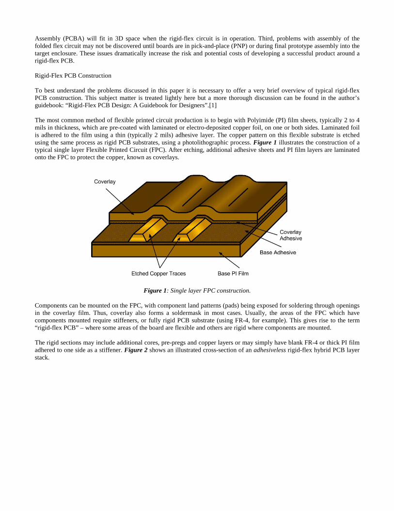
The most common method of flexible printed circuit production is to begin with Polyimide (PI) film sheets, typically 2 to 4 mils in thickness, which are pre-coated with laminated or electro-deposited copper foil, on one or both sides. Laminated foil is adhered to the film using a thin (typically 2 mils) adhesive layer. The copper pattern on this flexible substrate is etched using the same process as rigid PCB substrates, using a photolithographic process. Figure 1 illustrates the construction of a typical single layer Flexible Printed Circuit (FPC). After etching, additional adhesive sheets and PI film layers are laminated onto the FPC to protect the copper, known as coverlays.
Figure 1: Single layer FPC construction.
Components can be mounted on the FPC, with component land patterns (pads) being exposed for soldering through openings in the coverlay film. Thus, coverlay also forms a soldermask in most cases. Usually, the areas of the FPC which have components mounted require stiffeners, or fully rigid PCB substrate (using FR-4, for example). This gives rise to the term “rigid-flex PCB” – where some areas of the board are flexible and others are rigid where components are mounted.
The rigid sections may include additional cores, pre-pregs and copper layers or may simply have blank FR-4 or thick PI film adhered to one side as a stiffener. Figure 2 shows an illustrated cross-section of an adhesiveless rigid-flex hybrid PCB layer stack.
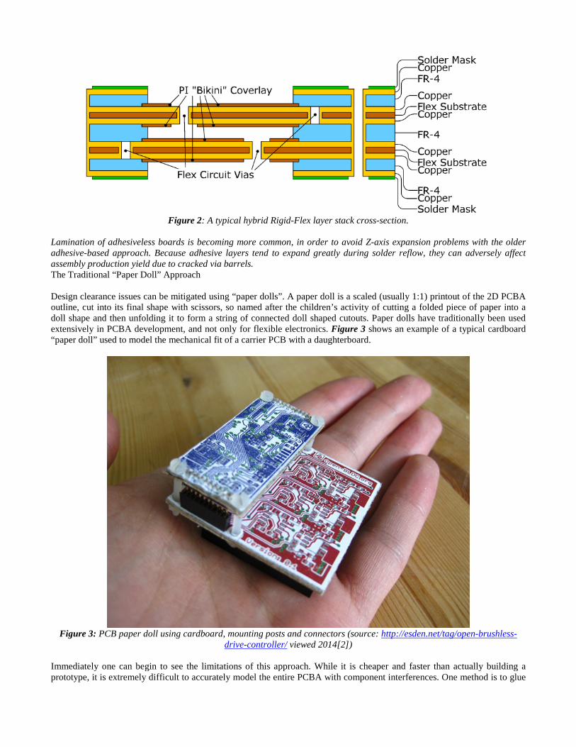
Figure 2: A typical hybrid Rigid-Flex layer stack cross-section.
Lamination of adhesiveless boards is becoming more common, in order to avoid Z-axis expansion problems with the older adhesive-based approach. Because adhesive layers tend to expand greatly during solder reflow, they can adversely affect assembly production yield due to cracked via barrels. The Traditional “Paper Doll” Approach
Design clearance issues can be mitigated using “paper dolls”. A paper doll is a scaled (usually 1:1) printout of the 2D PCBA outline, cut into its final shape with scissors, so named after the children’s activity of cutting a folded piece of paper into a doll shape and then unfolding it to form a string of connected doll shaped cutouts. Paper dolls have traditionally been used extensively in PCBA development, and not only for flexible electronics. Figure 3 shows an example of a typical cardboard “paper doll” used to model the mechanical fit of a carrier PCB with a daughterboard.
Figure 3: PCB paper doll using cardboard, mounting posts and connectors (source: http://esden.net/tag/open-brushless-drive-controller/ viewed 2014[2])
Immediately one can begin to see the limitations of this approach. While it is cheaper and faster than actually building a prototype, it is extremely difficult to accurately model the entire PCBA with component interferences. One method is to glue
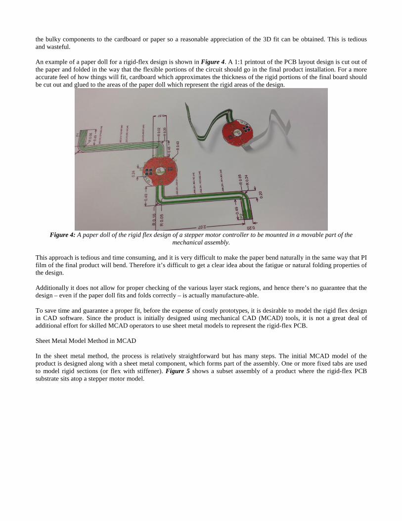
the bulky components to the cardboard or paper so a reasonable appreciation of the 3D fit can be obtained. This is tedious and wasteful. An example of a paper doll for a rigid-flex design is shown in Figure 4. A 1:1 printout of the PCB layout design is cut out of the paper and folded in the way that the flexible portions of the circuit should go in the final product installation. For a more accurate feel of how things will fit, cardboard which approximates the thickness of the rigid portions of the final board should be cut out and glued to the areas of the paper doll which represent the rigid areas of the design.
Figure 4: A paper doll of the rigid flex design of a stepper motor controller to be mounted in a movable part of the
mechanical assembly. This approach is tedious and time consuming, and it is very difficult to make the paper bend naturally in the same way that PI film of the final product will bend. Therefore it’s difficult to get a clear idea about the fatigue or natural folding properties of the design. Additionally it does not allow for proper checking of the various layer stack regions, and hence there’s no guarantee that the design – even if the paper doll fits and folds correctly – is actually manufacture-able. To save time and guarantee a proper fit, before the expense of costly prototypes, it is desirable to model the rigid flex design in CAD software. Since the product is initially designed using mechanical CAD (MCAD) tools, it is not a great deal of additional effort for skilled MCAD operators to use sheet metal models to represent the rigid-flex PCB. Sheet Metal Model Method in MCAD In the sheet metal method, the process is relatively straightforward but has many steps. The initial MCAD model of the product is designed along with a sheet metal component, which forms part of the assembly. One or more fixed tabs are used to model rigid sections (or flex with stiffener). Figure 5 shows a subset assembly of a product where the rigid-flex PCB substrate sits atop a stepper motor model.

Figure 5: Stepper motor model and rigid-flex
This is a nice clean way of discovering what area is available for the PCB substrate, but it is still necessary to get this shape into the PCB editor’s workspace. Generally, MCAD software packages that model sheet metal have an “unbend” or “unfold” feature which is usually used for generating the sheet metal stamping outputs needed for sheet metal fabrication. In this case however we need to generate a model suitable for import into the PCB editor. The unfolded sheet metal model of the board is shown in Figure 6 and areas subject to bending are highlighted, which can assist in planning for component placement regions known as “rooms” later on. This sheet metal model can be exported to the PCB design software (ECAD) as either IDF or DXF in its simplest form. The PCB editor imports this board shape or outline from which the PCB shape is actually created. Components are placed in the PCB editor and then an IDF file is generated to transmit the PCB shape and component locations back to the MCAD database, where the mechanical designer can re-fold the board substrate. However in most cases this is an unwieldy task, with some manual effort involved in maintaining the placement associations of the components on the rigid board sections in their folded positions.
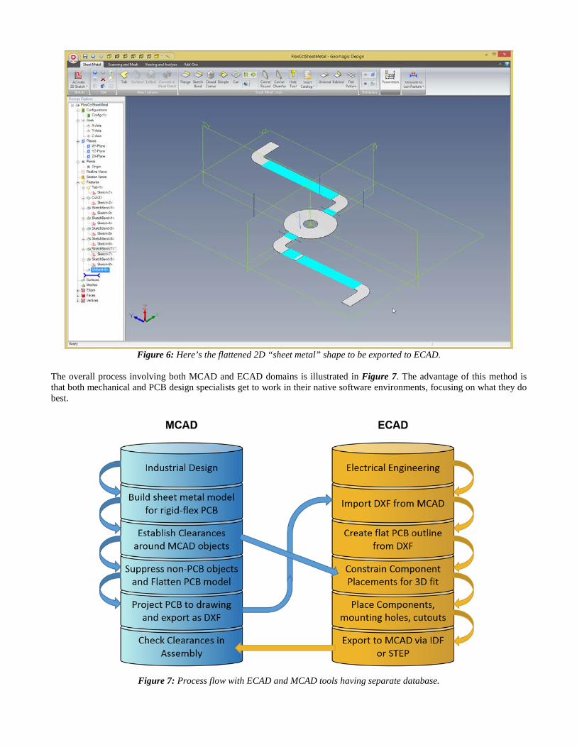
Figure 6: Here’s the flattened 2D “sheet metal” shape to be exported to ECAD.
The overall process involving both MCAD and ECAD domains is illustrated in Figure 7. The advantage of this method is that both mechanical and PCB design specialists get to work in their native software environments, focusing on what they do best.
Figure 7: Process flow with ECAD and MCAD tools having separate database.
Direct ECAD 3D Model
As the name suggests, in this new method the PCB layout design, Rigid-Flex folding design, and mechanical assembly are all modeled together directly within the ECAD software. Advancements in most modern PCB design tools enable proper 3D visualization at a minimum, supported largely by the use of 3D STEP models of the components and mechanical enclosure or parts thereof.
ECAD software with 3D functionality is not intended to replace dedicated mechanical CAD systems. At least, not until engineering affords such a multi-disciplinary approach. Meanwhile, it is a major step forward in terms of improved workflow, and reduced waste of time and materials. High-end PCB design tools allow for Native 3D PCB design: this includes not only 3D visualization of the PCBA, but also full 3D modeling of the PCB including dielectrics and copper. Such 3D models can also be exported for thorough thermal and electromagnetic investigations.
With additional tools for Native 3D modeling of the board materials, components, and mechanical object such as the enclosure, proper clearance checking and animation of flexible circuit elements is possible, offering some guarantee that the final rigid-flex design will fit in the designed enclosure and function according to specifications.
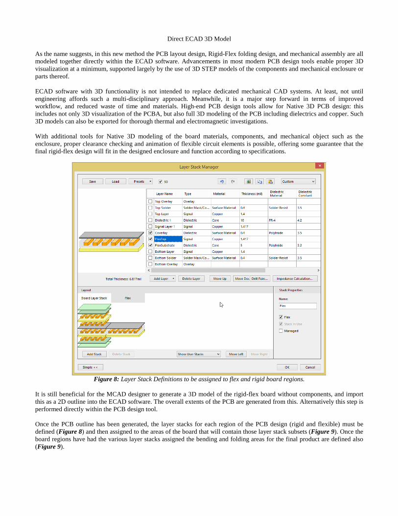
Figure 8: Layer Stack Definitions to be assigned to flex and rigid board regions.
It is still beneficial for the MCAD designer to generate a 3D model of the rigid-flex board without components, and import this as a 2D outline into the ECAD software. The overall extents of the PCB are generated from this. Alternatively this step is performed directly within the PCB design tool.
Once the PCB outline has been generated, the layer stacks for each region of the PCB design (rigid and flexible) must be defined (Figure 8) and then assigned to the areas of the board that will contain those layer stack subsets (Figure 9). Once the board regions have had the various layer stacks assigned the bending and folding areas for the final product are defined also (Figure 9).
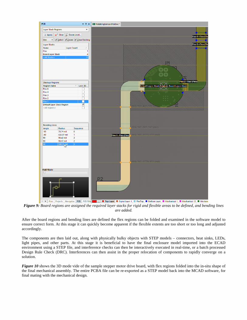
Figure 9: Board regions are assigned the required layer stacks for rigid and flexible areas to be defined, and bending lines are added.
After the board regions and bending lines are defined the flex regions can be folded and examined in the software model to ensure correct form. At this stage it can quickly become apparent if the flexible extents are too short or too long and adjusted accordingly.
The components are then laid out, along with physically bulky objects with STEP models – connectors, heat sinks, LEDs, light pipes, and other parts. At this stage it is beneficial to have the final enclosure model imported into the ECAD environment using a STEP file, and interference checks can then be interactively executed in real-time, or a batch processed Design Rule Check (DRC). Interferences can then assist in the proper relocation of components to rapidly converge on a solution.
Figure 10 shows the 3D mode vide of the sample stepper motor drive board, with flex regions folded into the in-situ shape of the final mechanical assembly. The entire PCBA file can be re-exported as a STEP model back into the MCAD software, for final mating with the mechanical design.
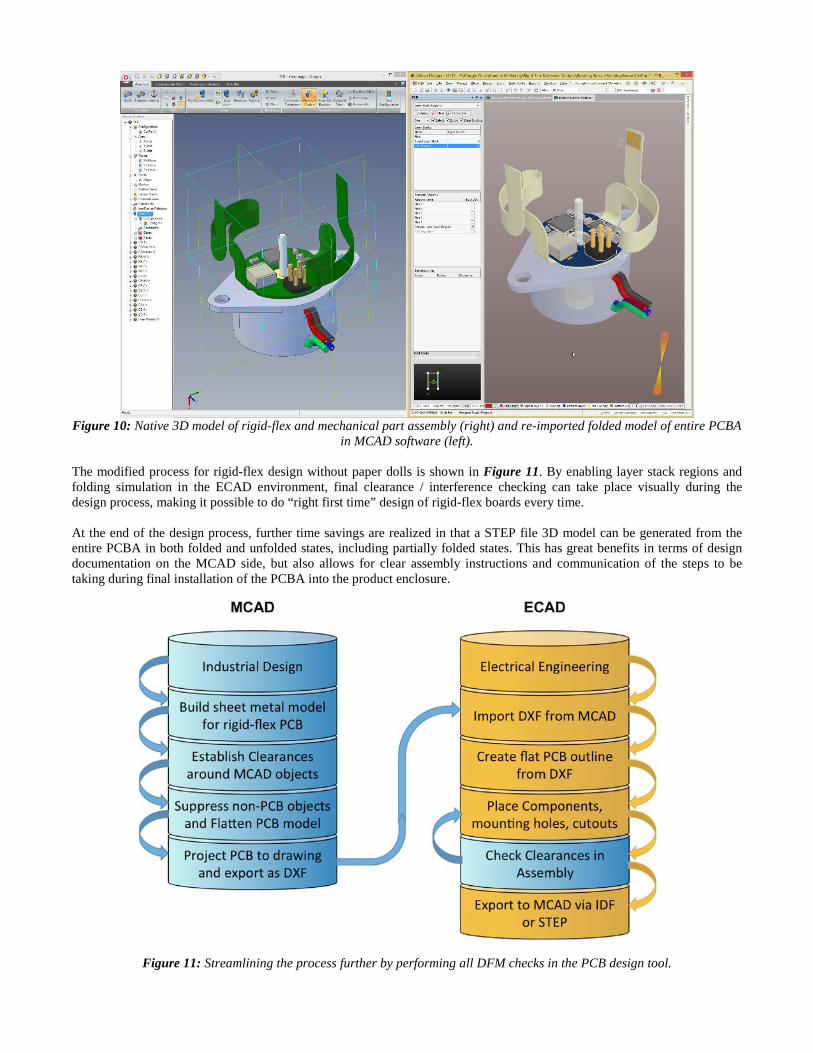
Figure 10: Native 3D model of rigid-flex and mechanical part assembly (right) and re-imported folded model of entire PCBA in MCAD software (left).
The modified process for rigid-flex design without paper dolls is shown in Figure 11. By enabling layer stack regions and folding simulation in the ECAD environment, final clearance / interference checking can take place visually during the design process, making it possible to do “right first time” design of rigid-flex boards every time.
At the end of the design process, further time savings are realized in that a STEP file 3D model can be generated from the entire PCBA in both folded and unfolded states, including partially folded states. This has great benefits in terms of design documentation on the MCAD side, but also allows for clear assembly instructions and communication of the steps to be taking during final installation of the PCBA into the product enclosure.
Figure 11: Streamlining the process further by performing all DFM checks in the PCB design tool.

Using this new integrated method, at least 50% of the time normally taken to verify and validate PCB shape and folds can be saved, due to the interactive and instantaneous feedback nature of the approach.
Further time and error is reduced for final assembly, as clear images and video can be generated from the folding steps of the rigid-flex PCBA to discover the optimal assembly sequence. This video or image output can be utilized in both assembly and product service documentation.
A. Reference Material
1. Jordan, B 2013, Rigid-Flex PCB Design –A guidebook for designers, Altium Inc., La Jolla, CA.
2. Esden, 2009, The twisted world of Esden (Blog), viewed 13 October 2014, <http://esden.net/tag/open-brushless-drive-controller/>
3. Coombs, CF 2008, Printed Circuits Handbook, 6th edn, McGraw-Hill, New York, NY.
2. IPC 2011, Sectional Design Standard for Flexible Printed Boards, IPC-2223C, IPC, Bannockburn, Illinois.
3. Thermal Conductivity Polyimide Film 2013, Shinmax Technology Ltd., Taiwan, viewed 25 October 2013,<http://shinmax.taiwantrade.com.tw/products-detail/en_US/542706/Thermal_Conductivity_Polyimide_Film>.
4. TCM125-OE, Zhuhai Smartech Electronics & Machinery, China, viewed 25 October 2013,<http://www.vcdpickup.com/thomson.files/TCM125-OE.jpg>.
5. Machined Class A Die Coverlay 2011, GC Aero Inc., United States, viewed 25 October 2013, <http://gcaero.com/wp-content/uploads/2011/11/Punched-Coverfilm.jpg>.
6. Fine Blanking Die SKD11 / Din1.2379 For Flex Printed Circuit Board 2013, Haoji Stamping Tool & Die Co.,Ltd., China,viewed 31 October 2013, <http://www.metal-stampingdie.com/china-fine_blanking_die_skd11_din1_2379_for_flex_printed_circuit_board-1262774.html>
7. 1.6mm Immersion Gold FR4 & PI 6 Layer Rigid Flexible Board / Multilayer Printed Circuit Board 2013, YYUXINGShenzhen Electronics Co., LTD., Korea, viewed 25 October 2013, <http://www.china-pcbmanufacturer.com/photo/pl425064-fr4_pi_6_layer_immersion_4_4mgold_flexible_printed_circuit_board_assembly_for_led.jpg>.