Embed Size (px)
Citation preview
Research Collection
Doctoral Thesis
VLSI Design, Optimization, and Implementation of ChannelDecoding in Wireless Systems
Author(s): Roth, Christoph
Publication Date: 2015
Permanent Link: https://doi.org/10.3929/ethz-a-010497725
Rights / License: In Copyright - Non-Commercial Use Permitted
This page was generated automatically upon download from the ETH Zurich Research Collection. For moreinformation please consult the Terms of use.
ETH Library
VLSI Design, Optimization, and Implementation ofChannel Decoding in Wireless Systems

DISS. ETH NO. 22672
VLSI Design, Optimization,and Implementation ofChannel Decoding in
Wireless Systems
A thesis submitted to attain the degree of
DOCTOR OF SCIENCES of ETH ZURICH
(Dr. sc. ETH Zurich)
presented by
CHRISTOPH ROTHMSc ETH EEIT
born on 28.06.1984citizen of Zurich ZH and Hemberg SG
accepted on the recommendation of
Prof. Dr. Qiuting Huang, examinerProf. Dr. Andreas Burg, co-examiner
2015

Acknowledgments
First of all, I would like to express my sincere gratitude to Prof. Dr.Qiuting Huang for stepping in as thesis advisor, for his support andinterest in my work, and for giving me the opportunity to work onvery interesting projects at the intersection of academia and industry.I am also very grateful to Prof. Dr. Andy Burg who kindly agreed toact as co-examiner for my thesis. I have always highly appreciatedand enjoyed his helpful research inputs, his concise and constructivecriticism, and the interesting collaborations we had since I performedmy industry internship under his guidance back in 2008.
I am deeply thankful to Dr. Christian Benkeser and Prof. Dr.Christoph Studer. Christoph sparked my enthusiasm for wireless com-munications and digital VLSI circuit design when he was supervisingmy semester project at the Integrated Systems Laboratory (IIS) in2007 and later taught me a lot about conducting research and writingpapers. Christian, who performed his postdoctoral studies in Prof.Dr. Huang’s group for more than two years, was a continuous sourceof advice and constructive ideas, and with his constant support heinvaluably contributed to the success of my thesis.
Special thanks go to the digital part of the analog mixed-signaldesign group at IIS, in particular to Sandro Belfanti for the fruitfulcollaboration on turbo decoding and to Stefan Altorfer-Zwicky, KarimBadawi, Harald Kroll, and Benjamin Weber for the many interestingdiscussions and sparkling conversations that usually revolved aboutmany topics far beyond the scope of our research. I would alsolike to thank my former colleagues Dr. Pascal Meinerzhagen andDr. Alessandro Cevrero for our joint projects on LDPC decoding.Furthermore, I would like to thank present and former colleagues
v
vi
of the analog mixed-signal design and the digital circuits and sys-tems groups at IIS for their friendship and for providing such anenjoyable workplace atmosphere, in particular David Bellasi, LucaBettini, Rene Blattman, Schekeb Fateh, Michael Gautschi, ChristophKeller, Michael Muhlberghuber, Michael Schaffner, Philipp Schonle,Benjamin Sporrer, Dr. Jurg Treichler, and Pirmin Vogel.
Moreover, I am most grateful to all staff members of IIS, espe-cially to Dr. Thomas Burger, to Dr. Norbert Felber and Prof. Dr.Hubert Kaeslin for their continuous efforts in introducing studentsinto the exciting field of VLSI, and to Dr. Frank Gurkaynak and BeatMuheim from the Microelectronics Design Center for providing suchan excellent electronic design flow.
I highly appreciate the contributions by all students who per-formed a semester project or master’s thesis under my supervision. Iam especially thankful to Felix Arnold, Gabriel Grani, Michael Jakob,Kristoffer Nordstrom, Daniel Riegger, Adrian Schoch, David Sommer,and Daniel Stadelmann for their work on the VLSI design of Viterbi,SOVA, and turbo decoding.
From a personal standpoint I wish to thank my close family mem-bers for all their encouragement and enduring non-technical supportduring all these years. I am especially grateful to my father for caringso much about my education and making my studies at ETH Zurichpossible. I am going to miss our weekly lunch dates at the ETHcafeteria.
Finally, I would like to dedicate this thesis to my beloved wifeLeyla. Without her unlimited patience and understanding for mywork, her caring support, and her unconditional love I could neverhave succeeded in this endeavor. Thank you!
Abstract
Today’s mobile information society has a steady demand for ever-increasing data rates and better quality-of-service in wireless systems.To meet this demand standards organizations involved with the wire-less industry are increasingly relying on modern high-performancechannel codes such as low-density parity-check (LDPC) and turbocodes. These forward error-correction codes achieve near-optimal per-formance and thus enable highly robust wireless information transfer.
Unfortunately, the excellent error-correction capabilities of LDPCcodes and turbo codes come at the expense of substantial computa-tional complexity in mobile receivers as the decoding of these codesis based on sophisticated iterative algorithms. In addition, practicaldecoder implementations must usually support a wide range of opera-tion modes in order to enable the wireless system to adapt to varioustransmission environments. This combination of high computationalrequirements and high flexibility demands renders the implementationof LDPC and turbo decoders for wireless systems a considerable re-search challenge. During the last decade, significant progress has beenmade in the development of low-complexity LDPC and turbo decodingalgorithms and the implementation of these algorithms in flexiblededicated very-large-scale integration (VLSI) circuits. Nevertheless,the implementation complexity of LDPC and turbo decoders remainshigh. Typically, these decoders are found among the most area andpower intensive components in wireless baseband receivers and thussignificantly strain the tight cost and power budgets of mobile battery-powered devices.
Hence, the main part of this thesis is concerned with reducingthe high VLSI implementation costs associated with LDPC and turbo
vii
viii ABSTRACT
decoders. In particular, we provide concepts and solutions that enablecost- and power-efficient dedicated VLSI implementations which arein line with the high throughput and flexibility requirements of mod-ern and next-generation wireless standards. To this end, we explorenovel decoder design approaches and consider careful optimization ofexisting approaches on algorithm, architecture, and circuit level. Sev-eral reference decoder application-specific integrated circuit (ASIC)implementations tailored to a selection of relevant wireless standardsare described, proving the applicability and efficacy of the proposedtechniques.
Channel decoders in mobile receivers are usually embedded ina sophisticated channel decoding chain, which provides additionalfunctionality to increase the robustness of transmission. In modernand future wireless systems, such channel decoding chains must betunable for a vast number of transmission modes and support ad-vanced features such as the hybrid automatic repeat request (hybrid-ARQ) protocol. These requirements have a significant impact onoverall receiver implementation complexity. Hence, in the second partof this thesis, we assess the VLSI implementation challenges associatedwith channel decoding chains for wireless systems. To this end, wedevelop a dedicated channel decoding chain VLSI architecture focus-ing on a representative enhanced 3G cellular standard. The proposedarchitecture has been implemented as part of a complete basebandreceiver ASIC with strong emphasis on area and power efficiency.The corresponding implementation results provide reference for thetrue VLSI implementation complexity of channel decoding in wirelesssystems.
Zusammenfassung
Die heutige mobile Informationsgesellschaft stellt immer hohere An-spruche an drahtlose Kommunikationssysteme in Bezug auf Datenrateund Ubertragungsqualitat. Um diesen Anspruchen gerecht zu werden,setzen neuere drahtlose Ubertragungsstandards vermehrt auf moderneleistungsstarke Fehlerkorrekturcodes wie LDPC (low-density parity-check)-Codes und Turbo-Codes. Diese zwei Arten von Kanalcodes bie-ten eine herausragende Fehlerkorrektur nahe der theoretischen Grenzeund ermoglichen so eine hochst robuste drahtlose digitale Informati-onsubertragung.
Leider ist die starke Fehlerkorrektur von LDPC- und Turbo-Codesmit einem erheblichen Rechenaufwand auf Empfangerseite verbunden,da die Decodierverfahren fur diese Codes auf ressourcenintensiveniterativen Algorithmen beruhen. Gleichzeitig mussen Implementie-rungen von LDPC- und Turbo-Decodern in der Praxis sehr flexibelsein und eine breite Palette an verschiedenen Ubertragungsmodi un-terstutzen. Diese Kombination von hohem Rechenaufwand und hohenFlexibilitatsanspruchen stellt eine besondere Herausforderung fur dieForschung dar. In den letzten Jahren konnten wichtige Fortschrittesowohl in der Entwicklung von Decodieralgorithmen mit reduzierterKomplexitat als auch in der Realisierung dieser Algorithmen als de-dizierte hochintegrierte (VLSI) Schaltungen erzielt werden. Trotzdemist die Komplexitat von heutigen LDPC- und Turbo-Decodern nochimmer sehr gross, und typischerweise zahlen diese Decoder zu denflachen- und leistungsintensivsten Komponenten in drahtlosen Basis-bandempfangern.
Daher liegt das Hauptaugenmerk dieser Arbeit auf der Reduk-tion der hohen VLSI Implementierungskomplexitat von LDPC- und
ix
x ZUSAMMENFASSUNG
Turbo-Decodern. Es werden Konzepte und Losungen prasentiert, dieeine kosteneffiziente Implementierung solcher Decoder ermoglichenund die im Einklang mit den hohen Datenraten und starken Flexibi-litatsanspruchen von modernen und zukunftigen drahtlosen Ubertra-gungsstandards stehen. Die vorgeschlagenen Konzepte und Losungenberuhen auf neuen Implementierungsansatzen und auf sorgfaltiger Op-timierung existierender Ansatze auf Algorithmus-, Architektur-, undSchaltungsebene. Die Machbarkeit und Effektivitat unserer Beitragewerden durch mehrere applikationspezifische integrierte Schaltungen(ASICs) von LDPC- und Turbo-Decodern fur eine Reihe von praxis-relevanten Ubertragungsstandards demonstriert.
LDPC- und Turbo-Decoder in mobilen Empfangern sind norma-lerweise eingebettet in einer ganzen Decodierkette, welche zusatzlicheMittel bietet, um die Qualitat der Informationsubertragung zu stei-gern. Mit den wachsenden Anforderungen an moderne und zukunftigeKommunikationssysteme mussen diese Decodierketten immer mehrFunktionen unterstutzen und werden so immer komplexer. Der zweiteTeil dieser Arbeit untersucht daher die VLSI Implementierungsher-ausforderungen, die mit solchen Decodierketten verbunden sind. Zudiesem Zweck wurde eine dedizierte VLSI Architektur fur die De-codierkette eines reprasentativen 3G Mobilfunkstandards entwickelt,und die vorgeschlagene Architektur wurde als Teil eines komplet-ten 3G Basisbandempfanger-ASICs mit Schwerpunkt auf Flachen-und Leistungseffizienz implementiert. Die Implementierungsresultategeben schlussendlich Auskunft uber den wahren Schaltungsaufwandsolcher Decodierketten.
Contents
Abstract vii
Zusammenfassung ix
1 Introduction 11.1 Modern Channel Coding . . . . . . . . . . . . . . . . . 2
1.1.1 LDPC Codes, Turbo Codes, and IterativeDecoding . . . . . . . . . . . . . . . . . . . . . 3
1.1.2 VLSI Integration Challenges . . . . . . . . . . 51.2 Thesis Contributions . . . . . . . . . . . . . . . . . . . 81.3 Thesis Outline . . . . . . . . . . . . . . . . . . . . . . 12
2 Preliminaries 132.1 System Model . . . . . . . . . . . . . . . . . . . . . . . 132.2 Low-Density Parity-Check Codes . . . . . . . . . . . . 17
2.2.1 Quasi-Cyclic LDPC Codes . . . . . . . . . . . . 192.2.2 Decoding of LDPC Codes . . . . . . . . . . . . 20
2.3 Turbo Codes . . . . . . . . . . . . . . . . . . . . . . . 272.3.1 Encoding of Turbo Codes . . . . . . . . . . . . 272.3.2 Decoding of Turbo Codes . . . . . . . . . . . . 292.3.3 The BCJR Algorithm . . . . . . . . . . . . . . 322.3.4 The Soft-Output Viterbi Algorithm . . . . . . 362.3.5 Error-Rate Performance Comparison . . . . . . 39
2.4 Summary . . . . . . . . . . . . . . . . . . . . . . . . . 40
xi
xii CONTENTS
3 VLSI Implementation of LDPC Decoding 433.1 High-Level Architecture Exploration . . . . . . . . . . 43
3.1.1 Full-Parallel Architecture . . . . . . . . . . . . 473.1.2 Row-Parallel Architecture . . . . . . . . . . . . 483.1.3 Block-Parallel Architecture . . . . . . . . . . . 493.1.4 Conclusions . . . . . . . . . . . . . . . . . . . . 51
3.2 Flexible QC-LDPC DecoderArchitecture . . . . . . . . . . . . . . . . . . . . . . . . 523.2.1 Architecture Overview . . . . . . . . . . . . . . 523.2.2 Node Computation Unit . . . . . . . . . . . . . 543.2.3 Cyclic Shifter Unit . . . . . . . . . . . . . . . . 573.2.4 Configurable Control Unit . . . . . . . . . . . . 583.2.5 Memory Requirements . . . . . . . . . . . . . . 59
3.3 Low-Power Memory Architecture . . . . . . . . . . . . 613.3.1 SRAM Macrocells versus SCMs . . . . . . . . . 613.3.2 SCM based Memory Architecture . . . . . . . . 62
3.4 Implementation Results . . . . . . . . . . . . . . . . . 643.4.1 QC-LDPC Decoder for WLAN with
Commercial SCMs . . . . . . . . . . . . . . . . 663.4.2 QC-LDPC Decoder for WLAN with
Custom Refresh-Free D-SCMs . . . . . . . . . . 69
4 VLSI Implementation of Turbo Decoding 734.1 High-Level Architecture Exploration . . . . . . . . . . 74
4.1.1 Serial Architecture . . . . . . . . . . . . . . . . 744.1.2 Subblock-Parallel Architecture . . . . . . . . . 764.1.3 Throughput of Turbo Decoders . . . . . . . . . 774.1.4 Summary . . . . . . . . . . . . . . . . . . . . . 79
4.2 SISO Decoder Architectures . . . . . . . . . . . . . . . 794.2.1 Sliding-Window BCJR Architecture . . . . . . 804.2.2 Improved-SOVA Architecture . . . . . . . . . . 884.2.3 Error-Rate Performance Comparison of
Sliding-Window Turbo Decoders . . . . . . . . 934.3 Design of Serial Turbo Decoders . . . . . . . . . . . . 96
4.3.1 Qualitative Architecture Comparison . . . . . . 964.3.2 VLSI Implementation Results for UMTS . . . . 1004.3.3 VLSI Implementation Results for E-EDGE . . 105
CONTENTS xiii
4.4 Design of Subblock-ParallelTurbo Decoders . . . . . . . . . . . . . . . . . . . . . . 1124.4.1 Constrained Throughput Evaluation . . . . . . 1134.4.2 Throughput Evaluation Example . . . . . . . . 1154.4.3 Alleviating the Parallel Turbo-Decoder
Predicament . . . . . . . . . . . . . . . . . . . 1194.4.4 VLSI Implementation Trade-off Analysis . . . . 124
5 Channel Decoding Chain Design for UMTS 1295.1 Overview on TD-SCDMA Evolutions . . . . . . . . . . 130
5.1.1 Legacy Channel Coding Chain . . . . . . . . . 1315.1.2 Enhanced Channel Coding Chain . . . . . . . . 134
5.2 VLSI Baseband Receiver Architecture . . . . . . . . . 1365.2.1 Channel Decoding Chain Architecture . . . . . 1385.2.2 Complete Channel Decoding Solution . . . . . 1415.2.3 Channel Decoding Chain Performance . . . . . 148
5.3 VLSI Implementation Results . . . . . . . . . . . . . . 1505.3.1 ASIC Overview . . . . . . . . . . . . . . . . . . 1515.3.2 Results and Discussion . . . . . . . . . . . . . . 152
6 Summary and Conclusion 157
Acronyms 165
Bibliography 169
Curriculum Vitae 181

Chapter 1
Introduction
During the last two decades, digital wireless communication has grownwith an astonishing pace from a niche application market to a globalmulti-billion dollar mass market. In 2002 — only eleven years afterthe first commercial GSM phone call — the worldwide number ofcell phone subscriptions surpassed the number of fixed phone sub-scriptions. At the end of 2014, the estimated number of global cellphone subscriptions reached 6.9 billion, which corresponds to 96%of the world population [1]. The foundation of this unprecedentedeconomic and technological success story is the strong interplay ofgroundbreaking advances in semiconductor technology, digital/analogintegrated circuit design, and communication theory combined withlong-term global standardization efforts. With the increasing prolif-eration of affordable portable computers, smart phones, and othermobile devices, the focus of the wireless industry has moved awayfrom voice-centric services towards data-centric services. As a con-sequence, data rates in wireless systems have increased dramaticallyin recent years, following an exponential growth that is in nice ac-cordance with Edholm’s Law [2], which states that data rates inwireless systems double roughly every 18 months. Projecting forward,Edholm’s Law indicates that the capabilities of wireless systems inthe near future will enable data rates of multiple gigabits per sec-ond and eventually converge with the capabilities of wired systems.In order to support the need for ever-increasing data rate, new air
1
2 CHAPTER 1. INTRODUCTION
interfaces are constantly under development, aiming at improvingspectral efficiency (e.g., through the specification of large modula-tion orders or multiple-input multiple-output (MIMO) transmissionschemes), while achieving better quality-of-service (QoS) and servinga larger number of users compared to previous standards. For in-stance, the LTE cellular standard specified by the third-generationpartnership project (3GPP) consortium is currently being deployedaround the world enabling a potential peak data rate of 300 Mbps,which corresponds to a 20× improvement compared to the widespreadHSPA enhancement of UMTS. At the same time, the evolved versionLTE-Advanced (LTE-A) has already been specified and promises tofurther augment peak data rates in cellular systems up to the 3 Gbpsmilestone. The well-established WLAN standard family has evolvedat a similar pace with its latest version IEEE 802.11ad waiting in thewings to boost peak data rate up to 7 Gbps.
The employment of strong channel coding is key to enable thehigh-throughput and stringent QoS requirements of modern and next-generation wireless standards to be met in practice. For this reason,wireless systems are increasingly relying on high-performance low-density parity-check (LDPC) and turbo codes. These modern forwarderror-correction codes are among the best-performing codes knowntoday and are able to improve the reliability of wireless transmissionsubstantially compared to classical block and convolutional codes.
1.1 Modern Channel CodingChannel coding is a core technology in any modern digital communica-tion system. It enables robust transmission of information under theinevitable signal distortions induced by the communication channel1while keeping the transmitted power low. This is realized via the useof a channel encoder on transmit side introducing a well-defined re-dundant structure to the transmitted messages, and a channel decoderon receive side exploiting this structure to correct the occurred trans-mission errors. The reliability of the overall communication system
1In wireless systems, the receive signal is typically distorted by thermal noise,fading caused by multi-path propagation, and interference from other wirelessservices.
1.1. MODERN CHANNEL CODING 3
heavily depends on the capabilities of the employed channel code andthe performance of the implemented channel decoding algorithm.
In order to increase the robustness of transmission further, wirelessstandards typically specify bit-interleaved coded modulation (BICM)schemes [3]. Accordingly, channel codes in wireless systems are usuallyembedded in a sophisticated channel coding chain that consists of oneor multiple interleaver stages, stream multiplexers, and other bit-leveloperations.
1.1.1 LDPC Codes, Turbo Codes, and IterativeDecoding
LDPC codes were proposed already by Gallager in his PhD thesis [4]in 1962. However, at that time — only four years after Kilby’sgroundbreaking invention of the integrated circuit — LDPC codeswere considered too complex for practical implementation and re-mained obscure for three decades. In the mean time, highly structuredalgebraic block and convolutional codes [5] were the dominating choicefor forward error-correction. With the invention of the famous Viterbialgorithm [6] in 1967, optimal decoding of convolutional codes becamefeasible, resulting in a widespread deployment of these codes. Despitetheir tremendous practical impact, however, these codes could by farnot achieve the information-theoretical limits anticipated by Shan-non’s fundamental noisy channel coding theorem set down in 1948.
The introduction of turbo codes in 1993 by Berrou et al. [7] and thesubsequent rediscovery of Gallager’s LDPC codes by MacKay et al.[8] in 1995 marked a breakthrough in coding theory and led to afundamental paradigm shift in this field of research, sparking theera of modern channel codes. Compared to classical channel codes,modern channel codes involve little algebra, but are understood ascomplex systems defined on sparse random graphical models whereboth encoding and decoding are accomplished by efficient local algo-rithms [9]. The seemingly random construction of modern channelcodes is in line with Shannon’s random coding argument and enablesperformance very close to the Shannon limit. It was soon realizedthat modern channel codes, including LDPC and turbo codes, can bedescribed in a generalized view using the framework of factor graphs,and that the decoding algorithms for these codes are in fact specific
4 CHAPTER 1. INTRODUCTION
instances of one single algorithm, which operates by iterative message-passing along the edges of the graph [10–12]. Although iterativemessage-passing is in general a sub-optimal decoding algorithm, itdelivers near-optimal performance for LDPC codes and turbo codeswith manageable complexity [11].
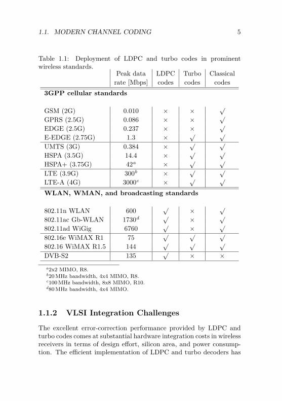
With the increasing capabilities of integrated circuits, both LDPCcodes and turbo codes have gradually been considered in various prac-tical applications. Table 1.1 summarizes the proliferation of LDPCand turbo codes in practical communication systems with a focus onprominent recent and emerging wireless standards.2 Since the use ofturbo codes was specified for UMTS in 1999, turbo codes have becomethe dominating choice for forward error-correction in enhanced-2G,3G, and emerging 4G cellular standards. The practical considerationof LDPC codes lagged somewhat behind the application of turbocodes. After the rediscovery of LDPC codes, researchers focused onfinding efficient structured codes that would simplify the encodingand decoding process while maintaining excellent performance. As aresult of these research efforts, several interesting classes of structuredcodes emerged, and the particular class of quasi-cyclic (QC) LDPCcodes [16, 17] has received special attention in the context of wirelesssystems. Structured LDPC codes appeared the first time in 2003in the DVB-S2 satellite broadcasting standard for digital televisionand since then have been considered in many other advanced wirelesssystems, such as IEEE 802.16e WiMAX or IEEE 802.11n WLAN.
Despite the recent strong practical impact of modern channel codes,it is not expected that they completely displace classical codes any-time soon. In fact, as implied in Table 1.1, LDPC codes and turbocodes typically complement classical channel codes. Especially thewell-established convolutional codes are still commonly found also inemerging wireless standards for low-rate services such as voice andcontrol signaling, or as fallback solution for receiver terminals notsupporting LDPC codes or turbo codes.
2LDPC codes and turbo codes have also found application in many othersystems besides wireless communication, such as, e.g., hard disk drives, opti-cal deep-space communication [13], quantum key distribution [14] or wireline10GBASE-T 10 Gbps Ethernet [15].
1.1. MODERN CHANNEL CODING 5
Table 1.1: Deployment of LDPC and turbo codes in prominentwireless standards.
Peak data LDPC Turbo Classicalrate [Mbps] codes codes codes
3GPP cellular standards
GSM (2G) 0.010 × ×√
GPRS (2.5G) 0.086 × ×√
EDGE (2.5G) 0.237 × ×√
E-EDGE (2.75G) 1.3 ×√ √
UMTS (3G) 0.384 ×√ √
HSPA (3.5G) 14.4 ×√ √
HSPA+ (3.75G) 42a ×√ √
LTE (3.9G) 300b ×√ √
LTE-A (4G) 3000c ×√ √
WLAN, WMAN, and broadcasting standards
802.11n WLAN 600√
×√
802.11ac Gb-WLAN 1730d √×
√
802.11ad WiGig 6760√
×√
802.16e WiMAX R1 75√ √ √
802.16 WiMAX R1.5 144√ √ √
DVB-S2 135√
× ×
a2x2 MIMO, R8.b20 MHz bandwidth, 4x4 MIMO, R8.c100 MHz bandwidth, 8x8 MIMO, R10.d80 MHz bandwidth, 4x4 MIMO.
1.1.2 VLSI Integration Challenges
The excellent error-correction performance provided by LDPC andturbo codes comes at substantial hardware integration costs in wirelessreceivers in terms of design effort, silicon area, and power consump-tion. The efficient implementation of LDPC and turbo decoders has
6 CHAPTER 1. INTRODUCTION
thus been a dominating research topic in digital circuit design duringthe last decade. The underlying reasons for the high implementationcosts are the sophisticated signal processing required for iterativedecoding combined with the high-throughput and demanding flexibil-ity requirements of modern and emerging wireless standards. Thesechallenges are briefly illustrated below.
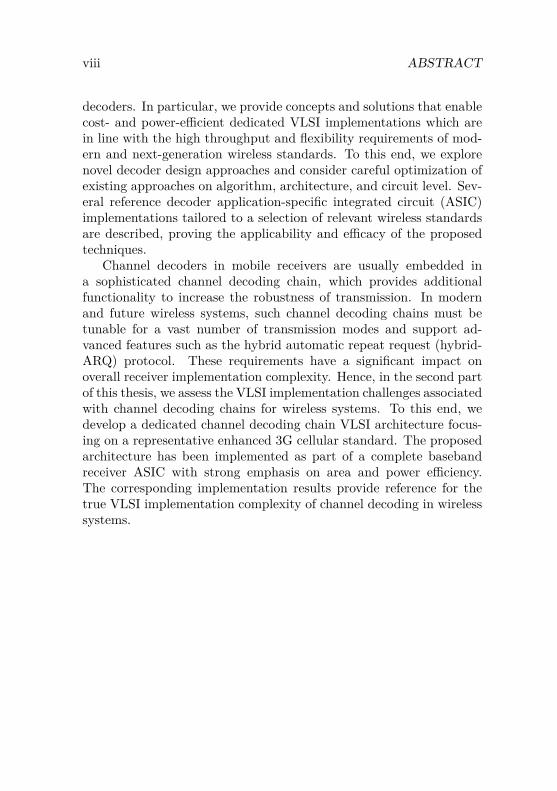
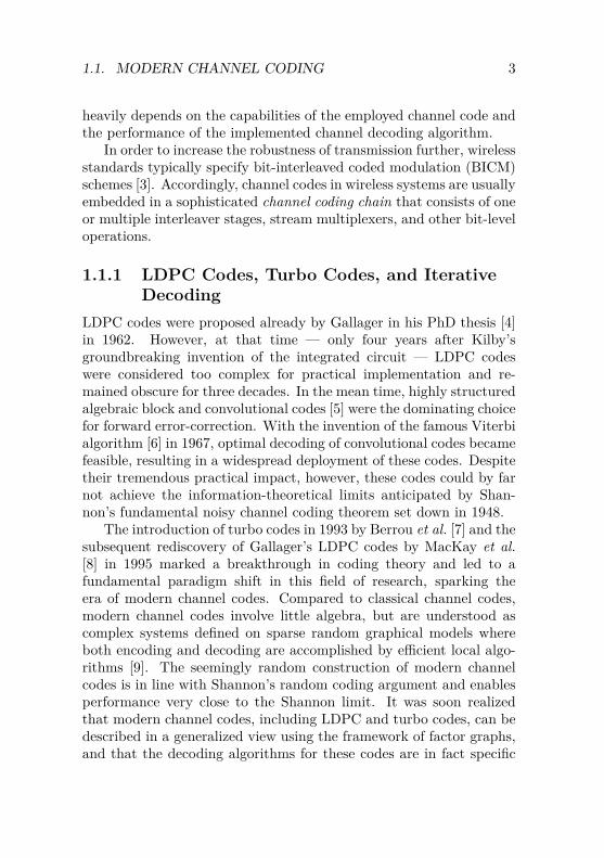
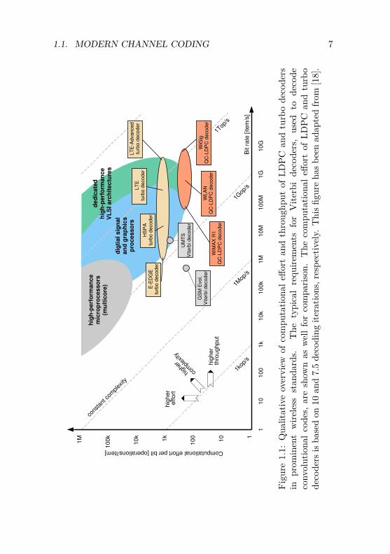
Computational Complexity Fig. 1.1 depicts the computationaleffort required for LDPC and turbo decoding in terms of operationsper bit against the throughput requirements of prominent wirelesssystems. The diagonal lines in the double-logarithmic scale are repre-sentative for the overall complexity (in terms of operations per second)that must be supported by corresponding hardware decoders. Itcan be generally observed that the complexity of LDPC and turbodecoders for present and emerging wireless systems is virtually ex-ploding. To meet these challenging complexity requirements, thesedecoders must be implemented as high-performance very-large-scaleintegration (VLSI) application-specific integrated circuit (ASIC) com-ponents in order to leverage the performance and power advantageof circuits realized in dedicated hardware [19, 20]. However, evenin ASIC designs implemented in deep-submicron CMOS technology,the large silicon area and power consumption of LDPC and turbodecoders pose a tremendous challenge to the wireless industry, whichnaturally targets battery-powered devices and which is firmly drivenby cost (i.e., silicon area) and time-to-market. It can also be concludedfrom Fig. 1.1 that the portfolio of LDPC and turbo decoders forwireless systems must span more than three orders of magnitudein terms of complexity as a consequence of the large range of datarate requirements found in the different standards deploying thesecodes (see Table 1.1). In order to cover this complexity range as effi-cient as possible with respect to silicon area and power consumption,one cannot simply rely on the advances in CMOS technology, buthas to devise new solutions and careful optimization on algorithm,architecture, and circuit level [19, 20].
Flexibility Requirements Link adaptation (LA) and hybrid au-tomatic repeat request (usually referred to as hybrid-ARQ or HARQ)
1.1. MODERN CHANNEL CODING 7
1Gop
/s
1Mop
/s
1kop
/s
cons
tant
com
plex
ity
1Top
/s
Computational effort per bit [operations/item]
WLAN
1k
10k
100k
1M 10
100 1
10
100
10k
1k
100k
10M
1M
100M
10G
1G
1
hig
her
thro
ughput
Bit r
ate
[item
/s]
hig
h-p
erf
orm
an
ce
mic
rop
rocesso
rs(m
ult
ico
re)
dig
tial sig
nal
an
d g
rap
hic
sp
rocesso
rs
ded
icate
dh
igh
-perf
orm
an
ce
VL
SI arc
hit
ectu
res
E-E
DG
Etu
rbo d
ecoder
HS
PA
turb
o d
ecoder
LT
Etu
rbo d
ecoder
LT
E-A
dvanced
turb
o d
ecoder
WLA
NQ
C-L
DP
C d
ecoder
WiM
AX
R1
QC
-LD
PC
decoder
WiG
igQ
C-L
DP
C d
ecoder
hig
her
effort
high
er
com
plex
ityG
SM
Evol.
Viterb
i decoder
UM
TS
Viterb
i decoder
Figu
re1.
1:Q
ualit
ativ
eov
ervi
ewof
com
puta
tiona
leffo
rtan
dth
roug
hput
ofLD
PCan
dtu
rbo
deco
ders
inpr
omin
ent
wire
less
stan
dard
s.T
hety
pica
lre
quire
men
tsfo
rV
iterb
ide
code
rs,
used
tode
code
conv
olut
iona
lcod
es,a
resh
own
aswe
llfo
rco
mpa
rison
.T
heco
mpu
tatio
nale
ffort
ofLD
PCan
dtu
rbo
deco
ders
isba
sed
on10
and
7.5
deco
ding
itera
tions
,res
pect
ivel
y.T
hisfi
gure
hasb
een
adap
ted
from
[18]
.
8 CHAPTER 1. INTRODUCTION
are key features in modern wireless standards. These technologiesenable high average throughput under the fast-varying transmissionenvironments encountered by mobile receiver terminals. In order to doso, the LA and HARQ operations schedule an efficient use of the radioresources relying on a tunable channel coding that can be adjustedin terms of block length (i.e., the length of the encoded messageblocks) and code rate (i.e., the amount of introduced redundancy)according to the present quality of the radio link and the decodingsuccess rate of received data packets. To this end, modern wirelessstandards typically foresee a wide range of operation modes, coveringblock lengths from several tens to several thousands of bits for alarge number of code rates, including very high3 code rates close to1. All these modes must be supported efficiently by a single highlyflexible decoder implementation. These stringent flexibility require-ments strongly exacerbate the challenge of channel decoder design forwireless systems.
1.2 Thesis ContributionsIn this thesis, we explore the VLSI implementation challenges of chan-nel decoding circuits for wireless systems. In particular, focusing onarchitectural transformations and careful optimization on algorithm,architecture, and circuit level, we provide concepts and solutions thatenable cost- and power-effective ASIC implementations that are in linewith the large range of throughput and flexibility requirements associ-ated with modern and next-generation wireless standards. While theinvestigations performed in this thesis are of general nature, we focusin our analysis on the binary QC-LDPC codes specified in the latestWLAN and WMAN standards and the binary parallel-concatenatedconvolutional turbo codes used in the 3GPP cellular standard suite.Reference decoder designs optimized for a selection of these practicallyrelevant standards have been implemented to prove the applicabilityand efficacy of the presented methods. Moreover, in addition tofocusing on stand-alone decoder implementations, we also explore
3A Code rate close to 1 means that almost no redundancy is included in thetransmitted bitstream. Especially in conjunction with HARQ, high code rateshave become an attractive operation mode in wireless systems.
1.2. THESIS CONTRIBUTIONS 9
the VLSI implementation challenges associated with the design ofcomplete channel decoding chains for wireless standards. To thebest of our knowledge, the VLSI circuits presented in this thesis arecurrently among the best-in-class found in the open literature.
In what follows, the key contributions of this thesis are describedin more detail.
VLSI Implementation of LDPC Decoding
LDPC codes turned out to be highly suitable for implementationin modern CMOS technology. The underlying decoding algorithmoffers large intrinsic parallelism, which has been exploited in manydecoder implementations to achieve very high throughput. However,the energy-efficient implementation of flexible high-throughput LDPCdecoders as required in recent and emerging wireless systems is still amajor challenge. A key concern in corresponding implementations isthe large amount of memory and the related highly parallel read/writememory access requirements. Due to these stringent memory accessrequirements, the memory components in flexible LDPC decoder im-plementations typically consume a dominant share of total power andthus represent a major power bottleneck.
Contributions We summarize and extend our contributions pub-lished in [21–24] on the energy-efficient VLSI implementation of flex-ible QC-LDPC decoders. A detailed study on the general architec-tural trade-offs in the design of LDPC decoders is provided, revealingthat the block-parallel architecture class is particularly suited for theimplementation of flexible QC-LDPC decoders [22]. Based on thisgeneric architecture class, we develop a highly scalable architecturethat can be configured at run-time to decode virtually any QC-LDPCcode. Moreover, different techniques for improving energy efficiencyof corresponding ASIC implementations are considered. In particular,an optimized low-power memory architecture based on standard-cellbased memory (SCM) blocks [23] is described as an approach totackle the large power consumption of the memory components. TwoQC-LDPC decoder ASIC prototypes in 90 nm CMOS based on thedescribed techniques and tailored to the specifics of the IEEE 802.11nWLAN standard are presented. Both ASICs clearly outperform prior
10 CHAPTER 1. INTRODUCTION
art in terms of energy efficiency and show outstanding throughputand silicon-efficiency metrics [21,24].
VLSI Implementation of Turbo Decoding
Turbo decoders have evolved from low-throughput serial implemen-tations to high-throughput subblock-parallel implementations. Whilestate-of-the-art turbo decoders are highly flexible with respect to theblock length they support, the impact of supporting the full rangeof code rates on the implementation complexity of practical turbodecoders has been addressed only marginally so far. In fact, tradi-tional turbo decoders found in the open literature were implementedwith focus on low code rate only and consequently achieve poor error-correction performance for high code rate. Furthermore, the area-efficient implementation of high-throughput subblock-parallel turbodecoders remains challenging, especially when high code rate hasto be supported. This is indicated by the fact that none of therecently reported decoder implementations reaches the 3 Gbps peakthroughput of LTE-A.
Contributions We summarize and extend our contributions pub-lished in [25–28]. In particular, we systematically explore existingand new architectural choices for flexible turbo decoders and evaluatethe associated VLSI implementation costs. The focus lies on sliding-window turbo decoders based on the BCJR algorithm and the soft-output Viterbi algorithm (SOVA), and we consider serial as well assubblock-parallel architectures.
For serial turbo decoders, we analyze the impact of supportinghigh code rate on silicon area and power consumption. We identifya specific architecture type that enables good error-correction perfor-mance for all code rates with comparably low memory requirements(and hence small area and power overhead) and prove its efficiencywith a detailed trade-off study [25]. Based on our findings, we describeflexible turbo decoder implementations optimized for the HSPA andthe E-EDGE standards in 180 nm CMOS [25,28]. The correspondingimplementation results demonstrate that our flexible designs are evenmore efficient in terms of silicon area and power consumption thanprior-art non-flexible decoders.
1.2. THESIS CONTRIBUTIONS 11
With respect to subblock-parallel turbo decoders, we focus ondecoder throughput and propose for the first time a systematic frame-work that enables a unified throughput evaluation of sliding-windowturbo decoder architectures, taking their individual trade-offs in termsof window length, error-rate performance and throughput into ac-count [27]. Based on this framework, existing architectures are com-pared, revealing that the support of high code rate has a strongimpact on the throughput of subblock-parallel turbo decoders, es-pecially for high degrees of subblock-parallelism. Moreover, we showthat the throughput of subblock-parallel decoders can be significantlyincreased by combining the strengths of existing architectures. Asa proof-of-concept, we provide a synthesis study in 65 nm CMOS ofthe discussed architectures optimized for LTE-A, which clearly showsthat our combined architecture also is the most efficient one in termsof area per throughput.
Design of a Complete Channel Decoding Chain for UMTS
In state-of-the-art digital baseband receiver implementations, the chan-nel decoder is typically realized as dedicated hardware accelerator,while the remaining functionality of the channel decoding chain isprovided by a software-programmable processor. The main advan-tages of this programmable architecture type are its large flexibilityand its short turn-around time. However, these advantages come ata significant cost overhead in terms of silicon area and power con-sumption compared to an optimized baseband receiver implementedin fully dedicated VLSI circuits.
Contributions We present a fully dedicated VLSI architecture ofa complete downlink channel decoding chain for TD-HSPA+ LCR,which is a typical representative of a 3G/3.75G cellular standard.The proposed architecture has been carefully optimized on top- andblock-level to support all possible operation modes with low siliconarea, low power consumption, and low latency. This includes thedesign and optimization of an efficient flexible Viterbi decoder thatforms together with the described turbo decoder a complete channeldecoder solution for all specified variants of the UMTS standard. Thedescribed channel decoding chain architecture has been integrated
12 CHAPTER 1. INTRODUCTION
in 130 nm CMOS technology as part of a digital downlink basebandreceiver ASIC for TD-HSPA+ LCR, designed and implemented incollaboration with other PhD students at the same research institute.Corresponding implementation results are provided.
1.3 Thesis OutlineThe remaining part of this thesis is organized as follows: Chapter 2reviews the essentials of LDPC codes and turbo codes in wirelessstandards, including the related techniques employed to tune blocklength and code rate. Furthermore, it discusses the underlying it-erative decoding algorithms with a strong focus on low-complexitysolutions that are most suitable for VLSI implementation.
Chapter 3 deals with the VLSI implementation of LDPC decoders.We initially focus on a high-level architecture exploration that leadsto the design of a highly flexible QC-LDPC decoder architecture.The second part of this chapter is then concerned with the energy-and area-efficient implementation of the presented architecture andprovides corresponding ASIC implementation results.
Chapter 4 addresses the VLSI design challenges of flexible turbodecoders. We first discuss best-practice and new implementationapproaches for serial and subblock-parallel turbo decoders and thenshow that the need for flexible code rate has a strong impact on theimplementation choices and costs of such decoders. In the second partof this chapter, we present our solutions — supported by ASIC imple-mentation results — to optimize the implementation costs of flexibleturbo decoder implementations with respect to their associated siliconarea, power consumption, and throughput.
In Chapter 5, we first provide an overview on the considered en-hanced 3G cellular communication standard and then describe theVLSI architecture and implementation of a complete channel decodingchain that supports all the operation modes provided by the standard.
Finally, the thesis is concluded in Chapter 6.
Chapter 2
Preliminaries
In this chapter, we review the basics of LDPC codes and turbo codesand describe best-practice with respect to related low-complexity it-erative decoding algorithms. To this end, we first introduce a genericsystem model and the terms that serve throughout this thesis as abasis for the evaluation of the decoding algorithms and related VLSIimplementations.
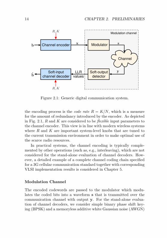
2.1 System ModelConsider the generic digital communication system shown in Fig. 2.1,which we divide into three main components: i) the channel encoder,ii) the modulation channel, and iii) the channel decoder. In whatfollows, these components are described in more detail.
Channel Encoder
In the transmitter, the channel encoder obtains K-dimensional blocksb = (b1, . . . , bK) of information bits bk ∈ {0, 1} and maps them intoN -dimensional binary-valued codewords x = (x1, . . . , xN ) using achannel-code specific bijective mapping function. We refer to K asblock length and N as codeword length, where N ≥ K. The encoderis called systematic if the information bits appear somewhere in thecodeword, usually in the first K positions. A fundamental metric in
13
14 CHAPTER 2. PRELIMINARIES
Channel encoder Modulator
Soft-outputdetector
Soft-inputchannel decoder
Channel
bx s
yb
R,K
R,K
Modulation channel
LLRvalues
Figure 2.1: Generic digital communication system.
the encoding process is the code rate R = K/N , which is a measurefor the amount of redundancy introduced by the encoder. As depictedin Fig. 2.1, R and K are considered to be flexible input parameters tothe channel encoder. This view is in line with modern wireless systemswhere R and K are important system-level knobs that are tuned tothe current transmission environment in order to make optimal use ofthe scarce radio resources.
In practical systems, the channel encoding is typically comple-mented by other operations (such as, e.g., interleaving), which are notconsidered for the stand-alone evaluation of channel decoders. How-ever, a detailed example of a complete channel coding chain specifiedfor a 3G cellular communication standard together with correspondingVLSI implementation results is considered in Chapter 5.
Modulation Channel
The encoded codewords are passed to the modulator which modu-lates the coded bits into a waveform s that is transmitted over thecommunication channel with output y. For the stand-alone evalua-tion of channel decoders, we consider simple binary phase shift key-ing (BPSK) and a memoryless additive white Gaussian noise (AWGN)
2.1. SYSTEM MODEL 15
channel model. Hence, each coded bit xn is mapped to a real-valuedsymbol sn ∈ {−
√Es,√Es}, where Es denotes the average symbol
energy, and the received N -dimensional signal vector consequentlybecomes y = s + w, with wn ∼ N (0, N0/2). The AWGN channel ischaracterized by its instantaneous signal-to-noise ratio (SNR), whichis defined in accordance with [5] as
SNR = EsRN0
= EbN0
, (2.1)
where Eb = Es/R denotes the average energy per transmitted infor-mation bit.
At the receiver, a soft-output detector computes reliability soft-information for each coded bit xn based on the observed channeloutputs y in the form of real-valued log-likelihood ratio (LLR) valuesaccording to
`n = log(
Pr[xn = 0|y]Pr[xn = 1|y]
). (2.2)
Intuitively, the sign of an LLR value `n indicates whether the corre-sponding coded bit xn is more likely a binary-0 or binary-1, whilethe magnitude represents the reliability of the estimate. For theconsidered setup described above, the computation of the LLR valuessimplifies to `n = 4yn/N0 [29].
Soft-Input Channel Decoder
The N channel LLR values ` = (`1, . . . , `N ) are fed to the soft-inputchannel decoder. The main task of the channel decoder is to processthe received LLR values and to generate an estimate x = (x1, . . . , xN )of the transmitted codeword by exploiting the redundancy introducedby the employed channel code under the knowledge of R and K.Based on the estimated codeword, an estimate b = (b1, . . . , bK) ofthe transmitted information bits is finally obtained.
With the communication channel being of statistical nature, thedecoding process is essentially a statistical detection problem. The
16 CHAPTER 2. PRELIMINARIES
ideal block maximum a-posteriori (MAP) decoder produces the mostlikely codeword given the channel LLRs, i.e.,
x = arg maxx′∈C
Pr[x′|`], (2.3)
where C denotes the set of all valid codewords defined by the employedchannel code. The symbol MAP decoder produces an estimate of eachcoded bit according to
xn = arg maxx′∈{0,1}
Pr[x′|`]. (2.4)
The maximum-likelihood (ML) decoder delivers the codeword thatmaximizes the probability of the received LLR values, i.e.,
x = arg maxx′∈C
Pr[`|x′]. (2.5)
The ML decoder coincides with the block MAP decoder if the code-words are uniformly distributed over C. All these ideal decoders canbe practically implemented only for small or highly structured codes.For convolutional codes, for instance, the famous Viterbi algorithm [6]enables ML decoding, while the forward/backward algorithm by Bahl,Cocke, Jelinek, and Raviv [30], also referred to as the BCJR or MAPalgorithm, allows for efficient symbol MAP decoding. For more power-ful codes, however, practical decoders are only approximations of theseideal decoders. We will see that the standard sub-optimal decodingalgorithms for LDPC codes and turbo codes are iterative algorithmsthat are run for a predefined number of I iterations. In general, thesealgorithms improve the estimate of the codeword with every iterationbefore the improvements diminish and eventually saturate after acode specific amount of performed iterations. In order to quantifythe reliability of the estimates provided by the decoders for a specificSNR and I, we will consider the bit error-rate (BER) Pr[bk 6= bk] orsometimes also the block error-rate (BLER) Pr[b 6= b].
With respect to practical decoder implementations, I is a crucialparameter as it impacts proportionally on the computational com-plexity of the decoding algorithm and the energy dissipation. Hence,I must be carefully evaluated in practical systems to ensure a goodtrade-off between computational complexity, energy efficiency, and
2.2. LOW-DENSITY PARITY-CHECK CODES 17
error-rate performance. As measure for energy efficiency we willconsider throughout this thesis the energy per bit of the decoder or theenergy per bit per iteration, and it will become clear from the specificcontext whether the measure refers to the information bits at the out-put of the decoder or the codeword bits at the input. In order to avoidredundant iterations early termination can be performed by the de-coder. Early termination stops decoding when further iterations seemunlikely to alter the result based on an online stopping criterion thattracks the convergence of the iterative decoding process. Obviously,early termination is desirable in practical decoder implementations toreduce the average energy dissipation of the decoder.
In the following two sections, we will describe the most prominentpractical decoding algorithms for LDPC and turbo codes in moredetail and evaluate the related error-rate performance.
2.2 Low-Density Parity-Check Codes
A binary LDPC code is a linear block code and can therefore bedescribed by a binary-valued M×N parity-check matrix H accordingto
Hx> = 0M×1 (2.6)
in GF(2), where 0M×1 denotes the M -dimensional all-zero vector andM = N−K. Each row in H describes a parity-check equation and thecolumns define how the N coded bits participate in these parity-checkequations. As the name suggests, an LDPC code has the additionalfundamental property that the parity-check matrix is sparse, i.e.,contains only a small number of non-zero entries. A distinction ismade between regular LDPC codes and irregular LDPC codes. Theparity-check matrix of a regular LDPC code exhibits a fixed small rowdegree (i.e., Hamming weight) and a (different) fixed small columndegree. For irregular LDPC codes, the row and column degrees aredescribed statistically by degree distributions.
18 CHAPTER 2. PRELIMINARIES
VN 2
CN M
VN NVN 1
CN 1
x1 x2 xN
sparse pseudo-random connection network
Figure 2.2: Generic factor graph of an LDPC code.
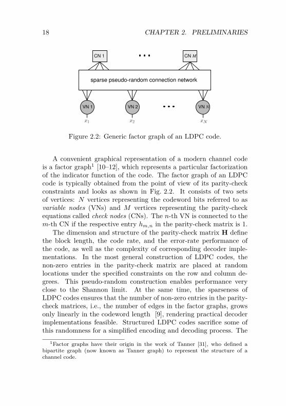
A convenient graphical representation of a modern channel codeis a factor graph1 [10–12], which represents a particular factorizationof the indicator function of the code. The factor graph of an LDPCcode is typically obtained from the point of view of its parity-checkconstraints and looks as shown in Fig. 2.2. It consists of two setsof vertices: N vertices representing the codeword bits referred to asvariable nodes (VNs) and M vertices representing the parity-checkequations called check nodes (CNs). The n-th VN is connected to them-th CN if the respective entry hm,n in the parity-check matrix is 1.
The dimension and structure of the parity-check matrix H definethe block length, the code rate, and the error-rate performance ofthe code, as well as the complexity of corresponding decoder imple-mentations. In the most general construction of LDPC codes, thenon-zero entries in the parity-check matrix are placed at randomlocations under the specified constraints on the row and column de-grees. This pseudo-random construction enables performance veryclose to the Shannon limit. At the same time, the sparseness ofLDPC codes ensures that the number of non-zero entries in the parity-check matrices, i.e., the number of edges in the factor graphs, growsonly linearly in the codeword length [9], rendering practical decoderimplementations feasible. Structured LDPC codes sacrifice some ofthis randomness for a simplified encoding and decoding process. The
1Factor graphs have their origin in the work of Tanner [31], who defined abipartite graph (now known as Tanner graph) to represent the structure of achannel code.
2.2. LOW-DENSITY PARITY-CHECK CODES 19
class of QC-LDPC codes [16, 17] provides a particularly favorabletrade-off between error-correction performance (especially for shortblock lengths) and implementation complexity [32]. For this reason,many of the LDPC codes employed in recent and emerging wirelesscommunication standards belong to this class.
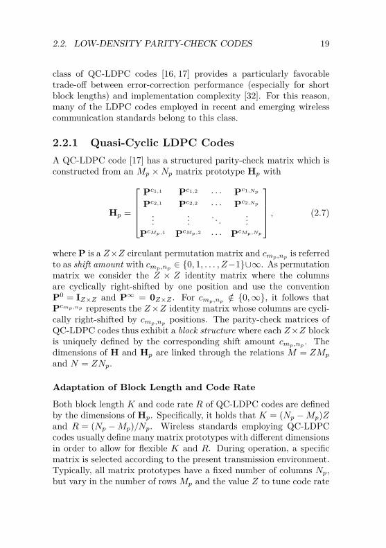
2.2.1 Quasi-Cyclic LDPC CodesA QC-LDPC code [17] has a structured parity-check matrix which isconstructed from an Mp ×Np matrix prototype Hp with
Hp =
Pc1,1 Pc1,2 · · · Pc1,Np
Pc2,1 Pc2,2 · · · Pc2,Np
...... . . . ...
PcMp,1 PcMp,2 · · · PcMp,Np
, (2.7)
where P is a Z×Z circulant permutation matrix and cmp,np is referredto as shift amount with cmp,np ∈ {0, 1, . . . , Z−1}∪∞. As permutationmatrix we consider the Z × Z identity matrix where the columnsare cyclically right-shifted by one position and use the conventionP0 = IZ×Z and P∞ = 0Z×Z . For cmp,np
/∈ {0,∞}, it follows thatPcmp,np represents the Z×Z identity matrix whose columns are cycli-cally right-shifted by cmp,np positions. The parity-check matrices ofQC-LDPC codes thus exhibit a block structure where each Z×Z blockis uniquely defined by the corresponding shift amount cmp,np
. Thedimensions of H and Hp are linked through the relations M = ZMp
and N = ZNp.
Adaptation of Block Length and Code Rate
Both block length K and code rate R of QC-LDPC codes are definedby the dimensions of Hp. Specifically, it holds that K = (Np −Mp)Zand R = (Np −Mp)/Np. Wireless standards employing QC-LDPCcodes usually define many matrix prototypes with different dimensionsin order to allow for flexible K and R. During operation, a specificmatrix is selected according to the present transmission environment.Typically, all matrix prototypes have a fixed number of columns Np,but vary in the number of rows Mp and the value Z to tune code rate
20 CHAPTER 2. PRELIMINARIES
and block length, respectively. For instance, the IEEE 802.11n WLANstandard [33] specifies 12 different matrix prototypes with Np = 24,Z ∈ {27, 54, 81}, and Mp ∈ {4, 6, 8, 12}, i.e., R ∈ {5/6, 3/4, 2/3, 1/2}.The IEEE 802.16 WiMAX standard [34] specifies even 114 differentmodes with parameters that are similar to the ones found in WLAN.
2.2.2 Decoding of LDPC CodesAn LDPC code is usually decoded by performing message-passing(also known as belief propagation) along the edges of the associatedfactor graph relying on the sum-product algorithm [11,12], which hasbecome the standard decoding algorithm for modern channel codes.The message outgoing from a specific node in the graph representsthe marginal probability of the variable associated with the respectiveedge, summarizing all variables in the subsystem behind the consid-ered node. For cycle-free graphs, the message-passing terminates andthe computed marginals are exact. In this case, the sum-product algo-rithm is an optimal non-iterative symbol MAP decoder in accordancewith the definition in (2.4). If the graph has cycles — as it is thecase for LDPC codes — message-passing has no termination and thesum-product algorithm becomes an iterative approximate algorithm.Although iterative message-passing is in general not guaranteed toconverge, it has been empirically proven to be highly successful forboth LDPC codes and turbo codes.
We denote the message passing from the n-th VN to the m-thCN as Q-message Qn,m and the message passing from the m-th CNto the n-th VN as R-message Rm,n. The sum-product algorithm istypically formulated in the LLR domain. In this case, all messagesare LLR values, and the result of the decoder for each codeword bitxn is an iteratively improving estimate of the respective a-posterioriLLR value. We refer to these estimates as L-values Ln, i.e.,
Ln ≈ log(
Pr[xn = 0|`]Pr[xn = 1|`]
). (2.8)
Fig. 2.3 shows the factor graph of an example QC-LDPC code with anillustration of the introduced messages and values. The order of up-dating the messages and values in each iteration is called the message-passing schedule. With the conventional flooding schedule [11] each
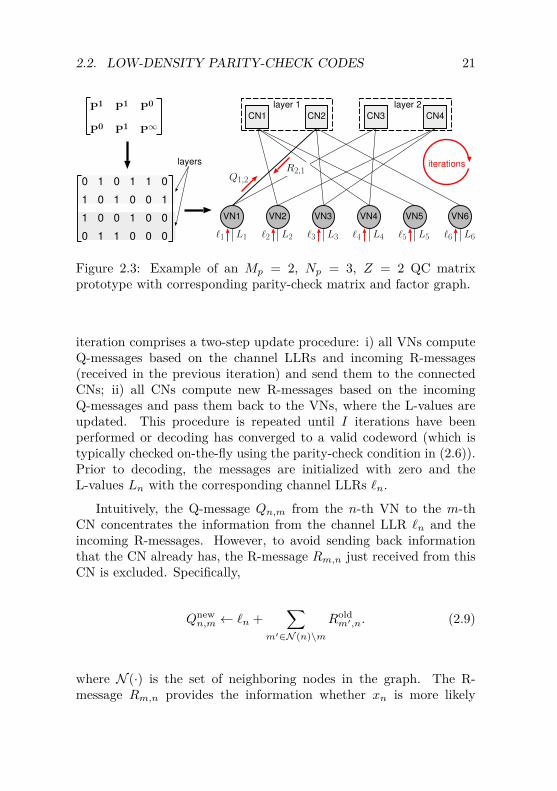
2.2. LOW-DENSITY PARITY-CHECK CODES 21
VN1 VN2 VN3 VN4
CN2 CN3
VN5 VN6
CN1 CN4
0 1 0 1 1 0
1 0 1 0 0 1
1 0 0 1 0 0
0 1 1 0 0 0
Q1,2
R2,1iterations
L1 L2 L3 L4 L5 L6
P1 P0
P∞
P1
P1P0
layers
ℓ1 ℓ2 ℓ3 ℓ4 ℓ5 ℓ6
layer 1 layer 2
Figure 2.3: Example of an Mp = 2, Np = 3, Z = 2 QC matrixprototype with corresponding parity-check matrix and factor graph.
iteration comprises a two-step update procedure: i) all VNs computeQ-messages based on the channel LLRs and incoming R-messages(received in the previous iteration) and send them to the connectedCNs; ii) all CNs compute new R-messages based on the incomingQ-messages and pass them back to the VNs, where the L-values areupdated. This procedure is repeated until I iterations have beenperformed or decoding has converged to a valid codeword (which istypically checked on-the-fly using the parity-check condition in (2.6)).Prior to decoding, the messages are initialized with zero and theL-values Ln with the corresponding channel LLRs `n.
Intuitively, the Q-message Qn,m from the n-th VN to the m-thCN concentrates the information from the channel LLR `n and theincoming R-messages. However, to avoid sending back informationthat the CN already has, the R-message Rm,n just received from thisCN is excluded. Specifically,
Qnewn,m ← `n +
∑m′∈N (n)\m
Roldm′,n. (2.9)
where N (·) is the set of neighboring nodes in the graph. The R-message Rm,n provides the information whether xn is more likely
22 CHAPTER 2. PRELIMINARIES
binary-0 or binary-1 based on the m-th parity-check and the infor-mation received from all other VNs participating in this check, whichcan be described as [11]
Rnewm,n ← 2 tanh−1
∏n′∈N (m)\n
tanh(Qnewn′,m
2
) . (2.10)
The L-value Ln at the n-th VN is composed of the input channel LLR`n and all incoming R-messages, i.e., the information extracted fromthe parity-check constraints, according to
Lnewn ← `n +
∑m′∈N (n)
Rnewm′,n. (2.11)
The final estimate xn is obtained from the sign of the correspondingL-value. In this thesis only systematic LDPC codes are considered.Hence, the first K xn correspond to the estimated information bitsbk. Note that for the first few iterations (before any cycle in the graphcloses), the R-messages at the n-th VN are independent of the inputchannel LLR `n. In subsequent iterations, these parameters becomecorrelated as soon as the input LLR returns back to the VN throughcycles in the graph. It is this cycle-induced correlation that renders thealgorithm approximate. The characteristics of the cycles in the graphstrongly influence the convergence of iterative message-passing [8,11].Short cycles, especially length-4 cycles, have a detrimental impact andare thus avoided in the construction of practical LDPC codes.
Layered Message-Passing Schedule
A superior approach to the flooding schedule is the layered sched-ule [35], which partitions the computation in each iteration into severallayers that correspond to distinct subsets of rows of H. For each layer,only the CNs related to the current layer receive Q-messages and passtheir R-messages back to the connected VNs, which in turn updateboth L-values and Q-messages. Then, the next layer is processedsimilarly. As with the flooding schedule, all messages are initializedwith zero and the L-values with the channel LLRs prior to decoding.
2.2. LOW-DENSITY PARITY-CHECK CODES 23
The advantage of this schedule is that the information gained forLn in each layer is considered already in the processing of the sub-sequent layer during the same iteration. With proper layer selection,this schedule generally leads to faster convergence, eventually reducingthe number of iterations required to achieve a target BER roughly bya factor of two [35]. Due to the faster convergence speed, layereddecoder implementations generally exhibit lower silicon complexityfor a given throughput constraint and better energy efficiency thantheir flooding based counterparts [22]. As shown in [35], a particularfavorable layer selection in terms of convergence speed and implemen-tation complexity is achieved if the CNs are partitioned into O layersL1, . . . ,LO such that no two CNs in a layer are connected to the sameVN or, equivalently, such that each VN in a layer has degree 1, i.e., isconnected to only one CN. Formally, this condition is expressed as
N (m) ∩N (m′) = ∅ ∀i ∈ {1, . . . , O}, ∀m,m′ ∈ Li. (2.12)
Note that (2.12) is trivially satisfied if the layers coincide with therows of H. For QC-LDPC codes as in (2.7), such a layer selectionis also achieved if the layers coincide with the O = Mp rows of thematrix prototype Hp (see example in Fig. 2.3). It is important tonote that the per-layer updates of L-values and Q-messages can besubstantially simplified if the layers are selected as in (2.12) becauseeach VN in any layer only receives one new R-message in this case.In particular, from (2.9) and (2.11) with the relaxed constraint thatonly one R-message arrives at the VN in any layer it follows that thenew Q-message Qn,m can be computed from the current L-value Lnand the arriving R-message according to [35]
Qnewn,m ← Lold
n −Roldm,n. (2.13)
The L-value update simplifies accordingly to
Lnewn ← Qnew
n,m +Rnewm,n. (2.14)
Note that, in contrast to the flooding schedule, no separate memoriesfor L-values and channel LLRs are required with this scheme.
24 CHAPTER 2. PRELIMINARIES
Low-Complexity Message Update Rules
The original CN update rule in (2.10) involves the use of transcen-dental functions, which are ill-suited for VLSI implementation. Astraightforward approximation is known as the min-sum algorithm [36].Here, the odd symmetry and monotonicity of the tanh function areexploited to use an approximation based on simple min-operations.The resulting complexity reduction, however, comes at the expenseof a significant loss in terms of error-rate performance. This losscan be mitigated to a great extent by either adding a normalizationfactor to the min-sum algorithm or by conditioning the messagesprovided by the min-sum algorithm with a simple offset [37]. In theremainder of this thesis, we consider the latter approach known as theoffset-min-sum (OMS) algorithm which simplifies (2.10) to
Rnewm,n ← max
(min
n′∈N (m)\n|Qnew
n′,m| − β, 0) ∏n′∈N (m)\n
sign(Qnewn′,m).
(2.15)
where the offset β serves as an empirical correction factor. Withrespect to practical decoder implementations, we will see in Chapter 3that it is useful to break the computation in (2.15) into two steps [32],which we refer to as MIN step and SEL step, respectively. Duringthe MIN step, the first and second minima min1 and min2 of allincoming Q-message magnitudes and the index minIdx of the firstminimum along with the sign of all Q-messages are obtained as
min1 = minn′∈N (m)
|Qnewn′,m| (2.16)
minIdx = arg minn′∈N (m)
|Qnewn′,m| (2.17)
min2 = minn′∈N (m)\minIdx
|Qnewn′,m| (2.18)
sign =∏
n′∈N (m)
sign(Qnewn′,m). (2.19)
2.2. LOW-DENSITY PARITY-CHECK CODES 25
During the SEL step, the proper minimum value is selected and theR-message updated according to
min ={
min2 when n = minIdxmin1 otherwise
(2.20)
Rnewm,n ← sign · sign(Qnew
n,m) ·max (min − β, 0) . (2.21)
Error-Rate Performance Comparison
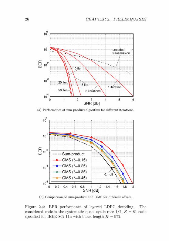
In Fig. 2.4, the simulated BER performance of a layered QC-LDPCdecoder for the systematic rate-1/2, Z = 81 code of IEEE 802.11n [33]is analyzed. The considered code has a block length K = 972 and thusa codeword length N = 1944. The simulation has been performed overan AWGN channel with BPSK modulation as described in Sec. 2.1.
In Fig. 2.4(a) we first compare the BER performance of the originalsum-product algorithm for different number of iterations I. It can beobserved that the BER performance improves considerably for smallI and saturates roughly after 25 to 30 iterations. Practical decoderimplementations found in the open literature typically perform 5 to10 iterations.
Fig. 2.4(b) compares the BER performance of the sum-productand OMS algorithms at I = 10 iterations for different offsets β.Surprisingly, for the best evaluated offset β = 0.45, the low-complexityOMS algorithm shows a very small SNR loss of less than 0.1 dB com-pared to the original sum-product algorithm. This loss is negligiblein typical applications for wireless systems.
26 CHAPTER 2. PRELIMINARIES
0 1 2 3 4 5 610
-4
10-3
10-2
10-1
100
BE
R
SNR [dB]
uncodedtransmission
1 iteration
2 iterations
5 iter.
10 iter.
20 iter.
50 iter.
(a) Performance of sum-product algorithm for different iterations.
0 0.2 0.4 0.6 0.8 1 1.2 1.4 1.6 1.8 210
-4
10-3
10-2
10-1
100
BE
R
Sum-product
OMS (β=0.15)
OMS (β=0.25)
OMS (β=0.35)
OMS (β=0.45)
SNR [dB]
0.1 dB
(b) Comparison of sum-product and OMS for different offsets.
Figure 2.4: BER performance of layered LDPC decoding. Theconsidered code is the systematic quasi-cyclic rate-1/2, Z = 81 codespecified for IEEE 802.11n with block length K = 972.
2.3. TURBO CODES 27
bk
Inter-
leaver
1st component encoder
2nd component encoder
Pu
nctu
rer
xp2k
xp1k
xsk
K
R
bπ(k)
P/S
me
rge
r
xn
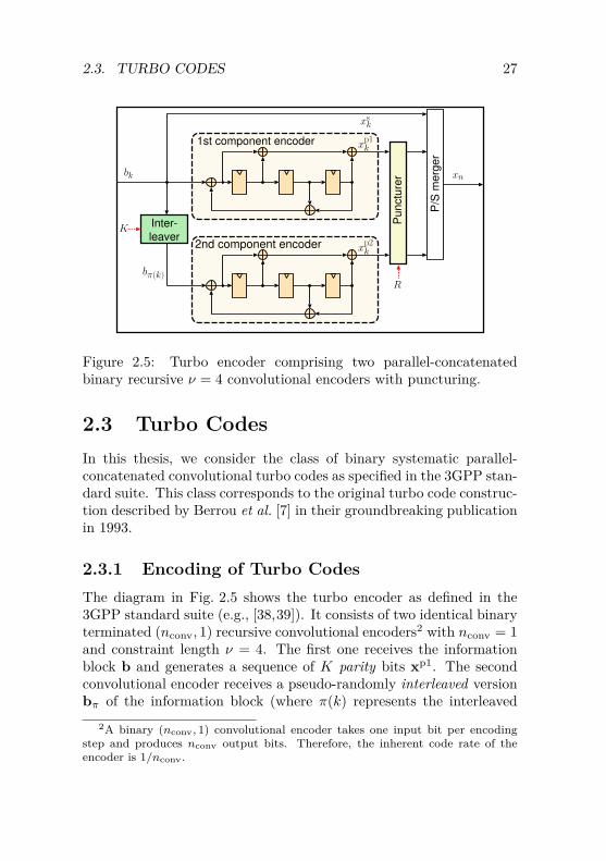
Figure 2.5: Turbo encoder comprising two parallel-concatenatedbinary recursive ν = 4 convolutional encoders with puncturing.
2.3 Turbo CodesIn this thesis, we consider the class of binary systematic parallel-concatenated convolutional turbo codes as specified in the 3GPP stan-dard suite. This class corresponds to the original turbo code construc-tion described by Berrou et al. [7] in their groundbreaking publicationin 1993.
2.3.1 Encoding of Turbo CodesThe diagram in Fig. 2.5 shows the turbo encoder as defined in the3GPP standard suite (e.g., [38,39]). It consists of two identical binaryterminated (nconv, 1) recursive convolutional encoders2 with nconv = 1and constraint length ν = 4. The first one receives the informationblock b and generates a sequence of K parity bits xp1. The secondconvolutional encoder receives a pseudo-randomly interleaved versionbπ of the information block (where π(k) represents the interleaved
2A binary (nconv, 1) convolutional encoder takes one input bit per encodingstep and produces nconv output bits. Therefore, the inherent code rate of theencoder is 1/nconv.
28 CHAPTER 2. PRELIMINARIES
index of k) and generates a second block of K parity bits xp2. Theinformation bits are forwarded to the output of the encoder as sys-tematic bitstream xs = b.
Adaptation of Block Length and Code Rate
The core of the encoder shown in Fig. 2.5 produces three bits perinput bit. Therefore, the inherent code rate of the turbo code isRTC = 1/3.3 As illustrated in Fig. 2.5, higher code rates are obtainedby puncturing, i.e., removing some of the parity bits at the outputof the encoder before the two parity bitstreams are merged togetherwith the systematic bitstream into the final codeword x. Observethat puncturing enables a very fine-grained tuning of the code rate.Interestingly, with the specification of the hybrid-ARQ feature in theHSDPA enhancement of UMTS, very high code rates close to 1 havebecome an attractive operation mode in wireless systems. Hence,corresponding turbo decoder implementations must support the fullrange of code rates from RTC up to R close to 1.
The valid block lengths K of the turbo code are defined by thespecified interleaver. Practical interleavers typically support a widerange of block lengths. For instance, the UMTS standard and itsenhancements HSPA, HSPA+ as well as the E-EDGE standard allspecify the same block interleaver [38] that supports all block lengthsfrom 40 to 5114. The LTE and LTE-A standards both specify aquadratic permutation-polynomial (QPP) interleaver [39,40] that sup-ports 188 block lengths between 40 and 6144.
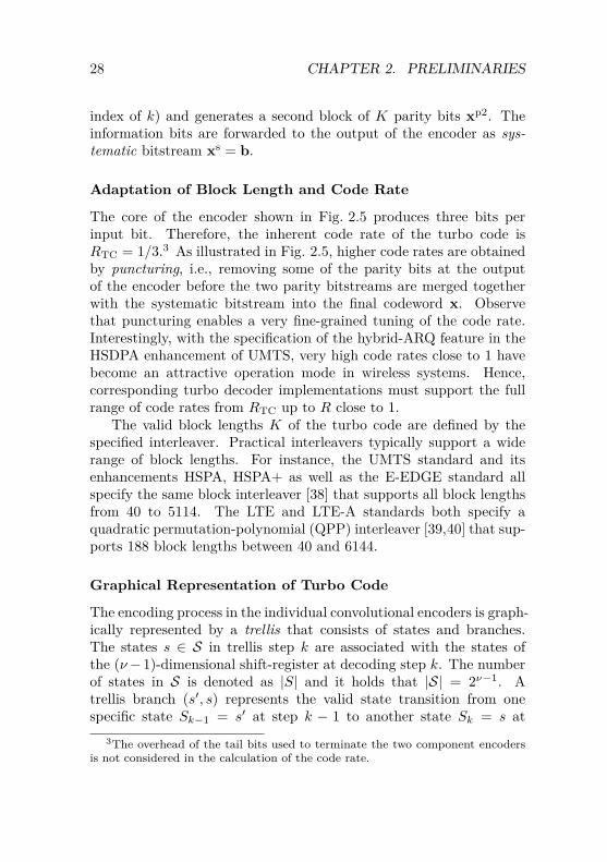
Graphical Representation of Turbo Code
The encoding process in the individual convolutional encoders is graph-ically represented by a trellis that consists of states and branches.The states s ∈ S in trellis step k are associated with the states ofthe (ν−1)-dimensional shift-register at decoding step k. The numberof states in S is denoted as |S| and it holds that |S| = 2ν−1. Atrellis branch (s′, s) represents the valid state transition from onespecific state Sk−1 = s′ at step k − 1 to another state Sk = s at
3The overhead of the tail bits used to terminate the two component encodersis not considered in the calculation of the code rate.
2.3. TURBO CODES 29
VN 1 VN KVN 2
xs1 xs2 xsK
xp11 x
p12 x
p1K
xp21 x
p22 x
p2K
pseudo-random connection network
xsπ(1) xsπ(2) xsπ(K)
s0
s1
s2
s3
s4
s5
s6
s7
(s0, s0)
(s1, s0)
kk-1
bk = 0
bk = 1
Figure 2.6: Graphical representation of turbo codes. Left: trellis ofconvolutional encoder. Right: trellis constrained factor graph of turbocode.
step k, induced by the structure of the convolutional encoder and theincoming information bit. The left-hand part of Fig. 2.6 shows the|S| = 8 state trellis of the considered binary convolutional encoders.
The graphical representation, i.e., factor graph, of the overall turbocode is typically obtained from the viewpoint of its trellis constraints(rather than parity-check constraints as for LDPC codes) and looksas shown in right-hand part of Fig. 2.6. Observe that this graph iscomposed of the two component trellises that are connected througha pseudo-random connection network defined by the properties of theinterleaver. The VN vertices are identical to the ones introducedfor the LDPC codes. The nodes in the trellis segments representthe different trellis steps and indicate for each trellis step the validcombination of left states s′, coded bits, and right states s [11, 12].
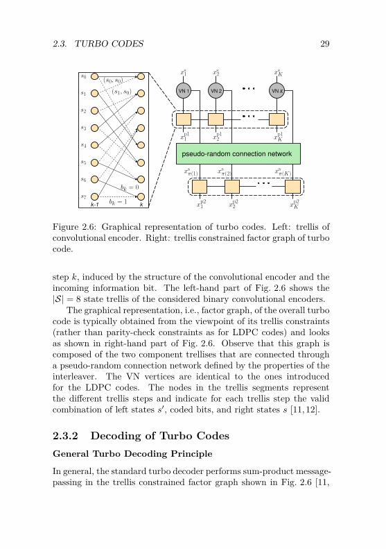
2.3.2 Decoding of Turbo CodesGeneral Turbo Decoding Principle
In general, the standard turbo decoder performs sum-product message-passing in the trellis constrained factor graph shown in Fig. 2.6 [11,
30 CHAPTER 2. PRELIMINARIES
1st SISO component
decoder
2nd SISOcomponent
decoder
LE2k
LA1k
LE1k
LA2k
Lsk
Lp1k
Lp2k
LD1k , bk
turbo
iterations
De
pu
nctu
rer
LD2k , bk
Inter-leaver
Inter-leaver
Deinter-leaver
Figure 2.7: Turbo decoder based on SISO component decoders asoriginally proposed by Berrou et al. [7].
12]. Since the graph has cycles, the sum-product algorithm becomesan approximate iterative algorithm. The standard message-passingschedule used in turbo decoders is known as the turbo schedule. Withthis schedule, an iteration is split into two half-iterations, and ineach half-iteration the messages in one of the two component trellisesare updated, while the messages in the second component trellis arefrozen.
The message-passing inside the component trellises is a generaliza-tion of soft-input soft-output (SISO) trellis decoding. For this reason,an equivalent yet more popular and insightful interpretation of thedecoding process is the one depicted in Fig. 2.7. Note that this in-terpretation coincides with the original formulation of turbo decodingby Berrou et al. [7]. The corresponding turbo decoder comprises twoSISO decoders. During the odd half-iterations, the first SISO decoderdecodes the first component convolutional code, while the second SISOdecoder is idle. During the even half-iterations, the first SISO decoderis idle and the second one decodes the second convolutional code. Af-ter odd half-iterations, the first SISO decoder passes soft-informationextracted from the convolutional code through the interleaver to theother SISO decoder. The exchanged soft-information is referred to asextrinsic information and summarizes the information gathered forthe systematic codeword bits via the constraints of the convolutionalcode. For the second SISO decoder, this information acts as a-priori
2.3. TURBO CODES 31
information which, due to the randomness of the interleaver, appearsto come from an independent source. It allows the second SISOdecoder to obtain a more accurate set of extrinsic information, whichis then passed back to the first SISO decoder as a-priori information.It is this iterative exchange of extrinsic soft-information together withthe randomization induced by the interleaver that makes turbo codesso powerful.
Specific Description
Prior to decoding, the received channel LLR values `n are depunc-tured (i.e., all-zero neutral LLR values are inserted at the locationsof punctured parity bits) and split into the three streams Ls
k, Lp1k ,
Lp2k that are associated with the encoded systematic bits and the two
parity bitstreams, respectively. In addition, a-priori LLRs LA1k , LA2
k
associated with each systematic bit are initialized with zero for bothcomponent decoders. Each iteration comprises a pass of the firstSISO decoder followed by a pass of the second one. The i-th SISOdecoder (i = 1, 2) first computes intrinsic a-posteriori LLRs LDi
k foreach systematic bit via the constraints of the convolutional code as
LDik = log
(Pr[xs
k = 0|Li]Pr[xs
k = 1|Li]
), (2.22)
where Li contains all Lsk, Lpi
k , and LAik . During odd half-iterations,
the first SISO decoder decodes the first component code and generatesLD1k relying on Ls
k, Lp1k , and LA1
k . The extrinsic LLRs LE1k reflect the
new information gathered by the SISO decoder, excluding the oldinformation already known by the other SISO decoder, i.e.,
LE1k = LD1
k − (Lsk + LA1
k ). (2.23)
These extrinsic LLR values serve as a-priori LLRs LA2k for the second
component decoder after being interleaved, i.e., LA2k = LE1
π(k). Duringeven half-iterations, the second SISO decoder in turn decodes thesecond code and generates LD2
k and the extrinsic LLR values
LE2k = LD2
k − (Lsπ(k) + LA2
k ), (2.24)
32 CHAPTER 2. PRELIMINARIES
which become the new a-priori LLRs LA1k = LE2
π−1(k) for the first SISOdecoder. This process is repeated until a predefined number of Ih = 2Ihalf-iterations is reached or early termination is triggered. At the endof decoding, hard-estimates bk of the information bits are obtainedbased on the sign of the corresponding intrinsic a-posteriori LLRs.The convergence behavior of the turbo code strongly depends on thestructure of the interleaver. In the practical construction of inter-leavers, a trade-off is thus typically sought for between performanceand suitability for implementation.
The algorithm performed in the SISO decoders strongly affectsthe error-rate performance and VLSI implementation complexity ofthe turbo decoder. The forward/backward or BCJR algorithm [30] isan optimal symbol MAP decoder for convolutional codes and yieldsthe exact a-posteriori LLR values in (2.22). Interestingly, it canbe shown that it coincides with sum-product message-passing per-formed in the trellis of convolutional codes [11]. In addition to itsoptimal performance, the BCJR algorithm is in general well-suitedfor implementation. For these reasons, it has become the de-factostandard choice for SISO decoding. An alternative to the BCJRalgorithm is the soft-output Viterbi algorithm (SOVA) [41], which,however, provides only an estimate of (2.22) but comes with reducedcomplexity [42]. Due to its sub-optimal performance, the SOVA hasonly been marginally considered in practical implementations. How-ever, several improvements to the original SOVA have been proposedrecently (e.g., [43, 44]), rendering the application of this algorithmin practical designs promising. In what follows, both algorithms arebriefly described. To simplify the ensuing exposition, we consider thefirst SISO decoder and drop the index i for the remainder of thissection.
2.3.3 The BCJR Algorithm
The BCJR algorithm [30] is able to compute the intrinsic a-posterioriLLRs in (2.22) exactly. To this end, it builds on the fact that a statetransition in the trellis at step k uniquely defines the systematic bitxsk. From this observation it follows that the probability of xs
k = b
2.3. TURBO CODES 33
corresponds to the sum of probabilities of state transitions associatedwith xs
k = b. Hence, (2.22) can be expressed as
LDk = log
∑
(s′,s):xsk=0
Pr[Sk−1 = s′, Sk = s,L]∑(s′,s):xs
k=1
Pr[Sk−1 = s′, Sk = s,L]
. (2.25)
The starting point of the BCJR algorithm is the observation that theprobabilities in (2.25) can be structured as [30,45]
Pr[Sk−1 = s′, Sk = s,L] = αk−1(s′) · γk(s′, s) · βk(s), (2.26)
where
αk−1(s′) = Pr[Sk−1 = s′,L1,k−1], (2.27)γk(s′, s) = Pr[Sk = s,Lk,k|Sk−1 = s′], (2.28)βk(s) = Pr[Lk+1,K |Sk = s], (2.29)
and Lk,k′ contains all Ls, Lp, and LA from trellis step k to k′. Thevalue αk−1(s′) is the probability that the trellis at step k−1 is in states′ under the LLRs observed up to this point. βk(s) is the probabilityat step k that the future LLRs will be Lk+1,K given that the trellis isin state s. Finally, γk(s′, s) is the probability that given the trellis is instate s′ at step k−1 it moves to state s and the observed LLRs at thisstep are Lk,k. The beauty of the BCJR algorithm is that the abovevalues αk−1(s′) and βk(s) can be calculated recursively as [30,45]
αk(s) =∑s′∈S
αk−1(s′)γk(s′, s), (2.30)
βk−1(s′) =∑s∈S
βk(s)γk(s′, s). (2.31)
Hence, the BCJR algorithm amounts to a forward recursion (2.30)from the beginning of the trellis to its end and a backward recursion(2.31) in opposite direction. The values αk(s) are referred to asforward state metrics and the βk(s) as backward state metrics. Thevalues γk(s′, s) are called branch metrics. Typically, the forwardrecursion is performed first, followed by the backward recursion and
34 CHAPTER 2. PRELIMINARIES
the concurrent computation of the a-posteriori LLRs according to(2.25) and (2.26). Note that only the valid state transitions de-fined by the trellis structure need to be considered in (2.30) and(2.31). For all other transitions, it holds that γk = 0. For terminatedtrellises that evolve from the all-zero state and end in the all-zerostate, the recursions are initialized with α0(s0) = βK(s0) = 1 andwith α0(s) = βK(s) = 0∀s 6= s0. The branch metrics in (2.28) can becalculated using the input LLR values according to
γk(s′, s) ∝exp( 1
2 (1 + µs(s′, s))(Lsk + LA
k ))1 + exp(Ls
k + LAk )
exp( 12 (1 + µp(s′, s))Lp
k)1 + exp(Lp
k) ,
(2.32)
where µs(s′, s) ∈ {−1, 1} and µp(s′, s) ∈ {−1, 1} correspond to thesystematic and parity bit, respectively, at the output of the encoderwhen the state transition (s′, s) occurs, with the convention thatbinary-0 is converted to µ = 1 and binary-1 to µ = −1.
A common approach to circumvent the costly multiplications andassociated numerical stability issues in the calculation of the statemetrics and branch metrics is to transfer the computations into thelog-domain. This is done by defining Ak(s) = log(αk(s)), Bk(s) =log(βk(s)), and Γk(s′, s) = log(γk(s′, s)), resulting in
Ak(s) = log(∑s′∈S
exp(Ak−1(s′) + Γk(s′, s))), (2.33)
Bk−1(s′) = log(∑s∈S
exp(Bk(s) + Γk(s′, s))). (2.34)
The Max-Log-BCJR Algorithm
The ill-suited transcendental functions in (2.33) and (2.34) can beavoided by applying the simple max-log approximation [42] for thesums of exponentials, i.e.,
log(∑
i
exp(Ai))≈ max
i(Ai) , (2.35)
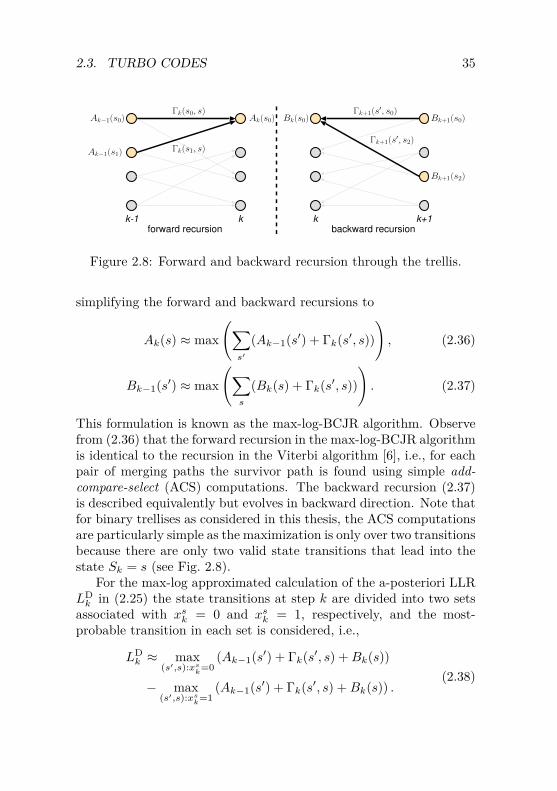
2.3. TURBO CODES 35
Ak−1(s0)
Ak−1(s1)
Ak(s0)Γk(s0, s)
Bk+1(s0)
Bk+1(s2)
Bk(s0)
forward recursion backward recursion
Γk+1(s′, s0)
Γk+1(s′, s2)
kk-1
Γk(s1, s)
k+1k
Figure 2.8: Forward and backward recursion through the trellis.
simplifying the forward and backward recursions to
Ak(s) ≈ max(∑
s′
(Ak−1(s′) + Γk(s′, s))), (2.36)
Bk−1(s′) ≈ max(∑
s
(Bk(s) + Γk(s′, s))). (2.37)
This formulation is known as the max-log-BCJR algorithm. Observefrom (2.36) that the forward recursion in the max-log-BCJR algorithmis identical to the recursion in the Viterbi algorithm [6], i.e., for eachpair of merging paths the survivor path is found using simple add-compare-select (ACS) computations. The backward recursion (2.37)is described equivalently but evolves in backward direction. Note thatfor binary trellises as considered in this thesis, the ACS computationsare particularly simple as the maximization is only over two transitionsbecause there are only two valid state transitions that lead into thestate Sk = s (see Fig. 2.8).
For the max-log approximated calculation of the a-posteriori LLRLDk in (2.25) the state transitions at step k are divided into two sets
associated with xsk = 0 and xsk = 1, respectively, and the most-probable transition in each set is considered, i.e.,
LDk ≈ max
(s′,s):xsk=0
(Ak−1(s′) + Γk(s′, s) +Bk(s))
− max(s′,s):xs
k=1
(Ak−1(s′) + Γk(s′, s) +Bk(s)) .(2.38)
36 CHAPTER 2. PRELIMINARIES
This means that the final LLRs are also calculated using simple ACSoperations. In contrast to the two recursions, however, the calcula-tions are more involved as they require maximization over more thantwo state transitions.
The branch metrics Γk(s′, s) can be calculated from (2.32). Notethat constant terms in the branch metrics can be safely omitted duringdecoding because only differences are considered in the computationsof the state metrics and the a-posteriori LLRs. Neglecting constantterms, it follows that
Γk(s′, s) ≈ 12µ
sk(s′, s)(Ls
k + LAk ) + 1
2µpk(s′, s)Lp
k. (2.39)
Hence, for the considered binary convolutional code, there are fourpossible branch metrics per trellis step k and each branch metricis a combination of the sum Ls
k + LAk and Lp
k. In practice, thebranch metrics are typically further simplified by adding the term(1/2)(Ls
k + LAk ) + (1/2)Lp
k to all branch metrics, resulting in the fourvalues Γk,1 = 0, Γk,2 = Ls
k + LAk , Γk,3 = Lp
k, and Γk,4 = Γk,2 + Γk,3.Due to its simple operations, the max-log-BCJR algorithm is highly
suitable for VLSI implementation. However, it was shown that themax-log approximation provides in general too optimistic extrinsicLLR values [46], leading to a considerable performance degradation.This performance loss can be mitigated to a large extent by employingextrinsic scaling [46], i.e., by scaling the extrinsic LLRs LE
k in (2.23)and (2.24) with a constant factor sE smaller than 1.
2.3.4 The Soft-Output Viterbi AlgorithmThe SOVA [41] consists of two parts. The first part is identical tothe conventional hard-output Viterbi algorithm [6] and amounts to aforward recursion through the trellis of the convolutional code followedby a trace-back that delivers the most probable path, i.e., the MLpath (and thus the most probable sequence of xs
k). In the secondpart, the SOVA generates soft-information in the form of estimatesLDk of the a-posteriori LLRs in (2.22) based on the extracted ML path.
Note that this approach is in strong contrast to the BCJR algorithm,which generates exact a-posteriori LLRs by considering all possible
2.3. TURBO CODES 37
paths through the trellis. The SOVA is roughly half as complex asthe max-log-BCJR algorithm [42].
Computation of ML Path
The SOVA first traces the trellis in forward direction. This forwardrecursion is identical to the one in the Viterbi algorithm [6] andcan be expressed as in (2.36), where the branch metrics Γk(s′, s)are identical to the ones in (2.39). In particular, the SOVA re-cursively selects for each state s ∈ S in trellis step k one of thetwo possible candidate state metrics Mk,1(s) = Ak−1(s′) + Γk(s′, s)and Mk,2(s) = Ak−1(s′′) + Γk(s′′, s) (where s′ and s′′ are the twopredecessor states of s) according to Ak(s) = max(Mk,1(s),Mk,2(s)).While doing so, it stores for each state the respective decision bit dk(s)that is associated with the selected branch. In addition, it also storesthe difference magnitudes of the candidate state metrics
∆k(s) = |Mk,1(s)−Mk,2(s)|. (2.40)
During trace-back, the SOVA determines the ML path and providesthe corresponding states sk and decision bits dk along this path. Notethat dk correspond to the hard-outputs xs
k = bk provided by theconventional Viterbi algorithm. We denote the difference magnitudesalong the extracted ML path as ∆k. The difference magnitudes anddecision bits along the concurrent path merging into the ML path attrellis step k are referred to as ∆c
k−l and dck−l, respectively. Theseparameters are illustrated in Fig. 2.9.
Computation of Soft-Information
Consider the determined ML path at trellis step k passing throughstate sk. We refer to the ML path up to step k as sk. The corre-sponding concurrent path at step k that was discarded during theforward recursion is denoted as sc
k (see Fig. 2.9). The computationof the soft-information starts by noticing that the probability that awrong decision was made by selecting sk and discarding sc
k dependson the magnitude difference ∆k as [41,45]
Pr[sk is wrong] = psk= 1
1 + exp(∆k) . (2.41)
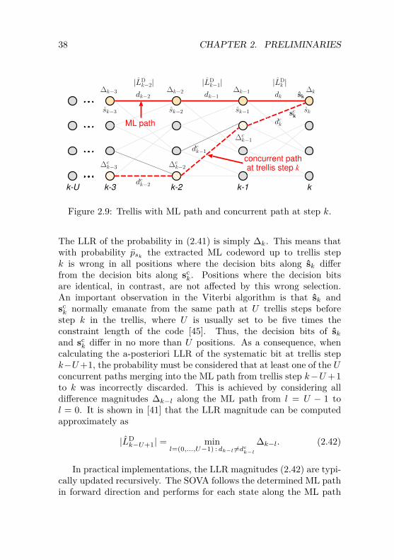
38 CHAPTER 2. PRELIMINARIES
kk-1k-2k-3
ML path
∆kdk∆k−1
∆ck−1
sk−1
dck
dck−1
dk−1∆k−2dk−2
|LDk−2|
∆k−3
concurrent pathat trellis step k∆c
k−2
sk−2sk−3
∆ck−3
dck−2k-U
sk
|LDk−1| |LD
k |sk
sck
Figure 2.9: Trellis with ML path and concurrent path at step k.
The LLR of the probability in (2.41) is simply ∆k. This means thatwith probability psk
the extracted ML codeword up to trellis stepk is wrong in all positions where the decision bits along sk differfrom the decision bits along sc
k. Positions where the decision bitsare identical, in contrast, are not affected by this wrong selection.An important observation in the Viterbi algorithm is that sk andsck normally emanate from the same path at U trellis steps before
step k in the trellis, where U is usually set to be five times theconstraint length of the code [45]. Thus, the decision bits of skand sc
k differ in no more than U positions. As a consequence, whencalculating the a-posteriori LLR of the systematic bit at trellis stepk−U+1, the probability must be considered that at least one of the Uconcurrent paths merging into the ML path from trellis step k−U+1to k was incorrectly discarded. This is achieved by considering alldifference magnitudes ∆k−l along the ML path from l = U − 1 tol = 0. It is shown in [41] that the LLR magnitude can be computedapproximately as
|LDk−U+1| = min
l=(0,...,U−1) : dk−l 6=dck−l
∆k−l. (2.42)
In practical implementations, the LLR magnitudes (2.42) are typi-cally updated recursively. The SOVA follows the determined ML pathin forward direction and performs for each state along the ML path
2.3. TURBO CODES 39
an U -step trace-back of the merging concurrent path (see Fig. 2.9).During the trace-back at state sk, it updates the related U LLRmagnitudes according to
|LDk−l| ← min(∆k, |LD
k−l|) if dk−l 6= dck−l, ∀l ∈ [0, U − 1], (2.43)
where all magnitudes |LDk | are initialized with infinity prior to de-
coding. Hence, each LLR magnitude is updated at most U timesduring U consecutive trace-backs. Finally, the LLR magnitude |LD
k |is combined with the sign associated with the ML decision dk to yieldthe output LD
k . The parameter U is typically referred to as updatewindow.
Improved SOVA Note that the original update rule in (2.43) doesnot improve the estimate of |LD
k−l| when dk−l = dck−l. Several modifi-cations of the original SOVA have been proposed to account for thismajor shortcoming (e.g., [43, 44]). A particular simple yet effectivemodification is the one proposed in [44], which considers in additionto the difference magnitudes ∆k along the ML path also the differencemagnitudes ∆c
k−l along the concurrent merging paths (see Fig. 2.9).These additional ∆c
k−l improve the reliability of the a-posteriori LLRwhen dk−l = dck−l according to
|LDk−l| ← min(∆k + ∆c
k−l, |LDk−l|) if dk−l = dck−l, ∀l ∈ [1, U1 − 1],
(2.44)
where we choose U1 ≤ U . This second update rule complements thefirst original update rule in (2.43).
It was shown in [47] that, similar to the max-log-BCJR algorithm,the quality of the extrinsic LLR values provided by the SOVA can beimproved by scaling the extrinsic a-posteriori LLR values LE
k in (2.23)and (2.24) with a constant factor sE smaller than 1.
2.3.5 Error-Rate Performance ComparisonIn order to characterize the BER performance of the discussed turbodecoding algorithms, the 3GPP turbo code with the block interleaverspecified for UMTS (see [38]) is considered. The simulations have
40 CHAPTER 2. PRELIMINARIES
been performed without puncturing (i.e., R = RTC = 1/3) for blocklength K = 5114 over an AWGN channel as described in Sec. 2.1.
Fig. 2.10(a) shows the BER performance of the turbo decoder withoptimal exact BCJR SISO decoding algorithm for different iterationsI. Observe that for this specific turbo code the BER starts saturatingafter roughly 15 to 20 iterations. In practice, however, 5 to 8 iterationsare typically performed by corresponding hardware implementations.
In Fig. 2.10(b), the performance of the exact BCJR algorithmis compared with the performance of the max-log-BCJR and thesoft-output Viterbi algorithms at I = 8 iterations (i.e., Ih = 16half-iterations). Considering first the max-log-BCJR algorithm, itcan be observed that the straightforward application of the max-logapproximation leads to a strong performance degradation of 0.4 dB.This degradation can be mitigated to a large extent by using extrinsicscaling. In fact, with an optimized scaling factor of sE = 0.6875, theperformance of the max-log-BCJR algorithm is improved by 0.3 dB,closing the gap to the optimal BCJR algorithm to less than 0.1 dB.Next consider the SOVA SISO decoding algorithm in Fig. 2.10(b).Simulations have shown that for the considered unpunctured turbocode the length U of the update window must be chosen larger than20 trellis steps in order to avoid serious performance degradation.In the presented simulations we use U = 25. It can be seen thatthe original SOVA with the single original update rule in (2.43) andoptimized extrinsic scaling factor sE = 0.7188 exhibits a significantlyworse performance than the max-log-BCJR algorithm. Due to thisreason, the SOVA has been considered only marginally in practicalturbo decoder implementations. However, by employing the secondupdate rule in (2.44) with U1 = U = 25, the performance of theSOVA improves substantially and the performance gap compared tothe max-log-BCJR algorithm shrinks to 0.1 dB.
2.4 SummaryIn this chapter, the basics of LDPC and turbo codes have been re-viewed. It has has been shown that virtually all wireless standardsthat employ LDPC codes consider the structured class of quasi-cyclicLDPC codes. In order to tune both block length and code rate of
2.4. SUMMARY 41
these codes, wireless standards typically foresee a range of parity-checkmatrices that are scheduled according to the present transmissionenvironment. With respect to the considered 3GPP turbo codes, wehave seen that the specified interleavers enable a wide range of blocklengths, and that the code rate is tuned by puncturing the code atthe output of the encoder from the inherent code rate RTC = 1/3 tohigher code rates (which can be close to 1).
Furthermore, best-practice of LDPC and turbo decoding algo-rithms have been summarized. Practical QC-LDPC decoders performmessage-passing on the parity-check constrained factor graph of thecode and employ low-complexity message update rules that reducethe VLSI implementation costs compared to the optimal sum-productalgorithm at the expense of a small error-rate performance loss. Aparticular favorable decoding algorithm for practical implementationsis the offset-min-sum algorithm combined with the layered schedule,which is focused on in the remainder of this thesis.
Practical turbo decoders typically operate on the trellis constrainedfactor graph of the code and rely on the max-log-BCJR SISO decodingalgorithm to decode the component convolutional codes. This SISOdecoding algorithm provides a significant reduction of implementationcomplexity compared to the optimal BCJR algorithm at the expenseof a negligible error-rate performance loss — when combined withextrinsic scaling. Although the soft-output Viterbi algorithm comeswith halved complexity compared to the max-log-BCJR algorithm, ithas been considered only marginally for SISO decoding in practicalturbo decoder implementations due to its sub-optimal performance.However, we have described an improved SOVA, which shows a per-formance close to the one of the max-log-BCJR algorithm, renderingthe SOVA a competitive alternative.
The efficient VLSI implementation of these low-complexity decod-ing algorithms under the outlined flexibility requirements is the focusof the following two chapters.
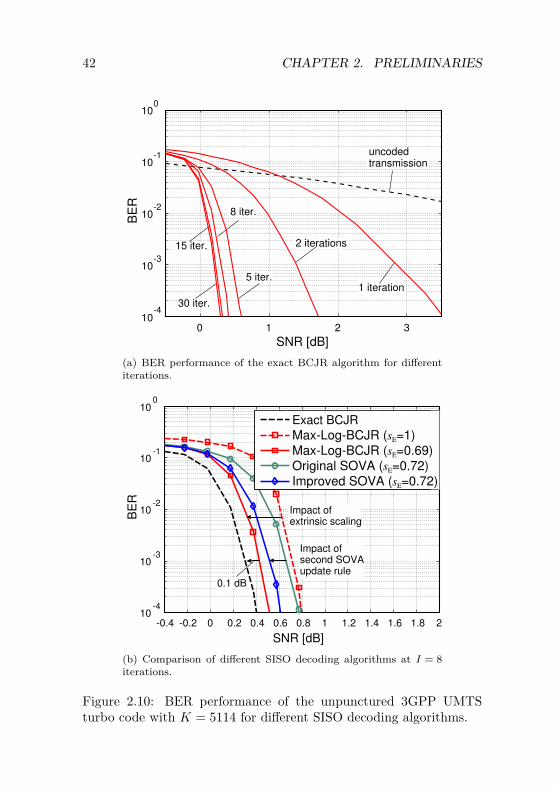
42 CHAPTER 2. PRELIMINARIES
0 1 2 310
-4
10-3
10-2
10-1
100
BE
R
SNR [dB]
uncodedtransmission
1 iteration
2 iterations
5 iter.
8 iter.
15 iter.
30 iter.
(a) BER performance of the exact BCJR algorithm for differentiterations.
-0.4 -0.2 0 0.2 0.4 0.6 0.8 1 1.2 1.4 1.6 1.8 210
-4
10-3
10-2
10-1
100
BE
R
Exact BCJR
Max-Log-BCJR (sE=1)
Max-Log-BCJR (sE=0.69)
Original SOVA (sE=0.72)
Improved SOVA (sE=0.72)
SNR [dB]
Impact ofextrinsic scaling
Impact ofsecond SOVAupdate rule
0.1 dB
(b) Comparison of different SISO decoding algorithms at I = 8iterations.
Figure 2.10: BER performance of the unpunctured 3GPP UMTSturbo code with K = 5114 for different SISO decoding algorithms.
Chapter 3
VLSI Implementation ofLDPC Decoding
This chapter is concerned with the energy-efficient VLSI implemen-tation of flexible QC-LDPC decoders. In Sec. 3.1 we first present ahigh-level architecture exploration with reference to designs from theopen literature, where the LDPC decoder design space is partitionedinto three different architecture classes. We describe similarities anddifferences between these architecture classes and identify the classthat is in general most suitable for flexible QC-LDPC decoder im-plementation. Based on this architecture class, a specific efficientflexible QC-LDPC decoder architecture is presented in Sec. 3.2. Thesecond part of this chapter then deals with the energy-efficient imple-mentation of the presented architecture and provides correspondingimplementation results.
3.1 High-Level Architecture ExplorationFrom a high-level perspective, virtually all implementations of message-passing LDPC decoders found in the open literature are derived froman isomorphic architecture [18] which is a direct mapping of the parity-check constrained factor graph in Fig. 2.2 to three types of hardwarecomponents: i) VN units (VNUs) and CN units (CNUs) to compute
43
44 CHAPTER 3. IMPLEMENTATION OF LDPC DECODING
the update equations, ii) an interconnect network representing theedges of the graph, and iii) storage devices for the L-values andmessages. Starting from this prototype architecture, different imple-mentation trade-offs are obtained through architectural transforma-tions such as resource sharing across VNUs and CNUs and iterativedecomposition of the update equations.
In what follows, it is illustrated how the design space can be parti-tioned into three different architecture classes [22]: Full-parallel, row-parallel, and block-parallel. These three classes are depicted in Fig. 3.1.In order to evaluate the general impact of these architectural choiceson silicon area and energy efficiency, data points from LDPC decoderimplementations found in the open literature are collected and putinto relation in Fig. 3.2. For a fair comparison, technology scalingis taken into account, i.e., we scale the core area, throughput, andenergy efficiency of all designs to the 90 nm CMOS technology nodewith 1.0 V supply voltage. We assume 5 and 10 iterations for designsbased on layered (filled markers) and flooding schedules, respectively,to account for the difference in convergence speed. Fig. 3.2(a) relatesthe area per bit to the time required for decoding. The diagonallines correspond to constant silicon efficiency. Fig. 3.2(b) relates theenergy efficiency in terms of energy per bit to the maximum achiev-able throughput for each design. The diagonals in this figure corre-spond to constant power consumption. Note that area and energy inboth figures are normalized by the codeword length N and that thethroughput is measured at the input of the decoder (i.e., in terms ofcodeword bits per second) in order to avoid dependencies on the coderate. The considered energy efficiency is thus in energy per codewordbit, which is the energy efficiency measure that is typically reportedin LDPC decoder publications.1
1In order to convert energy per codeword bit to energy per information bit, onecan simply divide the first measure by the code rate.
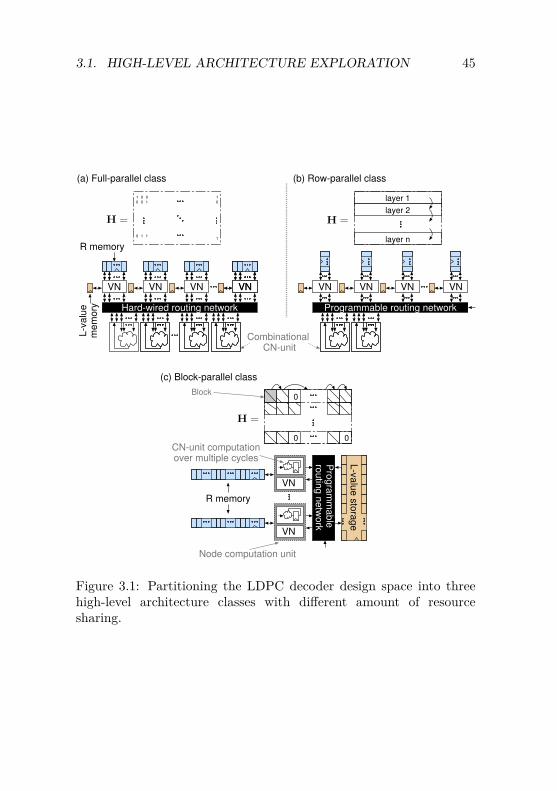
3.1. HIGH-LEVEL ARCHITECTURE EXPLORATION 45
1 0 0
0 0 1
0 1 1
1
0
1
layer 1
Block0
0 0
Combinational CN-unit
Hard-wired routing network
VN
Programmable routing network
VN VN VN VN
VN
Pro
gra
mm
able
ro
utin
g n
etw
ork
VN
L-v
alu
e s
tora
ge
R memory
CN-unit computationover multiple cycles
layer 2
layer n
H =
H =H =
VN VN VN VN
(c) Block-parallel class
(b) Row-parallel class(a) Full-parallel class
R memory
L-v
alu
em
em
ory
Node computation unit
Figure 3.1: Partitioning the LDPC decoder design space into threehigh-level architecture classes with different amount of resourcesharing.
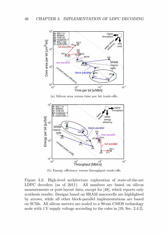
46 CHAPTER 3. IMPLEMENTATION OF LDPC DECODING
10-5
10-4
10-3
10-2
102
103
104
105
[51]
[60]
[58]
[63]
[49]
[57] [59]
[61]
[50] [52]-a [55]
[54]
[15]
[21]
[62]
[64]
full-parallel
row-parallel
block-parallel
Core
are
a p
er
bit [um
2/b
it]
constant silicon efficiency
bette
r silic
on
effic
ienc
y
higherthroughput
lessarea
Time per bit [s/Mbit]
[52]-b
SRAMmacro-cells
10GBASE-T
WiMAX802.11n
DVB-S2
CUSTOM802.11ad
[48]
(a) Silicon area versus time per bit trade-offs.
102
103
104
105
101
102
103
104
[51]
[60]
[58]
[63]
[49]
[57]
[59]
[61]
[50]
[52]-a
[55]
[15] [21]
[62]
full-parallel
row-parallel
block-parallel
constant power [mW
]
Throughput [Mbit/s]
Energ
y p
er
bit [pJ/b
it] better
energyefficiency
higherthroughput
lower
power
10GBASE-TWiMAX802.11nDVB-S2CUSTOM
[52]-b
SRAMmacro-
cells
10GBASE-T
WiMAX802.11n
DVB-S2
CUSTOM
(b) Energy efficiency versus throughput trade-offs.
Figure 3.2: High-level architecture exploration of state-of-the-artLDPC decoders (as of 2011). All numbers are based on siliconmeasurements or post-layout data, except for [48], which reports onlysynthesis results. Designs based on SRAM macrocells are highlightedby arrows, while all other block-parallel implementations are basedon SCMs. All silicon metrics are scaled to a 90 nm CMOS technologynode with 1 V supply voltage according to the rules in [19, Sec. 2.4.2].
3.1. HIGH-LEVEL ARCHITECTURE EXPLORATION 47
3.1.1 Full-Parallel Architecture
Full-parallel LDPC decoder designs, e.g., [49–52], were among thefirst implementations of LDPC decoders. Corresponding implemen-tations inherently rely on the flooding schedule and directly imple-ment the isomorphic architecture of the message-passing algorithm.A high-level block-diagram of a typical full-parallel design is shownin Fig. 3.1(a). The update equations are mapped into individualVNUs and CNUs that exchange messages through a hard-wired routingnetwork. The parallel processing allows each iteration to be performedin a single clock cycle, in which VNUs fetch all R-messages from local(register based) storage and compute new Q-messages that are sentthrough the routing network. The CNUs compute new R-messagesand send them back to the VNUs where they are stored for the nextiteration and are used to update the local L-value registers.
Discussion
The main advantage of the full-parallel architecture is the ability tofully exploit the intrinsic parallelism offered by LDPC codes. Thisarchitecture enables very high throughput since one iteration is per-formed per clock cycle with simple computations that allow for highoperating clock frequencies. This performance advantage is visiblein Fig. 3.2(a), where the designs based on this isomorphic architec-ture achieve highest throughput of tens of Gbps. Unfortunately, thecomplex routing network that connects CNUs and VNUs turns outto be a major implementation bottleneck for these designs [52] andstraightforward implementations exhibit extremely poor area utiliza-tion and suffer from a considerable speed penalty that may evenbecome worse when proceeding to more advanced CMOS technologynodes. Proposals to mitigate this routing bottleneck include the seri-alization of multi-bit interconnect buses [50] or guided placement toreduce the number or the length of global wires [53]. A particularlyinteresting approach is a modification on the algorithmic level thatreduces the amount of routing at the expense of a small error-rate per-formance degradation [52]. The positive impact of this modificationon silicon area and energy efficiency is clearly visible from Fig. 3.2(a)and Fig. 3.2(b), where the design with the modified algorithm [52]-(a)
48 CHAPTER 3. IMPLEMENTATION OF LDPC DECODING
achieves much better implementation results than the accompanyingreference design without algorithm modifications [52]-(b).
Application to flexible QC-LDPC decoders Full-parallel ar-chitectures have been considered mainly for wireline communicationstandards, such as, e.g., 10GBASE-T 10 Gbps Ethernet, due to thevery high throughput provided by this architecture class. Since thefull-parallel architecture represents the direct hardware mapping of aspecific parity-check matrix, this class cannot provide any flexibility.Therefore, it is generally ill-suited for wireless communication stan-dards that require the support for different parity-check matrices inorder to tune code rate and block length.
3.1.2 Row-Parallel ArchitectureThe row-parallel architecture class, e.g., [15, 48, 54, 55], is a step to-wards less parallelism by means of resource sharing [18] among theCNUs. The main objective is to reduce active silicon area and topartially alleviate the routing bottleneck while maintaining very highthroughput. The principle underlying row-parallel architectures isillustrated in Fig. 3.1(b). Essentially, the parity-check matrix is par-titioned vertically into layers. The parity-check equations in eachlayer are executed in parallel on a set of time-shared CNUs. Aniteration now consists of multiple cycles in which the VNUs accessthe R-messages corresponding to the current layer sequentially froma small storage array (typically too small for economic use of SRAMmacrocells) to compute the Q-messages and communicate them tothe CNUs through a programmable routing network. The complex-ity and the amount of bits required to control this programmablerouting network heavily depend on the structure of the code andon its partitioning into layers. In the worst-case, a full crossbar isneeded to realize the interconnect network. Due to the sequentialprocessing of the CNUs, the update of the L-values in the VNUscan be performed in an iteratively decomposed fashion2, while the
2The degree of iterative decomposition depends on the choice of the layers andon the code. Ideally, the layers can be selected according to (2.12), where thedegree of each column of a layer is one.
3.1. HIGH-LEVEL ARCHITECTURE EXPLORATION 49
computation of R-messages in the CNUs is still carried out in a singlecycle on a purely combinational network.
Discussion
Considering the reference designs in Fig. 3.2(a), it is interesting to seethat row-parallel architectures are still sufficiently fast to meet eventhe 10 Gbps of high-throughput wireline communication standards(e.g., 10GBASE-T). At the same time, they provide an area advantageover full-parallel designs, which is partially due to a smaller numberof global wires and CNUs and partially due to architectural/layoutmeasures that exploit regularities in the code [55] or circuit-level mea-sures that reuse routing resources [15]. A key advantage of the row-parallel architecture is that it is naturally suited to support the layeredschedule, which allows for fewer iterations. Note that additionalstorage to hold the L-values computed in the previous iteration, whileprocessing layers of the current iteration, can be avoided for a layeredschedule with proper layer selection as in (2.12). This difference inarea is visible in Fig. 3.2(a) when comparing the designs [55] and [15].
Application to flexible QC-LDPC decoders In general, theprogrammable routing network illustrated in Fig. 3.1(b) required bythe row-parallel architecture class provides the flexibility to supportmultiple parity-check matrices with a single decoder. For this rea-son, this architecture class has been recently considered in severalflexible QC-LDPC decoders tailored to the emerging high-throughputwireless standards IEEE 802.11ad and IEEE 802.15.3c (e.g., [48,56]).Although the structure of QC-LDPC codes significantly reduces thecomplexity of the programmable routing network compared to a fullcrossbar, the economic implementation of such networks in conjunc-tion with the parallel execution of full parity-check equations stillrepresents a major design challenge.
3.1.3 Block-Parallel ArchitectureBlock-parallel designs (e.g., [21,57–64]) rely on further resource shar-ing and further iterative decomposition. Fig. 3.1(c) outlines the ar-chitectural principle, which is usually used in combination with the
50 CHAPTER 3. IMPLEMENTATION OF LDPC DECODING
layered message-passing schedule. In essence, this architecture class isobtained by starting from the row-parallel approach and by partition-ing the computation of a layer further into multiple cycles, correspond-ing to multiple blocks in the parity-check matrix. Per clock cycle, asingle block, multiple blocks or only a part of a block can be processed.This iterative decomposition simplifies the CN processing and allowsfor resource sharing also across the VNUs. Typically, the VNUsare now tightly coupled to the CNUs to form a node computationunit (NCU). Due to the reduced parallel access requirements com-pared to the other two architecture types3, R-messages and L-valuescan now be stored in area-efficient SRAM macrocells. However, aprogrammable routing network is required that connects the L-valuestorage array to the NCUs since in each block a different NCU isassociated with a particular L-value.
Discussion
Fig. 3.2(a) clearly illustrates how the block-parallel designs cover thelower-throughput region of the design space, but it also shows thatmore recent designs are approaching the multiple-Gbps range [61,64].This is achieved by increasing the number of blocks that are processedin parallel, either within a layer or across layers. The trajectory acrossthe designs [62], [61], [64] illustrates that this transition is possibleat an almost constant silicon efficiency, which reveals the suitabil-ity of the block-parallel architecture class to provide very differentarea/throughput trade-offs that can be tailored to the application athand.
In terms of energy efficiency, Fig. 3.2(b) reveals a small disad-vantage of the block-parallel designs compared to the full-paralleland row-parallel designs. This trend can be explained by the higherdegree of control required after extensive resource sharing and itera-tive decomposition. Another trend visible from Fig. 3.2 is the splitbetween two types of block-parallel designs. The first type exploitsthe ability of the architecture to use area-efficient SRAM macrocells.
3The parallel access requirements of the block-parallel architecture class arereduced compared to the full-parallel and row-parallel classes, but they still posea significant challenge for the implementation of block-parallel QC-LDPC decodersas shown in Sec. 3.2.
3.1. HIGH-LEVEL ARCHITECTURE EXPLORATION 51
The second type relies on latch or flip-flop based RAMs synthesizedfrom standard-cell libraries, which we will refer to as standard-cellbased memories (SCMs).
Application to flexible QC-LDPC decoders The block-basedprocessing in conjunction with structured codes significantly facili-tates reconfigurability. Due to this reason, this architecture classhas been widely employed for flexible decoder implementations. ForQC-LDPC codes, the programmable interconnect can be realized par-ticularly efficiently when the blocks processed by the block-parallelarchitecture coincide with the elements of the QC matrix prototypeHp in (2.7). In this case, the programmable interconnect can be imple-mented using an area-efficient programmable cyclic shifter (CS) [62]that is controlled by the related shift amounts cmp,np
in Hp.
3.1.4 Conclusions
It has been shown that the design space of LDPC decoders can bepartitioned into three architecture classes. Practical full-parallel de-signs achieve very high throughput in excess of 10 Gbps but cannotprovide any flexibility in terms of code rate or block length. Therow-parallel and block-parallel designs reduce the silicon area com-pared to the full-parallel designs with different degrees of resourcesharing and iterative decomposition at the expense of a degradationin throughput. While both architecture classes offer flexibility, theblock-parallel class is especially suitable for QC-LDPC codes as itnaturally fits together with the block structure of these codes. It hasbeen shown that this architecture class is highly scalable and supportsthe full range of throughput requirements found in modern wirelessstandards, including multiple-Gbps as required by emerging systems.The latter is achieved by processing multiple blocks in parallel, whichenables throughput close to the one of row-parallel designs at lowersilicon area (compare designs [64] and [48] in Fig. 3.2(a)). Due to thesefavorable properties, the block-parallel architecture class is consideredin the remainder of this thesis.
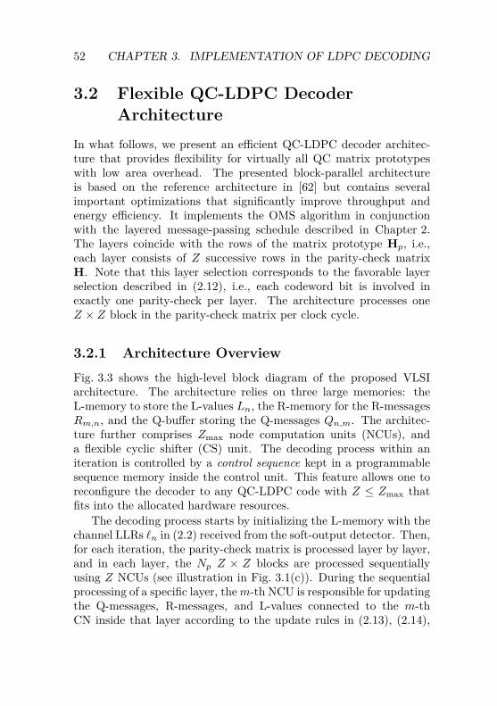
52 CHAPTER 3. IMPLEMENTATION OF LDPC DECODING
3.2 Flexible QC-LDPC DecoderArchitecture
In what follows, we present an efficient QC-LDPC decoder architec-ture that provides flexibility for virtually all QC matrix prototypeswith low area overhead. The presented block-parallel architectureis based on the reference architecture in [62] but contains severalimportant optimizations that significantly improve throughput andenergy efficiency. It implements the OMS algorithm in conjunctionwith the layered message-passing schedule described in Chapter 2.The layers coincide with the rows of the matrix prototype Hp, i.e.,each layer consists of Z successive rows in the parity-check matrixH. Note that this layer selection corresponds to the favorable layerselection described in (2.12), i.e., each codeword bit is involved inexactly one parity-check per layer. The architecture processes oneZ × Z block in the parity-check matrix per clock cycle.
3.2.1 Architecture Overview
Fig. 3.3 shows the high-level block diagram of the proposed VLSIarchitecture. The architecture relies on three large memories: theL-memory to store the L-values Ln, the R-memory for the R-messagesRm,n, and the Q-buffer storing the Q-messages Qn,m. The architec-ture further comprises Zmax node computation units (NCUs), anda flexible cyclic shifter (CS) unit. The decoding process within aniteration is controlled by a control sequence kept in a programmablesequence memory inside the control unit. This feature allows one toreconfigure the decoder to any QC-LDPC code with Z ≤ Zmax thatfits into the allocated hardware resources.
The decoding process starts by initializing the L-memory with thechannel LLRs `n in (2.2) received from the soft-output detector. Then,for each iteration, the parity-check matrix is processed layer by layer,and in each layer, the Np Z × Z blocks are processed sequentiallyusing Z NCUs (see illustration in Fig. 3.1(c)). During the sequentialprocessing of a specific layer, them-th NCU is responsible for updatingthe Q-messages, R-messages, and L-values connected to the m-thCN inside that layer according to the update rules in (2.13), (2.14),
3.2. QC-LDPC DECODER ARCHITECTURE 53
Cyclic shifter unit
L-memory
Se
qu
en
ce
me
mo
ryC
ontr
ol unit
bk
MIN SEL
NCU 1
MIN SEL
NCU Zmax Q
-buffer
R-memory
NCU pool
Zmax Lold
Zmax Lnew
Zmax Rnew
Zmax Rold
Zmax Qnew
Zmax Qnew
ℓn
Figure 3.3: High-level block diagram of the QC-LDPC decoderarchitecture.
and (2.15). One block is processed per clock cycle, and for eachprocessed block the associated Z L-values are fetched from the L-memory and cyclically left-shifted by the CS unit in order to provideeach NCU with the proper L-value according to the correspondingshift amount in the matrix prototype. The Z L-values are writtenback to the L-memory after being updated in the NCUs.
Note that only blocks with shift amount cmp,np6=∞ have to be
considered during decoding. The blocks with cmp,np=∞, in contrast,
do not contribute to the message updates since they are all-zeroblocks (see Sec. 2.2.1). Thus, these blocks can safely be skipped byour architecture. We emphasize that for Z < Zmax only a subset of the
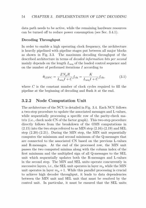
54 CHAPTER 3. IMPLEMENTATION OF LDPC DECODING
data path needs to be active, while the remaining hardware resourcescan be turned off to reduce power consumption (see Sec. 3.4.1).
Decoding Throughput
In order to enable a high operating clock frequency, the architectureis heavily pipelined with pipeline stages put between all major blocksas shown in Fig. 3.3. The maximum decoding throughput of thedescribed architecture in terms of decoded information bits per secondmainly depends on the length Lseq of the loaded control sequence andon the number of performed iterations I according to
θLDPC = ZNpR
LseqI + Cfclk = K
LseqI + Cfclk, (3.1)
where C is the constant number of clock cycles required to fill thepipeline at the beginning of decoding and flush it at the end.
3.2.2 Node Computation UnitThe architecture of the NCU is detailed in Fig. 3.4. Each NCU followsa two-step procedure to update the associated messages and L-values,while sequentially processing a specific row of the parity-check ma-trix (i.e., check node CN of the factor graph). This two-step proceduredirectly follows from the breakdown of the OMS computations in(2.15) into the two steps referred to as MIN step (2.16)-(2.19) and SELstep (2.20)-(2.21). During the MIN step, the MIN unit sequentiallycomputes the minimum and second minimum of the Q-messages thatare connected to the associated CN based on the previous L-valuesand R-messages. At the end of the processed row, the MIN unitpasses the two computed minima along with the column index of thefirst minimum and the multiplied sign of all Q-messages to the SELunit which sequentially updates both the R-messages and L-valuesin the second step. The MIN and SEL units operate concurrently insuccessive layers, i.e., the SEL unit operates in layer mp while the MINunit operates in layer mp + 1. While this parallel processing is crucialto achieve high decoder throughput, it leads to data dependenciesbetween the MIN unit and SEL unit that must be resolved by thecontrol unit. In particular, it must be ensured that the SEL units
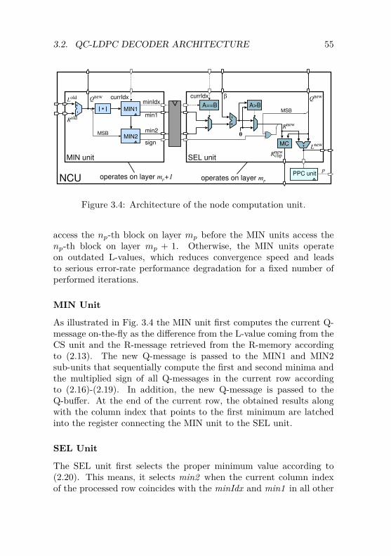
3.2. QC-LDPC DECODER ARCHITECTURE 55
MIN2
MIN1A==B
MC
PPC unit
minIdx
min1
min2
MIN unit SEL unit
NCU
βcurrIdx currIdx
p
Lnew
Rnew
0
sign
Lold
Rold
Qnew
Qnew
Rnewclip
A>B
MSB
MSB
operates on layer mp+1 operates on layer m
p
Figure 3.4: Architecture of the node computation unit.
access the np-th block on layer mp before the MIN units access thenp-th block on layer mp + 1. Otherwise, the MIN units operateon outdated L-values, which reduces convergence speed and leadsto serious error-rate performance degradation for a fixed number ofperformed iterations.
MIN Unit
As illustrated in Fig. 3.4 the MIN unit first computes the current Q-message on-the-fly as the difference from the L-value coming from theCS unit and the R-message retrieved from the R-memory accordingto (2.13). The new Q-message is passed to the MIN1 and MIN2sub-units that sequentially compute the first and second minima andthe multiplied sign of all Q-messages in the current row accordingto (2.16)-(2.19). In addition, the new Q-message is passed to theQ-buffer. At the end of the current row, the obtained results alongwith the column index that points to the first minimum are latchedinto the register connecting the MIN unit to the SEL unit.
SEL Unit
The SEL unit first selects the proper minimum value according to(2.20). This means, it selects min2 when the current column indexof the processed row coincides with the minIdx and min1 in all other
56 CHAPTER 3. IMPLEMENTATION OF LDPC DECODING
cases. Then, the OMS specific offset β is subtracted from the selectedminimum. The magnitude of the new R-message is obtained by asimple max-function as in (2.21). The sign of the new R-messagecorresponds to the overall product of all Q-message signs receivedfrom the MIN unit (see Fig. 3.4) with the sign of the current Q-message (retrieved from the Q-buffer) being excluded by a simpleXOR operation. The new L-value is computed by adding the updatedR-message to the Q-message.
Note that the dynamic range of the L-values can become ratherlarge in general, due to the iterative updates performed on thesevalues. To limit the dynamic range of the L-values, we apply message-clipping to the R-messages as proposed in [62]. In particular, insteadof passing the full R-message to the R-memory, only the part is for-warded which was actually added to the Q-message before saturationof the new L-value occurred, i.e.,
Rnewclip = max (min (Rnew, Lmax −Qnew) ,−Lmax −Qnew) , (3.2)
where Lmax denotes the message-clipping parameter (typically themaximum absolute value of the quantized L-value). It was shownin [62] that message clipping allows one to reduce the wordwidth of thequantized L-values and Q-messages from 7 bit to 5 bit at a slight loss inerror-rate performance of the decoder. Thus, message-clipping offersan interesting trade-off between memory requirements and error-rateperformance.
Partial Parity-Check Unit
The partial parity-check (PPC) unit checks if the associated parity-check equation associated with the currently processed row is satisfied,i.e., if hmx> = 0, where hm represents the currently processed row ofthe parity-check matrix H and x corresponds to the hard-estimatesof the codeword obtained form the signs of the updated L-values. Ifthis is the case, the output of the PPC unit, denoted as p in Fig. 3.4,is set to binary-0 at the end of the current row. Combining the checkbits from all active NCUs by a simple OR-operation results in a per-layer PPC bit that is binary-0 only if all parity-check equations in thecurrent layer are satisfied. If a certain number of consecutive per-layerPPCs are correct, early termination is triggered and the decoding
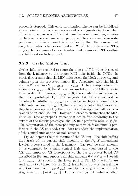
3.2. QC-LDPC DECODER ARCHITECTURE 57
process is stopped. This early termination scheme can be initializedat any point in the decoding process and is configurable in the numberof consecutive per-layer PPCs that must be correct, enabling a trade-off between average number of performed iterations and error-rateperformance. This approach is more flexible than the conventionalearly termination scheme described in [62], which initializes the PPCsonly at the beginning of a new iteration and requires all PPCs withinone full iteration to be correct.
3.2.3 Cyclic Shifter UnitCyclic shifts are required to route the blocks of Z L-values retrievedfrom the L-memory to the proper MIN units inside the NCUs. Inparticular, assume that the MIN units access the block on row mp andcolumn np in the prototype matrix Hp. Associated with this blockare the Z L-values (L(np−1)Z+1, . . . , LnpZ). If the corresponding shiftamount is cmp,np
= 0, the Z L-values are fed to the Z MIN units inlinear order. If, however, cmp,np 6= 0, the circulant construction ofthe matrix prototype Hp in (2.7) suggests that the L-values must becircularly left-shifted by cmp,np
positions before they are passed to theMIN units. As seen in Fig. 3.3, the L-values are not shifted back afterthey have been updated by the SEL units. This approach allows us tosave an additional CS unit. However, in order to ensure that the MINunits still receive proper L-values that are shifted according to theentries of the matrix prototype, the CS unit performs relative shifts.The computation of the corresponding relative shift amounts is per-formed in the CS unit and, thus, does not affect the implementationof the control unit or the control sequence.
Fig. 3.5 depicts the architecture of the CS unit. The shift bufferskeep track of the current shift amounts of the Np Z-dimensionalL-value blocks stored in the L-memory. The relative shift amountc∆ is computed by a small control logic and then passed to theCS. The employed CS corresponds to the barrel-rotator based CSdescribed in [62] and supports all shift amounts 0 ≤ c ≤ Z − 1 for allZ ≤ Zmax. As shown in the lower part of Fig. 3.5, the shifts arerealized by two barrel rotators (BR). Each barrel rotator has a simplestructure based on dlog2(Zmax)e multiplexer stages where the i-thstage (i = 0, . . . , dlog2(Zmax)e−1) executes a cyclic left-shift of either
58 CHAPTER 3. IMPLEMENTATION OF LDPC DECODING
Cyclic shifter unit
Shift buffer 1 Shift buffer 2
Relative
shift amount
Cyclic
shifter
BR 1 BR 2
Shift
control
Z
cc∆
shifted L-values
Zmax L-values
shifted L-values
Z c∆ Zmax L-values
c1
c2
Input
BR 1
BR 2
2 1 2 3Output
2 3 4 1
1 2 3 4
Example:
4 1 2 3
Zmax = 4, Z = 2, c∆ = 1
Figure 3.5: Architecture of the cyclic shifter unit.
zero or 2i positions depending on the shift amount. The two rotatorsreceive two different shift amounts c1 = c∆ and c2 = Zmax − Z + c1,respectively. If Z = Zmax the output of the first rotator corresponds tothe final vector. If Z < Zmax, however, the final vector is assembledfrom the two rotator outputs using a subsequent multiplexer stage.The main advantage of this architecture compared to other approachesfound in the open literature is its low circuit area and fast operation.
3.2.4 Configurable Control UnitThe implemented control unit consists of configuration registers, thesequence memory, and a simple controller. Prior to decoding, theconfiguration registers are configured with the OMS offset β, theparameter Z, and the number of iterations I. In addition, the se-quence memory is loaded with the control sequence which contains theinformation on the current matrix prototype Hp. During decoding,an address counter accesses the sequence memory word by word, andthe individual control words are translated into control signals for thememories, the CS unit, and NCUs. After each iteration, the address
3.2. QC-LDPC DECODER ARCHITECTURE 59
counter is reset. We emphasize that this simple approach enables fullflexibility of the decoder at very low implementation complexity.
Control Sequence
The sequence construction is done off-line. Each sequence containsLseq words comprising Bseq bits. It is obvious from (3.1) that it iscrucial to keep the sequence length as small as possible in order toachieve high decoder throughput. The minimal possible sequencelength L∗seq equals the number of entries in Hp with cm,n 6= ∞,which will be referred to as NB in the following. However, the actualsequence length is typically larger since stall cycles may be requiredto resolve the described data dependencies within the NCUs. Inorder to reduce the number of stall cycles, we exploit the fact thatthe MIN and SEL units generally can process the columns of Hp inarbitrary ordering with the only constraint that the SEL units processthe np-th column on layer mp before the MIN units do so on layermp + 1. Furthermore, our architecture implements a forwarding logicin the L-memory, which provides the possibility to forward updatedL-values coming from the NCUs directly to the CS unit, therebybypassing the L-memory. This technique reduces the latency betweenan L-value is updated in the SEL units and accessed again by the MINunits, which in turn leads to smaller sequence lengths. In addition,it decreases the write access rate of the L-memory and, thus, can beexploited to reduce power consumption by turning off the write logicof the L-memory when bypassing occurs. As an example, Table 3.1shows the sequence lengths of our architecture for all QC-LDPC codesdefined in the IEEE 802.11n standard [33] and compares them tothe corresponding minimal possible sequence lengths L∗seq. It can beobserved that our sequence construction approach in conjunction withthe described memory bypassing yields very efficient sequences witha maximal stall ratio smaller than 5%.
3.2.5 Memory RequirementsAs depicted in Fig. 3.3, the block-parallel processing of our archi-tecture requires the L-memory, R-memory, and Q-buffer to supportan extensively large data bandwidth. In particular, all memories
60 CHAPTER 3. IMPLEMENTATION OF LDPC DECODING
Table 3.1: Sequence lengths Lseq for the IEEE 802.11n standard.Z Code rate Lseq L∗seq Stall ratioa [%]
27
1/2 92 88 4.62/3 88 88 03/4 89 88 1.15/6 91 88 3.4
54
1/2 88 86 2.32/3 88 88 03/4 90 88 2.35/6 86 85 1.2
81
1/2 88 86 2.32/3 88 88 03/4 86 85 1.25/6 80 79 1.3
aThe stall ratio measures the overhead required to resolve the data dependencyin the NCUs. It is defined as (number of stall cycles)/L∗seq.
require one read operation and one concurrent write operation perclock cycle. Due to this reason, all memories must be realized astwo-port4 memories. Furthermore, one address corresponds to Zmaxvalues/messages, where the L-memory and Q-buffer must provideNp addresses and the R-memory NB,max addresses, correspondingto the maximum number of blocks in Hp with cmp,np
6= ∞. Thesememory requirements are summarized in Table 3.2, where BL, BR,and BQ denote the number of bits used to quantize the L-values,R-messages, and Q-messages, respectively. Thus, assuming a typical5 bit quantization for all values and messages and Zmax = 81 asfor the IEEE 802.11n standard [33], each memory has to providea concurrent read and write bandwidth of 405 bit per clock cycle.This large memory access bandwidth in conjunction with the largememory capacities are among the main implementation challenges ofblock-parallel QC-LDPC decoders.
4Two-port memories provide one read and one write access per clock cycle.Single-port memories only provide one write or one read access per clock cycle.
3.3. LOW-POWER MEMORY ARCHITECTURE 61
Table 3.2: Requirements for L-memory, R-memory, and Q-buffer. Allmemories must provide one read and one write access per clock cycle.
L-memory R-memory Q-bufferAddresses Np NB,max NpValues Zmax Zmax Zmaxper address L-values R-messages Q-messagesTotal capacity NpZmaxBL NB,maxZmaxBR NpZmaxBQ
3.3 Low-Power Memory ArchitectureDue to the large parallel read/write memory access requirements inblock-parallel QC-LDPC decoders, the memory components typicallyconsume a dominant share of the total power. For instance, in thereference decoder described in [62], an estimated 68% of total decoderpower is consumed by the memories for L-values and R-messages.Hence, the optimization of the memory components for low power iscrucial when striving for energy-efficient flexible QC-LDPC decoderimplementations.
In general, digital IC designers have two major options for on-chipmemory implementations, namely SRAM macrocells and SCMs.
3.3.1 SRAM Macrocells versus SCMsInterestingly, among the LDPC decoders considered in Fig. 3.2(b),block-parallel decoders based on SCMs generally achieve better en-ergy efficiency than the ones based on SRAM macrocells. This ob-served advantage of SCM based decoders can be attributed to twomain factors [23]: i) SCMs can be more power-efficient than SRAMmacrocells and ii) SCMs can merge with logic blocks, which increasesdata locality and hence may reduce routing overheads and lead toless switching power. SCMs can also be organized in many smallblocks which can be enabled separately. Such a fine-grained memoryorganization is key to reduce power consumption in flexible QC-LDPCdecoders for modes with Z < Zmax. Furthermore, the use of SCMsdescribed in a hardware description language eases the portability of adesign to other technologies. Also, SCMs can be described in a generic
62 CHAPTER 3. IMPLEMENTATION OF LDPC DECODING
way, which simplifies modifications in terms of number of addressesor number of bits per address at design time. SRAM macrocells, onthe other hand, need to be created again for each technology nodeor process design kit, using a dedicated macrocell compiler. Due tothese reasons, we propose to base the memory architecture on SCMs.
A potential drawback of SCMs synthesized from typical commer-cial standard-cell libraries compared to SRAM macrocells is theirlower area efficiency for large memory capacities5. This trend isvisible in Fig. 3.2(a), where it can be seen that block-parallel LDPCdecoders based on SRAM macrocells generally require less silicon areathan the ones based on SCMs. The reason for this is the fact thatcommercial standard-cell libraries typically provide only static latchesand flip-flops which are optimized for high-speed performance andhighest robustness in the context of process-voltage-temperature vari-ations. We emphasize, however, that the area gap of SCMs to SRAMmacrocells can be reduced drastically by relying on custom-designedhigher-density dynamic latches as storage cells (see Sec. 3.4.2).
3.3.2 SCM based Memory ArchitectureAny SCM comprises three building blocks: i) the write logic, ii)the read logic, and iii) the array of storage cells. A comprehensivestudy on the design of SCMs was presented in [23]. In this study, wecompared various architectural choices for the three building blocks toeach other considering different commercial standard-cell libraries anddifferent CMOS technology nodes. According to this study, the mostefficient SCM architecture in terms of power consumption and siliconarea uses a write logic based on clock gates (rather than one based ona conventional enable logic for the storage cells), a read logic basedon simple multiplexers (rather than one based on tri-state buffers),and latches as storage cells. This architecture is used as basis for theL-memory, R-memory, and Q-buffer and is described in more detailin the ensuing discussion. Interestingly, in the application exampleprovided in [23] it was shown that the use of the considered SCMarchitecture reduces the power consumption of an example LDPCdecoder by 37% compared to the use of SRAM macrocells.
5For memory capacities smaller than 1 kbit, the use of commercial SCMs canbe profitable also in terms of silicon area [23].
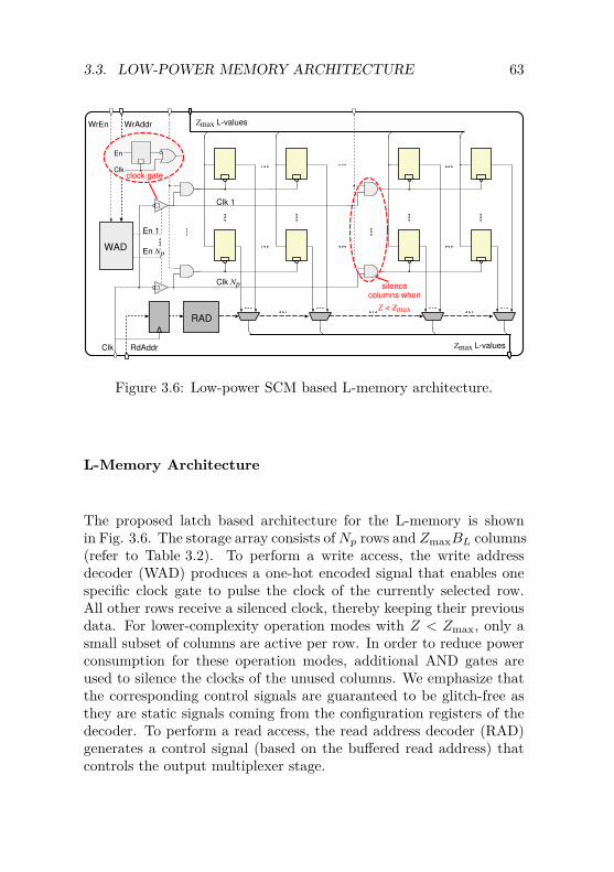
3.3. LOW-POWER MEMORY ARCHITECTURE 63
WAD
RAD
Clk
WrAddr
RdAddr
Zmax L-values
Zmax L-values
Clk 1
Clk Np silencecolumns when
Z < Zmax
WrEn
En
Clk
En 1
En Np
clock gate
Figure 3.6: Low-power SCM based L-memory architecture.
L-Memory Architecture
The proposed latch based architecture for the L-memory is shownin Fig. 3.6. The storage array consists ofNp rows and ZmaxBL columns(refer to Table 3.2). To perform a write access, the write addressdecoder (WAD) produces a one-hot encoded signal that enables onespecific clock gate to pulse the clock of the currently selected row.All other rows receive a silenced clock, thereby keeping their previousdata. For lower-complexity operation modes with Z < Zmax, only asmall subset of columns are active per row. In order to reduce powerconsumption for these operation modes, additional AND gates areused to silence the clocks of the unused columns. We emphasize thatthe corresponding control signals are guaranteed to be glitch-free asthey are static signals coming from the configuration registers of thedecoder. To perform a read access, the read address decoder (RAD)generates a control signal (based on the buffered read address) thatcontrols the output multiplexer stage.
64 CHAPTER 3. IMPLEMENTATION OF LDPC DECODING
R-Memory and Q-Buffer Architecture
In contrast to the L-memory, the individual columns in the R-memoryand Q-buffer are firmly associated with specific NCUs. For this rea-son, we partition these memories vertically into Nslice memory slices,where each slice is associated with Zmax/Nslice NCUs. This parti-tioning enables a trade-off between data locality and circuit overhead.Specifically, in one extreme case, Nslice can be chosen equal to thenumber of NCUs, effectively allocating an individual R-memory andQ-buffer slice for each NCU. This approach fully reflects the localdata processing of the message-passing algorithm, but also involves aconsiderable circuit overhead due to the numerous replicated addressdecoders and clock gates. On the other extreme, sharing a singleR-memory and Q-buffer among all NCUs minimizes circuit overheadbut further separates storage from the corresponding data processing.From a layout perspective, the good data locality implied by a largeNslice yields a more local structure, thereby facilitating placement,routing, and clock tree generation for the memories, which turns outto be associated with considerable overhead for routing and bufferinsertion for wide storage arrays.
3.4 Implementation ResultsBased on the low-power architecture described in the previous sec-tions, two ASICs optimized for the IEEE 802.11n standard6 havebeen implemented and manufactured in 90 nm CMOS technology.The first implementation uses SCMs based on a commercial standardcell library. The second ASIC is based on the first one with thecommercial SCMs replaced by custom-designed refresh-free dynamicSCMs (D-SCMs).7 The key figures of the fabricated ASICs are sum-marized in Table 3.6; the corresponding chip micrographs are shown
6The described QC-LDPC decoder architecture has also been used as basisfor the ASIC implementation presented in [65] optimized for the IEEE 802.11adstandard. By instantiating 2Zmax NCUs the implemented decoder processes twoblocks per clock cycles and achieves the multi-Gbps throughput requirements ofthe mandatory standard modes. This result proves the favorable scaling propertiesof the proposed architecture.
7The design of the D-SCMs and the integration of the second ASIC were carriedout by another PhD student. More details can be found in [24].
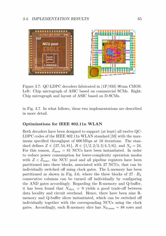
3.4. IMPLEMENTATION RESULTS 65
Ctrl
Cyclicshifter
NCU pool
L-memory
Figure 3.7: QC-LDPC decoders fabricated in (1P/8M) 90 nm CMOS.Left: Chip micrograph of ASIC based on commercial SCMs. Right:Chip micrograph and layout of ASIC based on D-SCMs.
in Fig. 3.7. In what follows, these two implementations are describedin more detail.
Optimizations for IEEE 802.11n WLAN
Both decoders have been designed to support (at least) all twelve QC-LDPC codes of the IEEE 802.11n WLAN standard [33] with the max-imum specified throughput of 600 Mbps at 10 iterations. The stan-dard defines Z ∈ {27, 54, 81}, R ∈ {1/2, 2/3, 3/4, 5/6}, and Np = 24.For this reason, Zmax = 81 NCUs have been instantiated. In orderto reduce power consumption for lower-complexity operation modeswith Z < Zmax, the NCU pool and all pipeline registers have beenpartitioned into three blocks, associated with 27 NCUs, that can beindividually switched off using clock gates. The L-memory has beenpartitioned as shown in Fig. 3.6, where the three blocks of 27 · BLconsecutive columns can be turned off individually by configuringthe AND gates accordingly. Regarding the R-memory and Q-buffer,it has been found that Nslice = 9 yields a good trade-off betweendata locality and circuit overhead. Hence, there have been nine R-memory and Q-buffer slices instantiated, which can be switched offindividually together with the corresponding NCUs using the clockgates. Accordingly, each R-memory slice has NB,max = 88 rows and
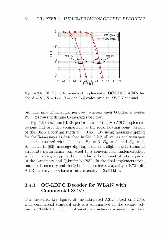
66 CHAPTER 3. IMPLEMENTATION OF LDPC DECODING
0 0.5 1 1.5 2 2.5 3 3.5 4 4.5 5 5.5
10-3
10-2
10-1
100
OMS (float.)
ASIC impl.
SNR [dB]
BLE
R
rate-1/2 rate-5/6
Figure 3.8: BLER performance of implemented QC-LDPC ASICs forthe Z = 81, R = 1/2, R = 5/6 [33] codes over an AWGN channel.
provides nine R-messages per row, whereas each Q-buffer providesNp = 24 rows with nine Q-messages per row.
Fig. 3.8 shows the BLER performance of the two ASIC implemen-tations and provides comparison to the ideal floating-point versionof the OMS algorithm (with β = 0.45). By using message-clippingfor the R-messages as described in Sec. 3.2.2, all values and messagescan be quantized with 5 bit, i.e., BL = 5, BR = 5, and BQ = 5.As shown in [62], message-clipping leads to a slight loss in terms oferror-rate performance compared to a conventional implementationwithout message-clipping, but it reduces the amount of bits requiredin the L-memory and Q-buffer by 28%. In the final implementation,both the L-memory and the Q-buffer slices have a capacity of 9.72 kbit.All R-memory slices have a total capacity of 35.64 kbit.
3.4.1 QC-LDPC Decoder for WLAN withCommercial SCMs
The measured key figures of the fabricated ASIC based on SCMswith commercial standard cells are summarized in the second col-umn of Table 3.6. The implementation achieves a maximum clock
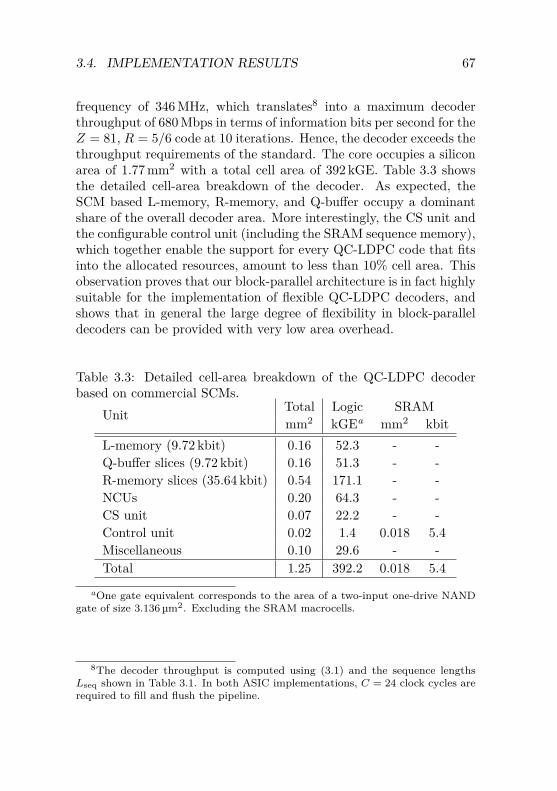
3.4. IMPLEMENTATION RESULTS 67
frequency of 346 MHz, which translates8 into a maximum decoderthroughput of 680 Mbps in terms of information bits per second for theZ = 81, R = 5/6 code at 10 iterations. Hence, the decoder exceeds thethroughput requirements of the standard. The core occupies a siliconarea of 1.77 mm2 with a total cell area of 392 kGE. Table 3.3 showsthe detailed cell-area breakdown of the decoder. As expected, theSCM based L-memory, R-memory, and Q-buffer occupy a dominantshare of the overall decoder area. More interestingly, the CS unit andthe configurable control unit (including the SRAM sequence memory),which together enable the support for every QC-LDPC code that fitsinto the allocated resources, amount to less than 10% cell area. Thisobservation proves that our block-parallel architecture is in fact highlysuitable for the implementation of flexible QC-LDPC decoders, andshows that in general the large degree of flexibility in block-paralleldecoders can be provided with very low area overhead.
Table 3.3: Detailed cell-area breakdown of the QC-LDPC decoderbased on commercial SCMs.
Unit Total Logic SRAMmm2 kGEa mm2 kbit
L-memory (9.72 kbit) 0.16 52.3 - -Q-buffer slices (9.72 kbit) 0.16 51.3 - -R-memory slices (35.64 kbit) 0.54 171.1 - -NCUs 0.20 64.3 - -CS unit 0.07 22.2 - -Control unit 0.02 1.4 0.018 5.4Miscellaneous 0.10 29.6 - -Total 1.25 392.2 0.018 5.4
aOne gate equivalent corresponds to the area of a two-input one-drive NANDgate of size 3.136 µm2. Excluding the SRAM macrocells.
8The decoder throughput is computed using (3.1) and the sequence lengthsLseq shown in Table 3.1. In both ASIC implementations, C = 24 clock cycles arerequired to fill and flush the pipeline.
68 CHAPTER 3. IMPLEMENTATION OF LDPC DECODING
Power and Energy Efficiency Measurements
Table 3.4 shows the results of our power measurements for the highest-rate codes. Besides the power consumption in terms of mW, thetable also reports energy efficiency in terms of energy per codewordbit per iteration. All measurements were performed at T = 300 Kusing typical stimuli in an AWGN scenario at a clock frequency of305 MHz. This frequency is required to meet the target throughputof 600 Mbps for the Z = 81, R = 5/6 code. It can be clearly seenthat the carefully optimized partitioning of the data path and thememories leads to substantial power reduction for lower-complexityoperation modes with Z < 81.
What is not visible from Table 3.4 is the impact of other low-power optimizations that were carried out. Regarding the L-memorybypassing described in Sec. 3.2.4, it was observed that our sequencegeneration algorithm yields a bypassing rate between 55% and 90%,depending on the structure of Hp. During bypassing, all latches inthe L-memory shown in Fig. 3.6 receive a silenced clock and thereforedo not consume any dynamic power. Furthermore, the L-values andall messages are represented using the sign-magnitude number formatsince it has been observed that this number format considerably re-duces the switching activity inside the NCUs compared to the moreconventional 2’s complement format. Finally, the deployed PPC basedearly termination scheme further improves energy efficiency for higherSNRs, where the decoding process generally requires less iterations onaverage to converge. For instance, considering an operating BLER of10−3, the early termination scheme stops decoding of the Z = 81,R = 5/6 code after an average amount of 4.2 iterations, improvingenergy efficiency by 68%.
Comparison With Prior-Art QC-LDPC Decoders
Table 3.6 provides comparison with prior-art QC-LDPC decoders [60–62, 66] and more recent implementations [67, 68] optimized for theIEEE 802.11n WLAN or IEEE 802.16e WiMAX standards. In or-der to account for differences in process technology, the results inparentheses are scaled to the 90 nm CMOS node with 1.0 V supplyvoltage. Compared to the prior-art implementations, the described
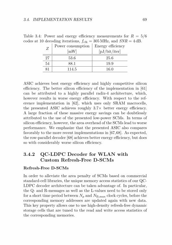
3.4. IMPLEMENTATION RESULTS 69
Table 3.4: Power and energy efficiency measurements for R = 5/6codes at 10 decoding iterations, fclk = 305 MHz, and SNR = 4 dB.
ZPower consumption Energy efficiency
[mW] [pJ/bit/iter]27 53.6 25.654 88.1 19.981 114.5 16.0
ASIC achieves best energy efficiency and highly competitive siliconefficiency. The better silicon efficiency of the implementation in [61]can be attributed to a highly parallel radix-4 architecture, which,however results in worse energy efficiency. With respect to the ref-erence implementation in [62], which uses only SRAM macrocells,the presented ASIC achieves roughly 3.7× better energy efficiency.A large fraction of these massive energy savings can be doubtlesslyattributed to the use of the presented low-power SCMs. In terms ofsilicon efficiency, however, the area overhead of the SCMs lead to worseperformance. We emphasize that the presented ASIC also comparesfavorably to the more recent implementations in [67,68]. As expected,the row-parallel decoder [68] achieves better energy efficiency, but doesso with considerably worse silicon efficiency.
3.4.2 QC-LDPC Decoder for WLAN withCustom Refresh-Free D-SCMs
Refresh-Free D-SCMs
In order to alleviate the area penalty of SCMs based on commercialstandard-cell libraries, the unique memory access statistics of our QC-LDPC decoder architecture can be taken advantage of. In particular,the Q- and R-messages as well as the L-values need to be stored onlyfor a short time period between Np and NB,max clock cycles, before thecorresponding memory addresses are updated again with new data.This key property allows one to use high-density refresh-free dynamicstorage cells that are tuned to the read and write access statistics ofthe corresponding memories.
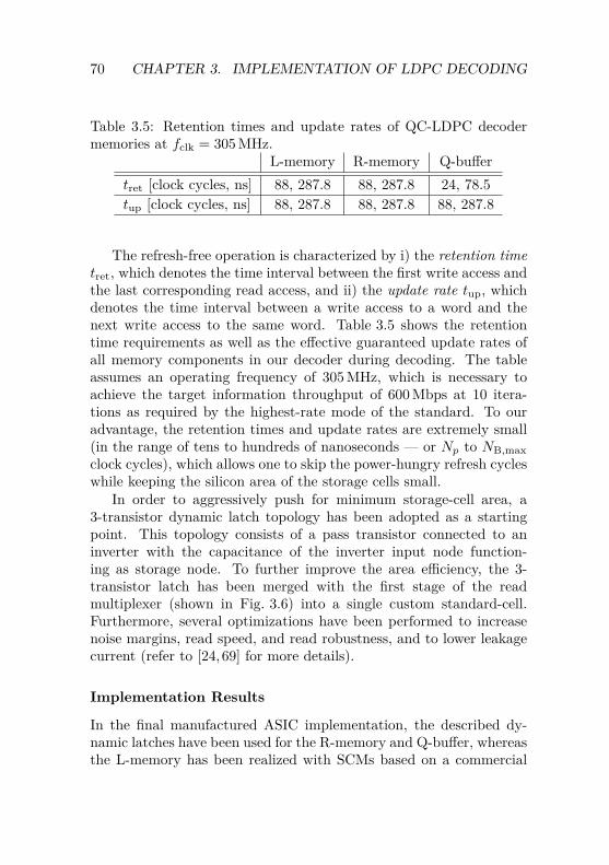
70 CHAPTER 3. IMPLEMENTATION OF LDPC DECODING
Table 3.5: Retention times and update rates of QC-LDPC decodermemories at fclk = 305 MHz.
L-memory R-memory Q-buffertret [clock cycles, ns] 88, 287.8 88, 287.8 24, 78.5tup [clock cycles, ns] 88, 287.8 88, 287.8 88, 287.8
The refresh-free operation is characterized by i) the retention timetret, which denotes the time interval between the first write access andthe last corresponding read access, and ii) the update rate tup, whichdenotes the time interval between a write access to a word and thenext write access to the same word. Table 3.5 shows the retentiontime requirements as well as the effective guaranteed update rates ofall memory components in our decoder during decoding. The tableassumes an operating frequency of 305 MHz, which is necessary toachieve the target information throughput of 600 Mbps at 10 itera-tions as required by the highest-rate mode of the standard. To ouradvantage, the retention times and update rates are extremely small(in the range of tens to hundreds of nanoseconds — or Np to NB,maxclock cycles), which allows one to skip the power-hungry refresh cycleswhile keeping the silicon area of the storage cells small.
In order to aggressively push for minimum storage-cell area, a3-transistor dynamic latch topology has been adopted as a startingpoint. This topology consists of a pass transistor connected to aninverter with the capacitance of the inverter input node function-ing as storage node. To further improve the area efficiency, the 3-transistor latch has been merged with the first stage of the readmultiplexer (shown in Fig. 3.6) into a single custom standard-cell.Furthermore, several optimizations have been performed to increasenoise margins, read speed, and read robustness, and to lower leakagecurrent (refer to [24,69] for more details).
Implementation Results
In the final manufactured ASIC implementation, the described dy-namic latches have been used for the R-memory and Q-buffer, whereasthe L-memory has been realized with SCMs based on a commercial
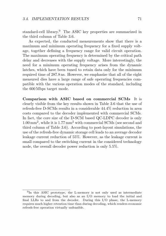
3.4. IMPLEMENTATION RESULTS 71
standard-cell library.9 The ASIC key properties are summarized inthe third column of Table 3.6.
As expected, the conducted measurements show that there is amaximum and minimum operating frequency for a fixed supply volt-age, together defining a frequency range for valid circuit operation.The maximum operating frequency is determined by the critical pathdelay and decreases with the supply voltage. More interestingly, theneed for a minimum operating frequency arises from the dynamiclatches, which have been tuned to retain data only for the minimumrequired time of 287.8 ns. However, we emphasize that all of the eightmeasured dies have a large range of safe operating frequencies com-patible with the various operation modes of the standard, includingthe 600 Mbps target mode.
Comparison with ASIC based on commercial SCMs It isclearly visible from the key results shown in Table 3.6 that the use ofrefresh-free D-SCMs results in a considerable 44.4% reduction in areacosts compared to the decoder implemented with commercial SCMs.In fact, the core size of the D-SCM based QC-LDPC decoder is only1.00 mm2, while it is 1.77 mm2 with commercial SCMs (see second andthird column of Table 3.6). According to post-layout simulations, theuse of the refresh-free dynamic storage cell leads to an average decoderleakage current reduction of 55%. However, as the leakage current issmall compared to the switching current in the considered technologynode, the overall decoder power reduction is only 5.5%.
9In this ASIC prototype, the L-memory is not only used as intermediatememory during decoding, but also as an I/O memory to load the initial andfinal LLRs to and from the decoder. During this I/O phase, the L-memoryrequires much higher retention time than during decoding, which renders economicrefresh-free operation virtually unfeasible.
72 CHAPTER 3. IMPLEMENTATION OF LDPC DECODING
Table3.6:
Com
parisonofQ
C-LD
PCdecoder
implem
entations.T
hisT
his[60]
[61][62]
[66][67]
[68]w
orkw
orka
Technology[nm
]90
90180
90180
130130
65N
om.
supplyV
DD
[V]
1.01.0
1.81.0
1.81.2
1.21.2
Mem
orytype
SCM
bD
-SCM
SRA
MSC
Mb
SRA
MSR
AM
SRA
MSC
Mb
Zm
ax81
8196
9681
6496
96Im
plement.
statussilicon
post-layoutsilicon
Core
area[m
m2]
1.771.0
3.393.5
3.392.46
3.033.36
Max.
clockfrequency
346306
83450
208125
214110
in[M
Hz]
Max.
throughput c679
60057
1667390
63728
880in
[Mbps]
Siliconeffi
ciency2.6
1.759.8
2.18.7
39.34.2
3.8in
[mm
2ns/bit]
(7.5d)
(1.1d)
(13.1d)
(1.4d)
(10.1d)
Energyeffi
ciencye
15.814.7
24320.5
38077.3
3910.9
in[pJ/bit/iter]
(37.5d)
(58.6d)
(37.2d)
(18.8d)
(10.5d)
aThe
designofthe
D-SC
Ms
andthe
ASIC
integrationw
erecarried
outby
anotherP
hDstudent.
bSCM
basedon
comm
ercialstandard-celllibrary.cA
tI
=10
iterations,R
=5/6.
dTechnologyscaling
to90
nm,V
DD
=1V
accordingto
[19]:tp
d∼
1/s,A∼
1/s 2,
Pdyn∼
1/s·(V′D
D/V
DD
) 2.eA
tnom
inalsupplyvoltage.
Chapter 4
VLSI Implementation ofTurbo Decoding
During the last decade, a vast amount of research has been conductedfocusing on the high-throughput, area-efficient, and power-efficientVLSI implementation of turbo decoders. The need of modern wirelessstandards for turbo decoders that support a large maximum blocklength and a wide range of smaller block lengths has led to a consid-erable number of economic sliding-window SISO decoder architecturesand sophisticated interleaver implementations. Interestingly, the ex-isting architectural choices for practical sliding-window SISO decodersimplementing the turbo decoder algorithms discussed in Chapter 2exhibit considerable differences in their VLSI implementation com-plexities when high code rates have to be supported. This importantaspect in the design of turbo decoders for modern and emergingwireless systems has been considered only marginally so far. In thischapter, we thoroughly investigate and compare existing and newarchitectural choices for sliding-window turbo decoders and evaluatethe associated VLSI implementation costs when the full range of coderates has to be supported.
In the first part of this chapter we provide a high-level turbo-decoder architecture overview (Sec. 4.1), where we partition the de-sign space into serial and subblock-parallel turbo decoders, followed
73
74 CHAPTER 4. IMPLEMENTATION OF TURBO DECODING
by a discussion of best-practice and new solutions for the realization ofsliding-window SISO decoders (Sec. 4.2). Furthermore, we show thatthe punctured code rate has in general a high impact on the error-rateperformance of these SISO decoder architectures. In the second partof this chapter, we consider the design of both serial (Sec. 4.3) andsubblock-parallel (Sec. 4.4) turbo decoders and show how the siliconarea, power consumption, and throughput of such decoders can beoptimized while keeping the impact of the code rate on the error-rateperformance small. Implementation results of various reference turbodecoder prototypes accompany the discussion and provide referencefor the true silicon complexity of flexible turbo decoders.
4.1 High-Level Architecture ExplorationAs shown in Fig. 1.1 the architecture’s portfolio of turbo decodersmust span more than three orders of magnitude in terms of complexitydue to the varying throughput constraints of modern and emergingwireless standards. In order to cover this large gap, designers ofturbo decoders mainly rely on two architecture types: i) serial and ii)subblock-parallel turbo decoder architectures.1 These two high-levelarchitecture types are illustrated in Fig. 4.1 and briefly described inwhat follows.
4.1.1 Serial ArchitectureSerial turbo decoder designs, e.g., [25, 72–75], were among the firstimplementations of turbo decoders. As shown in the upper partof Fig. 4.1, serial turbo decoders deploy P = 1 SISO decoder whichis time-shared among the two half-iterations. The input memorystores the depunctured LLR values Ls, Lp1, and Lp2 of one codeblock and provides the SISO decoder with the proper LLRs duringdecoding. The intermediate memory is used to exchange the extrinsic
1The shuffled turbo decoder [70] has evolved as another interesting architecturetype which processes the two subsequent half-iterations concurrently with multipleSISO decoders. While shuffled turbo decoding provides an additional degreeof parallelism compared to the subblock-parallel architecture, it may lead to aconsiderable error-rate performance degradation [71]. Shuffled turbo decoding isnot considered in this thesis.
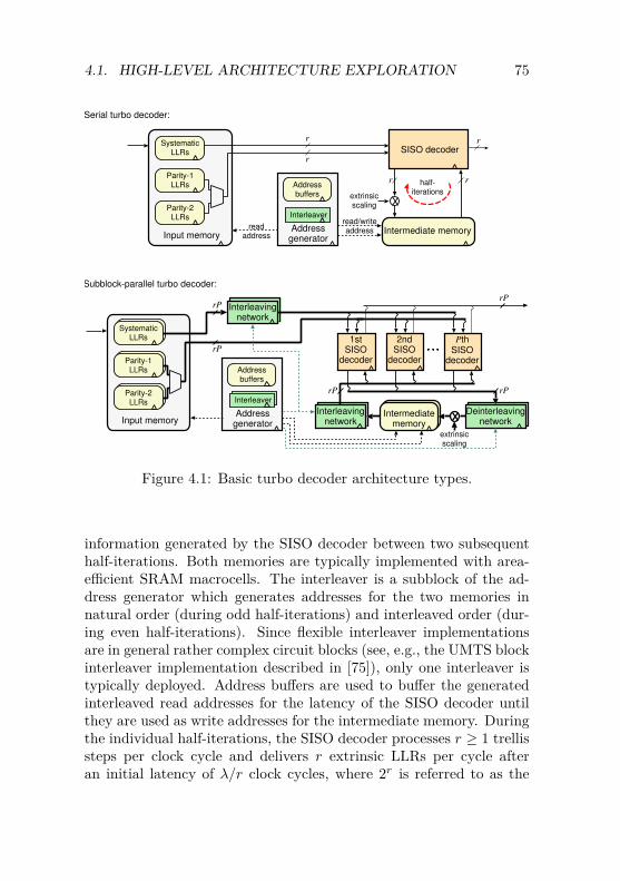
4.1. HIGH-LEVEL ARCHITECTURE EXPLORATION 75
Serial turbo decoder:
SISO decoder
Intermediate memoryAddressgenerator
half-iterations
readaddress
read/writeaddress
Interleaver
Input memory
SystematicLLRs
Parity-1LLRs
Parity-2LLRs
Addressbuffers
Intermediatememory
1stSISO
decoder
2ndSISO
decoder
PthSISO
decoder
Intermediatememory
Subblock-parallel turbo decoder:
Input memory
SystematicLLRs
Parity-1LLRs
Parity-2LLRs
Addressgenerator
Interleaver
Addressbuffers
Interleavingnetwork
Interleavingnetwork
Deinterleavingnetwork
r
rP
r
r
rr
rP
rP
rPrP
extrinsicscaling
extrinsicscaling
Figure 4.1: Basic turbo decoder architecture types.
information generated by the SISO decoder between two subsequenthalf-iterations. Both memories are typically implemented with area-efficient SRAM macrocells. The interleaver is a subblock of the ad-dress generator which generates addresses for the two memories innatural order (during odd half-iterations) and interleaved order (dur-ing even half-iterations). Since flexible interleaver implementationsare in general rather complex circuit blocks (see, e.g., the UMTS blockinterleaver implementation described in [75]), only one interleaver istypically deployed. Address buffers are used to buffer the generatedinterleaved read addresses for the latency of the SISO decoder untilthey are used as write addresses for the intermediate memory. Duringthe individual half-iterations, the SISO decoder processes r ≥ 1 trellissteps per clock cycle and delivers r extrinsic LLRs per cycle afteran initial latency of λ/r clock cycles, where 2r is referred to as the
76 CHAPTER 4. IMPLEMENTATION OF TURBO DECODING
radix of the trellis processing inside the SISO decoder and λ de-notes the architecture-specific SISO-decoder latency in terms of trellissteps. While higher-radix trellis processing improves the throughputof turbo decoders, the required memory bandwidths linearly increasewith r. Unfortunately, increasing the memory bandwidths by storingmore words per address or by partitioning the memories into smallermemory blocks is in general not possible without memory access con-flicts that arise from the pseudo-randomly interleaved memory accessscheme during even half-iterations. Such access conflicts must beavoided by interleaver-specific precaution mechanisms, leading to aninterleaving bottleneck which typically comes at the cost of a through-put penalty and increased implementation complexity [19].
4.1.2 Subblock-Parallel ArchitectureSubblock-parallel turbo decoders, e.g., [26, 76–83], achieve consid-erably higher throughput than serial turbo decoders by deployingmultiple P > 1 SISO decoders as shown in the lower part of Fig. 4.1.In particular, the trellis processed in each half-iteration is dividedinto P subblocks of length KP = K/P and decoded by the P SISOdecoders concurrently. Clearly, the large memory bandwidth requiredin subblock-parallel turbo decoding exacerbates the interleaver bottle-neck in general. However, in this thesis we consider subblock-parallelturbo decoding only in conjunction with contention-free interleavers,such as quadratic permutation-polynomial (QPP) interleavers [40,84]as specified for LTE and LTE-A [39]. QPP interleavers have a well-defined algebraic structure and can thus be implemented with verylow complexity [80]. In addition, the contention-free property ofsuch interleavers allows the P SISO decoders to access the memorieswithout any conflicts. This can be achieved, for instance, by using afolded memory architecture for the input and intermediate memoriesas proposed in [80] where each memory address corresponds to PLLRs that are arranged in ascending order with constant trellis indexoffset KP . During the odd half-iterations, the P LLRs are naturallyassociated with the P SISO decoders. During even half-iterations, theP LLRs are also associated with the P decoders, however, in inter-leaved order. Thus, the systematic input LLRs of the SISO decodersmust first be passed through an interleaving network (see Fig. 4.1)
4.1. HIGH-LEVEL ARCHITECTURE EXPLORATION 77
which permutes the P LLRs according to the properties of the par-ticular interleaver and the time step in the decoding process. Theextrinsic LLRs generated by the SISO decoders are permuted backinto natural order by the deinterleaving network. In order to enhancethe throughput for a specific P , practical subblock-parallel turbodecoders typically rely on radix-4, i.e., r = 2, trellis processing. Inconjunction with QPP interleavers, the increased memory bandwidthin this case can be easily supported by partitioning all memories andinterleaving networks shown in Fig. 4.1 into two parts, where one partis associated with the even LLR indices and the other part with theodd indices [80,81].
4.1.3 Throughput of Turbo DecodersThe decoding throughput of a turbo decoder is defined as decodedinformation bits per second. It is assumed that all SISO decoders andall other components operate at a clock frequency fclk. In this case,the throughput of a P = 1 serial or P > 1 subblock-parallel turbodecoder becomes
θP (Ih, λ) = K
Ih( KrP + λr + C)
fclk
= K
K + P (λ+ rC)rPfclk
Ih, (4.1)
where C represents an additional latency in every half-iteration, com-ing from pipelining. In order to have a technology-independent mea-sure for the throughput, i.e., one that is independent of the clockfrequency, the normalized throughput in terms of decoded informationbits per clock cycle θP,N = θP /fclk is also considered.
The Parallel Turbo-Decoder Predicament
Fig. 4.2 depicts the normalized throughput θP,N for different P , dif-ferent values of SISO-decoder latency λ, and fixed number of half-iterations Ih. The idealistic throughput assuming an ideal decoderwith λ = 0 and C = 0 is also shown. It can be clearly observed thatthe SISO-decoder latency λ prevents the turbo decoder throughputfrom scaling linearly in P . In particular, the throughput gain achieved
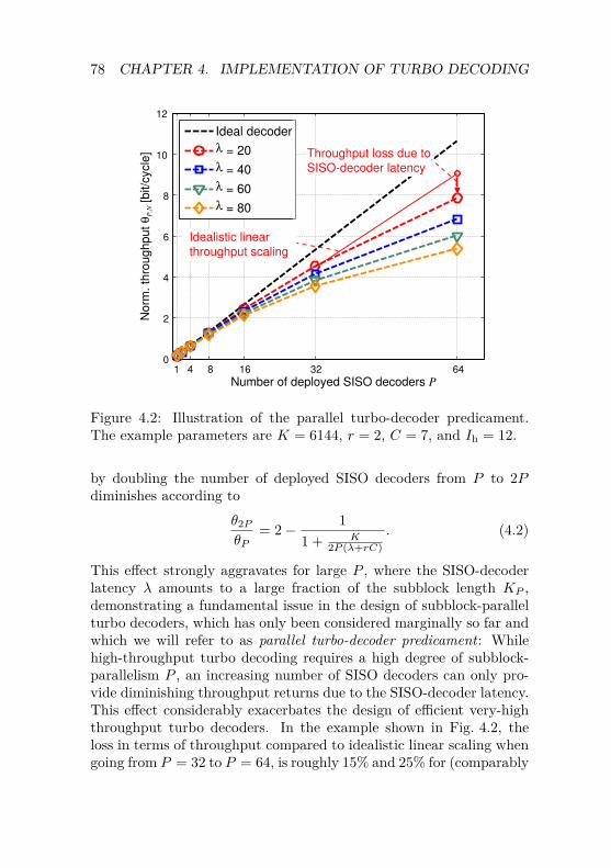
78 CHAPTER 4. IMPLEMENTATION OF TURBO DECODING
1 4 8 16 32 640
2
4
6
8
10
12
Number of deployed SISO decoders P
Norm
. th
roughput
θP,N [bit/c
ycle
]Ideal decoder
λ = 20
λ = 40
λ = 60
λ = 80
Idealistic linear
throughput scaling
Throughput loss due to
SISO-decoder latency
Figure 4.2: Illustration of the parallel turbo-decoder predicament.The example parameters are K = 6144, r = 2, C = 7, and Ih = 12.
by doubling the number of deployed SISO decoders from P to 2Pdiminishes according to
θ2P
θP= 2− 1
1 + K2P (λ+rC)
. (4.2)
This effect strongly aggravates for large P , where the SISO-decoderlatency λ amounts to a large fraction of the subblock length KP ,demonstrating a fundamental issue in the design of subblock-parallelturbo decoders, which has only been considered marginally so far andwhich we will refer to as parallel turbo-decoder predicament: Whilehigh-throughput turbo decoding requires a high degree of subblock-parallelism P , an increasing number of SISO decoders can only pro-vide diminishing throughput returns due to the SISO-decoder latency.This effect considerably exacerbates the design of efficient very-highthroughput turbo decoders. In the example shown in Fig. 4.2, theloss in terms of throughput compared to idealistic linear scaling whengoing from P = 32 to P = 64, is roughly 15% and 25% for (comparably
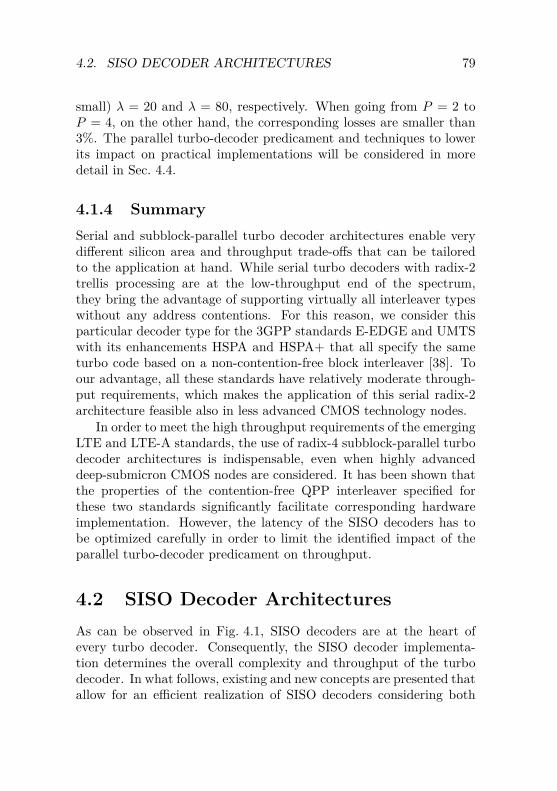
4.2. SISO DECODER ARCHITECTURES 79
small) λ = 20 and λ = 80, respectively. When going from P = 2 toP = 4, on the other hand, the corresponding losses are smaller than3%. The parallel turbo-decoder predicament and techniques to lowerits impact on practical implementations will be considered in moredetail in Sec. 4.4.
4.1.4 SummarySerial and subblock-parallel turbo decoder architectures enable verydifferent silicon area and throughput trade-offs that can be tailoredto the application at hand. While serial turbo decoders with radix-2trellis processing are at the low-throughput end of the spectrum,they bring the advantage of supporting virtually all interleaver typeswithout any address contentions. For this reason, we consider thisparticular decoder type for the 3GPP standards E-EDGE and UMTSwith its enhancements HSPA and HSPA+ that all specify the sameturbo code based on a non-contention-free block interleaver [38]. Toour advantage, all these standards have relatively moderate through-put requirements, which makes the application of this serial radix-2architecture feasible also in less advanced CMOS technology nodes.
In order to meet the high throughput requirements of the emergingLTE and LTE-A standards, the use of radix-4 subblock-parallel turbodecoder architectures is indispensable, even when highly advanceddeep-submicron CMOS nodes are considered. It has been shown thatthe properties of the contention-free QPP interleaver specified forthese two standards significantly facilitate corresponding hardwareimplementation. However, the latency of the SISO decoders has tobe optimized carefully in order to limit the identified impact of theparallel turbo-decoder predicament on throughput.
4.2 SISO Decoder ArchitecturesAs can be observed in Fig. 4.1, SISO decoders are at the heart ofevery turbo decoder. Consequently, the SISO decoder implementa-tion determines the overall complexity and throughput of the turbodecoder. In what follows, existing and new concepts are presented thatallow for an efficient realization of SISO decoders considering both
80 CHAPTER 4. IMPLEMENTATION OF TURBO DECODING
the max-log-BCJR and the soft-output Viterbi algorithms discussedin Chapter 2.
Sliding-Window Trellis Processing
Recall from Chapter 2 that both the max-log-BCJR algorithm andSOVA are based on recursive computations through the trellis ofthe component convolutional code. The straightforward implemen-tation of these algorithms thus leads to memory requirements thatare proportional to |S| ·K , i.e., the number of trellis states timesthe trellis length. Considering the large block lengths of recent andemerging wireless standards, these memory requirements have becomeprohibitively large for economic ASIC implementations. The key toavoid these high memory requirements is to employ sliding-windowtrellis processing inside the SISO decoders considered — a well-knownapproach that originally emerged from practical Viterbi decoder im-plementations. With this technique, the trellis is processed on aper-window basis, and only the metrics within the processed windowsneed to be stored.
4.2.1 Sliding-Window BCJR Architecture
The sliding-window BCJR decoder divides the trellis (or trellis sub-block for P > 1) into windows comprising W ≤ KP trellis steps, whereW denotes the window length. The NW = dKP /W e windows areprocessed sequentially in ascending order. In particular, the forwardstate metrics Ak(s) of a specific window are computed and storedaccording to (2.36) before the corresponding intrinsic/extrinsic LLRsare obtained simultaneously with the backward state metrics Bk(s)as in (2.37) and (2.38).
The recursive computation of forward state metrics requires thatthe forward state metrics computed at the end of a specific windown (n = 1, . . . NW ) are used as initial forward state metrics for theadjacent window n+1. For the backward recursion, however, suitableinitial backward state metrics are missing since the recursion evolvesin backward direction. To avoid serious performance degradation,initial backward state metrics must be estimated for each window. In
4.2. SISO DECODER ARCHITECTURES 81
A
A
A
B
LLR
B
LLR
B
LLR
Dummy
Dummy
Dummy
Dummy
W
λACQ/r
time
bit
2W
3W
W/r 2W/r0
3W/r 4W/r
4W
A
(a) ACQ based architecture.
A
A
A
B
LLR
B
LLR
B
LLR
λSMP/r
time
bit
W/r 2W/r0
3W/r 4W/r
4W
AB
LLR
W
2W
3W
State metric propagation
to next iterationS
tate
metr
ic p
ropagation
from
pre
vio
us ite
ration
(b) SMP based architecture.
Figure 4.3: Processing schedule of the ACQ/SMP based sliding-window BCJR decoder architectures illustrated using the conventionalgraphical representation from [87].
order to solve this window-boundary initialization issue, two main ap-proaches have evolved in the open literature, resulting in two generalsliding-window BCJR architecture types. The conventional architec-ture, which has been widely adopted and is the basis of many recentpractical turbo decoder implementations (e.g., [72–75, 77–80]), relieson acquisition runs (ACQ) [85] to initialize the backward state met-rics. More recently, initialization by state metric propagation (SMP)across iterations [86] has gained an increasing attention. It is im-portant to note that these techniques must also be used across thesubblock boundaries in subblock-parallel turbo decoders to estimatereliable forward and backward state metrics at the subblock edges.
Architecture based on ACQ
Conventionally, a dummy backward recursion, i.e., acquisition run ofacquisition length AL trellis steps, over window n+ 1 is performed togenerate a set of reliable initial backward state metrics for windown. Each acquisition run is initialized with all-zero metrics. Theprocessing schedule of this sliding-window BCJR decoder is depicted
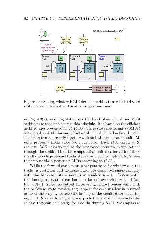
82 CHAPTER 4. IMPLEMENTATION OF TURBO DECODING
G
Intrinsic/extrinsic
LLR computation
Radix-2r
ACS
unit
init
Alpha
memory
Forward
SMU
BCJR decoder based on ACQ
’0’
G G
Gamma
memory
Gamma
memory
Backward
SMU
Dummy
SMU
radix-2r
branch-metric
generation
Radix-2r
ACS
unit
Radix-2r
ACS
unit
|S|× |S|× |S|×
LA
Lp
Ls
LE
LD
b
Figure 4.4: Sliding-window BCJR decoder architecture with backwardstate metric initialization based on acquisition runs.
in Fig. 4.3(a), and Fig. 4.4 shows the block diagram of our VLSIarchitecture that implements this schedule. It is based on the efficientarchitectures presented in [25,75,80]. Three state metric units (SMUs)associated with the forward, backward, and dummy backward recur-sion operate concurrently together with an LLR computation unit. Allunits process r trellis steps per clock cycle. Each SMU employs |S|radix-2r ACS units to realize the associated recursive computationsthrough the trellis. The LLR computation unit uses for each of the rsimultaneously processed trellis steps two pipelined radix-2 ACS treesto compute the a-posteriori LLRs according to (2.38).
While the forward state metrics are generated for window n in thetrellis, a-posteriori and extrinsic LLRs are computed simultaneouslywith the backward state metrics in window n − 1. Concurrently,the dummy backward recursion is performed over window n + 1 (seeFig. 4.3(a)). Since the output LLRs are generated concurrently withthe backward state metrics, they appear for each window in reversedorder at the output. To keep the latency of the architecture small, theinput LLRs in each window are expected to arrive in reversed orderso that they can be directly fed into the dummy SMU. We emphasize
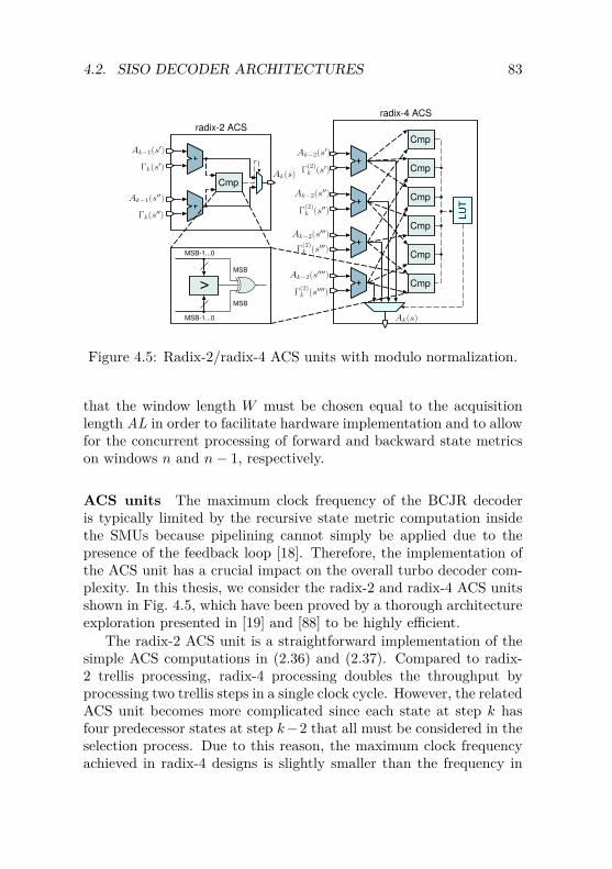
4.2. SISO DECODER ARCHITECTURES 83
Cmp
>MSB
MSB
MSB-1...0
MSB-1...0
Cmp
Cmp
Cmp
Cmp
Cmp
Cmp
LU
T
radix-2 ACS
radix-4 ACS
Ak−1(s′)
Γk(s′)
Ak−1(s′′)
Γk(s′′)
Ak(s)
Ak−2(s′)
Γ(2)k (s′)
Ak−2(s′′)
Γ(2)k (s′′)
Ak−2(s′′′)
Γ(2)k (s′′′)
Ak−2(s′′′′)
Γ(2)k (s′′′′)
Ak(s)
Figure 4.5: Radix-2/radix-4 ACS units with modulo normalization.
that the window length W must be chosen equal to the acquisitionlength AL in order to facilitate hardware implementation and to allowfor the concurrent processing of forward and backward state metricson windows n and n− 1, respectively.
ACS units The maximum clock frequency of the BCJR decoderis typically limited by the recursive state metric computation insidethe SMUs because pipelining cannot simply be applied due to thepresence of the feedback loop [18]. Therefore, the implementation ofthe ACS unit has a crucial impact on the overall turbo decoder com-plexity. In this thesis, we consider the radix-2 and radix-4 ACS unitsshown in Fig. 4.5, which have been proved by a thorough architectureexploration presented in [19] and [88] to be highly efficient.
The radix-2 ACS unit is a straightforward implementation of thesimple ACS computations in (2.36) and (2.37). Compared to radix-2 trellis processing, radix-4 processing doubles the throughput byprocessing two trellis steps in a single clock cycle. However, the relatedACS unit becomes more complicated since each state at step k hasfour predecessor states at step k−2 that all must be considered in theselection process. Due to this reason, the maximum clock frequencyachieved in radix-4 designs is slightly smaller than the frequency in
84 CHAPTER 4. IMPLEMENTATION OF TURBO DECODING
radix-2 implementations [88]. Radix-4 designs are consequently lessefficient in terms of area divided by throughput (i.e., silicon efficiency).When striving for highest throughput, the smaller silicon efficiency istypically accepted. Note that radix-4 SMUs generate only the statemetrics related to even trellis steps. For the computation of thea-posteriori LLRs, the state metrics related to odd trellis steps arecomputed on-the-fly in the LLR computation unit.
In order to limit the dynamic range of the computed state metrics,modulo normalization [89] is applied inside the ACS units. Thisnormalization method bases on the fact that the difference betweenany two state metrics at any trellis step k is upper-bounded if thebranch metrics are upper-bounded as well. Thus, this approach tracksthe difference between the state metrics rather than their absolutevalues, which can be simply achieved by exploiting the wrappingproperty of two’s complement numbers in conjunction with a largeenough state metric wordwidth BSM. For the considered |S| = 8code, modulo normalization enables one to limit BSM to 10 bit.
Metric memories In order to align the sequence of operation intime, two Gamma memories are required that buffer branch metricsover two windows n− 1 and n, respectively. Each of these memoriesis alternately filled with new metrics in every second window, and theforward and backward SMUs access the two memories in alternatingorder. Each Gamma memory requires at least W/r addresses andstores at each address the sum Ls + LA concatenated with Lp for rconsecutive trellis steps. Note that only these two values are requiredper trellis step to compute the branch metrics according to (2.39). Theactual branch metrics for all possible state transitions are generatedat the output of the memory in a small logic block G.
Since the forward state metrics are obtained one window beforethe corresponding backward state metrics, they must be buffered inthe Alpha memory for the duration of one window. The bufferedmetrics are retrieved from this memory in backward direction andpassed together with the computed backward state metrics into theLLR computation unit. The Alpha memory must thus provide at leastW/r addresses, and conventionally stores |S| forward state metricsper address. Both the Gamma memory and Alpha memory must be
4.2. SISO DECODER ARCHITECTURES 85
realized as two-port memories in order to support concurrent read andwrite access per clock cycle.
SISO-decoder latency As illustrated in Fig. 4.3(a), the first ex-trinsic LLRs are generated after a latency of two windows, as a conse-quence of the fact that the two Gamma memories must be completelyfilled before the backward SMU can start its operation. Therefore,the SISO-decoder latency of this architecture type is λACQ = 2W .The architecture suffers from an additional latency C between 3 and7 clock cycles coming from pipelining, which is typically employed tolimit the critical path to the ACS delay.
Architecture based on SMP
The SMP based architecture omits explicit acquisition runs. Instead,the backward state metrics in window n are initialized with the back-ward state metrics computed in the last step at the end of windown + 1 during the previous turbo iteration. As a consequence of thisapproach, the first two half-iterations of the turbo decoder are per-formed with uninitialized backward state metrics. For this reason,the SMP based turbo decoder exhibits a slightly slower convergencespeed than the turbo decoder based on ACQ [25,71,90].
The processing schedule and VLSI architecture block diagram ofthis approach are shown in Fig. 4.3(b) and Fig. 4.6, respectively. Theinput LLRs in each window now arrive in natural order and aredirectly fed into the forward SMU. In contrast to the ACQ basedarchitecture, no dummy SMU, and therefore only one Gamma memoryare required. However, an SMP memory is necessary to buffer the|S| initial backward state metrics at all window boundaries for bothhalf-iterations. Accordingly, the SMP memory must provide 2 · NWaddresses. As opposed to the Gamma and Alpha memories, the SMPmemory can be realized as a less complex single-port memory, sinceonly one read and write access must be performed per window.
SISO-decoder latency Observe from Fig. 4.3(b) that the first ex-trinsic LLRs are now delivered already after a latency of one window,since the backward SMU is not required to wait for the completionof an acquisition run. Hence, the SISO-decoder latency of the SMP
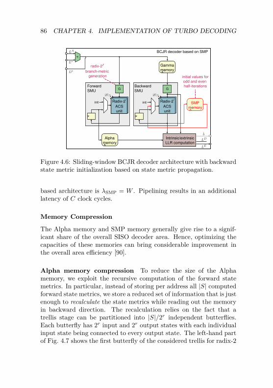
86 CHAPTER 4. IMPLEMENTATION OF TURBO DECODING
G
Intrinsic/extrinsic
LLR computation
Radix-2r
ACS
unit
init
Alpha
memory
Forward
SMU
BCJR decoder based on SMP
G
Gamma
memory
Backward
SMU
Radix-2r
ACS
unit
SMP
memory
radix-2r
branch-metric
generation initial values for
odd and even
half-iterations
init
LE
LD
b
|S|× |S|×
LA
Ls
Lp
Figure 4.6: Sliding-window BCJR decoder architecture with backwardstate metric initialization based on state metric propagation.
based architecture is λSMP = W . Pipelining results in an additionallatency of C clock cycles.
Memory Compression
The Alpha memory and SMP memory generally give rise to a signif-icant share of the overall SISO decoder area. Hence, optimizing thecapacities of these memories can bring considerable improvement inthe overall area efficiency [90].
Alpha memory compression To reduce the size of the Alphamemory, we exploit the recursive computation of the forward statemetrics. In particular, instead of storing per address all |S| computedforward state metrics, we store a reduced set of information that is justenough to recalculate the state metrics while reading out the memoryin backward direction. The recalculation relies on the fact that atrellis stage can be partitioned into |S|/2r independent butterflies.Each butterfly has 2r input and 2r output states with each individualinput state being connected to every output state. The left-hand partof Fig. 4.7 shows the first butterfly of the considered trellis for radix-2
4.2. SISO DECODER ARCHITECTURES 87
Ak−1(s0)
Ak−1(s1)
Ak(s0)Γk(s0, s0)
Γk(s0, s4) Ak(s4)
s0
s4
s0
s1
Radix-2 butterfly
Dec. logic
Ak(s4)
Ak(s0)
d(s0)
d(s4)
Ak−1(s1)
Γk(s0, s0)
Γk(s0, s4)
Γk(s1, s0)
Γk(s1, s4)
Ak−1(s1)
Ak−1(s0)
Radix-2 state metric recalculation
Selected paths
Hidden state metric
(must be stored in Alpha memory)
d(s0)
d(s4)
d(s) Decision bit of state s
Figure 4.7: Illustration of Alpha memory compression. Left: Radix-2butterfly. Right: Radix-2 recalculation of forward state metrics. Thisrecalculation must be performed for all butterflies concurrently. Thevalues provided by the Alpha memory are highlighted in red.
(i.e., r = 1) trellis processing. Assuming that the 2r output statemetrics of the butterfly are known, the input state metrics can berecomputed using the ACS decisions generated in the forward SMUand the branch metrics that correspond to these decisions. The rdecision bits for every trellis state are stored in the Alpha memory. Incases where all 2r output states are based on the same input statemetric, however, the remaining 2r − 1 input state metrics cannotbe recomputed and, thus, must be stored along with the decisionbits in the Alpha memory. Hence, the wordwidth of the compressedAlpha memory is |S| · ((1− 1/2r)BSM + r) bit. The forward statemetrics required at the end of each window to start the recursiverecalculation can be taken directly from the output of the forwardSMU. The branch metrics are provided by the backward SMU, whichuses them concurrently to perform the backward recursion.
The described approach is especially efficient for radix-2 trellisprocessing. Assuming |S| = 8 and a typical state metric wordwidthof BSM = 10, only 4 forward state metrics and 8 decision bits arestored per address. This reduces the capacity of the Alpha memoryby 40% with respect to the standard approach where all |S| state
88 CHAPTER 4. IMPLEMENTATION OF TURBO DECODING
metrics are stored, while only a small overhead of two subtractors perbutterfly is required to perform the recalculations (see right-hand partof Fig. 4.7). For radix-4, in contrast, the savings in terms of capacityare considerably lower since now 6 state metrics and 16 decision bitsmust be stored in each row.
SMP memory compression To reduce the size of the SMP mem-ory, we exploit the fact that only the relative distance between statemetrics is relevant when employing modulo normalization. Thus, wenormalize the initial state metrics by subtracting the first state metricfrom all |S| − 1 remaining ones. Only these |S| − 1 normalized statemetrics must be stored for every window boundary in the compressedSMP memory, which already reduces the capacity by 12% (at |S| = 8)with respect to the standard approach where all |S| initial metrics arestored. Furthermore, the normalization reduces the dynamic range ofthe metrics, which allows one in addition to saturate the normalizedstate metrics to smaller wordwidth BSMP < BSM bit. Simulationsshow that the initial metrics can be saturated at least from 10 to 8 bitwithout any noticeable impact on performance [90]. This correspondsto a total capacity reduction of 30%. To our advantage, the SMPmemory is only accessed once per window. Hence, there are enoughclock cycles available to realize the normalization of the initial statemetrics with very low complexity using a single subtractor.
4.2.2 Improved-SOVA ArchitectureSOVA decoder architectures preferably employ the two-step proceduredescribed in Sec. 2.3.4, i.e., they first determine the ML path and thentrack for each trellis state along the ML path the discarded concurrentpath for U trellis steps, thereby updating the U related LLR magni-tudes as formulated in (2.43) and (2.44) and illustrated in Fig. 2.9.The main implementation challenge arises from the constraint thatthe update of the U LLR magnitudes must be performed in a singleclock cycle. If this constraint was not achieved, the decoder wouldsuffer from a considerable throughput degradation compared to theBCJR architectures previously described.
The upper-left part of Fig. 4.8 shows the high-level block diagramof the proposed SOVA decoder architecture. It is based on the de-facto
4.2. SISO DECODER ARCHITECTURES 89
∆k
BM
U1
AC
S1
unit
RE
U1
BM
U2
RE
U2
AL-s
tep
shift re
gis
ter
Update
unit
s k
Γk(s
′ ,s)
Γk(s
′ ,s)
dk(s)
dk(s)
dk
i k−l
∆k
∆c k−l
∆k(s)
LA k
Lp k
Ls k
AL s
teps
U s
teps
8 p
ara
llel
AC
S1 u
nits
8 p
ara
llel
AC
S2 u
nits
LE k
U s
teps
U1 s
teps
s k
3
dk(s
0)
1
dk(s
7)
1
∆k(s
0)
5
∆k(s
7)
53
∆c k−1
∆c k−2
dk
i k−1
i k−2
LD k
AC
S2
unit
Ak(s)
dk(s)
∆k(s)
AL s
teps
1
dk(s
0)
1
dk(s
7)
33
0 7
U-stepshift register
|·|
MS
B
MS
BM
SB
10 7
10
5
10 7
10
Γk(s
′ 0,s)
Γk(s
′ 1,s)
Ak−1(s
′ 0)
Ak−1(s
′ 1)
Ak(s)
Ak(s)
Update
rule
s1 a
nd 2
Update
rule
1∆
k
i k−1
∆c k−1
i k−U1
|LD k|
RE
U1
AC
S2 u
nit
Update
unit
RE
U2
Max tracker
b k
|LD k−1|
|LD k−(U
1−1)|
|LD k−U1|
|LD k−U|
Figu
re4.
8:Sl
idin
g-w
indo
wSI
SOde
code
rar
chite
ctur
eba
sed
onth
eim
prov
edSO
VA.
90 CHAPTER 4. IMPLEMENTATION OF TURBO DECODING
standard architecture described in [91], but additionally supports thesecond update rule in (2.44). Recall from Sec. 2.3.4 that this secondupdate rule is key to make SOVA based turbo decoders competitivein terms of error-rate performance to turbo decoders based on themax-log-BCJR algorithm. The architecture essentially consists of twoparts. The first part is identical to a hard-output Viterbi decoder anddelivers the ML path. The second part is concerned with updatingthe LLR magnitudes based on the determined ML path. To simplifythe ensuing discussion, the architecture in Fig. 4.8 is depicted forradix-2 trellis processing with |S| = 8. The extension to radix-4 isstraightforward.
Computation of ML Path
The soft-inputs are first pre-processed and then used to calculate thebranch metrics inside the branch metric unit (BMU1)2. A set of|S| = 8 parallel ACS units recursively compute the state metrics Ak(s)in forward direction and generate the decision bits dk(s). These ACSunits are identical to the one shown in Fig. 4.5. To calculate theML path with small latency in a sliding-window fashion, we considerthe flip-flop based register-exchange (RE) technique [92], which isan alternative to the more common memory based trace-back tech-nique [92, 93]. The main motivation for this choice is that the REtechnique generally qualifies for higher clock frequencies than thememory based trace-back technique. Furthermore, for convolutionalcodes with a small number of states (and for small AL), the areaadvantage of the memory based technique becomes insignificant [91].
The first RE unit (REU1) discloses in every clock cycle the nextstate sk along the ML path after an initial latency of AL trellis steps,where AL corresponds to the acquisition length of the trace-backperformed by REU1. As shown in Fig. 4.8, REU1 has a very simplestructure comprising a two-dimensional array of registers and multi-plexers, where the columns represent the states in the current trelliswindow and the AL successive columns are interconnected throughthe multiplexers according to the trellis structure. All multiplexers
2The BMU is virtually identical to the branch metric generation unit G in thepresented BCJR decoder architectures. However, in the context of Viterbi andsoft-output Viterbi decoders, BMU is the common terminology.
4.2. SISO DECODER ARCHITECTURES 91
are directly controlled by the incoming decision bits. The i-th row ofthe array represents the AL last states of the survivor path at the i-thstate at trellis step k+ AL. If AL is chosen large enough, all survivorpaths at step k+AL emanate from the ML state at step k. Thus, thisML state sk is normally present at the output of all registers in thelast column. To resolve conflicts in rare cases where different statesappear at the outputs of REU1, we choose the one that correspondsto the maximum current state metric tracked by a max-tracker unit.
Update of LLR Values
The right-hand part of the block diagram amounts to tracing theconcurrent paths, updating the LLR magnitudes, and computing theextrinsic LLRs relying on the disclosed ML path. Rather than buffer-ing the outputs of the ACS1 units for the latency of REU1 as donein [91], we instantiate BMU2 and a second set of ACS units to recom-pute the decision bits and generate the magnitudes ∆k(s). As shownin Fig. 4.8, the ACS2 architecture used to realize this functionalityis only slightly more complex than the ACS1 architecture. Using thedecisions and magnitudes, a second RE unit (REU2) discloses in everyclock cycle after an initial latency of AL + U trellis steps all metricsof the next concurrent path along the trellis. To this end, REU2employs two RE subblocks that work according to the same principleas REU1 (see Fig. 4.8). The first subblock generates U indicator bitsik−l which indicate for the concurrent path at trellis step k whetherthe related decision bits are identical or different to the ones alongthe ML path, i.e., ik−l = 1 when dk−l 6= dck−l and ik−l = 0 otherwise.The second subblock provides the U1 − 1 magnitudes ∆c
k−l that arerequired to implement the second update rule.
The update unit updates all U LLR magnitudes |LDk−l| in a singleclock cycle using the metrics provided by REU2 and relying on asimple shift-register structure as illustrated in the lower-right partof Fig. 4.8. In the first U1 stages, the LLR magnitudes are updatedusing both update rules in (2.43) and (2.44), while the values inthe remaining U − U1 stages are updated according to the first ruleonly. After an initial latency of AL + U trellis steps, the updateunit eventually delivers the extrinsic LLRs. Hence, the SISO-decoderlatency of the proposed architecture is λSOVA = AL + U .
92 CHAPTER 4. IMPLEMENTATION OF TURBO DECODING
We emphasize that the support of the second update rule in (2.44)only affects the implementation complexity of REU2 and the updateunit. The corresponding increase in complexity compared to a con-ventional SOVA decoder that implements the original rule only is fullydetermined by U1. Thus, the parameter U1 enables an interesting per-formance/complexity trade-off. Our simulations and the evaluationsin [44] have shown that U1 can typically be chosen considerably smallerthan the update window length U without degrading performance.Similarly, the update window length U is typically smaller than theacquisition length AL.
Stand-Alone SOVA Decoder ASIC Implementation Results
In order to prove the efficiency of the proposed architecture, a stand-alone ASIC prototype has been taped-out and manufactured in 180 nmCMOS. The ASIC contains two SOVA decoder cores, where one hasbeen fully pipelined and optimized for maximum operating clock fre-quency, while the other has not been pushed to its performance limit(in terms of critical path delay). Table 4.1 summarizes the measuredkey characteristics of both decoder cores and provides comparison tothe prior-art SOVA decoder implementation in [91]. To achieve a goodtrade-off between complexity and error-rate performance (assumingunpunctured operation), the parameters AL = 30, U = 21, andU1 = 6 have been carefully optimized and the input LLRs quantizedto 5 bit. The state metrics have been quantized to 10 bit and themagnitudes to 5 bit.
Compared to the prior-art SOVA decoder, our high-speed coreshows improved silicon efficiency and considerably lower power con-sumption. We mainly attribute this advantage to our choice of trad-ing flip-flops for combinational logic by instantiating a BMU2 anda second set of ACS units. Post-layout power simulations on themanufactured layout show that this optimization enables power sav-ings of roughly 15%, while the savings in silicon area amount to 5%.We furthermore highlight that the decoder in [91] only implementsthe original update rule in (2.43) and, thus, exhibits worse error-rate performance than our decoder. Interestingly, with the aboveparameter set the support of the second update rule in our architecture
4.2. SISO DECODER ARCHITECTURES 93
Table 4.1: Comparison of 8-state radix-2 SOVA decoder ASICs.This worka
[91]A BTechn. [nm] / Nominal VDD [V] 180 / 1.8Total core area [mm2] 0.43 0.32 0.5Total cell areab [kGE] 32 24 41Memory [kbit] - - -Max. clock frequency [MHz] 518 211 500Silicon efficiency [mm2 ns/bit] 0.83 1.5 1Power cons. [mW] (@500 MHz) 260 - 395Power cons. [mW] (@200 MHz) 104 88 n.a.Energy efficiency [nJ/bit] 0.50 0.44 0.79
aColumn A corresponds to the fully pipelined core, B to the core with relaxedtiming constraints.
bOne gate equivalent corresponds to the area of a two-input one-drive NANDgate of size 9.3744 µm2.
turns out to come at relatively low overhead of 15% in terms of totalflip-flop count and about 7% in terms of adder count.
4.2.3 Error-Rate Performance Comparison ofSliding-Window Turbo Decoders
The presented sliding-window SISO decoder architectures are com-pared in terms of their associated turbo decoder error-rate perfor-mance. For this comparison, a serial turbo decoder optimized for3GPP UMTS [38] is considered with K = 5114 and I = 8 iterations.In particular, we are interested in comparing the two corner operatingmodes corresponding to the unpunctured code rate R = RTC = 1/3and highly punctured code rate R = 0.95, respectively. The punc-turing patterns have been chosen according to the specification ofthe standard. Note that the full range of code rates between thesetwo corners must be supported by flexible turbo decoder implementa-tions [25,81] and, hence, the achieved error-rate performance at thesetwo corners is of paramount interest.
94 CHAPTER 4. IMPLEMENTATION OF TURBO DECODING
0 2 4 6 8 10 12
BE
RMax-log-BCJR
ACQ, W=AL=30
SMP, W=60
Impr. SOVA, AL=30
ACQ, W=AL=212
SMP, W=96
0.4
5 5.2 5.410
10-3
SNR [dB]
10-4
10-3
10-2
10-1
100
10-5
10-3
Impr. SOVA, AL=230
-410
-4
0.5 0.6
R = 0.95
R = 1/3
Figure 4.9: BER performance comparison of serial sliding-windowturbo decoders at I = 8 iterations considering the turbo code specifiedfor 3GPP UMTS with K = 5114.
Simulation Results for Low Code Rate
The simulated BER performance for the unpunctured code rate isshown in the left-hand part of Fig. 4.9. For the conventional ACQbased sliding-window turbo decoder, a window length of W = 30 issufficient to achieve virtually the same error-rate performance as thenon-windowed turbo decoder. Similarly, the presented SOVA baseddecoder3, which also relies on acquisition runs realized by the REcomputations, achieves with AL = 30 a performance that is virtuallyidentical to the one of the non-windowed implementation. The SMPbased turbo decoder requires a slightly higher window length to renderthe impact of sliding-window trellis processing negligible.
3For the simulations shown in Fig. 4.9, the size of the reliability update windowsinside the SOVA decoder is fixed to the acquisition length, i.e., U1 = U = AL.
4.2. SISO DECODER ARCHITECTURES 95
Simulation Results for High Code Rate
For high code rate R = 0.95 the performance of the conventional ACQbased turbo decoder is dramatically degraded when the same windowlength is employed as for the unpunctured code rate (see right-handpart of Fig. 4.9). The SOVA based turbo decoder is subject to an evenmore dramatic performance degradation. This observation can beexplained by the fact that the strong puncturing removes almost all in-formation about the transmitted parity bits, which strongly degradesthe reliability of the performed acquisition runs. To compensate forthis lack of information, the window and acquisition lengths must beincreased considerably, especially for code rates higher than 0.8 asshown in [25,90].
Interestingly, the SMP based turbo decoder in contrast is much lesssensitive to the code rate, and the minimum window length requiredto render the effect of sliding-window trellis processing negligible isfairly constant over the full range of code rates [25]. This key ob-servation can be explained by the fact that the propagation of statemetrics across iterations within an SMP based decoder as illustratedin Fig. 4.3(b) results in a large effective acquisition length that growslinearly in the number of performed iterations. For this particularsetup, an SMP based decoder optimized for unpunctured operationwith W = 60 already performs within 0.25 dB with respect to thenon-windowed implementation (at BER = 10−5). With W = 96 thegap shrinks to about 0.05 dB. The conventional ACQ based decoderrequires a significantly higher W = 212 to achieve the same perfor-mance. The SOVA based decoder even requires AL = 230.
Consequences for Turbo Decoder Implementations
It can be concluded from Fig. 4.9 that the punctured code rate hasa strong impact on the error-rate performance of practical sliding-window turbo decoders. Conventional turbo decoders have been de-signed based on ACQ with relatively small window lengths around40 and, thus, generally achieve unacceptably low performance forhigher code rate. A flexible decoder implementation for modern andemerging wireless systems, however, must be designed for the worst-case operating condition, which obviously coincides with operation at
96 CHAPTER 4. IMPLEMENTATION OF TURBO DECODING
high code rate, where in general much larger window or acquisitionlengths are required than for the unpunctured code rate R = RTC.Clearly, the large sliding-window trellis processing lengths that mustbe supported for the worst-case condition have a significant impacton the silicon area and power consumption of turbo decoders. Also,they impact on the throughput through the SISO-decoder latency,especially for subblock-parallel decoders with large P , where the largewindow lengths make the parallel turbo-decoder predicament stronglypronounced.
In the following two sections, we evaluate in detail how the VLSIimplementation of turbo decoders based on the presented SISO de-coder architectures is affected under the constraint of supporting highcode rates. We first consider the design of serial turbo decodersin Sec. 4.3, focusing on silicon area and power consumption. In Sec. 4.4subblock-parallel turbo decoders are then discussed with a strongfocus on throughput, which is the ultimate performance metric ofthese highly parallel decoders.
4.3 Design of Serial Turbo DecodersIn this section, we consider the serial radix-2 turbo decoder architec-ture illustrated in the upper part of Fig. 4.1 and focus on the turbocode with block interleaver as specified for the 3GPP UMTS andE-EDGE standards [38]. We consider operation at a fixed maximumiteration number I = 8, which enables almost saturated error-rateperformance as can be observed in Fig. 2.10(a).
The input memory of the serial turbo decoder is realized with threesingle-port memories and the intermediate memory with a two-portmemory. Each memory stores r = 1 LLR per address and containsKmax addresses, where Kmax is the maximal block length specified bythe standard.
4.3.1 Qualitative Architecture ComparisonIn what follows, the VLSI implementation metrics of flexible serialturbo decoders based on ACQ, SMP, and the improved SOVA arequalitatively compared to each other.
4.3. SERIAL TURBO DECODERS 97
BCJR based Turbo Decoders
Consider first the two sliding-window BCJR based turbo decoderswith backward state metric initialization based on ACQ and SMP (re-fer to Fig. 4.4 and Fig. 4.6, respectively).
Implementation complexity Obviously, the conventional ACQbased turbo decoder requires more logic resources than the SMPbased decoder in the form of an additional SMU. Also, it requiresan additional Gamma memory to account for the increased latencycaused by the performed dummy backward recursion. As a furtherconsequence of the performed dummy backward recursion, the addressbuffer inside the address generator of the ACQ based turbo decoderneeds to buffer interleaved addresses over two windows before they areapplied to the intermediate memory and requires additional capacityto account for the fact that the LLRs must be fed to the SISO decoderin reversed order for each window. Hence, the address buffer for theACQ based turbo decoder is preferably realized with four single-portmemories, each storingW addresses with dlog2(Kmax)e bit wordwidth.The address buffer in the decoder with SMP, in contrast, must bufferthe interleaved addresses over one window only and, thus, can berealized with lower complexity using a single two-port memory.
The solid curves in Fig. 4.10 illustrate the qualitative memoryrequirements of the two decoder types considering Kmax = 5114and Kmax = 670 as specified for UMTS and E-EDGE, respectively.Note that the qualitative memory requirements include the input andintermediate memories and that the capacity of two-port memories iscounted twice in order to account for the higher implementation com-plexity of two-port SRAM macrocells compared to single-port macro-cells [19]. As expected, the memory requirements of the ACQ basedturbo decoder grow linearly in W . The SMP based turbo decoderin contrast exhibits a more interesting dependency. In particular, forsmall W , the capacity of the SMP memory is dominant as it dependson the number of window boundaries NW = dKmax/W e. In thisregime, the SMP based decoder requires clearly more memory than thedecoder with ACQ. Due to this reason, SMP has not been consideredin traditional turbo decoders that are optimized for unpuncturedoperation with small window lengths. For larger W , however, the
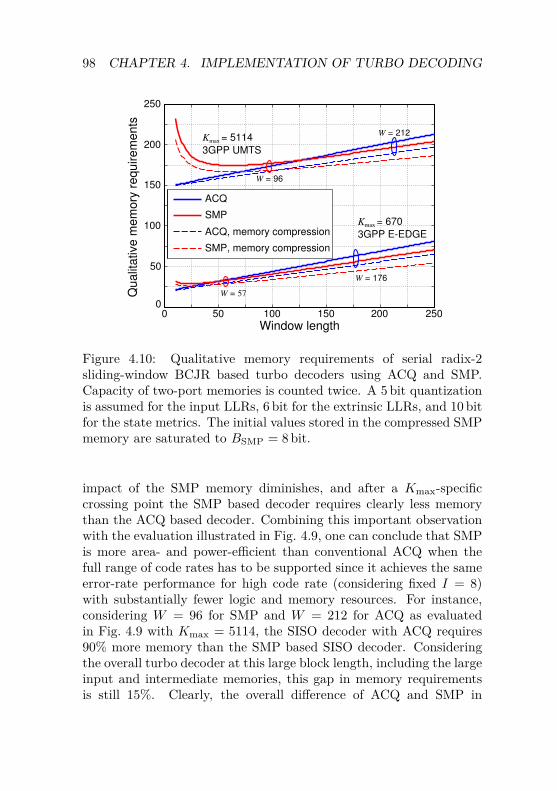
98 CHAPTER 4. IMPLEMENTATION OF TURBO DECODING
0 50 100 150 200 2500
50
100
150
200
250
Window length
Qu
alit
ative
me
mo
ry r
eq
uire
me
nts
ACQ
SMP
ACQ, memory compression
SMP, memory compression
Kmax
= 5114
3GPP UMTS
Kmax
= 670
3GPP E-EDGE
W = 96
W = 212
W = 176
W = 57
Figure 4.10: Qualitative memory requirements of serial radix-2sliding-window BCJR based turbo decoders using ACQ and SMP.Capacity of two-port memories is counted twice. A 5 bit quantizationis assumed for the input LLRs, 6 bit for the extrinsic LLRs, and 10 bitfor the state metrics. The initial values stored in the compressed SMPmemory are saturated to BSMP = 8 bit.
impact of the SMP memory diminishes, and after a Kmax-specificcrossing point the SMP based decoder requires clearly less memorythan the ACQ based decoder. Combining this important observationwith the evaluation illustrated in Fig. 4.9, one can conclude that SMPis more area- and power-efficient than conventional ACQ when thefull range of code rates has to be supported since it achieves the sameerror-rate performance for high code rate (considering fixed I = 8)with substantially fewer logic and memory resources. For instance,considering W = 96 for SMP and W = 212 for ACQ as evaluatedin Fig. 4.9 with Kmax = 5114, the SISO decoder with ACQ requires90% more memory than the SMP based SISO decoder. Consideringthe overall turbo decoder at this large block length, including the largeinput and intermediate memories, this gap in memory requirementsis still 15%. Clearly, the overall difference of ACQ and SMP in
4.3. SERIAL TURBO DECODERS 99
terms of memory requirements becomes more pronounced for smallerKmax, i.e., smaller input and intermediate memories. In particular,for Kmax = 670 with window lengths4 W = 57 for SMP and W = 176for ACQ, the overall ACQ based turbo decoder requires 92% morememory than the decoder with SMP.
The dashed curves in Fig. 4.10 show the qualitative memory re-quirements considering the proposed compression techniques for theAlpha and SMP memories introduced in Sec. 4.2.1. As expected,the Alpha memory compression has high impact on the memory re-quirements for large window lengths, whereas the SMP memory com-pression is especially useful for smaller window lengths. Consideringonly the SISO decoders, the Alpha memory compression reduces thememory requirements of ACQ by 25% at W = 212. The requirementsof SMP using both Alpha and SMP memory compression are reducedby even 30% at W = 96. Hence, the proposed compression techniquessignificantly reduce the memory requirements of both SISO decodersand therefore generally qualify as efficient approaches to improve thearea efficiency of flexible serial radix-2 turbo decoders.
Latency Recall from Sec. 4.2.1 that the SISO-decoder latency forSMP is λSMP = W , whereas for ACQ it is λACQ = 2W . Hence,the ACQ based turbo decoder suffers from a significant latency athigh code rate, considering the exploding window lengths requiredat this operating condition. Due to the large latency, the turbodecoder requires more cycles to decode the code block (see (4.1)),which generally reduces the throughput and, thus, degrades the siliconefficiency of the decoder. Obviously, for a serial decoder, this issueis more pronounced for smaller block lengths. For Kmax = 5114, forinstance, the SISO-decoder latency in the ACQ based turbo decoderamounts to less than 9% of the block length and, thus, can be ne-glected. For Kmax = 670, on the other hand, the ACQ based turbodecoder requires roughly 50% more clock cycles per code block dueto latency, which results in highly inefficient operation. For the serialturbo decoder with SMP, the impact of the latency can be neglectedfor both considered Kmax.
4The optimal window lengths for Kmax = 670 have been evaluated in [25].
100 CHAPTER 4. IMPLEMENTATION OF TURBO DECODING
SOVA based versus BCJR based Turbo Decoders
Similar to SMP, the proposed SOVA based turbo decoder only re-quires two sets of ACS units and only one two-port address memoryto buffer AL + U interleaved addresses. As shown in Fig. 4.8, ourSOVA decoder heavily relies on shift-registers and flip-flop based REcomputations. While this structure proves to be efficient for thesmall AL and U required at low code rate, the latency, silicon area,and power consumption are expected to explode for the large ALand U required to support high code rate without serious error-rateperformance degradation. The two considered BCJR decoders, on theother hand, are based on memories which can be implemented witharea-economic SRAM macrocells.
To quantify the exploding silicon area of SOVA decoders support-ing the full range of code rates, consider our high-speed ASIC pro-totype described in the second column of Table 4.1. Recall that thisimplementation has been optimized for unpunctured operation withAL = 30, U = 21, and U1 = 6. Considering now the operation at highcode rate for Kmax = 5114, the acquisition length must be increasedto AL = 230 (see Fig. 4.9). Regarding the other two parameters, oursimulations have shown that U = 126, and U1 = 36 result in a goodperformance/complexity trade-off. This set of parameters results inan estimated active cell area of 135 kGE, which corresponds to a morethan 4× area increase with respect to the reference implementation.It is expected that the power consumption increases with similar rate.This observation lets us conclude that the SOVA is in general ratherunsuited for the implementation of flexible turbo decoders.
4.3.2 VLSI Implementation Results for UMTS
To underline the results of the previous qualitative architecture study,the ACQ and SMP based turbo decoders optimized for 3GPP UMTSand its enhancements [38] with Kmax = 5114 have been implementedin 180 nm CMOS. All memories and address buffers are realized withSRAM macrocells. The two input LLRs are quantized with 5 bit,whereas a 6 bit quantization is used for the extrinsic and a-priori LLRs.The state metrics are represented with BSM = 10 bit. Furthermore,
4.3. SERIAL TURBO DECODERS 101
0 0.5 1 1.5 2 2.5 3 3.5 4 4.50
0.2
0.4
0.6
0.8
1
1.2
32
128
212
292
16
96
150
100
1660
SNR loss [dB]
ACQ
SMP
ACQ, memory compression
SMP, memory compression
SOVA
0.1 0.15 0.2 0.25 0.3
0.4
0.5
0.6
0.7
212
270
292
6080
96
150
292
212
270
292
608096
150
Active
SIS
O d
eco
de
r a
rea
[m
m2]
no
n-w
ind
ow
ed
ma
x-lo
g-B
CJR
292
AL=230U=126
U1=36
AL=30U=21
U1=6
292
150
0.05
Figure 4.11: Silicon area versus error-rate performance trade-offs ofSISO decoders. The numbers next to the markers correspond to theemployed window length.
the hard-estimates bk generated by the SISO decoder in every half-iteration are stored along with the extrinsic LLRs in the intermediatememory. This new approach allows one to save a dedicated outputbuffer at the cost of a slightly increased intermediate memory size [90].The interleaver used in the address generator is based on the existinginterleaver design presented in [19,75] which realizes the complicatedblock interleaving specified for UMTS highly efficiently by dividingthe address generation into a preparatory stage (executed during thefirst half-iteration) and an on-the-fly address computation stage thatsupports all block lengths specified by the standard.
SISO Decoder Trade-off Analysis
The choice of the window length mainly affects the SISO decoderimplementation. To study the quantitative impact of the windowlength on the SISO decoder area with respect to the associated turbo
102 CHAPTER 4. IMPLEMENTATION OF TURBO DECODING
decoder error-rate performance, an area/performance trade-off analy-sis has been carried out. The analysis bases on post-layout implemen-tation results5 and has been conducted at high code rate R = 0.95,which is the worst-case operating condition that determines the over-all complexity of flexible turbo decoders. The results are shownin Fig. 4.11 which plots the active SISO decoder cell area for differentwindow lengths with and without memory compression over the actualfixed-point error-rate performance of the corresponding serial turbodecoder. The error-rate performance is characterized by the SNR op-erating point required to achieve a BLER of 10−2 at I = 8 iterations.This operating point is a typical performance requirement in recentcellular standards. Note that the operating points in Fig. 4.11 arenormalized with respect to the operating point of the non-windowedmax-log-BCJR decoder with floating-point arithmetics.
Interestingly, the curves nicely reflect the window-dependent mem-ory requirements discussed in Fig. 4.10. They also highlight the con-siderably better area efficiency of SMP compared to ACQ when highcode rates must be supported with small error-rate performance loss.Observe for the considered setup that the choice of W = 96 andW = 212 for SMP and ACQ, respectively, results in a good complex-ity/performance trade-off. For larger W , the silicon area of both de-coders inflates while the gains in terms of performance are diminishing.Most published stand-alone SISO decoders and serial turbo decodersare based on ACQ with window lengths between 32 and 40 (see,e.g., [72–75, 94]). As clearly shown in Fig. 4.11, this conventionalconfiguration leads to an unacceptably large performance loss forhigh code rate. Optimizing this configuration for high code rate, i.e.,changing the window length from 32 to 212, comes at the expense ofan estimated 1.7× area increase. The SISO decoder with SMP, on theother hand, supports the high code rate with an active area that is
5The analysis is based on reference implementations at specific window lengthsand operating clock frequency of 340 MHz. The implementation results for otherwindow lengths have been estimated assuming that the choice of W only affectsthe area and power consumption of the memories, while the area and power of theremaining blocks as well as the maximum clock frequency remain unchanged.In order to obtain accurate area and power data for the memories, a linearinterpolation model has been used relying on a large set of datasheets for manydifferent memory dimensions generated by the SRAM macrocell compiler providedby the target design kit [90].
4.3. SERIAL TURBO DECODERS 103
only slightly larger than the area of the non-optimized ACQ decoderat W = 32. Comparing the SMP and ACQ based SISO decoder typesat W = 96 and W = 212, respectively, shows that the SMP baseddecoder requires substantially 30% less silicon area than the SISOdecoder with ACQ. The lower silicon area of SMP is a consequenceof both lower memory overhead and lower logic overhead due to theomitted dummy backward SMU.
Interestingly, observe from Fig. 4.11 that the proposed memorycompression techniques for the Alpha and SMP memories have asignificant impact on the overall SISO decoder area. In particular,at the optimal window lengths, the area of both SISO decoders isreduced by more than 10% when these compression techniques areemployed.
For the sake of completeness, our SOVA based SISO decoder isalso considered in Fig. 4.11. Optimized for unpunctured operation,the SOVA decoder requires fewer area resources than the other twodecoders. Optimized for high code rate, on the other hand, the SOVAdecoder occupies about 2× the area used by the ACQ based SISOdecoder. Even when the area increase in the first RE unit REU1 isneglected, the large amount of shift registers and the inflated hardwareresources required to track the concurrent paths in REU2 increase theoriginal cell area by a factor of 2.4×. This observation underlines ourpreviously noted conclusion that SOVA based turbo decoders are ill-suited when the full range of code rates has to be supported — even ifthe more area-economic memory trace-back approach was consideredto implement the ML trace-back.
Turbo Decoder Implementation Results
The ACQ and SMP based turbo decoders have been implemented6
with window lengths W = 212 and W = 96, respectively. The cor-responding post-layout implementation results are summarized in thesecond and third column of Table 4.4. Both turbo decoders achievea maximum clock frequency of 340 MHz, which translates into a de-coding throughput of about 20 Mbps at I = 8 iterations. Note thatthe throughput of the ACQ based decoder is slightly smaller due to
6The memory compression techniques have not been included in the final turbodecoder implementations.
104 CHAPTER 4. IMPLEMENTATION OF TURBO DECODING
the associated high SISO-decoder latency. However, both decodersclearly exceed the 14.4 Mbps requirements of HSPA. When consideringmore recent technology nodes such as the 65 nm node, the presenteddecoders would also easily achieve the peak throughput requirementsof HSPA+.
The detailed cell-area breakdown of the two decoders is summa-rized in Table 4.2. The ACQ and SMP based turbo decoders require155 kbit and 137 kbit of SRAM macrocells, where a share of 23 kbitand 18 kbit are used by the two BCJR decoders. As expected, thelarge input and intermediate memories required for Kmax = 5114amount to a large fraction (roughly 50%) of the overall turbo decoderarea and therefore mask the area difference of the two BCJR decodertypes to a great extent. Nevertheless, the turbo decoder based onSMP is 14% smaller than the ACQ based turbo decoder. Withoutthe large input memory, the area difference is even 20%. Observefrom Table 4.2 that the address generators contribute to the overallarea difference in addition to the two BCJR decoders. In particular,the address generator in the turbo decoder with SMP is 25% smalleras a consequence of the smaller address buffers.
According to our post-layout simulations, the BCJR decoder withSMP consumes roughly 20% less power, which is a direct consequenceof the omitted dummy backward SMU and the reduced memory di-mensions. Considering the overall turbo decoder, the gap betweenSMP and ACQ in terms of energy per information bit per iterationis more than 10% as shown in Table 4.4. Recall, however, that ACQexhibits a higher convergence speed than SMP. Due to this reason,the ACQ based turbo decoder slightly outperforms the other decodertype in terms of average energy per information bit for larger SNRswhen early termination is considered [25,90].
Comparison with prior-art UMTS turbo decoders Table 4.4provides comparison with a selection of the best stand-alone UMTSturbo decoder ASICs found in the open literature. We emphasizethat all these turbo decoders do not support high code rate (i.e.,they exhibit a considerable performance degradation) as they are allbased on ACQ with small window lengths between 30 and 40. Thetwo presented decoders, on the other hand, are fully flexible not only
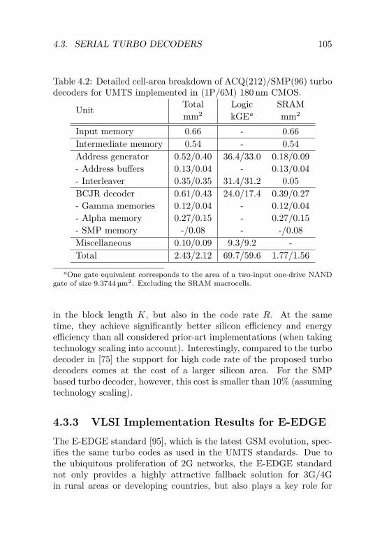
4.3. SERIAL TURBO DECODERS 105
Table 4.2: Detailed cell-area breakdown of ACQ(212)/SMP(96) turbodecoders for UMTS implemented in (1P/6M) 180 nm CMOS.
Unit Total Logic SRAMmm2 kGEa mm2
Input memory 0.66 - 0.66Intermediate memory 0.54 - 0.54Address generator 0.52/0.40 36.4/33.0 0.18/0.09- Address buffers 0.13/0.04 - 0.13/0.04- Interleaver 0.35/0.35 31.4/31.2 0.05BCJR decoder 0.61/0.43 24.0/17.4 0.39/0.27- Gamma memories 0.12/0.04 - 0.12/0.04- Alpha memory 0.27/0.15 - 0.27/0.15- SMP memory -/0.08 - -/0.08Miscellaneous 0.10/0.09 9.3/9.2 -Total 2.43/2.12 69.7/59.6 1.77/1.56
aOne gate equivalent corresponds to the area of a two-input one-drive NANDgate of size 9.3744 µm2. Excluding the SRAM macrocells.
in the block length K, but also in the code rate R. At the sametime, they achieve significantly better silicon efficiency and energyefficiency than all considered prior-art implementations (when takingtechnology scaling into account). Interestingly, compared to the turbodecoder in [75] the support for high code rate of the proposed turbodecoders comes at the cost of a larger silicon area. For the SMPbased turbo decoder, however, this cost is smaller than 10% (assumingtechnology scaling).
4.3.3 VLSI Implementation Results for E-EDGEThe E-EDGE standard [95], which is the latest GSM evolution, spec-ifies the same turbo codes as used in the UMTS standards. Due tothe ubiquitous proliferation of 2G networks, the E-EDGE standardnot only provides a highly attractive fallback solution for 3G/4Gin rural areas or developing countries, but also plays a key role for
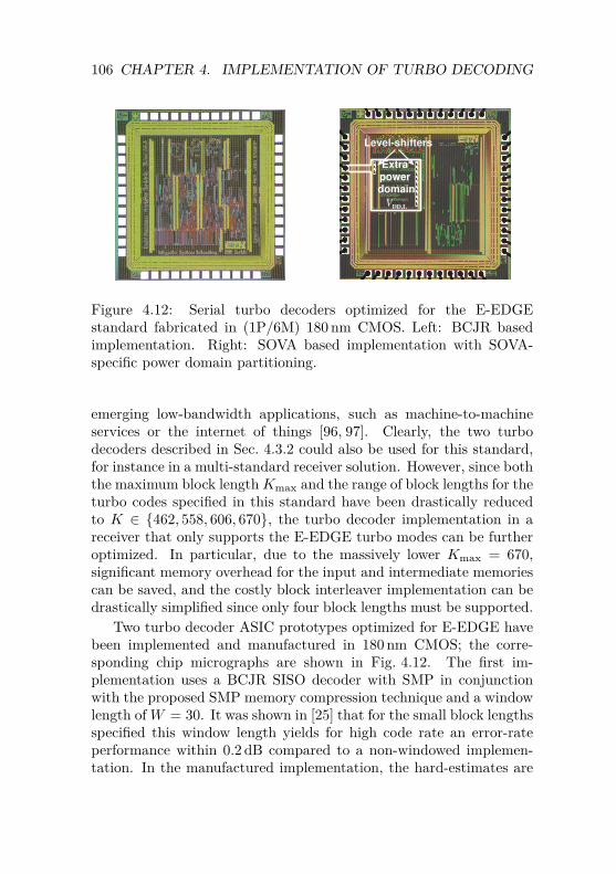
106 CHAPTER 4. IMPLEMENTATION OF TURBO DECODING
Extra power domain
VDD,L
Level-shifters
Figure 4.12: Serial turbo decoders optimized for the E-EDGEstandard fabricated in (1P/6M) 180 nm CMOS. Left: BCJR basedimplementation. Right: SOVA based implementation with SOVA-specific power domain partitioning.
emerging low-bandwidth applications, such as machine-to-machineservices or the internet of things [96, 97]. Clearly, the two turbodecoders described in Sec. 4.3.2 could also be used for this standard,for instance in a multi-standard receiver solution. However, since boththe maximum block length Kmax and the range of block lengths for theturbo codes specified in this standard have been drastically reducedto K ∈ {462, 558, 606, 670}, the turbo decoder implementation in areceiver that only supports the E-EDGE turbo modes can be furtheroptimized. In particular, due to the massively lower Kmax = 670,significant memory overhead for the input and intermediate memoriescan be saved, and the costly block interleaver implementation can bedrastically simplified since only four block lengths must be supported.
Two turbo decoder ASIC prototypes optimized for E-EDGE havebeen implemented and manufactured in 180 nm CMOS; the corre-sponding chip micrographs are shown in Fig. 4.12. The first im-plementation uses a BCJR SISO decoder with SMP in conjunctionwith the proposed SMP memory compression technique and a windowlength of W = 30. It was shown in [25] that for the small block lengthsspecified this window length yields for high code rate an error-rateperformance within 0.2 dB compared to a non-windowed implemen-tation. In the manufactured implementation, the hard-estimates are
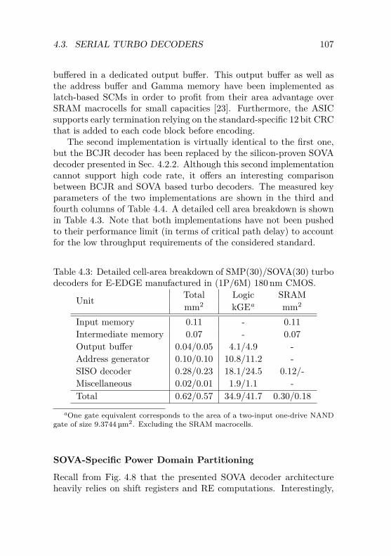
4.3. SERIAL TURBO DECODERS 107
buffered in a dedicated output buffer. This output buffer as well asthe address buffer and Gamma memory have been implemented aslatch-based SCMs in order to profit from their area advantage overSRAM macrocells for small capacities [23]. Furthermore, the ASICsupports early termination relying on the standard-specific 12 bit CRCthat is added to each code block before encoding.
The second implementation is virtually identical to the first one,but the BCJR decoder has been replaced by the silicon-proven SOVAdecoder presented in Sec. 4.2.2. Although this second implementationcannot support high code rate, it offers an interesting comparisonbetween BCJR and SOVA based turbo decoders. The measured keyparameters of the two implementations are shown in the third andfourth columns of Table 4.4. A detailed cell area breakdown is shownin Table 4.3. Note that both implementations have not been pushedto their performance limit (in terms of critical path delay) to accountfor the low throughput requirements of the considered standard.
Table 4.3: Detailed cell-area breakdown of SMP(30)/SOVA(30) turbodecoders for E-EDGE manufactured in (1P/6M) 180 nm CMOS.
Unit Total Logic SRAMmm2 kGEa mm2
Input memory 0.11 - 0.11Intermediate memory 0.07 - 0.07Output buffer 0.04/0.05 4.1/4.9 -Address generator 0.10/0.10 10.8/11.2 -SISO decoder 0.28/0.23 18.1/24.5 0.12/-Miscellaneous 0.02/0.01 1.9/1.1 -Total 0.62/0.57 34.9/41.7 0.30/0.18
aOne gate equivalent corresponds to the area of a two-input one-drive NANDgate of size 9.3744 µm2. Excluding the SRAM macrocells.
SOVA-Specific Power Domain Partitioning
Recall from Fig. 4.8 that the presented SOVA decoder architectureheavily relies on shift registers and RE computations. Interestingly,
108 CHAPTER 4. IMPLEMENTATION OF TURBO DECODING
the simple structure of our RE units amounts to short signal-pathdelays — given by the propagation delay of up to four 2-to-1 multiplex-ers in our specific implementation. These paths are in general muchshorter than the ones found in the recursive ACS units. In our specificimplementation, synthesis results in the target technology show thatthe longest paths in our ACS units are roughly 2.4× as long7 as theones in our RE units. From a power perspective, it is thus inefficientto operate these short signal paths at the same operating voltageas the ACS circuits. Therefore, we propose to integrate REU1 andREU2 as well as the two shift registers in a separate power domain.This extra domain can be operated at lower voltage (VDD,L) than thenominal supply voltage (VDD) without degrading the overall criticalpath, allowing us to reduce power consumption through voltage scal-ing without sacrificing any throughput.
In the middle-left part of the chip micrograph shown in Fig. 4.12,one can recognize the extra voltage region surrounded by a separatepower ring that powers the RE circuits and shift registers, whichtogether amount to 55% of the overall SOVA decoder cell area. Toprovide proper voltage-level conversion for signals passing from VDD,Lto VDD, level-shifters have been placed at the boundary of the twodomains. The area overhead of this SOVA-specific power domainpartitioning (including the 104 level-shifters and the additional powerring) is less than 5% of the overall core area. Fig. 4.13 shows themeasured power consumption of our SOVA based turbo decoder overoperating clock frequency.
Block-level voltage scaling The first curve (square markers) isassociated with the scenario where both voltages VDD and VDD,L arescaled identically. This case corresponds to the standard practicewhere all circuit blocks are powered by a single supply voltage. As ex-pected, when the decoder is operated at its maximum clock frequency,no voltage scaling can be performed as correct functionality could notbe maintained otherwise. Only for lower operating frequencies, theresulting headroom in circuit speed permits the voltage to be reducedto save power. In this particular implementation, the voltage VDD
7The delay estimations include the propagation delay and setup time of theflip-flops.
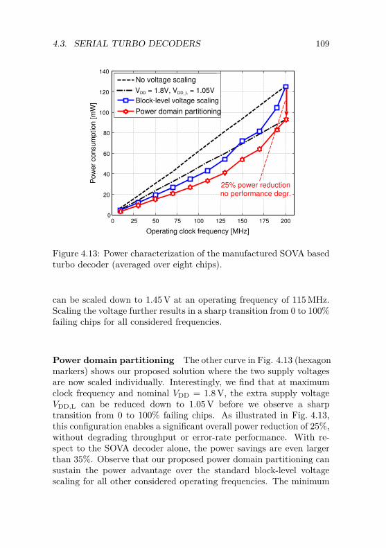
4.3. SERIAL TURBO DECODERS 109
0 25 50 75 100 125 150 175 2000
20
40
60
80
100
120
140
Operating clock frequency [MHz]
Po
we
r co
nsu
mp
tio
n [
mW
]
No voltage scaling
Block-level voltage scaling
Power domain partitioning
25% power reductionno performance degr.
VDD = 1.8V, VDD_L = 1.05V
Figure 4.13: Power characterization of the manufactured SOVA basedturbo decoder (averaged over eight chips).
can be scaled down to 1.45 V at an operating frequency of 115 MHz.Scaling the voltage further results in a sharp transition from 0 to 100%failing chips for all considered frequencies.
Power domain partitioning The other curve in Fig. 4.13 (hexagonmarkers) shows our proposed solution where the two supply voltagesare now scaled individually. Interestingly, we find that at maximumclock frequency and nominal VDD = 1.8 V, the extra supply voltageVDD,L can be reduced down to 1.05 V before we observe a sharptransition from 0 to 100% failing chips. As illustrated in Fig. 4.13,this configuration enables a significant overall power reduction of 25%,without degrading throughput or error-rate performance. With re-spect to the SOVA decoder alone, the power savings are even largerthan 35%. Observe that our proposed power domain partitioning cansustain the power advantage over the standard block-level voltagescaling for all other considered operating frequencies. The minimum
110 CHAPTER 4. IMPLEMENTATION OF TURBO DECODING
measured extra supply voltage is VDD,L = 0.95 V, reached at anoperating frequency of 180 MHz.
Comparison
As can be observed in Table 4.4, the presented E-EDGE turbo de-coders generally achieve better energy efficiency and require signifi-cantly less silicon area than the UMTS decoders. This lower imple-mentation complexity of E-EDGE turbo decoders is a direct conse-quence of the reduced memory overhead and the less complex in-terleaver implementation. Recall that the presented SOVA basedturbo decoder only supports low code rates, and that the costs interms of silicon area required to support the full code rate range areunacceptably high. However, if only operation at low code rate isconsidered, the SOVA based turbo decoder is highly competitive. Infact, it can be seen that this decoder provides better energy efficiency(at nominal supply voltage) than the BCJR based E-EDGE turbodecoder and occupies less cell area8 as can be observed from Table 4.3.Using the described SOVA-specific power domain partitioning onecan perform voltage scaling even at maximum clock frequency, whichwidens the gap in energy efficiency compared to the BCJR based im-plementation to substantial 35%. We emphasize that turbo decodersbased on BCJR cannot profit from such a power domain partitioningin general since they exhibit more balanced signal-path delays thanSOVA decoders as they mainly consist of ACS logic and memories.
8Due to multi-project-wafer fabrication constraints, the reduced cell area(shown in Table 4.3) is not reflected in the total core area (shown in Table 4.4).
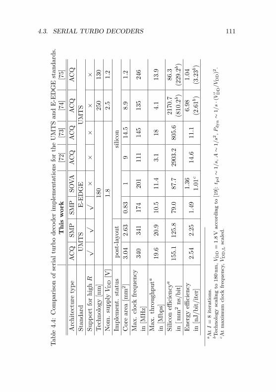
4.3. SERIAL TURBO DECODERS 111
Tabl
e4.
4:C
ompa
rison
ofse
rialt
urbo
deco
der
impl
emen
tatio
nsfo
rth
eU
MT
San
dE-
EDG
Est
anda
rds.
Thi
sw
ork
[72]
[73]
[74]
[75]
Arc
hite
ctur
ety
peA
CQ
SMP
SMP
SOVA
AC
QA
CQ
AC
QA
CQ
Stan
dard
UM
TS
E-ED
GE
UM
TS
Supp
ort
for
high
R√
√√
××
××
×Te
chno
logy
[nm
]18
025
013
0N
om.
supp
lyV
DD
[V]
1.8
2.5
1.2
Impl
emen
t.st
atus
post
-layo
utsil
icon
Cor
ear
ea[m
m2 ]
3.04
2.63
0.83
19
14.5
8.9
1.2
Max
.cl
ock
frequ
ency
340
341
174
201
111
145
135
246
in[M
Hz]
Max
.th
roug
hput
a19
.620
.910
.511
.43.
118
4.1
13.9
in[M
bps]
Silic
oneffi
cien
cya
155.
112
5.8
79.0
87.7
2903
.280
5.6
2170
.786
.3in
[mm
2ns
/bit]
(810
.2b )
(229
.2b)
Ener
gyeffi
cien
cy2.
542.
251.
491.
3614
.611
.16.
981.
04in
[nJ/
bit/
iter]
1.01
c(2
.61b
)(3
.23b
)a A
tI
=8
itera
tions
.b T
echn
olog
ysc
alin
gto
180n
m,V
DD
=1.
8Vac
cord
ing
to[1
9]:t p
d∼
1/s,A∼
1/s2
,Pdy
n∼
1/s·(V′ D
D/V
DD
)2.
c At
max
imum
cloc
kfr
eque
ncy,V
DD
,Lsc
aled
.
112 CHAPTER 4. IMPLEMENTATION OF TURBO DECODING
4.4 Design of Subblock-ParallelTurbo Decoders
We next consider the subblock-parallel turbo decoder architectureillustrated in the lower part of Fig. 4.1 and focus on the sliding-window BCJR SISO decoder architectures presented in Sec. 4.2 andthe turbo codes specified for LTE and LTE-A with Kmax = 6144 [39].The SOVA is not considered in the ensuing discussion due to itspoor area efficiency when high code rates have to be supported (referto Sec. 4.3).
The Need for a Constrained Throughput Evaluation
The ultimate performance metric of subblock-parallel turbo decodersis throughput. In order to maximize the turbo decoder throughputin (4.1) and to minimize the impact of the parallel turbo-decoderpredicament illustrated in Fig. 4.2 one would preferably choose bothI and the SISO-decoder latency λ (i.e., the window length W ) assmall as possible. However, it has been shown previously that thechoice of these parameters strongly affects the BER performance of theturbo decoder, especially for high code rate. Typically, I and W arefixed parameters that are chosen large enough to allow for a saturatedBER performance of the decoder (as we have done for the serial de-coders discussed in Sec. 4.3). This approach is not necessarily optimalin terms of throughput under a given BER performance constraint,which is usually specified in wireless communication standards. Fur-thermore, each SISO decoder architecture has its own distinct BERperformance characteristic in I and W that must be observed whencomparing the throughput of different architectures.
We next introduce a novel framework that allows for a systematicand unified throughput evaluation of sliding-window turbo decodersunder a fixed BER performance constraint. Using this framework asa basis, a comparison of existing architectures follows, revealing thatthe method employed to initialize the window boundaries inside BCJRbased SISO decoders has in general a strong impact on the throughputof subblock-parallel turbo decoders. Based on these findings, a newSISO decoder architecture will be introduced, combining the strengths
4.4. SUBBLOCK-PARALLEL TURBO DECODERS 113
of ACQ and SMP and leading to significantly higher throughput forall code rates while achieving better silicon efficiency.
4.4.1 Constrained Throughput EvaluationConsider a sliding-window P > 1 subblock-parallel turbo decoderperforming Ih half-iterations with SISO decoder architecture A andarchitecture-specific latency λA(W ). We refer to this specific turbodecoder as AP . Recall from (4.1) that the throughput θP (Ih, λA(W ))of the decoder depends on Ih and W . We assume data transmis-sion over some propagation channel at a target signal-to-noise ratioSNR∗ and let BERAP (Ih,W,SNR∗) be the corresponding BER ofthe decoder. In order to make the throughput performance of thedecoder comparable to the one of other decoders, we impose a targetbit error-rate BER∗ at the target SNR and maximize the decoderthroughput under this target BER performance constraint. Morespecifically, we define the constrained maximum throughput of theturbo decoder AP under the performance constraint BER∗ as theresult of the constrained maximization problem
ΘAP ,maxW ,Ih
θP (Ih, λA(W ))
subject to BERAP (Ih, W ,SNR∗) ≤ BER∗,(4.3)
where we let the maximization run over all window lengths W ∈ SW ,SW = {r, 2r, 3r, . . . ,Wmax}9 and all Ih ∈ SIh
= {1, 2, 3, . . . , Ih,max}.The choice of Wmax ≤ KP can be influenced by some constrainton the silicon area of the turbo decoder implementation or by otherpractical considerations. Similarly, Ih,max can account for a specificmaximum latency constraint of the decoder. The target BER perfor-mance BER∗ and the corresponding target signal-to-noise ratio SNR∗can be chosen following some standard specifications or according tothe performance of a reference decoder.
The constrained maximization in (4.3) enables an optimal trade-offbetween window length W and half-iterations Ih so that the turbodecoder throughput is maximized under the target BER performance
9For practical reasons, the window length in radix-2r turbo decoder implemen-tations is typically chosen to be a multiple of r (see, e.g., [80]).
114 CHAPTER 4. IMPLEMENTATION OF TURBO DECODING
constraint. Furthermore, the application of a reference constraintallows for a fair comparison of different SISO decoder architectures.Note, however, that the constrained maximization in (4.3) maximizesthe decoder throughput for a fixed P only. Hence, the constrainedmaximization must be performed for all P of interest. The finalchoice of P is up to the designer. This choice can be motivatedby maximizing the overall throughput (which typically results in thelargest considered P ) or by specific constraints on the silicon area ofthe implementation.
Solving the Constrained Maximization Problem
In order to solve the constrained maximization problem in (4.3), con-sider first the 2-dimensional W -Ih plane and split it into two disjointsets R+
AP and R−AP with
R+AP = {(W , Ih) : BERAP (Ih, W ,SNR∗) ≤ BER∗},R−AP = {(W , Ih) : BERAP (Ih, W ,SNR∗) > BER∗}.
(4.4)
Practically, we achieve the splitting by means of Monte-Carlo sim-ulations (averaged over propagation-channel realizations), which wefirst perform to evaluate the bit error-rate BERAP (Ih, W ,SNR∗) ofthe decoder at the target SNR for all W ∈ SW and Ih ∈ SIh
. In asecond step, we then distribute all pairs (W , Ih) among the two setsaccording to (4.4). To this end, for each fixed W , the two conditionsin (4.4) are checked for all Ih in ascending order. When the BERconstraint is met for a specific half-iteration number it is assumedthat it is also met for all larger Ih. Per Monte-Carlo simulation, thedecoder is run with a fixed W for Ih,max iterations and the BER resultsare extracted for all Ih ≤ Ih,max. Hence, we require to perform only|SW | Monte-Carlo simulations per decoder AP , where |SW | denotesthe number of elements in SW .
By definition, none of the pairs (W , Ih) in R−AP are valid for thethroughput maximization in (4.3) as they do not satisfy the BERperformance constraint. On the other hand, all pairs inR+
AP are valid.However, most of these pairs can be excluded from the maximization.In fact, only the pairs on the boundary of R+
AP defined as
B(R+AP ) = {(W , Ih) ∈ R+
AP : (W , Ih − 1) /∈ R+AP } (4.5)
4.4. SUBBLOCK-PARALLEL TURBO DECODERS 115
need to be considered, since for each valid pair (W , Ih) that does notlie on this boundary, there exists at least one other valid pair (W , I ′h)with I ′h < Ih, which leads to higher throughput due to the relationθP ∝ 1/Ih. Thus, the constrained maximization problem simplifies tomaximizing the throughput over this boundary, i.e.,
ΘAP = max(W ,Ih)∈B(R+
AP)θP (Ih, λA(W )). (4.6)
Finally, we define the optimal window length W ∗ and the optimalnumber of half-iterations I∗h for decoder AP as
(W ∗, I∗h) , arg max(W ,Ih)∈B(R+
AP)θP (Ih, λA(W )). (4.7)
4.4.2 Throughput Evaluation ExampleIn order to illustrate the proposed constrained throughput evaluation,the example of subblock-parallel turbo decoders based on ACQ andSMP is considered for the two corner code rates R = RTC = 1/3and R = 0.95, respectively. For the sake of clarity we limit thediscussion to the example value P = 16. In Sec. 4.4.3 results for othervalues of P are shown as well. We consider the maximum block lengthK = 6144 and, thus, KP = 384. Transmission over an AWGN channelis assumed in line with the system model introduced in Chapter 2.
Reference Configuration
For R = RTC, we choose as reference decoder a serial P = 1 radix-4 turbo decoder based on ACQ with Ih = 12 and W = 32. ForR = 0.95, on the other hand, a serial radix-4 turbo decoder based onSMP with Ih = 12 and W = 64 is considered.10 We set the targetbit error-rate BER∗ = 10−5 and choose the target signal-to-noise ratioSNR∗ individually for the two code rates so that the correspondingreference decoders exactly meet the target BER. Note that the chosentarget BER corresponds to a block error-rate of about 10−2, which isa typical performance requirement in recent wireless standards. We
10These are typical configurations reported in recent publications of subblock-parallel turbo decoder implementations (e.g., [80, 81]).
116 CHAPTER 4. IMPLEMENTATION OF TURBO DECODING
will use this reference configuration for all throughput evaluationspresented in the remainder of this chapter.
SISO-decoder Latency versus Half-Iterations
Fig. 4.14(a) illustrates the W -Ih plane as defined in (4.4) and depictsthe resulting boundaries B(R+
ACQP ) and B(R+SMPP ) from (4.5) for
R = 0.95. Recall that only the pairs on these two boundaries haveto be considered during the throughput optimization. The otherpairs either lie in R− and, thus, do not achieve the target BER orare valid, but outperformed in terms of throughput by other pairswith smaller Ih and/or smaller W . Interestingly, Fig. 4.14(a) revealsa trade-off between the window length (or SISO-decoder latency)and the number of half-iterations Ih required to achieve the BERperformance constraint. It can be observed that the SISO-decoderlatency can be reduced at the cost of more half-iterations requiredto achieve the target BER. This trade-off leads to the characteris-tic throughput curves in Fig. 4.14(b) where the resulting normalizedthroughput θP,N (Ih, λA(W )) with (Ih,W ) ∈ B(R+
AP ) is shown forboth decoders. Note that the peak value of these curves correspondsto the normalized maximum constrained throughput ΘAP ,N .
Throughput Comparison
Table 4.5 shows the normalized constrained maximum throughputΘAP ,N for Ih,max = 24 and the maximum possible Wmax = KP = 384.In addition, a smaller Wmax = 32 is considered as well. The choiceof a smaller Wmax allows one to indirectly limit the silicon area ofcorresponding implementations.
Low code rate R = RTC From Table 4.5 it can be observed thatthe turbo decoder based on ACQ generally requires fewer half-iterationsto achieve the target BER performance and, thus, outperforms theSMP based architecture in terms of throughput. As already pointedout in Sec. 4.2, this can be explained by the fact that the SMPbased architecture operates with uninitialized backward state metricsduring the first two half-iterations, leading to a slower convergencespeed. Furthermore, we find that for this low code rate, the maximum
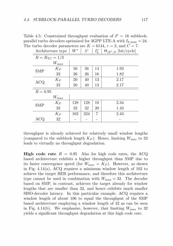
4.4. SUBBLOCK-PARALLEL TURBO DECODERS 117
Table 4.5: Constrained throughput evaluation of P = 16 subblock-parallel turbo decoders optimized for 3GPP LTE-A with Ih,max = 24.The turbo decoder parameters are K = 6144, r = 2, and C = 7.
Architecture type W ∗ λ∗ I∗h ΘAP ,N [bit/cycle]R = RTC = 1/3
Wmax
SMP KP 56 56 14 1.9332 26 26 16 1.82
ACQ KP 20 40 13 2.1732 20 40 13 2.17
R = 0.95Wmax
SMP KP 128 128 10 2.3432 32 32 20 1.43
ACQKP 162 324 7 2.4332 - - - -
throughput is already achieved for relatively small window lengths(compared to the subblock length KP ). Hence, limiting Wmax to 32leads to virtually no throughput degradation.
High code rate R = 0.95 Also for high code rates, the ACQbased architecture exhibits a higher throughput than SMP due toits faster convergence speed (for Wmax = KP ). However, as shownin Fig. 4.14(a), ACQ requires a minimum window length of 102 toachieve the target BER performance, and therefore this architecturetype cannot be used in combination with Wmax = 32. The decoderbased on SMP, in contrast, achieves the target already for windowlengths that are smaller than 32, and hence exhibits much smallerSISO-decoder latency. In this particular example, ACQ requires awindow length of about 106 to equal the throughput of the SMPbased architecture employing a window length of 32 as can be seenin Fig. 4.14(b). We emphasize, however, that limiting Wmax to 32yields a significant throughput degradation at this high code rate.
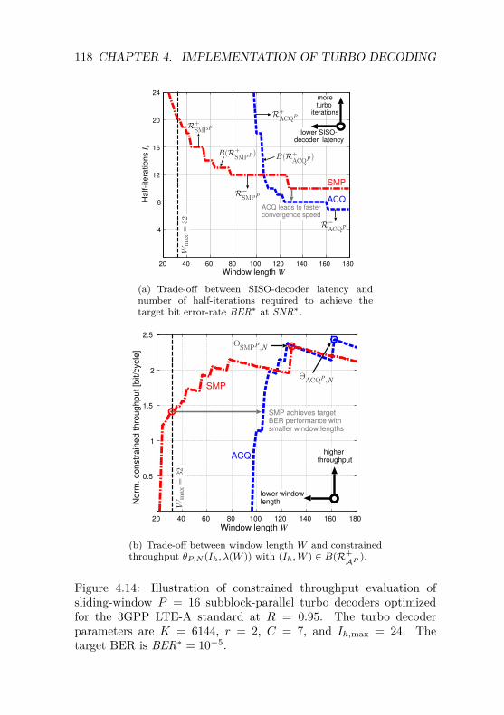
118 CHAPTER 4. IMPLEMENTATION OF TURBO DECODING
20 40 60 80 100 120 140 160 180
4
8
12
16
20
24
Window length W
Ha
lf-ite
ratio
ns I
h
B(R+SMPP
)
R+SMPP
R−SMPP
B(R+ACQP )
R−ACQP
R+ACQP
ACQ
SMP
lower SISO-decoder latency
moreturbo
iterations
Wmax
=32
ACQ leads to fasterconvergence speed
(a) Trade-off between SISO-decoder latency andnumber of half-iterations required to achieve thetarget bit error-rate BER∗ at SNR∗.
40 60 80 100 120 140 160 180
Window length W
No
rm.
co
nstr
ain
ed
th
rou
gh
pu
t [b
it/c
ycle
]
SMP
ACQ
ΘSMPP ,N
ΘACQP ,N
20
Wmax
=32
higher throughput
lower windowlength
SMP achieves target BER performance with smaller window lengths
0.5
1
1.5
2
2.5
(b) Trade-off between window length W and constrainedthroughput θP,N (Ih, λ(W )) with (Ih,W ) ∈ B(R+
AP ).
Figure 4.14: Illustration of constrained throughput evaluation ofsliding-window P = 16 subblock-parallel turbo decoders optimizedfor the 3GPP LTE-A standard at R = 0.95. The turbo decoderparameters are K = 6144, r = 2, C = 7, and Ih,max = 24. Thetarget BER is BER∗ = 10−5.
4.4. SUBBLOCK-PARALLEL TURBO DECODERS 119
4.4.3 Alleviating the Parallel Turbo-DecoderPredicament
In order to increase the throughput of subblock-parallel turbo de-coders, we propose to combine the fast convergence speed of ACQwith the benefit of small window lengths, i.e., small SISO-decoderlatency, for high code rate offered by SMP. Note that the combinationof ACQ and SMP has been proposed already by the authors of [98]in the context of their XMAP based architecture. This architecturetype, however, is not a subblock-parallel architecture, but employs asingle monolithic fully pipelined SISO decoder that achieves the samedegree of parallelism by processing rP trellis steps per clock cycle.The associated impact of this approach on throughput and silicon areahas not been analyzed thoroughly, though. In this thesis in contrast,the combination of ACQ and SMP is applied to subblock-parallelturbo decoders, and the impact on decoder throughput and area issystematically evaluated and compared to pure ACQ and SMP usingthe proposed constrained throughput evaluation framework.
SISO Decoder Architecture based on SMP-assisted ACQ
Similar to the ACQ based architecture, the proposed SISO decoderarchitecture is based on dummy backward recursions to obtain reliableinitial values for the recursive computation of the backward state met-rics. However, in contrast to pure ACQ, where the dummy backwardrecursion starts from uninitialized state metrics, we use the backwardstate metrics propagated from the previous iteration as start values inorder to increase the reliability of the obtained initial values. Hence,compared to pure ACQ and SMP, the proposed approach increasesthe effective acquisition length by the initialization of the dummybackward recursion over iterations. We refer to this initializationapproach as SMP-assisted ACQ (SAA).
Fig. 4.15 shows the block diagram of the proposed VLSI architec-ture. The forward SMU generates forward state metrics for window n,while the dummy SMU runs over window n+ 1. Concurrently, back-ward state metrics are generated for window n− 1 and used togetherwith the buffered forward state metrics to calculate the correspondingoutput LLRs. For each window boundary, the SMP memory provides
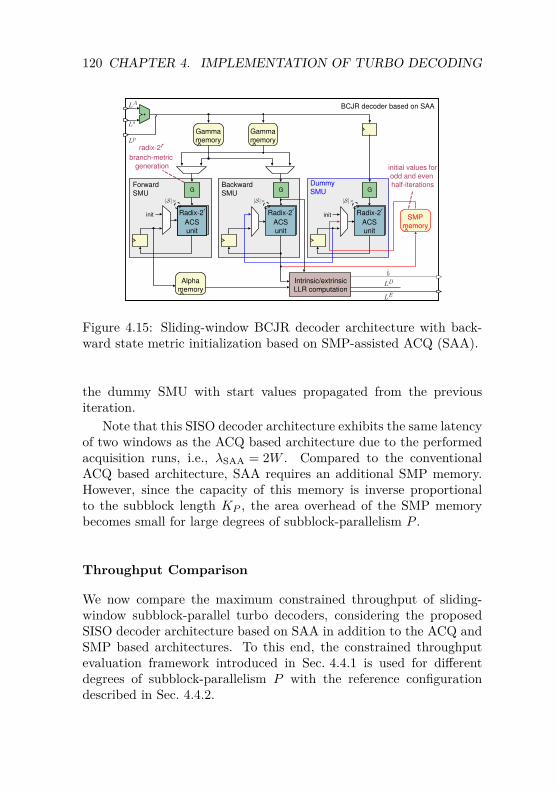
120 CHAPTER 4. IMPLEMENTATION OF TURBO DECODING
G
Intrinsic/extrinsic
LLR computation
Radix-2r
ACS
unit
init
Alpha
memory
Forward
SMU
BCJR decoder based on SAA
G G
Gamma
memory
Gamma
memory
Backward
SMU
Dummy
SMU
radix-2r
branch-metric
generation
Radix-2r
ACS
unit
Radix-2r
ACS
unit
SMP
memory
init
|S|× |S|× |S|×
initial values for
odd and even
half-iterations
LE
LD
b
Lp
Ls
LA
Figure 4.15: Sliding-window BCJR decoder architecture with back-ward state metric initialization based on SMP-assisted ACQ (SAA).
the dummy SMU with start values propagated from the previousiteration.
Note that this SISO decoder architecture exhibits the same latencyof two windows as the ACQ based architecture due to the performedacquisition runs, i.e., λSAA = 2W . Compared to the conventionalACQ based architecture, SAA requires an additional SMP memory.However, since the capacity of this memory is inverse proportionalto the subblock length KP , the area overhead of the SMP memorybecomes small for large degrees of subblock-parallelism P .
Throughput Comparison
We now compare the maximum constrained throughput of sliding-window subblock-parallel turbo decoders, considering the proposedSISO decoder architecture based on SAA in addition to the ACQ andSMP based architectures. To this end, the constrained throughputevaluation framework introduced in Sec. 4.4.1 is used for differentdegrees of subblock-parallelism P with the reference configurationdescribed in Sec. 4.4.2.
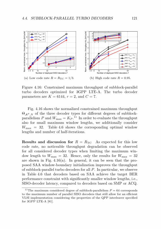
4.4. SUBBLOCK-PARALLEL TURBO DECODERS 121
2 4 8
0.5
1
1.5
SAA, Wmax
= 32
ACQ, Wmax
= 32
SMP, Wmax
= 32
4 8 16 32 64
Number of deployed SISO decoders P
1
2
3
4
5
6
7
No
rm.
co
nstr
ain
ed
ma
x.
thro
ug
hp
ut
ΘN
[b
it/c
ycle
]
2
(a) Low code rate R = RTC = 1/3.
2 4 8 16
1
2
3
SAA, Wmax
= KP
SAA, Wmax
= 32
ACQ, Wmax
= KP
SMP, Wmax
= KP
SMP, Wmax
= 32
2 4 8 16 32 64
Number of deployed SISO decoders P
1
2
3
4
5
6
7
No
rm.
co
nstr
ain
ed
ma
x.
thro
ug
hp
ut
ΘN
[b
it/c
ycle
]
(b) High code rate R = 0.95.
Figure 4.16: Constrained maximum throughput of subblock-parallelturbo decoders optimized for 3GPP LTE-A. The turbo decoderparameters are K = 6144, r = 2, and C = 7.
Fig. 4.16 shows the normalized constrained maximum throughputΘAP ,N of the three decoder types for different degrees of subblock-parallelism P and Wmax = KP .11 In order to evaluate the throughputalso for small maximum window lengths, we additionally considerWmax = 32. Table 4.6 shows the corresponding optimal windowlengths and number of half-iterations.
Results and discussion for R = RTC As expected for this lowcode rate, no noticeable throughput degradation can be observedfor all considered decoder types when limiting the maximum win-dow length to Wmax = 32. Hence, only the results for Wmax = 32are shown in Fig. 4.16(a). In general, it can be seen that the pro-posed SAA window-boundary initialization improves the throughputof subblock-parallel turbo decoders for all P . In particular, we observein Table 4.6 that decoders based on SAA achieve the target BERperformance constraint with significantly smaller window lengths, i.e.,SISO-decoder latency, compared to decoders based on SMP or ACQ.
11The maximum considered degree of subblock-parallelism P = 64 correspondsto the maximum number of parallel SISO decoders that still allow for an efficientVLSI implementation considering the properties of the QPP interleaver specifiedfor 3GPP LTE-A [81].
122 CHAPTER 4. IMPLEMENTATION OF TURBO DECODING
Thus, SAA is able to alleviate the parallel turbo-decoder predicamentto a great extent. For P = 64, for instance, SAA leads to a throughputgain of 20% compared to SMP. Compared to ACQ, the gain is largerthan 10%.
Results and discussion for R = 0.95 For high code rates (seeFig. 4.16(b)), all three decoder types unsurprisingly require largerwindow lengths to meet the performance target, and substantial degra-dation in throughput can be observed when limiting the maximumwindow length to Wmax = 32. The throughput degradation is es-pecially pronounced for smaller P . This observation indicates thatfor small P , the throughput is generally maximized by trading ahigh SISO-decoder latency for a small number of half-iterations, i.e.,the pairs (W ∗, I∗) lie in the lower right part of the trade-off curvesintroduced in Fig. 4.14(a). For large P on the other hand, it seemsmore important to reduce the SISO-decoder latency at the cost ofmore half-iterations.
Comparing the three decoder types, it can be observed that ACQis highly ill-suited for high code rate as the required window lengthsbecome impractically large. For P = 64 for instance, the minimumwindow length required to achieve the target performance is largerthan the subblock length KP , and thus, no valid (W, I) pairs can befound. For small maximum window length Wmax = 32, no valid pairsat all exist for this decoder type over all considered P . The other twodecoder architectures, on the other hand, achieve the performancetarget also for Wmax = 32. However, the proposed SAA leads tosubstantially higher throughput than SMP, mainly due to its fasterconvergence speed. For instance, at P = 64 and Wmax = 32, the SAAbased turbo decoder exhibits a throughput gain of 30% compared tothe decoder based on SMP.
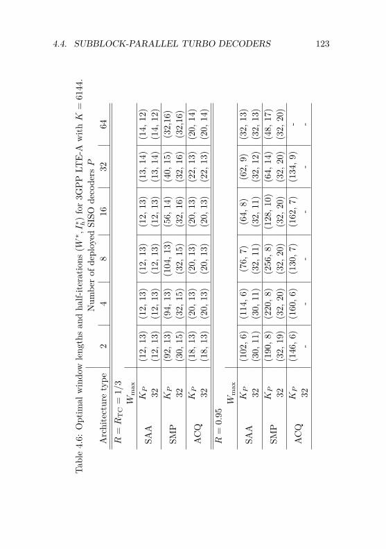
4.4. SUBBLOCK-PARALLEL TURBO DECODERS 123
Tabl
e4.
6:O
ptim
alw
indo
wle
ngth
san
dha
lf-ite
ratio
ns(W∗ ,I∗ h)
for
3GPP
LTE-
Aw
ithK
=61
44.
Num
ber
ofde
ploy
edSI
SOde
code
rsP
Arc
hite
ctur
ety
pe2
48
1632
64R
=R
TC
=1/
3W
max
SAA
KP
(12,
13)
(12,
13)
(12,
13)
(12,
13)
(13,
14)
(14,
12)
32(1
2,13
)(1
2,13
)(1
2,13
)(1
2,13
)(1
3,14
)(1
4,12
)
SMP
KP
(92,
13)
(94,
13)
(104
,13)
(56,
14)
(40,
15)
(32,
16)
32(3
0,15
)(3
2,15
)(3
2,15
)(3
2,16
)(3
2,16
)(3
2,16
)
AC
QKP
(18,
13)
(20,
13)
(20,
13)
(20,
13)
(22,
13)
(20,
14)
32(1
8,13
)(2
0,13
)(2
0,13
)(2
0,13
)(2
2,13
)(2
0,14
)R
=0.
95W
max
SAA
KP
(102
,6)
(114
,6)
(76,
7)(6
4,8)
(62,
9)(3
2,13
)32
(30,
11)
(30,
11)
(32,
11)
(32,
11)
(32,
12)
(32,
13)
SMP
KP
(190
,8)
(220
,8)
(256
,8)
(128
,10)
(64,
14)
(48,
17)
32(3
2,19
)(3
2,20
)(3
2,20
)(3
2,20
)(3
2,20
)(3
2,20
)
AC
QKP
(146
,6)
(160
,6)
(130
,7)
(162
,7)
(134
,9)
-32
--
--
--
124 CHAPTER 4. IMPLEMENTATION OF TURBO DECODING
4.4.4 VLSI Implementation Trade-off AnalysisIn what follows, the VLSI implementation complexity of sliding-windowsubblock-parallel turbo decoders is studied for different degrees ofsubblock-parallelism P . The analysis is based on synthesis resultsof the three discussed SISO decoder architectures in 65 nm CMOStechnology, taking into account the constrained throughput evaluationpresented in Sec. 4.4.3.
Preliminaries
All three SISO decoder architectures have been optimized for radix-4, i.e., r = 2, trellis processing and fully support the 3GPP LTEand LTE-A standards with Kmax = 6144. To achieve near-optimalerror-rate performance, the systematic and parity input LLRs arequantized to 5 bit, the extrinsic LLRs to 6 bit, and the state metricsto 10 bit. Furthermore, the SMP memories have been implementedas SRAM macrocells, whereas the Gamma and Alpha memories havebeen implemented using latch-based SCMs in order to simplify thegeneric synthesis study.
Throughput versus Silicon Area
Fig. 4.17 shows the trade-off between constrained maximum turbodecoder throughput Θ (in ns/bit) and total SISO decoder siliconarea A (in mm2). Note that the considered area only contains theshare of the P SISO decoders, neglecting the other components ofthe turbo decoder, such as the input and intermediate memories oraddress generation circuits. We emphasize, however, that the SISOdecoders dominate the overall turbo decoder area for P ≥ 8 [80].We consider operation at high code rate R = 0.95, which is thecorner where subblock-parallel turbo decoders are especially affectedby the parallel turbo-decoder predicament. For each implementationin Fig. 4.17, the corresponding optimal window lengths and numberof half-iterations shown in Table 4.6 have been used to determine theexact memory capacities and the constrained maximum throughput.All SISO decoders have been synthesized at maximum clock frequency800 MHz.
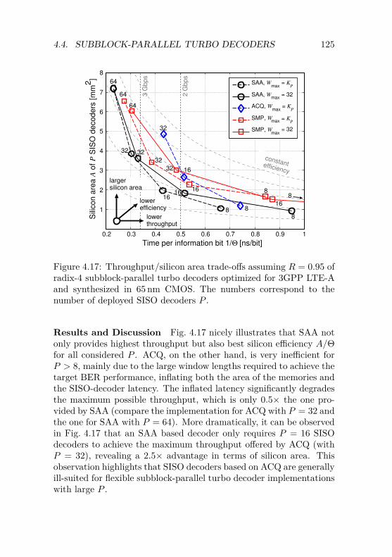
4.4. SUBBLOCK-PARALLEL TURBO DECODERS 125
0.2 0.3 0.4 0.5 0.6 0.7 0.8 0.9 1
1
2
3
4
5
6
7
8
Time per information bit 1/Θ [ns/bit]
Sili
co
n a
rea
A o
f P
SIS
O d
eco
de
rs [
mm
2]
SAA, Wmax
= KP
SAA, Wmax
= 32
ACQ, Wmax
= KP
SMP, Wmax
= 32SMP, Wmax
= KP
32
64
64
64
32
32
16
32 32
16
16
8 8
8
16
8
constantefficiency
larger silicon area
2 G
bp
s
8
lowerthroughput
lowerefficiency
3 G
bp
s
16
Figure 4.17: Throughput/silicon area trade-offs assuming R = 0.95 ofradix-4 subblock-parallel turbo decoders optimized for 3GPP LTE-Aand synthesized in 65 nm CMOS. The numbers correspond to thenumber of deployed SISO decoders P .
Results and Discussion Fig. 4.17 nicely illustrates that SAA notonly provides highest throughput but also best silicon efficiency A/Θfor all considered P . ACQ, on the other hand, is very inefficient forP > 8, mainly due to the large window lengths required to achieve thetarget BER performance, inflating both the area of the memories andthe SISO-decoder latency. The inflated latency significantly degradesthe maximum possible throughput, which is only 0.5× the one pro-vided by SAA (compare the implementation for ACQ with P = 32 andthe one for SAA with P = 64). More dramatically, it can be observedin Fig. 4.17 that an SAA based decoder only requires P = 16 SISOdecoders to achieve the maximum throughput offered by ACQ (withP = 32), revealing a 2.5× advantage in terms of silicon area. Thisobservation highlights that SISO decoders based on ACQ are generallyill-suited for flexible subblock-parallel turbo decoder implementationswith large P .
126 CHAPTER 4. IMPLEMENTATION OF TURBO DECODING
Decoders based on SMP become more efficient than ACQ baseddecoders for P ≥ 16, mainly due to the smaller window lengthsthat can be used to achieve the target BER performance constraint.However, SMP is considerably outperformed by SAA in terms ofthroughput and silicon efficiency for all P . Interestingly, we find thatP = 16 and P = 32 SAA based turbo decoders reach approximatelythe same throughput as P = 32 and P = 64 SMP based decoders,respectively. The area advantage of SAA in these cases amounts to1.7×.
Finally, observe that allowing for Wmax = KP in general leads tolarger silicon area, but also to better silicon efficiency than constrain-ing Wmax to smaller window lengths.
In summary, the above discussion enables one to conclude thatthe presented SAA based SISO decoder architecture is most suited forflexible subblock-parallel turbo decoders since it leads to significantlyhigher throughput and better silicon efficiency than the prior-art so-lutions.
Proof-of-Concept Implementation
As a proof-of-concept, a P = 16, W = 30 subblock-parallel turbodecoder based on the presented SISO decoder architecture with SAAwindow-boundary initialization has been implemented and manufac-tured in 65 nm CMOS.12 The large input and intermediate memorieshave been implemented with SRAM macrocells. The implementationof the (de-)interleaving networks is based on the efficient and flexiblemaster-slave batcher network introduced in [80].
Table 4.7 summarizes the measured key characteristics of the ASICprototype and provides comparison with prior-art implementations.The decoder is the first fabricated and measured turbo decoder im-plementation that achieves a throughput in excess of 1 Gbps. TheASIC uses 201 kbit of SRAM and occupies an active cell area of2.02 mm2 (including the SRAM macrocells), where the share of theSISO decoders amounts to 80%. Due to the use of the describedSAA based SISO decoder architecture, the high throughput can besustained over the full range of code rates, without any concession
12The ASIC integration has been carried out by another PhD student at thesame research institute. Refer to [26] for more information on the fabricated ASIC.
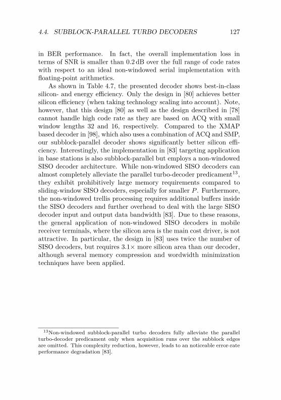
4.4. SUBBLOCK-PARALLEL TURBO DECODERS 127
in BER performance. In fact, the overall implementation loss interms of SNR is smaller than 0.2 dB over the full range of code rateswith respect to an ideal non-windowed serial implementation withfloating-point arithmetics.
As shown in Table 4.7, the presented decoder shows best-in-classsilicon- and energy efficiency. Only the design in [80] achieves bettersilicon efficiency (when taking technology scaling into account). Note,however, that this design [80] as well as the design described in [78]cannot handle high code rate as they are based on ACQ with smallwindow lengths 32 and 16, respectively. Compared to the XMAPbased decoder in [98], which also uses a combination of ACQ and SMP,our subblock-parallel decoder shows significantly better silicon effi-ciency. Interestingly, the implementation in [83] targeting applicationin base stations is also subblock-parallel but employs a non-windowedSISO decoder architecture. While non-windowed SISO decoders canalmost completely alleviate the parallel turbo-decoder predicament13,they exhibit prohibitively large memory requirements compared tosliding-window SISO decoders, especially for smaller P . Furthermore,the non-windowed trellis processing requires additional buffers insidethe SISO decoders and further overhead to deal with the large SISOdecoder input and output data bandwidth [83]. Due to these reasons,the general application of non-windowed SISO decoders in mobilereceiver terminals, where the silicon area is the main cost driver, is notattractive. In particular, the design in [83] uses twice the number ofSISO decoders, but requires 3.1× more silicon area than our decoder,although several memory compression and wordwidth minimizationtechniques have been applied.
13Non-windowed subblock-parallel turbo decoders fully alleviate the parallelturbo-decoder predicament only when acquisition runs over the subblock edgesare omitted. This complexity reduction, however, leads to an noticeable error-rateperformance degradation [83].
128 CHAPTER 4. IMPLEMENTATION OF TURBO DECODING
Table4.7:
Com
parisonofparallelturbo
decoderim
plementations
forLT
E/LTE-A
.T
hisw
orka
[78][80]
[81][98]
[83]A
rchitecturetype
Psliding-w
indowBC
JRX
MA
PP
NSW
-BCJR
Radix/Parallelism
4/162/8
4/82/64
2/84/32
Supportfor
highR
√×
×√
√√
Technology[nm
]65
90130
6565
65N
om.
supplyV
DD
[V]
1.21.0
1.20.9
1.11.1
Implem
ent.status
siliconpost-layout
Core
area[m
m2]
2.492.10
3.578.3
2.17.7
Max.
clockfrequency
410b
275302
400300
450in
[MH
z]M
ax.throughput c
1013189
3911400
1772346
in[M
bps]Silicon
efficiency
2.4611.11
9.135.93
11.863.28
in[m
m2
ns/bit](4.19
d)(1.14
d)Energy
efficiency
0.170.21
0.370.11
0.31n.a.
in[nJ/bit/iter]
(0.22d)
(0.19d)
(0.20d)
(0.37d)
aThe
chipintegration
was
carriedout
byanother
PhD
studentat
thesam
eresearch
institute[26].
bMeasured
clockfrequency
shows
largedeviation
(-35%)
fromclock
frequencyextracted
frompost-layout
data.cA
tI
h=
11half-iterations.
dTechnologyscaling
to65
nm,V
DD
=1.2V
accordingto
[19]:tp
d∼
1/s,A∼
1/s 2,
Pdyn∼
1/s·(V′D
D/V
DD
) 2.
Chapter 5
Channel DecodingChain Design for UMTS
In the previous chapters the channel decoders were considered asstand-alone blocks. In practical digital baseband receivers, however,the described channel decoders are typically embedded in sophis-ticated channel decoding chains that provide additional importantfeatures to further increase the reliability of transmission. Such chan-nel decoding chains must preferably be implemented as application-specific VLSI circuits along with the other components of the digitalbaseband receiver in order to profit from the cost and power advantageof systems implemented in fully dedicated hardware over software-programmable solutions. The main VLSI implementation challengeconcerning channel decoding chains in wireless systems (beside thepreviously discussed channel decoders) arises from the large numberof operation modes that must be supported. The need for such highflexibility requires that the architecture is designed for the worst-case operation mode (i.e., the mode that requires most hardwareresources), while the power consumption remains as low as possiblefor the less complex modes of the considered standard.
This chapter outlines the design and VLSI implementation of thecomplete channel decoding chain for the TD-HSPA+ LCR standard,which is representative for typical channel decoding chains in current
129
130 CHAPTER 5. CHANNEL DECODING CHAIN FOR UMTS
and emerging cellular standards. The chain has been integrated aspart of a digital downlink baseband receiver ASIC. In Sec. 5.1 weprovide an overview on the structure of the considered 3G cellularstandard and then present in Sec. 5.2 the proposed baseband receiverVLSI architecture with a particular focus on the channel decodingchain. The ASIC implementation results are provided in Sec. 5.3.
5.1 Overview on TD-SCDMA EvolutionsTD-HSPA+ low chip rate (LCR) is the latest enhancement of thetime-division synchronous code-division multiple access (TD-SCDMA)standard, the narrow-band option of the time division duplex (TDD)variant of 3GPP UMTS. Due to its TDD property (as opposed tothe frequency division duplex variant WCDMA commonly used inEurope) TD-SCDMA has received an increasing attention, partiallybecause it allows for a dynamic resource allocation for uplink anddownlink according to current traffic needs, which helps to cope withasymmetric traffic highly efficiently, and partially because no costlyduplexers are required in related radio transceiver realizations.
The multiple access technology of TD-SCDMA is a combination oftime-division multiple access (TDMA) and direct-spread code-divisionmultiple access (CDMA). As illustrated in Fig. 5.1, the physical chan-nel resources are structured into radio frames, subframes and times-lots [99]. Each frame of 10 ms duration comprises two subframes of5 ms, and each subframe consists of seven timeslots. The timeslotsare further divided into two data fields, a specific midamble sequence,and a guard period. The number of chips per timeslot is 864 and thechip duration is 781.25 ns (according to a chip rate of 1.28 Mcps). Inthe data fields of the individual timeslots, up to 16 users can transmitsimultaneously using CDMA with spreading factors of 1, 4, 8 or1
16. A flexible resource allocation is achieved by the possibility toassign multiple CDMA codes to a single user. The assignments ofthe timeslots within a subframe to downlink and uplink is specifiedusing two switching points. The first timeslot is always assigned to
1In the downlink only the spreading factors 1 or 16 are used, whereas in theuplink the use of all four spreading factors is possible.
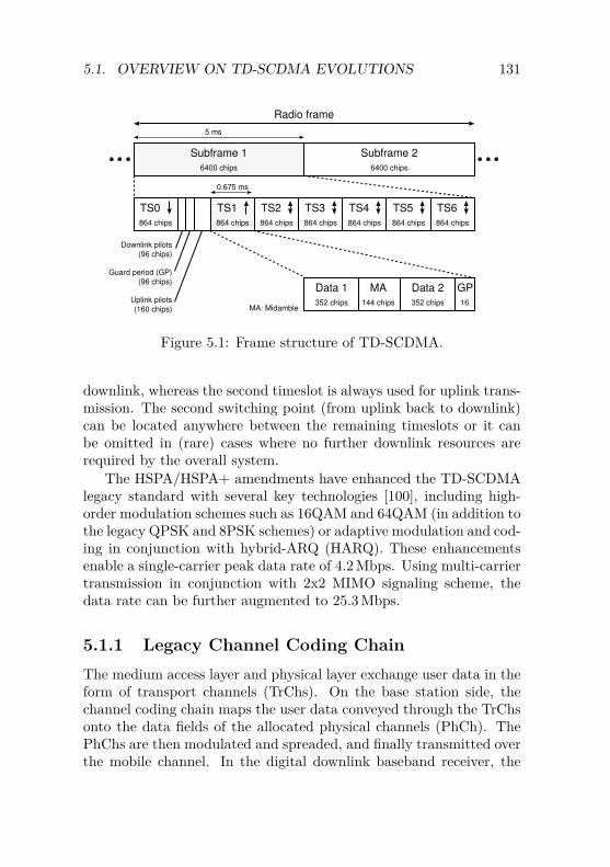
5.1. OVERVIEW ON TD-SCDMA EVOLUTIONS 131
864 chips
TS0
864 chips
TS1
864 chips
TS2
864 chips
TS3
864 chips
TS4
864 chips
TS5
864 chips
TS6
Subframe 1
6400 chips
Subframe 2
6400 chips
5 ms
0.675 ms
Data 1 MA Data 2 GP
352 chips 144 chips 352 chips 16
Downlink pilots
(96 chips)
Guard period (GP)
(96 chips)
Uplink pilots
(160 chips)
Radio frame
MA: Midamble
Figure 5.1: Frame structure of TD-SCDMA.
downlink, whereas the second timeslot is always used for uplink trans-mission. The second switching point (from uplink back to downlink)can be located anywhere between the remaining timeslots or it canbe omitted in (rare) cases where no further downlink resources arerequired by the overall system.
The HSPA/HSPA+ amendments have enhanced the TD-SCDMAlegacy standard with several key technologies [100], including high-order modulation schemes such as 16QAM and 64QAM (in addition tothe legacy QPSK and 8PSK schemes) or adaptive modulation and cod-ing in conjunction with hybrid-ARQ (HARQ). These enhancementsenable a single-carrier peak data rate of 4.2 Mbps. Using multi-carriertransmission in conjunction with 2x2 MIMO signaling scheme, thedata rate can be further augmented to 25.3 Mbps.
5.1.1 Legacy Channel Coding ChainThe medium access layer and physical layer exchange user data in theform of transport channels (TrChs). On the base station side, thechannel coding chain maps the user data conveyed through the TrChsonto the data fields of the allocated physical channels (PhCh). ThePhChs are then modulated and spreaded, and finally transmitted overthe mobile channel. In the digital downlink baseband receiver, the
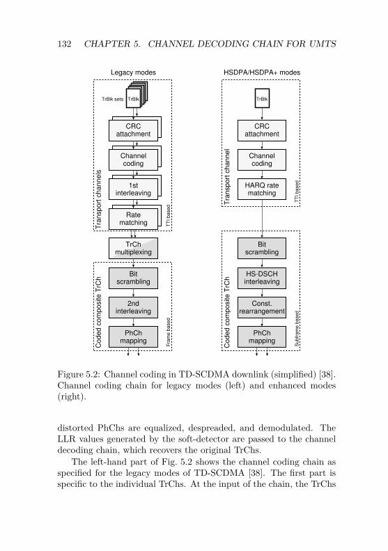
132 CHAPTER 5. CHANNEL DECODING CHAIN FOR UMTS
CRCattachment
Channelcoding
1stinterleaving
Ratematching
CRCattachment
Channelcoding
1stinterleaving
Ratematching
Bitscrambling
2ndinterleaving
PhChmapping
TrBlkT
ran
sp
ort
ch
an
ne
lsC
od
ed
co
mp
osite
TrC
h
TrChmultiplexing
CRCattachment
Channelcoding
TrBlk
Bitscrambling
HS-DSCHinterleaving
Const.rearrangement
PhChmapping
HARQ ratematching
Co
de
d c
om
po
site
TrC
hT
ran
sp
ort
ch
an
ne
l
Legacy modes HSDPA/HSDPA+ modes
TrBlk sets
TT
I b
ase
dF
ram
e b
ase
d
TT
I b
ase
dS
ub
fra
me
ba
se
d
Figure 5.2: Channel coding in TD-SCDMA downlink (simplified) [38].Channel coding chain for legacy modes (left) and enhanced modes(right).
distorted PhChs are equalized, despreaded, and demodulated. TheLLR values generated by the soft-detector are passed to the channeldecoding chain, which recovers the original TrChs.
The left-hand part of Fig. 5.2 shows the channel coding chain asspecified for the legacy modes of TD-SCDMA [38]. The first part isspecific to the individual TrChs. At the input of the chain, the TrChs
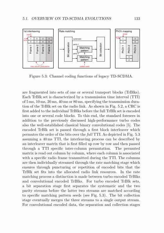
5.1. OVERVIEW ON TD-SCDMA EVOLUTIONS 133
Fra
me 1
Fra
me 3
Fra
me 2
Fra
me 4
read
inter-column permutation
PhC
h 1
PhC
h 2
PhC
h 3
write
Bit s
epara
tion
Bit c
olle
ction
Matchingpattern
Matchingpattern
pattern seed
systematic
parity-1
parity-2
1st interleaving Rate matching PhCh mappingread
write1 3 2 4
5 7 6 8
1 3
4 6
5
2
Figure 5.3: Channel coding functions of legacy TD-SCDMA.
are fragmented into sets of one or several transport blocks (TrBlks).Each TrBlk set is characterized by a transmission time interval (TTI)of 5 ms, 10 ms, 20 ms, 40 ms or 80 ms, specifying the transmission dura-tion of the TrBlk set on the radio link. As shown in Fig. 5.2, a CRC isfirst added to the individual TrBlks before the full TrBlk set is encodedinto one or several code blocks. To this end, the standard foresees inaddition to the previously discussed high-performance turbo codesalso the well-established classical binary convolutional codes [5]. Theencoded TrBlk set is passed through a first block interleaver whichpermutes the order of the bits over the full TTI. As depicted in Fig. 5.3assuming a 40 ms TTI, the interleaving process can be described byan interleaver matrix that is first filled up row by row and then passedthrough a TTI specific inter-column permutation. The permutedmatrix is read out column by column, where each column is associatedwith a specific radio frame transmitted during the TTI. The columnsare then individually streamed through the rate matching stage whichensures through puncturing or repetition of encoded bits that theTrBlk set fits into the allocated radio link resources. In the ratematching process a distinction is made between turbo encoded TrBlksand convolutional encoded TrBlks. For turbo encoded TrBlk sets,a bit separation stage first separates the systematic and the twoparity streams before the latter two streams are matched accordingto specific matching pattern seeds (see Fig. 5.3). The bit collectionstage eventually merges the three streams to a single output stream.For convolutional encoded data, the separation and collection stages
134 CHAPTER 5. CHANNEL DECODING CHAIN FOR UMTS
are transparent and rate matching is performed over the full singlestream. Observe from Fig. 5.2 that multiple TrChs per TTI can beactive concurrently. These TrChs must be processed separately beforethey are multiplexed into a single so-called coded composite transportchannel (CCTrCh).
The second part of the chain is specific to the multiplexed TrChsand processes the CCTrCh on a radio frame basis (or subframe basisfor 5 ms TTIs). The individual frames are scrambled with a pseudo-random sequence and then passed to a second interleaver stage whichpermutes the order of the bits either over the full radio frame orwithin each timeslot of the frame separately. Similar to the firstinterleaver, this second interleaver is also a block interleaver withinter-column permutations, but the related matrix contains a fixednumber of columns. Finally, the bits are mapped onto the physicalchannel resources, i.e., the timeslots and CDMA codes. This PhChmapping is performed individually for the two subframes and for eachallocated timeslot within the subframes. In particular, as illustratedin Fig. 5.3, the bitstream is written into a matrix row-wise wherethe odd-numbered columns are filled in forward order and the even-numbered columns in reversed order. The filled columns (which canhave a varying number of rows) of this matrix are read out in for-ward order and are associated with the PhChs, i.e. the CDMA codes,transmitted in the respective timeslot and subframe. After the PhChmapping, an encoded transport format combination indicator (TFCI)is included into the data fields of the transmitted timeslots, whichsignals the receiver how to decode the conveyed TrChs. The TFCIsare encoded using a masked first-order Reed-Muller code [38].
5.1.2 Enhanced Channel Coding ChainThe right-hand part of Fig. 5.2 shows the channel coding chain asspecified for the high-speed downlink shared channel (HS-DSCH) —the data TrCh type that was added to the legacy types to carry theenhanced HSDPA/HSDPA+ modes. Note that this chain must besupported in addition to the legacy chain in TD-HSPA+ compliantdownlink baseband receivers. Compared to the legacy chain, the en-hanced chain exhibits a reduced worst-case latency, partially becauseit only allows for a single active TrCh with a 5 ms TTI and partially
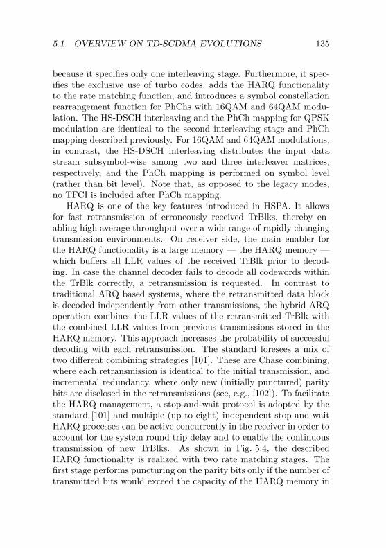
5.1. OVERVIEW ON TD-SCDMA EVOLUTIONS 135
because it specifies only one interleaving stage. Furthermore, it spec-ifies the exclusive use of turbo codes, adds the HARQ functionalityto the rate matching function, and introduces a symbol constellationrearrangement function for PhChs with 16QAM and 64QAM modu-lation. The HS-DSCH interleaving and the PhCh mapping for QPSKmodulation are identical to the second interleaving stage and PhChmapping described previously. For 16QAM and 64QAM modulations,in contrast, the HS-DSCH interleaving distributes the input datastream subsymbol-wise among two and three interleaver matrices,respectively, and the PhCh mapping is performed on symbol level(rather than bit level). Note that, as opposed to the legacy modes,no TFCI is included after PhCh mapping.
HARQ is one of the key features introduced in HSPA. It allowsfor fast retransmission of erroneously received TrBlks, thereby en-abling high average throughput over a wide range of rapidly changingtransmission environments. On receiver side, the main enabler forthe HARQ functionality is a large memory — the HARQ memory —which buffers all LLR values of the received TrBlk prior to decod-ing. In case the channel decoder fails to decode all codewords withinthe TrBlk correctly, a retransmission is requested. In contrast totraditional ARQ based systems, where the retransmitted data blockis decoded independently from other transmissions, the hybrid-ARQoperation combines the LLR values of the retransmitted TrBlk withthe combined LLR values from previous transmissions stored in theHARQ memory. This approach increases the probability of successfuldecoding with each retransmission. The standard foresees a mix oftwo different combining strategies [101]. These are Chase combining,where each retransmission is identical to the initial transmission, andincremental redundancy, where only new (initially punctured) paritybits are disclosed in the retransmissions (see, e.g., [102]). To facilitatethe HARQ management, a stop-and-wait protocol is adopted by thestandard [101] and multiple (up to eight) independent stop-and-waitHARQ processes can be active concurrently in the receiver in order toaccount for the system round trip delay and to enable the continuoustransmission of new TrBlks. As shown in Fig. 5.4, the describedHARQ functionality is realized with two rate matching stages. Thefirst stage performs puncturing on the parity bits only if the number oftransmitted bits would exceed the capacity of the HARQ memory in
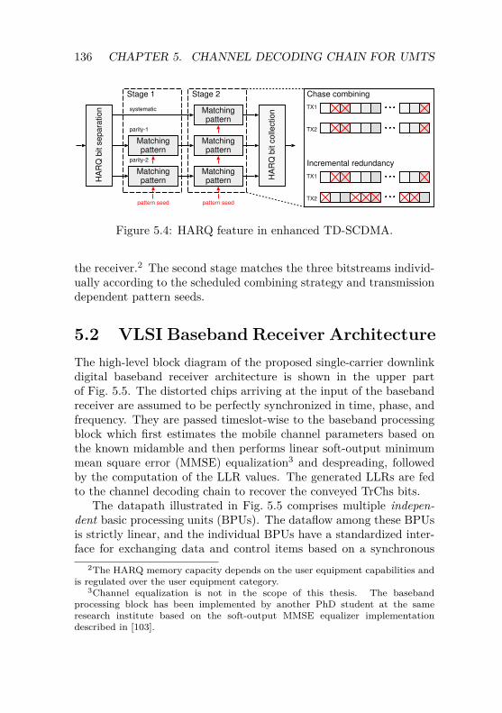
136 CHAPTER 5. CHANNEL DECODING CHAIN FOR UMTS
HA
RQ
bit s
ep
ara
tio
n
HA
RQ
bit c
olle
ctio
n
Matchingpattern
Matchingpattern
pattern seed
systematic
parity-1
parity-2
Matchingpattern
Matchingpattern
pattern seed
Matchingpattern
Stage 1 Stage 2 Chase combining
Incremental redundancy
TX1
TX2
TX1
TX2
Figure 5.4: HARQ feature in enhanced TD-SCDMA.
the receiver.2 The second stage matches the three bitstreams individ-ually according to the scheduled combining strategy and transmissiondependent pattern seeds.
5.2 VLSI Baseband Receiver ArchitectureThe high-level block diagram of the proposed single-carrier downlinkdigital baseband receiver architecture is shown in the upper partof Fig. 5.5. The distorted chips arriving at the input of the basebandreceiver are assumed to be perfectly synchronized in time, phase, andfrequency. They are passed timeslot-wise to the baseband processingblock which first estimates the mobile channel parameters based onthe known midamble and then performs linear soft-output minimummean square error (MMSE) equalization3 and despreading, followedby the computation of the LLR values. The generated LLRs are fedto the channel decoding chain to recover the conveyed TrChs bits.
The datapath illustrated in Fig. 5.5 comprises multiple indepen-dent basic processing units (BPUs). The dataflow among these BPUsis strictly linear, and the individual BPUs have a standardized inter-face for exchanging data and control items based on a synchronous
2The HARQ memory capacity depends on the user equipment capabilities andis regulated over the user equipment category.
3Channel equalization is not in the scope of this thesis. The basebandprocessing block has been implemented by another PhD student at the sameresearch institute based on the soft-output MMSE equalizer implementationdescribed in [103].
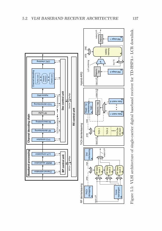
5.2. VLSI BASEBAND RECEIVER ARCHITECTURE 137
Channel estimation
LLR computation
Baseb
an
d p
rocessin
g
TFCI extraction
RF deinterleaving
Bit descrambling
CRC checking
Ch
an
nel d
eco
din
g c
hain
Tu
rbo
co
re
Vite
rbi co
re
Ch
an
ne
l d
eco
din
g
BP
co
ntr
ol u
nit
Dec c
on
tro
l u
nit
MMSE equalization
RF buffer
Hybrid-ARQ
TrCh deinterelaving
RX
co
ntr
ol u
nit
RF
De
int
me
m 1
Ph
Ch
de
ma
pp
ing
2n
d
inte
rle
avin
g
Co
nst.
rea
rra
ng
em
.
inp
ut
LL
R
ou
tpu
t L
LR
TrC
h D
e-
int
me
m
TrC
h 1
TrC
h 2
Rate match 1
Rate match 8
inp
ut
LL
R
Re
ad
/ 1
st
inte
rle
avin
g
log
ic
write
rea
d
De
pu
nc /
re
po
utp
ut
LL
R
rea
dw
rite
inp
ut
LL
R
rea
dw
rite H
AR
Q
me
mo
ry
RM stage 2
RM stage 1
De
pu
nc
De
pu
nc /
rep
ou
tpu
t L
LR
LL
R c
om
bin
ing
RF
dein
terleavin
gT
rCh d
ein
terleavin
gH
ybrid-A
RQ
De
cR
pt
De
cC
trl
BP
Rp
tB
PC
trl
firs
t T
X
0
TrC
h p
roce
ssin
gC
CT
rCh
pro
ce
ssin
g
Sh
are
d
me
mo
ry
RF
De
int
me
m 2
RF
De
int
me
m 3
Figu
re5.
5:V
LSIa
rchi
tect
ure
ofsin
gle-
carr
ier
digi
talb
aseb
and
rece
iver
for
TD
-HSP
A+
LCR
dow
nlin
k.
138 CHAPTER 5. CHANNEL DECODING CHAIN FOR UMTS
handshake protocol. Each BPU operates on chunks of data of awell-defined scope (e.g., a timeslot, a subframe, a radio frame or TTI),and every new data chunk is initiated by a control item received fromthe associated control unit, providing the BPU with the necessaryinformation to process the data chunk. Once the current data chunkhas been processed, a report is issued to the control unit, which inturn must acknowledge this report before a new data chunk can beprocessed. This approach enables a simple self-synchronization of thedatapath, irrespective of the latency of the individual BPUs.
In general, a substantial amount of memory is required for buffer-ing and realizing the HARQ functionality and the two deinterleavingstages. We emphasize that all these memories are realized as dedicatedon-chip SRAMs, which enables a true single-chip baseband solutionand which avoids the significant overhead in terms of silicon area,power, and latency of centralized memory architectures or off-chipsolutions that are typically employed in software-programmable base-band architectures.
5.2.1 Channel Decoding Chain ArchitectureThe main VLSI implementation challenge of the channel decodingchain (beside the turbo decoder discussed in Chapter 4) arises fromthe countless operation modes that must be supported. In particular,the architecture has to support both chains shown in Fig. 5.2 and allblocks in these two chains are affected by the characteristics of thecurrently processed TrChs (such as the finely granulated TrBlk size,TTI, coding or rate matching seeds) and the allocated PhCh resourcesin terms of CDMA codes and timeslots. These parameters can betuned by the higher layers on a TTI basis. It is important to notethat the utilization of the channel decoding chain for the differentpossible modes varies to an extreme extent. For instance, only 88LLR values enter the chain per subframe when one timeslot and oneCDMA code with QPSK are assigned. With five assigned timeslotsand 16 CDMA codes using 64QAM modulation, the number of LLRvalues that must be processed per subframe increases by two ordersof magnitude to 21120. To arrive at an efficient VLSI architectureunder these stringent flexibility requirements, a significant effort hasbeen put into identifying the commonalities shared by the two chains
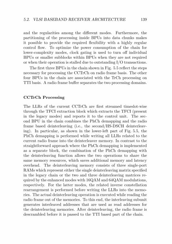
5.2. VLSI BASEBAND RECEIVER ARCHITECTURE 139
and the regularities among the different modes. Furthermore, thepartitioning of the processing inside BPUs into data chunks makesit possible to provide the required flexibility with a highly regularcontrol flow. To optimize the power consumption of the chain forlower-complexity modes, clock gating is used to turn off individualBPUs or smaller subblocks within BPUs when they are not requiredor when their operation is stalled due to outstanding I/O transactions.
The first three BPUs in the chain shown in Fig. 5.5 reflect the stepsnecessary for processing the CCTrCh on radio frame basis. The otherfour BPUs in the chain are associated with the TrCh processing onTTI basis. A radio frame buffer separates the two processing domains.
CCTrCh Processing
The LLRs of the current CCTrCh are first streamed timeslot-wisethrough the TFCI extraction block which extracts the TFCI (presentin the legacy modes) and reports it to the control unit. The sec-ond BPU in the chain combines the PhCh demapping and the radioframe based deinterleaving (i.e., the second/HS-DSCH deinterleav-ing). In particular, as shown in the lower-left part of Fig. 5.5, thePhCh demapping is performed while writing all LLRs related to thecurrent radio frame into the deinterleaver memory. In contrast to thestraightforward approach where the PhCh demapping is implementedas a separate block, the combination of the PhCh demapping withthe deinterleaving function allows the two operations to share thesame memory resources, which saves additional memory and latencyoverhead. The deinterleaving memory consists of three single-portRAMs which represent either the single deinterleaving matrix specifiedin the legacy chain or the two and three deinterleaving matrices re-quired by the enhanced modes with 16QAM and 64QAM modulations,respectively. For the latter modes, the related inverse constellationrearrangement is performed before writing the LLRs into the memo-ries. The actual deinterleaving operation is executed while reading theradio frame out of the memories. To this end, the interleaving subunitgenerates interleaved addresses that are used as read addresses forthe deinterleaving memories. After deinterleaving, the radio frame isdescrambled before it is passed to the TTI based part of the chain.
140 CHAPTER 5. CHANNEL DECODING CHAIN FOR UMTS
TrCh Processing
The first BPU in the TTI based part of the channel decoding chainperforms the TrCh deinterleaving (i.e., the first deinterleaving stage)and the rate dematching for the legacy modes of the standard. En-hanced TrChs of type HS-DSCH, on the other hand, are directlyforwarded to the subsequent BPU. As shown in the lower-middlepart of Fig. 5.5, all LLRs of the current TTI are first written intothe large single-port deinterleaver memory. Demultiplexing of themerged TrChs is performed while writing the LLRs into the memory.We emphasize that rate dematching is executed at the output sideof the memory, rather than at its input side as implied by the dataflow illustrated in the left-hand part of Fig. 5.2. This optimizationenables one to reduce the capacity of the deinterleaving memory bytwo thirds. In order to perform the rate dematching while reading outthe individual TrChs, up to eight (according to the maximum numberof eight columns in the associated interleaving matrix) separate ratematching units are instantiated. Each rate matching unit is associ-ated with a specific deinterleaved column of the interleaving matrixand incrementally discloses the corresponding rate matching pattern,taking into account the specified bit separation and bit collectionprocedure (see Fig. 5.3).
The subsequent Hybrid-ARQ BPU executes the rate dematch-ing and the described HARQ combining operation for the enhancedTrChs, whereas the legacy TrChs are directly forwarded to the output.As illustrated in the lower-right part of Fig. 5.5, the input LLR streamis dematched in accordance with the second-stage rate matching pro-cedure described in Fig. 5.4, combined with the stored combined LLRsfrom previous transmissions, and stored in the single-port HARQmemory. In the second step, the first-stage rate dematching is per-formed while reading the combined LLRs out of the memory.
The dematched LLRs are loaded codeword-wise into the inputbuffer of the channel decoding BPU and then decoded. Finally, thelast BPU in the channel decoding chain checks the CRC of the indi-vidual TrBlks and reports the corresponding results along with otherinformation extracted from the decoded bitstream to the control unit.
5.2. VLSI BASEBAND RECEIVER ARCHITECTURE 141
Control Unit
The control unit orchestrates the operation of the individual BPUs,taking into account the control items issued by the top-level receivercontrol unit as well as the information extracted from the reportsduring operation. In order to compile the control items for the TrChbased BPUs, the control unit must in every TTI first decode theextracted TFCI (for legacy modes) and then, based on the high-level information carried in the decoded TFCI or received from thereceiver control unit, compute a large set of additional variable TrChparameters, such as, e.g., the rate matching pattern seeds, the numberof codewords or the codeblock lengths. These parameters have ingeneral a large range of values (i.e., a large wordwidth) and therelated computations foresee an excessive use of multiplications anddivisions, which makes an efficient dedicated VLSI implementationrather challenging. To compute these TrCh parameters with smallarea overhead, a simple processor-like architecture has been designed.The processor comprises data registers and an optimized fixed-pointarithmetic logic unit consisting of a subtractor/adder, a pipelinedmultiplier, and a pipelined divider that are accessed according to asmall program realized as hardwired finite state machine (FSM). Theworst-case latency4 of the TrCh parameters computation togetherwith the TFCI decoding amounts to only 4000 + 550 clock cycles,which corresponds to only one twelfth of a timeslot duration whena minimum operating clock frequency of 85 MHz is considered. Toachieve best-possible hardware utilization of the channel decodingchain during operation, the control flow within the control unit ispipelined, enabling upstream BPUs to process new TTIs while down-stream BPUs are still processing older ones.
5.2.2 Complete Channel Decoding SolutionIn order to decode the specified binary (nconv, 1) convolutional codes,a dedicated Viterbi decoder [6] is required in addition to the turbodecoder discussed in Chapter 4. Although the VLSI implementationof Viterbi decoders is a well-studied subject in general, the various
4The considered worst-case scenario is a legacy setup with 80 ms TTI and fourmultiplexed TrChs in combination with a 48 bit TFCI codeword.
142 CHAPTER 5. CHANNEL DECODING CHAIN FOR UMTS
operation modes of the standard pose a significant implementationchallenge. This observation is valid for the considered standard in par-ticular, but also in general for recent and emerging cellular standards,where binary (nconv, 1) convolutional codes are still an importantingredient of the channel coding strategy, especially for control orlower-throughput data modes. In these standards, a single Viterbidecoder must typically support not only different block lengths andpunctured code rates, but also different constraint lengths (i.e., trellisstates) and generator polynomials (i.e., characteristics of the statetransitions). Furthermore, the constraint lengths found in these stan-dards can be as high as ν = 9 (corresponding to |S| = 2ν−1 = 256trellis states), which requires a careful area/throughput trade-off inrelated implementations to avoid an excessive area overhead.
Flexible Viterbi Decoder Architecture
The upper part of Fig. 5.6 shows the high-level block diagram ofour flexible radix-2 Viterbi decoder architecture. To account for thepossibly large constraint lengths, we consider here the area-economicmemory based trace-back (TB) method [93] to obtain the ML pathin a sliding-window fashion, rather than the RE method used in ourSOVA decoder architecture presented in Chapter 4.
Sequential forward recursion To provide the required flexibilityfor different constraint lengths and to enable a trade-off between areaand throughput, the architecture follows a sequential processing ap-proach where the characteristic |S| ACS computations associated witheach trellis step are performed sequentially in NACS clock cycles usinga set of PACS < |S| time-shared ACS units (i.e., NACS = |S|/PACS).Multiplexing and demultiplexing networks are required as consequenceof the sequential processing approach to route in every clock cyclethe proper set of PACS state metrics to the ACS units and write theupdated metrics back to the state metric register. To keep the com-plexity of these networks as low as possible, we exploit the inherentbutterfly structure in the trellis of convolutional codes and organizethe ACS units in PACS/2 pairs where each pair represents a radix-2
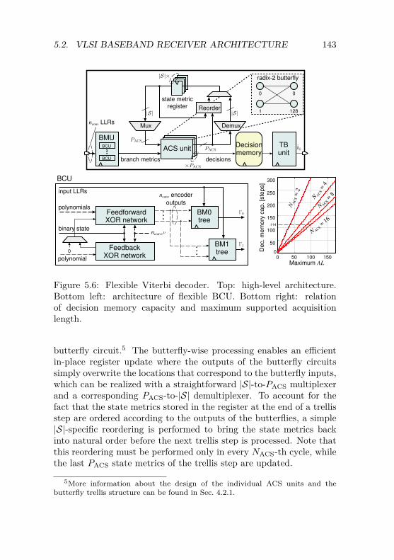
5.2. VLSI BASEBAND RECEIVER ARCHITECTURE 143
ACS unitACS unit
Mux
Reorder
state metricregister
|S|×
×PACS
BMUDecisionmemory
TBunit
|S|
PACS
branch metrics decisions
bkBCU
BCU
nconv
LLRs
PACS
radix-2 butterfly
0 0
1 128|S|
Demux
FeedforwardXOR network
FeedbackXOR network
0
BM0tree
BM1tree
binary state
Γ0
Γ1
nconv
,
polynomial
nconv
encoder
outputs
BCU
polynomials
input LLRs
ν
0 50 100 1500
50
100
150
200
250
300
NA
CS =
2
NA
CS =
4
N ACS
= 8
N AC
S =
16
Maximum ALD
ec.
me
mo
ry c
ap
. [s
tep
s]
114
Figure 5.6: Flexible Viterbi decoder. Top: high-level architecture.Bottom left: architecture of flexible BCU. Bottom right: relationof decision memory capacity and maximum supported acquisitionlength.
butterfly circuit.5 The butterfly-wise processing enables an efficientin-place register update where the outputs of the butterfly circuitssimply overwrite the locations that correspond to the butterfly inputs,which can be realized with a straightforward |S|-to-PACS multiplexerand a corresponding PACS-to-|S| demultiplexer. To account for thefact that the state metrics stored in the register at the end of a trellisstep are ordered according to the outputs of the butterflies, a simple|S|-specific reordering is performed to bring the state metrics backinto natural order before the next trellis step is processed. Note thatthis reordering must be performed only in every NACS-th cycle, whilethe last PACS state metrics of the trellis step are updated.
5More information about the design of the individual ACS units and thebutterfly trellis structure can be found in Sec. 4.2.1.
144 CHAPTER 5. CHANNEL DECODING CHAIN FOR UMTS
Trace-back The bits generated by the ACS units are buffered ina single decision memory. The memory is initially filled with thedecision bits associated with the first AL + W trellis steps, beforethe TB unit starts its operation. Each TB comprises an acquisitionrun of AL steps followed by decoding a window of W steps. Theacquisition run traces the decision memory in backward direction. IfAL is chosen large enough, the TB merges into the ML path and thesubsequent decoding window delivers the next W bits along the MLpath. As opposed to the ACS units, the TB unit processes one fulltrellis step per clock cycle. To enable the concurrent operation of theACS units and the TB unit, the decision memory is realized as two-port RAM and must provide enough capacity to store the decisions ofC = AL + 2W trellis steps. Furthermore, in order to avoid that theACS units have to wait for the TB completion, we require that a TB iscompleted before the ACS units finish the current window, which canonly be realized if AL +W ≤ NACSW . Otherwise, the throughput ofthe architecture would degrade drastically.
The above constraint yields an interesting relation between thedegree of iterative decomposition NACS in the ACS units and thedecision memory capacity C required to support a specific maximumacquisition length. The figure in the lower-right part of Fig. 5.6relates the decision memory capacity to the maximum supported ac-quisition length. It clearly shows that the choice of a large NACSsignificantly reduces the memory requirements compared to a smallNACS = 2. Considering AL = 100, for instance, the decision memorymust provide capacity for 114 trellis steps to allow for continuous ACSprocessing assuming NACS = 16 , whereas it must accommodate upto 300 steps for NACS = 2. Considering a fixed memory capacity of114 steps, the NACS = 2 architecture can only support acquisitionlengths up to AL = 38, which results in a significant performancedegradation6 for highly punctured code rates. Thus, a large degreeof iterative decomposition NACS reduces not only the silicon arearequirements of the ACS computations, but also the decision memoryoverhead.
6According to our simulations performed for the considered convolutionalcodes, AL = 100 is required for a punctured code rate of 0.75. To support veryhigh code rate of 0.95, AL = 180 is required.
5.2. VLSI BASEBAND RECEIVER ARCHITECTURE 145
Figure 5.7: Layout view and chip micrograph of the flexible Viterbidecoder ASIC for UMTS fabricated in (1P/6M) 180 nm CMOS.
Flexible branch metric unit During the sequential processing,the BMU provides the PACS ACS units with the required branchmetrics. To this end, it relies on PACS highly flexible branch metriccomputation units (BCUs) which generate for the associated trellisstates the two output branch metrics. The flexibility requirementsfor different polynomials and nconv is met by programmable XORnetworks that mimic the encoder structure and provide the encoderoutputs based on the binary representation of the associated trellisstate (see lower-left part of Fig. 5.6). The generated encoder outputscontrol two pipelined adder trees which are used to compute thetwo branch metrics (associated with binary-0 and binary-1 encoderinputs, respectively) based on the nconv input LLRs associated withthe currently processed trellis stage. Specifically, the encoder outputsdetermine whether a specific LLR contributes to the branch metricor not. The complexity of the adder trees is given by the maximumsupported nconv.
Stand-alone implementation results Two stand-alone Viterbidecoders have been implemented in 180 nm CMOS to characterizethe VLSI implementation costs associated with the presented flexiblearchitecture. The first design is a straightforward implementation andsupports the complete set of convolutional codes defined in the 3GPPstandard suite with nconv ∈ {2, . . . , 10} and ν ∈ {5, 7, 9}, including therecursive codes used for the adaptive speech traffic channels in GSM or
146 CHAPTER 5. CHANNEL DECODING CHAIN FOR UMTS
the tailbiting7 codes specified for the control channels in LTE/LTE-A.The second design has been further optimized to support exclusivelythe codes specified for UMTS with nconv ∈ {2, 3} and ν = 9. Bothdesigns deploy PACS = 16 ACS units, a 1024 × 16 decision memory,and an LLR input memory to buffer up to 1536 LLR values. The samequantization is used as for the turbo decoders presented in Chapter 4,i.e., the input LLRs are quantized with 5 bit and the state metrics with10 bit (relying on modulo normalization). Based on the second designa prototype has been manufactured and measured; the correspondingchip micrograph is shown in Fig. 5.7.
Table 5.1 shows the key figures of the two implementations. Theall-3GPP solution uses a minimum NACS = 4 to decode the differentcodes. To reduce the area overhead of the BMU, only four BCUssupport the full range of nconv. The other twelve BCUs only sup-port nconv ∈ {2, 3}, which significantly reduces the implementationcomplexity of the adder trees. As expected, the energy efficiency ofthe decoder strongly depends on the constraint length of the code.In particular, for the highest constraint length ν = 9 the decoderrequires roughly the same amount of energy per bit as our SMPbased turbo with I = 8 (see Table 4.4). For lower constraint lengths,the energy efficiency improves considerably, mainly because there isa lower number of states per trellis step and partially because clockgates and input silencing techniques are consistently used to shut-offthe dynamic power consumption of unused resources.
When only UMTS is considered, the architecture can be furtheroptimized. In particular, the BMU can be significantly simplifiedand implemented with a LUT based structure since only one con-straint length ν = 9 and only two different trellis structures (onewith nconv = 2 and the other with nconv = 3) have to be supported.Furthermore, the specification of only one constraint length allows fora complexity reduction in the (de)-multiplexing and reorder networks.
7Tailbiting encoding ensures that the starting state of the encoder is identicalto its ending state, which is realized in a feed-forward encoder by initializingthe shift register with the ν − 1 last information bits of the block. As opposedto the traditional trellis termination approach, tailbiting does not require extratail bits. This property is favorable especially for small block lengths K wheretail bits would become a significant transmission overhead. However, additionalcomplexity is required in the decoder to identify the most likely starting statebefore decoding.
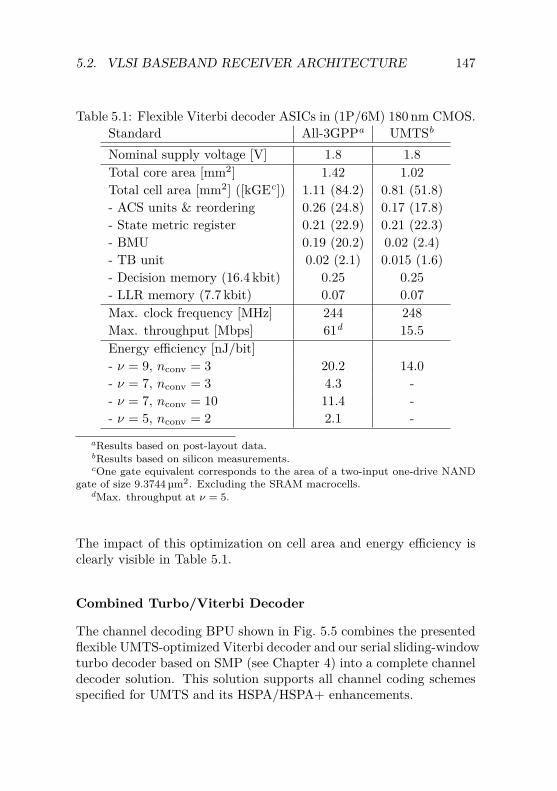
5.2. VLSI BASEBAND RECEIVER ARCHITECTURE 147
Table 5.1: Flexible Viterbi decoder ASICs in (1P/6M) 180 nm CMOS.Standard All-3GPPa UMTSb
Nominal supply voltage [V] 1.8 1.8Total core area [mm2] 1.42 1.02Total cell area [mm2] ([kGEc]) 1.11 (84.2) 0.81 (51.8)- ACS units & reordering 0.26 (24.8) 0.17 (17.8)- State metric register 0.21 (22.9) 0.21 (22.3)- BMU 0.19 (20.2) 0.02 (2.4)- TB unit 0.02 (2.1) 0.015 (1.6)- Decision memory (16.4 kbit) 0.25 0.25- LLR memory (7.7 kbit) 0.07 0.07Max. clock frequency [MHz] 244 248Max. throughput [Mbps] 61d 15.5Energy efficiency [nJ/bit]- ν = 9, nconv = 3 20.2 14.0- ν = 7, nconv = 3 4.3 -- ν = 7, nconv = 10 11.4 -- ν = 5, nconv = 2 2.1 -
aResults based on post-layout data.bResults based on silicon measurements.cOne gate equivalent corresponds to the area of a two-input one-drive NAND
gate of size 9.3744 µm2. Excluding the SRAM macrocells.dMax. throughput at ν = 5.
The impact of this optimization on cell area and energy efficiency isclearly visible in Table 5.1.
Combined Turbo/Viterbi Decoder
The channel decoding BPU shown in Fig. 5.5 combines the presentedflexible UMTS-optimized Viterbi decoder and our serial sliding-windowturbo decoder based on SMP (see Chapter 4) into a complete channeldecoder solution. This solution supports all channel coding schemesspecified for UMTS and its HSPA/HSPA+ enhancements.
148 CHAPTER 5. CHANNEL DECODING CHAIN FOR UMTS
Since only one decoder core is active at a time, the overall memoryoverhead can be reduced significantly by using a single input memoryand a single shared intermediate memory that is accessed by theViterbi and turbo decoder cores to store the decision bits and ex-trinsic LLR values, respectively. The turbo core implements the well-established hard-decision aided (HDA) early termination scheme8 [104]to avoid redundant iterations. In particular, the decoder compares theestimated hard decisions after every iteration and stops decoding if allof them match. To implement the HDA early termination scheme withlow complexity, a 24 bit hash sum generated by a linear feedback shiftregister after every iteration is used as the basis of comparison [75].
5.2.3 Channel Decoding Chain Performance
The performance of the implemented channel decoding chain is stud-ied in Fig. 5.8 using a representative selection of reference measure-ment channel (RMC) types9 and testcases specified by the standard[105]. For the legacy modes, the performance metric is the BLERof the decoded TrBlks at a specific signal-to-interference ratio (SIR)operating point, where the interference represents the interferencefrom other cells modeled as AWGN at the antenna input. For theenhanced modes, the performance metric is given by the receiverdata rate at a given SIR point, taking the performed retransmissionsof the HARQ protocol into account. In order to study the fixed-point performance of the implemented chain independently from thenon-idealities of the equalizer implementation, an ideal floating-pointMMSE equalizer model (with realistic channel estimation, though)has been used for the simulations shown in Fig. 5.8. The implementedchain uses a 5 bit quantization for the LLR values.
8Note that the CRC attached to the individual TrBlks cannot be used asstopping criterion since one TrBlk may be fragmented into several codewords.
9A reference measurement channel specifies a specific transmission mode bydefining the TTI, TrBlk size, timeslots, number of CDMA user codes, modulation,and other parameters. They are specified by the standard as guideline to evaluatereceiver performance.
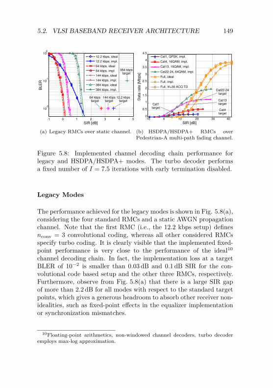
5.2. VLSI BASEBAND RECEIVER ARCHITECTURE 149
-1 0 1 2 3 4 5
10-2
10-1
100
SIR [dB]
BL
ER
12.2 kbps, ideal
12.2 kbps, impl.
64 kbps, ideal
64 kbps, impl.
144 kbps, ideal
144 kbps, impl.
384 kbps, ideal
384 kbps, impl.
12.2 kbpstarget
64 kbpstarget
144 kbpstarget
384 kbpstarget
(a) Legacy RMCs over static channel.
-10 0 10 20 30 400
0.5
1
1.5
2
2.5
3
3.5
4
4.5
SIR [dB]
Da
ta r
ate
[M
bp
s]
Cat1, QPSK, impl.
Cat4, 16QAM, impl.
Cat13, 16QAM, impl.
Cat22-24, 64QAM, impl.
Full, ideal
Full, impl.
Full, W=30 ACQ TD
Cat1target
Cat4target
Cat13target
Cat22-24target
(b) HSDPA/HSDPA+ RMCs overPedestrian-A multi-path fading channel.
Figure 5.8: Implemented channel decoding chain performance forlegacy and HSDPA/HSDPA+ modes. The turbo decoder performsa fixed number of I = 7.5 iterations with early termination disabled.
Legacy Modes
The performance achieved for the legacy modes is shown in Fig. 5.8(a),considering the four standard RMCs and a static AWGN propagationchannel. Note that the first RMC (i.e., the 12.2 kbps setup) definesnconv = 3 convolutional coding, whereas all other considered RMCsspecify turbo coding. It is clearly visible that the implemented fixed-point performance is very close to the performance of the ideal10
channel decoding chain. In fact, the implementation loss at a targetBLER of 10−2 is smaller than 0.03 dB and 0.1 dB SIR for the con-volutional code based setup and the other three RMCs, respectively.Furthermore, observe from Fig. 5.8(a) that there is a large SIR gapof more than 2.2 dB for all modes with respect to the standard targetpoints, which gives a generous headroom to absorb other receiver non-idealities, such as fixed-point effects in the equalizer implementationor synchronization mismatches.
10Floating-point arithmetics, non-windowed channel decoders, turbo decoderemploys max-log approximation.
150 CHAPTER 5. CHANNEL DECODING CHAIN FOR UMTS
Enhanced Modes
Fig. 5.8(b) shows the data rate achieved for a selection of criticalHSDPA/HSDPA+ RMCs over the Pedestrian-A multi-path fadingmobile channel [105]. In addition to the four considered RMCs speci-fied by the standard, we consider also a custom measurement channel(denoted as full in Fig. 5.8(b)) which corresponds to a fully loadedsystem with five timeslots per subframe, 16 assigned CDMA usercodes with 64QAM modulation and high code rate of R = 0.95. Forall setups, the maximum number of HARQ retransmissions is three.
Considering the four standard RMCs, the implemented chain per-forms virtually identically to the ideal chain. Due to this reason,and for the sake of visibility, the ideal performance curves have beenomitted in Fig. 5.8(b). Observe that the data rate targets of thestandard are clearly exceeded for all modes by at least 3 dB.
For the custom measurement channel, we consider in addition tothe ideal and the implemented performance also the floating-pointperformance when a sliding-window turbo decoder based on tradi-tional ACQ with small window length W = 30 is used. Interestingly,the data rate performance of this setup is considerably worse thanthe implemented performance. This observation nicely underlines thediscussion of Chapter 4 and highlights that flexible turbo decoders formodern and emerging wireless systems must be optimized to supportthe full range of code rates in order to avoid serious system-levelperformance degradation.
5.3 VLSI Implementation Results
To prove the applicability and efficiency of the presented digital base-band receiver architecture, a corresponding baseband receiver ASIChas been implemented and taped-out in 130 nm CMOS technology.In what follows, the significant implementation metrics and charac-teristics will be evaluated and discussed with focus on the channeldecoding chain.
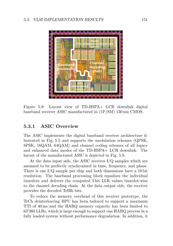
5.3. VLSI IMPLEMENTATION RESULTS 151
Channel decoding
chain
Basebandprocessing
Shared
TrCh deinterleaving/hybrid-ARQ
memory
RF
deinterleaving
memory
Figure 5.9: Layout view of TD-HSPA+ LCR downlink digitalbaseband receiver ASIC manufactured in (1P/8M) 130 nm CMOS.
5.3.1 ASIC Overview
The ASIC implements the digital baseband receiver architecture il-lustrated in Fig. 5.5 and supports the modulation schemes (QPSK,8PSK, 16QAM, 64QAM) and channel coding schemes of all legacyand enhanced data modes of the TD-HSPA+ LCR downlink. Thelayout of the manufactured ASIC is depicted in Fig. 5.9.
At the data input side, the ASIC receives I/Q samples which areassumed to be perfectly synchronized in time, frequency, and phase.There is one I/Q sample per chip and both dimensions have a 10 bitresolution. The baseband processing block equalizes the individualtimeslots and delivers the computed 5 bit LLR values timeslot-wiseto the channel decoding chain. At the data output side, the receiverprovides the decoded TrBlk bits.
To reduce the memory overhead of this receiver prototype, theTrCh deinterleaving BPU has been tailored to support a maximumTTI of 40 ms and the HARQ memory capacity has been limited to63’360 LLRs, which is large enough to support one HARQ process in afully loaded system without performance degradation. In addition, it
152 CHAPTER 5. CHANNEL DECODING CHAIN FOR UMTS
is assumed that only one CCTrCh is active in any TTI, which enablesone to realize the TrCh deinterleaver memory and HARQ memorywith a single shared memory block (see Fig. 5.9). Furthermore, onlytwo multiplexed TrChs are supported per CCTrCh. We emphasizethat the implemented configuration supports all legacy RMC typesand all enhanced RMCs [105] with the practical prototype constraintof limited HARQ memory size.
The ASIC occupies a total core area of 7.21 mm2 and achievesat nominal supply voltage of 1.2 V a maximum operating clock fre-quency11 of 180 MHz, which is well above the minimum requiredfrequency of 85 MHz. This minimum frequency is defined by theworst-case processing delay of the turbo decoder at I = 7.5 iterationsrequired to process an (imaginary) 5 ms TTI where all six downlinktimeslots are loaded with 16 assigned CDMA codes at R = 1 and64QAM modulation. The large speed overhead enables one to keepbuffer sizes small and additionally apply voltage scaling to reduceenergy dissipation.
5.3.2 Results and DiscussionSilicon Area
A detailed cell-area breakdown of the ASIC is provided in Table 5.2.Observe that 60% of the overall receiver cell area is occupied by SRAMmemory. As expected, most memory resources (85%) are located inthe channel decoding chain. Considering only the logic cell area (i.e.,the cell area without the SRAM macrocells), it can be seen that thechannel decoding chain requires roughly the same amount of hardwareresources as the baseband processing block.
Within the channel decoding chain, the overall cell area is domi-nated by the memories required to realize the two deinterleaving stagesand the HARQ functionality. Apart from these large memories, thechannel decoding BPU clearly dominates and occupies 70% of thechain, while 15% of the remaining area is attributed to the logic cellarea of the two deinterleaving stages and Hybrid-ARQ BPUs, and11% to the control unit. The logic area of the deinterleaving and
11The maximum clock frequency is estimated based on post-layout data.
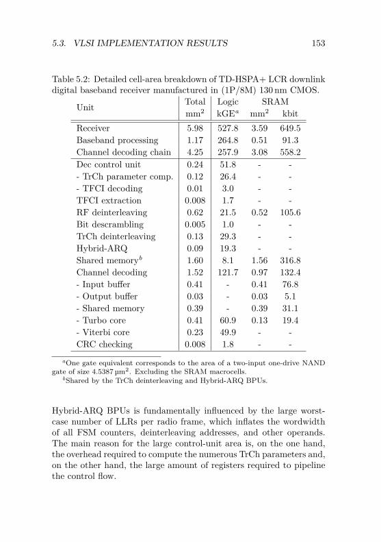
5.3. VLSI IMPLEMENTATION RESULTS 153
Table 5.2: Detailed cell-area breakdown of TD-HSPA+ LCR downlinkdigital baseband receiver manufactured in (1P/8M) 130 nm CMOS.
Unit Total Logic SRAMmm2 kGEa mm2 kbit
Receiver 5.98 527.8 3.59 649.5Baseband processing 1.17 264.8 0.51 91.3Channel decoding chain 4.25 257.9 3.08 558.2Dec control unit 0.24 51.8 - -- TrCh parameter comp. 0.12 26.4 - -- TFCI decoding 0.01 3.0 - -TFCI extraction 0.008 1.7 - -RF deinterleaving 0.62 21.5 0.52 105.6Bit descrambling 0.005 1.0 - -TrCh deinterleaving 0.13 29.3 - -Hybrid-ARQ 0.09 19.3 - -Shared memoryb 1.60 8.1 1.56 316.8Channel decoding 1.52 121.7 0.97 132.4- Input buffer 0.41 - 0.41 76.8- Output buffer 0.03 - 0.03 5.1- Shared memory 0.39 - 0.39 31.1- Turbo core 0.41 60.9 0.13 19.4- Viterbi core 0.23 49.9 - -CRC checking 0.008 1.8 - -
aOne gate equivalent corresponds to the area of a two-input one-drive NANDgate of size 4.5387 µm2. Excluding the SRAM macrocells.
bShared by the TrCh deinterleaving and Hybrid-ARQ BPUs.
Hybrid-ARQ BPUs is fundamentally influenced by the large worst-case number of LLRs per radio frame, which inflates the wordwidthof all FSM counters, deinterleaving addresses, and other operands.The main reason for the large control-unit area is, on the one hand,the overhead required to compute the numerous TrCh parameters and,on the other hand, the large amount of registers required to pipelinethe control flow.
154 CHAPTER 5. CHANNEL DECODING CHAIN FOR UMTS
Interestingly, the described intermediate-memory sharing insidethe channel decoding BPU allows one to support the large constraint-length convolutional code with low overhead in addition to the turbomodes. In particular, as can be seen from Table 5.2, the Viterbi coreoccupies only 15% of the overall channel decoding cell area.
Power Consumption
The power consumption, energy dissipation, and energy efficiency interms of energy per TrBlk bit of the implemented channel decodingchain are shown in Table 5.3 for different HSDPA/HSDPA+ measure-ment channels. In particular, we consider the fully loaded setup inaddition to the less complex Cat22-24 and Cat1 standard RMCs. Allmeasurement channels specify a 5 ms TTI and turbo coding. For allthree considered setups, the power measurement has been performedover the full TTI.
Clearly, the fully loaded setup consumes most power and conse-quently requires most energy per TTI. More interestingly, however,observe from Table 5.3 that the power consumption of the modes withlower load decreases drastically. This large power reduction for thelower-complexity modes can be attributed partially to the fact thatthe processing delay of the individual BPUs in the proposed channeldecoding chain architecture nicely scales with the load of the processedmodes and partially to our efficient clock gating strategy that ensuresthat the clock signal of a BPU is turned off as soon as it becomesstalled or idle.
The second part of Table 5.3 shows the detailed energy-efficiencybreakdown obtained for the fully loaded measurement channel. In-terestingly, the table reveals that the major part (75%) of the energyis dissipated inside the channel decoder. The remaining BPUs andthe control unit, including the processor-like computation of the TrChparameters, amount to less than 11% of the overall energy dissipation.This observation allows one to conclude that the presented channeldecoding chain VLSI architecture provides the required flexibility withvery low power overhead. When the implemented HDA early ter-mination scheme is enabled, the average energy dissipation insidethe turbo decoder decreases, making the share of the other unitsmore pronounced, but also leading to an overall energy efficiency
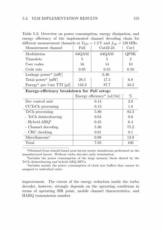
5.3. VLSI IMPLEMENTATION RESULTS 155
Table 5.3: Overview on power consumption, energy dissipation, andenergy efficiency of the implemented channel decoding chain fordifferent measurement channels at VDD = 1.2 V and fclk = 128 MHz.
Measurement channel Full Cat22-24 Cat1Modulation 64QAM 64QAM QPSKTimeslots 5 5 2User codes 16 14 10Code rate 0.95 0.55 0.58Leakage powera [mW] 0.40Total powera [mW] 28.5 17.5 6.8Energya per 5 ms TTI [µJ] 142.3 87.7 34.2Energy-efficiency breakdown for Full setup:
Energy efficiencya [nJ/bit] %Dec control unit 0.14 2.0CCTrCh processing 0.13 1.8TrCh processing 5.80 82.3- TrCh deinterleaving 0.04 0.6- Hybrid-ARQb 0.45 6.4- Channel decoding 5.30 75.2- CRC checking 0.01 0.1Miscellaneousc 0.98 13.9Total 7.05 100aObtained from stimuli-based post-layout power simulations performed on the
manufactured layout. Without turbo decoder early termination.bIncludes the power consumption of the large memory block shared by the
TrCh deinterleaving and hybrid-ARQ BPUs.cIncludes mainly the power consumption of clock tree buffers that cannot be
assigned to individual units.
improvement. The extent of the energy reduction inside the turbodecoder, however, strongly depends on the operating conditions interms of operating SIR point, mobile channel characteristics, andHARQ transmission number.

Chapter 6
Summary andConclusion
High-performance low-density parity-check (LDPC) codes and turbocodes have become key ingredients for achieving the high throughputand the challenging quality-of-service (QoS) requirements of currentand emerging next-generation wireless communication systems. Theexcellent error-correction capabilities of these codes, however, comeat the expense of substantial computational burden at the receiverdue to highly sophisticated iterative algorithms that are required fordecoding. For this reason, corresponding channel decoders must beimplemented as application-specific VLSI circuits in order to leveragethe area and power advantage of circuits implemented in dedicatedhardware. In addition to the high signal processing complexity, ithas been shown that corresponding practical VLSI decoder solutionsmust provide a high degree of flexibility to support the numerousmodes of operation in terms of block length and code rate. Thiscontradicting combination of flexibility demands and computationalcomplexity renders the efficient implementation of channel decoders akey challenge faced by designers of digital wireless baseband receivers.
In this thesis, we have investigated the area- and energy-efficientASIC design of quasi-cyclic (QC) LDPC and turbo channel decodersthat are able to support the full range of throughput and flexibility
157
158 CHAPTER 6. SUMMARY AND CONCLUSION
requirements of current and emerging wireless systems. To completethe picture of flexible channel decoding circuits for wireless systems,the thesis also explores the VLSI implementation challenges associatedwith complete channel decoding chains. In general, the proposedconcepts and solutions presented throughout this thesis underline thatcareful joint optimization of algorithm-level, architecture-level, andcircuit-level aspects is key for the design of efficient flexible VLSIcircuits for channel decoding, even under the consideration of recentvery deep-submicron CMOS technology nodes.
Algorithm Selection
The underlying iterative decoding algorithms for LDPC codes andturbo codes have been carefully selected with respect to their suit-ability for VLSI implementation. The selected algorithms for thesetwo classes of channel codes are based on different graphical repre-sentations that drive the designer to very code-specific VLSI architec-tures and distinct approaches to cope with the challenging flexibilitydemands.
In particular, LDPC codes are typically represented from the view-point of their parity-check constraints, and decoding is performed onthe associated factor graph. The layered offset-min-sum message-passing algorithm has been identified as particularly suitable for VLSIimplementation. Turbo codes, in contrast, are represented from thepoint of view of their trellis constraints, where iterative message-passing coincides with iterative soft-input soft-output (SISO) decod-ing of the concatenated component codes. The max-log approxi-mated BCJR SISO algorithm and an improved soft-output Viterbialgorithm (SOVA) have been selected as low-complexity decodingalgorithm candidates.
Flexible QC-LDPC Decoders
The message-passing algorithm inherently offers an extremely highdegree of parallelism, and it has been shown that corresponding VLSIarchitectures can be tuned for very different area/throughput trade-offs through iterative decomposition of the message update compu-tations and resource sharing among nodes in the factor graph. In
159
order to provide flexibility for different block lengths and code rates,practical decoder implementations for wireless systems must supporta wide range of different parity-check matrices. The block-parallelarchitecture class, which processes the parity-check matrix block-wise,has been identified as a particularly suitable solution to enable thisflexibility, especially in conjunction with QC-LDPC codes. By tuningthe number of blocks processed per clock cycle, this architecture classsupports the full range of throughput requirements found in modernwireless standards, including multiple-Gbps as required by emergingsystems. Based on this block-parallel architecture class, an efficientQC-LDPC decoder architecture has been presented. The architectureprovides the flexibility to support virtually all parity-check matricesthat fit into the allocated hardware resources. Interestingly, it hasbeen shown that this high degree of flexibility comes at low areaoverhead and is realized by the use of an optimized cyclic shifterimplementation and by following a simple low-complexity control flowwhere the individual hardware units are controlled based on a controlsequence stored in a controller memory.
The message memory components, which have to support veryhigh data bandwidth, have been identified as a fundamental powerbottleneck in block-parallel QC-LDPC decoder implementations. Inorder to alleviate this bottleneck, a low-power standard-cell basedmemory (SCM) architecture has been proposed. The memory ar-chitecture has been carefully optimized on architecture- and circuit-level to reduce the number of memory access cycles and to limitdynamic power consumption per read/write access as far as possible.Beside the lower dynamic power consumption, another fundamentalkey advantage of the use of the proposed SCMs over the use of SRAMmacrocells is the fact that SCMs can be partitioned in a very fine-grained manner, enabling designers to maintain the high data localityof the message-passing algorithm. The individual partitions can beturned on and off separately, which is key to enable good energyefficiency also for small block lengths.
The architecture has been optimized for the IEEE 802.11n WLANstandard and manufactured in 90 nm CMOS technology relying oncommercial standard-cells. The corresponding measurement resultsdemonstrate that the proposed concepts and solutions lead to excel-lent energy efficiency (clearly outperforming prior-art decoders) and
160 CHAPTER 6. SUMMARY AND CONCLUSION
highly competitive silicon efficiency, while supporting all operationmodes and exceeding the high-throughput requirements of the stan-dard. The reported results further display that the flexibility providedby our block-parallel QC-LDPC decoder architecture does not lead toany performance penalty in terms of area, throughput or power. Apotential drawback of SCM based memory components is the fact thatcommercial standard-cells typically provide only static latches whichgenerally lead to worse area efficiency than SRAM macrocells for largememory capacities. However, it has been shown that the uniquememory update statistics in block-parallel QC-LDPC decoders canbe exploited to replace the static latches by high-density refresh-freedynamic latches, enabling one to mitigate the penalty in area efficiencyassociated with SCMs to a large extent. In fact, the silicon area ofSCM based QC-LDPC decoders targeting the IEEE 802.11n WLANstandard can be reduced by 45% when relying on custom-designeddynamic latches as storage cells.
Flexible Turbo Decoders
The VLSI implementation complexity of flexible sliding-window turbodecoders has been thoroughly investigated, considering both serialand subblock-parallel architectures. These two architecture typesenable very different throughput/area trade-offs that can be tailoredto the specifics of the considered wireless standard. The serial radix-2turbo decoder architecture lies on the low-throughput end of thearchitecture’s portfolio and, thus, qualifies for standards with rela-tively moderate throughput requirements (such as 3GPP’s enhanced-2G and 3G standards). Despite its low throughput, this architec-ture type is attractive due to its low silicon area and its propertyof supporting general non-contention-free interleavers without anyoverhead. Subblock-parallel architectures, in contrast, enable veryhigh throughput, but require contention-free interleavers (such as theQPP interleaver specified for LTE and LTE-A) for economic imple-mentation. Compared to LDPC decoders, however, the degree ofparallelism in practical turbo decoder implementations is limited, and
161
large degrees of subblock-parallelism come with diminishing through-put returns. This parallel turbo-decoder predicament is a fundamen-tal performance bottleneck in sliding-window subblock-parallel turbodecoders.
The implementation of turbo decoders that support the full rangeof flexibility requirements of wireless standards is associated withhigher costs in terms of both design effort and silicon overhead asit is the case for QC-LDPC decoders. In particular, the constraintof supporting strongly punctured code rates has been revealed asa fundamental issue in practical sliding-window turbo decoders. Infact, this thesis shows that the constraint of high code rate stronglyaffects the architectural choices for SISO decoding in turbo decoders,and that considering other choices than the well-known conventionalapproach is key to arrive at economic implementations.
Serial turbo decoders Since throughput is typically not a mainconcern in serial turbo decoders, we have focused on radix-2 trellis pro-cessing with a fixed number of iterations that is large enough to enablealmost saturated error-rate performance. The thesis shows that theconventional sliding-window BCJR architecture based on acquisitionruns (ACQ) suffers from exploding window lengths required to sustaina competitive error-rate performance when high code rate has to besupported. The large window lengths lead to augmented memoryrequirements that substantially rise the implementation costs. Theless prominent BCJR architecture based on state metric propaga-tion (SMP), in contrast, leads to good error-rate performance withfairly small window lengths (i.e., comparably low memory overhead)over the full range of code rates, but does so with a slightly reducedconvergence speed compared to ACQ. Since flexible BCJR decodersgenerally suffer from a large memory overhead, an effort has been putinto devising memory compressing techniques for the two large Alphaand SMP memories. The presented compression techniques proveto be especially effective in serial radix-2 turbo decoders and enablemore than 10% area savings without any degradation in error-rateperformance.
Flexible turbo decoders based on both BCJR architecture typesoptimized for the UMTS HSPA downlink have been implemented in
162 CHAPTER 6. SUMMARY AND CONCLUSION
180 nm CMOS technology. Corresponding post-layout implementa-tion results clearly demonstrate that the SMP based decoder signif-icantly outperforms the ACQ based one in terms of silicon area andsilicon efficiency with lower power consumption (and consequentlylower energy per bit per iteration). The ACQ based decoder exhibitsa potential advantage in terms of average energy per bit due to itsfaster convergence speed, which, however, can only be realized incertain operating conditions with early termination employed. Theseobservations lead to the general conclusion that SMP based BCJRdecoders are most suited for the implementation of flexible serial turbodecoders.
Based on the presented improved SOVA, a highly efficient SOVAdecoder architecture relying on register-exchange (RE) computationshas been designed and implemented. With this SOVA decoder, SOVAbased turbo decoders generally become a competitive alternative toBCJR based turbo decoders. In fact, when only weakly puncturedcode rates are considered, the SOVA leads to smaller and more energy-efficient turbo decoder implementations, while the difference in termsof error-rate performance is negligible. Interestingly, the large imbal-ance of signal-path delays inside RE based SOVA decoders allows foran efficient power domain partitioning, enabling substantial energysavings through voltage scaling without sacrificing any throughput orerror-rate performance. When high code rate has to be supported,however, the silicon area of the RE unit required to trace the concur-rent paths explodes, rendering SOVA based turbo decoders generallyimpractical for this operating condition.
Subblock-parallel turbo decoders For subblock-parallel turbodecoders, a novel framework has been proposed that allows for asystematic comparison of sliding-window architectures, taking intoaccount their individual trade-offs in terms of window length, error-rate performance, performed turbo iterations, and throughput. Usingthis framework, it has been shown that the choice of the SISO decoderarchitecture has a significant impact not only on silicon area andpower consumption of the turbo decoder, but also on throughput.The impact on throughput is especially strong for high code rate andlarge degrees of subblock-parallelism where the parallel turbo-decoder
163
predicament becomes strongly pronounced. In particular, when onlyweakly punctured code rates are considered, subblock-parallel turbodecoders based on ACQ achieve higher throughput than decodersbased on SMP, mainly due to their higher convergence speed. For highcode rate, on the other hand, the throughput of ACQ based decoderscollapses for larger degrees of subblock-parallelism as a consequenceof exploding window length.
To alleviate the parallel turbo-decoder predicament, an optimizedSISO decoder architecture has been proposed, combining the high con-vergence speed of ACQ with the benefit of state metric initializationacross iterations as provided by SMP. The described trade-off studyin 65 nm CMOS technology demonstrates that the combined SISOdecoder architecture, referred to as SMP-assisted ACQ (SAA), notonly enables substantially higher turbo decoder throughput than theother two architecture types for all code rates, but also displays bestsilicon efficiency. Based on this optimized SISO decoder architecture,a subblock-parallel turbo decoder employing 16 SISO decoder coresoptimized for the LTE-A standard has been manufactured in 65 nmCMOS. The decoder achieves unprecedented measured throughputabove 1 Gbps for all code rates and outperforms the prior-art imple-mentations in both energy efficiency and silicon efficiency.
We emphasize at this point that the application of the SAA basedSISO decoder architecture in serial turbo decoders under considera-tion of a fixed number of iterations turns out to be rather unattractiveas it results in significantly more silicon area and higher power con-sumption than SMP [90].
Complete Channel Decoding Chain for UMTS
The high-performance channel decoders in baseband receivers for mod-ern and emerging wireless systems are typically embedded in a sophis-ticated channel decoding chain. In this thesis, the VLSI implementa-tion challenges and costs associated with the downlink channel decod-ing chain for the representative enhanced 3G TD-SCDMA standardhave been studied in detail. In general, the investigations reveal thata substantial design effort in addition to the described stand-alonechannel decoder implementations is necessary in order to implementthe complete channel decoding chain in fully dedicated hardware that
164 CHAPTER 6. SUMMARY AND CONCLUSION
meets the stringent flexibility requirements of the standard with lowarea and power overhead. The presented VLSI architecture providesthe demanded flexibility by partitioning the channel decoding chaininto independent basic processing units (BPU). These BPUs have beencarefully optimized for low area overhead and for a highly regularand simple control flow by exploiting identified commonalities andregularities among the different operation modes of the chain.
To support the specified convolutional codes in addition to turbocodes with low overhead, a highly efficient flexible Viterbi decoderarchitecture has been designed. The proposed architecture supportsa wide range of trellis structures and area/throughput trade-offs thatcan be tailored to the application at hand. The high flexibility of thearchitecture is enabled by following a sequential processing approachwith a large degree of iterative decomposition in the ACS computa-tions. The Viterbi decoder has been combined together with an SMPbased serial radix-2 turbo decoder to form a complete channel decodersolution with optimized memory sharing among the two decoder cores.
The proposed concepts and channel decoding chain architecturehave been proved in a complete downlink digital baseband receiverimplementation in 130 nm CMOS technology. The post-layout imple-mentation results show that the memory overhead required to supportthe large worst-case interleaver depths and hybrid-ARQ functionalitydominates the silicon area of the channel decoding chain and rep-resents a large fraction of the overall receiver area. The power con-sumption of the channel decoding chain, however, is clearly dominatedby the channel decoder and scales with the load of the processedoperation mode. The results further demonstrate that the proposedsequential Viterbi decoder architecture allows one to support the chal-lenging 256-state convolutional codes specified in recent standards inaddition to the turbo decoder with less than 20% area overhead.
In summary, the provided results underline the efficiency of theproposed channel decoding chain architecture and lead to the generalimportant conclusion that a fully dedicated VLSI implementation isable to deliver high area- and power efficiency despite the countlessoperation modes that must be supported.
Acronyms
3GPP third-generation partnership project
ACQ acquisition runACS add-compare-selectASIC application-specific integrated circuitAWGN additive white Gaussian noise
BER bit error-rateBLER block error-rateBMU branch metric unitBPSK binary phase shift keyingBPU basic processing unit
CCTrCh coded composite TrChCDMA code-division multiple accessCMOS complementary metal-oxide semiconductorCN check nodeCNU check node unitCRC cyclic redundancy checkCS cyclic shifter
D-SCM dynamic SCMDVB-S2 digital video broadcasting - satellite - second generation
165
166 Acronyms
E-EDGE evolved EDGEEDGE enhanced data rates for GSM evolution
FSM finite state machine
GPRS general packet radio serviceGSM global system for mobile communications
HARQ hybrid automatic repeat requestHDA hard-decision aidedHSDPA high-speed downlink packet accessHSPA high-speed packet accessHSPA+ evolved HSPA
IEEE institute of electrical and electronics engineers
LCR low chip rateLDPC low-density parity-checkLLR log-likelihood ratioLTE long-term evolutionLTE-A LTE advanced
MAP maximum a-posterioriMIMO multiple-input multiple-outputMMSE minimum mean square error
NCU node computation unit
OMS offset-min-sum
PhCh physical channelPPC partial parity check
Acronyms 167
QAM quadrature amplitude modulationQC quasi-cyclicQPP quadratic permutation polynomialQPSK quadrature phase shift keying
RAM random-access memoryRE register-exchangeREU register-exchange unitRMC reference measurement channel
SAA SMP-assisted ACQSCM standard-cell based memorySIR signal-to-interference ratioSISO soft-input soft-outputSMP state metric propagationSMU state metric unitSNR signal-to-noise ratioSOVA soft-output Viterbi algorithmSRAM static RAM
TB trace-backTDD time-division duplexTD-HSPA time-division HSPATDMA time-division multiple accessTD-SCDMA time-division synchronous CDMATFCI transport format combination indicatorTrBlk transport blockTrCh transport channelTTI transmission time interval
UMTS universal mobile telecommunications system
VLSI very-large-scale integrationVN variable node
168 Acronyms
VNU variable node unit
WCDMA wideband CDMAWiGig wireless gigabitWiMAX worldwide interoperability for microwave accessWLAN wireless local area networkWMAN wireless metropolitan area network
Bibliography
[1] “Measuring the information society (report),” InternationalTelecommunication Union (ITU), Geneva, Switzerland, 2014,available online at http://www.itu.int.
[2] S. Cherry, “Edholm’s law of bandwidth,” IEEE Spectrum,vol. 41, no. 7, pp. 58–60, Jul. 2004.
[3] G. Caire, G. Taricco, and E. Biglieri, “Bit-interleaved codedmodulation,” IEEE Trans. Inf. Theory, vol. 44, no. 3, pp. 927–946, May 1998.
[4] R. Gallager, “Low-density parity-check codes,” IRE Trans. Inf.Theory, vol. 8, no. 1, pp. 21–28, Jan. 1962.
[5] J. Proakis, Digital Communications, 5th ed. McGraw-Hill,2007.
[6] A. Viterbi, “Error bounds for convolutional codes and anasymptotically optimum decoding algorithm,” IEEE Trans. Inf.Theory, vol. 13, no. 2, pp. 260–269, Apr. 1967.
[7] C. Berrou, A. Glavieux, and P. Thitimajshima, “Near shannonlimit error-correcting coding and decoding: Turbo-codes,” inProc. IEEE Int. Conf. Commun., May 1993, pp. 1064–1070.
[8] D. J. C. MacKay, “Good error-correcting codes based on verysparse matrices,” IEEE Trans. Inf. Theory, vol. 45, no. 2, pp.399–431, Mar. 1999.
169
170 BIBLIOGRAPHY
[9] T. Richardson and R. Urbanke, Modern Channel Coding The-ory. Cambridge University Press, 2008.
[10] N. Wiberg, H.-A. Loeliger, and R. Kotter, “Codes and iterativedecoding on general graphs,” Europ. Trans. Telecommun.,vol. 6, pp. 513–525, Sep. 1995.
[11] F. Kschischang, B. Frey, and H.-A. Loeliger, “Factor graphs andthe sum-product algorithm,” IEEE Trans. Inf. Theory, vol. 47,no. 2, pp. 498–519, Feb. 2001.
[12] H.-A. Loeliger, “An introduction to factor graphs,” IEEE SignalProcess. Mag., vol. 21, no. 1, pp. 28–41, Jan. 2004.
[13] C. Roth, D. Stadelmann, C. Benkeser, and Q. Huang, “High-throughput hardware decoder implementation for deep-spaceoptical communications,” in Proc. ESA Int. Workshop on Track-ing, Telemetry, and Command Systems for Space Applications,Sep. 2013.
[14] N. Walenta, A. Burg, D. Caselunghe, J. Constantin, N. Gisin,O. Guinnard, R. Houlmann, P. Junod, B. Korzh, N. Kuleszaet al., “A fast and versatile quantum key distribution systemwith hardware key distillation and wavelength multiplexing,”New Journal of Physics, vol. 16, 2014.
[15] A. Cevrero, Y. Leblebici, P. Ienne, and A. Burg, “A 5.35 mm210GBASE-T Ethernet LDPC decoder chip in 90 nm CMOS,”in Proc. IEEE Asian Solid-State Circuits Conf., Nov. 2010, pp.317–320.
[16] Y. Kou, S. Lin, and M. Fossorier, “Low-density parity-checkcodes based on finite geometries: a rediscovery and new results,”IEEE Trans. Inf. Theory, vol. 47, no. 7, pp. 2711–2736, Nov.2001.
[17] M. Fossorier, “Quasicyclic low-density parity-check codes fromcirculant permutation matrices,” IEEE Trans. Inf. Theory,vol. 50, no. 8, pp. 1788–1793, Aug. 2004.
BIBLIOGRAPHY 171
[18] H. Kaeslin, Digital Integrated Circuit Design, 1st ed. Cam-bridge University Press, 2008.
[19] C. Benkeser, “Power efficiency and the mapping of communi-cation algorithms into VLSI,” Ph.D. dissertation, IntegratedSystems Laboratory, ETH Zurich, Switzerland, 2008.
[20] M. Horowitz, “Computing’s energy problem (and what we cando about it),” in Proc. IEEE Int. Solid-State Circuits Conf., Feb2014, pp. 10–14.
[21] C. Roth, P. Meinerzhagen, C. Studer, and A. Burg, “A 15.8pj/bit/iter quasi-cyclic LDPC decoder for IEEE 802.11n in90 nm CMOS,” in Proc. IEEE Asian Solid-State Circuits Conf.,Nov. 2010, pp. 313–316.
[22] C. Roth, A. Cevrero, C. Studer, Y. Leblebici, and A. Burg,“Area, throughput, and energy-efficiency trade-offs in the VLSIimplementation of LDPC decoders,” in Proc. IEEE Int. Symp.Circuits and Systems, May 2011, pp. 1772–1775.
[23] P. Meinerzhagen, C. Roth, and A. Burg, “Towards generic low-power area-efficient standard cell based memory architectures,”in Proc. IEEE Int. Midwest Symp. Circuits and Systems, Aug.2010, pp. 129–132.
[24] P. Meinerzhagen, A. Bonetti, G. Karakonstantis, C. Roth,F. Gurkaynak, and A. Burg, “Refresh-free dynamic standard-cell based memories: Application to a QC-LDPC decoder,” inProc. IEEE Int. Symp. Circuits and Systems, May 2015, pp.1426–1429.
[25] C. Benkeser, C. Roth, and Q. Huang, “Turbo decoder designfor high code rates,” in Proc. IFIP/IEEE Int. Conf. Very LargeScale Integration, Oct. 2012, pp. 71–75.
[26] S. Belfanti, C. Roth, M. Gautschi, C. Benkeser, and Q. Huang,“A 1Gbps LTE-advanced turbo-decoder ASIC in 65 nm CMOS,”in Proc. Symp. VLSI Circuits, Jun. 2013, pp. C284–C285.
172 BIBLIOGRAPHY
[27] C. Roth, S. Belfanti, C. Benkeser, and Q. Huang, “Efficientparallel turbo-decoding for high-throughput wireless systems,”IEEE Trans. Circuits Syst. I, vol. 61, no. 6, pp. 1824–1835, May2014.
[28] C. Roth, C. Benkeser, and Q. Huang, “Power-efficient turbo-decoder design based on algorithm-specific power domain par-titioning,” in Proc. IEEE Int. Workshop on Power and TimingModeling, Optimization and Simulation, Sep. 2014.
[29] J. Hagenauer, E. Offer, and L. Papke, “Iterative decodingof binary block and convolutional codes,” IEEE Trans. Inf.Theory, vol. 42, no. 2, pp. 429–445, Mar. 1996.
[30] L. Bahl, J. Cocke, F. Jelinek, and J. Raviv, “Optimal decodingof linear codes for minimizing symbol error rate,” IEEE Trans.Inf. Theory, vol. 20, no. 2, pp. 284–287, Mar. 1974.
[31] R. Tanner, “A recursive approach to low complexity codes,”IEEE Trans. Inf. Theory, vol. 27, no. 5, pp. 533–547, Sep. 1981.
[32] K. Gunnam, G. Choi, W. Wang, E. Kim, and M. Yeary,“Decoding of quasi-cyclic LDPC codes using an on-the-flycomputation,” in Proc. Asilomar Conf. Signals, Systems andComputers, Oct. 2006, pp. 1192–1199.
[33] IEEE Std 802.11n-2009–Amendment 5: Enhancements forHigher Throughputs, IEEE-SA, Oct. 2009.
[34] IEEE Std 802.16-2009: Air Interface for Fixed BroadbandWireless Access Systems, IEEE-SA, May 2009.
[35] E. Sharon, S. Litsyn, and J. Goldberger, “An efficient message-passing schedule for LDPC decoding,” in Proc. IEEE Conv.Electrical and Electronics Engineers in Israel, Sep. 2004, pp.223–226.
[36] M. P. C. Fossorier, M. Mihaljevic, and H. Imai, “Reducedcomplexity iterative decoding of low-density parity check codesbased on belief propagation,” IEEE Trans. Commun., vol. 47,no. 5, pp. 673–680, May 1999.
BIBLIOGRAPHY 173
[37] J. Chen, A. Dholakia, E. Eleftheriou, M. P. C. Fossorier, and X.-Y. Hu, “Reduced-complexity decoding of LDPC codes,” IEEETrans. Commun., vol. 53, no. 7, pp. 1288–1299, Aug. 2005.
[38] Multiplexing and Channel Coding (TDD), 3GPP TS 25.222,Rev. 12.0.0, Dec. 2013.
[39] Evolved Universal Terrestrial Radio Access (E-UTRA); Multi-plexing and channel coding, 3GPP TS 36.212, Rev. 12.2.0, Sep.2014.
[40] J. Sun and O. Takeshita, “Interleavers for turbo codes usingpermutation polynomials over integer rings,” IEEE Trans. Inf.Theory, vol. 51, no. 1, pp. 101–119, Jan. 2005.
[41] J. Hagenauer and P. Hoeher, “A Viterbi algorithm with soft-decision outputs and its applications,” in Proc. IEEE GlobalCommun. Conf., Nov. 1989, pp. 1680–1686.
[42] P. Robertson, E. Villebrun, and P. Hoeher, “A comparison ofoptimal and sub-optimal MAP decoding algorithms operatingin the log domain,” in Proc. IEEE Int. Conf. Commun., vol. 2,Jun. 1995, pp. 1009–1013.
[43] M. Fossorier, F. Burkert, S. Lin, and J. Hagenauer, “Onthe equivalence between SOVA and max-log-MAP decodings,”IEEE Commun. Lett., vol. 2, no. 5, pp. 137–139, May 1998.
[44] L.-H. Ang, W.-G. Lim, and M. Kamuf, “Modification of SOVA-based algorithms for efficient hardware implementation,” inProc. IEEE Veh. Technol. Conf., May 2010.
[45] J. Woodard and L. Hanzo, “Comparative study of turbodecoding techniques: An overview,” IEEE Trans. Veh. Technol.,vol. 49, no. 6, pp. 2208–2233, Nov. 2000.
[46] J. Vogt and A. Finger, “Improving the max-log-MAP turbodecoder,” Electron. Lett., vol. 36, no. 23, pp. 1937–1939, Nov.2000.
174 BIBLIOGRAPHY
[47] L. Papke, P. Robertson, and E. Villebrun, “Improved decodingwith the SOVA in a parallel concatenated (turbo-code) scheme,”in Proc. IEEE Int. Conf. Commun., Jun. 1996, pp. 102–106.
[48] M. Weiner, B. Nikolic, and Z. Zhang, “LDPC decoder architec-ture for high-data rate personal-area networks,” in Proc. IEEEInt. Symp. Circuits and Systems, May 2011, pp. 1784–1787.
[49] A. J. Blanksby and C. J. Howland, “A 690-mW 1-Gb/s 1024-b,rate-1/2 low-density parity-check code decoder,” IEEE J. Solid-State Circuits, vol. 37, no. 3, pp. 404–412, Mar. 2002.
[50] A. Darabiha, A. C. Carusone, and F. R. Kschischang, “A3.3-Gbps bit-serial block-interlaced min-sum LDPC decoder in0.13 µm CMOS,” in Proc. Custom Integrated Circuits Conf.,Sep. 2007, pp. 459–462.
[51] N. Onizawa, T. Hanyu, and V. C. Gaudet, “Design of high-throughput fully parallel LDPC decoders based on wire parti-tioning,” IEEE Trans. VLSI Syst., vol. 18, no. 3, pp. 482–489,Mar. 2010.
[52] T. Mohsenin, D. N. Truong, and B. M. Baas, “A low-complexitymessage-passing algorithm for reduced routing congestion inLDPC decoders,” IEEE Trans. Circuits Syst. I, vol. 57, no. 5,pp. 1048–1061, May 2010.
[53] A. Darabiha, A. C. Carusone, and F. R. Kschischang, “Block-interlaced LDPC decoders with reduced interconnect complex-ity,” IEEE Trans. Circuits Syst. II, vol. 55, no. 1, pp. 74–78,Jan. 2008.
[54] L. Liu and C.-J. Shi, “Sliced message passing: high through-put overlapped decoding of high-rate low-density parity-checkcodes,” IEEE Trans. Circuits Syst. I, vol. 55, no. 11, pp.3697–3710, Dec. 2008.
[55] Z. Zhang, V. Anantharam, M. J. Wainwright, and B. Nikolic,“An efficient 10GBASE-T Ethernet LDPC decoder design withlow error floors,” IEEE J. Solid-State Circuits, vol. 45, no. 4,pp. 843–855, Apr. 2010.
BIBLIOGRAPHY 175
[56] Z. Chen, X. Peng, X. Zhao, L. Okamura, D. Zhou, andS. Goto, “A 6.72-Gb/s, 8pj/bit/iteration WPAN LDPC decoderin 65 nm CMOS,” in Proc. IEEE Asia and South Pacific DesignAutomation Conf., Jan. 2013, pp. 87–88.
[57] P. Urard, E. Yeo, L. Paumier, P. Georgelin, T. Michel,V. Lebars, E. Lantreibecq, and B. Gupta, “A 135Mb/s DVB-S2compliant codec based on 64800b LDPC and BCH codes,” inProc. IEEE Solid-State Circuits Conf., Feb. 2005, pp. 446–609.
[58] M. M. Mansour and N. R. Shanbhag, “A 640-Mb/s 2048-bit programmable LDPC decoder chip,” IEEE J. Solid-StateCircuits, vol. 41, no. 3, pp. 684–698, Mar. 2006.
[59] P. Urard, L. Paumier, V. Heinrich, N. Raina, and N. Chawla,“A 360mW 105Mb/s DVB-S2 compliant codec based on 64800bLDPC and BCH codes enabling satellite-transmission portabledevices,” in Proc. IEEE Solid-State Circuits Conf., Feb. 2008,pp. 310–311.
[60] T.-C. Kuo and A. Willson, “A flexible decoder IC for WiMAXQC-LDPC codes,” in Proc. IEEE Custom Integrated CircuitsConf., Sep. 2008, pp. 527–530.
[61] Y. Sun and J. R. Cavallaro, “A low-power 1-Gbps reconfigurableLDPC decoder design for multiple 4G wireless standards,” inProc. IEEE Int. System-on-Chip Conf., Sep. 2008, pp. 367–370.
[62] C. Studer, N. Preyss, C. Roth, and A. Burg, “Configurable high-throughput decoder architecture for quasi-cyclic LDPC codes,”in Proc. Asilomar Conf. Signals, Systems and Computers, Oct.2008, pp. 1137–1142.
[63] C.-H. Liu, S.-W. Yen, C.-L. Chen, H.-C. Chang, C.-Y. Lee, Y.-S. Hsu, and S.-J. Jou, “An LDPC decoder chip based on self-routing network for IEEE 802.16e applications,” IEEE J. Solid-State Circuits, vol. 43, no. 3, pp. 684–694, Mar. 2008.
[64] Y. Sun, G. Wang, and J. R. Cavallaro, “Multi-layer parallel de-coding algorithm and VLSI architecture for quasi-cyclic LDPC
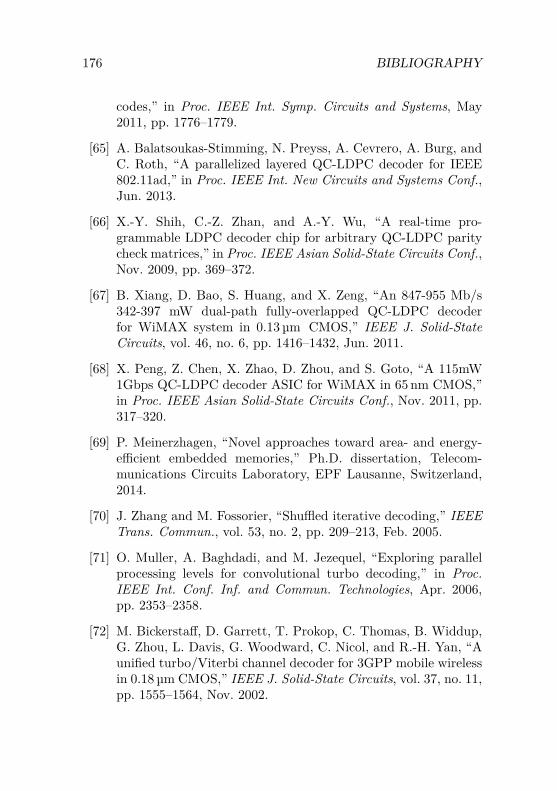
176 BIBLIOGRAPHY
codes,” in Proc. IEEE Int. Symp. Circuits and Systems, May2011, pp. 1776–1779.
[65] A. Balatsoukas-Stimming, N. Preyss, A. Cevrero, A. Burg, andC. Roth, “A parallelized layered QC-LDPC decoder for IEEE802.11ad,” in Proc. IEEE Int. New Circuits and Systems Conf.,Jun. 2013.
[66] X.-Y. Shih, C.-Z. Zhan, and A.-Y. Wu, “A real-time pro-grammable LDPC decoder chip for arbitrary QC-LDPC paritycheck matrices,” in Proc. IEEE Asian Solid-State Circuits Conf.,Nov. 2009, pp. 369–372.
[67] B. Xiang, D. Bao, S. Huang, and X. Zeng, “An 847-955 Mb/s342-397 mW dual-path fully-overlapped QC-LDPC decoderfor WiMAX system in 0.13 µm CMOS,” IEEE J. Solid-StateCircuits, vol. 46, no. 6, pp. 1416–1432, Jun. 2011.
[68] X. Peng, Z. Chen, X. Zhao, D. Zhou, and S. Goto, “A 115mW1Gbps QC-LDPC decoder ASIC for WiMAX in 65 nm CMOS,”in Proc. IEEE Asian Solid-State Circuits Conf., Nov. 2011, pp.317–320.
[69] P. Meinerzhagen, “Novel approaches toward area- and energy-efficient embedded memories,” Ph.D. dissertation, Telecom-munications Circuits Laboratory, EPF Lausanne, Switzerland,2014.
[70] J. Zhang and M. Fossorier, “Shuffled iterative decoding,” IEEETrans. Commun., vol. 53, no. 2, pp. 209–213, Feb. 2005.
[71] O. Muller, A. Baghdadi, and M. Jezequel, “Exploring parallelprocessing levels for convolutional turbo decoding,” in Proc.IEEE Int. Conf. Inf. and Commun. Technologies, Apr. 2006,pp. 2353–2358.
[72] M. Bickerstaff, D. Garrett, T. Prokop, C. Thomas, B. Widdup,G. Zhou, L. Davis, G. Woodward, C. Nicol, and R.-H. Yan, “Aunified turbo/Viterbi channel decoder for 3GPP mobile wirelessin 0.18 µm CMOS,” IEEE J. Solid-State Circuits, vol. 37, no. 11,pp. 1555–1564, Nov. 2002.
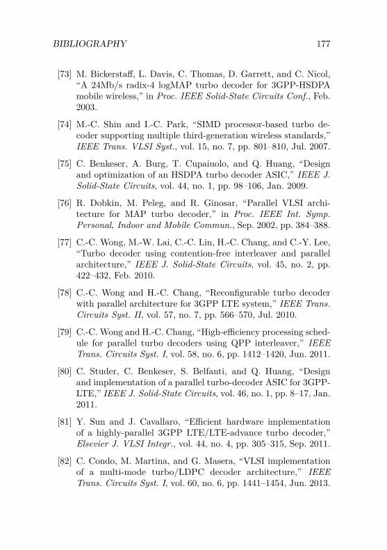
BIBLIOGRAPHY 177
[73] M. Bickerstaff, L. Davis, C. Thomas, D. Garrett, and C. Nicol,“A 24Mb/s radix-4 logMAP turbo decoder for 3GPP-HSDPAmobile wireless,” in Proc. IEEE Solid-State Circuits Conf., Feb.2003.
[74] M.-C. Shin and I.-C. Park, “SIMD processor-based turbo de-coder supporting multiple third-generation wireless standards,”IEEE Trans. VLSI Syst., vol. 15, no. 7, pp. 801–810, Jul. 2007.
[75] C. Benkeser, A. Burg, T. Cupaiuolo, and Q. Huang, “Designand optimization of an HSDPA turbo decoder ASIC,” IEEE J.Solid-State Circuits, vol. 44, no. 1, pp. 98–106, Jan. 2009.
[76] R. Dobkin, M. Peleg, and R. Ginosar, “Parallel VLSI archi-tecture for MAP turbo decoder,” in Proc. IEEE Int. Symp.Personal, Indoor and Mobile Commun., Sep. 2002, pp. 384–388.
[77] C.-C. Wong, M.-W. Lai, C.-C. Lin, H.-C. Chang, and C.-Y. Lee,“Turbo decoder using contention-free interleaver and parallelarchitecture,” IEEE J. Solid-State Circuits, vol. 45, no. 2, pp.422–432, Feb. 2010.
[78] C.-C. Wong and H.-C. Chang, “Reconfigurable turbo decoderwith parallel architecture for 3GPP LTE system,” IEEE Trans.Circuits Syst. II, vol. 57, no. 7, pp. 566–570, Jul. 2010.
[79] C.-C. Wong and H.-C. Chang, “High-efficiency processing sched-ule for parallel turbo decoders using QPP interleaver,” IEEETrans. Circuits Syst. I, vol. 58, no. 6, pp. 1412–1420, Jun. 2011.
[80] C. Studer, C. Benkeser, S. Belfanti, and Q. Huang, “Designand implementation of a parallel turbo-decoder ASIC for 3GPP-LTE,” IEEE J. Solid-State Circuits, vol. 46, no. 1, pp. 8–17, Jan.2011.
[81] Y. Sun and J. Cavallaro, “Efficient hardware implementationof a highly-parallel 3GPP LTE/LTE-advance turbo decoder,”Elsevier J. VLSI Integr., vol. 44, no. 4, pp. 305–315, Sep. 2011.
[82] C. Condo, M. Martina, and G. Masera, “VLSI implementationof a multi-mode turbo/LDPC decoder architecture,” IEEETrans. Circuits Syst. I, vol. 60, no. 6, pp. 1441–1454, Jun. 2013.

178 BIBLIOGRAPHY
[83] T. Ilnseher, F. Kienle, C. Weis, and N. Wehn, “A 2.15GBit/sturbo code decoder for LTE advanced base station applications,”in Proc. Int. Symp. Turbo Codes and Iterative Inf. Processing,Aug. 2012, pp. 21–25.
[84] O. Takeshita, “On maximum contention-free interleavers andpermutation polynomials over integer rings,” IEEE Trans. Inf.Theory, vol. 52, no. 3, pp. 1249–1253, Mar. 2006.
[85] S. Benedetto, D. Divsalar, G. Montorsi, and F. Pollara, “Soft-output decoding algorithms for continuous decoding of parallelconcatenated convolutional codes,” in Proc. IEEE Int. Conf.Commun., Jun. 1996, pp. 112–117.
[86] J. Dielissen and J. Huisken, “State vector reduction for initial-ization of sliding windows MAP,” in Proc. Int. Symp. TurboCodes and Iterative Inf. Processing, Sep. 2000, pp. 387–390.
[87] G. Masera, M. Mazza, G. Piccinini, F. Viglione, and M. Zam-boni, “Architectural strategies for low-power VLSI turbo de-coders,” IEEE Trans. VLSI Syst., vol. 10, no. 3, pp. 279–285,Jun. 2002.
[88] C. Studer, “Iterative MIMO decoding: Algorithms and VLSIimplementation aspects,” Ph.D. dissertation, Integrated Sys-tems Laboratory, ETH Zurich, Switzerland, 2009.
[89] A. Hekstra, “An alternative to metric rescaling in Viterbidecoders,” IEEE Trans. Commun., vol. 37, no. 11, pp. 1220–1222, Nov. 1989.
[90] G. Grani, “VLSI implementation trade-offs of 3G turbo de-coders,” Master’s thesis, Integrated Systems Laboratory, ETHZurich, Switzerland, 2014.
[91] E. Yeo, S. Augsburger, W. Davis, and B. Nikolic, “A 500-mb/ssoft-output Viterbi decoder,” IEEE J. Solid-State Circuits,vol. 38, no. 7, pp. 1234–1241, Jul. 2003.
[92] S. Haene, A. Burg, D. Perels, P. Luethi, N. Felber, andW. Fichtner, “FPGA implementation of Viterbi decoders for
BIBLIOGRAPHY 179
MIMO-BICM,” in Proc. Asilomar Conf. Signals, Systems andComputers, Oct. 2005, pp. 734–738.
[93] G. Feygin and P. Gulak, “Architectural tradeoffs for survivorsequence memory management in Viterbi decoders,” IEEETrans. Commun., vol. 41, no. 3, pp. 425–429, Mar. 1993.
[94] C. Studer, S. Fateh, C. Benkeser, and Q. Huang, “Implemen-tation trade-offs of soft-input soft-output MAP decoders forconvolutional codes,” IEEE Trans. Circuits Syst. I, vol. 59,no. 11, pp. 2774–2783, Nov. 2012.
[95] Channel Coding, 3GPP TS 45.003, Rev. 12.1.0, Jun. 2014.
[96] H. Kroll, S. Zwicky, B. Weber, C. Roth, C. Benkeser, A. Burg,and Q. Huang, “An evolved EDGE PHY ASIC supporting soft-output equalization and Rx diversity,” in Proc. IEEE EuropeanSolid-State Circuits Conf, Sep. 2014, pp. 203–206.
[97] H. Kroll, S. Zwicky, B. Weber, C. Roth, D. Tschopp,C. Benkeser, A. Burg, and Q. Huang, “An evolved GSM/EDGEbaseband ASIC supporting Rx diversity,” IEEE J. Solid-StateCircuits, vol. 50, no. 7, pp. 1690–1701, Apr. 2015.
[98] M. May, T. Ilnseher, N. Wehn, and W. Raab, “A 150Mbit/s3GPP LTE turbo code decoder,” in Proc. Design, AutomationTest in Europe Conf., Mar. 2010, pp. 1420–1425.
[99] Physical Channels and Mapping of Transport Channels ontoPhysical Channels (TDD), 3GPP TS 25.221, Rev. 12.0.0, Sep.2014.
[100] M. Peng, W. Wang, and H.-H. Chen, “TD-SCDMA evolution,”IEEE Veh. Technol. Mag., vol. 5, no. 2, pp. 28–41, Jun. 2010.
[101] High Speed Downlink Packet Access (HSDPA); Overall Descrip-tion; Stage 2, 3GPP TS 25.308, Rev. 12.1.0, Sep. 2014.
[102] P. Frenger, S. Parkvall, and E. Dahlman, “Performance compar-ison of HARQ with Chase combining and incremental redun-dancy for HSDPA,” in Proc. IEEE Veh. Technol. Conf., Oct.2001, pp. 1829–1833.
180 BIBLIOGRAPHY
[103] D. Riegger, “Channel equalization for fast-fading channels inTD-HSPA,” Master’s thesis, Integrated Systems Laboratory,ETH Zurich, Switzerland, 2014.
[104] R. Shao, S. Lin, and M. Fossorier, “Two simple stopping criteriafor turbo decoding,” IEEE Trans. Commun., vol. 47, no. 8, pp.1117–1120, Aug. 1999.
[105] User Equipment (UE) Radio Transmission and Reception(TDD), 3GPP TS 25.102, Rev. 12.0.0, Oct. 2014.
Curriculum Vitae
Christoph Roth was born in Zurich, Switzerland, in 1984. He receivedhis MSc degree in electrical engineering and information technologyfrom ETH Zurich in 2009. In the same year, he joined the IntegratedSystems Laboratory (IIS) at ETH Zurich as a research and teachingassistant.
His research interests include digital signal processing algorithmsand digital VLSI circuits and systems for wireless communication.
181