Embed Size (px)
Citation preview
#istfa2021 | istfaevent.org
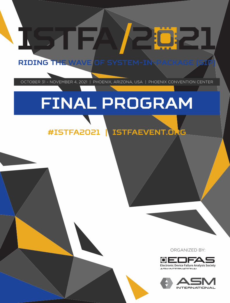
Riding the Wave of System-in-Package (SiP)
ORGANIZED BY:
FINAL PROGRAM
OCTOBER 31 – NOVEMBER 4, 2021 | PHOENIX, ARIZONA, USA | PHOENIX CONVENTION CENTER

Find out more at thermofisher.com/semiconductors
© 2021 Thermo Fisher Scientific Inc. All rights reserved. All trademarks are the property of Thermo Fisher Scientific and its subsidiaries unless otherwise specified. AD0034-08-2021
In our 40 years of working with semiconductor companies, Thermo Fisher Scientific has brought innovative products and workflows to market to help our customers succeed. We continue to accelerate innovation and enhance productivity in every area of semiconductor analysis.
Cloud
Connectivity
Intelligent Edge
Artificial Intelligence
Advancing semiconductor

Technical ProgramTechnical Program: Sunday–Thursday. Dedicated Tutorials on Sunday; integrated Tutorial within the Technical Program on Thursday morning. For more conference details see pages 10–22.
Policy on Cell Phone UsageIn consideration of fellow event attendees and presenters, we request your cooperation in setting cellular phones and/or other electronic devices to ‘silent mode’ in the meeting rooms.
Policy on Audio/Video RecordingsEDFAS and ASM prohibit any unauthorized audio or video recording, or still photography of presentations at ISTFA.
ExhibitionTools of the Trade Tour Monday, November 1, 5:00 p.m. – 6:45 p.m. (Pre-Registration Required)
Exhibit HoursTuesday, November 2, 9:30 a.m. – 6:30 p.m.
Morning Refreshment Break, 9:30 a.m. – 10:10 a.m.Lunch on the Expo Floor, 11:50 a.m. – 12:50 p.m.Afternoon Refreshment Break, 2:05 p.m. – 2:45 p.m.Expo Networking Reception, 5:00 p.m. – 6:30 p.m.
Wednesday, November 3, 9:30 a.m. – 4:00 p.m.Morning Refreshment Break, 10:05 a.m. – 10:30 a.m.Lunch on the Expo Floor, 12:05 p.m. – 1:05 p.m.Expo Dessert Reception, Poster and Video Contest, 1:05 p.m. – 3:05 p.m.
DAY/DATE HOURS LOCATION
Saturday, October 30, 2021 5:00 p.m. – 7:00 p.m. West Halls 1–2 Foyer
Sunday, October 31, 2021 7:00 a.m. – 5:00 p.m. West Halls 1–2 Foyer
Monday, November 1, 2021 7:00 a.m. – 5:00 p.m. West Halls 1–2 Foyer
Tuesday, November 2, 2021 7:30 a.m. – 6:30 p.m. West Halls 1–2 Foyer
Wednesday, November 3, 2021 7:30 a.m. – 5:30 p.m. West Halls 1–2 Foyer
Thursday, November 4, 2021 7:30 a.m. – 1:00 p.m. West Halls 1–2 Foyer
REGISTRATION HOURS
Get ConnectedWant to be hands free at ISTFA? There’s an app for that! Available for Apple and Android devices — visit the iTunes and Google Play Store to download it now.
Download the ISTFA 2021 mobile app to view the most up to date technical program, exhibitor information, networking opportunities, and surveys. Don’t forget to complete the attendee survey on the mobile app and connect with fellow attendees. In addition to the attendee survey, be sure to complete a survey for each tutorial presentation and the Best Paper!
Session Chair & Authors’ Coffee/BriefingPlease join us for coffee, pastries, and a program briefing on the day of your presentation in 106 BC. The room will open at 7:00 a.m. to allow you to meet and network with other participants. The program briefing will begin at 7:30 a.m. to review the program layout, presentation and A/V guidelines, and any final conference details. Poster authors please join us on Wednesday morning. YOUR ATTENDANCE IS VERY IMPORTANT.
Refreshment BreaksSunday – Monday: Meeting Space FoyerTuesday – Wednesday: West Halls 1–2Thursday: Meeting Space Foyer
Career/Resume BoardsStop by Registration to post job openings, find talented people in the industry, or to post a resume on the Career/Resume Board.
Welcome Letter ..................................................................................................................................12021 Organizing Committee ..............................................................................................................2Convention Center Floor Plan ...........................................................................................................6Networking Opportunities .................................................................................................................6Keynote Session .................................................................................................................................8Education Short Courses ...................................................................................................................8Technical Program Schedule ...........................................................................................................10Show Directory .................................................................................................................................25Exhibitor List .....................................................................................................................................26Exhibit Hall Floor Plan .....................................................................................................................27Tools of the Trade Tour ....................................................................................................................29Company Descriptions .....................................................................................................................33Product/Services Index ....................................................................................................................43
TABLE OF CONTENTS
#ISTFA2021
IST
FA
20
21
FIN
AL
PR
OG
RA
M
WELCOME
After a very long year and a half of lockdown, remote work, and video conferencing due to the COVID-19 pandemic, we are finally gathering here for the 47th International Symposium for Testing and Failure Analysis. Welcome to ISTFA 2021!
The theme this year is be “Riding the Wave of System-in-Package (SiP)”. In the 21st century, the electronic market will be driven by consumers with demands of immediate entertainment, fast access to information, and communications anywhere in a personalized fashion and at affordable prices. The new challenge is not how many transistors can be built on a single chip, as in SoC (System-on-Chip), but rather how to integrate diverse circuits together predictably, harmoniously, and cost effectively. Instead of getting twice the transistors for the same cost as Moore’s Law predicted in the past 50 years, the goal of SiP is to obtain the same number of transistors for half the cost within less than half the time to market.
To further understand the roadmap from advanced packaging for heterogeneous integration to future SiP development, our keynote speaker will be Dr. Ravi Mahajan, Intel Fellow and Lead Architect for Packaging Technology Architecture, Assembly & Test Technology. His talk will be centering on “Advanced Packaging for Heterogeneous Integration”. The Panel Discussion will expand upon the keynote speech by focusing on “Overcoming the Challenges in System-in-Package Failure Analysis.” Discussion points will include SiP fault isolation and failure analysis gaps and challenges, SiP in Advanced Driver-Assistance Systems (ADAS), Electrostatic Discharge (ESD) in SiP, and Wafer Level Chip Scale Package (WLCSP) for SiP devices. Distinguished field experts are invited to be on the panel to share their viewpoints and solutions based on their broad work experiences and diverse backgrounds, hopefully inspiring an engaged conversation among the panelists and the audience.
There is no doubt that the core of ISTFA is the technical program, this year we have 18 technical oral presentations and poster sessions with more than 70 technical papers. We also have three new sessions featured with SiP, 3D packaging, and AI topics. Due to current travel restrictions, particularly for the international attendees, more than 20 papers will be presented through pre-recorded video presentations. For the tutorial program, we have 18 Tutorial presentations and 5 Education Short Courses. The majority of tutorial presentations are on Sunday, October 31, in three tracks, except for two tutorials, which will be presented during the technical program on Thursday along with the relevant technical papers. The education short courses, which will provide much more detailed learning on selected topics, will start on Saturday, October 30, before the main conference events kick-off.
Each year at ISTFA, the most participated events are the User Group discussions. This year, it’s especially important to have face-to-face interaction with our colleagues from the industry as we missed it so much throughout this pandemic. It’s an open forum filled with mini-presentations, floor-initiated topics, and a robust interchange of ideas. Come with your questions, complaints, suggestions, tips and tricks, and the like. Share what you know, enquire about something new, challenge the status quo. There will be four sessions this year covering FIB, Sample Preparation, Nanoprobing and Contactless Probing, and 3D System-on-Package Failure Analysis.
The ISTFA Expo is another reason for many people to attend the ISTFA conference in person. It’s the perfect place for vendors to showcase the latest development in their tools and techniques; for the tool users, it creates an ideal environment to meet their suppliers and other users all at one time and to gather information about next generation tools on your wish list. We are happy to announce that more than 50 exhibitors will be at the expo with more than 60 booths this year as we start to emerge from this ongoing pandemic. We also have six vendors signed up for the highly anticipated Tools of the Trade Tour on Monday evening.
This year, the Roadmap committee has integrated Roadmap elements into both the Panel Discussion and User Group sessions so our entire FA community can start to form dedicated discussions around developing a clear FA Technology Roadmap for the years to come. Also, following its successful introduction in the past two years, Women in Electronics Failure Analysis (WEFA) will hold another panel discussion this year.
After a successful online ISTFA Workshop in 2020, we are looking forward to seeing you in person at ISTFA this year where we can reconnect with each other to advance our knowledge learning, information sharing, and professional growth. Many new safety protocols will be in place for your comfort and protection throughout the conference. On behalf of the ISTFA organizing committee, I welcome you to ISTFA 2021.
Susan Li, Infineon TechnologiesISTFA 2021 General Chair
2IS
TFA
20
21
FIN
AL
PR
OG
RA
MISTFA 2021 ORGANIZING COMMITTEE
General ChairSusan LiInfineon Technologies
Vice General ChairZhigang SongIBM
Technical Program ChairFrank AltmannFraunhofer IMWS
Expo ChairBecki WattSiemens
Committee Members
Tutorial ChairChristian SchmidtNVIDIA
Tutorial Vice-ChairKristofor DicksonNXP
Panel Chair Yan LiIntel
Panel Vice-ChairRandal MulderSilicon Labs
Exposition Vice-Chair/Video ChairRose RingHRL
FA Roadmap ChairKeith SerrelsNXP
FA Roadmap Vice-ChairVinod NarangAdvanced Micro Devices
User Group ChairAnita MadanIndependent Consultant
User Group Vice-ChairDaminda DahanayakaGLOBALFOUNDRIES
AV ChairRenee ParenteAMD
AV Vice-Chair/ Local Arrangements Chair Ted KolasaNorthrop Grumman
International ChairSzuhuat GohGLOBALFOUNDRIES
International Vice-ChairVinod NarangAdvanced Micro Devices
3IS
TFA
20
21 F
INA
L P
RO
GR
AM
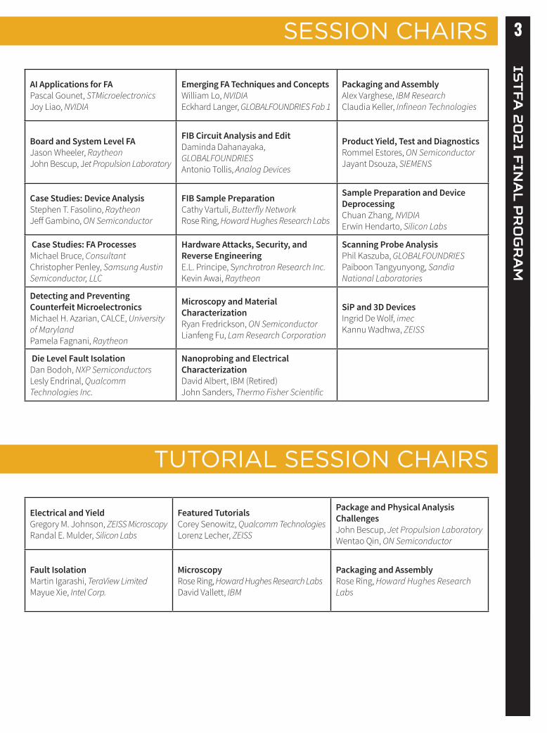
SESSION CHAIRS
AI Applications for FAPascal Gounet, STMicroelectronicsJoy Liao, NVIDIA
Emerging FA Techniques and ConceptsWilliam Lo, NVIDIAEckhard Langer, GLOBALFOUNDRIES Fab 1
Packaging and AssemblyAlex Varghese, IBM ResearchClaudia Keller, Infineon Technologies
Board and System Level FAJason Wheeler, RaytheonJohn Bescup, Jet Propulsion Laboratory
FIB Circuit Analysis and EditDaminda Dahanayaka, GLOBALFOUNDRIESAntonio Tollis, Analog Devices
Product Yield, Test and DiagnosticsRommel Estores, ON SemiconductorJayant Dsouza, SIEMENS
Case Studies: Device AnalysisStephen T. Fasolino, RaytheonJeff Gambino, ON Semiconductor
FIB Sample PreparationCathy Vartuli, Butterfly NetworkRose Ring, Howard Hughes Research Labs
Sample Preparation and Device DeprocessingChuan Zhang, NVIDIAErwin Hendarto, Silicon Labs
Case Studies: FA ProcessesMichael Bruce, ConsultantChristopher Penley, Samsung Austin Semiconductor, LLC
Hardware Attacks, Security, and Reverse EngineeringE.L. Principe, Synchrotron Research Inc.Kevin Awai, Raytheon
Scanning Probe AnalysisPhil Kaszuba, GLOBALFOUNDRIESPaiboon Tangyunyong, Sandia National Laboratories
Detecting and Preventing Counterfeit MicroelectronicsMichael H. Azarian, CALCE, University of MarylandPamela Fagnani, Raytheon
Microscopy and Material CharacterizationRyan Fredrickson, ON SemiconductorLianfeng Fu, Lam Research Corporation
SiP and 3D DevicesIngrid De Wolf, imecKannu Wadhwa, ZEISS
Die Level Fault IsolationDan Bodoh, NXP SemiconductorsLesly Endrinal, Qualcomm Technologies Inc.
Nanoprobing and Electrical CharacterizationDavid Albert, IBM (Retired)John Sanders, Thermo Fisher Scientific
Electrical and YieldGregory M. Johnson, ZEISS MicroscopyRandal E. Mulder, Silicon Labs
Featured TutorialsCorey Senowitz, Qualcomm TechnologiesLorenz Lecher, ZEISS
Package and Physical Analysis ChallengesJohn Bescup, Jet Propulsion Laboratory Wentao Qin, ON Semiconductor
Fault IsolationMartin Igarashi, TeraView LimitedMayue Xie, Intel Corp.
MicroscopyRose Ring, Howard Hughes Research LabsDavid Vallett, IBM
Packaging and AssemblyRose Ring, Howard Hughes Research Labs
TUTORIAL SESSION CHAIRS
4IS
TFA
20
21
FIN
AL
PR
OG
RA
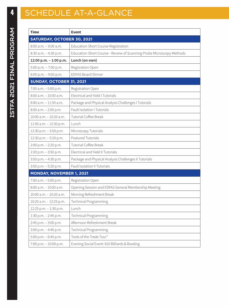
MSCHEDULE AT-A-GLANCE
Time Event
SATURDAY, OCTOBER 30, 2021
8:00 a.m. – 9:00 a.m. Education Short Course Registration
8:30 a.m. – 4:30 p.m. Education Short Course - Review of Scanning Probe Microscopy Methods
12:00 p.m. – 1:00 p.m. Lunch (on own)
5:00 p.m. – 7:00 p.m. Regisration Open
6:00 p.m. – 9:00 p.m. EDFAS Board Dinner
SUNDAY, OCTOBER 31, 2021
7:00 a.m. – 5:00 p.m. Registration Open
8:00 a.m. – 10:00 a.m. Electrical and Yield I Tutorials
8:00 a.m. – 11:50 a.m. Package and Physical Analysis Challenges I Tutorials
8:00 a.m. – 2:00 p.m. Fault Isolation I Tutorials
10:00 a.m. – 10:20 a.m. Tutorial Coffee Break
11:50 a.m. – 12:30 p.m. Lunch
12:30 p.m. – 3:50 p.m. Microscopy Tutorials
12:30 p.m. – 5:20 p.m. Featured Tutorials
2:00 p.m. – 2:20 p.m. Tutorial Coffee Break
2:20 p.m. – 3:50 p.m. Electrical and Yield II Tutorials
3:50 p.m. – 4:30 p.m. Package and Physical Analysis Challenges II Tutorials
3:50 p.m. – 5:20 p.m. Fault Isolation II Tutorials
MONDAY, NOVEMBER 1, 2021
7:00 a.m. – 5:00 p.m. Registration Open
8:00 a.m. – 10:00 a.m. Opening Session and EDFAS General Membership Meeting
10:00 a.m. – 10:20 a.m. Morning Refreshment Break
10:20 a.m. – 12:25 p.m. Technical Programming
12:25 p.m. – 1:30 p.m. Lunch
1:30 p.m. – 2:45 p.m. Technical Programming
2:45 p.m. – 3:00 p.m. Afternoon Refreshment Break
3:00 p.m. – 4:40 p.m. Technical Programming
5:00 p.m. – 6:45 p.m. Tools of the Trade Tour*
7:00 p.m. – 10:00 p.m. Evening Social Event: 810 Billiards & Bowling
5IS
TFA
20
21 F
INA
L P
RO
GR
AM
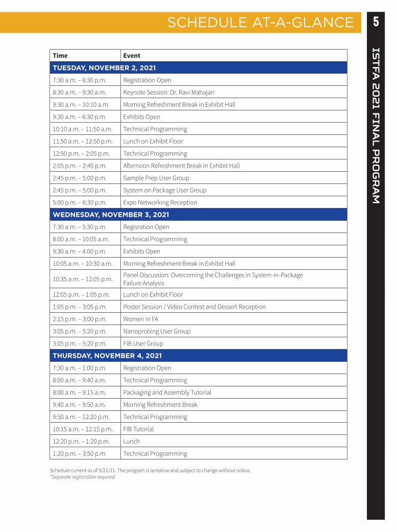
SCHEDULE AT-A-GLANCE
Schedule current as of 9/21/21. The program is tentative and subject to change without notice.*Separate registration required
Time Event
TUESDAY, NOVEMBER 2, 2021
7:30 a.m. – 6:30 p.m. Registration Open
8:30 a.m. – 9:30 a.m. Keynote Session: Dr. Ravi Mahajan
9:30 a.m. – 10:10 a.m. Morning Refreshment Break in Exhibit Hall
9:30 a.m. – 6:30 p.m. Exhibits Open
10:10 a.m. – 11:50 a.m. Technical Programming
11:50 a.m. – 12:50 p.m. Lunch on Exhibit Floor
12:50 p.m. – 2:05 p.m. Technical Programming
2:05 p.m. – 2:45 p.m. Afternoon Refreshment Break in Exhibit Hall
2:45 p.m. – 5:00 p.m. Sample Prep User Group
2:45 p.m. – 5:00 p.m. System on Package User Group
5:00 p.m. – 6:30 p.m. Expo Networking Reception
WEDNESDAY, NOVEMBER 3, 2021
7:30 a.m. – 5:30 p.m. Regisration Open
8:00 a.m. – 10:05 a.m. Technical Programming
9:30 a.m. – 4:00 p.m. Exhibits Open
10:05 a.m. – 10:30 a.m. Morning Refreshment Break in Exhibit Hall
10:35 a.m. – 12:05 p.m. Panel Discussion: Overcoming the Challenges in System-in-Package Failure Analysis
12:05 p.m. – 1:05 p.m. Lunch on Exhibit Floor
1:05 p.m. – 3:05 p.m. Poster Session / Video Contest and Dessert Reception
2:15 p.m. – 3:00 p.m. Women in FA
3:05 p.m. – 5:20 p.m. Nanoprobing User Group
3:05 p.m. – 5:20 p.m. FIB User Group
THURSDAY, NOVEMBER 4, 2021
7:30 a.m. – 1:00 p.m. Registration Open
8:00 a.m. – 9:40 a.m. Technical Programming
8:00 a.m. – 9:15 a.m. Packaging and Assembly Tutorial
9:40 a.m. – 9:50 a.m. Morning Refreshment Break
9:50 a.m. – 12:20 p.m. Technical Programming
10:15 a.m. – 12:15 p.m. FIB Tutorial
12:20 p.m. – 1:20 p.m. Lunch
1:20 p.m. – 3:50 p.m. Technical Programming
6IS
TFA
20
21
FIN
AL
PR
OG
RA
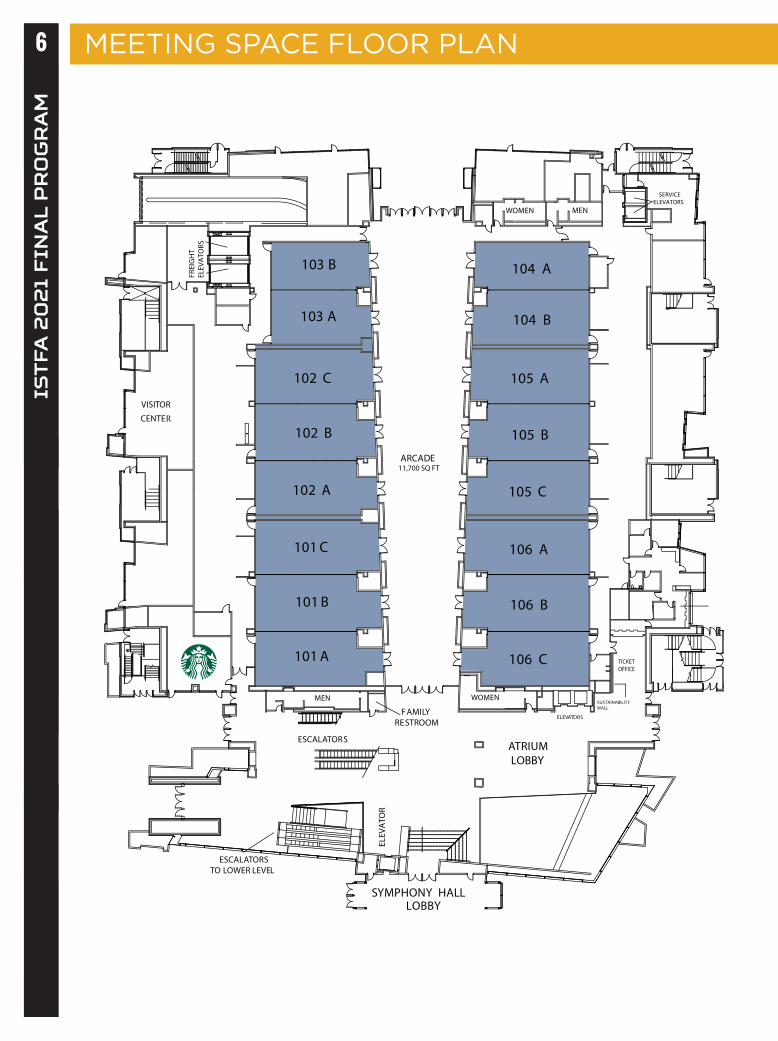
MMEETING SPACE FLOOR PLAN
103 B
103 A
102 C
102 B
102 A
101 C
101 B
101 A
SECO
ND
STR
EET
THIR
D S
TREE
T
SYMPHONY HALLLOBBY
ATRIUMLOBBY
ARCADE11,700 SQ FT
104 A
104 B
105 A
105 B
105 C
106 A
106 B
106 C
N
MEN WOMEN
WEST GARAGEENTRANCE/EXIT
FREI
GH
TEL
EVA
TORS
MENWOMEN
ESCALATORSTO LOWER LEVEL
ESCALATORS
F AMILYRESTROOM
ELEV
ATO
R
ELEVATORS
TICKETOFFICE
VISITOR
CENTER
MEDIABOX
MEDIABOX
SUSTAINABILITYWALL
STREET ACCESSTO EXTERIORTICKET OFFICE
SERVICEELEVATORS
W E S T B U I L D I N G | 1 0 0 L E V E L
M O N R O E S T R E E T
SE
CO
ND
S
TR
EE
T
TH
IR
D
ST
RE
ET
7IS
TFA
20
21 F
INA
L P
RO
GR
AM
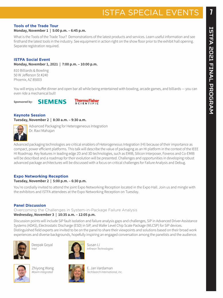
ISTFA SPECIAL EVENTSTools of the Trade TourMonday, November 1 | 5:00 p.m. – 6:45 p.m.
What is the Tools of the Trade Tour? Demonstrations of the latest products and services. Learn useful information and see firsthand the latest tools in the industry. See equipment in action right on the show floor prior to the exhibit hall opening. Separate registration required.
ISTFA Social EventMonday, November 1, 2021 | 7:00 p.m. – 10:00 p.m.
810 Billiards & Bowling50 W Jefferson St #240Phoenix, AZ 85003
You will enjoy a buffet dinner and open bar all while being entertained with bowling, arcade games, and billiards — you can even ride a mechanical bull!
Sponsored by:
Keynote SessionTuesday, November 2 | 8:30 a.m. – 9:30 a.m.
Advanced Packaging for Heterogeneous Integration Dr. Ravi Mahajan
Advanced packaging technologies are critical enablers of Heterogeneous Integration (HI) because of their importance as compact, power efficient platforms. This talk will describe the value of packaging as an HI platform in the context of the IEEE HI Roadmap. Key features in leading edge 2D and 3D technologies, such as EMIB, Silicon Interposer, Foveros and Co-EMIB will be described and a roadmap for their evolution will be presented. Challenges and opportunities in developing robust advanced package architectures will be discussed with a focus on critical challenges for Failure Analysis and Debug.
Expo Networking Reception Tuesday, November 2 | 5:00 p.m. – 6:30 p.m.
You’re cordially invited to attend the joint Expo Networking Reception located in the Expo Hall. Join us and mingle with the exhibitors and ISTFA attendees at the Expo Networking Reception on Tuesday.
Panel DiscussionOvercoming the Challenges in System-in-Package Failure AnalysisWednesday, November 3 | 10:35 a.m. – 12:05 p.m.
Discussion points will include SiP fault isolation and failure analysis gaps and challenges, SiP in Advanced Driver-Assistance Systems (ADAS), Electrostatic Discharge (ESD) in SiP, and Wafer Level Chip Scale Package (WLCSP) for SiP devices. Distinguished field experts are invited to be on the panel to share their viewpoints and solutions based on their broad work experiences and diverse backgrounds, hopefully inspiring an engaged conversation among the panelists and the audience.
Deepak GoyalIntel
Zhiyong WangMaxim Integrated
Susan LiInfineon Technologies
E. Jan VardamanTechSearch International, Inc.
8IS
TFA
20
21
FIN
AL
PR
OG
RA
MISTFA SPECIAL EVENTS
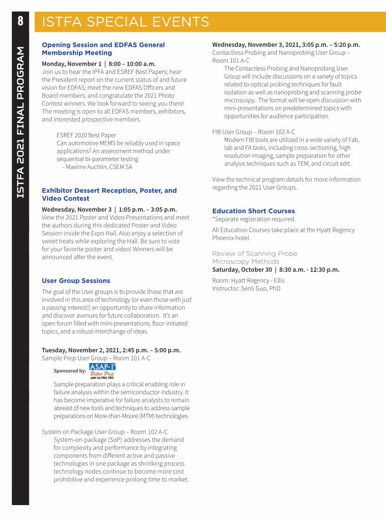
Wednesday, November 3, 2021, 3:05 p.m. – 5:20 p.m.Contactless Probing and Nanoprobing User Group – Room 101 A-C
The Contactless Probing and Nanoprobing User Group will include discussions on a variety of topics related to optical probing techniques for fault isolation as well as nanoprobing and scanning probe microscopy. The format will be open discussion with mini-presentations on predetermined topics with opportunities for audience participation.
FIB User Group – Room 102 A-CModern FIB tools are utilized in a wide variety of Fab, lab and FA tasks, including cross-sectioning, high resolution imaging, sample preparation for other analysis techniques such as TEM, and circuit edit.
View the technical program details for more information regarding the 2021 User Groups.
Education Short Courses*Separate registration required.
All Education Courses take place at the Hyatt Regency Phoenix hotel.
Review of Scanning Probe Microscopy MethodsSaturday, October 30 | 8:30 a.m. - 12:30 p.m.
Room: Hyatt Regency - EllisInstructor: Senli Guo, PhD
Opening Session and EDFAS General Membership Meeting
Monday, November 1 | 8:00 – 10:00 a.m.Join us to hear the IPFA and ESREF Best Papers; hear the President report on the current status of and future vision for EDFAS; meet the new EDFAS Officers and Board members; and congratulate the 2021 Photo Contest winners. We look forward to seeing you there! The meeting is open to all EDFAS members, exhibitors, and interested prospective members.
ESREF 2020 Best PaperCan automotive MEMS be reliably used in space applications? An assessment method under sequential bi-parameter testing
- Maxime Auchlin, CSEM SA
Exhibitor Dessert Reception, Poster, and Video Contest
Wednesday, November 3 | 1:05 p.m. – 3:05 p.m.View the 2021 Poster and Video Presentations and meet the authors during this dedicated Poster and Video Session inside the Expo Hall. Also enjoy a selection of sweet treats while exploring the Hall. Be sure to vote for your favorite poster and video! Winners will be announced after the event.
User Group Sessions
The goal of the User groups is to provide those that are involved in this area of technology (or even those with just a passing interest!) an opportunity to share information and discover avenues for future collaboration. It’s an open forum filled with mini-presentations, floor-initiated topics, and a robust interchange of ideas.
Tuesday, November 2, 2021, 2:45 p.m. – 5:00 p.m.Sample Prep User Group – Room 101 A-C
Sponsored by:
Sample preparation plays a critical enabling role in failure analysis within the semiconductor industry. It has become imperative for failure analysts to remain abreast of new tools and techniques to address sample preparations on More-than-Moore (MTM) technologies.
System on Package User Group – Room 102 A-CSystem-on-package (SoP) addresses the demand for complexity and performance by integrating components from different active and passive technologies in one package as shrinking process technology nodes continue to become more cost prohibitive and experience prolong time to market.
imatevent.org
CO-LOCATED WITH:
NORTH AMERICAN COLD SPRAY CONFERENCE 2022
ORGANIZED BY:
2022
INTERNATIONAL MATERIALS,APPLICATIONS & TECHNOLOGIES
SEPTEMBER 12-15, 2022 | ERNEST N. MORIAL CONVENTION CENTER NEW ORLEANS, LA
STRONGER. TOGETHER.
IMAT is ASM’s Annual Meeting. A diverse group of materials experts, including the ASM Programming
Committees, AeroMat Committee, and all six of ASM’s A� iliate Societies, are heavily involved in
building the technical symposiums, which will have a strong focus on application-oriented, real-world
technologies that can be put to use today.
10IS
TFA
20
21
FIN
AL
PR
OG
RA
MTECHNICAL PROGRAM
SUNDAY, OCTOBER 31, 2021
FOR THE MOST ACCURATE AND UP TO DATE SCHEDULE, PLEASE REFER TO THE ISTFA MOBILE APP.
ELECTRICAL AND YIELD TUTORIALS I 8:00 a.m. – 10:00 a.m. Meeting Room: 104 AB
Session Chairs: Mr. Gregory Johnson ZEISS Microscopy Poughkeepsie, NY USA
Mr. Randal E. Mulder Silicon Labs Austin, TX USA
8:00 a.m.The Fundamentals of Nanoprobe Analysis: Mr. Randal E. Mulder, Device Analysis Lab, Silicon Labs, Austin, TX
9:00 a.m.Machine learning based data and signal analysis methods for the application in failure analysis: Mr. Michael Kögel1, Dr. Sebastian Brand1 and Mr. Frank Altmann2, 1Center for Applied Microstructure Diagnostics (CAM), Fraunhofer Institute for Microstructure of Materials and Systems IMWS, Halle, Germany, 2Electronic Materials and Components, Fraunhofer Institute for Microstructure of Materials and Systems IMWS, Halle, Germany
FAULT ISOLATION TUTORIALS I 8:00 a.m. – 2:00 p.m. Meeting Room: 105 AB
Session Chairs: Mr. Martin Igarashi TeraView Limited Cambridge, United Kingdom
Dr. Mayue Xie Intel corp Chandler, AZ USA
8:00 a.m.Defect localization by Lock-In-Thermography: Dr. Sebastian Brand, Fraunhofer Institute for Microstructure of Materials and Systems, Halle, Germany
9:00 a.m.Photonic Localization Techniques: Prof. Christian Boit, Semiconductor Devices, Technische Universitaet Berlin, Berlin, Germany
10:00 a.m. Morning Refreshment Break
10:20 a.m.LADA and SDL: Powerful Techniques for Marginal Failures: Mr. Dan Bodoh and Mr. Kent Erington, Failure Analysis Collaboration and Development, NXP Semiconductors, Austin, TX
11:50 a.m. Lunch
12:30 p.m.FA Technique Selection for Front End Defect Localization in Bulk Semiconductor (Si) FA: Mr. Gregory Johnson, Electronics, ZEISS Microscopy, Poughkeepsie, NY
PACKAGE AND PHYSICAL ANALYSIS CHALLENGES TUTORIALS I 8:00 a.m. – 11:50 a.m. Meeting Room: 103 AB
Session Chairs: Mr. John Bescup Jet Propulsion Laboratory Pasadena, CA USA
Dr. Wentao Qin ON Semiconductor Phoenix, AZ USA
8:00 a.m.Chip Scale Packaging and Its Failure Analysis Challenges: Ms. Susan Li, Failure Analysis Engineering, Infineon Technologies, San Jose, CA
9:00 a.m.Electromigration Analysis located between the internal layers of a Printed Circuit Board: Dr. Miguel Angel Neri, Doctorate on Materials Engineering, Metallurgy and Structural Integrity, Advanced materiales Research Center, S. C., Chihuahua, CI, Mexico
10:00 a.m. Morning Refreshment Break
10:20 a.m.Package Level Fault Isolation: Dr. Lihong Cao, ASE US Inc, Sunnyvale, CA
11IS
TFA
20
21 F
INA
L P
RO
GR
AM
TECHNICAL PROGRAMFEATURED TUTORIALS12:30 p.m. – 5:20 p.m. Meeting Room: 104 AB
Session Chairs: Mr. Lorenz Lechner Zeiss Pleasanton, CA USA
Mr. Corey Senowitz Qualcomm Technologies Inc. San Diego, CA USA
12:30 p.m.
Focused Ion Beam (FIB) for Microchip Circuit Edit and Fault Isolation : Mr. Steven B. Herschbein1, Dr. Shida Tan2, Mr. Richard H. Livengood2 and Mr. Michael Wong3, 1Consultant, Hopewell Junction, NY, 2Physical Debug Development Lab, Intel Corporation, Santa Clara, CA, 3Electrical Failure Analysis, Thermo Fisher Scientific, Fremont, CA
2:00 p.m. Afternoon Refreshment Break
2:20 p.m.EOS/ESD Failure Mechanisms and Design Solutions: Dr. Steven Voldman, Steven H. Voldman LLC, Lake Placid, NY
3:50 p.m.3D device/package fault isolation and failure analysis: Prof. Ingrid De Wolf and Dr. Kristof J.P. Jacobs, imec, Leuven, Belgium
MICROSCOPY TUTORIALS 12:30 p.m. – 3:50 p.m. Meeting Room: 103 AB
Session Chairs: Ms. Rose Ring Howard Hughes Research Labs, LLC Malibu, CA USA
Mr. Dave Vallett IBM Burlington, VT USA
12:30 p.m.Scanning Transmission Electron Microscopy in a Scanning Electron Microscope: From Basic to Quantitative Imaging and Diffraction: Dr. Jason Holm, Materials Measurement Laboratory, National Institute of Standards and Technology, Boulder, CO
2:00 p.m. Afternoon Refreshment Break
2:20 p.m.Basics and current aspects of scanning electron microscopy: Dr. Heiko Stegmann, Carl Zeiss Microscopy GmbH, Oberkochen, Germany
ELECTRICAL AND YIELD TUTORIAL II 2:20 p.m. – 3:50 p.m. Meeting Room: 105 AB
Session Chairs: Mr. Gregory Johnson ZEISS Microscopy Poughkeepsie, NY USA
Mr. Randal E. Mulder Silicon Labs Austin, TX USA
2:20 p.m.Yield Basics for Failure Analysts: Mr. David Albert1 and Mr. Tracy Myers2, 1IBM (Retired), Hopewell Junction, NY, 2Corporate R&D, MTS, ON Semiconductor, Gresham, OR
FAULT ISOLATION TUTORIAL II 3:50 p.m. – 5:20 p.m. Meeting Room: 103 AB
Session Chairs: Mr. Martin Igarashi TeraView Limited Cambridge, United Kingdom
Dr. Mayue Xie Intel corp Chandler, AZ USA
3:50 p.m.Flip-Chip and Backside Techniques: Dr. Edward I. Cole Jr., FASM, National Security Programs, Sandia National Laboratories, Albuquerque, NM
PACKAGE AND PHYSICAL ANALYSIS CHALLENGES TUTORIAL II 3:50 p.m. – 5:30 p.m. Meeting Room: 105 AB
Session Chairs: Mr. John Bescup Jet Propulsion Laboratory Pasadena, CA USA
Dr. Wentao Qin ON Semiconductor Phoenix, AZ USA
3:50 p.m.Failure analysis for hardware security: Dr. Navid Asadi, University of Florida, Gainesville, FL
13IS
TFA
20
21 F
INA
L P
RO
GR
AM
TECHNICAL PROGRAM
MONDAY, NOVEMBER 1, 2021
EMERGING FA TECHNIQUES AND CONCEPTS 10:20 a.m. – 12:25 p.m. Meeting Room: West 301 A
Session Chairs: Dr. William Lo NVIDIA Corporation Santa Clara, CA USA
Dr. Eckhard Langer Globalfoundries Fab 1 Dresden, Germany
10:20 a.m.INVITED: Why Chiplets?: Ms. Jan Vardaman, Tech Search Inc., Austin, TX
11:00 a.m.Vector Magnetic Current Imaging of an 8 nm Process Node Chip and 3D Current Distributions Using the Quantum Diamond Microscope: Dr. Sean M. Oliver1,2, Dr. Dmitro J. Martynowych1, Dr. Matthew J. Turner2,3,4, Dr. David A. Hopper1, Prof. Ronald L. Walsworth2,3,4, and Dr. Edlyn V. Levine1,5, 1The MITRE Corporation, McLean, VA, 2Quantum Technology Center, University of Maryland, College Park, MD, 3Department of Electical and Computer Engineering, University of Maryland, College Park, MD, 4Department of Physics, University of Maryland, College Park, MD, 5Department of Physics, Harvard University, Cambridge, MA
11:25 a.m.Heterogeneous Industry Collaboration and System Navigation for Advanced Packages: Mr. Arpan Bhattacherjee1, Mr. Anand Shankar2, Mr. Arshdeep Singh3 and Ms. Mehak Singla4, 1Silicon Engineering Group, Synopsys Inc, Mountain View, CA, 2Silicon Engineering Group, Synopsys Inc., Mira Road, Thane, India, 3Silicon Engineering Group, Synopsys Inc., Jammu, Jammu and Kashmir, India, 4Silicon Engineering Group, Synopsys GmbH, Aschheim, Germany
11:50 a.m.Photon Emission Microscopy of HfO2 ReRAM Cells: Dr. Franco Stellari1, N/A Ernest wu2, Dr. Takashi Ando3, Dr. Martin Frank3 and Dr. Peilin Song4, 1IBM, Yorktown Heights, NY, 2IBM Research, Essex Junction, VT, 3IBM Research, Yorktown Heights, NY, 4Circuit Test and Diagnostics Technology, IBM T.J. Watson Research Center, Yorktown Heights, NY
DETECTING AND PREVENTING COUNTERFEIT MICROELECTRONICS 1:30 p.m. – 2:45 p.m. Meeting Room: 104 AB
Session Chairs: Michael Azarian CALCE, University of Maryland College Park, MD USA
Ms. Pamela C. Fagnani Raytheon El Segundo, CA USA
1:30 p.m.Scanning Acoustic Microscopy Package Fingerprint Extraction for Integrate Circuit Hardware Assurance: Mr. Daniel Johnson1, Mr. Po Wei Hsu2, Mr. Chengjie Xi3 and Dr. Navid Asadizanjani1, 1University of Florida, Gainesville, FL, 2FICS, University of Florida, Gainesville, FL, 3Electrical and Computer Engineering, Florida Institute for Cybersecurity, University of Florida, Gainesville, FL
1:55 p.m.EC-SEG: Electronic Component Segmentation for PCB Assurance and Counterfeit Avoidance: Mr. Mukhil Azhagan Mallaiyan Sathiaseelan, Mr. Manoj Yasaswi Vutukuru, Mr. Sudarshan Agrawal and Dr. Navid Asadizanjani, Electrical and Computer Engineering, University of Florida, Gainesville, FL
SCANNING PROBE ANALYSIS 1:30 p.m. – 2:45 p.m. Meeting Room: 105 AB
Session Chairs: Mr. Phil Kaszuba Globalfoundries Essex Junction, VT USA
Pai Tangyunyong Sandia National Laboratories Albuquerque, NM USA
1:30 p.m.Advances in Scanning Microwave Impedance Microscopy: Dr. Ravi Chandra Chintala, Mr. Nicholas Antoniou and Dr. Yongliang Yang, Primenano Inc., Santa Clara, CA
1:55 p.m.Simultaneous interface defect density and differential capacitance imaging by time-resolved scanning nonlinear dielectric microscopy: Prof. Kohei Yamasue and Prof. Yasuo Cho, Research Institute of Electrical Communication, Tohoku University, Sendai, Japan
14IS
TFA
20
21
FIN
AL
PR
OG
RA
M
DIE LEVEL FAULT ISOLATION 3:00 p.m. – 4:30 p.m. Meeting Room: 105 AB
Session Chairs: Mr. Dan Bodoh NXP Semiconductors Austin, TX USA
Ms. Lesly Endrinal Qualcomm Technologies Inc. San Diego, CA USA
3:00 p.m.Failure Localization Techniques for 7nm & 16nm Process Nodes in Monolithic & 2.5D SSIT Package Technology Using OBIRCH, LVP and Advance Die Thinning Method: Mr. Daniel Nuez1, Mr. Phoumra Tan2, Mrs. Daisy Lu1, Mr. Benhai Zhang1, Mr. Tom Harper3, Mr. Josh Miller3, Mr. Mark Lynaugh3, Dr. Michael DiBattista3 and Mr. Scott Silverman3, 1QNG, Xilinx, San Jose, CA, 2Global Operations and Quality, Xilinx, Inc, San Jose, CA, 3Varioscale, San Marcos, CA
3:25 p.m.Measurement of the Internal Operation of DRAM WL and BL Charge Sharing by utilizing LVP/LVI Analysis Technology: Mr. Yongwon Kim, SK Hynix, Icheon, Korea, Republic of (South)
3:50 p.m.Pushing Failure Mode Stimulus to Overcome the Limitation/Boundaries of Soft Defect Localization Tools: Mr. Allan Norico1 and Mr. Rommel Estores2, 1FA, ON Semiconductor, Oudenaarde, Belgium, 2Quality, ON Semiconductor, Oudenaarde, Belgium
SIP AND 3D DEVICES 3:00 p.m. – 4:30 p.m. Meeting Room: 104 AB
Session Chairs: Prof. Ingrid De Wolf imec Leuven, Belgium
Ms. Kannu Wadhwa ZEISS Dublin, CA USA
3:00 p.m. (V) INVITED: Back-side Power Delivery Network: Innovative scaling booster for 3D heterogeneous integrationDr. Anne Jourdain, Imec, Leuven, Belgium
3:40 p.m.Fault isolation approaches for nanoscale TSV interconnects in 3D heterogenous integration: Dr. Kristof J.P. Jacobs1, Dr. Anne Jourdain2, Prof. Ingrid De Wolf1 and Dr. Eric Beyne2, 1imec, Leuven, Belgium, 2Imec, Leuven, Belgium
4:05 p.m.Quantitative evaluation of bonded silicon wafer by Scanning Acoustic Tomography: Mr. Koutaro Kikukawa1, Mr. Natsuki Sugaya1, Mr. Yoshihiro Tomita2 and Dr. Shigeru Ohno1, 1Hitachi Power Solutions Co., Ltd., Hitachinaka, Ibaraki, Japan, 2Intel K.K., Chiyoda, Tokyo, Japan
CASE STUDIES: FA PROCESSES 4:15 p.m. – 4:40 p.m. Meeting Room: 103 AB
Session Chairs: Dr. Mike Bruce Independant TX USA
Mr. Christopher Penley Samsung Austin Semiconductor, LLC Austin, TX USA
4:15 p.m.High Aspect Ratio, Vertical Bipolar Junction Transistor NPN Device Fault Isolation & Analysis Techniques: Mr. Kevin A. Distelhurst, BS/MS Electrical Engineering and Mr. Daniel A. Bader, GLOBALFOUNDRIES, Essex Jct., VT
TECHNICAL PROGRAM
16IS
TFA
20
21
FIN
AL
PR
OG
RA
M
KEYNOTE SESSION: DR. RAVI MAHAJAN 8:30 a.m. – 9:30 a.m. Meeting Room: West Hall 1-2
8:30 a.m.Advanced Packaging for Heterogeneous Integration: Dr. Ravi Mahajan, Intel, Tempe, AZ
AI APPLICATIONS FOR FA I 10:10 a.m. – 11:50 a.m. Meeting Room: 104 ABC
Session Chairs: Mr. Pascal Gounet STMicroelectronics Grenoble, France
Dr. Joy Liao nVIDIA Corporation Santa Clara, CA USA
10:10 a.m.INVITED: AI Techniques for Fault Analysis: Dr. Konstantin Schekotihin, Universität Klagenfurt, Klagenfurt, Austria
10:35 a.m.Report Classification for Semiconductor Failure Analysis: Ms. Anna Safont-Andreu1, Mr. Christian Burmer2 and Dr. Konstantin Schekotihin3, 1Infineon Tech. Austria AG, Villach, Austria, 2Infineon tech. AG, Neubiberg, Germany, 3Universität Klagenfurt, Klagenfurt, Austria
11:00 a.m.Analysis of time-resolved thermal responses in Lock-In thermography by independent component analysis (ICA) for a 3D-spatial separation of weak thermal sources and defects: Mr. Michael Kögel1, Dr. Sebastian Brand2, Mr. Christian Große1, Dr. Kristof J.P. Jacobs3, Prof. Ingrid De Wolf3 and Mr. Frank Altmann4, 1Center for Applied Microstructure Diagnostics (CAM), Fraunhofer Institute for Microstructure of Materials and Systems IMWS, Halle, Germany, 2Fraunhofer Institute for Microstructure of Materials and Systems, Halle, Germany, 3imec, Leuven, Belgium, 4Center for Applied Microstructure Diagnostics (CAM), Fraunhofer Institute for Microstructure of Materials and Systems, Halle, Germany
11:25 a.m.Logo Classification and Data Augmentation Techniques for PCB Assurance and Counterfeit Detection: Mr. Mukhil Azhagan Mallaiyan Sathiaseelan, Ms. Olivia P. Paradis, Mr. Rajat Rai, Mr. SuryaPrakash Vasudev Pandurangi, Mr. Manoj Yasaswi Vutukuru, Dr. Shayan Taheri and Dr. Navid Asadizanjani, Electrical and Computer Engineering, University of Florida, Gainesville, FL
PRODUCT YIELD, TEST & DIAGNOSTICS I 10:10 a.m. – 11:50 a.m. Meeting Room: 105 AB
Session Chairs: Mr. Rommel Estores ON Semiconductor Oudenaarde, Belgium
Mr. Jayant D'Souza Mentor Wilsonville, OR USA
10:10 a.m.Demystifying Unexpected Silicon Responses through User-Defined Fault Models (UDFM) and Failure Analysis: Mr. Subhadip Kundu1, Mr. Gaurav Bhargava2, Ms. Lesly Endrinal3 and Dr. Lavakumar Ranganathan3, 1DFT and PTE, Qualcomm India Pvt. Ltd., Bangalore, India, 2Qualcomm Technologies Inc, San Deigo, CA, 3Qualcomm Technologies Inc., San Diego, CA
10:35 a.m.Maximizing ATPG Diagnosis Resolution on Unique Single Failing Devices: Mr. Andrew Sabate1 and Mr. Rommel Estores2, 1FA, On-semiconductor, Oudenaarde, Belgium, 2Quality, ON Semiconductor, Oudenaarde, Belgium
11:00 a.m.Improving Diagnosis Resolution with Population Level Statistical Diagnosis: Dr. Kun Young Chung1, Mr. Shaun Nicholson1, Dr. Soumya Mittal1, Mr. Martin Parley1, Mr. Gaurav Veda2, Dr. Manish Sharma2, Dr. Matthew Knowles2 and Dr. Wu-Tung Cheng2, 1Qualcomm Technologies, Inc., San Diego, CA, 2Siemens Digital Industries Software, Wilsonville, OR
11:25 a.m.Genetic Algorithm-based Digital Test Optimization Method and its Application to Yield Improvement: Dr. Goh Szu Huat and Mr. Yin Hong Patrick Chan, Technology Development, GLOBALFOUNDRIES, Singapore, Singapore
AI APPLICATIONS FOR FA II 12:50 p.m. – 2:05 p.m. Meeting Room: 104 ABC
Session Chairs: Mr. Pascal Gounet STMicroelectronics Grenoble, France
Dr. Joy Liao nVIDIA Corporation Santa Clara, CA USA
TECHNICAL PROGRAM
TUESDAY, NOVEMBER 2, 2021
17IS
TFA
20
21 F
INA
L P
RO
GR
AM
12:50 p.m.Machine Learning-Based Optimization Technique for High-Capacity V-NAND Flash Memory: Mr. Jisuk Kim1, Mr. Earl Kim1, Dr. Daehyeon Lee1, Mr. Taeheon Lee2, Prof. Myungsuk Kim3, Mr. Daesik Ham1, Mrs. Miju Yang1, Mr. Wanha Hwang1, Mr. Jaeyoung Kim1, Mr. Sangyong Yoon1, Mr. Youngwook Jeong1, Mrs. Eunkyoung Kim1, Dr. Ki-Whan Song1, Dr. Jai Hyuk Song4, and Prof. Woo Young Choi5, 1Flash Product Engineering Team, Samsung Electronics Co., Hwasung-si, Gyeonggi-do, Korea, Republic of (South), 2Design Verification Team, Samsung Electronics Co., Hwasung-si, Gyeonggi-do, Korea, Republic of (South), 3Kyungpook National University, Daegu, Korea, Republic of (South), 4Flash Product and Technology, Samsung Electronics Co. Ltd., Hwaseong-si, Korea, Republic of (South), 5Electronic Engineering, Sogang University, Seoul, Korea, Republic of (South)
1:15 p.m.Using Ontologies in Failure Analysis: Ms. Anna Safont-Andreu1, Mr. Christian Burmer2 and Dr. Konstantin Schekotihin3, 1Infineon Tech. Austria AG, Villach, Austria, 2Infineon tech. AG, Neubiberg, Germany, 3Universität Klagenfurt, Klagenfurt, Austria
PRODUCT YIELD, TEST & DIAGNOSTICS II 12:50 p.m. – 2:05 p.m. Meeting Room: 105 AB
TECHNICAL PROGRAMSession Chairs: Mr. Rommel Estores ON Semiconductor Oudenaarde, Belgium
Mr. Jayant D'Souza Mentor Wilsonville, OR USA
12:50 p.m.Defect inspection wafer notch orientation and defect detection dependency: Dr. Lindarti Purwaningsih, Mr. Philipp Konsulke, Mr. Markus Tonhaeuser and Dr. Helena Jantoljak, Manufacturing Inline Control (MIC), GLOBALFOUNDRIES, Dresden, Germany
1:15 p.m.Wafer Pattern Recognition for Detecting Process Abnormalities in NAND Flash Memory Manufacturing: Ms. Jeongin Choe1, Mr. Taehyeon Kim1, Ms. Saetbyeol Yoon1, Mr. Sangyong Yoon1, Prof. Myungsuk Kim2, Prof. Woo Young Choi3, Dr. Ki-Whan Song1 and Dr. Jai Hyuk Song4, 1Flash Product Engineering Team, Samsung Electronics Co. Ltd., Hwaseong-si, Korea, Republic of (South), 2Kyungpook National University, Daegu, Korea, Republic of (South), 3Electronic Engineering, Sogang University, Seoul, Korea, Republic of (South), 4Flash Product and Technology, Samsung Electronics Co. Ltd., Hwaseong-si, Korea, Republic of (South)
SAVE THE DATE
CO-LOCATED WITH:
MARCH 15-17, 2022PASADENA, CALIFORNIA
PLAN TODAY TO ATTEND AEROMAT 2022!
aeromatevent.org
“RESEARCH AND DEVELOPMENT ENABLING NEXT-GENERATION AEROSPACE MATERIALS”
18IS
TFA
20
21
FIN
AL
PR
OG
RA
MTECHNICAL PROGRAM
CASE STUDIES: DEVICE ANALYSIS 8:00 a.m. – 10:05 a.m. Meeting Room: 104 ABC
Session Chairs: Mr. Stephen Fasolino Raytheon Mckinney, TX USA
Mr. Jeff Gambino ON Semiconductor Gresham, OR USA
8:00 a.m.Failure Analysis Challenges of Phase Change Memory Test Structures with Two Case Studies: Dr. James J. Demarest1, Dr. Norbert Arnold2, Dr. Kevin Brew1, Dr. Victor Chan1, Adam Cote3, Tarl Gordon1, Mr. Michael Iwatake1, Guoda Lian4, Dr. Juntao Li2, Dr. Injo Ok1, Steven Mcdermott1, Iqbal Saraf1, Dr. Nicole Saulnier2, Mr. Lukas Tierney1 and Dr. Alex Varghese2, 1IBM, Albany, NY, 2IBM Research, Albany, NY, 3IBM, Hopewell Junction, NY, 4IBM Inc., New York, NY
8:25 a.m.The Effect of Wafer Edge Cu Contamination on FinFET Devices: Dr. Yong Guo, Analysis Engineering, Samsung Austin Semiconductor, Austin, TX
8:50 a.m.Semiconductor Failure Analysis in Automotive Industry at BMW: from X-ray Microscopy to ToF-SIMS Measurements on a STEM Lamella: Dr. Daniel Braun, TI-315, BMW AG, Munich, Germany
9:15 a.m.Large-Scale CT Inspection of Feed-Through EMI Filters for Space Applications: Mr. John Bescup, Jet Propulsion Laboratory, Pasadena, CA
SAMPLE PREPARATION AND DEVICE DEPROCESSING 8:00 a.m. – 10:05 a.m. Meeting Room: 105 AB
Session Chairs: Dr. Chuan Zhang NVIDIA Corporation Santa Clara, CA USA
Dr. Erwin Hendarto Silicon Labs Austin, TX USA
8:00 a.m.Large area semiconductor device delayering for failure identification and analyses: Dr. Pawel Nowakowski, Dr. Cecile S. Bonifacio, Ms. Mary Ray and Mr. Paul Fischione, E.A. Fischione Instruments, Inc., Export, PA
8:25 a.m.Selective dry etch removal of Si and SiOxNy for advanced electron beam probing applications: Dr. Mary Edmonds, Thaddeus Cox, John Markulin and Dr. Martin Von Haartman, Logic Technology Development, Intel Corporation, Hillsboro, OR
8:50 a.m.Dielectric film thickness measurement via a convolutional neural network for integrated circuit delayering end pointing: Mr. Jonathan Scholl, Mr. Nick Darby, Mr. Joshua G. Baur, Mr. Yash Patel, Mrs. Isabel Boona, Dr. Kurtis Wickey and Dr. Jeremiah P. Schley, Cyber Trust and Analytics, Battelle Memorial Institute, Columbus, OH
9:15 a.m.Impacts of Substrate Thinning on FPGA Performance and Reliability: Dr. Darin Leonhardt, Dr. Thomas Beechem, Mr. Matthew Cannon, Dr. Nathaniel Dodds, Dr. Matthew Fellows, Dr. Thomas Grzybowski, Dr. Gad Haase, Mr. Thomas LeBoeuf, Dr. David Lee and Dr. William Rice, Sandia National Laboratories, Albuquerque, NM
9:40 a.m.A Novel Sample Preparation Method for Frontside Inspection of GaN devices after Backside Analysis: Mr. Tony Colpaert1 and Mr. Stefaan Verleye2, 1ON SEMICONDUCTOR, Oudenaarde, Belgium, 2Failure Analysis, ON Semiconductor, Oudenaarde, Belgium
PANEL DISCUSSION: OVERCOMING THE CHALLENGES IN SYSTEM-IN-PACKAGE FAILURE ANALYSIS 10:35 a.m. – 12:05 p.m. Meeting Room: West Hall 1-2
Deepak Goyal (Intel)Susan Li (Infineon Technologies)Zhiyong Wang (Maxim Integrated)E. Jan Vardaman (TechSearch International, Inc.)
POSTER SESSION 1:05 p.m. – 3:05 p.m. Meeting Room: West Hall 1-2
DIE LEVEL FAULT ISOLATION: Creative approaches for thermal hot spot identification on analog IC: Mr. Chunhaur Khoo1 and Mr. Zhi Jie Lau2, 1ON Semiconductor, South Portland, ME, 2US MFG QA, ON Semiconductor, South Portland, ME
MICROSCOPY AND MATERIAL CHARACTERIZATION: Automated Metrology of verticality of Cross-sectioned channel hole at V-NAND with over 200 layers by Transmission Electron microscope: Mr. Dong-yeob KIM, Dr. Jong-ick Son and Dr. Christopher H. Kang, Thermofisher Scientific Korea, Yongin-si, Korea, Republic of (South)
WEDNESDAY, NOVEMBER 3, 2021
19IS
TFA
20
21 F
INA
L P
RO
GR
AM
SCANNING PROBE ANALYSIS: Non-visual defect identification by dopant analysis method in FinFET devices: Mr. Seungjun Son1, Mr. Christopher Penley1, Mr. Jeffrey Hurst1, Mr. Christopher Michon1, Dr. Yong Guo1, Mr. Rafael Lainez1 and Dr. Jason Reifsnider2, 1Analysis Engineering Group, Samsung Austin Semiconductor, LLC, Austin, TX, 2Manufacturing Engineering Team, Samsung Austin Semiconductor, LLC, Austin, TX
DIE LEVEL FAULT ISOLATION: Electro-Optical Probing for Capturing Fast-to-Rise Scan Chain Failures: Mr. Karl Villareal1 and Mr. Rommel Estores2, 1Quality, ON Semiconductor BVBA, Oudenaarde, Belgium, 2Quality, ON Semiconductor, Oudenaarde, Belgium
CASE STUDIES: FA PROCESSES - FA Approach in MIM (Metal-Insulator-Metal) Capacitor Failures: Mr. Kuang Shien Lee1 and Regina Kuan2, 1R&QA, ON Semiconductor, South Portland, ME, 2Failure Analysis, ON Semiconductor, South Portland, ME
EMERGING FA TECHNIQUES AND CONCEPTS: Pairing Laser Ablation and Xe Plasma FIB-SEM: An approach for precise end-pointing in large-scale Physical Failure Analysis in the Semiconductor Industry: Mr. Rodrigo Delgadillo-Blando1, Mr. Lukáš Hladík1, Mr. Jozef Vincenc Oboňa1, Mr. Tomáš Borůvka2, Mr. Martin Búran2, Michael Krause3 and Mr. Boris Arnold Rottwinkel4, 1TESCAN ORSAY HOLDING a.s., Brno, Czech Republic, 2TESCAN Brno s.r.o., Brno, Czech Republic, 3Centre for Applied Microstructure Diagnostics (CAM), Fraunhofer Institute for Mechanics of Materials, Halle, Germany, 4Materials and Processes, Laser Zentrum Hannover e.V., Hanover, Germany
CASE STUDIES: FA PROCESSES - Commonality analysis for multiple chain integrity failures: Mr. Angelo Antonio Merassi and Mr. Matteo Medda, Quality and Reliability, STMicroelectronics, Agrate Brianza, Italy
SAMPLE PREPARATION AND DEVICE DEPROCESSING: Chip Recombination Method in Planar Deprocessing - A Solution for Failure Analysis on Chip Edge Defects: Mr. Kah Chin Cheong, Mr. Gabriel Pragay, Mrs. Wiwy Wudjud and Mr. Rafael Lainez, Analysis Engineering Group, Samsung Austin Semiconductor, LLC, Austin, TX
SAMPLE PREPARATION AND DEVICE DEPROCESSING: Fast and Effective Sample Preparation Technique for Backside Fault Isolation on GaN packaged devices: Mr. Tony Colpaert1 and Mr. Stefaan Verleye2, 1ON SEMICONDUCTOR, Oudenaarde, Belgium, 2Failure Analysis, ON Semiconductor, Oudenaarde, Belgium
SAMPLE PREPARATION AND DEVICE DEPROCESSING: Practical methodologies in Restoring Initial failure mode and Backside Focused Ion Beam Cross-section for Defect Visualization: Mrs. Alvina Jean Tampos and Mr. Karl Villareal, Quality, ON Semiconductor BVBA, Oudenaarde, Belgium
PRODUCT YIELD, TEST & DIAGNOSTICS: Universal Application of Load Board (L/B) and Socket with Direct Current Tester (DCT) for Various Packages: Mr. Yi-Sheng Lin, Product Characterization, Advanced Semiconductor Engineering Corporation, Kaohsiung, Taiwan
PRODUCT YIELD, TEST & DIAGNOSTICS: Electrical Screening Method of VNAND Flash Channel Hole Bending Defects: Mr. Dooyeun Jung1, Dr. Youngha Choi1, Mr. Jae In Lee1, Mr. Bu-il Nam1, Dr. Ki-Young Dong1, Mr. Bohchang Kim1, Mrs. Eunkyoung Kim1, Dr. Ki-Whan Song1, Dr. Jai Hyuk Song2, Prof. Myungsuk Kim3 and Prof. Woo Young Choi4, 1Flash PE, samsung electronics, Hwaseong-si, Korea, Republic of (South), 2Flash Product & Technology, samsung electronics, Hwaseong-si, Korea, Republic of (South), 3CSE, Kyungpook National University, Daegu, Korea, Republic of (South), 4Electronic Engineering, Sogang University, Seoul, Korea, Republic of (South)
PRODUCT YIELD, TEST & DIAGNOSTICS: Advanced Soft Defect Screen Methodology for Nano-scale SRAM Yield Improvement: Mr. Pangyum KIM, Product / Test Engineering, Samsung Electronics Co. Ltd, Hwaseong-si, Korea, Republic of (South)
CASE STUDIES: DEVICE ANALYSIS - SCM Application and Failure Analysis Procedure for Ion-implantation Issues in Power Devices: Mr. Kuang-Tse Ho1 and Dr. Cheng-Che Li2, 1Materials Analysis Technology, Hsinchu City, Taiwan, 2Materials Analysis Technology, Hsinchu, Taiwan
CASE STUDIES - DEVICE ANALYSIS: Failure Case Studies of Oxide-confined VCSELs: Mr. Kuang-Tse Ho and Dr. Ching-Hsiang Chan, Materials Analysis Technology, Hsinchu City, Taiwan
CASE STUDIES - DEVICE ANALYSIS: SRAM Bitcell Defect Identification Methodology using Electrical Failure Analysis Data: Dr. Hyungtae Kim and Mr. Geonho Kim, Samsung Electronics, Hwaseong-si, Korea, Republic of (South)
NANOPROBING, ELECTRICAL CHARACTERIZATION: P-N Junction Analysis using Electron Beam Induced Current (EBIC) Technique: Ms. Lori Sarnecki and Regina Kuan, Failure Analysis, ON Semiconductor, South Portland, ME
FIB SAMPLE PREPARATION: Automated cell layer counting and marking at target layer of 3D NAND TEM samples by Focused Ion Beam: Mrs. Jisu Ryu1, Mr. Jaeheum Baek2, Mrs. Seojin Kim1 and Dr. Christopher H. Kang1, 1Thermo Fisher Scientific, Yongin-si, Gyeonggi-do, Korea, Republic of (South), 2SK Hynix Semiconductor. Inc, Icheon-si, Gyeonggi-do, Korea, Republic of (South)
TECHNICAL PROGRAM
20IS
TFA
20
21
FIN
AL
PR
OG
RA
MTECHNICAL PROGRAMFIB SAMPLE PREPARATION: Enabling Automated Sample Delayering, Imaging, and Probing Prep with an Adaptive Endpointing Workflow: Mr. Sean Morgan Jones1, Mr. Peter Carleson2, Mr. Mark Najarian3, Dr. Gavin A Mitchson, Ph.D.4, Ms. Sophia Weeks4, Mr. Noel Franco4 and Surendra Mandala3, 1Applications Development, Thermo Scientific, Hillsboro, OR, 2FEI Company, Hillsboro, OR, 3Materials Sciences Division, ThermoFisher Scientific, Hillsboro, OR, 4Thermo Fisher Scientific, Hillsboro, OR
FIB SAMPLE PREPARATION: A New Delayering Application Workflow in Advanced 5nm Technology Device with Xenon Plasma Focus Ion Beam Microscopy: Mrs. Hayoung Choi, Thermo Fisher Scentific, Giheung-gu, Korea, Republic of (South)
FIB SAMPLE PREPARATION: Workflow solution for depth resolved 3D NAND critical dimension metrology: Mr. Mark Najarian, Materials Sciences Division, ThermoFisher Scientific, Hillsboro, OR
CASE STUDIES - DEVICE ANALYSIS: Accelerate Your 3D X-Ray Failure Analysis by Deep Learning High Resolution Reconstruction: Dr. Allen Gu1, Dr. Andriy Andreyev2, Ms. Masako Terada2, Ms. Bernice Zee3, Mrs. Syahirah MD Zulkifli3 and Ms. Yanjing Yang4, 1Electronics Sector, Carl Zeiss Microscopy, Dublin, CA, 2Advanced Development, Carl Zeiss Microscopy, Dublin, CA, 3Device Analysis Laboratory, Advanced Micro Devices (AMD), Singapore, Singapore, 4ZEISS Research Microscopy Solutions, Singapore, Singapore
MICROSCOPY: Study on E-Beam Induced Deposition with Gas Injection System: Mr. Fan Zhang, Ms. Yun Xu and Mr. Hongtao Qian, SMIC, Shanghai, China
PRODUCT YIELD, TEST & DIAGNOSTICS: Quantile Based Statistical Failure Analysis for Wafer Level Test Comparison: Mr. Jeongwon Bae, Mr. Minjoo Kim, Mr. Jongbum Lee, Mr. Myunghoon Oak, Mr. Choongsun Park, Mr. Sunghun Park, Dr. Sungsoo Yim, Mr. Heeil Hong and Mr. Jooyoung Lee, DRAM Product Engineering, Samsung Electronics, Hwaseong City, Korea, Republic of (South)
THURSDAY, NOVEMBER 3, 2021
HARDWARE ATTACKS, SECURITY, AND REVERSE ENGINEERING 8:00 a.m. – 9:40 a.m. Meeting Room: 105 AB
Session Chairs: Dr. E.L. Principe Synchrotron Research Inc. Melbourne, FL USA
Mr. Kevin Awai Raytheon La Verne, CA USA
8:00 a.m.Quantitative study of photoelectric laser stimulation for logic state imaging in embedded SRAM: Dr. Samuel Chef1, Dr. Chung Tah Chua1, Ms. Jing Yun Tay1,2 and Prof. Chee Lip Gan1,2, 1Temasek Laboratories@NTU, Nanyang Technological University, Singapore, Singapore, 2School of Materials Science & Engineering, Nanyang Technological University, Singapore, Singapore
8:25 a.m.The Role of Cloud Computing In A Modern Reverse Engineering Workflow at the 5nm Node and Beyond: Mr. Christopher A. Pawlowicz, Mr. Michael Green, B.Sc.(Eng) and Dr. Bruno Machado Trindade, PhD, Research and Development, TechInsights, Ottawa, ON, Canada
8:50 a.m.PCB Netlist Obfuscation with Micro Electro Mechanical Systems and Additive Manufacturing Techniques: Mr. John True1, Mr. Aslam Khan1, Mr. Chengjie Xi1, Prof. Josh Hihath2 and Dr. Navid Asadizanjani3, 1Electrical and Computer Engineering,
Florida Institute for Cybersecurity, University of Florida, Gainesville, FL, 2Electrical and Computer Engineering Department, University of California Davis, Davis, CA, 3Florida Institute for Cybersecurity, University of Florida, Gainesville, FL
9:15 a.m.Proof of Reverse Engineering Barrier: SEM Image Analysis on Covert Gates: Mrs. Tasnuva Farheen1, Mr. Ulbert Jose Botero2, Mr. Nitin varshney2, Dr. Haoting Shen3, Dr. Damon L. Woodard4, Dr. Mark Tehranipoor4 and Prof. Domenic Forte1, 1Electrical and Computer Engineering, University of Florida, Gainesville, FL, 2Electrical & Computer Engineering, University of Florida, Gainesville, FL, 3University of Nevada, Reno, NV, 4Electrical and Computer Engineering, Florida Institute for Cybersecurity, University of Florida, Gainesville, FL
PACKAGING AND ASSEMBLY TUTORIAL8:00 a.m. – 8:50 a.m. Meeting Room: 104 ABC
Session Chair: Ms. Rose Ring SMSC Austin Austin, TX USA
8:00 a.m.X-ray and CSAM: Dr. Thomas M. Moore, Waviks, Inc., Dallas, TX
21IS
TFA
20
21 F
INA
L P
RO
GR
AM
PACKAGING & ASSEMBLY 8:50 a.m. – 9:15 a.m. Meeting Room: 104 ABC
Session Chairs: Dr. Alex Varghese IBM Research Albany, NY USA
Ms. Claudia Keller Infineon Technologies Munich Neubiberg, Germany
8:50 a.m.Underfill delamination and lead-free solder extrusion on an encapsulated chip capacitor during high-temperature life testing: Dr. Jason E. Douglas, Mr. Jeffrey S. Sorbello, Ms. Nicole Carpentier and Mr. Frank Y. Wu, Boeing Satellite Systems, El Segundo, CA
BOARD AND SYSTEM LEVEL FA 9:15 a.m. – 9:40 a.m. Meeting Room: 104 ABC
Session Chairs: Mr. Jason Wheeler Raytheon Mckinney, TX USA
Mr. John Bescup Jet Propulsion Laboratory Pasadena, CA USA
9:15 a.m.Locate faulty components by IR based direct current injection method with Analog Signature Analysis: Mr. Zhifeng Zhu1 and Mr. Paul Leone2, 1Rockwell Automation, Shanghai, China, 2Rockwell Automation, Mayfield Heights, OH
FIB CIRCUIT ANALYSIS AND EDIT 9:50 a.m. – 10:15 a.m.Meeting Room: 104 ABC
Session Chairs: Dr. Daminda Dahanayaka Globalfoundries Essex Junction, VT USA
Mr. Antonio Tollis Analog Devices Wilmington, MA USA
12:00 a.m.Back Side Illumination Image Sensor Characterization by Backside Circuit Editing: Mr. Jian Yu, Quality, ON Semiconductor, Phoenix, AZ
NANOPROBING, ELECTRICAL CHARACTERIZATION 9:50 a.m. – 12:20 p.m. Meeting Room: 105 AB
Session Chairs: David Albert IBM Hopewell Junction, NY USA
Mr. John Sanders Thermofisher Hillsboro, OH USA
9:50 a.m.Resolution of Customer Return Non-Volatile Memory Data Retention Bit Failures Through Bit Map Verification and Bit Cell Characterization by Nanoprobe Analysis: Mr. Randal E. Mulder, Device Analysis Lab, Silicon Labs, Austin, TX
10:15 a.m.Resistive Open Defect Isolation in Nano-probing: Dr. Yunfei Wang1, Dr. Hyuk Ju Ryu2 and Dr. Tom X. Tong3, 1Intel Corporation, Hillsboro, OR, 2TD Q&R and Yield, Intel, Hillsboro, OR, 3Intel, Hillsboro, OR
10:40 a.m.Backside EBIRCH Defect Localization for Advanced Flip-Chip Failure Analysis: Dr. Chuan Zhang, Dr. Jane Y. Li, Mr. John Aguada and Mr. Howard Marks, Silicon Failure Analysis Lab, NVIDIA Corporation, Santa Clara, CA
11:05 a.m.EBIRCH localization for low-current soft fails: Mr. Gregory Johnson1 and Andreas Rummel2, 1Electronics, ZEISS Microscopy, Poughkeepsie, NY, 2Kleindiek Nanotechnik, Reutlingen, Germany
11:30 a.m.Pulsing test for defect of resistive word line in dram main cell using WGFMU (Waveform Generator Fast Measurement Unit): Mr. JaeYun LEE1, Mr. EuiSeok KIM1, N/A JunYeal LIM2, N/A SeokHoon OH2 and N/A YoungHa PARK3, 1Electrical Failure Analysis, SK Hynix, Icheon-si, Korea, Republic of (South), 2Electrical Test & Analysis PJT, SK Hynix, Icheon-si, Korea, Republic of (South), 3DRAM Failure Analysis, SK Hynix, Icheon-si, Korea, Republic of (South)
FIB TUTORIAL10:15 a.m. – 11:45 a.m. Meeting Room: 104 ABC
10:15 a.m.Charged Particle Systems: Fundamentals & Opportunities: Dr. E.L. Principe, Synchrotron Research Inc., Melbourne, FL
TECHNICAL PROGRAM
22IS
TFA
20
21
FIN
AL
PR
OG
RA
MTECHNICAL PROGRAMFIB SAMPLE PREPARATION 1:20 p.m. – 3:50 p.m. Meeting Room: 104 ABC
Session Chairs: Dr. Cathy Vartuli Butterfly Network San Jose, CA USA
Ms. Rose Ring Howard Hughes Research Labs Malibu, CA USA
1:20 p.m.Automated TEM Workflow for Inline Defect Characterization: Dr. Hyun Woo Shim, Dr. Taehun Lee and Dr. Jonghan Kwon, Logic Technology Department, Intel Corporation, Hillsboro, OR
1:45 p.m.Thickness Control and Targeting in Large Scale Automated XTEM Lamella Preparation: Dr. Vikas Dixit1,2, Dr. Bryan D Gauntt3 and Dr. Taehun Lee4, 11501 NE Century Blvd, Intel Corporation, Hillsboro, OR, 2Technology Development, Intel Corporation, Hillsboro, OR, 3PTD, Intel Corporation, Hillsboro, OR, 4Logic Technology Department, Intel Corporation, Hillsboro, OR
2:10 p.m.Accurate sub-micron device delayering of plan view TEM specimens by post-FIB Ar ion milling: Dr. Cecile S. Bonifacio1, Dr. Pawel Nowakowski1, Mr. Richard Li2, Ms. Mary Ray1 and Mr. Paul Fischione1, 1E.A. Fischione Instruments, Inc., Export, PA, 2E.A. Fischione Instruments, Inc., Zhubei City, PA, Taiwan
2:35 p.m.Plasma Etching Pre-treatment for a TEM Lamella Preparation of 3D NAND with High Aspect Ratio: Dr. Yu-Chih Chen, Mr. Bing-Chang Li, Mrs. Pei-Ling Hsu, Mr. Tsung-Yi Lin, Mr. I-An Chen, Dr. Chun-Hung Lin, Dr. Hsin-Cheng Hsu, Mr. Chin-Chih Yeh, Mr. Nan-Tzu Lian, Mr. Ta-Hone Yang and Mr. Kuang-Chao Chen, Macronix International Co., Ltd., Hsinchu, Taiwan
3:00 p.m.Nanomilling and STEM Imaging of Sub-50 nm InP HEMT: Dr. Besmeh Farhan Raya, Engineering, Northrop Grumman, Redondo beach, CA
3:25 p.m.Plasma FIB Delayering and Nanoprobe EBIRCH for Localizing DRAM Metal Short: Mr. EuiSeok KIM1, Mr. JaeYun LEE1 and Mrs. JiHyun LEE2, 1Electrical Failure Analysis, SK Hynix, Icheon-si, Korea, Republic of (South), 2Development Analysis, SK Hynix, Icheon-si, Korea, Republic of (South)
MICROSCOPY AND MATERIAL CHARACTERIZATION 1:20 p.m. – 3:50 p.m. Meeting Room: 105 AB
Session Chairs: Mr. Ryan Fredrickson On Semiconductor Portland, OR USA
Dr. Lianfeng Fu Lam Research Corporation Fremont, CA USA
1:20 p.m.In situ electrical biasing of electrically connected TEM lamellae with embedded nanodevices: Ms. Maria BRODOVOI1,2, Mr. Kilian Gruel2, Mr. Lucas Chapuis2, Dr. Aurélien Masseboeuf2, Dr. Cécile Marcelot2, Dr. Martin Hÿtch2, Dr. Frederic Lorut1 and Dr. Christophe GATEL2,3, 1Technology & Design Platform, STMicroelectronics, Crolles, France, 2CEMES – Centre National de la Recherche Scientifique (CNRS), Toulouse, France, 3University Paul Sabatier, Toulouse, France
1:45 p.m.Submicron Non-contact Simultaneous Infrared and Raman Spectroscopy for Challenging Failure Analysis: Dr. Michael K. Lo, PhD1, Dr. Curtis Marcott, PhD2, Mr. Jay Anderson1, Dr. Eoghan Dillon, PhD1 and Dr. Mustafa Kansiz, PhD1, 1Photothermal Spectroscopy Corp., Santa Barbara, CA, 2Light Light Solutions, Athens, GA
2:10 p.m.Early Fault-Analysis Using In-Line Raman Spectroscopy: Mr. Daniel Fishman, Nova Measuring Instruments, Rehovot, Israel
2:35 p.m.Low angle annular dark field scanning transmission electron microscopy analysis of phase change material: Dr. Juntao Li1, Dr. Kevin Brew1, Dr. Kangguo Cheng1, Dr. Victor Chan1, Dr. Ning Li2, Mr. Arthur Gasasira1, Dr. Norbert Arnold1, Mr. Ruturaj Pujari1, Dr. James J. Demarest1, Mr. Michael Iwatake1, Mr. Lukas Tierney1, Mr. Odunayo Ogundipe1 and Mr. Kerry Toole1, 1IBM Research, Albany, NY, 2IBM Research, Yorktown Heights, NY
3:00 p.m.Application and optimization of automated ECCI mapping to the analysis of lowly defective epitaxial films on blanket or patterned wafers: Dr. Han Han1, Dr. Thomas Hantschel1, Mr. Libor Strakos2, Mr. Pieter Lagrain1, Dr. Clement Porret1, Dr. Marina Baryshnikova1, Dr. Tomas Vystavel2, Dr. Bernardette Kunert1 and Dr. Roger Loo1, 1imec, Leuven, Belgium, 2Thermo Fisher Scientific, Brno, Czech Republic
3:25 p.m.Recent developments for the characterization of crystals and defects at the nanoscale using on-axis TKD in SEM: Dr. Daniel Goran1, Dr. Thomas Schwager1 and Dr. Alice Bastos da Silva Fanta2, 1Bruker Nano GmbH, Berlin, Germany, 2DTU Nanolab, Copenhagen, Denmark
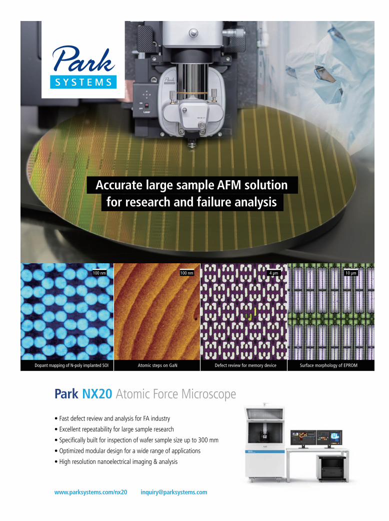
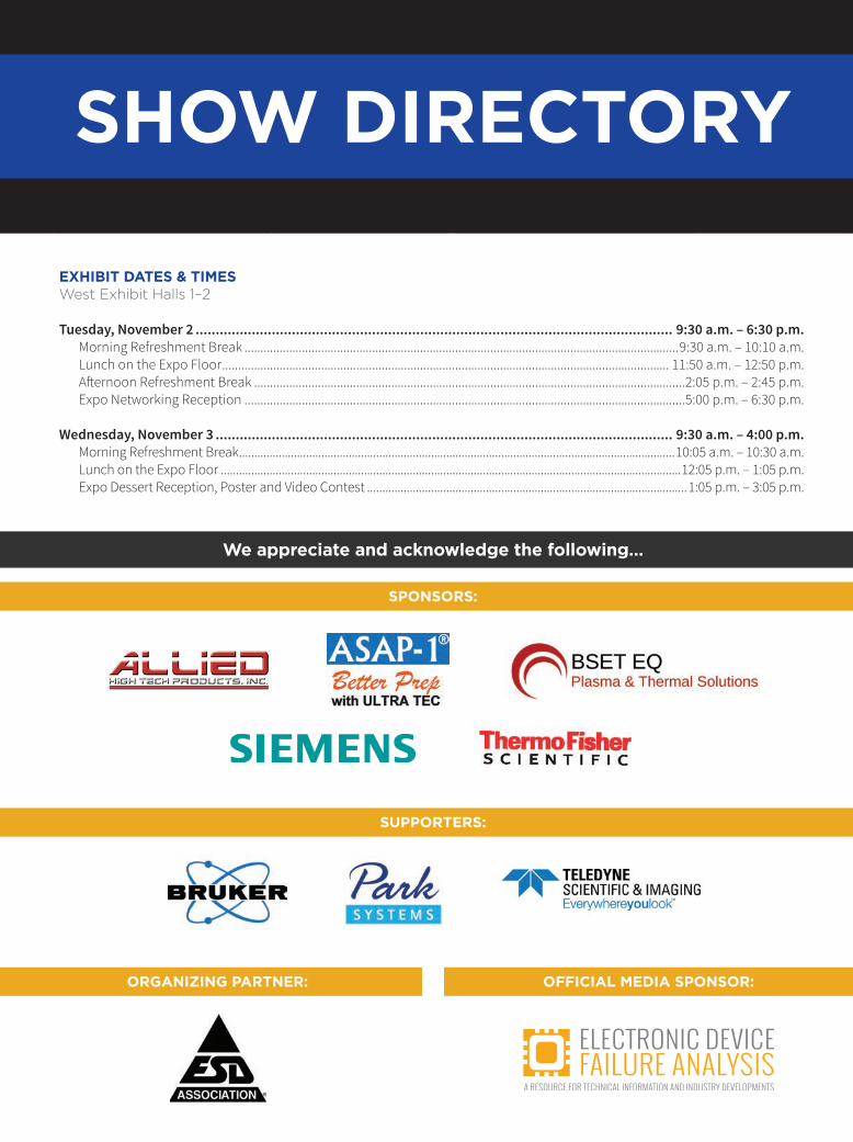
EXHIBIT DATES & TIMESWest Exhibit Halls 1–2
Tuesday, November 2 ....................................................................................................................... 9:30 a.m. – 6:30 p.m.Morning Refreshment Break ........................................................................................................................................9:30 a.m. – 10:10 a.m.Lunch on the Expo Floor ............................................................................................................................................ 11:50 a.m. – 12:50 p.m.Afternoon Refreshment Break .......................................................................................................................................2:05 p.m. – 2:45 p.m.Expo Networking Reception ..........................................................................................................................................5:00 p.m. – 6:30 p.m.
Wednesday, November 3 .................................................................................................................. 9:30 a.m. – 4:00 p.m.
Morning Refreshment Break ...............................................................................................................................................10:05 a.m. – 10:30 a.m.Lunch on the Expo Floor .......................................................................................................................................................12:05 p.m. – 1:05 p.m.Expo Dessert Reception, Poster and Video Contest .........................................................................................................1:05 p.m. – 3:05 p.m.
SHOW DIRECTORY
We appreciate and acknowledge the following…
SPONSORS:
SUPPORTERS:
ORGANIZING PARTNER: OFFICIAL MEDIA SPONSOR:
26IS
TFA
20
21
FIN
AL
PR
OG
RA
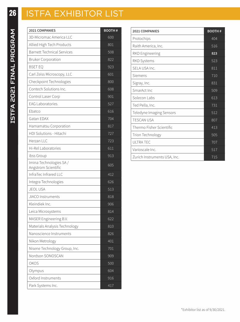
MISTFA EXHIBITOR LIST
2021 COMPANIES BOOTH #
3D-Micromac America LLC 600
Allied High Tech Products 801
Barnett Technical Services 508
Bruker Corporation 822
BSET EQ 923
Carl Zeiss Microscopy, LLC 601
Checkpoint Technologies 800
Contech Solutions Inc. 608
Control Laser Corp 901
EAG Laboratories 527
Ebatco 616
Gatan EDAX 704
Hamamatsu Corporation 817
HDI Solutions - Hitachi 727
Herzan LLC 723
Hi-Rel Laboratories 611
ibss Group 913
Imina Technologies SA / Angstrom Scientific 605
InfraTec Infrared LLC 412
Integra Technologies 626
JEOL USA 513
JIACO Instruments 818
Kleindiek Inc. 906
Leica Microsystems 814
MASER Engineering B.V. 622
Materials Analysis Technology 810
Nanoscience Instruments 826
Nikon Metrology 401
Nisene Technology Group, Inc. 701
Nordson SONOSCAN 909
OKOS 500
Olympus 604
Oxford Instruments 916
Park Systems Inc. 417
2021 COMPANIES BOOTH #
Protochips 404
Raith America, Inc. 516
RKD Engineering 823
RKD Systems 523
SELA USA Inc. 811
Siemens 710
Sigray, Inc. 831
SmarAct Inc 509
Solecon Labs 613
Ted Pella, Inc. 731
Teledyne Imaging Sensors 512
TESCAN USA 807
Thermo Fisher Scientific 413
Trion Technology 505
ULTRA TEC 707
Varioscale Inc. 517
Zurich Instruments USA, Inc. 715
*Exhibitor list as of 9/30/2021.
27IS
TFA
20
21 F
INA
L P
RO
GR
AM
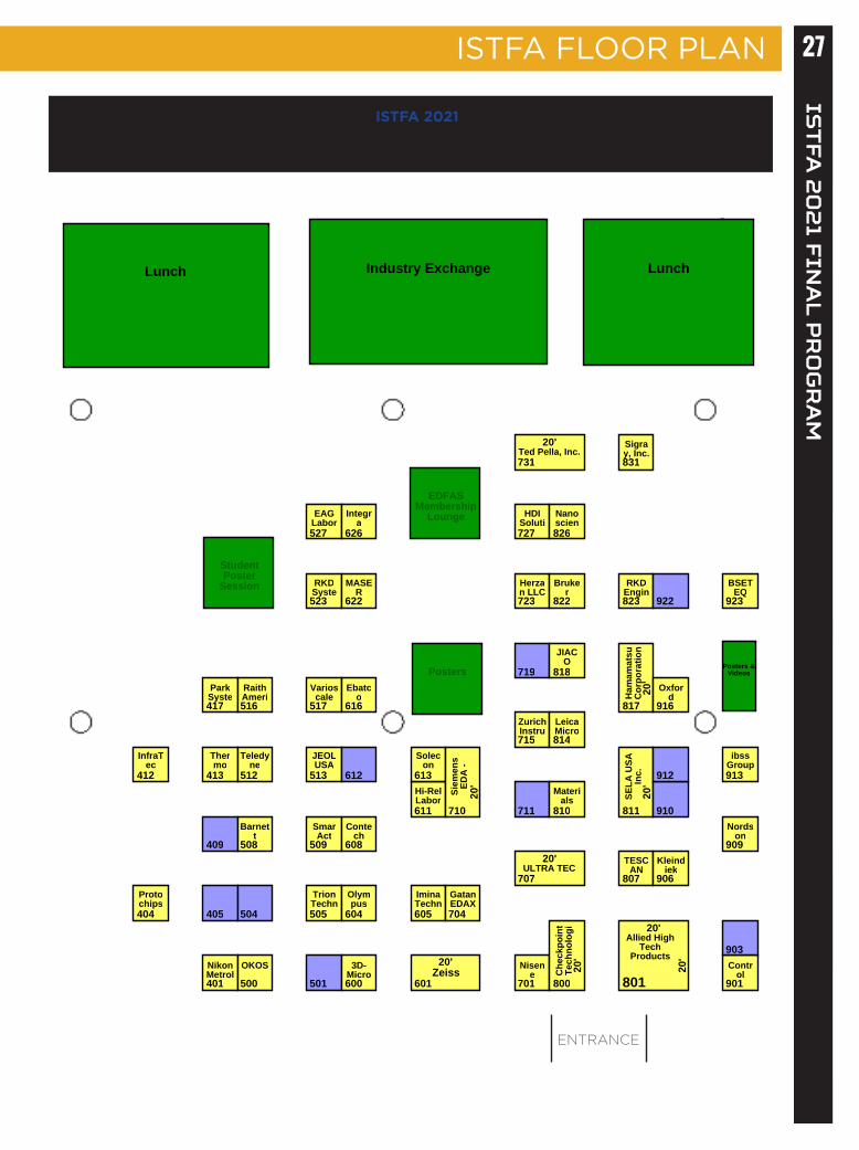
ENTRANCE
StudentPoster
Session
Posters Posters &Videos
EDFASMembership
Lounge
Industry Exchange LunchLunch
401NikonMetrol
404
Protochips
405
409
412
InfraTec
413
Thermo
417ParkSyste
500OKOS
501
504 505
TrionTechn
508Barnet
t509SmarAct
512
Teledyne
513
JEOLUSA
516RaithAmeri
517Varioscale
523RKDSyste
527
EAGLabor
6003D-
Micro601
20'Zeiss
604
Olympus
605
IminaTechn
608Conte
ch
611
Hi-RelLabor
612 613
Solecon
616Ebatc
o
622MASE
R
626
Integra
701Nisen
e
704
GatanEDAX
707
20'ULTRA TEC
710
20'
Siem
ens
EDA
-
711
715ZurichInstru
719
723Herzan LLC
727
HDISoluti
731
20'Ted Pella, Inc.
800
20'
Che
ckpo
int
Tech
nolo
gi
801
20'
20'
Allied HighTech
Products
807TESC
AN
810
Materials
811
20'
SELA
USA
Inc.
814LeicaMicro
817
20'
Ham
amat
suC
orpo
ratio
n
818
JIACO
822Bruke
r823RKD
Engin
826
Nanoscien
831Sigray, Inc.
901Contr
ol
903
906Kleind
iek
909Nords
on
910
912 913
ibssGroup
916Oxfor
d
922 923BSET
EQ
WOMEN MEN
WOMEN
MEN
MEN
WOMEN
STAIRS
STAIRS
ROLL-UP DOOR 2
RO
LL-UP D
OO
R 1B
RO
LL-UP D
OO
R 1A
PAR
TITION
STOR
AG
E
STAIRS
CONCESSION
10 x 30
DOCKOFFICE
ELEVATORLOBBY
ELEVATOR
LOBBY
FIRST AID
SECUREDREG
STORAGE
SERVICEELEVATOR #4
6,000 LBSLIMIT
SERVICEELEVATOR #3
6,000 LBSLIMIT
PASSENGER
ELEVATOR #5
3,000 LBS
LIMIT
PASSENGER
ELEVATOR #6
3,000 LBS
LIMIT
4
5
3
6
51C
1A 1B
2N
1D
ENTRANCE
ISTFA FLOOR PLAN
ISTFA 2021November 2-3, 2021 | Phoenix Convention Center
West Exhibit Halls 1-2
edfas.org
4 3ELECTRONIC DEVICE FAILURE ANALYSIS | VOLUM
E 23 NO. 4
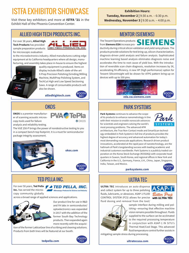
ALLIED HIGH TECH PRODUCTS INC.
BOOTH801
For over 38 years, Allied High Tech Products has provided sample preparation products for microscopic evaluation to the microelectronics industry. Allied manufactures cutting-edge equipment at its California headquarters where all design, manu-facturing, and assembly takes place in-house to ensure the highest
quality equipment is produced. Items on display include Allied’s state-of-the-art X-Prep Precision Polishing/Grinding/Milling Machine, MultiPrep Polishing System, and TechCut High and Low Speed Sectioning Saws. A range of consumable products will also be shown.
alliedhightech.com
Visit these key exhibitors and more at ISTFA '21 in the Exhibit Hall of the Phoenix Convention Center.
Exhibition Hours:Tuesday, November 2 | 9:30 a.m. – 6:30 p.m.
Wednesday, November 3 | 9:30 a.m. – 4:00 p.m.
MENTOR (SIEMENS)
BOOTH710
The Tessent Operations products from Siemens EDA increase pro-ductivity during critical silicon validation and yield ramp phases. The products provide solutions for test bring-up, silicon characterization, diagnosis-driven yield analysis and failure analysis. Sophisticated machine learning based analysis eliminates diagnosis noise and accelerates the time to root cause of yield loss. With the introduc-tion of reversible scan chain diagnosis, resolution increases by 3X, accelerating FA efficiency. A new HP (high performance) option for Tessent SiliconInsight will be shown for ATPG pattern bring-up on devices with up to 330 pins.
eda.sw.siemens.com
ISTFA EXHIBITOR SHOWCASE
OKOSOKOS is a premier manufactur-er of scanning acoustic micros-copy tools used for failure analysis and reliability testing. The VUE 250-P brings the power of nondestructive testing to you in a compact bench-top footprint. It is a must for semiconductor package integrity assessment.
okos.com
BOOTH500
PARK SYSTEMSPark Systems continues to advance the scope of its products to enhance nanometrology in line with their mission to enable nanoscale advances for scientists and engineers solving the world’s most pressing problems. The advanced AFM architecture, the True Non-Contact mode and SmartScan technol-ogy embedded in Park Systems’s full line of products provides the highest degree of accuracy and advanced automation for today’s most demanding nanoscale applications. Research driven product innovations, accelerated at the rapid pace of nanotechnology, are the hallmark of Park’s longstanding success with leading academic and industrial customers worldwide. Park Systems is a publicly traded cor-poration on the Korea Stock Exchange (KOSDAQ) with corporate head-quarters in Suwon, South Korea, and regional offices in New York and California in the U.S., Germany, France, U.K., China, Japan, Singapore, India, Taiwan, and Mexico.
parksystems.comBOOTH
417
TED PELLA INC.For over 50 years, Ted Pella Inc. has served the micros-copy community globally across a broad range of applied sciences and applications.
Our product line for use in R&D and FA labs in semiconductor/ optoelectronics was expanded in 2017 with the addition of the former South Bay Technology products. Then expanded again more recently with the acquisi-
tion of the former LatticeGear line of scribing and cleaving solutions. Products from both lines will be featured at our booth.
tedpella.comBOOTH
731
ULTRA TECULTRA TEC introduces an auto-dispense and collect system for up to three polishing fluids, lubricants, or abrasives. ASAP-1 FLUID CONTROL SYSTEM (FCS) allows for precise fluid dosing and removal from the tool/
sample interface during milling and pol-ishing—ensuring that effective machine vision remains possible throughout. Fluids supplied to the surface can be acclimated to the required processing temperature in conjunction with ASAP-1 IN SITU’s Thermal Heat/Cool Stage. This advanced fluid temperature control further assists in
mitigating sample stress during processing.
ultratecusa.comBOOTH
417
29IS
TFA
20
21 F
INA
L P
RO
GR
AM
NOTES
30IS
TFA
20
21
FIN
AL
PR
OG
RA
MTOOLS OF THE TRADE TOUR
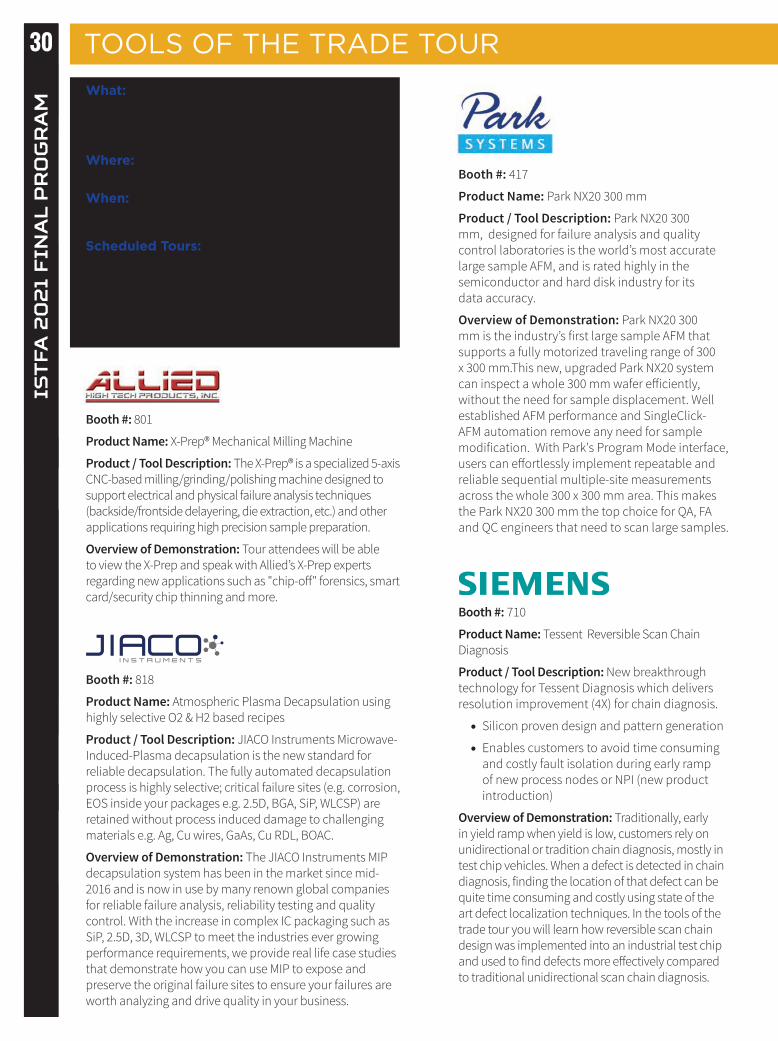
Booth #: 801
Product Name: X-Prep® Mechanical Milling Machine
Product / Tool Description: The X-Prep® is a specialized 5-axis CNC-based milling/grinding/polishing machine designed to support electrical and physical failure analysis techniques (backside/frontside delayering, die extraction, etc.) and other applications requiring high precision sample preparation.
Overview of Demonstration: Tour attendees will be able to view the X-Prep and speak with Allied’s X-Prep experts regarding new applications such as "chip-off" forensics, smart card/security chip thinning and more.
Booth #: 818
Product Name: Atmospheric Plasma Decapsulation using highly selective O2 & H2 based recipes
Product / Tool Description: JIACO Instruments Microwave-Induced-Plasma decapsulation is the new standard for reliable decapsulation. The fully automated decapsulation process is highly selective; critical failure sites (e.g. corrosion, EOS inside your packages e.g. 2.5D, BGA, SiP, WLCSP) are retained without process induced damage to challenging materials e.g. Ag, Cu wires, GaAs, Cu RDL, BOAC.
Overview of Demonstration: The JIACO Instruments MIP decapsulation system has been in the market since mid-2016 and is now in use by many renown global companies for reliable failure analysis, reliability testing and quality control. With the increase in complex IC packaging such as SiP, 2.5D, 3D, WLCSP to meet the industries ever growing performance requirements, we provide real life case studies that demonstrate how you can use MIP to expose and preserve the original failure sites to ensure your failures are worth analyzing and drive quality in your business.
Booth #: 417
Product Name: Park NX20 300 mm
Product / Tool Description: Park NX20 300 mm, designed for failure analysis and quality control laboratories is the world’s most accurate large sample AFM, and is rated highly in the semiconductor and hard disk industry for its data accuracy.
Overview of Demonstration: Park NX20 300 mm is the industry’s first large sample AFM that supports a fully motorized traveling range of 300 x 300 mm.This new, upgraded Park NX20 system can inspect a whole 300 mm wafer efficiently, without the need for sample displacement. Well established AFM performance and SingleClick-AFM automation remove any need for sample modification. With Park's Program Mode interface, users can effortlessly implement repeatable and reliable sequential multiple-site measurements across the whole 300 x 300 mm area. This makes the Park NX20 300 mm the top choice for QA, FA and QC engineers that need to scan large samples.
Booth #: 710
Product Name: Tessent Reversible Scan Chain Diagnosis
Product / Tool Description: New breakthrough technology for Tessent Diagnosis which delivers resolution improvement (4X) for chain diagnosis.
• Silicon proven design and pattern generation
• Enables customers to avoid time consuming and costly fault isolation during early ramp of new process nodes or NPI (new product introduction)
Overview of Demonstration: Traditionally, early in yield ramp when yield is low, customers rely on unidirectional or tradition chain diagnosis, mostly in test chip vehicles. When a defect is detected in chain diagnosis, finding the location of that defect can be quite time consuming and costly using state of the art defect localization techniques. In the tools of the trade tour you will learn how reversible scan chain design was implemented into an industrial test chip and used to find defects more effectively compared to traditional unidirectional scan chain diagnosis.
What:Demonstrations of the latest products and services. Learn useful information and see firsthand the latest tools in the industry. See equipment in action right on the show floor.
Where:Expo Show Floor – West Halls 1-2
When:Monday, November 1, 2021 | 5:00 p.m. – 6:45 p.m.
Scheduled Tours:Allied High TechJIACOPark SystemsRKD Systems
Must Register in Advance to Attend
SELASiemens ULTRA TEC
31IS
TFA
20
21 F
INA
L P
RO
GR
AM
TOOLS OF THE TRADE TOUR
Booth #: 707
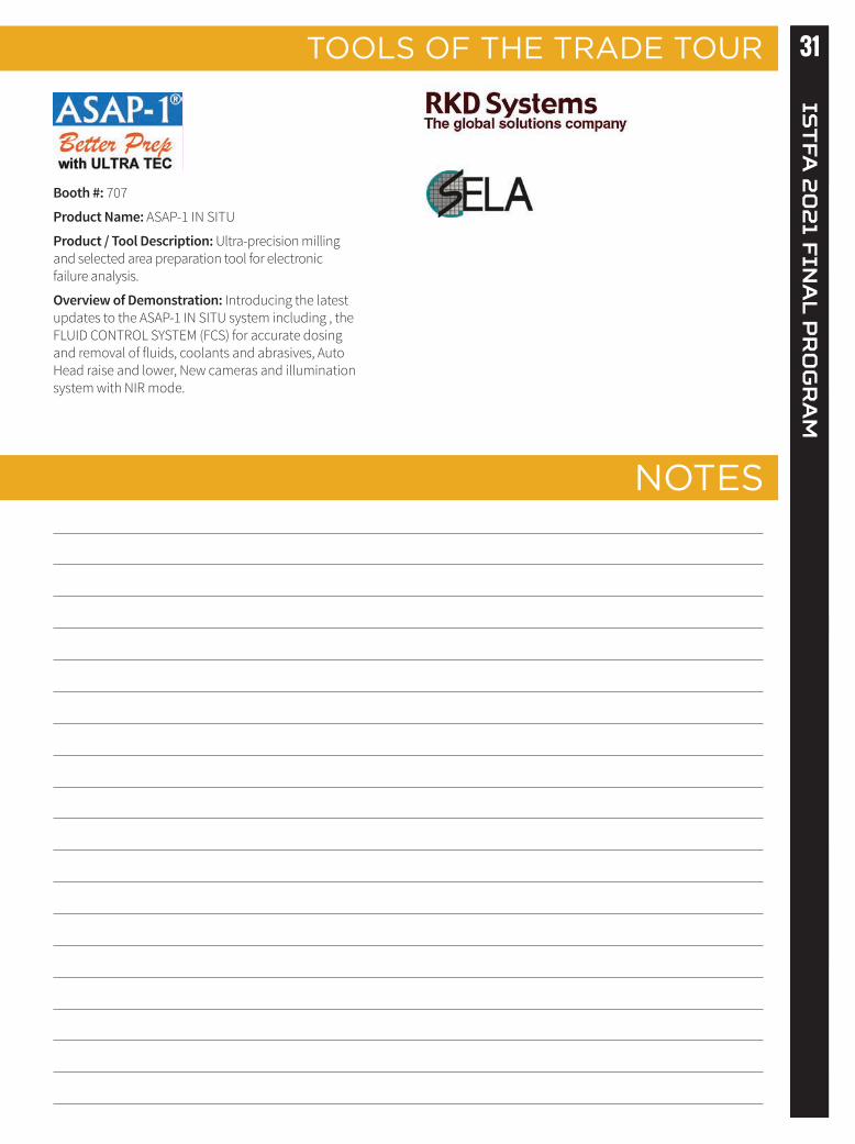
Product Name: ASAP-1 IN SITU
Product / Tool Description: Ultra-precision milling and selected area preparation tool for electronic failure analysis.
Overview of Demonstration: Introducing the latest updates to the ASAP-1 IN SITU system including , the FLUID CONTROL SYSTEM (FCS) for accurate dosing and removal of fluids, coolants and abrasives, Auto Head raise and lower, New cameras and illumination system with NIR mode.
NOTES

Toll Free (US) 1-877-542-0609Tel: 1-714-542-0608 Fax: 1-714-542-0627
e-mail: [email protected]
EXPANDING THE SAMPLE PREP TOOLKIT
‘In Situ’ RST Measurement- Single footprint system solution- Eliminates tilt/curve translation errors
Two RST Versions available- STANDARD NIR- ULTRATHIN
Ultra-High Res CamerasTarget,
45° Side 45° Front- NEW
Work with Overlays
Rotate, Stretch, Resize Layer-Locking
Unique Legacy Modules
5-AXIS DIGITAL MILL & POLISHER
MEET 3D & CURVED/WARPEDSURFACE CHALLENGES WITH
ADAPTIVE MODULES
Combined Mapping & Polishing Control
NEW Fluid Control System
Interactive Overlay Controls
ASAP-1-InSitu.indd 1 06/21/21 7:00 PM
33IS
TFA
20
21 F
INA
L P
RO
GR
AM
Toll Free (US) 1-877-542-0609Tel: 1-714-542-0608 Fax: 1-714-542-0627
e-mail: [email protected]
EXPANDING THE SAMPLE PREP TOOLKIT
‘In Situ’ RST Measurement- Single footprint system solution- Eliminates tilt/curve translation errors
Two RST Versions available- STANDARD NIR- ULTRATHIN
Ultra-High Res CamerasTarget,
45° Side 45° Front- NEW
Work with Overlays
Rotate, Stretch, Resize Layer-Locking
Unique Legacy Modules
5-AXIS DIGITAL MILL & POLISHER
MEET 3D & CURVED/WARPEDSURFACE CHALLENGES WITH
ADAPTIVE MODULES
Combined Mapping & Polishing Control
NEW Fluid Control System
Interactive Overlay Controls
ASAP-1-InSitu.indd 1 06/21/21 7:00 PM
3D-Micromac America LLC ................................................................................................................................. 6003D-Micromac AG is the industry leader in laser micromachining. We develop processes and laser systems with superior production efficiency. 3D-Micromac systems have been successfully implemented in various high-tech industries worldwide including semiconductor industry and microdiagnostics. In the area of sample preparation, 3D-Micromac has developed the microPREP PRO system that provides efficient laser-based preparation to a broad range of microstructure diagnostics techniques.www.3d-micromac.com
Allied High Tech Products .................................................................................................................................. 801For over 38 years, Allied High Tech Products has provided sample preparation products for microscopic evaluation. Items on display include Allied's state-of-the-art X-Prep® Precision Polishing/Grinding/Milling Machine, MultiPrep™ Polishing System, sectioning saws and a range of consumable products. Visit Booth #801 in the exhibit hall.www.alliedhightech.com
Barnett Technical Services ................................................................................................................................ 508Barnett Technical Services is the North American Distributor for Micro Support micromanipulators. Our systems facilitate micro-sample handling. Specifically for ISTFA-related applications, our systems can perform electrical measurements on pads as small as one micron.www.barnett-technical.com
Bruker Corporation ........................................................................................................................................... 822www.bruker.com/nano
BSET EQ ............................................................................................................................................................ 923BSET EQ provides solutions for your FA needs through GAS PLASMA and LASER technologies. On display is our PLASER™ plasma DECAP system and our LASER DECAP tools. BSET EQ is the leader of this DECAP technology with continued development and prior art since 1999. Recently we have proven to be by far the best with exposure of SILVER architectures. Also highlighted is our popular FA2000 tabletop / FA3000 RIE/ICP etchers. These systems provide functional delayering for your packaged devices or wafers.www.bsetplasmas.com
Carl Zeiss Microscopy, LLC ................................................................................................................................. 601ZEISS is a leading supplier for the global semiconductor industry, providing advanced 3D imaging solutions for failure analysis and process development. Our broad product portfolio includes X-ray, electron, ion and light microscopy solutions for semiconductor and electronic applications.www.zeiss.com/pcs
Checkpoint Technologies .................................................................................................................................. 800Checkpoint Technologies develops and manufactures innovative optical failure analysis tools used by semiconductor manufacturers to improve the speed and reliability of integrated circuits. Our products, which range from OEM components to fully-integrated, end-user solutions, reflect our fundamental commitment to maximizing value by adapting technology to meet specific market needs.www.checkpointtechnologies.com
Contech Solutions Inc. ...................................................................................................................................... 608Contech Solutions Inc is a leader in design and manufacturing of Semi-conductor test interface products. At Contech Solutions we are committed to quality, customer satisfaction and delivery of superior products.www.contechsolutions.com
Control Laser Corp ............................................................................................................................................ 901Our FALIT® (FA-Light) Failure Analysis Laser Inspection Tools are specifically designed with the semiconductor failure analysis and forensics labs in mind. Our laser tools are used for IC decapsulation, gel removal, cross-sectioning, and delidding components. By using our patented process, you can reduce your acid usage by more than 90%!www.controllaser.com
COMPANY DESCRIPTIONS
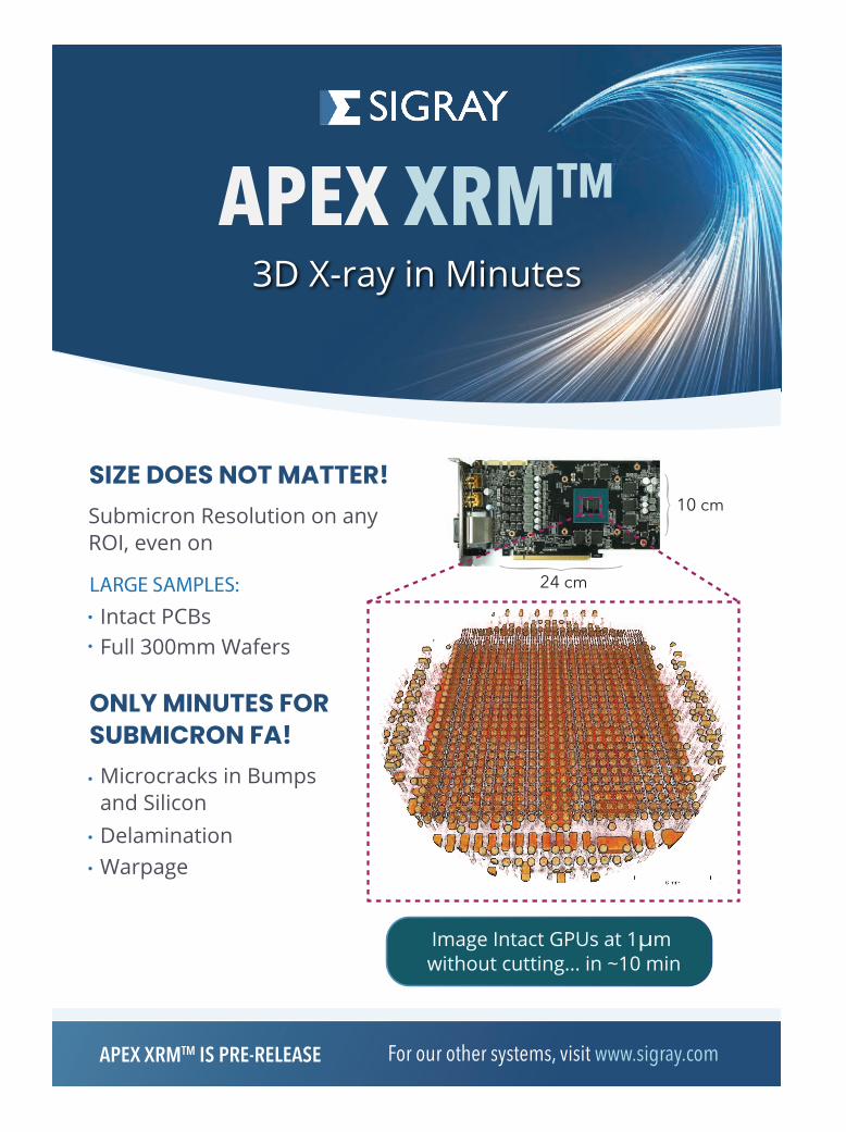
3D X-ray in Minutes
Submicron Resolution on any ROI, even on
Intact PCBsFull 300mm Wafers
LARGE SAMPLES:
APEX XRMTM IS PRE-RELEASE
Microcracks in Bumps and SiliconDelaminationWarpage
Image Intact GPUs at 1μm without cutting... in ~10 min
For our other systems, visit www.sigray.com
APEX XRMTM
10 cm
24 cm
}}
35IS
TFA
20
21 F
INA
L P
RO
GR
AM
EAG Laboratories ............................................................................................................................................... 527EAG Laboratories, the leader for Electrical Test, Failure Analysis, Reliability and Materials Analysis. EAG reduces cycle time, cost of new product introduction, and supports your test and analysis needs throughout the life cycle of your products. All backed by EAG’s extensive capital equipment, infrastructure, and engineering expertise.www.eag.com
Ebatco ............................................................................................................................................................... 616Ebatco is a leading service lab that provides failure analysis for electronics, IC, and semiconductor industrial customers. Ebatco is recognized for working with surfaces, interfaces, ultra-thin films, small volumes and miniaturized devices. Contact us for nanoscale analyses, material characterization, surface contamination issues, failure mode and root cause determination. Ebatco promises prompt solutions through great lab services, expert-level consultation, and advanced instruments.www.ebatco.com
Gatan EDAX ....................................................................................................................................................... 704Gatan and EDAX are the world's leading manufacturers of instrumentation and software for electron microscopes. Gatan and EDAX products are used in a broad range of failure analysis applications, including those for semiconductors (micro- and nano-electronics), nano-materials, and optoelectronic devices. Gatan and EDAX are members of AMETEK’s Electronic Instruments Group (EIG) - a leader in advanced analytical, monitoring, testing, calibrating and display instrumentation.www.gatan.com
Hamamatsu Corporation ................................................................................................................................... 817Hamamatsu Corporation is the North American subsidiary of Hamamatsu Photonics K.K. (Japan), a leading manufacturer of devices for the generation and measurement of infrared, visible, UV light, and x-rays. We offer specialized systems for semiconductor failure analysis and other applications. We also offer photomultiplier tubes, photodiodes, image sensors, cameras, and light sources.www.hamamatsu.com
HDI Solutions - Hitachi ...................................................................................................................................... 727www.hdi-solutions.com
Herzan LLC ........................................................................................................................................................ 723Our mission is to help researchers achieve more from their instrumentation by removing disruptive environmental noise from their measurements. We specialize in delivering high-performance solutions that significantly reduce acoustics, vibrations, and AC/DC Fields, including: active vibration isolation platforms, acoustic enclosures, and magnetic field cancellation systems. These solutions have been chosen by thousands of users worldwide to protect their research in the noisiest environments.
Hi-Rel Laboratories ........................................................................................................................................... 611Located in Spokane, Washington, Hi-Rel Laboratories is an independently owned and operated corporation, whose main concentration of activity is in the materials evaluation of the micro-electronic oriented phases of commercial, aerospace and defense industries.www.hrlabs.com
ibss Group ......................................................................................................................................................... 913The GV10x Downstream Asher and Mobile Cubic Asher reduce carbon & hydrocarbon contamination 10 to 20 times more effectively than traditional methods at vacuum pressures. Artifacts in SEM images are gone; the microscope maintains high resolution and beam stability. Black scan squares are eliminated in SEM images. Carbon contamination in FIB and TEM systems can be controlled as well.www.ibssgroup.com
Imina Technologies SA / Angstrom Scientific ..................................................................................................... 605Angstrom Scientific Inc. provides materials characterization solutions including: Imina Nano-manipulators and probe stations, Point Electronic EBIC/EBAC, Hitachi Tabletop-SEM/EDX & FlexSEM, Deben Tensile Stages & SEM Accessories, Leica EM Sample Prep Equipment, KA Imaging Micro CT, STOE X-Ray systems, EMSIS TEM cameras, QD In-Situ AFM, Amsterdam Scientific Imaging Detection. Visit Booth 605 and/or www.angstrom.us.www.angstrom.us
COMPANY DESCRIPTIONS
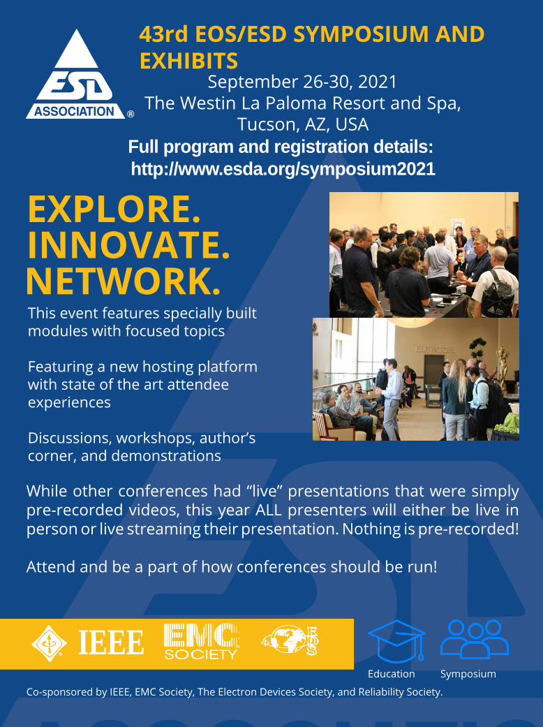
EXPLORE.
While other conferences had “live” presentations that were simply pre-recorded videos, this year ALL presenters will either be live in person or live streaming their presentation. Nothing is pre-recorded! Attend and be a part of how conferences should be run!
INNOVATE.This event features specially built modules with focused topics Featuring a new hosting platform with state of the art attendee experiences Discussions, workshops, author’s corner, and demonstrations
NETWORK.
Co-sponsored by IEEE, EMC Society, The Electron Devices Society, and Reliability Society.
IEEE
43rd EOS/ESD SYMPOSIUM AND EXHIBITS
The Westin La Paloma Resort and Spa, Tucson, AZ, USA
September 26-30, 2021
Education Symposium
Full program and registration details: http://www.esda.org/symposium2021
37IS
TFA
20
21 F
INA
L P
RO
GR
AM
InfraTec Infrared LLC ......................................................................................................................................... 412
Integra Technologies ......................................................................................................................................... 626Integra Technologies is a US based full turn-key provider of die preparation, packaging, electrical testing and characterization of components and related value-added services, for the Commercial, Medical, Automotive, Industrial, Semiconductor and Aerospace industries. Integra offers die prep, advanced packaging, screening, qualification, DPA and failure analysis services. For more about Integra’s services, please visit www.integra-tech.com.www.integra-tech.com
JEOL USA .......................................................................................................................................................... 513JEOL is the global leader in ultra-high resolution electron microscopes and tools for failure analysis, quality control, product inspection and semiconductor/nanotech R&D. SEMs and TEMs providing high throughput analysis, nanoscale/atomic imaging, and high-speed mapping are available. Learn about our new solutions including correlative microscopy, surface analyzers, specimen prep and analytical equipment to support your requirements.www.jeolusa.com
JIACO Instruments ............................................................................................................................................ 818JIACO Instruments Microwave-Induced-Plasma decapsulation is the new standard for reliable Failure Analysis and Quality Control. The fully automated process is highly selective; critical failure sites in advanced packages (e.g. SiP, WLCSP, 2.5D, 3D) are retained without process induced damage to challenging materials e.g. Ag, Cu bond wire, GaAs, Cu RDL, BOAC.www.jiaco-instruments.com
Kleindiek Inc. .................................................................................................................................................... 906www.kleindiek.us
Leica Microsystems ........................................................................................................................................... 814Leica Microsystems develops and manufactures microscopes and scientific instruments for the analysis of microstructures and nanostructures. The company is one of the market leaders in compound and stereo microscopy, digital microscopy, confocal laser scanning microscopy, electron microscopy sample preparation, optical coherence tomography, and surgical microscopes.leica-microsystems.com
MASER Engineering B.V. ..................................................................................................................................... 622MASER Engineering is an independent engineering service provider for reliability test and failure analysis of micro-electronic components and systems. We offer advanced facilities for Integrated Device Manufacturers, Fabless and Labless IC manufacturers as well as the Original Equipment Manufacturing companies in our main lab in Enschede, The Netherlands.www.maser.nl
Materials Analysis Technology ........................................................................................................................... 810Founded in 2002, Materials Analysis Technology Inc. (MA-tek) is a world-class laboratory providing services in materials analysis. In line with the exponential rate of the business’s development, MA-tek has successfully expanded to be equipped with additional Failure Analysis and Reliability Testing services. These integrations allow for MA-tek to provide superior service for its customers in various industries.www.ma-tek.com
Nanoscience Instruments .................................................................................................................................. 826For over 15 years, Nanoscience Instruments has become a trusted supplier of the most innovative and highest quality analytical solutions to academia and industry. We specialize in surface science and instrumentation for nanoscale applications. We also offer contract analytical services. Visit booth #809 to learn about our ion mills, desktop scanning electron microscopes, correlative microscopes, nanoindenters, optical profilometers, QCM, tensiometers, AFMs, and electrospinning equipment.www.nanoscience.com
Nikon Metrology ................................................................................................................................................ 401Nikon Metrology offers the most complete and innovative metrology product portfolio, including state-of-the-art vision measuring instruments complemented with optical inspection and mechanical 3D metrology solutions. These reliable and innovative products respond to the advanced inspection requirements of manufacturers active in consumer, automotive, aerospace, electronics, medical and other industries.www.nikonmetrology.com
COMPANY DESCRIPTIONS
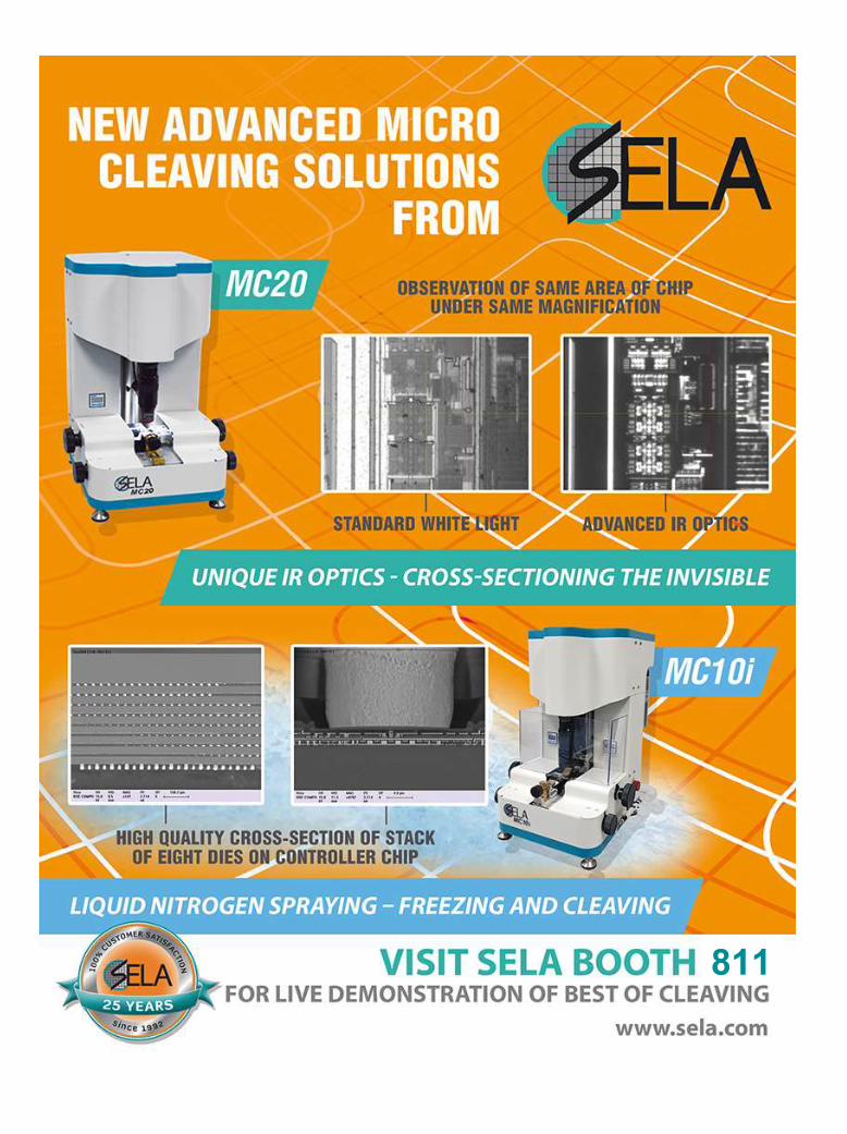
39IS
TFA
20
21 F
INA
L P
RO
GR
AM
Nisene Technology Group, Inc. .......................................................................................................................... 701Nisene Technology Group is the world leader in automated integrated circuit decapsulation. In the 30-plus years in the industry — now spanning five decades — Nisene has developed and advanced their patented technology from its humble beginning with the original Jet Etch, through the 350 series, and now with our latest product line: the JetEtch Pro family of decappers.www.nisene.com
Nordson SONOSCAN .......................................................................................................................................... 909Nordson DAGE and SONOSCAN, units of the Nordson Corporation (NASDAQ: NDSN) manufacture and support an award-winning portfolio of X-ray Inspection, Bond Test and Acoustic Micro Imaging systems. Nordson’s family of Test and Inspection products which also include AOI and Wafer X-ray Metrology bring powerful and cost-effective solutions to the Printed Circuit Board Assembly (PCBA) and Semiconductor industries.www.nordsondage.com
OKOS ................................................................................................................................................................. 500 www.okos.com
Olympus ............................................................................................................................................................ 604Come and experience a hands-on demonstration of Olympus’ newest advanced optical imaging system, the OLS5100. Built for failure analysis and material engineering research, the OLS5100 laser microscope combines exceptional measurement accuracy and optical performance with smart tools that make the microscope easy to use. Precisely measure shape and surface roughness at the submicron level quickly and efficiently to simplify your workflow with data you can trust.www.olympus-ims.com
Oxford Instruments ........................................................................................................................................... 916Oxford Instruments NanoAnalysis provides leading-edge tools that enable materials characterization and sample manipulation at the nanometer scale. Used on electron microscopes (SEM and TEM) and ion-beam systems (FIB), our tools are used for R&D across a wide range of academic and industrial applications including semiconductors, renewable energy, mining, metallurgy, and forensics.www.oxford-instruments.com
Park Systems Inc. .............................................................................................................................................. 417Park Systems is a world-leading manufacturer of atomic force microscopy (AFM) systems with a complete range of products for researchers and industry engineers in the biology, materials research, semiconductor and data storage industries. Park’s AFM provides the highest data accuracy at nanoscale resolution, superior productivity, and the lowest operating cost, thanks to its unique technology and innovative engineering. Please visit parksystems.com for more information.www.parksystems.com
Protochips......................................................................................................................................................... 404www.protochips.com
Raith America, Inc. ............................................................................................................................................ 516Raith is a leading precision technology manufacturer for large area SEM image acquisition, electron beam lithography, focused ion beam nanofabrication and nanoengineering. Reverse engineering of semiconductor devices strongly benefits from the large area imaging performance that the automation and stability of a professional lithography system architecture, the capability of precise image calibrations and the accuracy of the employed Laser Interferometer controlled Stage (LIS) are enabling.
RKD Engineering ............................................................................................................................................... 823RKD Engineering Corp, Inc. offers the full range of mixed acid and solutions decapsulators for gold, copper, aluminum and silver wire bonded packages.www.rkdengineering.com
RKD Systems ..................................................................................................................................................... 523High Precision, high speed milling systems to remove IC packages from either a PC board or a chip onFlex while keeping the ball bonds intact. High precision die thinning and polishing down to less than a micron. The ability to measure remaining silicon thickness to 0.5 microns
COMPANY DESCRIPTIONS
40IS
TFA
20
21
FIN
AL
PR
OG
RA
M
SELA USA Inc. .................................................................................................................................................... 811Full range of cleaving solutions. For over 25 years SELA develops and delivers advanced cleaving solutions for failure analysis and yield management in the semiconductor industry and analytical purposes in research laboratories and universities around the world. SELA’s patented Nano Cleaving, Micro Cleaving and Perfect Cleaving technologies address emerging and challenging requirements of the cross-section for a wide variety of structures, materials and substrates.www.sela.com
Siemens ............................................................................................................................................................ 710Tessent® silicon learning software provides a unique advantage to accelerate defect identification in digital semiconductor devices. The Tessent Diagnosis and YieldInsight capabilities deliver unprecedented results to accelerate yield learning for the most challenging advanced process nodes.https://eda.sw.siemens.com/en-US/ic/tessent/
Sigray, Inc. ........................................................................................................................................................ 831www.sigray.com
SmarAct Inc ....................................................................................................................................................... 509SmarAct develops and produces piezo-based, high-accuracy positioning and measuring systems for industrial and research applications in the micro- and nanometer scale. Comprehensive positioner systems with numerous degrees of freedom and parallel kinematics, microscopy stages and laser interferometers can be assembled to custom-built, complete robotic systems, and work under extreme conditions, e.g., ultrahigh vacuum, cryogenic temperatures, and non-magnetic materials. Solecon Labs ..................................................................................................................................................... 613Our expertise is in Spreading Resistance Analysis. We provide front-end process engineers/scientists with timely and cost-effective characterization of resistivity and concentration vs depth profiles, with resolutions down to the nanometer range. SRA is especially useful for is depth accuracy (+/-3%) and sensitivity to ultra-low dopant concentrations. SRA is helpful for checking the results for, epitaxial deposition, ion implant verification, dopant contamination and diffusions in general.www.solecon.com
Ted Pella, Inc. .................................................................................................................................................... 731Ted Pella, Inc is focused on supplying items in support of sample preparation and fixturing for all forms of microscopy. These range from the former Southbay Technology line and our PELCO branded instruments through to TEM grids, specimen handling tools and storage devices, polishing consumables, spatial and elemental calibration standards to name just a few.www.tedpella.com
Teledyne Imaging Sensors ................................................................................................................................. 512www.teledyne-si.com
TESCAN USA ...................................................................................................................................................... 807TESCAN is a global supplier of Scanning Electron Microscopes and associated technologies and the company has a strong reputation and brand name in the field of designing and manufacturing system solutions for many different applications. The company is focused on research, development and manufacture of Scanning Electron Microscopes, Focused ion beam systems, X-Ray CT systems and supplementary accessories for SEMs, image processing, custom systems, and software development.www.tescan-usa.com
Thermo Fisher Scientific .................................................................................................................................... 413Thermo Fisher Scientific provides workflows for semiconductor Failure Analysis and Research Labs to meet the needs of Analog, MEMS, Logic, Memory, Foundry, Packaging and Display markets. Our solutions include automated, high-productivity TEM/TEM sample prep that provide zero-damage, low-z imaging and characterization; innovative Chemical, Electrical and Physical Failure Analysis, and Compliance Testing systems to localize subtle electrical issues that affect yield, performance or reliability.www.thermofisher.com/EM
COMPANY DESCRIPTIONS
41IS
TFA
20
21 F
INA
L P
RO
GR
AM
Trion Technology ............................................................................................................................................... 505Manufacturer of a wide variety of custom Plasma Etch, Strip and Deposition Equipment for the Compound Semiconductor, MEMS, Opto-Electronic and other markets. Our products have the smallest footprint and lowest cost systems with proven production reliability. If you wish anything from full-blown production cluster tools to a simple laboratory system, Trion makes it. www.triontech.com
ULTRA TEC ......................................................................................................................................................... 707ULTRA TEC is a designer, manufacturer and supplier of surface and sample preparation equipment for the world's failure analysis and related high tech fields. Our ASAP-1 product line has become the de-facto standard for selected area preparation, backside thinning and mechanical decap applications. Our ULTRAPOL line of polishers provides key advantages for cross-section, parallel polishing and backside thinning. We provide microscopy tools and a wide range of consumables to support our products.www.ultratecusa.com
Varioscale Inc. ................................................................................................................................................... 517varioscale.com
Zurich Instruments USA, Inc. ............................................................................................................................. 715Zurich Instruments is a test and measurement company based in Zurich, Switzerland, developing and selling measurement instruments and delivering customer support in key markets around the world, either directly or with carefully selected partners. We make cutting-edge instrumentation for scientists and technologists in advanced labs who are passionate about phenomena that are often notoriously difficult to measure.www.zhinst.com
COMPANY DESCRIPTIONS
NOTES
ORGANIZED BY:
Chasing Ever-smaller and More Elusive Defects
2022October 30–November 3 | Pasadena, California
The demand for higher performance and lower power-consumption microelectronic devices has driven semiconductor technology to shrink continuously according to Moore’s Law. Furthermore, with nanotechnologies, a set of disruptive developments in new structures and novel materials was introduced. Thus, the defects that cause semiconductor device failures have become smaller and more elusive. To chase such defects, all failure analysis techniques and methodologies also need to be improved to keep pace with semiconductor technology. Failure characterization, fault isolation, electrical failure analysis, physical analysis, microscope imaging, and materials analysis are examples of the key challenges. A gap analysis has been done by the EDFAS FA Technology Roadmap Committee and is available on ASM Connect.
CALL FOR PAPERS WILL OPEN NOVEMBER 2021. Plan to attend ISTFA 2022 today!
istfaevent.org
43IS
TFA
20
21 F
INA
L P
RO
GR
AM
Analytical Probe Stations (Instruments, Equipment, Accessories)Barnett Technical Services ....................................................508BSET EQ .....................................................................................923Checkpoint Technologies ......................................................800Contech Solutions Inc. ...........................................................608Herzan LLC ................................................................................723Imina Technologies SA / .......................................................605Angstrom ScientificIntegra Technologies ..............................................................626Materials Analysis Technology .............................................810Nanoscience Instruments .....................................................826Olympus .....................................................................................604Park Systems Inc. .....................................................................417SmarAct Inc ...............................................................................509Thermo Fisher Scientific ........................................................413ULTRA TEC .................................................................................707
DUT Boards & FixturesContech Solutions Inc. ...........................................................608
Failure Analysis Laser Cutter: Micro Electronics LaserBSET EQ .....................................................................................923Control Laser Corp ..................................................................901EAG Laboratories .....................................................................527Gatan EDAX ...............................................................................704Integra Technologies ..............................................................626Materials Analysis Technology .............................................810
Failure Analysis Test SocketsBSET EQ .....................................................................................923Contech Solutions Inc. ...........................................................608EAG Laboratories .....................................................................527Integra Technologies ..............................................................626Materials Analysis Technology .............................................810
FTIR EquipmentBarnett Technical Services ....................................................508EAG Laboratories .....................................................................527Hamamatsu Corporation ......................................................817Materials Analysis Technology .............................................810Thermo Fisher Scientific ........................................................413
Image Analysis Systems & SoftwareAllied High Tech Products .....................................................801BSET EQ .....................................................................................923Carl Zeiss Microscopy, LLC.....................................................601Checkpoint Technologies ......................................................800EAG Laboratories .....................................................................527Gatan EDAX ...............................................................................704Integra Technologies ..............................................................626JEOL USA ...................................................................................513Leica Microsystems .................................................................814Nanoscience Instruments .....................................................826Nordson SONOSCAN ..............................................................909Park Systems Inc. .....................................................................417TESCAN USA .............................................................................807Thermo Fisher Scientific ........................................................413ULTRA TEC .................................................................................707
Infrared Thermal Imaging Systems: Thermal Inducing SystemsEAG Laboratories .....................................................................527Materials Analysis Technology .............................................810Thermo Fisher Scientific ........................................................413ULTRA TEC .................................................................................707
Laser Signal Injection MicroscopyBSET EQ .....................................................................................923Checkpoint Technologies ......................................................800EAG Laboratories .....................................................................527Thermo Fisher Scientific ........................................................413
Microanalysis and Digital Imaging Systems for Materials AnalysisAllied High Tech Products .....................................................801Applied Beams .........................................................................711Barnett Technical Services ....................................................508BSET EQ .....................................................................................923Carl Zeiss Microscopy, LLC.....................................................601Control Laser Corp ..................................................................901EAG Laboratories .....................................................................527Ebatco ........................................................................................616Gatan EDAX ...............................................................................704Herzan LLC ................................................................................723Leica Microsystems .................................................................814Materials Analysis Technology .............................................810Olympus .....................................................................................604Oxford Instruments .................................................................916Park Systems Inc. .....................................................................417Thermo Fisher Scientific ........................................................413
Microscopes (Scanning Electron, Acoustic, Confocal, Upright, Inverted & Stereo)Allied High Tech Products .....................................................801Applied Beams .........................................................................711Barnett Technical Services ....................................................508Carl Zeiss Microscopy, LLC.....................................................601Checkpoint Technologies ......................................................800EAG Laboratories .....................................................................527Herzan LLC ................................................................................723ibss Group .................................................................................913Imina Technologies SA / .......................................................605Angstrom ScientificJEOL USA ...................................................................................513Leica Microsystems .................................................................814Materials Analysis Technology .............................................810Nanoscience Instruments .....................................................826Nikon Metrology .......................................................................401Nordson SONOSCAN ..............................................................909Olympus .....................................................................................604Oxford Instruments .................................................................916Raith America, Inc. ...................................................................516SmarAct Inc ...............................................................................509Ted Pella, Inc. ............................................................................731TESCAN USA .............................................................................807Thermo Fisher Scientific ........................................................413ULTRA TEC .................................................................................707
PRODUCTS & SERVICES INDEX
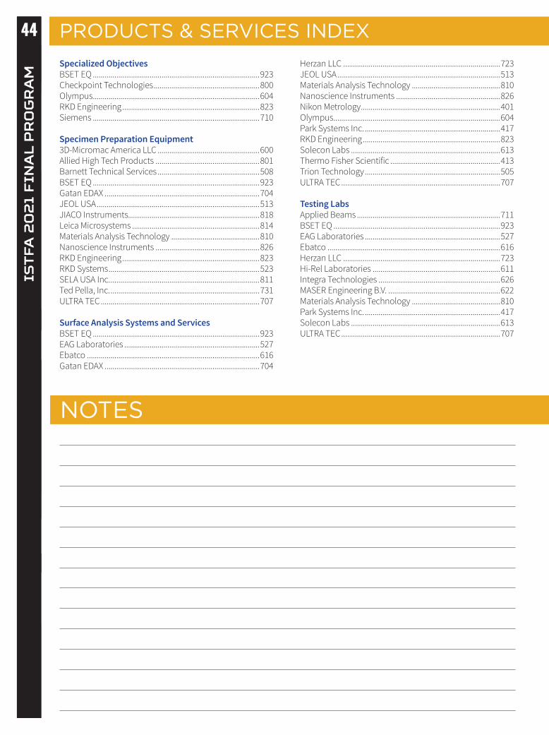
44IS
TFA
20
21
FIN
AL
PR
OG
RA
MPRODUCTS & SERVICES INDEXSpecialized ObjectivesBSET EQ .....................................................................................923Checkpoint Technologies ......................................................800Olympus .....................................................................................604RKD Engineering ......................................................................823Siemens .....................................................................................710
Specimen Preparation Equipment3D-Micromac America LLC ....................................................600Allied High Tech Products .....................................................801Barnett Technical Services ....................................................508BSET EQ .....................................................................................923Gatan EDAX ...............................................................................704JEOL USA ...................................................................................513JIACO Instruments...................................................................818Leica Microsystems .................................................................814Materials Analysis Technology .............................................810Nanoscience Instruments .....................................................826RKD Engineering ......................................................................823RKD Systems .............................................................................523SELA USA Inc. ............................................................................811Ted Pella, Inc. ............................................................................731ULTRA TEC .................................................................................707
Surface Analysis Systems and ServicesBSET EQ .....................................................................................923EAG Laboratories .....................................................................527Ebatco ........................................................................................616Gatan EDAX ...............................................................................704
Herzan LLC ................................................................................723JEOL USA ...................................................................................513Materials Analysis Technology .............................................810Nanoscience Instruments .....................................................826Nikon Metrology .......................................................................401Olympus .....................................................................................604Park Systems Inc. .....................................................................417RKD Engineering ......................................................................823Solecon Labs ............................................................................613Thermo Fisher Scientific ........................................................413Trion Technology .....................................................................505ULTRA TEC .................................................................................707
Testing LabsApplied Beams .........................................................................711BSET EQ .....................................................................................923EAG Laboratories .....................................................................527Ebatco ........................................................................................616Herzan LLC ................................................................................723Hi-Rel Laboratories .................................................................611Integra Technologies ..............................................................626MASER Engineering B.V. .........................................................622Materials Analysis Technology .............................................810Park Systems Inc. .....................................................................417Solecon Labs ............................................................................613ULTRA TEC .................................................................................707
NOTES
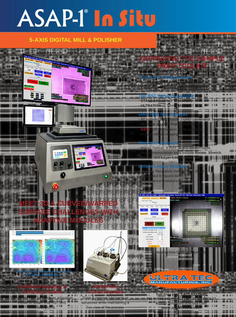
Toll Free (US) 1-877-542-0609Tel: 1-714-542-0608 Fax: 1-714-542-0627
e-mail: [email protected]
EXPANDING THE SAMPLE PREP TOOLKIT
‘In Situ’ RST Measurement- Single footprint system solution- Eliminates tilt/curve translation errors
Two RST Versions available- STANDARD NIR- ULTRATHIN
Ultra-High Res CamerasTarget,
45° Side 45° Front- NEW
Work with Overlays
Rotate, Stretch, Resize Layer-Locking
Unique Legacy Modules
5-AXIS DIGITAL MILL & POLISHER
MEET 3D & CURVED/WARPEDSURFACE CHALLENGES WITH
ADAPTIVE MODULES
Combined Mapping & Polishing Control
NEW Fluid Control System
Interactive Overlay Controls
ASAP-1-InSitu.indd 1 06/21/21 7:00 PM
SIEMENS DIGITAL INDUSTRIES SOFTWARE
Siemens EDA Where IC design and verification innovation meets tomorrow.
Siemens EDA helps you engineer a smarter future faster by addressing your technology, design, and system-level scaling challenges. siemens.com/eda