Embed Size (px)
Citation preview
LM5166 LM5166LM5166
MSP430FR5969
ADC
IO-LinkStack
L+
C/Q
L-
R G B
PWMPWMPWM
ADC
ADC
I2C
GPIO
3.9 to 4.1 V2.7 to 2.9 V 3.9 to 4.1 V
HDC1080
OPT3001
IO-Link
TIOL111 LEDDriver
TLC5971
RGB LED
Matrix
GND
Copyright © 2017, Texas Instruments Incorporated
1TIDUD35–September 2017Submit Documentation Feedback
Copyright © 2017, Texas Instruments Incorporated
RGB Signal Light With IO-Link Interface Reference Design
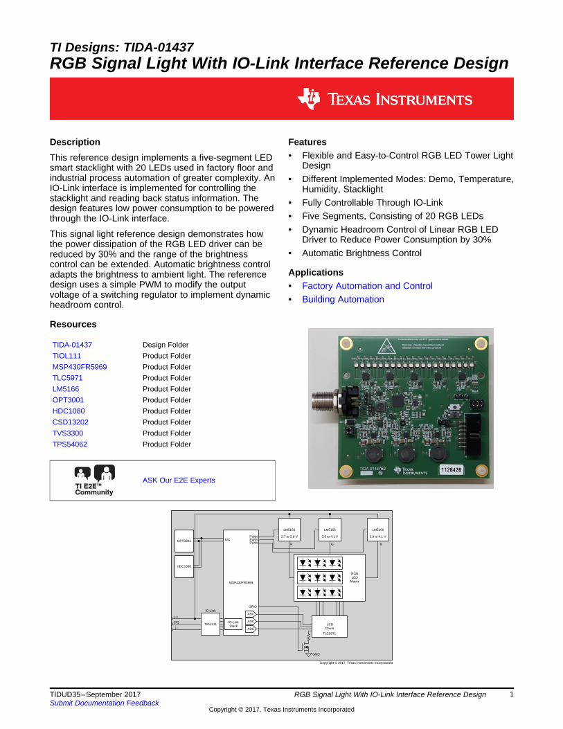
TI Designs: TIDA-01437RGB Signal Light With IO-Link Interface Reference Design
DescriptionThis reference design implements a five-segment LEDsmart stacklight with 20 LEDs used in factory floor andindustrial process automation of greater complexity. AnIO-Link interface is implemented for controlling thestacklight and reading back status information. Thedesign features low power consumption to be poweredthrough the IO-Link interface.
This signal light reference design demonstrates howthe power dissipation of the RGB LED driver can bereduced by 30% and the range of the brightnesscontrol can be extended. Automatic brightness controladapts the brightness to ambient light. The referencedesign uses a simple PWM to modify the outputvoltage of a switching regulator to implement dynamicheadroom control.
Resources
TIDA-01437 Design FolderTIOL111 Product FolderMSP430FR5969 Product FolderTLC5971 Product FolderLM5166 Product FolderOPT3001 Product FolderHDC1080 Product FolderCSD13202 Product FolderTVS3300 Product FolderTPS54062 Product Folder
ASK Our E2E Experts
Features• Flexible and Easy-to-Control RGB LED Tower Light
Design• Different Implemented Modes: Demo, Temperature,
Humidity, Stacklight• Fully Controllable Through IO-Link• Five Segments, Consisting of 20 RGB LEDs• Dynamic Headroom Control of Linear RGB LED
Driver to Reduce Power Consumption by 30%• Automatic Brightness Control
Applications• Factory Automation and Control• Building Automation
System Description www.ti.com
2 TIDUD35–September 2017Submit Documentation Feedback
Copyright © 2017, Texas Instruments Incorporated
RGB Signal Light With IO-Link Interface Reference Design
An IMPORTANT NOTICE at the end of this TI reference design addresses authorized use, intellectual property matters and otherimportant disclaimers and information.
1 System DescriptionIndustrial signal lights indicate the status of manufacturing equipment or the status of processes inindustrial environments. These lights are often called stacklights, tower lights, or indicator lights andcontain one to five difference colors. The IEC 60073 standard shows how the colors correspond todifferent states (see Table 1).
Table 1. IEC 60073 International Color Usage
COLOR SAFETY MEANING CONDITION OF PROCESSRed Danger Emergency or fault
Amber Warning AbnormalGreen Safe NormalBlue Mandatory significanceWhite No specific meaning assigned
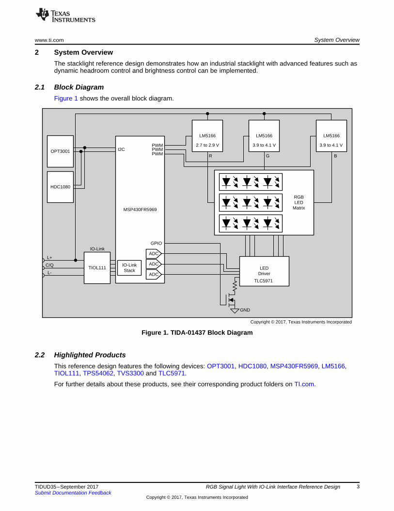
This reference design provides a universal stacklight option based on RGB LEDs. This option consists ofone PCB implementing the whole design as shown in Figure 1.
The design consists of four major parts:• Buck regulator for LED drivers with adjustable output voltage• LED drivers with configurable current• IO-Link interface and MSP430FR5969 microcontroller• Light sensor (OPT3001) and temperature and humidity sensor (HDC1080)
To power and control the design, only IO-Link is necessary. Each of the 20 RGB LEDs can be controlledindividually. To keep the power dissipation low, the supply voltage for the different color LEDs is regulatedfor each color and can be controlled depending on the selected brightness.
The design can be configured to:• Be a simple one-color stacklight• Be a programmable multi color stacklight• Be level or temperature light• Adapt the LED brightness depending on the ambient light
1.1 Key System Specifications
Table 2. Key System Specifications
PARAMETER SPECIFICATIONS
Input voltageVIN(min) = 20 VVIN(typ) = 24 VVIN(max) = 36 V
Current consumption at 24 V
ILEDs(off) = 0.1 mAILEDs(2 mA) = 30 mAILEDs(20 mA) = 280 mAILEDs(20 mA no DHC) = 190 mA
InterfacesIO-Link through Standard M12 ConnectorJTAG
LEDs 20 RGB LEDs, up to 20 mA each
LM5166 LM5166LM5166
MSP430FR5969
ADC
IO-LinkStack
L+
C/Q
L-
R G B
PWMPWMPWM
ADC
ADC
I2C
GPIO
3.9 to 4.1 V2.7 to 2.9 V 3.9 to 4.1 V
HDC1080
OPT3001
IO-Link
TIOL111 LEDDriver
TLC5971
RGB LED
Matrix
GND
Copyright © 2017, Texas Instruments Incorporated
www.ti.com System Overview
3TIDUD35–September 2017Submit Documentation Feedback
Copyright © 2017, Texas Instruments Incorporated
RGB Signal Light With IO-Link Interface Reference Design
2 System OverviewThe stacklight reference design demonstrates how an industrial stacklight with advanced features such asdynamic headroom control and brightness control can be implemented.
2.1 Block DiagramFigure 1 shows the overall block diagram.
Figure 1. TIDA-01437 Block Diagram
2.2 Highlighted ProductsThis reference design features the following devices: OPT3001, HDC1080, MSP430FR5969, LM5166,TIOL111, TPS54062, TVS3300 and TLC5971.
For further details about these products, see their corresponding product folders on TI.com.
SCL
SDA
ADDR
VDD
OPT3001
INTAmbient
Light
GND
I2C
Interface
VDD
ADCOptical
Filter
Copyright © 2017, Texas Instruments Incorporated
System Overview www.ti.com
4 TIDUD35–September 2017Submit Documentation Feedback
Copyright © 2017, Texas Instruments Incorporated
RGB Signal Light With IO-Link Interface Reference Design
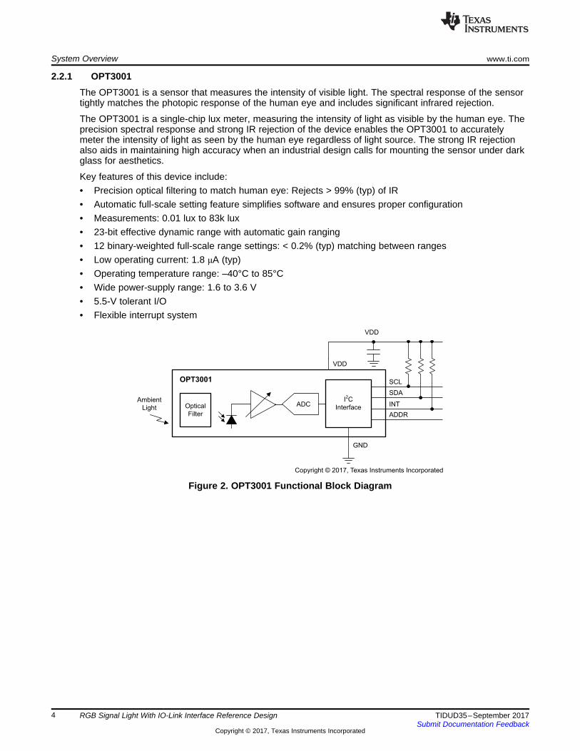
2.2.1 OPT3001The OPT3001 is a sensor that measures the intensity of visible light. The spectral response of the sensortightly matches the photopic response of the human eye and includes significant infrared rejection.
The OPT3001 is a single-chip lux meter, measuring the intensity of light as visible by the human eye. Theprecision spectral response and strong IR rejection of the device enables the OPT3001 to accuratelymeter the intensity of light as seen by the human eye regardless of light source. The strong IR rejectionalso aids in maintaining high accuracy when an industrial design calls for mounting the sensor under darkglass for aesthetics.
Key features of this device include:• Precision optical filtering to match human eye: Rejects > 99% (typ) of IR• Automatic full-scale setting feature simplifies software and ensures proper configuration• Measurements: 0.01 lux to 83k lux• 23-bit effective dynamic range with automatic gain ranging• 12 binary-weighted full-scale range settings: < 0.2% (typ) matching between ranges• Low operating current: 1.8 μA (typ)• Operating temperature range: –40°C to 85°C• Wide power-supply range: 1.6 to 3.6 V• 5.5-V tolerant I/O• Flexible interrupt system
Figure 2. OPT3001 Functional Block Diagram
ADC
TEMPERATURE
RH
I2C
Registers
+
Logic
HDC1080
SDASCL
OTP
Calibration Coefficients
VDD
GND
Copyright © 2017, Texas Instruments Incorporated
www.ti.com System Overview
5TIDUD35–September 2017Submit Documentation Feedback
Copyright © 2017, Texas Instruments Incorporated
RGB Signal Light With IO-Link Interface Reference Design
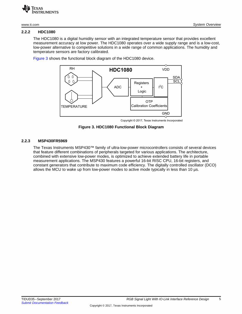
2.2.2 HDC1080The HDC1080 is a digital humidity sensor with an integrated temperature sensor that provides excellentmeasurement accuracy at low power. The HDC1080 operates over a wide supply range and is a low-cost,low-power alternative to competitive solutions in a wide range of common applications. The humidity andtemperature sensors are factory calibrated.
Figure 3 shows the functional block diagram of the HDC1080 device.
Figure 3. HDC1080 Functional Block Diagram
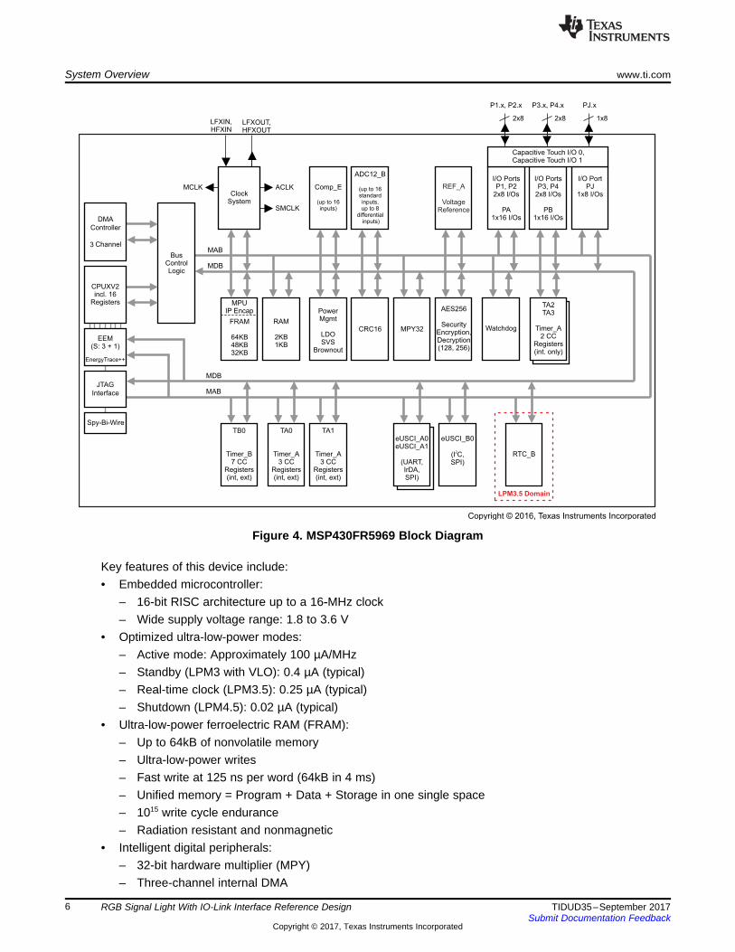
2.2.3 MSP430FR5969The Texas Instruments MSP430™ family of ultra-low-power microcontrollers consists of several devicesthat feature different combinations of peripherals targeted for various applications. The architecture,combined with extensive low-power modes, is optimized to achieve extended battery life in portablemeasurement applications. The MSP430 features a powerful 16-bit RISC CPU, 16-bit registers, andconstant generators that contribute to maximum code efficiency. The digitally controlled oscillator (DCO)allows the MCU to wake up from low-power modes to active mode typically in less than 10 µs.
EEM(S: 3 + 1)
Comp_E
(up to 16inputs)
FRAM
64KB48KB32KB
RAM
2KB1KB
PowerMgmt
LDOSVS
Brownout
SMCLK
ACLK
LFXOUT,HFXOUT
LFXIN,HFXIN
Spy-Bi-Wire
CRC16
BusControlLogic
MAB
MDB
MAB
MDB
MCLK
P1.x, P2.x
2x8
I/O PortPJ
1x8 I/Os
I/O PortsP3 4
2x8 I/Os
PB1x16 I/Os
, PI/O PortsP1, P2
2x8 I/Os
PA1x16 I/Os
P3.x, P4.x PJ.x
2 1x x8 8
MPY32
AES256
SecurityEnDecryption(128, 256)
cryption,
ADC12_B
(up to 16standardinputs,up to 8
differentialinputs)
ClockSystem
CPUXV2incl. 16
Registers
JTAG
Interface
DMA
Controller
3 Channel
Watchdog
REF_A
VoltageReference
MPUIP Encap
TB0
Timer_B7 CC
Registers(int, ext)
TA0
Timer_A3 CC
Registers(int, ext)
TA1
Timer_A3 CC
Registers(int, ext)
TA2TA3
Timer_A2 CC
Registers(int. only)
RTC_B
eUSCI_A0eUSCI_A1
(UART,IrDA,SPI)
eUSCI_B0
(I C,SPI)
2
Capacitive Touch I/O 0,1Capacitive Touch I/O
LPM3.5 Domain
EnergyTrace++
Copyright © 2016, Texas Instruments Incorporated
System Overview www.ti.com
6 TIDUD35–September 2017Submit Documentation Feedback
Copyright © 2017, Texas Instruments Incorporated
RGB Signal Light With IO-Link Interface Reference Design
Figure 4. MSP430FR5969 Block Diagram
Key features of this device include:• Embedded microcontroller:
– 16-bit RISC architecture up to a 16‑MHz clock– Wide supply voltage range: 1.8 to 3.6 V
• Optimized ultra-low-power modes:– Active mode: Approximately 100 µA/MHz– Standby (LPM3 with VLO): 0.4 µA (typical)– Real-time clock (LPM3.5): 0.25 µA (typical)– Shutdown (LPM4.5): 0.02 µA (typical)
• Ultra-low-power ferroelectric RAM (FRAM):– Up to 64kB of nonvolatile memory– Ultra-low-power writes– Fast write at 125 ns per word (64kB in 4 ms)– Unified memory = Program + Data + Storage in one single space– 1015 write cycle endurance– Radiation resistant and nonmagnetic
• Intelligent digital peripherals:– 32-bit hardware multiplier (MPY)– Three-channel internal DMA
www.ti.com System Overview
7TIDUD35–September 2017Submit Documentation Feedback
Copyright © 2017, Texas Instruments Incorporated
RGB Signal Light With IO-Link Interface Reference Design
– Real-time clock (RTC) with calendar and alarm functions– Five 16-bit timers with up to seven capture/compare registers each– 16-bit cyclic redundancy checker (CRC)
• High-performance analog:– 16-channel analog comparator– 12-bit analog-to-digital converter (ADC) with internal reference and sample-and-hold and up to 16
external input channels• Multifunction input/output ports:
– All pins support capacitive touch capability with no need for external components– Accessible bit-, byte-, and word-wise (in pairs)– Edge-selectable wake from LPM on all ports– Programmable pullup and pulldown on all ports
• Code security and encryption:– 128- or 256-bit AES security encryption and decryption coprocessor– Random number seed for random number generation algorithms
• Enhanced serial communication:– eUSCI_A0 and eUSCI_A1 support:
• UART with automatic baud-rate detection• IrDA encode and decode• SPI at rates up to 10 Mbps
– eUSCI_B0 supports:• I2C with multiple slave addressing• SPI at rates up to 8 Mbps
– Hardware UART and I2C bootstrap loader (BSL)• Flexible clock system:
– Fixed-frequency DCO with 10 selectable factory-trimmed frequencies– Low-power low-frequency internal clock source (VLO)– 32-kHz crystals (LFXT)– High-frequency crystals (HFXT)
For complete module descriptions, see the MSP430FR59xx user's guide.
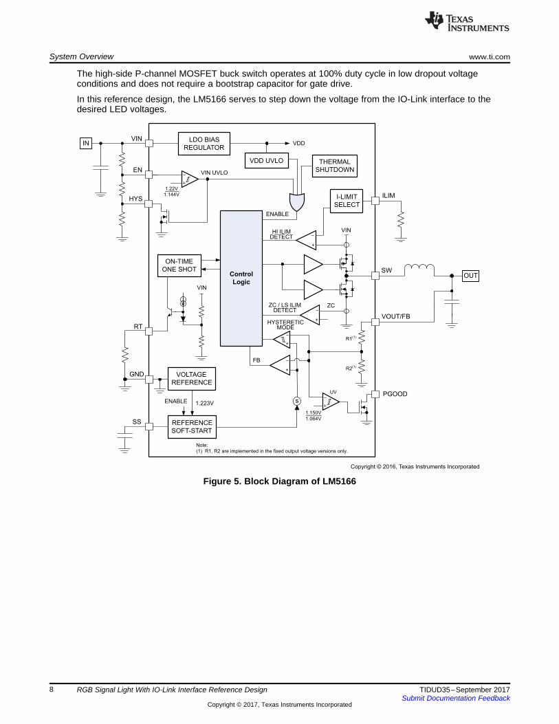
2.2.4 LM5166The LM5166 regulator is an easy-to-use synchronous buck DC/DC converter that operates from a 3- to65-V supply voltage. The device is intended for step-down conversions from 5-V, 12-V, 24-V, and 48-Vunregulated, semi-regulated and fully-regulated supply rails. With integrated high-side and low-side powerMOSFETs, the LM5166 delivers up to 500-mA DC load current with exceptional efficiency and ultra-lowinput quiescent current in a very small solution size.
Designed for simple implementation, a choice of operating modes offers flexibility to optimize its usageaccording to the target application. Fixed-frequency, constant on-time (COT) operation with discontinuousconduction mode (DCM) at light loads is ideal for low-noise, high-current, fast transient load requirements.Alternatively, pulse frequency modulation (PFM) mode achieves ultra-high, light-load efficiencyperformance. Control loop compensation is not required with either operating mode, reducing design timeand external component count.
The LM5166 incorporates other features for comprehensive system requirements, including an open-drainPower Good circuit for power-rail sequencing and fault reporting, internally-fixed or externally-adjustablesoft-start, monotonic startup into pre-biased loads, precision enable with customizable hysteresis forprogrammable line undervoltage lockout (UVLO), and thermal shutdown with automatic recovery. Thesefeatures enable a flexible and easy-to-use platform for a wide range of applications. The pin arrangementis designed for simple and optimized PCB layout, requiring only a few external components.
HI ILIMDETECT
VDD UVLO
ON-TIME
ONE SHOT
LDO BIAS
REGULATOR
VIN
FB
ENABLE
THERMAL
SHUTDOWNVIN UVLO
ZC / LS ILIMDETECT
VDD
ZC
I-LIMIT
SELECT
Control
LogicVIN
IN
OUT
HYSTERETICMODE
REFERENCE
SOFT-START
ENABLE
VOLTAGE
REFERENCE
1.223V
VIN
1.22V
1.144V
EN
HYSILIM
SW
RT
SS
GND
PGOOD
1.150V
1.064V
UV
+
+
+
s
Copyright © 2016, Texas Instruments Incorporated
VOUT/FB
R1(1)
R2(1)
Note:
(1) R1, R2 are implemented in the fixed output voltage versions only.
System Overview www.ti.com
8 TIDUD35–September 2017Submit Documentation Feedback
Copyright © 2017, Texas Instruments Incorporated
RGB Signal Light With IO-Link Interface Reference Design
The high-side P-channel MOSFET buck switch operates at 100% duty cycle in low dropout voltageconditions and does not require a bootstrap capacitor for gate drive.
In this reference design, the LM5166 serves to step down the voltage from the IO-Link interface to thedesired LED voltages.
Figure 5. Block Diagram of LM5166
ERROR
AMPLIFIER
Boot
Charge
Boot
UVLO
UVLO
Current
Sense
Oscillator
with PLL
Frequency
Shift
Deadtime
Control Logic
Slope
Compensation
PWM
Comparator
Minimum
Clamp
Maximum
Clamp
REFERENCE
DAC
VSENSE
COMP
RT CLK/
PH
BOOT
VIN
GND
Thermal
Shutdown
EN
Enable
Comparator
Shutdown
Logic
Shutdown
Enable
Threshold
Shutdown
OV
DRV
REG
ZX
detect
Copyright © 2016, Texas Instruments Incorporated
www.ti.com System Overview
9TIDUD35–September 2017Submit Documentation Feedback
Copyright © 2017, Texas Instruments Incorporated
RGB Signal Light With IO-Link Interface Reference Design
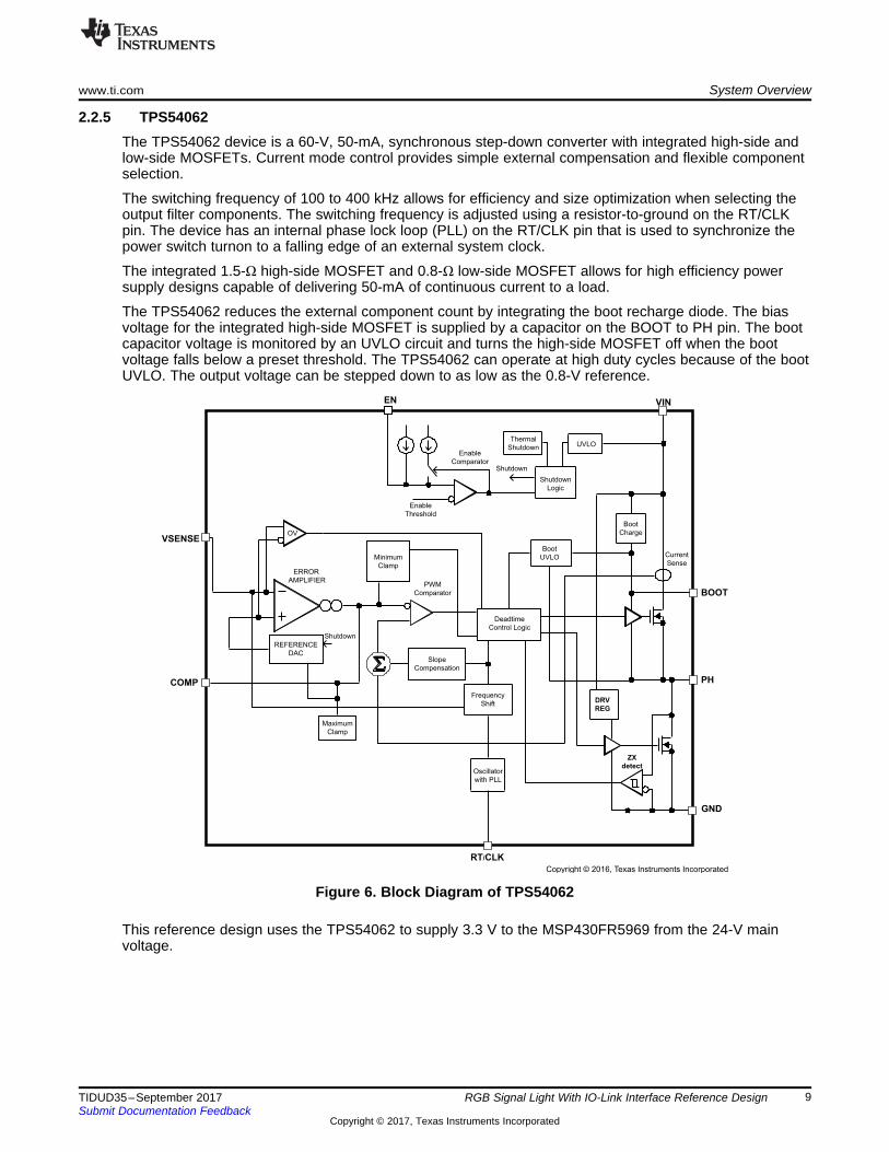
2.2.5 TPS54062The TPS54062 device is a 60-V, 50-mA, synchronous step-down converter with integrated high-side andlow-side MOSFETs. Current mode control provides simple external compensation and flexible componentselection.
The switching frequency of 100 to 400 kHz allows for efficiency and size optimization when selecting theoutput filter components. The switching frequency is adjusted using a resistor-to-ground on the RT/CLKpin. The device has an internal phase lock loop (PLL) on the RT/CLK pin that is used to synchronize thepower switch turnon to a falling edge of an external system clock.
The integrated 1.5-Ω high-side MOSFET and 0.8-Ω low-side MOSFET allows for high efficiency powersupply designs capable of delivering 50-mA of continuous current to a load.
The TPS54062 reduces the external component count by integrating the boot recharge diode. The biasvoltage for the integrated high-side MOSFET is supplied by a capacitor on the BOOT to PH pin. The bootcapacitor voltage is monitored by an UVLO circuit and turns the high-side MOSFET off when the bootvoltage falls below a preset threshold. The TPS54062 can operate at high duty cycles because of the bootUVLO. The output voltage can be stepped down to as low as the 0.8-V reference.
Figure 6. Block Diagram of TPS54062
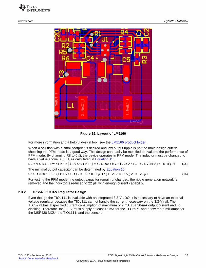
This reference design uses the TPS54062 to supply 3.3 V to the MSP430FR5969 from the 24-V mainvoltage.
Voltage Level
Detection
Power FET
Driver
IN
GND
Copyright © 2017, Texas Instruments Incorporated
System Overview www.ti.com
10 TIDUD35–September 2017Submit Documentation Feedback
Copyright © 2017, Texas Instruments Incorporated
RGB Signal Light With IO-Link Interface Reference Design
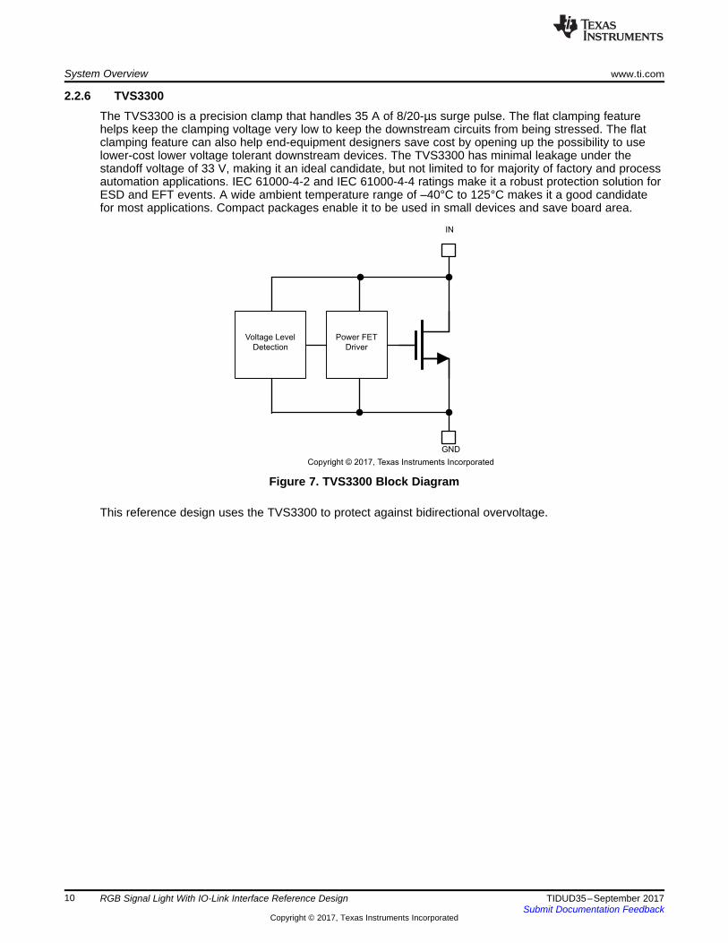
2.2.6 TVS3300The TVS3300 is a precision clamp that handles 35 A of 8/20-µs surge pulse. The flat clamping featurehelps keep the clamping voltage very low to keep the downstream circuits from being stressed. The flatclamping feature can also help end-equipment designers save cost by opening up the possibility to uselower-cost lower voltage tolerant downstream devices. The TVS3300 has minimal leakage under thestandoff voltage of 33 V, making it an ideal candidate, but not limited to for majority of factory and processautomation applications. IEC 61000-4-2 and IEC 61000-4-4 ratings make it a robust protection solution forESD and EFT events. A wide ambient temperature range of –40°C to 125°C makes it a good candidatefor most applications. Compact packages enable it to be used in small devices and save board area.
Figure 7. TVS3300 Block Diagram
This reference design uses the TVS3300 to protect against bidirectional overvoltage.
DIAGNOSTICS
and
CONTROL
CO
NT
RO
L
LO
GIC
ILIM_ADJ
CUR_OK
EN
TX
VCC_ IN
PWR_OK
L+
CQ
L-
TMP_OK
WAKE
RX
NFAULT
Copyright © 2017, Texas Instruments Incorporated
www.ti.com System Overview
11TIDUD35–September 2017Submit Documentation Feedback
Copyright © 2017, Texas Instruments Incorporated
RGB Signal Light With IO-Link Interface Reference Design
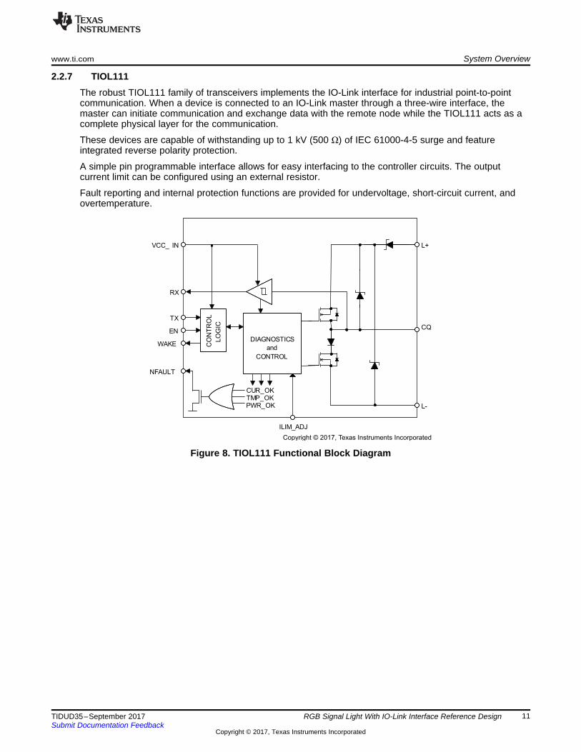
2.2.7 TIOL111The robust TIOL111 family of transceivers implements the IO-Link interface for industrial point-to-pointcommunication. When a device is connected to an IO-Link master through a three-wire interface, themaster can initiate communication and exchange data with the remote node while the TIOL111 acts as acomplete physical layer for the communication.
These devices are capable of withstanding up to 1 kV (500 Ω) of IEC 61000-4-5 surge and featureintegrated reverse polarity protection.
A simple pin programmable interface allows for easy interfacing to the controller circuits. The outputcurrent limit can be configured using an external resistor.
Fault reporting and internal protection functions are provided for undervoltage, short-circuit current, andovertemperature.
Figure 8. TIOL111 Functional Block Diagram
Write
Command
Decode
6
218
SDTO
Refe encer
Current
Control
SCKI
IREF
GND
224-Bit Shift Register
218-Bit Data Latch
GS Clock
Counter
SCKO
12-Channel Constant Sink Current Driver
with 7-Bit, 3-Grouped BC
3-Grouped Switching Delay
12
LSB MSB
0 223
LSB MSB
0 217
VCC
SDTI
OUTB3OUTG3OUTR3OUTB0OUTG0OUTR0
26
UVLO
21
Thermal
Detection
Clock
Timing
Adjust
3.3 V
REGVREG
Data
Latch
Control
reset
reset
Clock
Select
Internal
Oscillator16-Bit ES-PW Timing ControlM
intlat
1921 intlat
3
16
wrtena
EXTCLK
BLANK
TMGRST
BCX
GSX
BLANK
DSPRPT
OUTTMG
12
2
System Overview www.ti.com
12 TIDUD35–September 2017Submit Documentation Feedback
Copyright © 2017, Texas Instruments Incorporated
RGB Signal Light With IO-Link Interface Reference Design
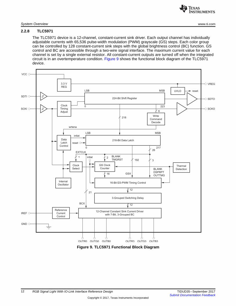
2.2.8 TLC5971The TLC5971 device is a 12-channel, constant-current sink driver. Each output channel has individuallyadjustable currents with 65,536 pulse-width modulation (PWM) grayscale (GS) steps. Each color groupcan be controlled by 128 constant-current sink steps with the global brightness control (BC) function. GScontrol and BC are accessible through a two-wire signal interface. The maximum current value for eachchannel is set by a single external resistor. All constant-current outputs are turned off when the integratedcircuit is in an overtemperature condition. Figure 9 shows the functional block diagram of the TLC5971device.
Figure 9. TLC5971 Functional Block Diagram
JTAG Connector
LED Stack Light
IO-Link Connector
LM5166 Red LM5166 Green LM5166 Blue
Testpoints forResidue voltage
TLC5971 LED Driver
IO-Link PHY
MSP430FR5969
OPT3001 and HDC1080
Copyright © 2017, Texas Instruments Incorporated
www.ti.com System Overview
13TIDUD35–September 2017Submit Documentation Feedback
Copyright © 2017, Texas Instruments Incorporated
RGB Signal Light With IO-Link Interface Reference Design
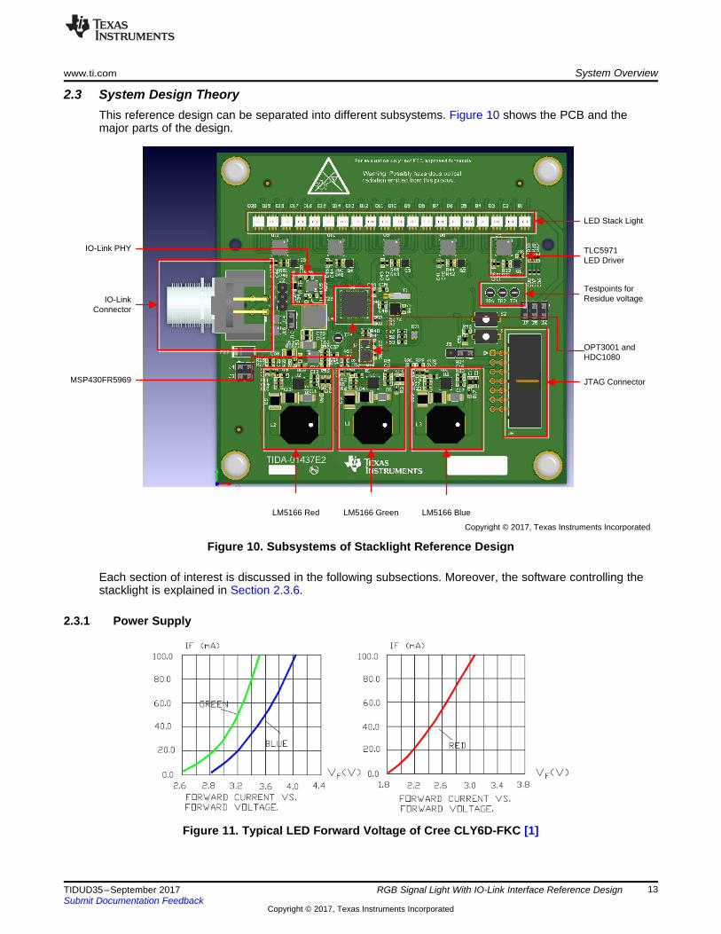
2.3 System Design TheoryThis reference design can be separated into different subsystems. Figure 10 shows the PCB and themajor parts of the design.
Figure 10. Subsystems of Stacklight Reference Design
Each section of interest is discussed in the following subsections. Moreover, the software controlling thestacklight is explained in Section 2.3.6.
2.3.1 Power Supply
Figure 11. Typical LED Forward Voltage of Cree CLY6D-FKC [1]
70
60
50
40
30
20
10
00 3
Output Voltage (V)
Outp
ut C
urr
ent (m
A)
0.5 1
I = 60 mAOLCMax I = 50 mAOLCMax
I = 40 mAOLCMax
I = 30 mAOLCMax
I = 20 mAOLCMax
I = 10 mAOLCMax
T = +25 C, VCC = 12 V, BCx = 7Fh°A
I = 5 mAOLCMaxI = 2 mAOLCMax
1.5 2.52
System Overview www.ti.com
14 TIDUD35–September 2017Submit Documentation Feedback
Copyright © 2017, Texas Instruments Incorporated
RGB Signal Light With IO-Link Interface Reference Design
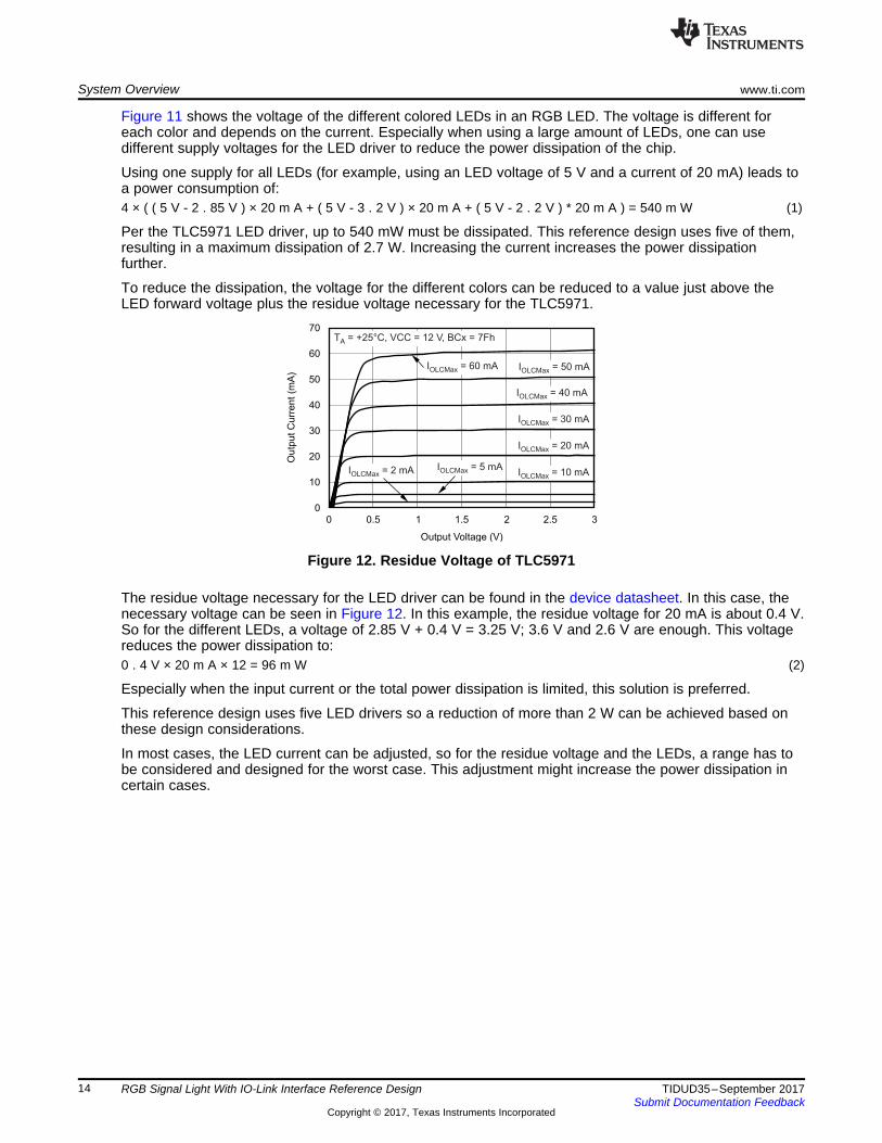
Figure 11 shows the voltage of the different colored LEDs in an RGB LED. The voltage is different foreach color and depends on the current. Especially when using a large amount of LEDs, one can usedifferent supply voltages for the LED driver to reduce the power dissipation of the chip.
Using one supply for all LEDs (for example, using an LED voltage of 5 V and a current of 20 mA) leads toa power consumption of:4 × ( ( 5 V - 2 . 85 V ) × 20 m A + ( 5 V - 3 . 2 V ) × 20 m A + ( 5 V - 2 . 2 V ) * 20 m A ) = 540 m W (1)
Per the TLC5971 LED driver, up to 540 mW must be dissipated. This reference design uses five of them,resulting in a maximum dissipation of 2.7 W. Increasing the current increases the power dissipationfurther.
To reduce the dissipation, the voltage for the different colors can be reduced to a value just above theLED forward voltage plus the residue voltage necessary for the TLC5971.
Figure 12. Residue Voltage of TLC5971
The residue voltage necessary for the LED driver can be found in the device datasheet. In this case, thenecessary voltage can be seen in Figure 12. In this example, the residue voltage for 20 mA is about 0.4 V.So for the different LEDs, a voltage of 2.85 V + 0.4 V = 3.25 V; 3.6 V and 2.6 V are enough. This voltagereduces the power dissipation to:0 . 4 V × 20 m A × 12 = 96 m W (2)
Especially when the input current or the total power dissipation is limited, this solution is preferred.
This reference design uses five LED drivers so a reduction of more than 2 W can be achieved based onthese design considerations.
In most cases, the LED current can be adjusted, so for the residue voltage and the LEDs, a range has tobe considered and designed for the worst case. This adjustment might increase the power dissipation incertain cases.
57.6kR2
47µFC4
0 - 3.3V
100kR7
100kR1
1.0k
R10
1.0k
R13
GND GND
PWM 20kHz 3.3V
-44dB@20kHz
TB0.4
0.1µFC19
0.1µFC20
Vgreen
12
J5
SH-J510µFC3
100µH
L1
Copyright © 2017, Texas Instruments Incorporated
SW 1VIN2
ILIM 3
SS4
RT5
PGOOD6
EN7
VOUT/FB8
HYS9
GND10
PAD11
U1
LM5166DRCR
2.2µFC5
100µH
L1
57.6kR2
768k
R3
100pFC2
0.01µF
C6
GND
158kR8
47µFC4
1.00MR4
64.9k
R5
10.0kR6
+24V
100kR1
Vgreen
12
J5
SH-J5
1000pF
C1
10µFC3
GND
Copyright © 2017, Texas Instruments Incorporated
www.ti.com System Overview
15TIDUD35–September 2017Submit Documentation Feedback
Copyright © 2017, Texas Instruments Incorporated
RGB Signal Light With IO-Link Interface Reference Design
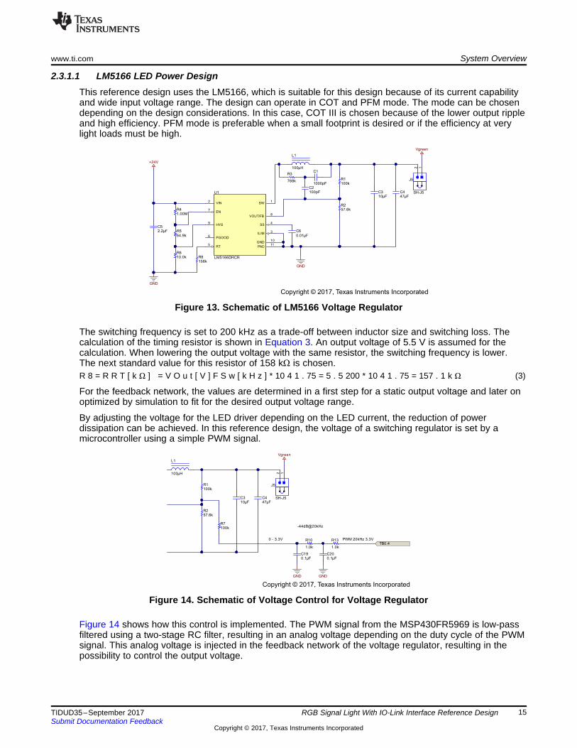
2.3.1.1 LM5166 LED Power DesignThis reference design uses the LM5166, which is suitable for this design because of its current capabilityand wide input voltage range. The design can operate in COT and PFM mode. The mode can be chosendepending on the design considerations. In this case, COT III is chosen because of the lower output rippleand high efficiency. PFM mode is preferable when a small footprint is desired or if the efficiency at verylight loads must be high.
Figure 13. Schematic of LM5166 Voltage Regulator
The switching frequency is set to 200 kHz as a trade-off between inductor size and switching loss. Thecalculation of the timing resistor is shown in Equation 3. An output voltage of 5.5 V is assumed for thecalculation. When lowering the output voltage with the same resistor, the switching frequency is lower.The next standard value for this resistor of 158 kΩ is chosen.R 8 = R R T [ k Ω ] = V O u t [ V ] F S w [ k H z ] * 10 4 1 . 75 = 5 . 5 200 * 10 4 1 . 75 = 157 . 1 k Ω (3)
For the feedback network, the values are determined in a first step for a static output voltage and later onoptimized by simulation to fit for the desired output voltage range.
By adjusting the voltage for the LED driver depending on the LED current, the reduction of powerdissipation can be achieved. In this reference design, the voltage of a switching regulator is set by amicrocontroller using a simple PWM signal.
Figure 14. Schematic of Voltage Control for Voltage Regulator
Figure 14 shows how this control is implemented. The PWM signal from the MSP430FR5969 is low-passfiltered using a two-stage RC filter, resulting in an analog voltage depending on the duty cycle of the PWMsignal. This analog voltage is injected in the feedback network of the voltage regulator, resulting in thepossibility to control the output voltage.
System Overview www.ti.com
16 TIDUD35–September 2017Submit Documentation Feedback
Copyright © 2017, Texas Instruments Incorporated
RGB Signal Light With IO-Link Interface Reference Design
For this reference design, this circuit is built three times to control the voltage of each color. Thecalculation of the feedback network is shown in Equation 4 to Equation 7.R 12 = R 1 × R 2 R 1 + R 2 = 100 k Ω * 57 . 6 k Ω 100 k Ω + 57 . 6 k Ω = 36 . 55 k Ω (4)R 27 = R 2 × R 7 R 2 + R 7 = 100 k Ω * 57 . 6 k Ω 100 k Ω + 57 . 6 k Ω = 36 . 55 k Ω (5)V m i n = ( U f b - R 12 × V P W M R 12 + R 7 ) * ( R 12 + R 1 ) R 72 = ( 1 . 223 V - 36 . 55 k Ω * 3 . 3 V 36 . 55 k Ω +100 k Ω ) * ( 36 . 55 k Ω + 100 k Ω ) 36 . 55 k Ω = 1 . 3 V (6)V m a x = U f b × ( R 12 + R 1 ) R 27 = 1 . 223 V * ( 36 . 55 k Ω + 100 k Ω ) 36 . 55 k Ω = 4 . 6 V (7)
More accurate values can be achieved by simulation because the RC filter as well as the outputresistance of the MSP430 is neglected in this calculation.
The type-3 ripple generation method uses the voltage on the switch node to inject a ripple voltage to thefeedback node. Because it does not use the output voltage to generate ripple, it is suited for applicationswhere a low ripple is desired. Equation 8 to Equation 12 show how the margins of the ripple injectionnetwork can be calculated.C 1 = C A ≥ 5 F S w × ( R 1 | | R 2 ) = 5 200 k H z * 36 . 55 k Ω = 0 . 68 n F (8)C 2 = C B ≥ 1 2 π × F S w × ( R 1 | | R 2 ) = 1 2 π * 200 k H z * 36 . 66 k Ω = 22 p F (9)T o n = V O u t V I n × F S w = 5 . 5 V 36 V * 200 k H z = 0 . 76 μ s (10)R 3 × C 1 = R A × C A ≤ ( V I n - V O u t ) * T O n 20 m V = ( 36 V - 5 . 5 V ) * 0 . 76 μ s 20 m V = 1 . 159 * 10 - 3
(11)R 3 = R A ≤ 1 . 159 × 10 - 3 C A = 1 . 159 * 10 - 3 0 . 68 n F = 1 . 7 M Ω (12)
For further information on how to design the ripple generation network, see the application reportSelecting an Ideal Ripple Generation Network for Your COT Buck Converter.
The next step is to calculate an inductor value; to do so, the inductor ripple current must be defined.Typically, this current is chosen to be between 30% and 60%. In this case, it is selected to be 40% of themaximum output current, resulting in 200 mA. The calculation is shown in Equation 13. The selectedinductor value is 100 µH.L 1 = L F = V O u t F S w × Δ I L × ( 1 - V O u t V I n ) = 5 . 5 200 k H z * ( 40 % * 500 m A ) * ( 1 - 5 . 5 V 24 V ) =106 μ H (13)
The minimum output capacitance depends on the desired output voltage ripple. In this case, a ripple of 10mV is defined for calculations. Equation 14 shows the way the capacitance is calculated.C O u t ≥ Δ I L 8 × F S w × Δ V O u t = 200 m A 8 * 200 k H z * 10 m V = 12 . 5 μ F (14)
This reference design uses capacitors at 10 µF and 47 µF in parallel. Look at the voltage derating of thecapacitor to know the capacitance at the applied voltage. As a result, a voltage rating of 25 V for the 10-µF capacitor is chosen. It is placed as close as possible to the LM5166 and the input capacitor. The 47-µFcapacitor is not that critical and is chosen to be a 10-V type. All capacitors have X7R dielectricum.
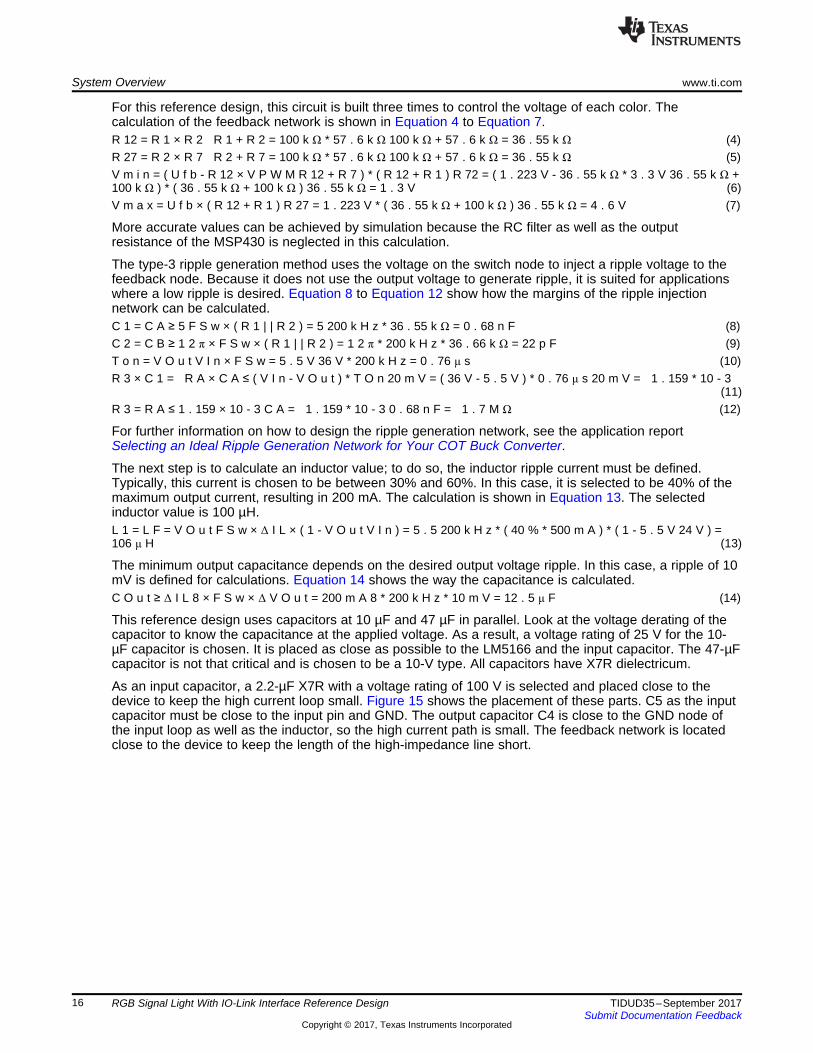
As an input capacitor, a 2.2-µF X7R with a voltage rating of 100 V is selected and placed close to thedevice to keep the high current loop small. Figure 15 shows the placement of these parts. C5 as the inputcapacitor must be close to the input pin and GND. The output capacitor C4 is close to the GND node ofthe input loop as well as the inductor, so the high current path is small. The feedback network is locatedclose to the device to keep the length of the high-impedance line short.
www.ti.com System Overview
17TIDUD35–September 2017Submit Documentation Feedback
Copyright © 2017, Texas Instruments Incorporated
RGB Signal Light With IO-Link Interface Reference Design
Figure 15. Layout of LM5166
For more information and a helpful design tool, see the LM5166 product folder.
When a solution with a small footprint is desired and low output ripple is not the main design criteria,choosing the PFM mode is a good way. This design can easily be modified to evaluate the performance ofPFM mode. By changing R8 to 0 Ω, the device operates in PFM mode. The inductor must be changed tohave a value above 8.5 µH, as calculated in Equation 15.L 1 = V O u t F S w × I P k × ( 1 - V O u t V I n ) = 5 . 5 400 k H z * 1 . 25 A * ( 1 - 5 . 5 V 24 V ) = 8 . 5 μ H (15)
The minimal output capacitor can be determined by Equation 16.C O u t ≥ 50 × L 1 × ( I P k V O u t ) 2 = 50 * 8 . 5 μ H * ( 1 . 25 A 5 . 5 V ) 2 = 22 μ F (16)
For testing the PFM mode, the output capacitor remain unchanged, the ripple generation network isremoved and the inductor is reduced to 22 µH with enough current capability.
2.3.2 TPS54062 3.3-V Regulator DesignEven though the TIOL111 is available with an integrated 3.3-V LDO, it is necessary to have an externalvoltage regulator because the TIOL111 cannot handle the current necessary on the 3.3-V rail. TheTLC5971 has a specified current consumption of maximum of 9 mA at a 30-mA output current and noclocking. Therefore. the 3.3 V must supply at least 45 mA for the TLC5971 and a few more milliamps forthe MSP430 MCU, the TIOL111, and the sensors.
BOOT1
VIN2
EN3
RT/CLK4
VSENSE5
COMP6
GND7
PH8
TP9
U13
TPS54062DRBT
220µH
L4
0.01µFC52
GND
2.2µFC53
10µFC54
10µFC55
113kR59
357kR55
25.5kR58 20.5k
R57
0.01µFC57
33pFC56
GND
30.9kR54
10.0kR56
3V3+24V
1
2
J4 SH-J4
1
2
J10 SH-J10
0.1µFC58
Copyright © 2017, Texas Instruments Incorporated
System Overview www.ti.com
18 TIDUD35–September 2017Submit Documentation Feedback
Copyright © 2017, Texas Instruments Incorporated
RGB Signal Light With IO-Link Interface Reference Design
Figure 16. 3.3-V Regulation From 24 V
The parts of the TPS54062 regulator are calculated by using the calculator tool in the TPS54062 productfolder.
To keep the output ripple on the 3.3 V low, an inductor value larger than the calculated value (220 µHinstead of 150 µH) and a larger output capacitor are used.
2.3.3 LED DriverThere are many solutions for controlling LEDs. The LED requires a constant current. The variety ofavailable LEDs is large, and the brightness is usually dependent on the current that is going through theLED.
In this reference design, the 12-channel RGB LED driver (TLC5971) controls the LEDs and provides thefollowing advantages:• Dedicated RGB LED controller• Twelve independent constant-current sinks to adjust to the current for each channel• Ability to use the driver with different types of LEDs with up to 60 mA for each channel• Simple two-wire interface to control the TLC5971 from an MCU• Several devices can be daisy-chained
Figure 17 shows the schematic of one LED driver. Typically, the LED driver is powered through the VCCpin with a voltage of minimum 6 V and delivers a regulated 3.3 V at the VREG output. When the devicemust operate below 6 V and the internal regulator is not used, VCC and VREG must be tied together tothe desired voltage.
The maximum output current of the LED driver is set by a resistor at the IREF pin to GND. Additionally, aninternal 7-bit wide register is used for a global brightness control, allowing a reduction of the current downto 1/127th of the programmed maximum current. When high-brightness LEDs are used or a high LEDcurrent is set, even the lowest current might be too bright in some circumstances. In this case, the currentcan be programmed to a low value, and a second resistor switched with a MOSFET can be connected inparallel when high current is necessary.

SDTI1
SCKI2
NC3
NC4
SCKO5
SDTO6
OUTR27
OUTG28
OUTB29
OUTR310
OUTG311
OUTB312
VCC13
NC14
VREG15
IREF16
NC17
GND18
OUTR019
OUTG020
OUTB021
OUTR122
OUTG123
OUTB124
GND25
U4
TLC5971RGER
3V3
1µFC25
GND
0.1µFC26
GNDGND
2.7kR31
GND
10kR33
GND
CUR_SET
2.2mA / 20.6mA FS
UCA0_CLK
UCA0_SIMO
GND
22kR32
1µFC36
1.0kR37
1µFC37
1.0kR38
1µFC38
1.0kR39
GND GND GND
A14A13A12
G6
5
4
1
2
3
R
B
Rgb
D1
CLY6D-FKC-CK1N1D1BB7D3D3
G6
5
4
1
2
3
R
B
Rgb
D2
CLY6D-FKC-CK1N1D1BB7D3D3
G6
5
4
1
2
3
R
B
Rgb
D3
CLY6D-FKC-CK1N1D1BB7D3D3
G6
5
4
1
2
3
R
B
Rgb
D4
CLY6D-FKC-CK1N1D1BB7D3D3
Vred
Vgreen
Vblue
LED1_CLKO
LED1_SDO
3
5,6
,84
,71
,2, Q1
CSD13202Q2
TP1 TP2 TP3
Copyright © 2017, Texas Instruments Incorporated
www.ti.com System Overview
19TIDUD35–September 2017Submit Documentation Feedback
Copyright © 2017, Texas Instruments Incorporated
RGB Signal Light With IO-Link Interface Reference Design
Figure 17. Schematic of LED Driver With Voltage Measurement
The brightness control is usually 7 bits wide and controls the current in 1/127 × ISET steps. To set themaximum current, the IREF pin of the TLC5971 is connected through a resistor to GND. When configuringthe TLC5971 for higher current, a 2.7-kΩ resistor in parallel with 22 kΩ is used. This results in 2.4 kΩequaling a 20.6-mA maximum current and 0.16 mA per step. Depending on the number of LEDs used,even this low current is still too bright.
To resolve this, a low-power mode is default with about a 2-mA maximum current and the MSP430 has toconnect a second resistor in parallel to increase the current. By doing this, it is possible to go down to0.016 mA but still be able to increase to up to 20 mA.
To get feedback about the residue voltage, the three outputs of one channel are connected to themicrocontroller through a simple RC low-pass filter.
In an separate mode, the residue voltage is measured and the LED voltage is regulated to the minimalpossible value for the given current. This process is done for multiple currents and stored. During runtime,these values are used. Whenever the LED with voltage monitoring is turned on, the PWM value for thecorresponding channel is reduced or increased, depending on the measured voltage drop.
VDD1
ADDR2
GND3
SCL4
INT5
SDA6
PAD7
U7
OPT3001DNPR
UCB0SCLUCB0SDA
GND
3V3 3V3 3V3
GND
SDA1
GND2
NC3
NC4
VDD5
SCL6
PAD7
U12
HDC1080DMBR
3V3
GND
UCB0SCLUCB0SDA
GND
I2C: 0x40 I2C: 0x44
0.1µFC39
0.1µFC50
1.0kR40
1.0kR41
Copyright © 2017, Texas Instruments Incorporated
VCC_IN/OUT1
FAULT2
RX3
TX4
EN5
LIM_ADJ6
GND11
CQ8
L+9
L-7
WAKE10
U5
TIOL111
41
32
J143-01205
A1RX
A1TX
EN
WAKE
FAULT
GND
1µFC28
0
R36GND
1 2 3
J2
3V3
10kR35
10kR34
+24V
150pFC27
150pFC30
1µFC29
IN4
IN5
GN
D1
GN
D2
IN6
GN
D3
PA
D7
U14TVS3300DRVR
IN4
IN5
GN
D1
GN
D2
IN6
GN
D3
PA
D7
U15TVS3300DRVR
D22B160-13-F
Copyright © 2017, Texas Instruments Incorporated
System Overview www.ti.com
20 TIDUD35–September 2017Submit Documentation Feedback
Copyright © 2017, Texas Instruments Incorporated
RGB Signal Light With IO-Link Interface Reference Design
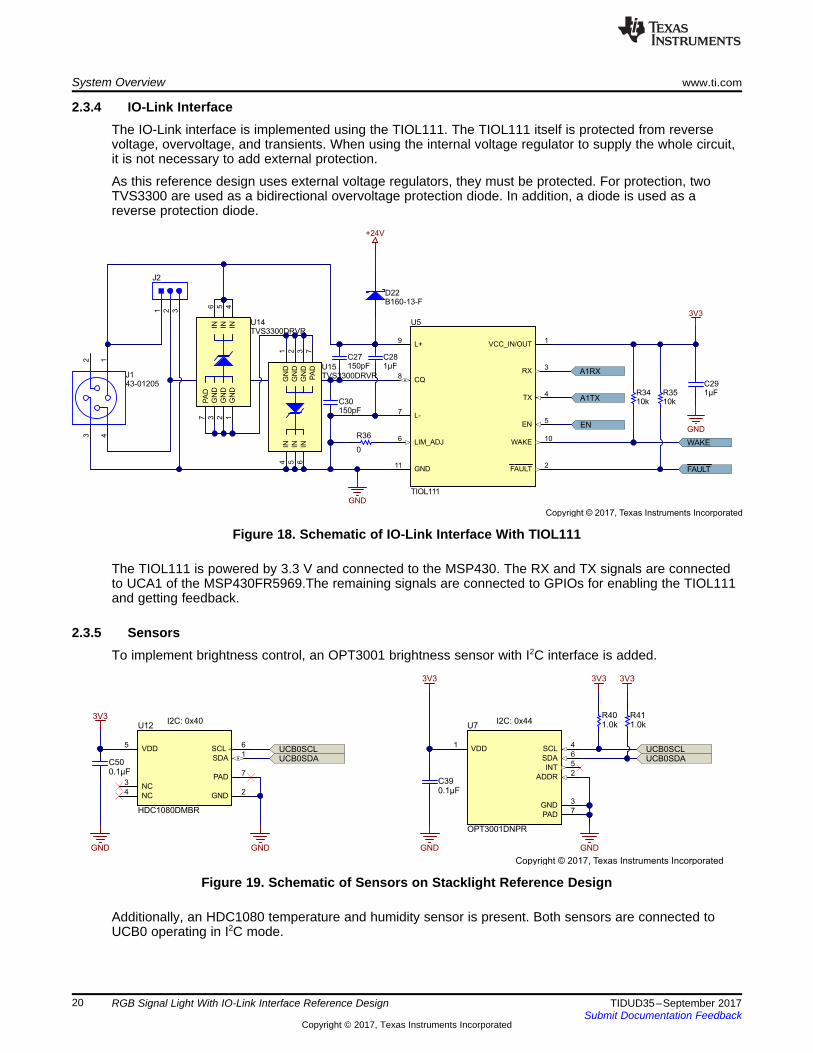
2.3.4 IO-Link InterfaceThe IO-Link interface is implemented using the TIOL111. The TIOL111 itself is protected from reversevoltage, overvoltage, and transients. When using the internal voltage regulator to supply the whole circuit,it is not necessary to add external protection.
As this reference design uses external voltage regulators, they must be protected. For protection, twoTVS3300 are used as a bidirectional overvoltage protection diode. In addition, a diode is used as areverse protection diode.
Figure 18. Schematic of IO-Link Interface With TIOL111
The TIOL111 is powered by 3.3 V and connected to the MSP430. The RX and TX signals are connectedto UCA1 of the MSP430FR5969.The remaining signals are connected to GPIOs for enabling the TIOL111and getting feedback.
2.3.5 SensorsTo implement brightness control, an OPT3001 brightness sensor with I2C interface is added.
Figure 19. Schematic of Sensors on Stacklight Reference Design
Additionally, an HDC1080 temperature and humidity sensor is present. Both sensors are connected toUCB0 operating in I2C mode.
www.ti.com System Overview
21TIDUD35–September 2017Submit Documentation Feedback
Copyright © 2017, Texas Instruments Incorporated
RGB Signal Light With IO-Link Interface Reference Design
2.3.6 Firmware ImplementationThis reference design includes a firmware implementing an IO-Link stack, the control of the LED drivers,and the controller for the adjustable buck regulator.
2.3.6.1 IO-Link CommunicationThe IO-Link stack is developed by TE Concept. It is not part of this design and not explained in detail.
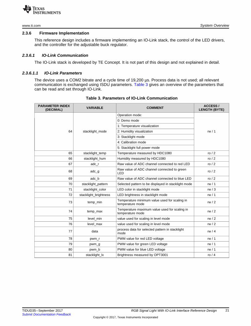
2.3.6.1.1 IO-Link ParametersThe device uses a COM2 bitrate and a cycle time of 19,200 µs. Process data is not used; all relevantcommunication is exchanged using ISDU parameters. Table 3 gives an overview of the parameters thatcan be read and set through IO-Link.
Table 3. Parameters of IO-Link Communication
PARAMETER INDEX(DECIMAL) VARIABLE COMMENT ACCESS /
LENGTH (BYTE)
64 stacklight_mode
Operation mode:
rw / 1
0: Demo mode1: Temperature visualization2: Humidity visualization3: Stacklight mode4: Calibration mode5: Stacklight full power mode
65 stacklight_temp Temperature measured by HDC1080 ro / 266 stacklight_hum Humidity measured by HDC1080 ro / 267 adc_r Raw value of ADC channel connected to red LED ro / 2
68 adc_g Raw value of ADC channel connected to greenLED ro / 2
69 adc_b Raw value of ADC channel connected to blue LED ro / 270 stacklight_pattern Selected pattern to be displayed in stacklight mode rw / 171 stacklight_color LED color in stacklight mode rw / 372 stacklight_brightness LED brightness in stacklight mode rw / 1
73 temp_min Temperature minimum value used for scaling intemperature mode rw / 2
74 temp_max Temperature maximum value used for scaling intemperature mode rw / 2
75 level_min value used for scaling in level mode rw / 276 level_max value used for scaling in level mode rw / 2
77 data process data for selected pattern in stacklightmode rw / 4
78 pwm_r PWM value for red LED voltage rw / 179 pwm_g PWM value for green LED voltage rw / 180 pwm_b PWM value for blue LED voltage rw / 181 stacklight_lx Brightness measured by OPT3001 ro / 4
System Overview www.ti.com
22 TIDUD35–September 2017Submit Documentation Feedback
Copyright © 2017, Texas Instruments Incorporated
RGB Signal Light With IO-Link Interface Reference Design
The usage of the data parameter (77) depends on the selected pattern (parameter 70). These values areonly used when mode (64) is set to 3 or 5. Table 4 explains the usage of the data parameter in that case.
Table 4. Data Parameter
PATTERNVALUE PATTERN DATA PARAMETER
0 On Number of LEDs to turn on1 Off Number of LEDs to turn off
2 BlinkingBits 31 to 24:Bits 23 to 16:Bits 7 to 0:
on timeoff timenumber of rows to blink
3 Temperature Temperature value to be displayed
4 Stacklight
Bits 19 to 17:Bit 16:Bits 15 to 13:Bit 12:Bits 11 to 9:
Segment 5 colorSegment 5 blinkSegment 4 colorSegment 4 blinkSegment 3 color
Bit 8:Bits 7 to 5:Bit 4:Bits 3 to 1:Bit 0:
Segment 3 blinkSegment 2 colorSegment 2 blinkSegment 1 colorSegment 1 blink
5 Run light Bits 31 to 16:Bit 7 to 0:
speedrow
6 Level Level value to be displayed
Some example parameters are explained in Section 3.1.2.
The parameters 65 (temperature), 66 (humidity), and 81 (brightness) are read only and represent theconverted sensor values. These values are also used internally for the different implemented examples.
For demonstration and debug purposes, the converted voltage drop over the TLC5971 can be read fromparameter 67 to 69. Depending on the selected current, the reading must be around 512 for the lowestbrightness, 716 for the next step, and 1024 for the highest current. When these parameters are readduring the LED with ADC connection off, –1 is read back. Because these are the unfiltered values fromthe ADC, it is normal that they change slightly. When full power mode of the stacklight is selected, thecontrol of the LED voltage is turned off and the read back ADC values will be up to 4095, which is themaximum reading of the ADC. It is possible to get a lower reading depending on the ambient conditionsand variation of the LEDs. In this case, the voltage drop over the TLC5971 can be over 2 V for somechannels.
The PWM values of the different channels can be read as IO-Link parameters from 78 to 80. In full powermode, the PWM value is set to 0, which results in the highest possible output voltage. In normal operation,the value is somewhere between 0 to 100—the higher the current, the lower the PWM value.
2.3.6.2 LED ControlThe software implements different pattern, which can be controlled using IO-Link interface. The TLC5971LED driver are connected in series and behave like a shift register. It is possible to control each LEDindividually, so the user can program to display any pattern. For demonstration, the following patterns areimplemented:• LEDs on: Turn a given number of LEDs on in a given color and brightness• LEDs off: Turn off all LEDs• Blinking: Blink with a given number of LEDs and given on or off time• Temperature pattern: Display a temperature gradient• Stacklight: Separate the light into five segments. Each segment can be controlled in color and state
(on/off/blinking)• Run light: Display a running light• Level light: Display a bar with a given number of LEDs
The additional MOSFET to change the current (as explained in Section 2.3.3) set resistor is handled insoftware with the highest bit of the 8-bit wide brightness value. Setting this bit increases the maximumcurrent to 20 mA instead of 2 mA.
www.ti.com System Overview
23TIDUD35–September 2017Submit Documentation Feedback
Copyright © 2017, Texas Instruments Incorporated
RGB Signal Light With IO-Link Interface Reference Design
2.3.6.3 Voltage ControlTo keep the power dissipation in the TLC5971 low, the voltage of the LM5166 is tracked depending on theselected current. The output voltage is adjusted through PWM as explained in Section 2.3.1. The outputcurrent of the LED driver is not measured, but set by the software. Depending on the current set value, theresidue voltage is defined in two steps from below 10 mA (350 mV) and 500 mV above 10 mA. In the lowcurrent mode (2 mA maximum), a third step of 250 mV is used.
In a special mode, the necessary PWM values are determined by turning on the LEDs with voltagemeasurement to the desired current and the PWM value is increased until the desired residue voltage isreached.
Figure 20. PWM Adjustment
Figure 20 shows the voltage drop over one channel of the TLC5971 and how the calibration processworks. The PWM value is set to an initial starting point (stored in a look-up table), and from this value, thePWM value is either increased or decreased, depending on the error from the desired voltage.
The D1 channel marks when a suitable value for the given current is found and stored. The whole processis repeated for three current steps.
During run time, it is possible to use either only the values obtained during calibration process ordynamically measure the voltage whenever an LED with voltage measurement is turned on and modifythe PWM value depending on this voltage. For demonstration, it is possible to disable dynamic headroomcontrol and set the LM5166 to maximum output voltage through IO-Link.
To optimize this further, one can define more current points and use a finer graduation for setting theresidue voltage.
2.3.6.4 Brightness ControlTo adapt the brightness depending on the ambient brightness, as it is done in smartphones and otherhandheld devices, a OPT3001 is added. So the stacklight reference design is programmed to change thebrightness to have a good visibility but not to be too bright in a dark environment.
Therefore, the reading of the ambient brightness is polled regularly from the OPT3001 and used forcalculating the brightness value in the demo mode. The range is limited to stay within the 20-mA rangewith a minimal current of 0.16 mA.
For demonstration and evaluation purposes, it is not implemented in other modes where the user can setthe brightness using IO-Link.
24 V for TPS5406224 V for LM5166
3.3 V
Internal/ExternalDebugger Supply
Blue LED Voltage
Green LED VoltageRed LED Voltage
Blue Residue VoltageGreen Residue VoltageRed Residue Voltage
Copyright © 2017, Texas Instruments Incorporated
Hardware, Software, Testing Requirements, and Test Results www.ti.com
24 TIDUD35–September 2017Submit Documentation Feedback
Copyright © 2017, Texas Instruments Incorporated
RGB Signal Light With IO-Link Interface Reference Design
3 Hardware, Software, Testing Requirements, and Test Results
3.1 Required Hardware and SoftwareThis section gives an quick introduction on how this reference design is brought up and what can beconfigured.
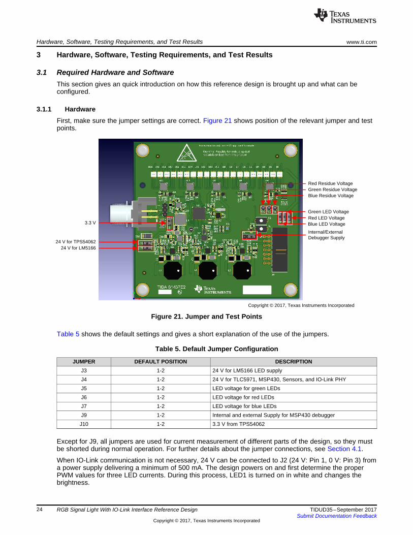
3.1.1 HardwareFirst, make sure the jumper settings are correct. Figure 21 shows position of the relevant jumper and testpoints.
Figure 21. Jumper and Test Points
Table 5 shows the default settings and gives a short explanation of the use of the jumpers.
Table 5. Default Jumper Configuration
JUMPER DEFAULT POSITION DESCRIPTIONJ3 1-2 24 V for LM5166 LED supplyJ4 1-2 24 V for TLC5971, MSP430, Sensors, and IO-Link PHYJ5 1-2 LED voltage for green LEDsJ6 1-2 LED voltage for red LEDsJ7 1-2 LED voltage for blue LEDsJ9 1-2 Internal and external Supply for MSP430 debuggerJ10 1-2 3.3 V from TPS54062
Except for J9, all jumpers are used for current measurement of different parts of the design, so they mustbe shorted during normal operation. For further details about the jumper connections, see Section 4.1.
When IO-Link communication is not necessary, 24 V can be connected to J2 (24 V: Pin 1, 0 V: Pin 3) froma power supply delivering a minimum of 500 mA. The design powers on and first determine the properPWM values for three LED currents. During this process, LED1 is turned on in white and changes thebrightness.
www.ti.com Hardware, Software, Testing Requirements, and Test Results
25TIDUD35–September 2017Submit Documentation Feedback
Copyright © 2017, Texas Instruments Incorporated
RGB Signal Light With IO-Link Interface Reference Design
Afterwards it will enter demo mode, the different implemented pattern will loop through. During this,brightness control is active. When the OPT3001 (U7) is covered, the LED brightness fades down; when itis exposed to light, the LED brightness increases.
Dynamic headroom control is also active. The voltage drop over the TLC5971 is regulated depending onthe brightness of the LEDs. So the output voltage of the three LM5166 will be different, whereas thevoltage on TP1 to TP3 will be the same.
To test the IO-Link communication, connect an IO-Link master to the connector J1. The master must becapable to deliver 24 V at 500 mA.
3.1.2 SoftwareTo get started controlling the reference design using software, a PC running Windows® and an IO-Linkmaster is required. In this example, a TMG-USB IO-Link Master V2 with the corresponding IO-Link tool isused. Connect the IO-Link master to J1 of the system.
After connecting the reference design to a powered IO-Link master, it turns on in demo mode. The IO-Linkcommunication is initialized and can be used for connecting and controlling the system. Table 3 lists theimplemented parameters.
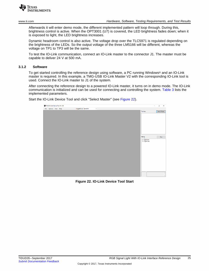
Start the IO-Link Device Tool and click "Select Master" (see Figure 22).
Figure 22. IO-Link Device Tool Start
Hardware, Software, Testing Requirements, and Test Results www.ti.com
26 TIDUD35–September 2017Submit Documentation Feedback
Copyright © 2017, Texas Instruments Incorporated
RGB Signal Light With IO-Link Interface Reference Design
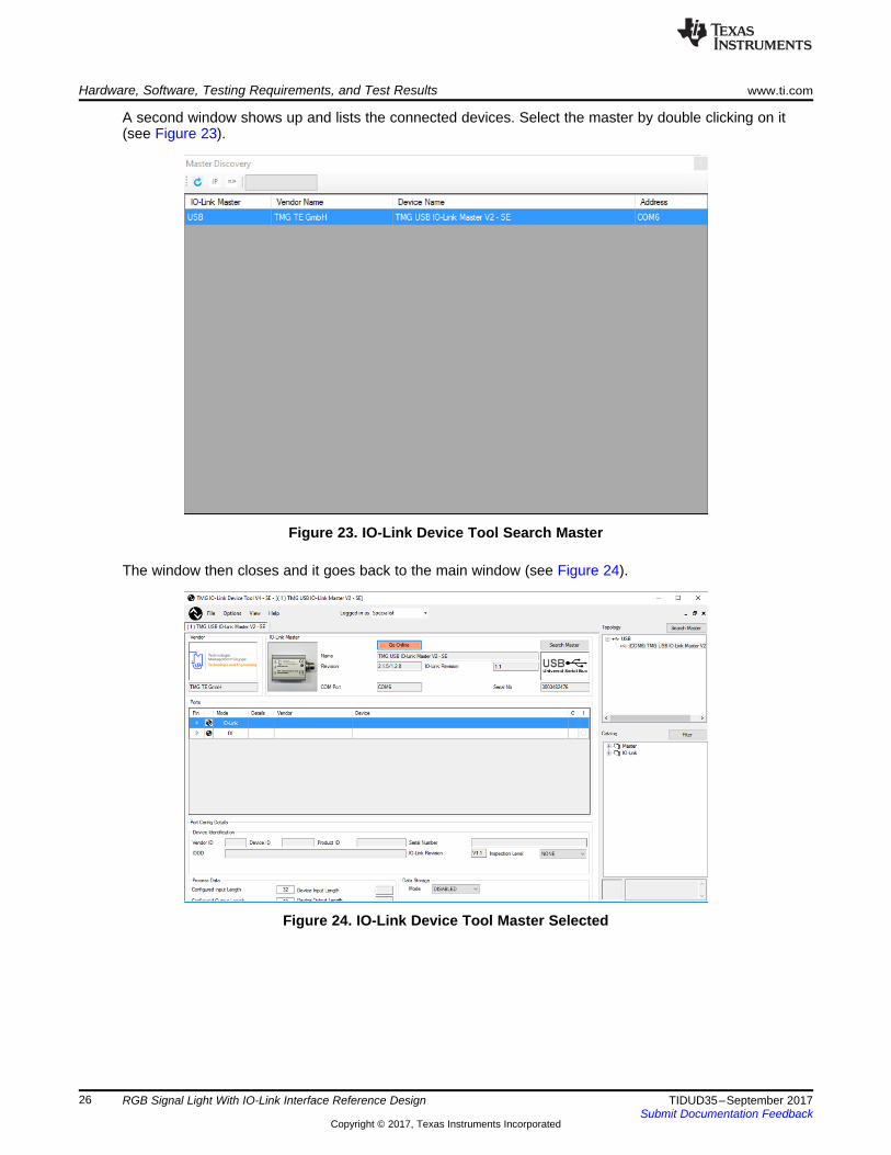
A second window shows up and lists the connected devices. Select the master by double clicking on it(see Figure 23).
Figure 23. IO-Link Device Tool Search Master
The window then closes and it goes back to the main window (see Figure 24).
Figure 24. IO-Link Device Tool Master Selected
www.ti.com Hardware, Software, Testing Requirements, and Test Results
27TIDUD35–September 2017Submit Documentation Feedback
Copyright © 2017, Texas Instruments Incorporated
RGB Signal Light With IO-Link Interface Reference Design
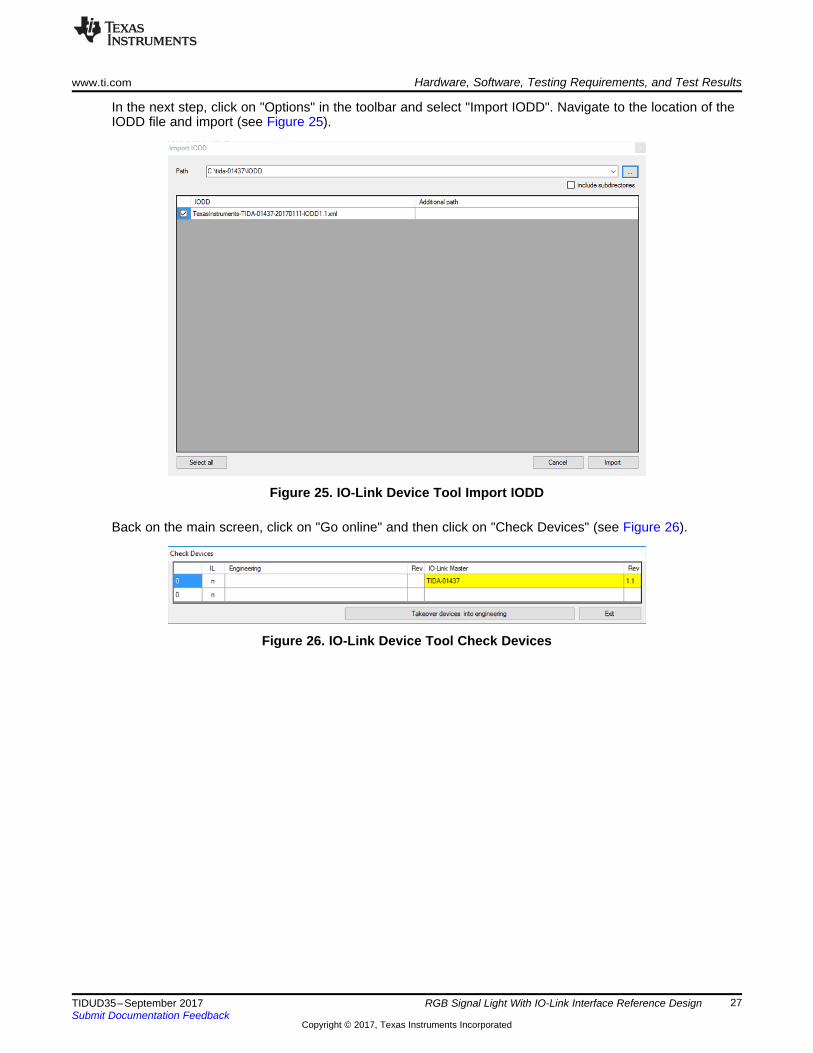
In the next step, click on "Options" in the toolbar and select "Import IODD". Navigate to the location of theIODD file and import (see Figure 25).
Figure 25. IO-Link Device Tool Import IODD
Back on the main screen, click on "Go online" and then click on "Check Devices" (see Figure 26).
Figure 26. IO-Link Device Tool Check Devices
Hardware, Software, Testing Requirements, and Test Results www.ti.com
28 TIDUD35–September 2017Submit Documentation Feedback
Copyright © 2017, Texas Instruments Incorporated
RGB Signal Light With IO-Link Interface Reference Design
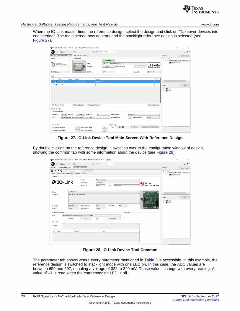
When the IO-Link master finds the reference design, select the design and click on "Takeover devices intoengineering". The main screen now appears and the stacklight reference design is selected (seeFigure 27).
Figure 27. IO-Link Device Tool Main Screen With Reference Design
By double clicking on the reference design, it switches over to the configuration window of design,showing the common tab with some information about the device (see Figure 28).
Figure 28. IO-Link Device Tool Common
The parameter tab shows where every parameter mentioned in Table 3 is accessible. In this example, thereference design is switched to stacklight mode with one LED on. In this case, the ADC values arebetween 659 and 697, equaling a voltage of 322 to 340 mV. These values change with every reading. Avalue of –1 is read when the corresponding LED is off.
www.ti.com Hardware, Software, Testing Requirements, and Test Results
29TIDUD35–September 2017Submit Documentation Feedback
Copyright © 2017, Texas Instruments Incorporated
RGB Signal Light With IO-Link Interface Reference Design
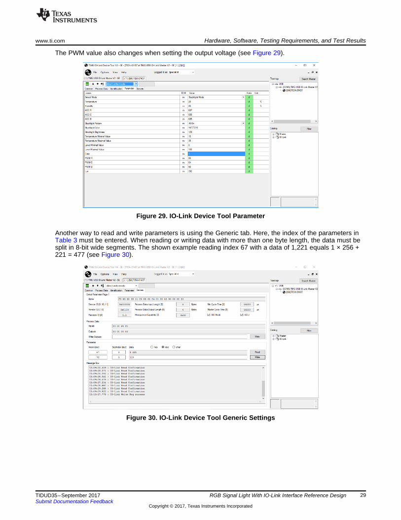
The PWM value also changes when setting the output voltage (see Figure 29).
Figure 29. IO-Link Device Tool Parameter
Another way to read and write parameters is using the Generic tab. Here, the index of the parameters inTable 3 must be entered. When reading or writing data with more than one byte length, the data must besplit in 8-bit wide segments. The shown example reading index 67 with a data of 1,221 equals 1 × 256 +221 = 477 (see Figure 30).
Figure 30. IO-Link Device Tool Generic Settings
Hardware, Software, Testing Requirements, and Test Results www.ti.com
30 TIDUD35–September 2017Submit Documentation Feedback
Copyright © 2017, Texas Instruments Incorporated
RGB Signal Light With IO-Link Interface Reference Design
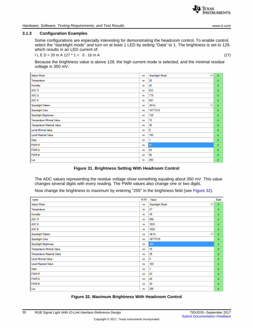
3.1.3 Configuration ExamplesSome configurations are especially interesting for demonstrating the headroom control. To enable control,select the "stacklight mode" and turn on at least 1 LED by setting "Data" to 1. The brightness is set to 129,which results in an LED current of:I L E D = 20 m A 127 * 1 = 0 . 16 m A (17)
Because the brightness value is above 128, the high current mode is selected, and the minimal residuevoltage is 350 mV.
Figure 31. Brightness Setting With Headroom Control
The ADC values representing the residue voltage show something equaling about 350 mV. This valuechanges several digits with every reading. The PWM values also change one or two digits.
Now change the brightness to maximum by entering "255" in the brightness field (see Figure 32).
Figure 32. Maximum Brightness With Headroom Control
www.ti.com Hardware, Software, Testing Requirements, and Test Results
31TIDUD35–September 2017Submit Documentation Feedback
Copyright © 2017, Texas Instruments Incorporated
RGB Signal Light With IO-Link Interface Reference Design
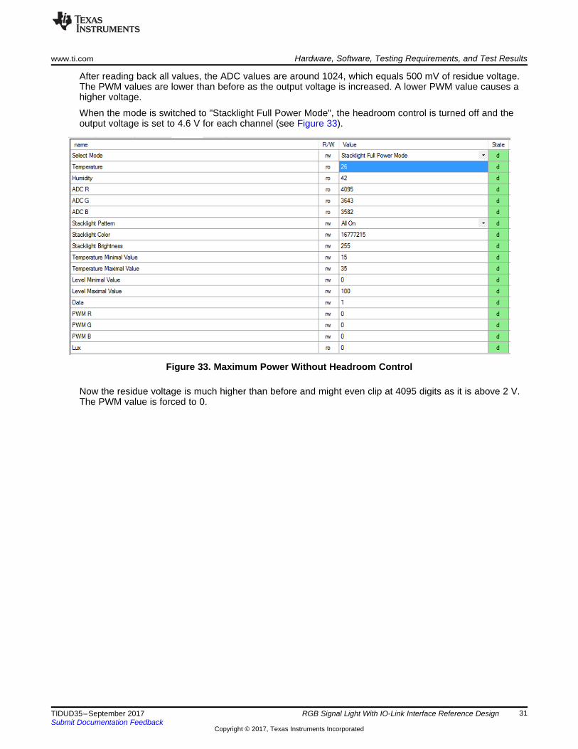
After reading back all values, the ADC values are around 1024, which equals 500 mV of residue voltage.The PWM values are lower than before as the output voltage is increased. A lower PWM value causes ahigher voltage.
When the mode is switched to "Stacklight Full Power Mode", the headroom control is turned off and theoutput voltage is set to 4.6 V for each channel (see Figure 33).
Figure 33. Maximum Power Without Headroom Control
Now the residue voltage is much higher than before and might even clip at 4095 digits as it is above 2 V.The PWM value is forced to 0.
Forward Voltage (V)
Cur
rent
(m
A)
1.5 1.7 1.9 2.1 2.3 2.5 2.7 2.90.000
0.005
0.010
0.015
0.020
0.025
D005
Red (mA)Green (mA)Blue (mA)
Hardware, Software, Testing Requirements, and Test Results www.ti.com
32 TIDUD35–September 2017Submit Documentation Feedback
Copyright © 2017, Texas Instruments Incorporated
RGB Signal Light With IO-Link Interface Reference Design
3.2 Testing and ResultsFor obtaining the measurements, a power supply is connected to the IO-Link connector. The input voltageand current is measured on J3. The output voltage and LED currents are measured on J5 to J7. Thevoltage drop on the TLC5971 on TP1 to TP3.
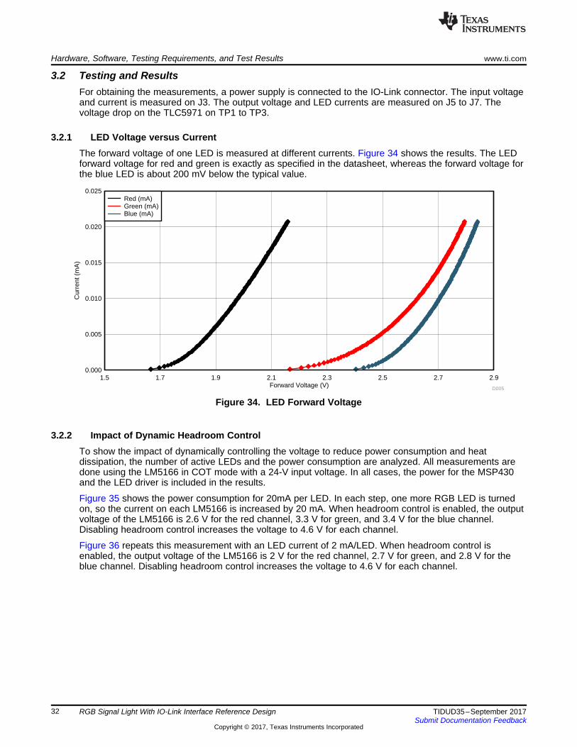
3.2.1 LED Voltage versus CurrentThe forward voltage of one LED is measured at different currents. Figure 34 shows the results. The LEDforward voltage for red and green is exactly as specified in the datasheet, whereas the forward voltage forthe blue LED is about 200 mV below the typical value.
Figure 34. LED Forward Voltage
3.2.2 Impact of Dynamic Headroom ControlTo show the impact of dynamically controlling the voltage to reduce power consumption and heatdissipation, the number of active LEDs and the power consumption are analyzed. All measurements aredone using the LM5166 in COT mode with a 24-V input voltage. In all cases, the power for the MSP430and the LED driver is included in the results.
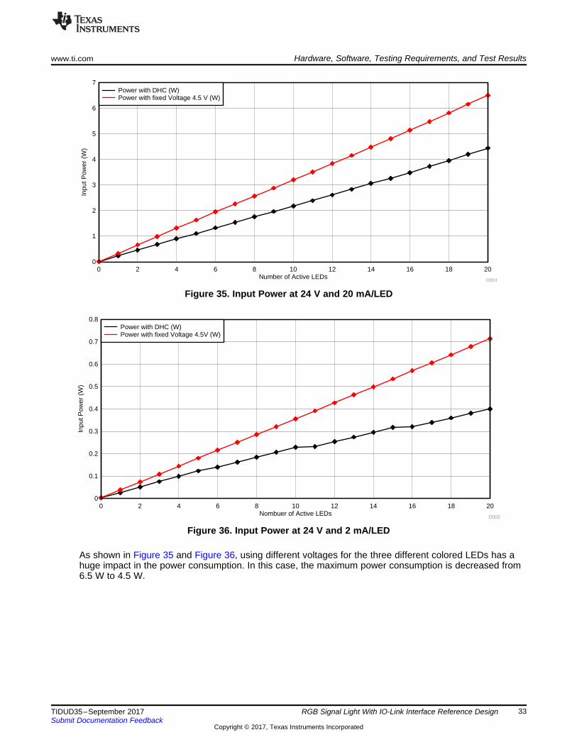
Figure 35 shows the power consumption for 20mA per LED. In each step, one more RGB LED is turnedon, so the current on each LM5166 is increased by 20 mA. When headroom control is enabled, the outputvoltage of the LM5166 is 2.6 V for the red channel, 3.3 V for green, and 3.4 V for the blue channel.Disabling headroom control increases the voltage to 4.6 V for each channel.
Figure 36 repeats this measurement with an LED current of 2 mA/LED. When headroom control isenabled, the output voltage of the LM5166 is 2 V for the red channel, 2.7 V for green, and 2.8 V for theblue channel. Disabling headroom control increases the voltage to 4.6 V for each channel.
Nombuer of Active LEDs
Inpu
t Pow
er (
W)
0 2 4 6 8 10 12 14 16 18 200
0.1
0.2
0.3
0.4
0.5
0.6
0.7
0.8
D002
Power with DHC (W)Power with fixed Voltage 4.5V (W)
Number of Active LEDs
Inpu
t Pow
er (
W)
0 2 4 6 8 10 12 14 16 18 200
1
2
3
4
5
6
7
D001
Power with DHC (W)Power with fixed Voltage 4.5 V (W)
www.ti.com Hardware, Software, Testing Requirements, and Test Results
33TIDUD35–September 2017Submit Documentation Feedback
Copyright © 2017, Texas Instruments Incorporated
RGB Signal Light With IO-Link Interface Reference Design
Figure 35. Input Power at 24 V and 20 mA/LED
Figure 36. Input Power at 24 V and 2 mA/LED
As shown in Figure 35 and Figure 36, using different voltages for the three different colored LEDs has ahuge impact in the power consumption. In this case, the maximum power consumption is decreased from6.5 W to 4.5 W.
LED Current (mA)
Vol
tage
Dro
p (V
)
0.000 0.005 0.010 0.015 0.0200.0
0.1
0.2
0.3
0.4
0.5
0.6
D007
Drop Blue (V)Drop Green (V)Drop Red (V)
LED Current (mA)
Vol
tage
Dro
p (V
)
0.000 0.005 0.010 0.015 0.0201.5
1.7
1.9
2.1
2.3
2.5
2.7
2.9
3.1
D006
Drop Blue (V)Drop Green (V)Drop Red (V)
Hardware, Software, Testing Requirements, and Test Results www.ti.com
34 TIDUD35–September 2017Submit Documentation Feedback
Copyright © 2017, Texas Instruments Incorporated
RGB Signal Light With IO-Link Interface Reference Design
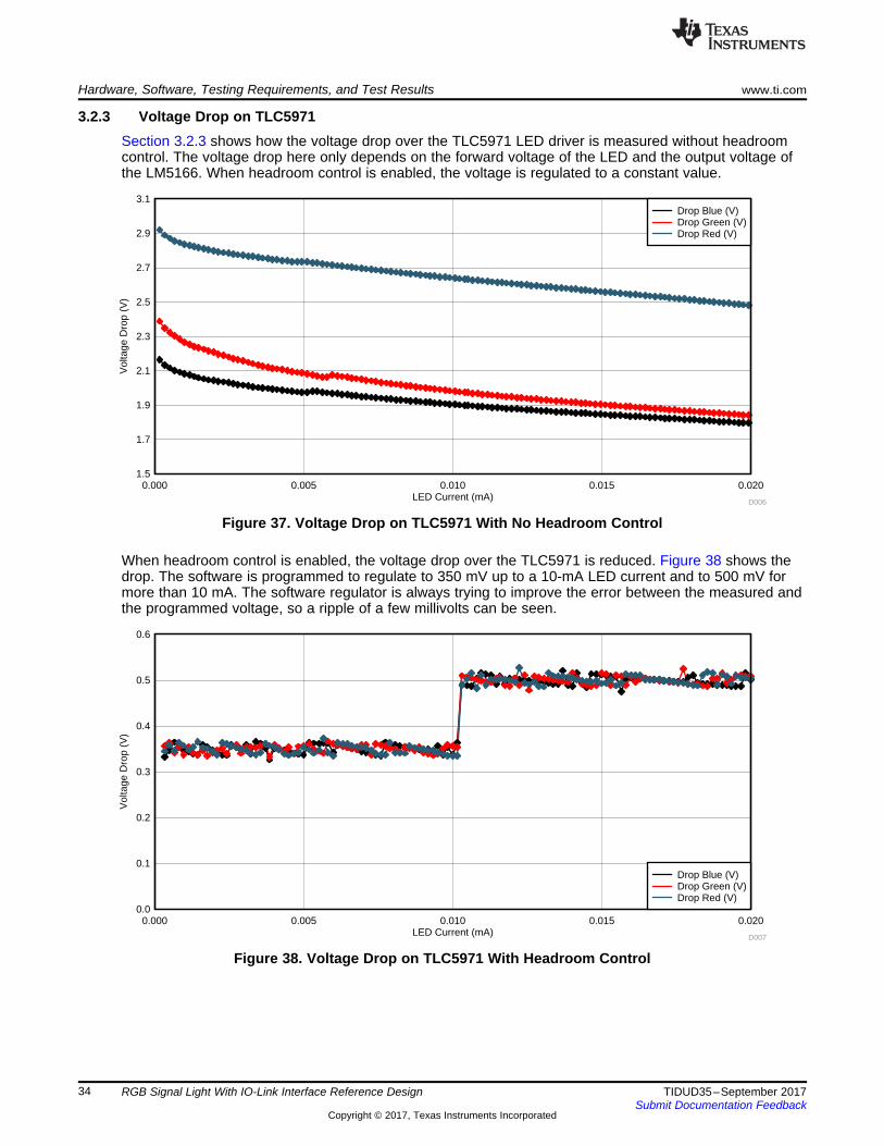
3.2.3 Voltage Drop on TLC5971Section 3.2.3 shows how the voltage drop over the TLC5971 LED driver is measured without headroomcontrol. The voltage drop here only depends on the forward voltage of the LED and the output voltage ofthe LM5166. When headroom control is enabled, the voltage is regulated to a constant value.
Figure 37. Voltage Drop on TLC5971 With No Headroom Control
When headroom control is enabled, the voltage drop over the TLC5971 is reduced. Figure 38 shows thedrop. The software is programmed to regulate to 350 mV up to a 10-mA LED current and to 500 mV formore than 10 mA. The software regulator is always trying to improve the error between the measured andthe programmed voltage, so a ripple of a few millivolts can be seen.
Figure 38. Voltage Drop on TLC5971 With Headroom Control
Output Current (mA)
Effi
cien
cy
0 50 100 150 200 250 300 350 40075%
77%
79%
81%
83%
85%
87%
89%
91%
93%
95%
D003
21 VIN (�)24 VIN (�)33 VIN (�)
Brightness Control
LED
Cur
rent
(m
A)
0 20 40 60 80 100 1200.000
0.005
0.010
0.015
0.020
0.025
D008
www.ti.com Hardware, Software, Testing Requirements, and Test Results
35TIDUD35–September 2017Submit Documentation Feedback
Copyright © 2017, Texas Instruments Incorporated
RGB Signal Light With IO-Link Interface Reference Design
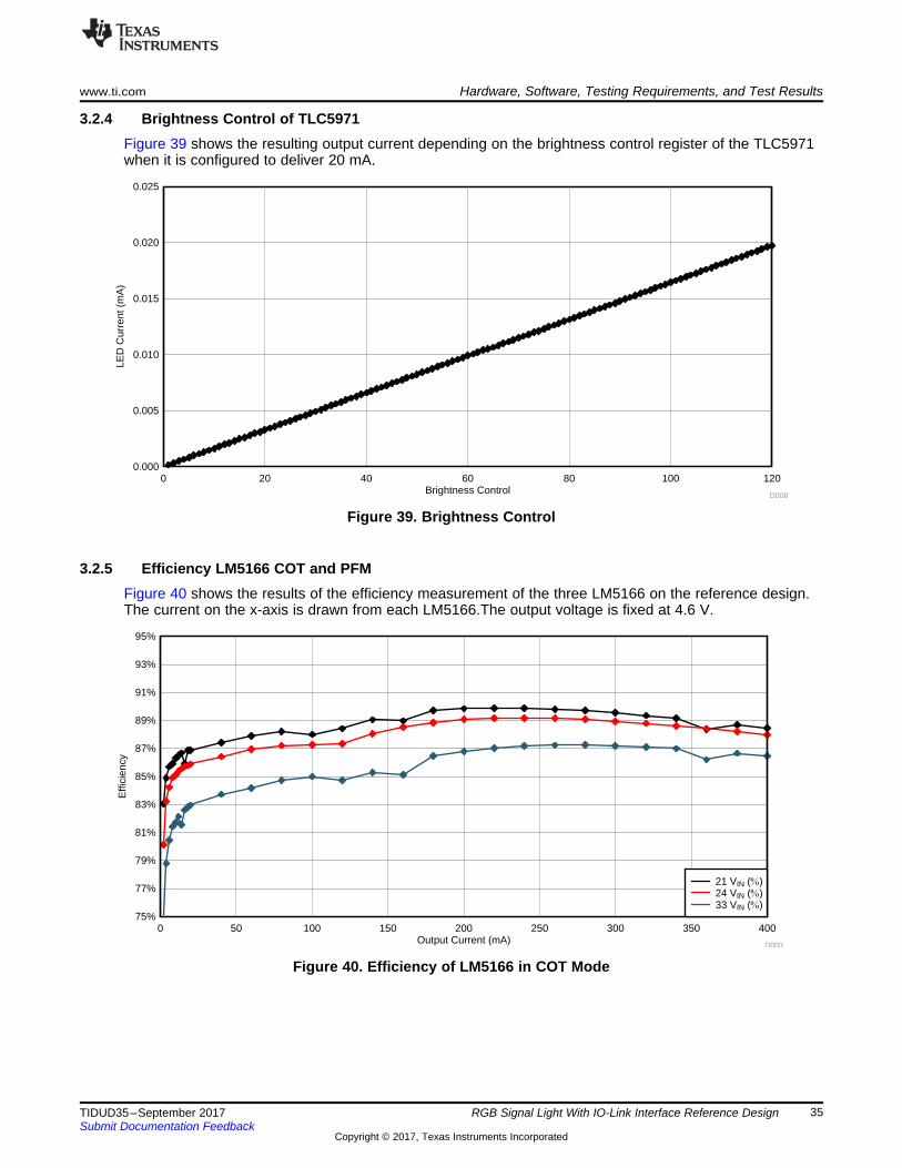
3.2.4 Brightness Control of TLC5971Figure 39 shows the resulting output current depending on the brightness control register of the TLC5971when it is configured to deliver 20 mA.
Figure 39. Brightness Control
3.2.5 Efficiency LM5166 COT and PFMFigure 40 shows the results of the efficiency measurement of the three LM5166 on the reference design.The current on the x-axis is drawn from each LM5166.The output voltage is fixed at 4.6 V.
Figure 40. Efficiency of LM5166 in COT Mode
I (mA)
Effi
cien
cy
0 50 100 150 200 250 300 350 40075%
77%
79%
81%
83%
85%
87%
89%
91%
93%
95%
D004
21 VIN (�)24 VIN (�)33 VIN (�)
Hardware, Software, Testing Requirements, and Test Results www.ti.com
36 TIDUD35–September 2017Submit Documentation Feedback
Copyright © 2017, Texas Instruments Incorporated
RGB Signal Light With IO-Link Interface Reference Design
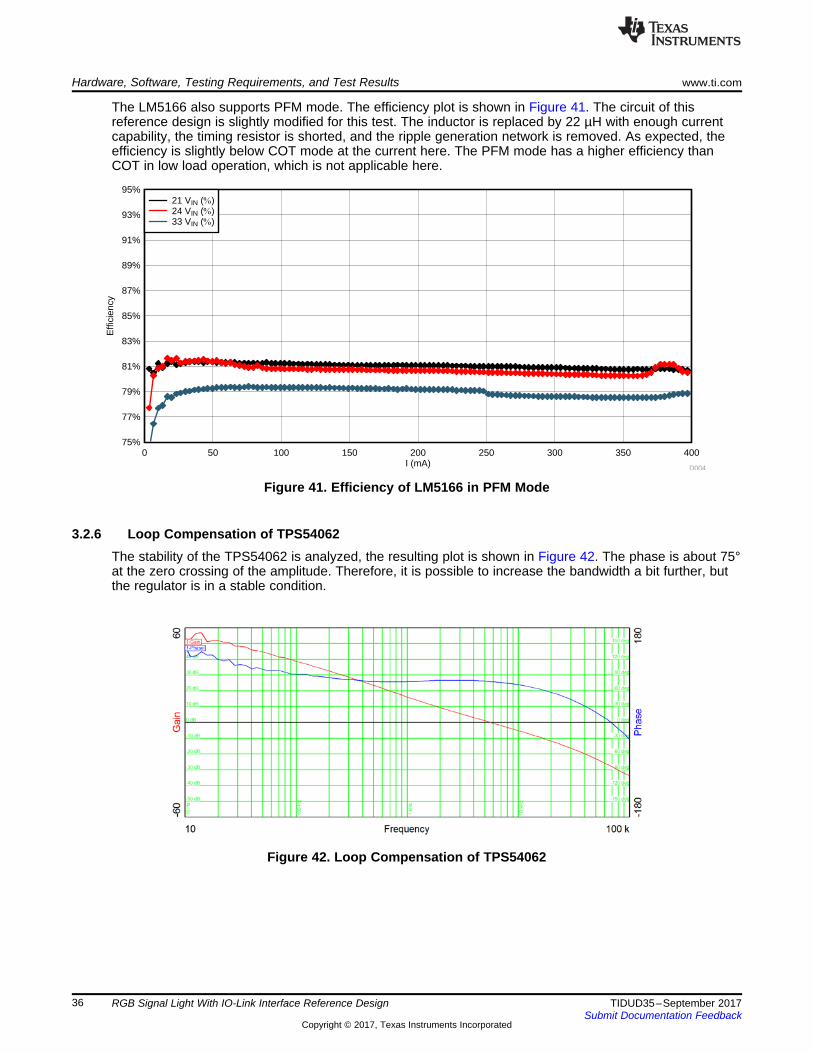
The LM5166 also supports PFM mode. The efficiency plot is shown in Figure 41. The circuit of thisreference design is slightly modified for this test. The inductor is replaced by 22 µH with enough currentcapability, the timing resistor is shorted, and the ripple generation network is removed. As expected, theefficiency is slightly below COT mode at the current here. The PFM mode has a higher efficiency thanCOT in low load operation, which is not applicable here.
Figure 41. Efficiency of LM5166 in PFM Mode
3.2.6 Loop Compensation of TPS54062The stability of the TPS54062 is analyzed, the resulting plot is shown in Figure 42. The phase is about 75°at the zero crossing of the amplitude. Therefore, it is possible to increase the bandwidth a bit further, butthe regulator is in a stable condition.
Figure 42. Loop Compensation of TPS54062
www.ti.com Design Files
37TIDUD35–September 2017Submit Documentation Feedback
Copyright © 2017, Texas Instruments Incorporated
RGB Signal Light With IO-Link Interface Reference Design
4 Design Files
4.1 SchematicsTo download the schematics, see the design files at TIDA-01437.
4.2 Bill of MaterialsTo download the bill of materials (BOM), see the design files at TIDA-01437.
4.3 PCB Layout Recommendations
4.3.1 Layout PrintsTo download the layer plots, see the design files at TIDA-01437.
4.4 Altium ProjectTo download the Altium project files, see the design files at TIDA-01437.
4.5 Gerber FilesTo download the Gerber files, see the design files at TIDA-01437.
4.6 Assembly DrawingsTo download the assembly drawings, see the design files at TIDA-01437.
5 Related Documentation
1. Cree, Inc. Cree PLCC6 3 in 1 SMD LED, Datasheet (CLY6D-FKC)
5.1 TrademarksMSP430 is a trademark of Texas Instruments.Windows is a registered trademark of Microsoft Corporation.All other trademarks are the property of their respective owners.
6 About the AuthorSTEFFEN GRAF is a systems engineer at Texas Instruments, where he is responsible for developingreference design solutions for the industrial segment. He earned his master of science in electricalengineering at the University of applied science in Darmstadt, Germany.

IMPORTANT NOTICE FOR TI DESIGN INFORMATION AND RESOURCES
Texas Instruments Incorporated (‘TI”) technical, application or other design advice, services or information, including, but not limited to,reference designs and materials relating to evaluation modules, (collectively, “TI Resources”) are intended to assist designers who aredeveloping applications that incorporate TI products; by downloading, accessing or using any particular TI Resource in any way, you(individually or, if you are acting on behalf of a company, your company) agree to use it solely for this purpose and subject to the terms ofthis Notice.TI’s provision of TI Resources does not expand or otherwise alter TI’s applicable published warranties or warranty disclaimers for TIproducts, and no additional obligations or liabilities arise from TI providing such TI Resources. TI reserves the right to make corrections,enhancements, improvements and other changes to its TI Resources.You understand and agree that you remain responsible for using your independent analysis, evaluation and judgment in designing yourapplications and that you have full and exclusive responsibility to assure the safety of your applications and compliance of your applications(and of all TI products used in or for your applications) with all applicable regulations, laws and other applicable requirements. Yourepresent that, with respect to your applications, you have all the necessary expertise to create and implement safeguards that (1)anticipate dangerous consequences of failures, (2) monitor failures and their consequences, and (3) lessen the likelihood of failures thatmight cause harm and take appropriate actions. You agree that prior to using or distributing any applications that include TI products, youwill thoroughly test such applications and the functionality of such TI products as used in such applications. TI has not conducted anytesting other than that specifically described in the published documentation for a particular TI Resource.You are authorized to use, copy and modify any individual TI Resource only in connection with the development of applications that includethe TI product(s) identified in such TI Resource. NO OTHER LICENSE, EXPRESS OR IMPLIED, BY ESTOPPEL OR OTHERWISE TOANY OTHER TI INTELLECTUAL PROPERTY RIGHT, AND NO LICENSE TO ANY TECHNOLOGY OR INTELLECTUAL PROPERTYRIGHT OF TI OR ANY THIRD PARTY IS GRANTED HEREIN, including but not limited to any patent right, copyright, mask work right, orother intellectual property right relating to any combination, machine, or process in which TI products or services are used. Informationregarding or referencing third-party products or services does not constitute a license to use such products or services, or a warranty orendorsement thereof. Use of TI Resources may require a license from a third party under the patents or other intellectual property of thethird party, or a license from TI under the patents or other intellectual property of TI.TI RESOURCES ARE PROVIDED “AS IS” AND WITH ALL FAULTS. TI DISCLAIMS ALL OTHER WARRANTIES ORREPRESENTATIONS, EXPRESS OR IMPLIED, REGARDING TI RESOURCES OR USE THEREOF, INCLUDING BUT NOT LIMITED TOACCURACY OR COMPLETENESS, TITLE, ANY EPIDEMIC FAILURE WARRANTY AND ANY IMPLIED WARRANTIES OFMERCHANTABILITY, FITNESS FOR A PARTICULAR PURPOSE, AND NON-INFRINGEMENT OF ANY THIRD PARTY INTELLECTUALPROPERTY RIGHTS.TI SHALL NOT BE LIABLE FOR AND SHALL NOT DEFEND OR INDEMNIFY YOU AGAINST ANY CLAIM, INCLUDING BUT NOTLIMITED TO ANY INFRINGEMENT CLAIM THAT RELATES TO OR IS BASED ON ANY COMBINATION OF PRODUCTS EVEN IFDESCRIBED IN TI RESOURCES OR OTHERWISE. IN NO EVENT SHALL TI BE LIABLE FOR ANY ACTUAL, DIRECT, SPECIAL,COLLATERAL, INDIRECT, PUNITIVE, INCIDENTAL, CONSEQUENTIAL OR EXEMPLARY DAMAGES IN CONNECTION WITH ORARISING OUT OF TI RESOURCES OR USE THEREOF, AND REGARDLESS OF WHETHER TI HAS BEEN ADVISED OF THEPOSSIBILITY OF SUCH DAMAGES.You agree to fully indemnify TI and its representatives against any damages, costs, losses, and/or liabilities arising out of your non-compliance with the terms and provisions of this Notice.This Notice applies to TI Resources. Additional terms apply to the use and purchase of certain types of materials, TI products and services.These include; without limitation, TI’s standard terms for semiconductor products http://www.ti.com/sc/docs/stdterms.htm), evaluationmodules, and samples (http://www.ti.com/sc/docs/sampterms.htm).
Mailing Address: Texas Instruments, Post Office Box 655303, Dallas, Texas 75265Copyright © 2017, Texas Instruments Incorporated