Embed Size (px)
Citation preview
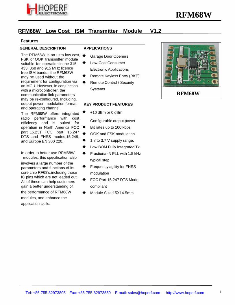
RFM68W
Tel: +86-755-82973805 Fax: +86-755-82973550 E-mail: [email protected] http://www.hoperf.com
1
RFM68W Low Cost ISM Transmitter Module V1.2
Features
GENERAL DESCRIPTION
The RFM68W is an ultra-low-cost, FSK or OOK transmitter module suitable for operation in the 315, 433, 868 and 915 MHz licence free ISM bands., the RFM68W may be used without the requirement for configuration via an MCU. However, in conjunction with a microcontroller, the communication link parameters may be re-configured. Including, output power, modulation format and operating channel. The RFM68W offers integrated radio performance with cost efficiency and is suited for operation in North America FCC part 15.231, FCC part 15.247 DTS and FHSS modes,15.249, and Europe EN 300 220. In order to better use RFM68W modules, this specification also involves a large number of the parameters and functions of its core chip RF68's,including those IC pins which are not leaded out. All of these can help customers gain a better understanding of the performance of RFM68W modules, and enhance the application skills.
APPLICATIONS
Garage Door Openers
Low-Cost Consumer
Electronic Applications
Remote Keyless Entry (RKE)
Remote Control / Security
Systems KEY PRODUCT FEATURES
+10 dBm or 0 dBm
Configurable output power
Bit rates up to 100 kbps
OOK and FSK modulation.
1.8 to 3.7 V supply range.
Low BOM Fully Integrated Tx
Fractional-N PLL with 1.5 kHz
typical step
Frequency agility for FHSS
modulation
FCC Part 15.247 DTS Mode
compliant
Module Size:15X14.5mm
RFM68W
RFM68W
2
Tel: +86-755-82973805 Fax: +86-755-82973550 E-mail: [email protected] http:/ /www.hoperf.com
Table of contents
Section Page
1. Circuit Description.................................................................................................................................................... 3 1.1. General Description ......................................................................................................................................... 3 1.2. Block Diagram.................................................................................................................................................. 3 1.3. Pin Description,............................................................................................................................................ 4
2. Electrical Characteristics ......................................................................................................................................... 5 2.1. ESD Notice ...................................................................................................................................................... 5 2.2. Absolute Maximum Ratings ............................................................................................................................. 5 2.3. Operating Range.............................................................................................................................................. 5 2.4. Electrical Specifications....................................................................................................................................... 6
3. Timing Characteristics ............................................................................................................................................. 7 4. Application Modes of the RFM68W............................................................................................................................8
4.1. Transmitter Modes ........................................................................................................................................... 8 4.2. Mode Selection Flowchart................................................................................................................................ 9 4.3. Application Mode: Power & Go ....................................................................................................................... 10 4.4. Application Mode: Advanced ......................................................................................................................... 10
4.4.1. Advanced Mode: Configuration............................................................................................................... 10 4.4.2. Frequency Hopping Spread Spectrum.................................................................................................... 10
4.5. Frequency Band Coverage ............................................................................................................................ 11 4.6. Power Consumption.........................................................................................................................................11
5. RFM68W Configuration............................................................................................................................................12 5.1. TWI Access ......................................................................................................................................................12 5.2. APPLICATION Configuration Parameters ..................................................................................................... 14 5.3. FREQUENCY Configuration Parameters ...................................................................................................... 14 5.4. Test Parameters (internal) ............................................................................................................................. 15 5.5. Status Parameters ......................................................................................................................................... 15 5.6. Recovery Command ....................................................................................................................................... 16
6. Application Information .......................................................................................................................................... 17 6.1. Reference Design .......................................................................................................................................... 17 6.2. NRESET Pin ................................................................................................................................................... 18 6.3. TX_READY Pin ............................................................................................................................................... 18 6.4. Low Power Optimization ................................................................................................................................. 18
6.4.1. 2 Connections: CTRL, DATA ................................................................................................................... 18 6.4.2. 3 Connections: CTRL, DATA, TX_READY .............................................................................................. 18
7. RFM68W Packaging .................................................................................................................................................19 7.1. S2 Package Outline Drawing ...........................................................................................................................19
8. Ordering Information………………………………………………………………………………………………………….20
RFM68W RFM68W
3
Tel: +86-755-82973805 Fax: +86-755-82973550 E-mail: [email protected] http:/ /www.hoperf.com
This product datasheet contains a detailed description of the RFM68W performance and functionality.
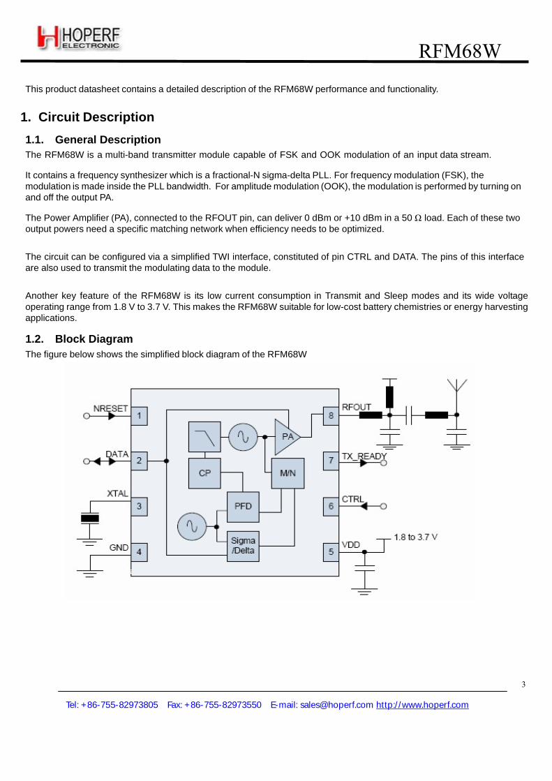
1. Circuit Description 1.1. General Description The RFM68W is a multi-band transmitter module capable of FSK and OOK modulation of an input data stream.
It contains a frequency synthesizer which is a fractional-N sigma-delta PLL. For frequency modulation (FSK), the modulation is made inside the PLL bandwidth. For amplitude modulation (OOK), the modulation is performed by turning on and off the output PA.
The Power Amplifier (PA), connected to the RFOUT pin, can deliver 0 dBm or +10 dBm in a 50 Ω load. Each of these two output powers need a specific matching network when efficiency needs to be optimized.
The circuit can be configured via a simplified TWI interface, constituted of pin CTRL and DATA. The pins of this interface are also used to transmit the modulating data to the module.
Another key feature of the RFM68W is its low current consumption in Transmit and Sleep modes and its wide voltage operating range from 1.8 V to 3.7 V. This makes the RFM68W suitable for low-cost battery chemistries or energy harvesting applications.
1.2. Block Diagram The figure below shows the simplified block diagram of the RFM68W
RFM68W RFM68W
4
Tel: +86-755-82973805 Fax: +86-755-82973550 E-mail: [email protected] http:/ /www.hoperf.com
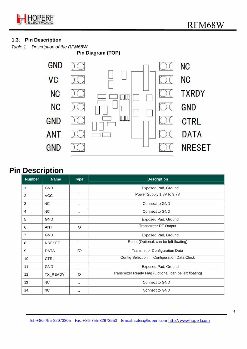
1.3. Pin Description Table 1 Description of the RFM68W
Pin Diagram (TOP)
Pin Description
Number
Name
Type
Description
1 GND I Exposed Pad, Ground 2 VCC I Power Supply 1.8V to 3.7V
3 NC - Connect to GND
4 NC - Connect to GND 5 GND I Exposed Pad, Ground 6 ANT O Transmitter RF Output
7 GND I Exposed Pad, Ground 8 NRESET I Reset (Optional, can be left floating)
9 DATA I/O Transmit or Configuration Data
10 CTRL I Config Selection Configuration Data Clock
11 GND I Exposed Pad, Ground 12 TX_READY O Transmitter Ready Flag (Optional, can be left floating)
13 NC - Connect to GND
14 NC - Connect to GND
RFM68W RFM68W
5
Tel: +86-755-82973805 Fax: +86-755-82973550 E-mail: [email protected] http:/ /www.hoperf.com
2. Electrical Characteristics
2.1. ESD Notice The RFM68W is an electrostatic discharge sensitive device. It satisfies Class 2 of the JEDEC standard JESD22-A114-B (human body model) on all pins.
2.2. Absolute Maximum Ratings Stresses above the values listed below may cause permanent device failure. Exposure to absolute maximum ratings for extended periods may affect device reliability.
Table 2 Absolute Maximum Ratings
Symbol Description Min Max Unit
VDDmr Supply Voltage -0.5 3.9 V Tmr Temperature -55 115 ° C Tjunc Junction Temperature -55 125 ° C Tstor Storage Temperature -55 150 ° C
2.3. Operating Range Operating ranges define the limits for functional operation and the parametric characteristics of the device as described in this section. Functionality outside these limits is not implied.
Table 3 Operating Range
Symbol
Description
Min
Max
Unit
VDDop Supply voltage 1.8 3.7 V Top Operational temperature range -40 85 ° C Clop Load capacitance on digital ports - 25 pF
RFM68W RFM68W
6
Tel: +86-755-82973805 Fax: +86-755-82973550 E-mail: [email protected] http:/ /www.hoperf.com
2.4. Electrical Specifications The table below gives the electrical specifications of the transmitter under the following conditions: Supply voltage = 3.3 V, temperature = 25 °C, fXOSC = 26 MHz, fRF = 915 MHz, 2-FSK modulation with Fdev=+/-10 kHz, bit rate = 10 kbit/s and output power = +10 dBm terminated in a matched 50 Ohm impedance, unless otherwise specified. Table 4 Transmitter Specifications
Symbol
Description
Conditions
Min
Typ
Max
Unit
Current Consumption IDDSL Supply current in Sleep mode - 0.5 1 µA IDDT_315 Supply current in Transmit mode
at 315 MHz* RFOP=+10dBm 50% OOK
RFOP=+10dBm FSK RFOP=0dBm FSK
- - -
11 15 9
- - -
mA mA mA
IDDT_915 Supply current in Transmit mode at 915 MHz*
RFOP=+10dBm FSK RFOP=0dBm FSK
- -
17.5 10.5
- -
mA mA
RF and Baseband Specifications Band0,For 315MHz Module 312 380 MHz Band0,For 433MHz Module 380 450 MHz Band0,For 868MHz Module 860 870 MHz
FBAND Operation Frequency Bands
Band1,For 915MHz Module 902 928 MHz FDA Frequency deviation, FSK 10 - 200 kHz BRF Bit rate, FSK Permissible Range 0.5 - 100 kbps BRO Bit rate, OOK Permissible Range 0.5 - 10 kbps OOK_B OOK Modulation Depth - 45 - dB RFOP RF output power in 50 Ohms
in either frequency band High Power SettingLow Power Setting*
7 -3
10 0
- -
dBm dBm
RFOPFL RF output power flatness From 315 to 380 MHz, 50 Ohms load - 2 - dB DRFOPV Variation in RF output power with
supply voltage 2.5 V to 3.3 V1.8 V to 3.7 V
- -
- -
3 7
dB dB
PHN Transmitter phase noise At offset: 100 kHz350 kHz550 kHz
1.15 MHz
- - - -
-82 -92 -96 -103
-76 -81 -91
-101
dBc/Hz dBc/Hz dBc/Hz dBc/Hz
STEP_22 RF frequency step FXOSC = 24 MHz,for 315MHz module - 1.46484 - kHz STEP_26 RF frequency step FXOSC = 26MHz, for 433,868MHz
module - 1.58691 - kHz
STEP_26 RF frequency step FXOSC = 26MHz, for 915MHz module 3.17383 - kHz
RFM68W RFM68W
7
Tel: +86-755-82973805 Fax: +86-755-82973550 E-mail: [email protected] http:/ /www.hoperf.com
Symbol
Description
Conditions
Min
Typ
Max
Unit
FXOSC Crystal Oscillator Frequency For 315MHz Module For 433,868,915MHz Module
24 26
MHz MHz
DFXOSC Frequency Variation of the XOSC No crystal contribution - - +/-25 ppm Timing Specifications TS_TR Time from Sleep to Tx mode XTAL dependant, with spec’d XTAL - 650 2000 us TS_HOP0 Channel hop time in Band 0 315 to 390 MHz - 250 500 us TS_HOP1 Channel hop time in Band 1 Maximum hop of 26 MHz*** - 200 400 us TOFFT Timer from Tx data activity to
Sleep Programmable -
- 2
20 - -
ms ms
RAMP PA Ramp up and down time - 20 - us T_START Time before CTRL pin mode
selection. Time from power on to sampling of CTRL **
- 200 us + TS_OSC
- ms
* With different matching networks ** The oscillator startup time, TS_OSC, depends on the electrical characteristics of the crystal *** From the last CTRL falling edge of the Frequency change instruction to transmitter ready (PA ramp up finished)
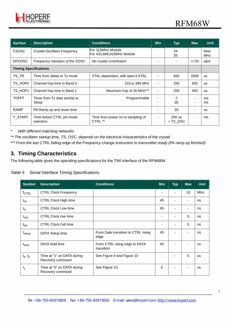
3. Timing Characteristics The following table gives the operating specifications for the TWI interface of the RFM68W.
Table 5 Serial Interface Timing Specifications
Symbol Description Conditions Min Typ Max Unit
fCTRL CTRL Clock Frequency - - 10 MHz
tch CTRL Clock High time 45 - - ns
tcl CTRL Clock Low time 45 - - ns
trise CTRL Clock rise time - - 5 ns
tfall CTRL Clock Fall time - - 5 ns
tsetup
DATA Setup time From Data transition to CTRL rising edge
45 - - ns
thold DATA hold time From CTRL rising edge to DATA transition
45 - - ns
t0, t2 Time at “1” on DATA during Recovery command
See Figure 9 and Figure 10 - - 5 us
t1 Time at “0” on DATA during Recovery command
See Figure 10 5 - - us
RFM68W RFM68W
8
Tel: +86-755-82973805 Fax: +86-755-82973550 E-mail: [email protected] http:/ /www.hoperf.com
4. Application Modes of the RFM68W Pins CTRL and DATA are used for both configuring the circuit and sending the data to be transmitted over the air. Two different modes are associated to these pins, “Power&Go” and “Advanced” modes.
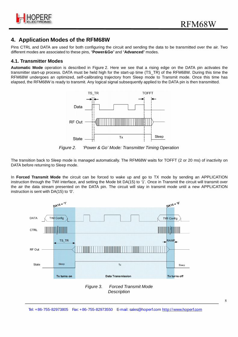
4.1. Transmitter Modes Automatic Mode operation is described in Figure 2. Here we see that a rising edge on the DATA pin activates the transmitter start-up process. DATA must be held high for the start-up time (TS_TR) of the RFM68W. During this time the RFM68W undergoes an optimized, self-calibrating trajectory from Sleep mode to Transmit mode. Once this time has elapsed, the RFM68W is ready to transmit. Any logical signal subsequently applied to the DATA pin is then transmitted.
Figure 2. ‘Power & Go’ Mode: Transmitter Timing Operation The transition back to Sleep mode is managed automatically. The RFM68W waits for TOFFT (2 or 20 ms) of inactivity on DATA before returning to Sleep mode.
In Forced Transmit Mode the circuit can be forced to wake up and go to TX mode by sending an APPLICATION instruction through the TWI interface, and setting the Mode bit DA(15) to ‘1’. Once in Transmit the circuit will transmit over the air the data stream presented on the DATA pin. The circuit will stay in transmit mode until a new APPLICATION instruction is sent with DA(15) to ‘0’.
Figure 3. Forced Transmit Mode Description
RFM68W RFM68W
9
Tel: +86-755-82973805 Fax: +86-755-82973550 E-mail: [email protected] http:/ /www.hoperf.com
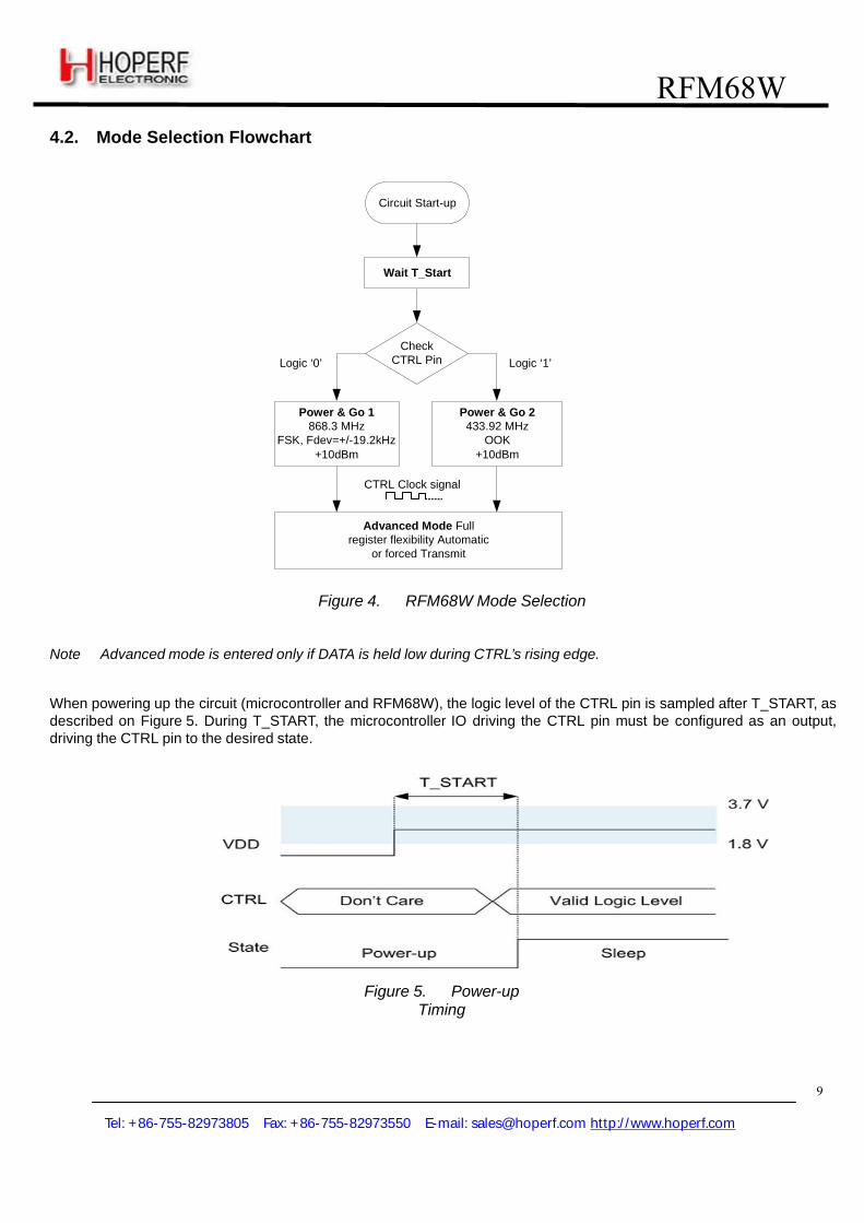
4.2. Mode Selection Flowchart
Circuit Start-up
Wait T_Start
Logic ‘0’ Check
CTRL Pin Logic ‘1’
Power & Go 1 868.3 MHz
FSK, Fdev=+/-19.2kHz +10dBm
Power & Go 2 433.92 MHz
OOK +10dBm
CTRL Clock signal
Advanced Mode Full register flexibility Automatic
or forced Transmit
Figure 4. RFM68W Mode Selection
Note Advanced mode is entered only if DATA is held low during CTRL’s rising edge.
When powering up the circuit (microcontroller and RFM68W), the logic level of the CTRL pin is sampled after T_START, as described on Figure 5. During T_START, the microcontroller IO driving the CTRL pin must be configured as an output, driving the CTRL pin to the desired state.
Figure 5. Power-up Timing
10
RFM68W RFM68W
Tel: +86-755-82973805 Fax: +86-755-82973550 E-mail: [email protected] http:/ /www.hoperf.com
4.3. Application Mode: Power &Go The default ‘Power & Go’ application mode sees the RFM68W configured as detailed in Table 6. By changing the logical state of the CTRL pin at Power-up or Reset, two distinct configuration modes can be selected. The Power & Go application modes hence permit microcontroller-less operation.
Table 6 Configuration in Power & Go Mode
CTRL Pin Configuration Mode
‘Low’ FSK 868.3 MHz, +10 dBm, Fdev=+/-19.2 kHz
Power&Go 1
‘High’ OOK 433.92 MHz, +10 dBm Power&Go 2 4.4. Application Mode: Advanced
4.4.1. Advanced Mode: Configuration As described on Figure 4, Advanced mode is entered when accessing the Two Wire Interface (TWI) bus of the RFM68W. Upon communication to the register at up to 10 MHz of clocking speed, complete flexibility on the use of the module is obtained. Once all register settings are selected (see registers detailed description in section [5]), the RFM68W can be used either in Automatic mode by simply toggling the DATA pin, or in Forced Transmit mode to optimize timings for instance.
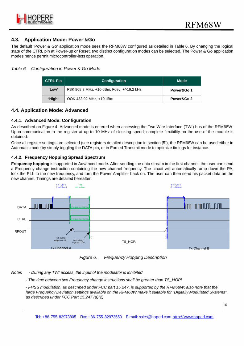
4.4.2. Frequency Hopping Spread Spectrum Frequency hopping is supported in Advanced mode. After sending the data stream in the first channel, the user can send a Frequency change instruction containing the new channel frequency. The circuit will automatically ramp down the PA, lock the PLL to the new frequency, and turn the Power Amplifier back on. The user can then send his packet data on the new channel. Timings are detailed hereafter:
t < TOFFT
(2 or 20 ms)
TWI
instruction
t < TOFFT
(2 or 20 ms)
DATA Frequency change
CTRL Frequency change
RFOUT
5th falling edge on CTRL 24th falling
edge on CTRL
Tx Channel A
TS_HOPi
Tx Channel B
Figure 6. Frequency Hopping Description
Notes - During any TWI access, the input of the modulator is inhibited
- The time between two Frequency change instructions shall be greater than TS_HOPi
- FHSS modulation, as described under FCC part 15.247, is supported by the RFM68W; also note that the large Frequency Deviation settings available on the RFM68W make it suitable for “Digitally Modulated Systems”, as described under FCC Part 15.247 (a)(2)
11
RFM68W RFM68W
Tel: +86-755-82973805 Fax: +86-755-82973550 E-mail: [email protected] http:/ /www.hoperf.com
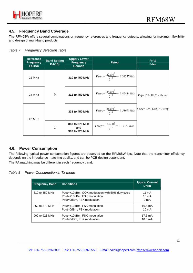
4.5. Frequency Band Coverage The RFM68W offers several combinations or frequency references and frequency outputs, allowing for maximum flexibility and design of multi-band products:
Table 7 Frequency Selection Table
Reference Frequency
FXOSC
Band Setting
DA(13) Upper / Lower
Frequency Bounds
Fstep
Frf & Fdev
22 MHz
310 to 450 MHz
22x106 Fste p= ----------------- = 1.34277kHz
214
24 MHz
312 to 450 MHz
24x106 Fste p= ----------------- = 1.46484kHz
214
0
338 to 450 MHz
26x106 Fste p= ----------------- = 1.58691kHz
214
26 MHz
1
860 to 870 MHz and
902 to 928 MHz
6
Fstep= 2---6----x---1---0---- = 3.17383kHz 213
Frf= DF( 18;0 ) × Fstep
Fde v= DA( 12;5 ) × Fstep
4.6. Power Consumption The following typical power consumption figures are observed on the RFM68W kits. Note that the transmitter efficiency depends on the impedance matching quality, and can be PCB design dependant. The PA matching may be different in each frequency band.
Table 8 Power Consumption in Tx mode
Frequency Band
Conditions
Typical Current Drain
310 to 450 MHz Pout=+10dBm, OOK modulation with 50% duty cycle Pout=+10dBm, FSK modulation Pout=0dBm, FSK modulation
11 mA 15 mA 9 mA
860 to 870 MHz Pout=+10dBm, FSK modulation Pout=0dBm, FSK modulation
16.5 mA 10 mA
902 to 928 MHz Pout=+10dBm, FSK modulation Pout=0dBm, FSK modulation
17.5 mA 10.5 mA
12
RFM68W RFM68W
Tel: +86-755-82973805 Fax: +86-755-82973550 E-mail: [email protected] http:/ /www.hoperf.com
5. RFM68W Configuration The RFM68W has several configuration parameters which can be selected through the serial interface
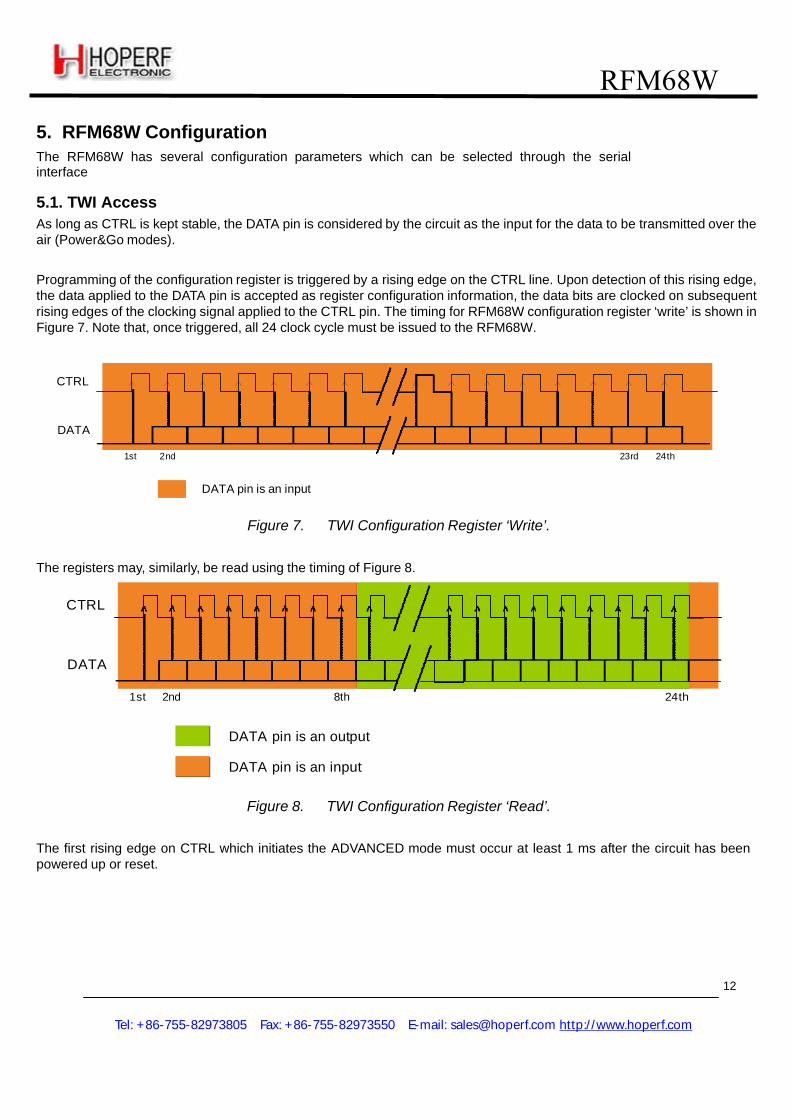
5.1. TWI Access As long as CTRL is kept stable, the DATA pin is considered by the circuit as the input for the data to be transmitted over the air (Power&Go modes).
Programming of the configuration register is triggered by a rising edge on the CTRL line. Upon detection of this rising edge, the data applied to the DATA pin is accepted as register configuration information, the data bits are clocked on subsequent rising edges of the clocking signal applied to the CTRL pin. The timing for RFM68W configuration register ‘write’ is shown in Figure 7. Note that, once triggered, all 24 clock cycle must be issued to the RFM68W.
CTRL
DATA
1st 2nd 23rd 24th
DATA pin is an input
Figure 7. TWI Configuration Register ‘Write’.
The registers may, similarly, be read using the timing of Figure 8.
CTRL
DATA
1st 2nd 8th 24th
DATA pin is an output
DATA pin is an input
Figure 8. TWI Configuration Register ‘Read’. The first rising edge on CTRL which initiates the ADVANCED mode must occur at least 1 ms after the circuit has been powered up or reset.
13
RFM68W RFM68W
Tel: +86-755-82973805 Fax: +86-755-82973550 E-mail: [email protected] http:/ /www.hoperf.com
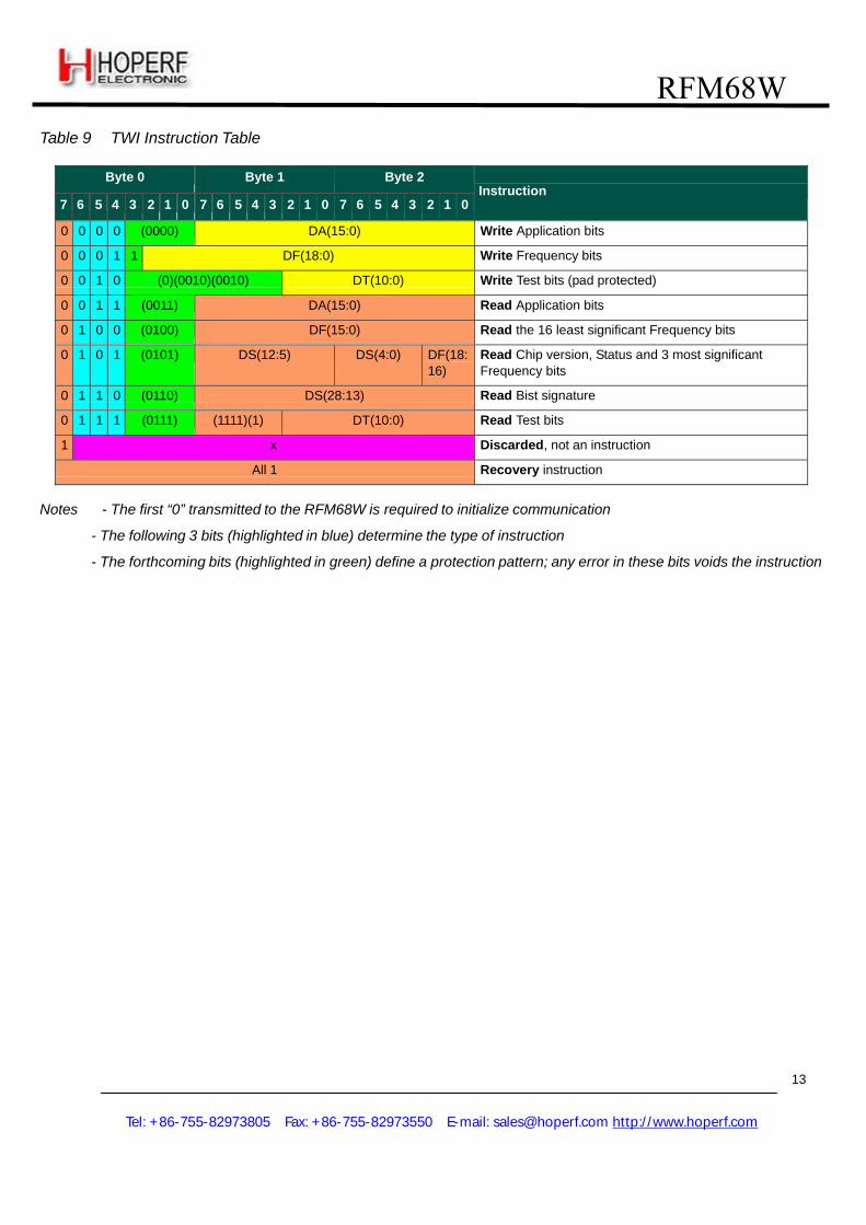
Table 9 TWI Instruction Table
Byte 0 Byte 1 Byte 2
7 6 5 4 3 2 1 0 7 6 5 4 3 2 1 0 7 6 5 4 3 2 1 0
Instruction
0 0 0 0 (0000) DA(15:0) Write Application bits 0 0 0 1 1 DF(18:0) Write Frequency bits 0 0 1 0 (0)(0010)(0010) DT(10:0) Write Test bits (pad protected) 0 0 1 1 (0011) DA(15:0) Read Application bits 0 1 0 0 (0100) DF(15:0) Read the 16 least significant Frequency bits 0 1 0 1 (0101) DS(12:5) DS(4:0) DF(18:
16) Read Chip version, Status and 3 most significant Frequency bits
0 1 1 0 (0110) DS(28:13) Read Bist signature 0 1 1 1 (0111) (1111)(1) DT(10:0) Read Test bits 1 x Discarded, not an instruction
All 1 Recovery instruction Notes - The first “0” transmitted to the RFM68W is required to initialize communication
- The following 3 bits (highlighted in blue) determine the type of instruction
- The forthcoming bits (highlighted in green) define a protection pattern; any error in these bits voids the instruction
14
RFM68W RFM68W
Tel: +86-755-82973805 Fax: +86-755-82973550 E-mail: [email protected] http:/ /www.hoperf.com
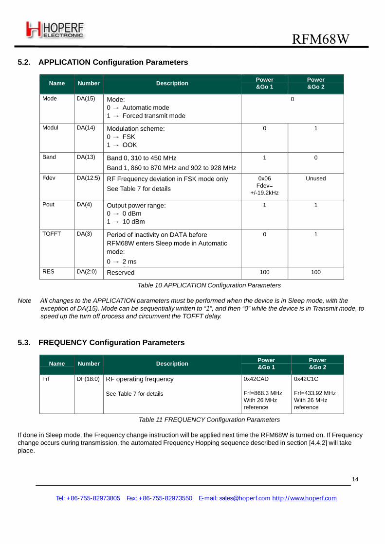
5.2. APPLICATION Configuration Parameters
Name
Number
Description Power &Go 1
Power &Go 2
Mode DA(15) Mode: 0 → Automatic mode 1 → Forced transmit mode
0
Modul DA(14) Modulation scheme: 0 → FSK 1 → OOK
0 1
Band DA(13) Band 0, 310 to 450 MHz Band 1, 860 to 870 MHz and 902 to 928 MHz
1 0
Fdev DA(12:5) RF Frequency deviation in FSK mode only See Table 7 for details
0x06 Fdev=
+/-19.2kHz
Unused
Pout DA(4) Output power range: 0 → 0 dBm 1 → 10 dBm
1 1
TOFFT DA(3) Period of inactivity on DATA before RFM68W enters Sleep mode in Automatic mode: 0 → 2 ms 1 20
0 1
RES DA(2:0) Reserved 100 100
Table 10 APPLICATION Configuration Parameters Note All changes to the APPLICATION parameters must be performed when the device is in Sleep mode, with the
exception of DA(15). Mode can be sequentially written to “1”, and then “0” while the device is in Transmit mode, to speed up the turn off process and circumvent the TOFFT delay.
5.3. FREQUENCY Configuration Parameters
Name
Number
Description Power &Go 1
Power &Go 2
Frf DF(18:0) RF operating frequency See Table 7 for details
0x42CAD Frf=868.3 MHz With 26 MHz reference
0x42C1C Frf=433.92 MHz With 26 MHz reference
Table 11 FREQUENCY Configuration Parameters If done in Sleep mode, the Frequency change instruction will be applied next time the RFM68W is turned on. If Frequency change occurs during transmission, the automated Frequency Hopping sequence described in section [4.4.2] will take place.
15
RFM68W RFM68W
Tel: +86-755-82973805 Fax: +86-755-82973550 E-mail: [email protected] http:/ /www.hoperf.com
5.4. Test Parameters (internal) Ten Test bits DT(9:0) exist in the RFM68W. They are only use for the industrial test of the device, and therefore they are pad protected. It means that their value cannot be modified without applying a specific logical level to some of the RFM68W pads during a write access.
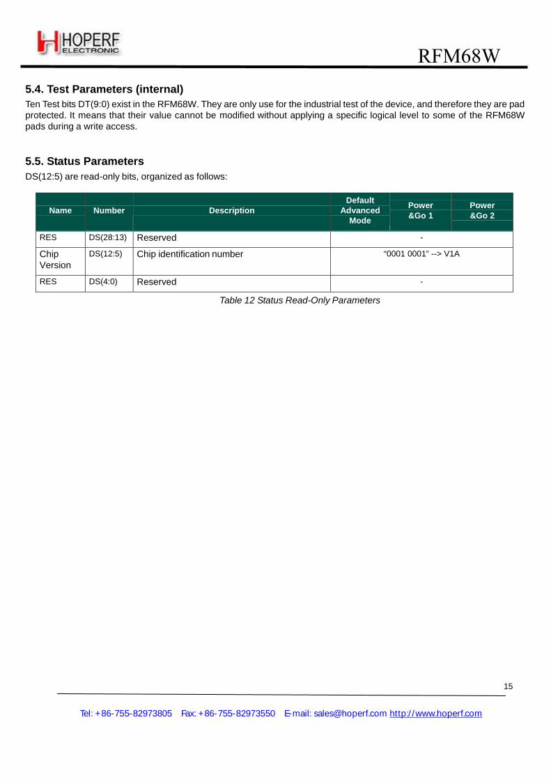
5.5. Status Parameters DS(12:5) are read-only bits, organized as follows:
Name
Number
Description Default
Advanced Mode
Power &Go 1
Power &Go 2
RES DS(28:13) Reserved - Chip Version
DS(12:5) Chip identification number “0001 0001” --> V1A
RES DS(4:0) Reserved -
Table 12 Status Read-Only Parameters
16
RFM68W RFM68W
Tel: +86-755-82973805 Fax: +86-755-82973550 E-mail: [email protected] http:/ /www.hoperf.com
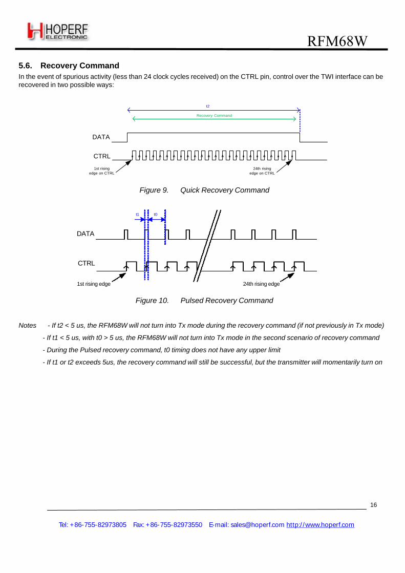
5.6. Recovery Command In the event of spurious activity (less than 24 clock cycles received) on the CTRL pin, control over the TWI interface can be recovered in two possible ways:
t2
Recovery Command
DATA
CTRL
1st rising edge on CTRL
24th rising edge on CTRL
Figure 9. Quick Recovery Command
t1 t0
DATA
CTRL
1st rising edge 24th rising edge
Figure 10. Pulsed Recovery Command Notes - If t2 < 5 us, the RFM68W will not turn into Tx mode during the recovery command (if not previously in Tx mode)
- If t1 < 5 us, with t0 > 5 us, the RFM68W will not turn into Tx mode in the second scenario of recovery command
- During the Pulsed recovery command, t0 timing does not have any upper limit
- If t1 or t2 exceeds 5us, the recovery command will still be successful, but the transmitter will momentarily turn on
17
RFM68W RFM68W
Tel: +86-755-82973805 Fax: +86-755-82973550 E-mail: [email protected] http:/ /www.hoperf.com
6. Application Information
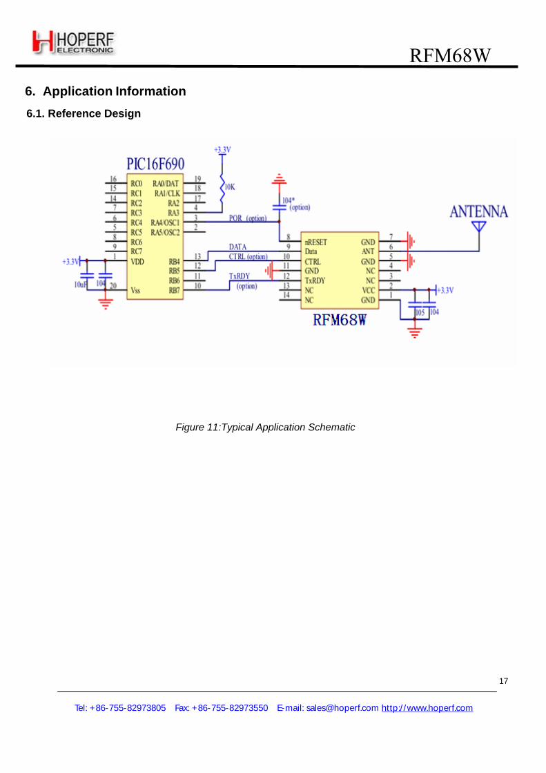
6.1. Reference Design
Figure 11:Typical Application Schematic
18
RFM68W RFM68W
Tel: +86-755-82973805 Fax: +86-755-82973550 E-mail: [email protected] http:/ /www.hoperf.com
6.2. NRESET Pin When required, the pin NRESET can be controlled externally, to allow for:
either a delayed Power On Reset (POR) cycle of the RFM68W, allowing for the companion micro to reset and
assign its
port directions. This is achieved by connecting a R/C time constant to the NRESET pin. or an On-the-go Reset of the RFM68W at any moment in time, if required by the application. This is achieved by
pulling the NRESET pin low for more than 100 microseconds, then releasing it to high impedance (normal termination).
6.3. TX_READY Pin For timing critical applications, TX_READY pin can be useful to know precisely when the transmitter is ready for operation, and therefore save energy. To this end, TX_READY can optionally be connected to inform the companion device that the PA ramp up phase has been terminated, hence the RFM68W is ready for data transmission.
6.4. Low Power Optimization The RFM68W is designed to reduce the cost of the RF transmitter functionnality. To this end, a single DATA signal can be enough to operate the transmitter, in any of the two Power & Go modes. In this situation, TS_START and TOFFT timings, tabulated in Section 2.4, must be respected, leading to significant periods of time during which the transmitter is On and no valuable information is transmitted.
For more demanding applications where energy usage is critical, the RFM68W offers hardware and software support to accurately control the transmitter On time, and therefore save energy:
6.4.1. 2 Connections: CTRL, DATA If the two signals of the TWI interface can be controlled by the host microcontroller, Tx On time can be accurately controlled as follows:
At the device turn on, instead of waiting for TS_TR (2ms max, but very XTAL dependant), the status flag
TX_READY can be polled on the TWI interface. As soon as the TX_READY flag is set, the microcontroller can start toggling DATA
to transmit the useful packet. This method is valid in both Forced Tx and Automatic modes. At the device turn off, instead of waiting for TOFFT (2 or 20ms), the user can immediately turn off the transmitter
after the transmission of packet, assuming that the Forced Transmit mode was selected.
6.4.2. 3 Connections: CTRL, DATA, TX_READY In applications where the number of connections between the microcontroller and the RF module is less critical, TX_READY pin can be connected to either a GPIO port, or an external interrupt port of the micro. The two optimizations described in the former subsection will also be possibl
19
RFM68W RFM68W
Tel: +86-755-82973805 Fax: +86-755-82973550 E-mail: [email protected] http:/ /www.hoperf.com
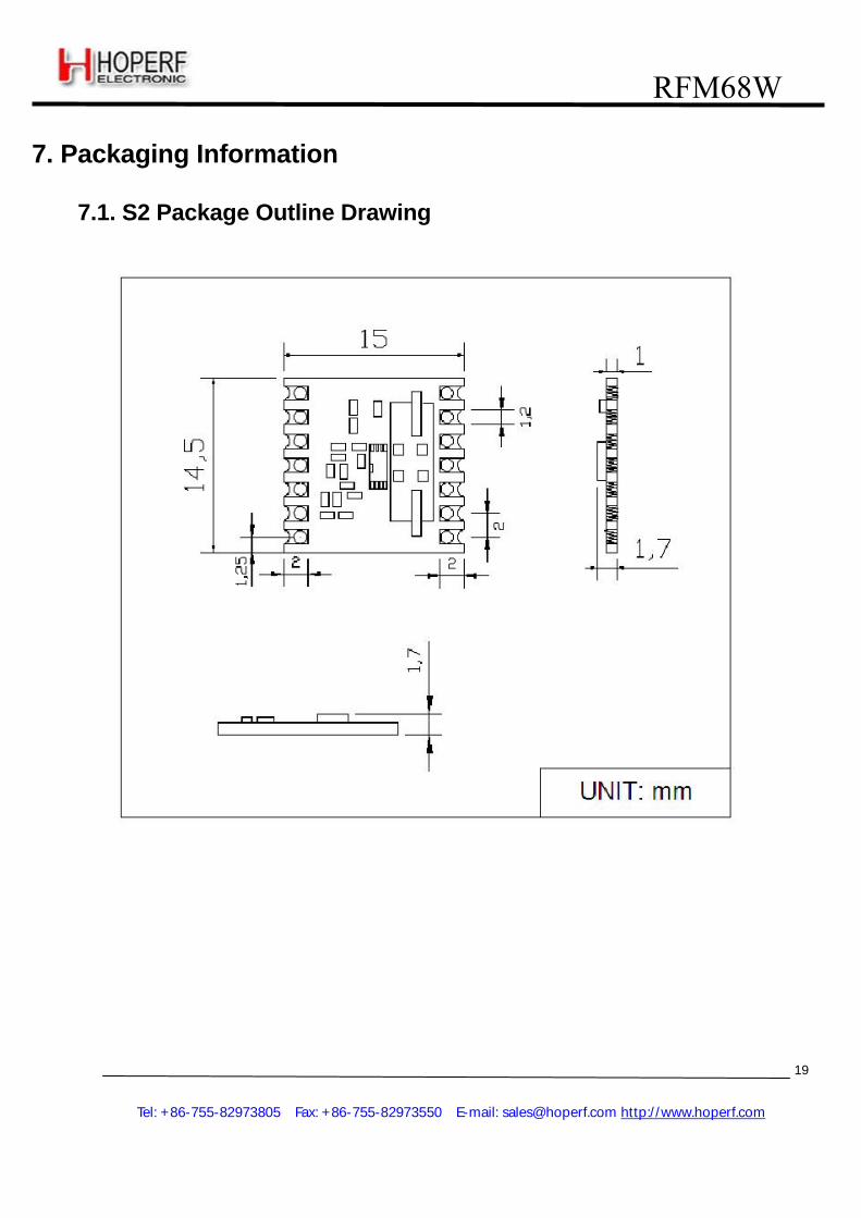
7. Packaging Information
7.1. S2 Package Outline Drawing
RFM68W RF
M68W
Tel: +86-755-82973805 Fax: +86-755-82973550 E-mail: [email protected] http:/ /www.hoperf.com
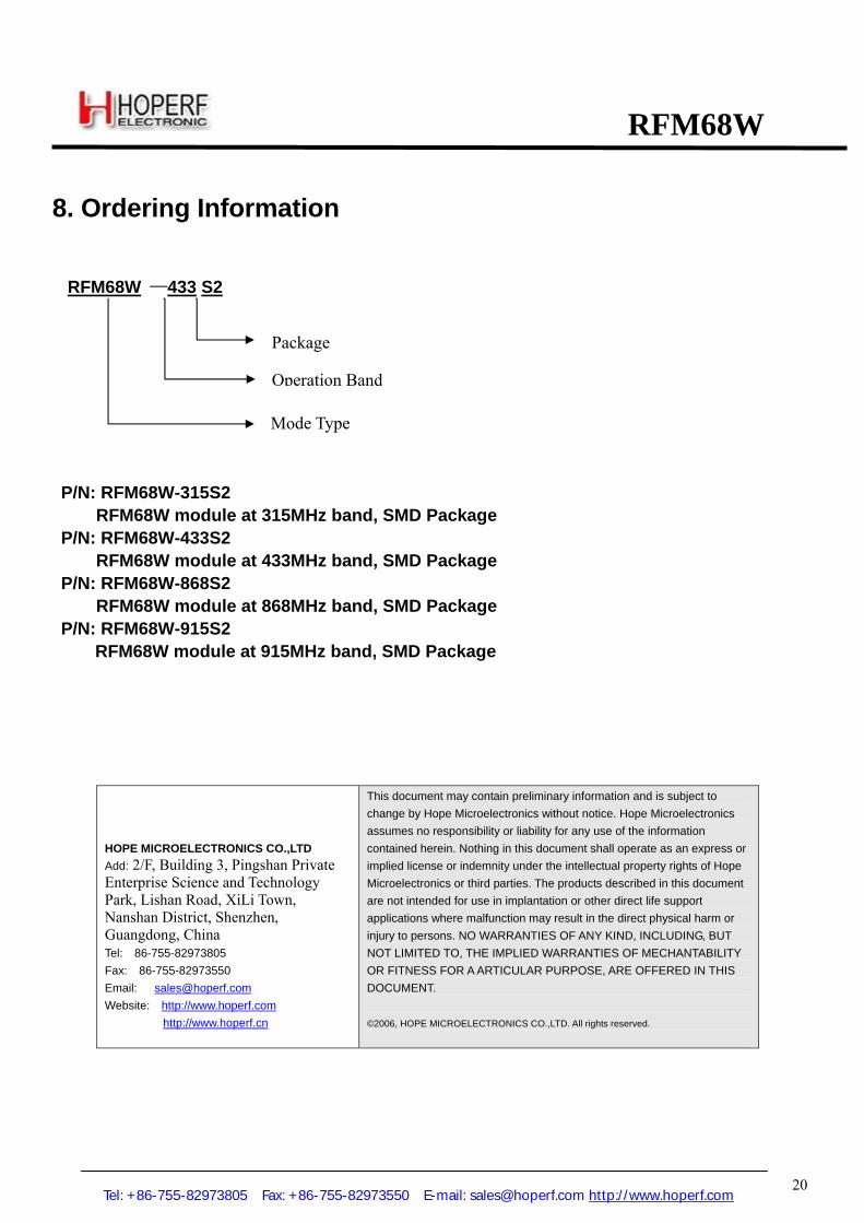
8. Ordering Information
RFM68W —433 S2
P/N: RFM68W-315S2
RFM68W module at 315MHz band, SMD Package P/N: RFM68W-433S2
RFM68W module at 433MHz band, SMD Package P/N: RFM68W-868S2
RFM68W module at 868MHz band, SMD Package P/N: RFM68W-915S2
RFM68W module at 915MHz band, SMD Package
HOPE MICROELECTRONICS CO.,LTD Add: 2/F, Building 3, Pingshan Private Enterprise Science and Technology Park, Lishan Road, XiLi Town, Nanshan District, Shenzhen, Guangdong, China Tel: 86-755-82973805 Fax: 86-755-82973550 Email: [email protected] Website: http://www.hoperf.com http://www.hoperf.cn
This document may contain preliminary information and is subject to change by Hope Microelectronics without notice. Hope Microelectronics assumes no responsibility or liability for any use of the information contained herein. Nothing in this document shall operate as an express or implied license or indemnity under the intellectual property rights of Hope Microelectronics or third parties. The products described in this document are not intended for use in implantation or other direct life support applications where malfunction may result in the direct physical harm or injury to persons. NO WARRANTIES OF ANY KIND, INCLUDING, BUT NOT LIMITED TO, THE IMPLIED WARRANTIES OF MECHANTABILITY OR FITNESS FOR A ARTICULAR PURPOSE, ARE OFFERED IN THIS DOCUMENT. ©2006, HOPE MICROELECTRONICS CO.,LTD. All rights reserved.
RFM68W
20
Package
Operation Band
Mode Type