Embed Size (px)
Citation preview
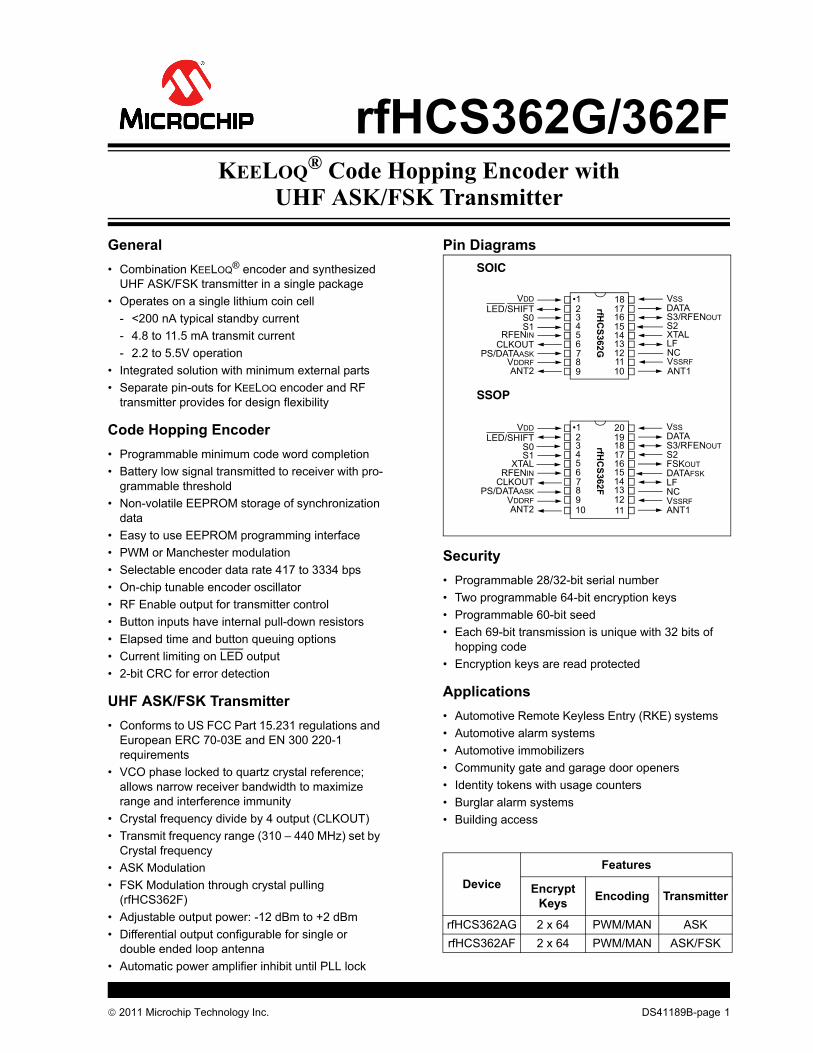
rfHCS362G/362FKEELOQ® Code Hopping Encoder with
UHF ASK/FSK Transmitter
General• Combination KEELOQ® encoder and synthesized
UHF ASK/FSK transmitter in a single package• Operates on a single lithium coin cell
- <200 nA typical standby current- 4.8 to 11.5 mA transmit current- 2.2 to 5.5V operation
• Integrated solution with minimum external parts• Separate pin-outs for KEELOQ encoder and RF
transmitter provides for design flexibility
Code Hopping Encoder• Programmable minimum code word completion• Battery low signal transmitted to receiver with pro-
grammable threshold• Non-volatile EEPROM storage of synchronization
data• Easy to use EEPROM programming interface• PWM or Manchester modulation• Selectable encoder data rate 417 to 3334 bps• On-chip tunable encoder oscillator• RF Enable output for transmitter control• Button inputs have internal pull-down resistors• Elapsed time and button queuing options• Current limiting on LED output• 2-bit CRC for error detection
UHF ASK/FSK Transmitter• Conforms to US FCC Part 15.231 regulations and
European ERC 70-03E and EN 300 220-1 requirements
• VCO phase locked to quartz crystal reference; allows narrow receiver bandwidth to maximize range and interference immunity
• Crystal frequency divide by 4 output (CLKOUT)• Transmit frequency range (310 – 440 MHz) set by
Crystal frequency• ASK Modulation• FSK Modulation through crystal pulling
(rfHCS362F)• Adjustable output power: -12 dBm to +2 dBm• Differential output configurable for single or
double ended loop antenna• Automatic power amplifier inhibit until PLL lock
Pin Diagrams
Security• Programmable 28/32-bit serial number• Two programmable 64-bit encryption keys• Programmable 60-bit seed• Each 69-bit transmission is unique with 32 bits of
hopping code• Encryption keys are read protected
Applications• Automotive Remote Keyless Entry (RKE) systems• Automotive alarm systems• Automotive immobilizers• Community gate and garage door openers• Identity tokens with usage counters• Burglar alarm systems• Building access
DeviceFeatures
Encrypt Keys Encoding Transmitter
rfHCS362AG 2 x 64 PWM/MAN ASKrfHCS362AF 2 x 64 PWM/MAN ASK/FSK
SOIC
VSS
S2XTAL
S3/RFENOUT
VDDLED/SHIFT
S1RFENIN
CLKOUTPS/DATAASK
VDDRF
S0
LF
2 3 4 5 6 7 8 9
•11716
1413121110
15
18 rfHC
S362G
DATA
ANT2
NCVSSRFANT1
SSOP
VSS
S2
DATAFSK
S3/RFENOUT
VDDLED/SHIFT
S1
RFENINCLKOUT
PS/DATAASKVDDRF
S0
LF
2 3 4 5 6 7 8 9
•11918
1615141312
17
20 rfHC
S362F
DATA
NCVSSRF
ANT2 ANT110 11
FSKOUTXTAL
© 2011 Microchip Technology Inc. DS41189B-page 1
rfHCS362G/362F
1.0 GENERAL DESCRIPTIONThe rfHCS362G/362F is a code hopping encoder plusUHF transmitter designed for secure wireless com-mand and control systems. The rfHCS362G/362F uti-lizes the KEELOQ® code hopping technology whichincorporates high security in a small package outline ata low cost to make this device well suited for unidirec-tional remote keyless entry systems and access controlsystems.
The rfHCS362G/362F combines a 32-bit hopping codegenerated by a nonlinear encryption algorithm with a28/32-bit serial number and 9/5 status bits to create a69-bit transmission stream. The length of the transmis-sion strongly resists the threat of code scanning. Thecode hopping mechanism makes each transmissionunique, thus rendering code capture and resend (codegrabbing) schemes virtually useless.
The encryption key, serial number and configurationdata are stored in an EEPROM array which is notaccessible via any external connection. The EEPROMdata is programmable but read protected. The data canbe verified only after an automatic erase and program-ming operation. This protects against attempts to gainaccess to keys or manipulate synchronization values.The rfHCS362G/362F provides an easy to use serialinterface for programming the necessary keys, systemparameters and configuration data.
The transmitter is a fully integrated UHF ASK/FSKtransmitter consisting of crystal oscillator, Phase-Locked Loop (PLL), open-collector differential-outputPower Amplifier (PA), and mode control logic. Externalcomponents consist of bypass capacitors, crystal, andPLL loop filter. There are no internal electrical connec-tions between the encoder and the transmitter. Theencoder oscillator is independent from the transmittercrystal oscillator.
The rfHCS362G is capable of Amplitude Shift Keying(ASK) modulation by turning the PA on and off. TherfHCS362F is capable of ASK or Frequency Shift Key-ing (FSK) modulation by employing an internal FSKswitch to pull the transmitter crystal via a second loadcapacitor.
The rfHCS362G/362F is a single channel device. Thetransmit frequency is fixed and set by an external refer-ence crystal. Transmit frequencies in the range of 310to 440 MHz can be selected. Output drive is an open-collector differential amplifier. The differential output iswell suited for loop antennas. Output power is adjust-able from +2 dBm to -12 dBm in six discrete steps.
The rfHCS362G/362F are radio frequency (RF) emit-ting devices. Wireless RF devices are governed by acountry’s regulating agency. For example, in the UnitedStates it is the Federal Communications Committee(FCC) and in Europe it is the European Conference ofPostal and Telecommunications Administrations
(CEPT). It is the responsibility of the designer to ensurethat their end product conforms to rules and regulationsof the country of use and/or sale.
RF devices require correct board level implementationin order to meet regulatory requirements. Layout con-siderations are given in Section 6.0 UHF ASK/FSKTransmitter.
1.1 Important TermsThe following is a list of key terms used throughout thisdata sheet. For additional information on KEELOQ andCode Hopping refer to Technical Brief 3 (TB003).
• RKE - Remote Keyless Entry• Button Status - Indicates what button input(s)
activated the transmission. Encompasses the 4 button status bits S3, S2, S1 and S0 (Figure 3-6).
• Code Hopping - A method by which a code, viewed externally to the system, appears to change unpredictably each time it is transmitted.
• Code word - A block of data that is repeatedly transmitted upon button activation (Figure 3-6).
• Transmission - A data stream consisting of repeating code words (Figure 10-1).
• Encryption key - A unique and secret 64-bit number used to encrypt and decrypt data. In a symmetrical block cipher such as the KEELOQ algorithm, the encryption and decryption keys are equal and will be referred to generally as the encryption key.
• Encoder - A device that generates and encodes data.
• Encryption Algorithm - A recipe whereby data is scrambled using a encryption key. The data can only be interpreted by the respective decryption algorithm using the same encryption key.
• Decoder - A device that decodes data received from an encoder.
• Decryption algorithm - A recipe whereby data scrambled by an encryption algorithm can be unscrambled using the same encryption key.
• Learn – Learning involves the receiver calculating the transmitter’s appropriate encryption key, decrypting the received hopping code and storing the serial number, synchronization counter value and encryption key in EEPROM. The KEELOQ product family facilitates several learning strate-gies to be implemented on the decoder. The fol-lowing are examples of what can be done. - Simple Learning
The receiver uses a fixed encryption key, common to all components of all systems by the same manufacturer, to decrypt the received code word’s encrypted portion.
DS41189B-page 2 © 2011 Microchip Technology Inc.
rfHCS362G/362F
- Normal LearningThe receiver uses information transmitted during normal operation to derive the encryp-tion key and decrypt the received code word’s encrypted portion.
- Secure LearnThe transmitter is activated through a special button combination to transmit a stored 60-bit seed value used to generate the transmitter’s encryption key. The receiver uses this seed value to derive the same encryption key and decrypt the received code word’s encrypted portion.
• Manufacturer’s code – A unique and secret 64-bit number used to generate unique encoder encryption keys. Each encoder is programmed with a encryption key that is a function of the man-ufacturer’s code. Each decoder is programmed with the manufacturer code itself.
1.2 ApplicationsThe rfHCS362G/362F is suited for secure wirelessremote control applications. The EEPROM technologymakes customizing application programs (transmittercodes, appliance settings, etc.) extremely fast and con-venient. The small footprint packages are suitable forapplications with space limitations. Low-cost, low-power, high performance, ease of use and I/O flexibilitymake the rfHCS362G/362F very versatile. Typicalapplication circuits are shown in Figure 1-5 andFigure 1-6.
Most low-end keyless entry transmitters are given afixed identification code that is transmitted every time abutton is pushed. The number of unique identificationcodes in a low-end system is usually a relatively smallnumber. These shortcomings provide an opportunityfor a sophisticated thief to create a device that ‘grabs’a transmission and retransmits it later, or a device thatquickly ‘scans’ all possible identification codes until thecorrect one is found.
The rfHCS362G/362F, on the other hand, employs theKEELOQ code hopping technology coupled with a trans-mission length of 66 bits to virtually eliminate the use ofcode ‘grabbing’ or code ‘scanning’. The high securitylevel of the rfHCS362G/362F is based on patentedtechnology. A block cipher based on a block length of32 bits and a key length of 64 bits is used. The algo-rithm obscures the information in such a way that evenif the transmission information (before coding) differsby only one bit from that of the previous transmission,the next coded transmission will be completely differ-ent. Statistically, if only one bit in the 32-bit string ofinformation changes, approximately 50 percent of thecoded transmission bits will change.
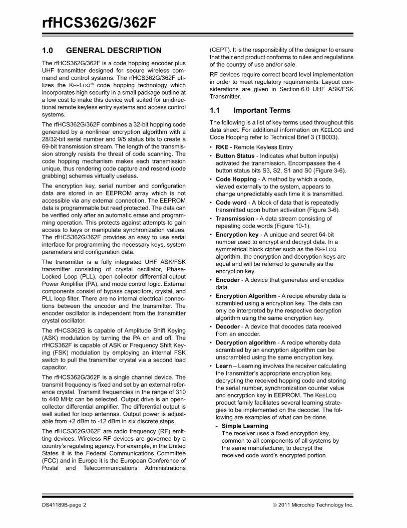
FIGURE 1-1: ADDITIONAL BUTTON INPUTS
Up to 7 button inputs can be implemented making themlook like a binary value to the 3 Sx inputs. This is donewith switching diodes as shown in Figure 1-1. The dis-advantage is that simultaneously pressed buttons nowappear as if a single button is pressed.
The rfHCS362G/362F has a small EEPROM arraywhich must be loaded with several parameters beforeuse. These are most often programmed by the manu-facturer at the time of production. The most importantof these are:
• A 28-bit serial number, typically unique for every encoder
• An encryption key• An initial 16-bit synchronization value• A 16-bit configuration value
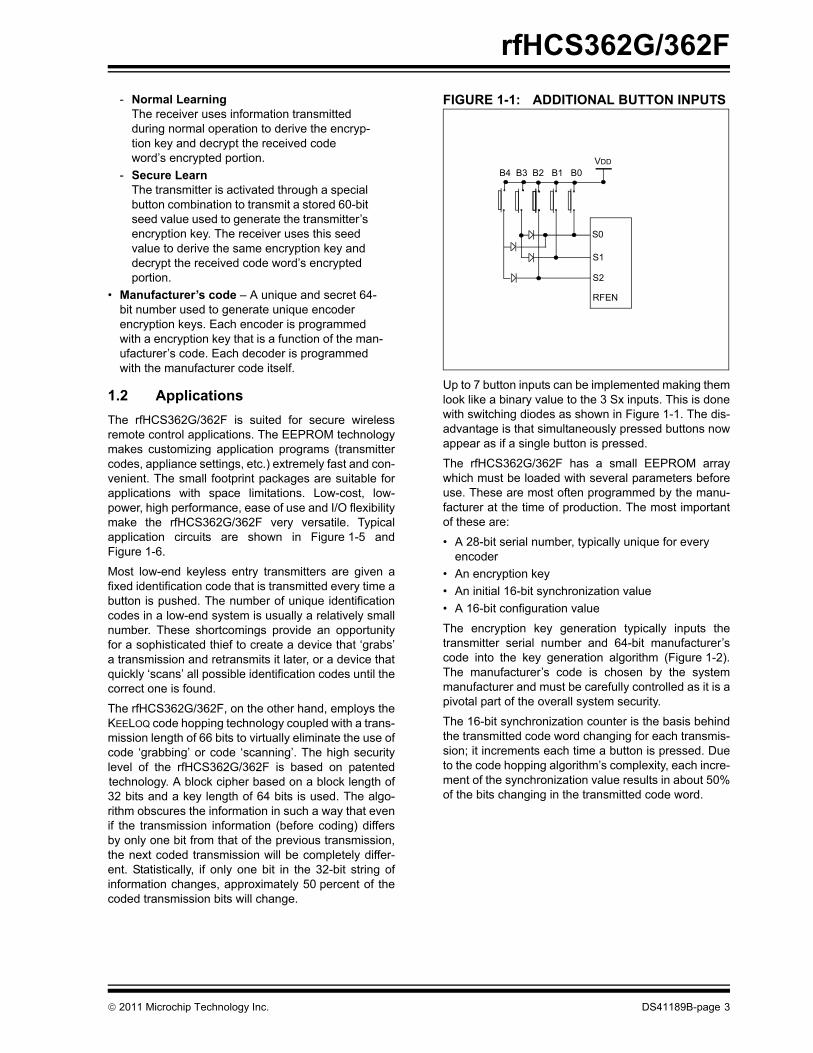
The encryption key generation typically inputs thetransmitter serial number and 64-bit manufacturer’scode into the key generation algorithm (Figure 1-2).The manufacturer’s code is chosen by the systemmanufacturer and must be carefully controlled as it is apivotal part of the overall system security.
The 16-bit synchronization counter is the basis behindthe transmitted code word changing for each transmis-sion; it increments each time a button is pressed. Dueto the code hopping algorithm’s complexity, each incre-ment of the synchronization value results in about 50%of the bits changing in the transmitted code word.
VDD
S0
S1
S2
RFEN
B4 B3 B2 B1 B0
© 2011 Microchip Technology Inc. DS41189B-page 3
rfHCS362G/362F
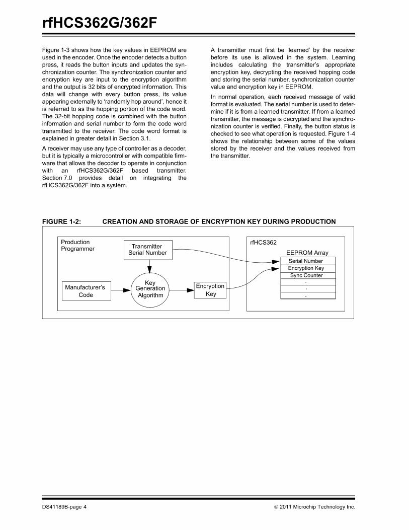
Figure 1-3 shows how the key values in EEPROM areused in the encoder. Once the encoder detects a buttonpress, it reads the button inputs and updates the syn-chronization counter. The synchronization counter andencryption key are input to the encryption algorithmand the output is 32 bits of encrypted information. Thisdata will change with every button press, its valueappearing externally to ‘randomly hop around’, hence itis referred to as the hopping portion of the code word.The 32-bit hopping code is combined with the buttoninformation and serial number to form the code wordtransmitted to the receiver. The code word format isexplained in greater detail in Section 3.1.A receiver may use any type of controller as a decoder,but it is typically a microcontroller with compatible firm-ware that allows the decoder to operate in conjunctionwith an rfHCS362G/362F based transmitter.Section 7.0 provides detail on integrating therfHCS362G/362F into a system.
A transmitter must first be ‘learned’ by the receiverbefore its use is allowed in the system. Learningincludes calculating the transmitter’s appropriateencryption key, decrypting the received hopping codeand storing the serial number, synchronization countervalue and encryption key in EEPROM.
In normal operation, each received message of validformat is evaluated. The serial number is used to deter-mine if it is from a learned transmitter. If from a learnedtransmitter, the message is decrypted and the synchro-nization counter is verified. Finally, the button status ischecked to see what operation is requested. Figure 1-4shows the relationship between some of the valuesstored by the receiver and the values received fromthe transmitter.
FIGURE 1-2: CREATION AND STORAGE OF ENCRYPTION KEY DURING PRODUCTION
Transmitter
Manufacturer’s
Serial Number
CodeEncryption
Key
KeyGenerationAlgorithm
Serial NumberEncryption KeySync Counter
..
.
rfHCS362ProductionProgrammer
EEPROM Array
DS41189B-page 4 © 2011 Microchip Technology Inc.
rfHCS362G/362F
FIGURE 1-3: BUILDING THE TRANSMITTED CODE WORD (ENCODER)FIGURE 1-4: BASIC OPERATION OF RECEIVER (DECODER)
NOTE: Circled numbers indicate the order of execution.
Button PressInformation
EEPROM Array
32 Bits Encrypted DataSerial Number
Transmitted Information
Encryption Key
Sync Counter
Serial Number
KEELOQ®
EncryptionAlgorithm
Button Press Information
EEPROM Array
Manufacturer Code 32 Bits of Encrypted DataSerial Number
Received Information
DecryptedSynchronization Counter
Check for Match
Sync Counter
Serial Number
KEELOQ®
DecryptionAlgorithm
1
3
4
Check for Match2
Perform Function Indicated by button press 5
Encryption Key
© 2011 Microchip Technology Inc. DS41189B-page 5
rfHCS362G/362F
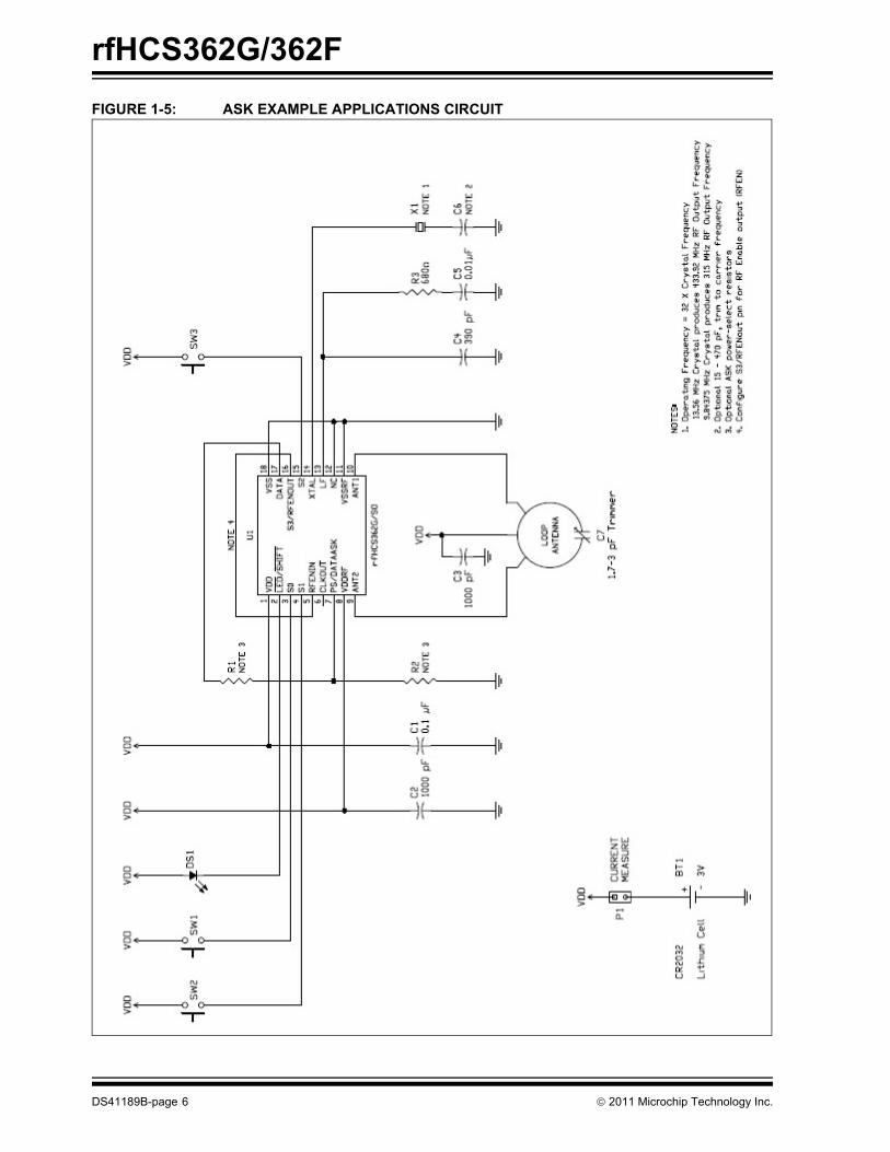
FIGURE 1-5: ASK EXAMPLE APPLICATIONS CIRCUITDS41189B-page 6 © 2011 Microchip Technology Inc.
rfHCS362G/362F
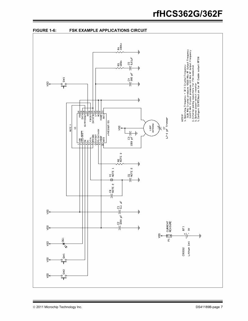
FIGURE 1-6: FSK EXAMPLE APPLICATIONS CIRCUIT© 2011 Microchip Technology Inc. DS41189B-page 7
rfHCS362G/362F
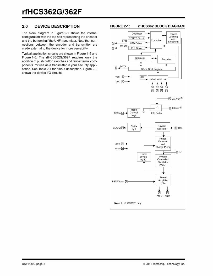
2.0 DEVICE DESCRIPTIONThe block diagram in Figure 2-1 shows the internalconfiguration with the top half representing the encoderand the bottom half the UHF transmitter. Note that con-nections between the encoder and transmitter aremade external to the device for more versability.
Typical application circuits are shown in Figure 1-5 andFigure 1-6. The rfHCS362G/362F requires only theaddition of push button switches and few external com-ponents for use as a transmitter in your security appli-cation. See Table 2-1 for pinout description. Figure 2-2shows the device I/O circuits.
FIGURE 2-1: rfHCS362 BLOCK DIAGRAM
VSS
VDD
Oscillator
RESET Circuit
LED DriverController
PowerLatching
andSwitching
Button Input Port
32-bit Shift Register
EncoderEEPROM
DATA
LED
S3 S2 S1 S0
SHIFT
PLL DriverRFEN
RFENIN
Divideby 4
ModeControlLogic
CLKOUT
PowerAmplifier
(PA)
CrystalOscillator
ANT2 ANT1
XTAL
Phase Detector
andCharge Pump
Voltage Controlled Oscillator
(VCO)
Fixed Divideby 32
LF
PS/DATAASK
DATAFSK (1)
FSKOUT (1)
FSK Switch
VDDRF
VSSRF
Note 1: rfHCS362F only.
DS41189B-page 8 © 2011 Microchip Technology Inc.
rfHCS362G/362F
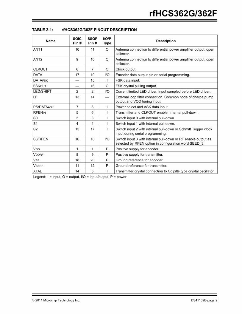
TABLE 2-1: rfHCS362G/362F PINOUT DESCRIPTIONName SOICPin #
SSOP Pin #
I/O/P Type Description
ANT1 10 11 O Antenna connection to differential power amplifier output, open collector.
ANT2 9 10 O Antenna connection to differential power amplifier output, open collector.
CLKOUT 6 7 O Clock output.DATA 17 19 I/O Encoder data output pin or serial programming.DATAFSK — 15 I FSK data input.FSKOUT — 16 O FSK crystal pulling output.LED/SHIFT 2 2 I/O Current limited LED driver. Input sampled before LED driven.LF 13 14 — External loop filter connection. Common node of charge pump
output and VCO tuning input.PS/DATAASK 7 8 I Power select and ASK data input.RFENIN 5 6 I Transmitter and CLKOUT enable. Internal pull-down.S0 3 3 I Switch input 0 with internal pull-down.S1 4 4 I Switch input 1 with internal pull-down.S2 15 17 I Switch input 2 with internal pull-down or Schmitt Trigger clock
input during serial programming.S3/RFEN 16 18 I/O Switch input 3 with internal pull-down or RF enable output as
selected by RFEN option in configuration word SEED_3.VDD 1 1 P Positive supply for encoderVDDRF 8 9 P Positive supply for transmitter.VSS 18 20 P Ground reference for encoderVSSRF 11 12 P Ground reference for transmitter.XTAL 14 5 I Transmitter crystal connection to Colpitts type crystal oscillator.Legend: I = input, O = output, I/O = input/output, P = power
© 2011 Microchip Technology Inc. DS41189B-page 9
rfHCS362G/362F
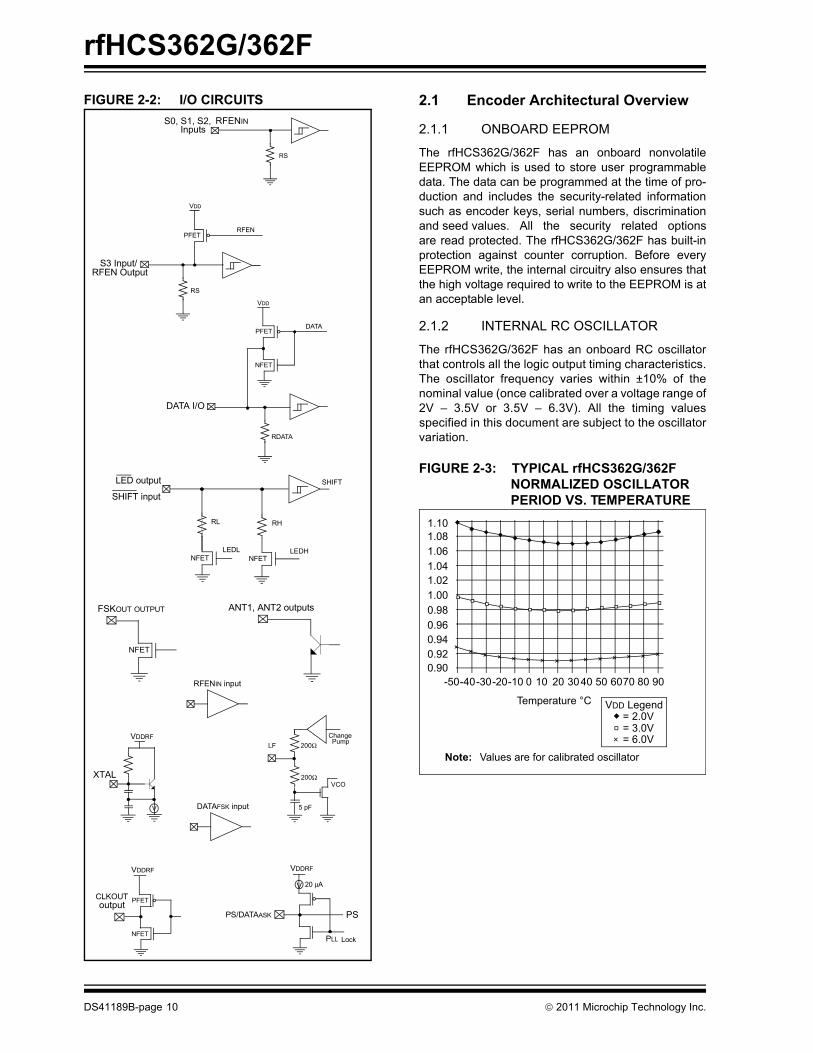
FIGURE 2-2: I/O CIRCUITS 2.1 Encoder Architectural Overview2.1.1 ONBOARD EEPROM
The rfHCS362G/362F has an onboard nonvolatileEEPROM which is used to store user programmabledata. The data can be programmed at the time of pro-duction and includes the security-related informationsuch as encoder keys, serial numbers, discriminationand seed values. All the security related optionsare read protected. The rfHCS362G/362F has built-inprotection against counter corruption. Before everyEEPROM write, the internal circuitry also ensures thatthe high voltage required to write to the EEPROM is atan acceptable level.
2.1.2 INTERNAL RC OSCILLATOR
The rfHCS362G/362F has an onboard RC oscillatorthat controls all the logic output timing characteristics.The oscillator frequency varies within ±10% of thenominal value (once calibrated over a voltage range of2V – 3.5V or 3.5V – 6.3V). All the timing valuesspecified in this document are subject to the oscillatorvariation.
FIGURE 2-3: TYPICAL rfHCS362G/362F NORMALIZED OSCILLATOR PERIOD VS. TEMPERATURE
S0, S1, S2,
RS
Inputs
VDD
RFEN
S3 Input/
RS
RDATA
DATA I/O
LED output
RL RH
VDD
DATA
LEDHLEDL
RFEN Output
PFET
NFET
PFET
NFETNFET
SHIFT inputSHIFT
RFENIN
NFET
FSKOUT OUTPUT ANT1, ANT2 outputs
CLKOUT
VDDRF
PFET
NFET
PS/DATAASK
VDDRF
V
PLL Lock
20 μA
VDDRF
V
VCO
5 pF
200Ω
200Ω
ChangePumpLF
RFENIN input
XTAL
outputPS
DATAFSK input
0.94
1.101.081.061.041.021.000.980.96
0.920.90
VDD Legend= 2.0V= 3.0V= 6.0V
Temperature °C
-50-40-30-20-10 0 10 20 3040 50 6070 80 90
Note: Values are for calibrated oscillator
DS41189B-page 10 © 2011 Microchip Technology Inc.
rfHCS362G/362F
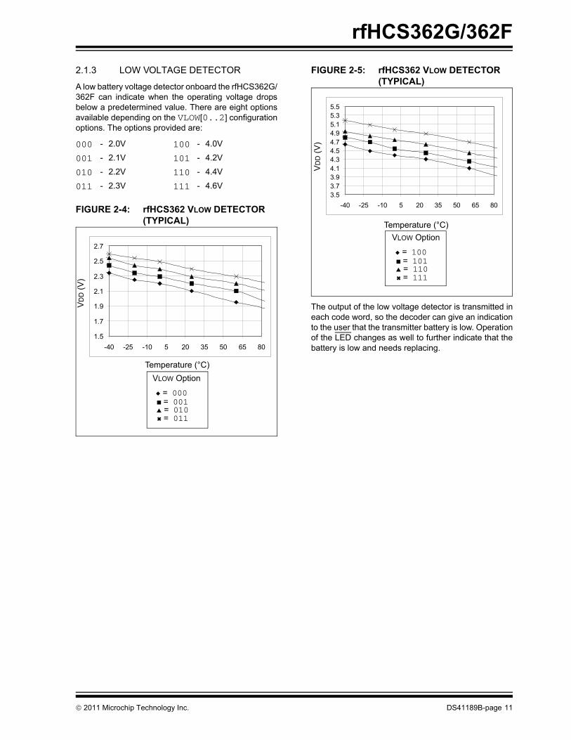
2.1.3 LOW VOLTAGE DETECTORA low battery voltage detector onboard the rfHCS362G/362F can indicate when the operating voltage dropsbelow a predetermined value. There are eight optionsavailable depending on the VLOW[0..2] configurationoptions. The options provided are:
FIGURE 2-4: rfHCS362 VLOW DETECTOR (TYPICAL)
FIGURE 2-5: rfHCS362 VLOW DETECTOR (TYPICAL)
The output of the low voltage detector is transmitted ineach code word, so the decoder can give an indicationto the user that the transmitter battery is low. Operationof the LED changes as well to further indicate that thebattery is low and needs replacing.
000 - 2.0V 100 - 4.0V
001 - 2.1V 101 - 4.2V
010 - 2.2V 110 - 4.4V
011 - 2.3V 111 - 4.6V
1.5
1.7
1.9
2.1
2.3
2.5
2.7
-40 -25 -10 5 20 35 50 65 80
VD
D (V
)
Temperature (°C)VLOW Option
◆ = 000■ = 001▲ = 010✖ = 011
VD
D (V
)
Temperature (°C)
3.53.73.94.14.34.54.74.95.15.35.5
-40 -25 -10 5 20 35 50 65 80
VLOW Option
◆ = 100■ = 101▲ = 110✖ = 111
© 2011 Microchip Technology Inc. DS41189B-page 11
rfHCS362G/362F
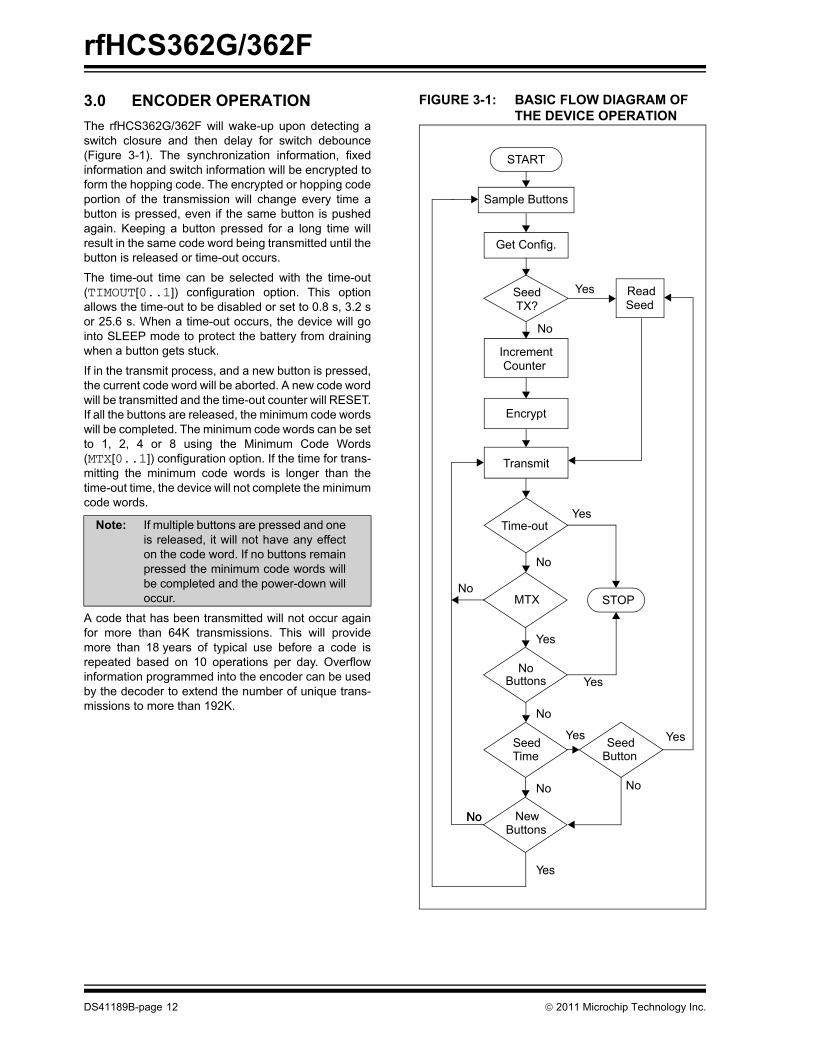
3.0 ENCODER OPERATIONThe rfHCS362G/362F will wake-up upon detecting aswitch closure and then delay for switch debounce(Figure 3-1). The synchronization information, fixedinformation and switch information will be encrypted toform the hopping code. The encrypted or hopping codeportion of the transmission will change every time abutton is pressed, even if the same button is pushedagain. Keeping a button pressed for a long time willresult in the same code word being transmitted until thebutton is released or time-out occurs.
The time-out time can be selected with the time-out(TIMOUT[0..1]) configuration option. This optionallows the time-out to be disabled or set to 0.8 s, 3.2 sor 25.6 s. When a time-out occurs, the device will gointo SLEEP mode to protect the battery from drainingwhen a button gets stuck.
If in the transmit process, and a new button is pressed,the current code word will be aborted. A new code wordwill be transmitted and the time-out counter will RESET.If all the buttons are released, the minimum code wordswill be completed. The minimum code words can be setto 1, 2, 4 or 8 using the Minimum Code Words(MTX[0..1]) configuration option. If the time for trans-mitting the minimum code words is longer than thetime-out time, the device will not complete the minimumcode words.
A code that has been transmitted will not occur againfor more than 64K transmissions. This will providemore than 18 years of typical use before a code isrepeated based on 10 operations per day. Overflowinformation programmed into the encoder can be usedby the decoder to extend the number of unique trans-missions to more than 192K.
FIGURE 3-1: BASIC FLOW DIAGRAM OF THE DEVICE OPERATION
Note: If multiple buttons are pressed and oneis released, it will not have any effecton the code word. If no buttons remainpressed the minimum code words willbe completed and the power-down willoccur.
START
Sample Buttons
Increment
Seed
Time-out
Encrypt
No
No
Yes
Get Config.
TX?
Counter
Transmit
MTX
NoButtons
SeedTime
ReadSeed
STOP
Yes
Yes
No
Yes
No
No
Yes
YesYes SeedButton
No
NewButtons
NoNo
DS41189B-page 12 © 2011 Microchip Technology Inc.
rfHCS362G/362F
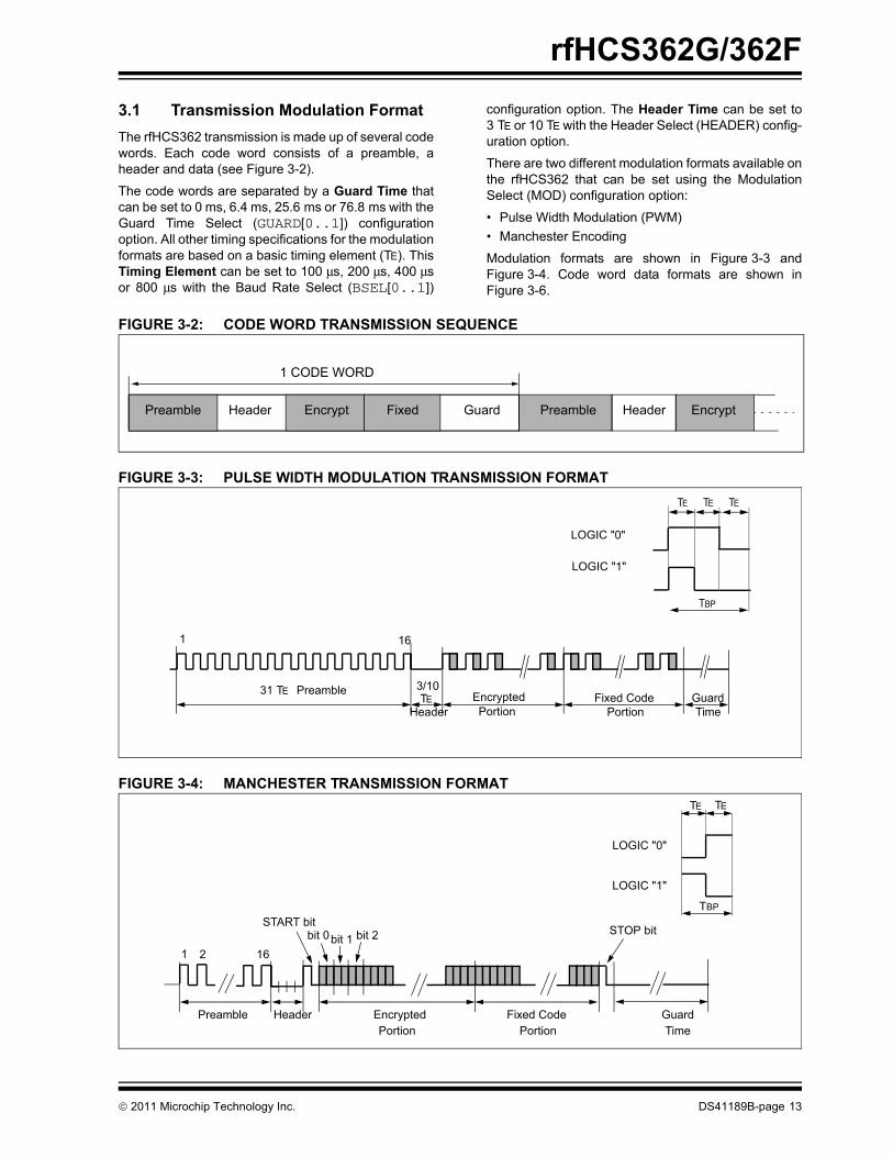
3.1 Transmission Modulation FormatThe rfHCS362 transmission is made up of several codewords. Each code word consists of a preamble, aheader and data (see Figure 3-2).The code words are separated by a Guard Time thatcan be set to 0 ms, 6.4 ms, 25.6 ms or 76.8 ms with theGuard Time Select (GUARD[0..1]) configurationoption. All other timing specifications for the modulationformats are based on a basic timing element (TE). ThisTiming Element can be set to 100 μs, 200 μs, 400 μsor 800 μs with the Baud Rate Select (BSEL[0..1])
configuration option. The Header Time can be set to3 TE or 10 TE with the Header Select (HEADER) config-uration option.
There are two different modulation formats available onthe rfHCS362 that can be set using the ModulationSelect (MOD) configuration option:
• Pulse Width Modulation (PWM)• Manchester Encoding
Modulation formats are shown in Figure 3-3 andFigure 3-4. Code word data formats are shown inFigure 3-6.
FIGURE 3-2: CODE WORD TRANSMISSION SEQUENCE
FIGURE 3-3: PULSE WIDTH MODULATION TRANSMISSION FORMAT
FIGURE 3-4: MANCHESTER TRANSMISSION FORMAT
Header Encrypt Fixed Guard
1 CODE WORD
Preamble EncryptPreamble Header
LOGIC "1"
GuardTime
31 TE EncryptedPortion
Fixed Code Portion
LOGIC "0"
Preamble 3/10
Header
TE TE TE
TE
1 16
TBP
GuardPreamble Header Encrypted Fixed Code
1 2
START bitSTOP bit
TimePortion Portion
16 bit 0 bit 1 bit 2
LOGIC "0"
LOGIC "1"
TE TE
TBP
© 2011 Microchip Technology Inc. DS41189B-page 13
rfHCS362G/362F
3.1.1 CODE HOPPING DATAThe hopping portion is calculated by encrypting thecounter, discrimination value and function code with theEncoder Key (KEY). The counter is 16 bits wide. Thediscrimination value is 10 bits wide. There are 2 coun-ter overflow bits (OVR) that are cleared when the coun-ter wraps to 0. The rest of the 32 bits are made up ofthe function code also known as the button inputs.
3.1.2 FIXED CODE DATA
The 32 bits of fixed code consist of 28 bits of the serialnumber (SER) and another copy of the function code.This can be changed to contain the whole 32-bit serialnumber with the Extended Serial Number (XSER) con-figuration option.
3.1.3 MINIMUM CODE WORDS
MTX[0..1] configuration bits selects the minimumnumber of code words that will be transmitted. If thebutton is released after 1.6 s (or greater) and MTX codewords have been transmitted, the code word beingtransmitted will be terminated. The possible values are:
00 - 1
01 - 2
10 - 4
11 - 8
3.1.4 STATUS INFORMATION
The status bits will always contain the output of the LowVoltage detector (VLOW), the Cyclic RedundancyCheck (CRC) bits (or TIME bits depending on CTSEL)and the Button Queue information.
3.1.4.1 Low Voltage Detector Status (VLOW)The output of the low voltage detector is transmittedwith each code word. If VDD drops below the selectedvoltage, a logic ‘1’ will be transmitted. The output of thedetector is sampled before each code word is transmit-ted.
DS41189B-page 14 © 2011 Microchip Technology Inc.
rfHCS362G/362F
3.1.4.2 Button Queue Information (QUEUE)The queue bits indicate a button combination waspressed again within 2 s after releasing the previousactivation. Queuing or repeated pressing of the samebuttons (or button combination) is detected by therfHCS362 button debouncing circuitry.The Queue bits are added as the last two bits of thestandard code word. The queue bits are a 2-bit counterthat does not wrap. The counter value starts at ‘00b’and is incremented if a button is pushed within 2 s ofthe previous button press. The current code word is ter-minated when the buttons are queued. This allowsadditional functionality for repeated button presses.
The button inputs are sampled every 6.4 ms during this2 s period.
00 - first activation
01 - second activation
10 - third activation
11 - from fourth activation on
3.1.4.3 Time BITSThe time bits (Figure 3-5) indicate the duration that theinputs were activated:
00 - immediate01 - after 0.8 s10 - after 1.6 s11 - after 2.4 s
The TIME bits are incremented every 0.8 s and will notwrap once it reaches ‘11’.
Time information is alternative to the CRC bits availabil-ity and is selected by the CTSEL configuration bit.
FIGURE 3-5: TIME BITS OPERATION
3.1.4.4 Cyclic Redundancy Check (CRC)The CRC bits are calculated on the 65 previously trans-mitted bits. The decoder can use the CRC bits to checkthe data integrity before processing starts. The CRCcan detect all single bit errors and 66% of double biterrors. The CRC is computed as follows:
EQUATION 3-1: CRC Calculation
and
with
and Din the nth transmission bit 0 ≤ n ≤ 64
TTD
Time
DATA
= One Code Word
Time bits = 00 Time bits set internally to 01
Time bits actually output
Time bits set internally to 10
Time bits actually output
0 s 0.8 s 1.6 s 2.4 s
S[3210]
CRC 1[ ]n 1+ CRC 0[ ]n Din⊕=
CRC 0[ ]n 1+ CRC 0[ ]n Din⊕( ) CRC 1[ ]n⊕=
CRC 1 0,[ ]0 0=
Warning: The CRC may be wrong when the batteryvoltage is near the selected VLOW trip point.This may happen because VLOW is sam-pled twice each transmission, once for theCRC calculation and once when VLOW istransmitted. VDD tends to move slightly dur-ing a transmission which could lead to a dif-ferent value for VLOW being used for theCRC calculation and the transmission.
Work around: If the CRC is incorrect,recalculate for the opposite value of VLOW.
© 2011 Microchip Technology Inc. DS41189B-page 15
rfHCS362G/362F
FIGURE 3-6: CODE WORD DATA FORMATTransmission Direction LSB First
Fixed Portion (32 bits)
QUE2 bits
CRC2 bits
VLOW1-bit
SERIAL NUMBER(32 bits)
Q1 Q0 C1 C0
BUT4 bits
CounterOverflow
2 bitsDISC10 bits
Synchronization
16 bitsCounter
15 0
S2 S1 S0 S3 OVR1 OVR0
Encrypted Portion (32 bits)
With XSER = 1, CTSEL = 0
Status Information(5 bits)
Fixed Portion (32 bits)
QUE2 bits
TIME2 bits
VLOW1-bit
SERIAL NUMBER(28 bits)
Q1 Q0 T1 T0 S2 S1 S0 S3
With XSER = 1, CTSEL = 1
Status Information(5 bits)
BUT4 bits
BUT4 bits
CounterOverflow
2 bitsDISC10 bits
Synchronization
16 bitsCounter
15 0
S2 S1 S0 S3 OVR1 OVR0
Encrypted Portion (32 bits)
Fixed Code Portion (32 bits)
QUE2 bits
CRC2 bits
VLOW1-bit
SERIAL NUMBER(28 bits)
Q1 Q0 C1 C0 S2 S1 S0 S3
Status Information(5 bits)
BUT4 bits
BUT4 bits
CounterOverflow
2 bitsDISC10 bits
Synchronization
16 bitsCounter
15 0
S2 S1 S0 S3 OVR1 OVR0
Encrypted Portion (32 bits)
With XSER = 0, CTSEL = 0
Fixed Portion (32 bits)
QUE2 bits
TIME2 bits
VLOW1-bit
SERIAL NUMBER(32 bits)
Q1 Q0 T1 T0
BUT4 bits
CounterOverflow
2 bitsDISC10 bits
Synchronization
16 bitsCounter
15 0
S2 S1 S0 S3 OVR1 OVR0
Encrypted Portion (32 bits)Status Information(5 bits)
With XSER = 0, CTSEL = 1
DS41189B-page 16 © 2011 Microchip Technology Inc.
rfHCS362G/362F
3.2 LED OutputThe LED pin will be driven LOW periodically while therfHCS362 is transmitting data to power an externalLED.The duty cycle (TLEDON/TLEDOFF) can be selectedbetween two possible values by the configurationoption (LED).
FIGURE 3-7: LED OPERATION (LED = 1)
The same configuration option determines whetherwhen the VDD Voltage drops below the selected VLOWtrip point the LED will blink only once or stop blinking.
FIGURE 3-8: LED OPERATION (LED = 0)
3.3 Dual Encoder OperationThe rfHCS362G/362F contains two encryption keys(for example derived from two different Manufacturer’sCodes), but only one Serial Number, one set of Dis-crimination bits, one 16-bit Synchronization Counterand a single 60-bit Seed value. For this reason therfHCS362G/362F can be used as an encoder in multi-ple (two) applications as far as they share the sameconfiguration: transmission format, baud rate, headerand guard settings. The SHIFT input pin (multiplexedwith the LED output) is used to select between the twoencryption keys.
A logic 1 on the SHIFT input pin selects the first encryp-tion key.
A logic 0 on the SHIFT input pin will select the secondencryption key.
FIGURE 3-9: USING DUAL ENCODER OPERATION
Note: When the rfHCS362 encoder is usedas a Dual Encoder the LED pin is usedas a SHIFT input (Figure 3-9). In sucha configuration the LED is always ONduring transmission. To keep powerconsumption low, it is recommendedto use a series resistor of relativelyhigh value. VLOW information is notavailable when using the secondEncryption Key.
S[3210]
LED
VDD > VLOW
TLEDON = 25 ms
TLEDOFF
LED
VDD < VLOW
TLEDON
TLEDOFF = 500 ms
LED
VDD < VLOW
S[3210]
LED
VDD > VLOW TLEDON TLEDOFF
TLEDON = 200 ms TLEDOFF = 800 ms
VDD
VDD
DATA
VSS
SHIFT
1 kΩ
LED/SHIFT
© 2011 Microchip Technology Inc. DS41189B-page 17
rfHCS362G/362F
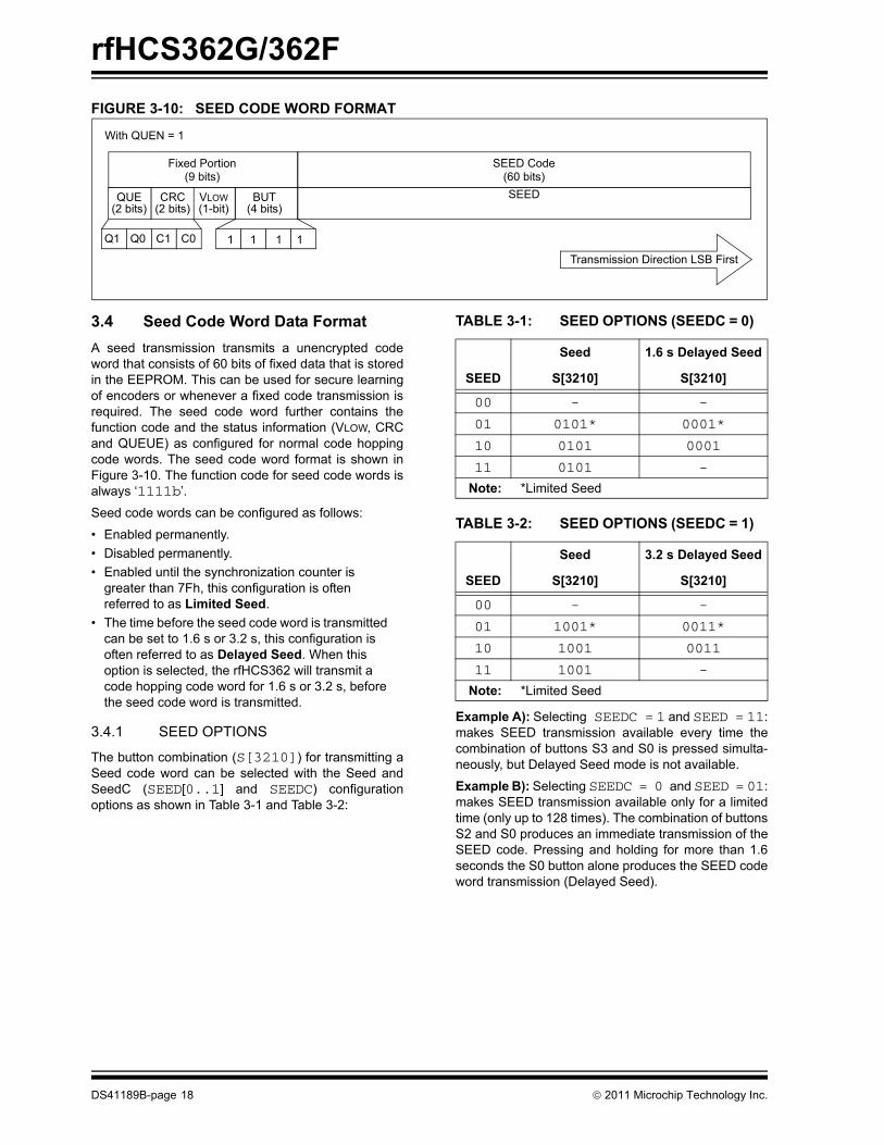
FIGURE 3-10: SEED CODE WORD FORMAT3.4 Seed Code Word Data FormatA seed transmission transmits a unencrypted codeword that consists of 60 bits of fixed data that is storedin the EEPROM. This can be used for secure learningof encoders or whenever a fixed code transmission isrequired. The seed code word further contains thefunction code and the status information (VLOW, CRCand QUEUE) as configured for normal code hoppingcode words. The seed code word format is shown inFigure 3-10. The function code for seed code words isalways ‘1111b’.
Seed code words can be configured as follows:
• Enabled permanently.• Disabled permanently.• Enabled until the synchronization counter is
greater than 7Fh, this configuration is often referred to as Limited Seed.
• The time before the seed code word is transmitted can be set to 1.6 s or 3.2 s, this configuration is often referred to as Delayed Seed. When this option is selected, the rfHCS362 will transmit a code hopping code word for 1.6 s or 3.2 s, before the seed code word is transmitted.
3.4.1 SEED OPTIONS
The button combination (S[3210]) for transmitting aSeed code word can be selected with the Seed andSeedC (SEED[0..1] and SEEDC) configurationoptions as shown in Table 3-1 and Table 3-2:
TABLE 3-1: SEED OPTIONS (SEEDC = 0)
TABLE 3-2: SEED OPTIONS (SEEDC = 1)
Example A): Selecting SEEDC = 1 and SEED = 11:makes SEED transmission available every time thecombination of buttons S3 and S0 is pressed simulta-neously, but Delayed Seed mode is not available.
Example B): Selecting SEEDC = 0 and SEED = 01:makes SEED transmission available only for a limitedtime (only up to 128 times). The combination of buttonsS2 and S0 produces an immediate transmission of theSEED code. Pressing and holding for more than 1.6seconds the S0 button alone produces the SEED codeword transmission (Delayed Seed).
Transmission Direction LSB First
Fixed Portion
QUE(2 bits)
CRC(2 bits)
VLOW(1-bit)
SEED
With QUEN = 1
BUT(4 bits)
(9 bits)SEED Code
(60 bits)
Q1 Q0 C1 C0 1 1 1 1
Seed 1.6 s Delayed Seed
SEED S[3210] S[3210]
00 - -
01 0101* 0001*
10 0101 0001
11 0101 -
Note: *Limited Seed
Seed 3.2 s Delayed Seed
SEED S[3210] S[3210]
00 - -
01 1001* 0011*
10 1001 0011
11 1001 -
Note: *Limited Seed
DS41189B-page 18 © 2011 Microchip Technology Inc.
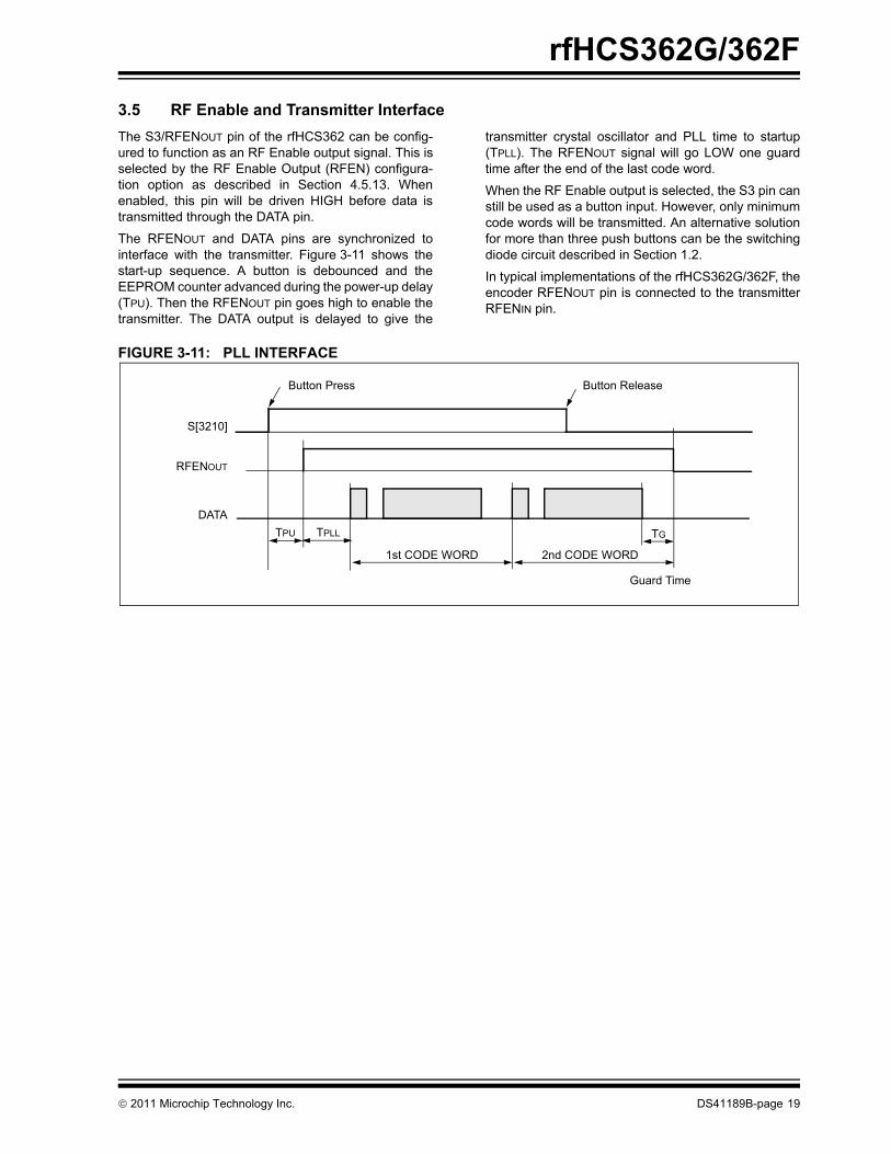
rfHCS362G/362F
3.5 RF Enable and Transmitter InterfaceThe S3/RFENOUT pin of the rfHCS362 can be config-ured to function as an RF Enable output signal. This isselected by the RF Enable Output (RFEN) configura-tion option as described in Section 4.5.13. Whenenabled, this pin will be driven HIGH before data istransmitted through the DATA pin.The RFENOUT and DATA pins are synchronized tointerface with the transmitter. Figure 3-11 shows thestart-up sequence. A button is debounced and theEEPROM counter advanced during the power-up delay(TPU). Then the RFENOUT pin goes high to enable thetransmitter. The DATA output is delayed to give the
transmitter crystal oscillator and PLL time to startup(TPLL). The RFENOUT signal will go LOW one guardtime after the end of the last code word.
When the RF Enable output is selected, the S3 pin canstill be used as a button input. However, only minimumcode words will be transmitted. An alternative solutionfor more than three push buttons can be the switchingdiode circuit described in Section 1.2.
In typical implementations of the rfHCS362G/362F, theencoder RFENOUT pin is connected to the transmitterRFENIN pin.
FIGURE 3-11: PLL INTERFACE
S[3210]
RFENOUT
DATATPLL
Guard Time
1st CODE WORD
TG
Button Press Button Release
2nd CODE WORD
TPU
© 2011 Microchip Technology Inc. DS41189B-page 19
rfHCS362G/362F
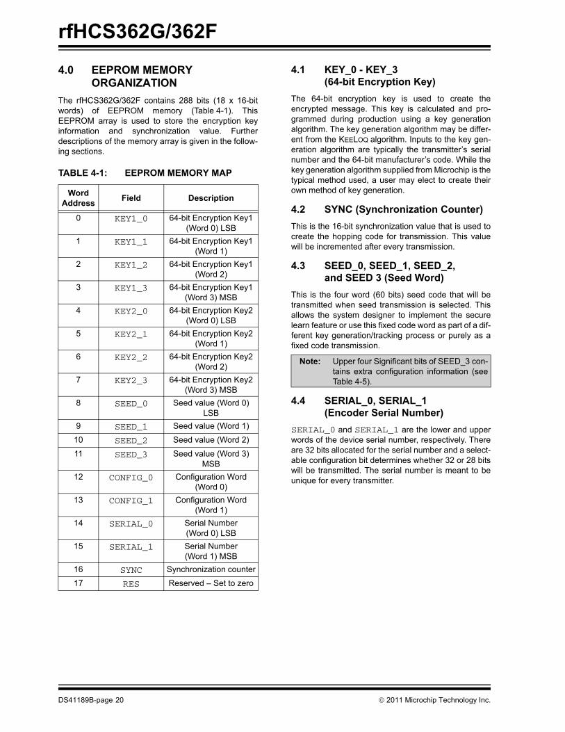
4.0 EEPROM MEMORY ORGANIZATION
The rfHCS362G/362F contains 288 bits (18 x 16-bitwords) of EEPROM memory (Table 4-1). ThisEEPROM array is used to store the encryption keyinformation and synchronization value. Furtherdescriptions of the memory array is given in the follow-ing sections.
TABLE 4-1: EEPROM MEMORY MAP
4.1 KEY_0 - KEY_3 (64-bit Encryption Key)
The 64-bit encryption key is used to create theencrypted message. This key is calculated and pro-grammed during production using a key generationalgorithm. The key generation algorithm may be differ-ent from the KEELOQ algorithm. Inputs to the key gen-eration algorithm are typically the transmitter’s serialnumber and the 64-bit manufacturer’s code. While thekey generation algorithm supplied from Microchip is thetypical method used, a user may elect to create theirown method of key generation.
4.2 SYNC (Synchronization Counter)This is the 16-bit synchronization value that is used tocreate the hopping code for transmission. This valuewill be incremented after every transmission.
4.3 SEED_0, SEED_1, SEED_2, and SEED 3 (Seed Word)
This is the four word (60 bits) seed code that will betransmitted when seed transmission is selected. Thisallows the system designer to implement the securelearn feature or use this fixed code word as part of a dif-ferent key generation/tracking process or purely as afixed code transmission.
4.4 SERIAL_0, SERIAL_1 (Encoder Serial Number)
SERIAL_0 and SERIAL_1 are the lower and upperwords of the device serial number, respectively. Thereare 32 bits allocated for the serial number and a select-able configuration bit determines whether 32 or 28 bitswill be transmitted. The serial number is meant to beunique for every transmitter.
Word Address Field Description
0 KEY1_0 64-bit Encryption Key1 (Word 0) LSB
1 KEY1_1 64-bit Encryption Key1 (Word 1)
2 KEY1_2 64-bit Encryption Key1 (Word 2)
3 KEY1_3 64-bit Encryption Key1 (Word 3) MSB
4 KEY2_0 64-bit Encryption Key2 (Word 0) LSB
5 KEY2_1 64-bit Encryption Key2 (Word 1)
6 KEY2_2 64-bit Encryption Key2 (Word 2)
7 KEY2_3 64-bit Encryption Key2 (Word 3) MSB
8 SEED_0 Seed value (Word 0) LSB
9 SEED_1 Seed value (Word 1)
10 SEED_2 Seed value (Word 2)
11 SEED_3 Seed value (Word 3) MSB
12 CONFIG_0 Configuration Word (Word 0)
13 CONFIG_1 Configuration Word (Word 1)
14 SERIAL_0 Serial Number (Word 0) LSB
15 SERIAL_1 Serial Number (Word 1) MSB
16 SYNC Synchronization counter
17 RES Reserved – Set to zero
Note: Upper four Significant bits of SEED_3 con-tains extra configuration information (seeTable 4-5).
DS41189B-page 20 © 2011 Microchip Technology Inc.
rfHCS362G/362F
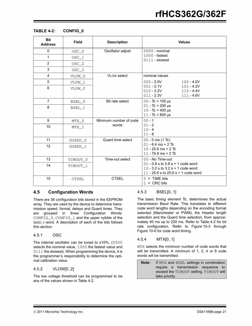
TABLE 4-2: CONFIG_04.5 Configuration WordsThere are 36 configuration bits stored in the EEPROMarray. They are used by the device to determine trans-mission speed, format, delays and Guard times. Theyare grouped in three Configuration Words:CONFIG_0, CONFIG_1 and the upper nybble of theSEED_3 word. A description of each of the bits followsthis section.
4.5.1 OSC
The internal oscillator can be tuned to ±10%. (0000selects the nominal value, 1000 the fastest value and0111 the slowest). When programming the device, it isthe programmer’s responsibility to determine the opti-mal calibration value.
4.5.2 VLOW[0..2]
The low voltage threshold can be programmed to beany of the values shown in Table 4-2.
4.5.3 BSEL[0..1]
The basic timing element TE, determines the actualtransmission Baud Rate. This translates to differentcode word lengths depending on the encoding formatselected (Manchester or PWM), the Header lengthselection and the Guard time selection, from approxi-mately 40 ms up to 220 ms. Refer to Table 4-2 for bitrate configuration. Refer to Figure 10-3 throughFigure 10-6 for code word timing.
4.5.4 MTX[0..1]
MTX selects the minimum number of code words thatwill be transmitted. A minimum of 1, 2, 4 or 8 codewords will be transmitted.
BitAddress Field Description Values
0 OSC_0 Oscillator adjust 0000 - nominal 1000 - fastest 0111 - slowest
1 OSC_1
2 OSC_2
3 OSC_3
4 VLOW_0 VLOW select nominal values
5 VLOW_1 000 - 2.0V001 - 2.1V010 - 2.2V011 - 2.3V
100 - 4.0V101 - 4.2V110 - 4.4V111 - 4.6V
6 VLOW_2
7 BSEL_0 Bit rate select 00 - TE = 100 μs01 - TE = 200 μs10 - TE = 400 μs11 - TE = 800 μs
8 BSEL_1
9 MTX_0 Minimum number of code words
00 - 101 - 210 - 411 - 8
10 MTX_1
11 GUARD_0 Guard time select 00 - 0 ms (1 TE)01 - 6.4 ms + 2 TE10 - 25.6 ms + 2 TE11 - 76.8 ms + 2 TE
12 GUARD_1
13 TIMOUT_0 Time-out select 00 - No Time-out01 - 0.8 s to 0.8 s + 1 code word10 - 3.2 s to 3.2 s + 1 code word11 - 25.6 s to 25.6 s + 1 code word
14 TIMOUT_1
15 CTSEL CTSEL 0 = TIME bits1 = CRC bits
Note: If MTX and BSEL settings in combinationrequire a transmission sequence toexceed the TIMOUT setting, TIMOUT willtake priority.
© 2011 Microchip Technology Inc. DS41189B-page 21
rfHCS362G/362F
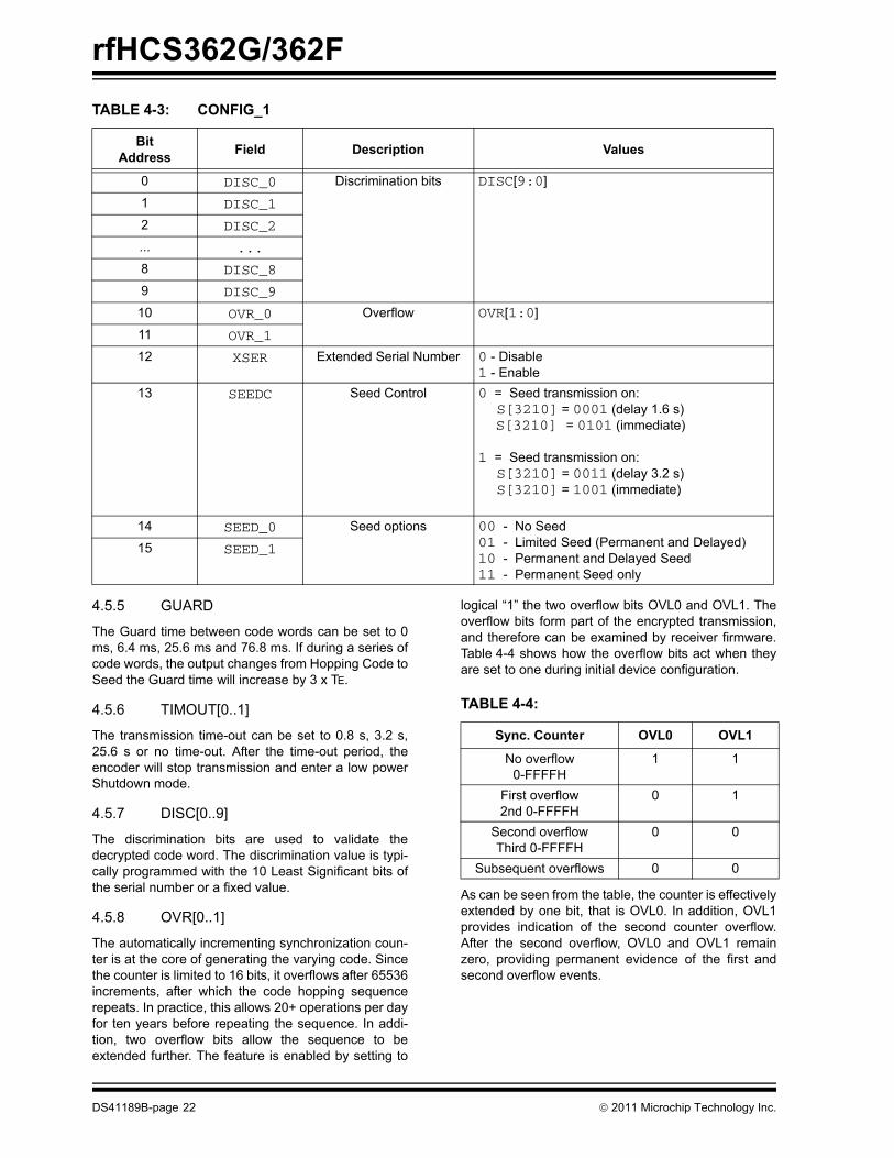
TABLE 4-3: CONFIG_14.5.5 GUARD
The Guard time between code words can be set to 0ms, 6.4 ms, 25.6 ms and 76.8 ms. If during a series ofcode words, the output changes from Hopping Code toSeed the Guard time will increase by 3 x TE.
4.5.6 TIMOUT[0..1]
The transmission time-out can be set to 0.8 s, 3.2 s,25.6 s or no time-out. After the time-out period, theencoder will stop transmission and enter a low powerShutdown mode.
4.5.7 DISC[0..9]
The discrimination bits are used to validate thedecrypted code word. The discrimination value is typi-cally programmed with the 10 Least Significant bits ofthe serial number or a fixed value.
4.5.8 OVR[0..1]
The automatically incrementing synchronization coun-ter is at the core of generating the varying code. Sincethe counter is limited to 16 bits, it overflows after 65536increments, after which the code hopping sequencerepeats. In practice, this allows 20+ operations per dayfor ten years before repeating the sequence. In addi-tion, two overflow bits allow the sequence to beextended further. The feature is enabled by setting to
logical “1” the two overflow bits OVL0 and OVL1. Theoverflow bits form part of the encrypted transmission,and therefore can be examined by receiver firmware.Table 4-4 shows how the overflow bits act when theyare set to one during initial device configuration.
TABLE 4-4:
As can be seen from the table, the counter is effectivelyextended by one bit, that is OVL0. In addition, OVL1provides indication of the second counter overflow.After the second overflow, OVL0 and OVL1 remainzero, providing permanent evidence of the first andsecond overflow events.
BitAddress Field Description Values
0 DISC_0 Discrimination bits DISC[9:0]
1 DISC_1
2 DISC_2
... ...
8 DISC_8
9 DISC_9
10 OVR_0 Overflow OVR[1:0]
11 OVR_1
12 XSER Extended Serial Number 0 - Disable1 - Enable
13 SEEDC Seed Control 0 = Seed transmission on: S[3210] = 0001 (delay 1.6 s) S[3210] = 0101 (immediate)
1 = Seed transmission on: S[3210] = 0011 (delay 3.2 s) S[3210] = 1001 (immediate)
14 SEED_0 Seed options 00 - No Seed01 - Limited Seed (Permanent and Delayed)10 - Permanent and Delayed Seed11 - Permanent Seed only
15 SEED_1
Sync. Counter OVL0 OVL1
No overflow 0-FFFFH
1 1
First overflow 2nd 0-FFFFH
0 1
Second overflow Third 0-FFFFH
0 0
Subsequent overflows 0 0
DS41189B-page 22 © 2011 Microchip Technology Inc.
rfHCS362G/362F
4.5.9 XSERIf XSER is enabled a 32-bit serial number is transmit-ted. If XSER is disabled a 28-bit serial number and a4-bit function code are transmitted.
4.5.10 SEED[0..1]
The seed value which is transmitted on key combina-tions (0011) and (1001) can be disabled, enabled orenabled for a limited number of transmissions deter-mined by the initial counter value.
In limited Seed mode, the device will output the seed ifthe sync counter (Section 4.2) is from 00hex to 7Fhex.For a counter higher than 7F, a normal hopping codewill be output.
4.5.11 SEEDC
SEEDC selects between seed transmission on 0001and 0101 (SEEDC = 0) and 0011 and 1001 (SEEDC= 1). The delay before seed transmission is 1.6 s for(SEEDC = 0) and 3.2 s for (SEEDC = 1).
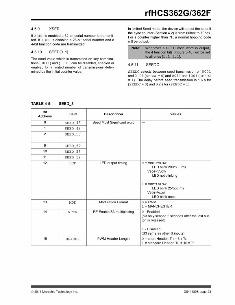
TABLE 4-5: SEED_3
Note: Whenever a SEED code word is output,the 4 function bits (Figure 3-10) will be setto all ones [1,1,1,1].
BitAddress Field Description Values
0 SEED_48 Seed Most Significant word —
1 SEED_49
2 SEED_50
... ...
9 SEED_57
10 SEED_58
11 SEED_59
12 LED LED output timing 0 = VBOT>VLOW LED blink 200/800 ms VBOT<VLOW LED not blinking
1 = VBOT>VLOW LED blink 25/500 ms VBOT<VLOW LED blink once
13 MOD Modulation Format 0 = PWM1 = MANCHESTER
14 RFEN RF Enable/S3 multiplexing 0 - Enabled (S3 only sensed 2 seconds after the last but-ton is released)
1 - Disabled (S3 same as other S inputs)
15 HEADER PWM Header Length 0 = short Header, TH = 3 x TE1 = standard Header, TH = 10 x TE
© 2011 Microchip Technology Inc. DS41189B-page 23
rfHCS362G/362F
4.5.12 HEADERWhen PWM mode is selected the header length (lowtime between preamble and data bits start) can be setto 10 x TE or 3 x TE. The 10 x TE mode is recommendedfor compatibility with previous KEELOQ encoder mod-els. In Manchester mode, the header length is fixed andset to 4 x TE.
4.5.13 RFEN
RFEN selects whether the RFEN output is enabled ordisabled. If enabled, S3 is only sampled 2 s after thelast button is released and at the start of the first trans-
mission. If disabled S3 functions the same as the otherS inputs. For typical implementation of the rfHCS362G/362F the RFEN bit = 0.
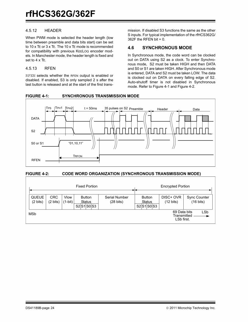
4.6 SYNCHRONOUS MODEIn Synchronous mode, the code word can be clockedout on DATA using S2 as a clock. To enter Synchro-nous mode, S2 must be taken HIGH and then DATAand S0 or S1 are taken HIGH. After Synchronous modeis entered, DATA and S2 must be taken LOW. The datais clocked out on DATA on every falling edge of S2.Auto-shutoff timer is not disabled in Synchronousmode. Refer to Figure 4-1 and Figure 4-2.
FIGURE 4-1: SYNCHRONOUS TRANSMISSION MODE
FIGURE 4-2: CODE WORD ORGANIZATION (SYNCHRONOUS TRANSMISSION MODE)
“01,10,11”
DATA
S2
S0 or S1
TPS TPH1 TPH2 t = 50ms Preamble Header Data
RFENTRFON
35 pulses on S2
QUEUE(2 bits)
CRC(2 bits)
Vlow(1-bit)
Button Status
S2 S1 S0 S3
Serial Number(28 bits)
Button Status
S2 S1 S0 S3
DISC+ OVR(12 bits)
Sync Counter(16 bits)
69 Data bitsTransmitted
LSb first.
LSbMSb
Fixed Portion Encrypted Portion
DS41189B-page 24 © 2011 Microchip Technology Inc.
rfHCS362G/362F
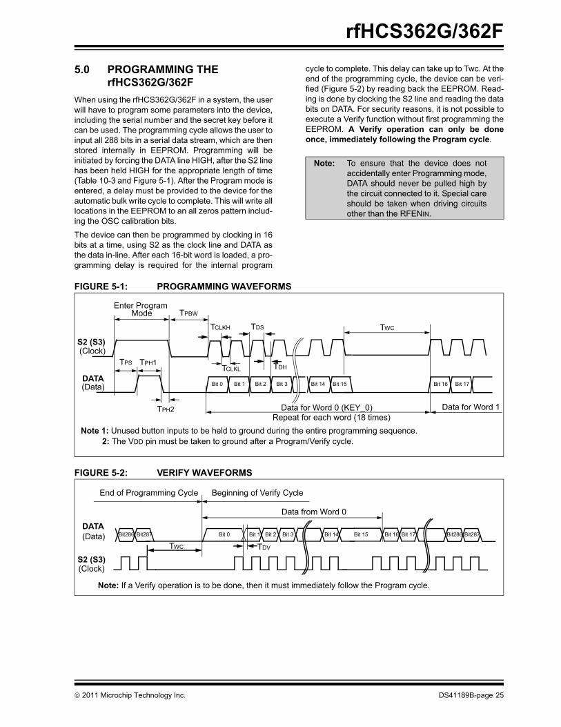
5.0 PROGRAMMING THE rfHCS362G/362F
When using the rfHCS362G/362F in a system, the userwill have to program some parameters into the device,including the serial number and the secret key before itcan be used. The programming cycle allows the user toinput all 288 bits in a serial data stream, which are thenstored internally in EEPROM. Programming will beinitiated by forcing the DATA line HIGH, after the S2 linehas been held HIGH for the appropriate length of time(Table 10-3 and Figure 5-1). After the Program mode isentered, a delay must be provided to the device for theautomatic bulk write cycle to complete. This will write alllocations in the EEPROM to an all zeros pattern includ-ing the OSC calibration bits.
The device can then be programmed by clocking in 16bits at a time, using S2 as the clock line and DATA asthe data in-line. After each 16-bit word is loaded, a pro-gramming delay is required for the internal program
cycle to complete. This delay can take up to Twc. At theend of the programming cycle, the device can be veri-fied (Figure 5-2) by reading back the EEPROM. Read-ing is done by clocking the S2 line and reading the databits on DATA. For security reasons, it is not possible toexecute a Verify function without first programming theEEPROM. A Verify operation can only be doneonce, immediately following the Program cycle.
FIGURE 5-1: PROGRAMMING WAVEFORMS
FIGURE 5-2: VERIFY WAVEFORMS
Note: To ensure that the device does notaccidentally enter Programming mode,DATA should never be pulled high bythe circuit connected to it. Special careshould be taken when driving circuitsother than the RFENIN.
DATA
Enter Program Mode
(Data)
(Clock)
Note 1: Unused button inputs to be held to ground during the entire programming sequence.
Bit 0 Bit 1 Bit 2 Bit 3 Bit 14 Bit 15 Bit 16 Bit 17
TPH1
TPBW
TPS
Repeat for each word (18 times)TPH2
TCLKH
TCLKL
TWCTDS
S2 (S3)
Data for Word 0 (KEY_0) Data for Word 1
TDH
2: The VDD pin must be taken to ground after a Program/Verify cycle.
DATA
(Clock)
(Data)
Note: If a Verify operation is to be done, then it must immediately follow the Program cycle.
End of Programming Cycle Beginning of Verify Cycle
Bit 1 Bit 2 Bit 3 Bit 15Bit 14 Bit 16 Bit 17 Bit286 Bit287
TWC
Data from Word 0
TDV
S2 (S3)
Bit 0Bit287Bit286
© 2011 Microchip Technology Inc. DS41189B-page 25
rfHCS362G/362F
6.0 UHF ASK/FSK TRANSMITTER
6.1 Transmitter OperationThe transmitter is a fully integrated UHF ASK/FSKtransmitter consisting of crystal oscillator, Phase-Locked Loop (PLL), open-collector differential-outputPower Amplifier (PA), and mode control logic. Externalcomponents consist of bypass capacitors, crystal, andPLL loop filter. The rfHCS362G is capable of AmplitudeShift Keying (ASK) modulation. The rfHCS362F iscapable of ASK or Frequency Shift Keying (FSK) mod-ulation by employing an internal FSK switch to pull thetransmitter crystal via a second load capacitor.
Figure 2-1 shows the internal structure of the transmit-ter. Transmitter connections are independent from theencoder to provide for maximum design flexibility.Example application circuits for ASK or FSK modula-tion are presented in Section 1.2.
The rfHCS362G/362F are radio frequency (RF) emit-ting devices. Wireless RF devices are governed by acountry’s regulating agency. For example, in the UnitedStates it is the Federal Communications Committee(FCC) and in Europe it is the European Conference ofPostal and Telecommunications Administrations(CEPT). It is the responsibility of the designer to ensurethat their end product conforms to rules and regulationsof the country of use and/or sale.
6.2 Supply Voltage (VDDRF, VSSRF)Pins VDDRF and VSSRF supply power and groundrespectively to the transmitter. These power pins areseparate from power supply pins VDD and VSS to theencoder.
6.3 Crystal OscillatorThe transmitter crystal oscillator is a Colpitts oscillatorthat provides the reference frequency to the PLL. It isindependent from the encoder oscillator. An externalcrystal or AC coupled reference signal is connected tothe XTAL pin. The transmit frequency is fixed anddetermined by the crystal frequency according to theformula:
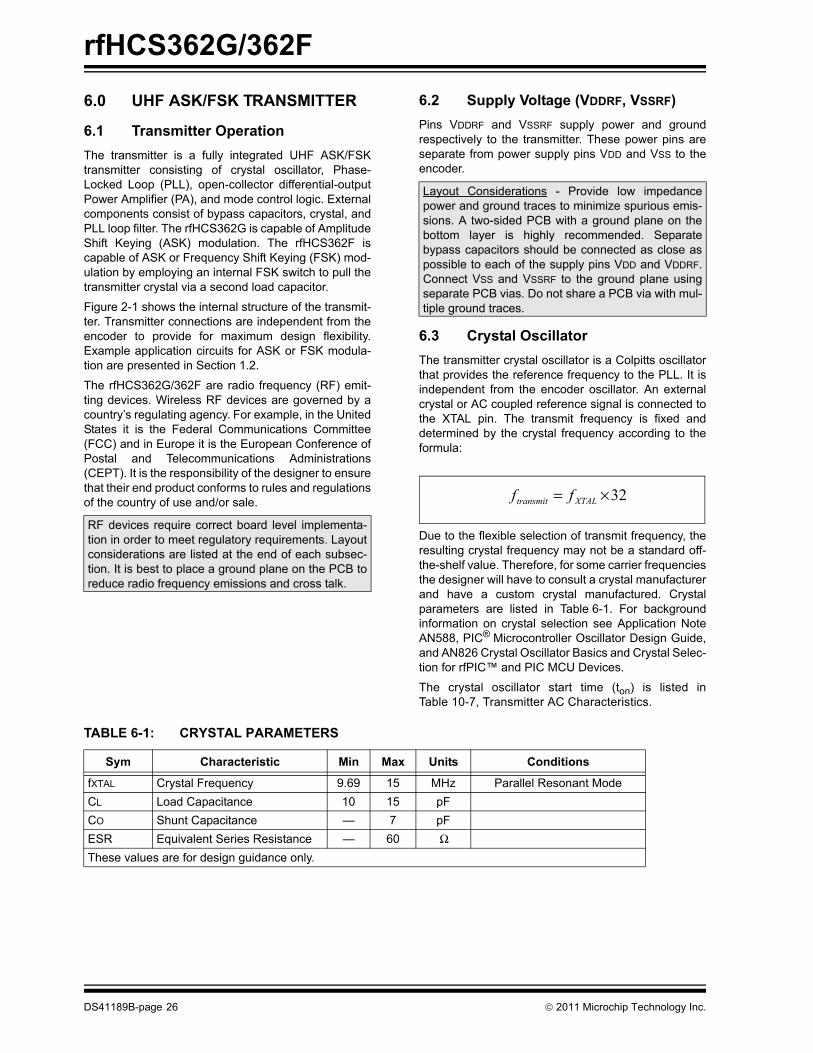
Due to the flexible selection of transmit frequency, theresulting crystal frequency may not be a standard off-the-shelf value. Therefore, for some carrier frequenciesthe designer will have to consult a crystal manufacturerand have a custom crystal manufactured. Crystalparameters are listed in Table 6-1. For backgroundinformation on crystal selection see Application NoteAN588, PIC® Microcontroller Oscillator Design Guide,and AN826 Crystal Oscillator Basics and Crystal Selec-tion for rfPIC™ and PIC MCU Devices.
The crystal oscillator start time (ton) is listed inTable 10-7, Transmitter AC Characteristics.
TABLE 6-1: CRYSTAL PARAMETERS
RF devices require correct board level implementa-tion in order to meet regulatory requirements. Layoutconsiderations are listed at the end of each subsec-tion. It is best to place a ground plane on the PCB toreduce radio frequency emissions and cross talk.
Layout Considerations - Provide low impedancepower and ground traces to minimize spurious emis-sions. A two-sided PCB with a ground plane on thebottom layer is highly recommended. Separatebypass capacitors should be connected as close aspossible to each of the supply pins VDD and VDDRF.Connect VSS and VSSRF to the ground plane usingseparate PCB vias. Do not share a PCB via with mul-tiple ground traces.
32×= XTALtransmit ff
Sym Characteristic Min Max Units Conditions
fXTAL Crystal Frequency 9.69 15 MHz Parallel Resonant ModeCL Load Capacitance 10 15 pFCO Shunt Capacitance — 7 pFESR Equivalent Series Resistance — 60 ΩThese values are for design guidance only.
DS41189B-page 26 © 2011 Microchip Technology Inc.
rfHCS362G/362F
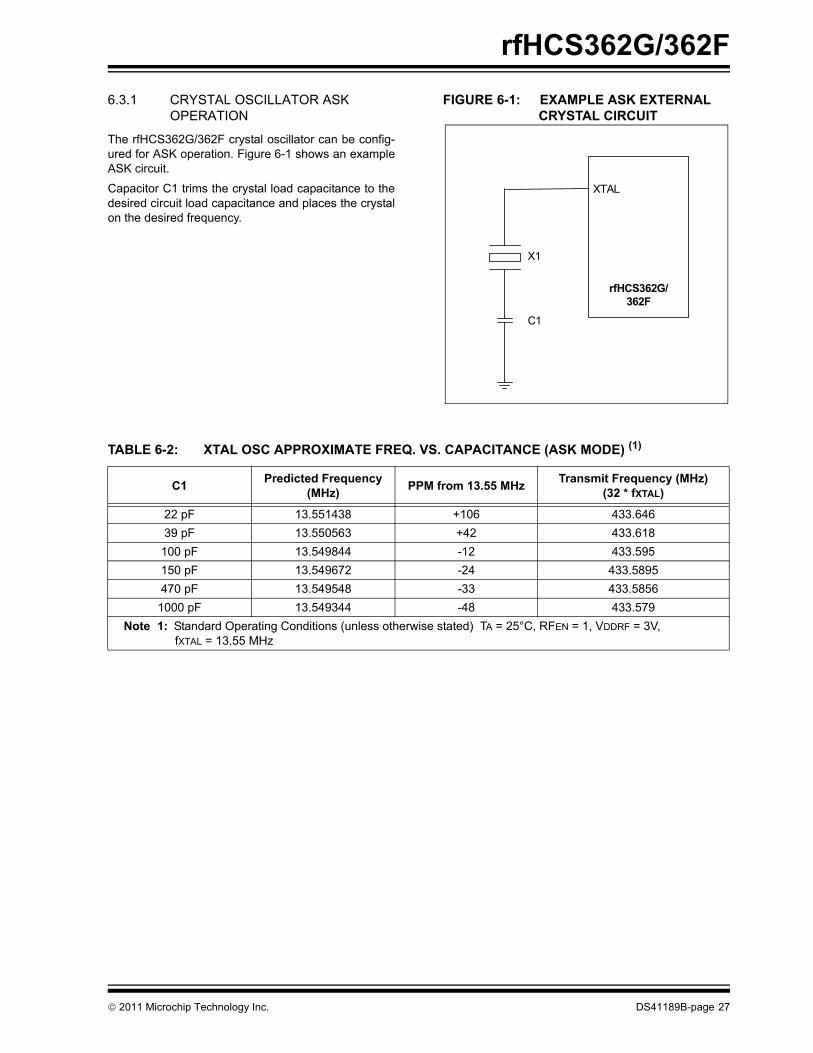
6.3.1 CRYSTAL OSCILLATOR ASKOPERATION
The rfHCS362G/362F crystal oscillator can be config-ured for ASK operation. Figure 6-1 shows an exampleASK circuit.
Capacitor C1 trims the crystal load capacitance to thedesired circuit load capacitance and places the crystalon the desired frequency.
FIGURE 6-1: EXAMPLE ASK EXTERNAL CRYSTAL CIRCUIT
TABLE 6-2: XTAL OSC APPROXIMATE FREQ. VS. CAPACITANCE (ASK MODE) (1)
XTAL
rfHCS362G/362F
X1
C1
C1 Predicted Frequency (MHz) PPM from 13.55 MHz Transmit Frequency (MHz)
(32 * fXTAL)
22 pF 13.551438 +106 433.64639 pF 13.550563 +42 433.618100 pF 13.549844 -12 433.595150 pF 13.549672 -24 433.5895470 pF 13.549548 -33 433.5856
1000 pF 13.549344 -48 433.579Note 1: Standard Operating Conditions (unless otherwise stated) TA = 25°C, RFEN = 1, VDDRF = 3V,
fXTAL = 13.55 MHz
© 2011 Microchip Technology Inc. DS41189B-page 27
rfHCS362G/362F
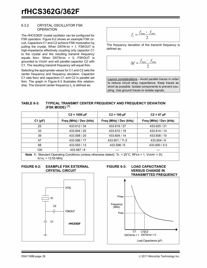
6.3.2 CRYSTAL OSCILLATOR FSKOPERATION
The rfHCS362F crystal oscillator can be configured forFSK operation. Figure 6-2 shows an example FSK cir-cuit. Capacitors C1 and C2 achieve FSK modulation bypulling the crystal. When DATAFSK = 1, FSKOUT ishigh-impedance effectively coupling only capacitor C1to the crystal and the resulting transmit frequencyequals fMAX. When DATAFSK = 0, FSKOUT isgrounded to VSSRF and will parallel capacitor C2 withC1. The resulting transmit frequency will equal fMIN.
Selecting the appropriate values for C1 and C2 sets thecenter frequency and frequency deviation. CapacitorC1 sets fMAX and capacitors C1 and C2 in parallel setfMIN. The graph in Figure 6-3 illustrates this relation-ship. The transmit center frequency fC is defined as:
The frequency deviation of the transmit frequency isdefined as:
TABLE 6-3: TYPICAL TRANSMIT CENTER FREQUENCY AND FREQUENCY DEVIATION (FSK MODE) (1)
FIGURE 6-2: EXAMPLE FSK EXTERNAL CRYSTAL CIRCUIT
FIGURE 6-3: LOAD CAPACITANCE VERSUS CHANGE IN TRANSMITTED FREQUENCY
Layout considerations - Avoid parallel traces in orderto reduce circuit stray capacitance. Keep traces asshort as possible. Isolate components to prevent cou-pling. Use ground traces to isolate signals.
2minmax fffc
+=
2minmax fff −=Δ
C2 = 1000 pF C2 = 100 pF C2 = 47 pF
C1 (pF) Freq (MHz) / Dev (kHz) Freq (MHz) / Dev (kHz) Freq (MHz) / Dev (kHz)
22 433.612 / 34 433.619 / 27 433.625 / 2133 433.604 / 25 433.610 / 19 433.614 / 1439 433.598 / 20 433.604 / 14 433.608 / 1047 433.596 / 17 433.601 / 11.5 433.604 / 868 433.593 / 13 433.598 / 9 433.600 / 5.5
100 433.587 / 8 — —Note 1: Standard Operating Conditions (unless otherwise stated) TA = 25°C, RFEN = 1, VDDRF = 3V,
fXTAL = 13.55 MHz
XTAL
rfHCS362F
X1
C1
C2
FSKOUT
Frequency(MHz)
Fmax
Fmin
C1 C1||C2DATAFSK = 1 DATAFSK = 0
Load Capacitance (pF)
DS41189B-page 28 © 2011 Microchip Technology Inc.
rfHCS362G/362F
6.4 Clock Output (CLKOUT)The crystal oscillator feeds a divide-by-four circuit thatprovides a clock output at the CLKOUT pin. CLKOUTis slew-rate limited in order to keep spurious signalemissions as low as possible. The voltage swing(VCLKOUT) depends on the capacitive loading (CLOAD)on the CLKOUT pin (2 VPP at 5 pF).6.5 Phase-Locked Loop (PLL)The PLL consists of a Phase-frequency Detector(PFD), charge pump, Voltage-controlled Oscillator(VCO), and fixed divide-by-32 divider. An external loopfilter is connected to pin LF. The loop filter controls thedynamic behavior of the PLL, primarily lock time andspur levels. The application determines the loop filterrequirements.
The rfHCS362 employs a charge pump PLL that offersmany advantages over the classical voltage phasedetector PLL: infinite pull-in range and zero steadystate phase error. The charge pump PLL allows the useof passive loop filters that are lower cost and minimizenoise. Charge pump PLLs have reduced flicker noisethus limiting phase noise. Many of the classical texts onPLLs do not cover this type of PLL, however, today thisis the most common type of PLL. This data sheet brieflycovers the general terms and design requirements forthe rfPIC. Detailed PLL design and operation is beyondthe scope of this data sheet. For more information, thedesigner is referred to "PLL Performance, Simulation,and Design," Second Edition by Dean Banerjee ISBN0970820704. Banerjee covers charge pump PLLs andloop filter selection.
The loop filter has a major impact on lock time and spurlevels. Lock time is the time it takes the PLL to lock onfrequency. When the PLL is first powered on or ischanging frequencies, no data can be transmitted.Lock time must be considered before data transmissioncan begin. In addition to PLL lock time, the designermust take into account the crystal oscillator start time ofapproximately 1 ms. See Section 6.3 for more informa-tion about the crystal oscillator. Reference spurs occurat the carrier frequency plus and minus integer multi-ples of the reference frequency. Phase noise refers tonoise generated by the PLL. Spur levels and phasenoise can increase the signal to noise ratio (SNR) ofthe system and mask or degrade the transmitted sig-nal.
The first order effect on PLL performance is loop band-width. Loop bandwidth (ωc) is defined as the pointwhere the open loop phase transfer function equals 0dB. Selecting a small loop bandwidth results in lowerspur levels but slower lock time. Selecting a larger loopbandwidth results in a faster lock time but higher spurlevels.
Second order effects on PLL performance is Phasemargin (φ) and Damping factor (ζ). Phase margin is ameasure of PLL stability. Choosing a phase margin thatis too low will result in PLL instability. Choosing a higherphase margin results in less ringing and faster lock timeat the expense of higher spur levels. Loop filters aretypically designed for a total phase margin between 30and 70 degrees. The aim of the designer is to choosea loop bandwidth and phase margin that gives the fast-est possible lock time and meets the spur level require-ments of the application.
Damping factor governs the second order transientresponse that determines the shape of the exponentialenvelope of the natural frequency. The natural fre-quency, also called ringing frequency, is the frequencyof the VCO steering voltage as the PLL settles. Locktime is proportional to damping factor and inverselyproportional to loop bandwidth.
The application determines the loop filter componentrequirements. For example, if the transmit frequencyselected is near band edges or restricted bands, spurlevels must be reduced to meet regulatory require-ments. However, this will be at the expense of locktime. For an FSK application, a larger damping factor(≅ 1.0) is desired so that there is less overshoot in thekeying of FSK. For an ASK application, a damping fac-tor = 0.707 results in less settling time and near opti-mum noise performance.
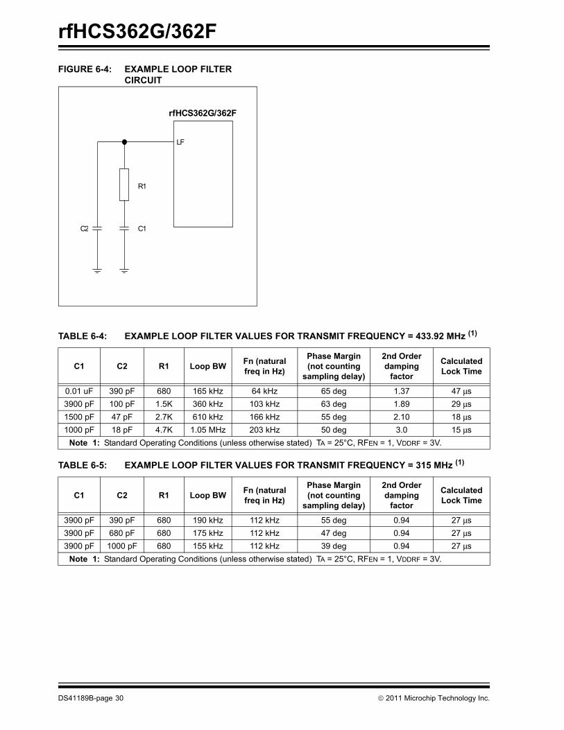
Figure 6-4 shows an example passive second orderloop filter circuit. Table 6-4 gives example loop filter val-ues for a crystal frequency of 13.56 MHz and transmitfrequency of 433.92 MHz. Table 6-5 gives exampleloop filter values for a crystal frequency of 9.84375MHz and transmit frequency of 315 MHz.
Layout considerations - Shield each side of the clockoutput trace with ground traces to isolate the CLK-OUT signal and reduce coupling.
Layout considerations - Keep traces short and placeloop filter components as close as possible to the LFpin.
© 2011 Microchip Technology Inc. DS41189B-page 29
rfHCS362G/362F
FIGURE 6-4: EXAMPLE LOOP FILTERCIRCUIT
TABLE 6-4: EXAMPLE LOOP FILTER VALUES FOR TRANSMIT FREQUENCY = 433.92 MHz (1)
TABLE 6-5: EXAMPLE LOOP FILTER VALUES FOR TRANSMIT FREQUENCY = 315 MHz (1)
LF
rfHCS362G/362F
R1
C1C2
C1 C2 R1 Loop BW Fn (natural freq in Hz)
Phase Margin (not counting
sampling delay)
2nd Order damping
factor
Calculated Lock Time
0.01 uF 390 pF 680 165 kHz 64 kHz 65 deg 1.37 47 μs3900 pF 100 pF 1.5K 360 kHz 103 kHz 63 deg 1.89 29 μs1500 pF 47 pF 2.7K 610 kHz 166 kHz 55 deg 2.10 18 μs1000 pF 18 pF 4.7K 1.05 MHz 203 kHz 50 deg 3.0 15 μs
Note 1: Standard Operating Conditions (unless otherwise stated) TA = 25°C, RFEN = 1, VDDRF = 3V.
C1 C2 R1 Loop BW Fn (natural freq in Hz)
Phase Margin (not counting
sampling delay)
2nd Order damping
factor
Calculated Lock Time
3900 pF 390 pF 680 190 kHz 112 kHz 55 deg 0.94 27 μs3900 pF 680 pF 680 175 kHz 112 kHz 47 deg 0.94 27 μs3900 pF 1000 pF 680 155 kHz 112 kHz 39 deg 0.94 27 μs
Note 1: Standard Operating Conditions (unless otherwise stated) TA = 25°C, RFEN = 1, VDDRF = 3V.
DS41189B-page 30 © 2011 Microchip Technology Inc.
rfHCS362G/362F
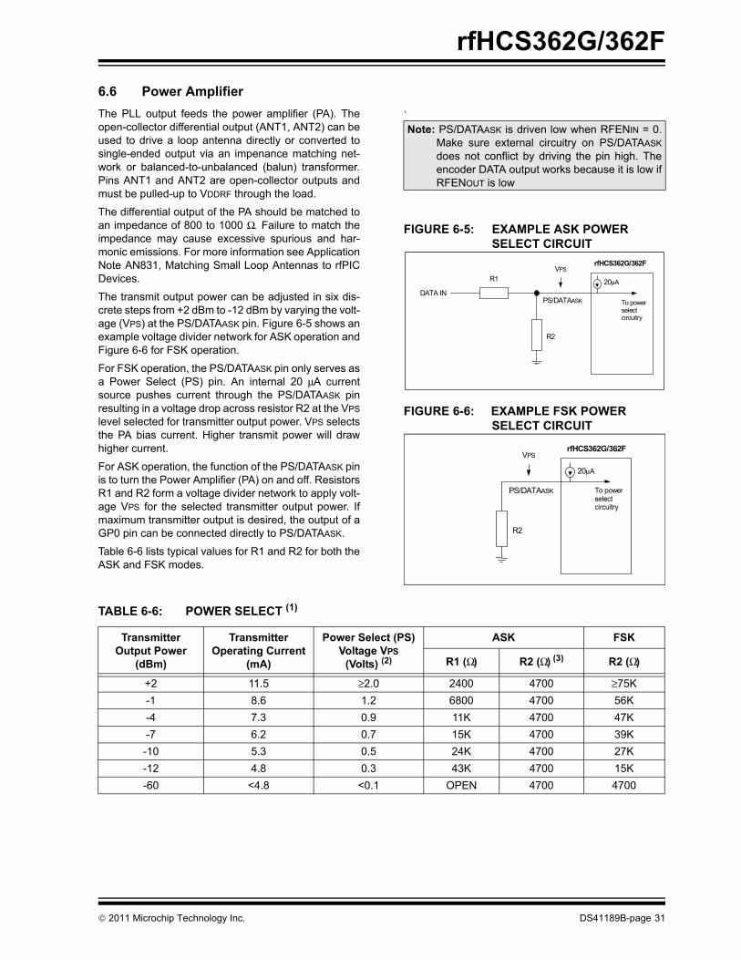
6.6 Power AmplifierThe PLL output feeds the power amplifier (PA). Theopen-collector differential output (ANT1, ANT2) can beused to drive a loop antenna directly or converted tosingle-ended output via an impenance matching net-work or balanced-to-unbalanced (balun) transformer.Pins ANT1 and ANT2 are open-collector outputs andmust be pulled-up to VDDRF through the load.The differential output of the PA should be matched toan impedance of 800 to 1000 Ω. Failure to match theimpedance may cause excessive spurious and har-monic emissions. For more information see ApplicationNote AN831, Matching Small Loop Antennas to rfPICDevices.
The transmit output power can be adjusted in six dis-crete steps from +2 dBm to -12 dBm by varying the volt-age (VPS) at the PS/DATAASK pin. Figure 6-5 shows anexample voltage divider network for ASK operation andFigure 6-6 for FSK operation.
For FSK operation, the PS/DATAASK pin only serves asa Power Select (PS) pin. An internal 20 μA currentsource pushes current through the PS/DATAASK pinresulting in a voltage drop across resistor R2 at the VPSlevel selected for transmitter output power. VPS selectsthe PA bias current. Higher transmit power will drawhigher current.
For ASK operation, the function of the PS/DATAASK pinis to turn the Power Amplifier (PA) on and off. ResistorsR1 and R2 form a voltage divider network to apply volt-age VPS for the selected transmitter output power. Ifmaximum transmitter output is desired, the output of aGP0 pin can be connected directly to PS/DATAASK.
Table 6-6 lists typical values for R1 and R2 for both theASK and FSK modes.
.
FIGURE 6-5: EXAMPLE ASK POWER SELECT CIRCUIT
FIGURE 6-6: EXAMPLE FSK POWER SELECT CIRCUIT
TABLE 6-6: POWER SELECT (1)
Note: PS/DATAASK is driven low when RFENIN = 0.Make sure external circuitry on PS/DATAASKdoes not conflict by driving the pin high. Theencoder DATA output works because it is low ifRFENOUT is low
PS/DATAASK
rfHCS362G/362F
R2
R1
DATA IN
VPS
20μA
To powerselectcircuitry
PS/DATAASK
rfHCS362G/362F
R2
VPS
20μA
To powerselectcircuitry
Transmitter Output Power
(dBm)
Transmitter Operating Current
(mA)
Power Select (PS) Voltage VPS
(Volts) (2)
ASK FSK
R1 (Ω) R2 (Ω) (3) R2 (Ω)
+2 11.5 ≥2.0 2400 4700 ≥75K-1 8.6 1.2 6800 4700 56K-4 7.3 0.9 11K 4700 47K-7 6.2 0.7 15K 4700 39K-10 5.3 0.5 24K 4700 27K-12 4.8 0.3 43K 4700 15K-60 <4.8 <0.1 OPEN 4700 4700
© 2011 Microchip Technology Inc. DS41189B-page 31
rfHCS362G/362F
Note 1: Standard Operating Conditions (unless otherwise stated) TA = 25°C, RFEN = 1, VDDRF = 3V, fTRANSMIT = 433.92 MHz
2: VPS is actual voltage on PS/DATAASK pin.
3: The Power Select circuitry contains an internal 20 μA current source. To ensure that the transmitter outputpower is at the minimum when transmitting a DATAASK = 0 (VSSRF), select the value of resistor R2 suchthat the voltage drop across it is less than 0.1 volts.
DS41189B-page 32 © 2011 Microchip Technology Inc.
rfHCS362G/362F
6.7 Mode Control LogicThe mode control logic pin RFENIN controls the oper-ation of the transmitter (Table 6-7). When RFENINgoes high, the crystal oscillator starts up. The voltageon the LF pin ramps up proportionally to the RF fre-quency. The PLL can lock onto the frequency fasterthan the starting up crystal can stabilize. When the LFpin reaches 0.8V, the RF frequency is close to lockedon the crystal frequency. This initiates a 150 micro-second delay to ensure that the PLL settles. After thedelay, the PS/DATAASK bias current and power ampli-fier are enabled to start transmitting.When RFENIN goes low, the transmitter goes into lowpower Standby mode. The power amplifier is dis-abled, the crystal oscillator stops, and the PS/DATA-ASK pin is driven low. This will be a conflict if othercircuitry drives the PS/DATAASK pin high while RFENINis low. The encoder DATA pin is typically the only con-nection to PS/DATAASK and it always drives DATA lowbefore RFENOUT goes low.
For most applications the RFENIN pin is connecteddirectly to the RFENOUT pin. The RFENIN pin has aninternal pull-down resistor.
TABLE 6-7: RFENIN PIN STATES
RFEN Description
0 Transmitter and CLKOUT in Standby1 Transmitter and CLKOUT enabled
© 2011 Microchip Technology Inc. DS41189B-page 33
rfHCS362G/362F
7.0 INTEGRATING THE rfHCS362G/362F INTO THE SYSTEM
Use of the rfHCS362G/362F in a system requires acompatible decoder. This decoder is typically a micro-controller with compatible firmware. Microchip will pro-vide (via a license agreement) firmware routines thataccept transmissions from the rfHCS362G/362F anddecrypt the hopping code portion of the data stream.These routines provide system designers the means todevelop their own decoding system.
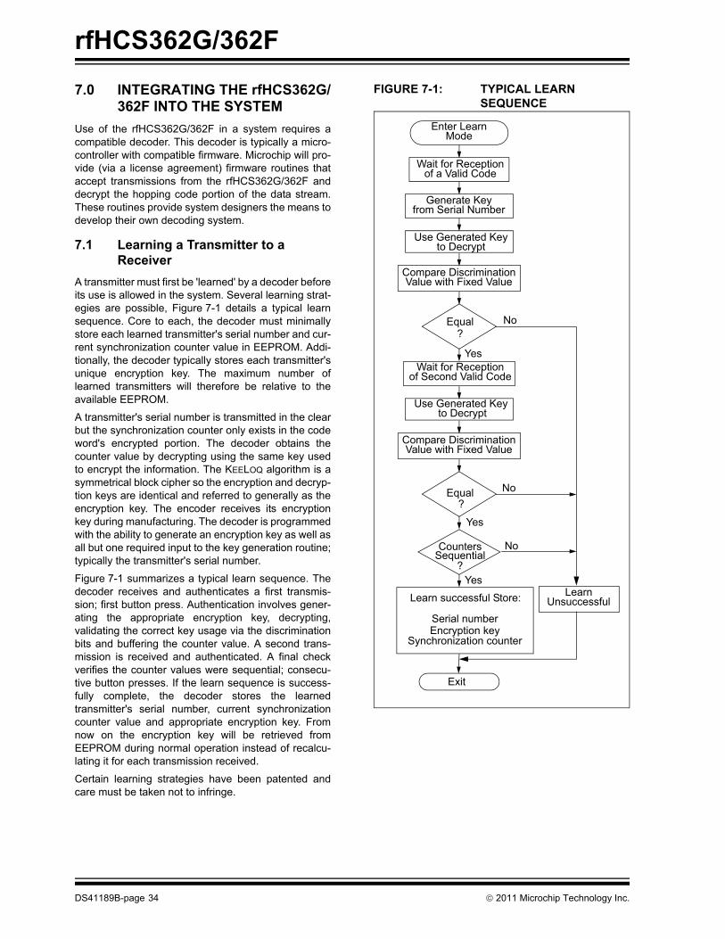
7.1 Learning a Transmitter to a Receiver
A transmitter must first be 'learned' by a decoder beforeits use is allowed in the system. Several learning strat-egies are possible, Figure 7-1 details a typical learnsequence. Core to each, the decoder must minimallystore each learned transmitter's serial number and cur-rent synchronization counter value in EEPROM. Addi-tionally, the decoder typically stores each transmitter'sunique encryption key. The maximum number oflearned transmitters will therefore be relative to theavailable EEPROM.
A transmitter's serial number is transmitted in the clearbut the synchronization counter only exists in the codeword's encrypted portion. The decoder obtains thecounter value by decrypting using the same key usedto encrypt the information. The KEELOQ algorithm is asymmetrical block cipher so the encryption and decryp-tion keys are identical and referred to generally as theencryption key. The encoder receives its encryptionkey during manufacturing. The decoder is programmedwith the ability to generate an encryption key as well asall but one required input to the key generation routine;typically the transmitter's serial number.
Figure 7-1 summarizes a typical learn sequence. Thedecoder receives and authenticates a first transmis-sion; first button press. Authentication involves gener-ating the appropriate encryption key, decrypting,validating the correct key usage via the discriminationbits and buffering the counter value. A second trans-mission is received and authenticated. A final checkverifies the counter values were sequential; consecu-tive button presses. If the learn sequence is success-fully complete, the decoder stores the learnedtransmitter's serial number, current synchronizationcounter value and appropriate encryption key. Fromnow on the encryption key will be retrieved fromEEPROM during normal operation instead of recalcu-lating it for each transmission received.
Certain learning strategies have been patented andcare must be taken not to infringe.
FIGURE 7-1: TYPICAL LEARN SEQUENCE
Enter LearnMode
Wait for Receptionof a Valid Code
Generate Keyfrom Serial Number
Use Generated Keyto Decrypt
Compare DiscriminationValue with Fixed Value
Equal
Wait for Receptionof Second Valid Code
Compare DiscriminationValue with Fixed Value
Use Generated Key to Decrypt
Equal
Counters
Encryption keySerial number
Synchronization counter
Sequential?
?
?
Exit
Learn successful Store: LearnUnsuccessful
No
No
No
Yes
Yes
Yes
DS41189B-page 34 © 2011 Microchip Technology Inc.
rfHCS362G/362F
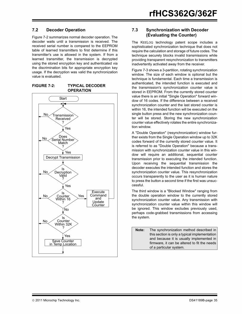
7.2 Decoder OperationFigure 7-2 summarizes normal decoder operation. Thedecoder waits until a transmission is received. Thereceived serial number is compared to the EEPROMtable of learned transmitters to first determine if thistransmitter's use is allowed in the system. If from alearned transmitter, the transmission is decryptedusing the stored encryption key and authenticated viathe discrimination bits for appropriate encryption keyusage. If the decryption was valid the synchronizationvalue is evaluated.FIGURE 7-2: TYPICAL DECODER OPERATION
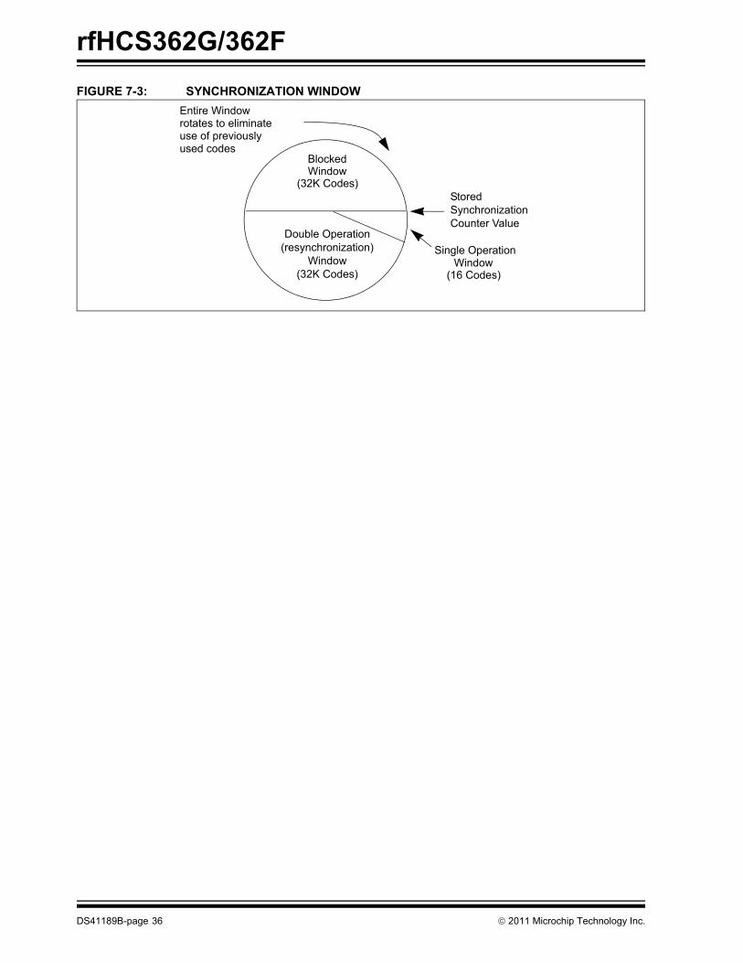
7.3 Synchronization with Decoder (Evaluating the Counter)
The KEELOQ technology patent scope includes asophisticated synchronization technique that does notrequire the calculation and storage of future codes. Thetechnique securely blocks invalid transmissions whileproviding transparent resynchronization to transmittersinadvertently activated away from the receiver.
Figure 7-3 shows a 3-partition, rotating synchronizationwindow. The size of each window is optional but thetechnique is fundamental. Each time a transmission isauthenticated, the intended function is executed andthe transmission's synchronization counter value isstored in EEPROM. From the currently stored countervalue there is an initial "Single Operation" forward win-dow of 16 codes. If the difference between a receivedsynchronization counter and the last stored counter iswithin 16, the intended function will be executed on thesingle button press and the new synchronization coun-ter will be stored. Storing the new synchronizationcounter value effectively rotates the entire synchroniza-tion window.
A "Double Operation" (resynchronization) window fur-ther exists from the Single Operation window up to 32Kcodes forward of the currently stored counter value. Itis referred to as "Double Operation" because a trans-mission with synchronization counter value in this win-dow will require an additional, sequential countertransmission prior to executing the intended function.Upon receiving the sequential transmission thedecoder executes the intended function and stores thesynchronization counter value. This resynchronizationoccurs transparently to the user as it is human natureto press the button a second time if the first was unsuc-cessful.
The third window is a "Blocked Window" ranging fromthe double operation window to the currently storedsynchronization counter value. Any transmission withsynchronization counter value within this window willbe ignored. This window excludes previously used,perhaps code-grabbed transmissions from accessingthe system.
?
TransmissionReceived
DoesSerial Number
Match?
Decrypt Transmission
IsDecryption
Valid?
IsCounter
Within 16?
IsCounter
Within 32K?
UpdateCounter
ExecuteCommand
Save Counterin Temp Location
Start
No
No
No
No
Yes
Yes
Yes
Yes
Yes
No
andNo
Note: The synchronization method described inthis section is only a typical implementationand because it is usually implemented infirmware, it can be altered to fit the needsof a particular system.
© 2011 Microchip Technology Inc. DS41189B-page 35
rfHCS362G/362F
FIGURE 7-3: SYNCHRONIZATION WINDOWBlocked
Entire Window rotates to eliminateuse of previouslyused codes
Single OperationWindow
Window(32K Codes)
(16 Codes)
Double Operation(resynchronization)
Window (32K Codes)
StoredSynchronizationCounter Value
DS41189B-page 36 © 2011 Microchip Technology Inc.
rfHCS362G/362F
8.0 DEVELOPMENT SUPPORTThe PIC® microcontrollers and dsPIC® digital signalcontrollers are supported with a full range of softwareand hardware development tools:
• Integrated Development Environment- MPLAB® IDE Software
• Compilers/Assemblers/Linkers- MPLAB C Compiler for Various Device
Families- HI-TECH C for Various Device Families- MPASMTM Assembler- MPLINKTM Object Linker/
MPLIBTM Object Librarian- MPLAB Assembler/Linker/Librarian for
Various Device Families• Simulators
- MPLAB SIM Software Simulator• Emulators
- MPLAB REAL ICE™ In-Circuit Emulator• In-Circuit Debuggers
- MPLAB ICD 3- PICkit™ 3 Debug Express
• Device Programmers- PICkit™ 2 Programmer- MPLAB PM3 Device Programmer
• Low-Cost Demonstration/Development Boards, Evaluation Kits, and Starter Kits
8.1 MPLAB Integrated Development Environment Software
The MPLAB IDE software brings an ease of softwaredevelopment previously unseen in the 8/16/32-bitmicrocontroller market. The MPLAB IDE is a Windows®
operating system-based application that contains:
• A single graphical interface to all debugging tools- Simulator- Programmer (sold separately)- In-Circuit Emulator (sold separately)- In-Circuit Debugger (sold separately)
• A full-featured editor with color-coded context• A multiple project manager• Customizable data windows with direct edit of
contents• High-level source code debugging• Mouse over variable inspection• Drag and drop variables from source to watch
windows• Extensive on-line help• Integration of select third party tools, such as
IAR C Compilers
The MPLAB IDE allows you to:
• Edit your source files (either C or assembly)• One-touch compile or assemble, and download to
emulator and simulator tools (automatically updates all project information)
• Debug using:- Source files (C or assembly)- Mixed C and assembly- Machine code
MPLAB IDE supports multiple debugging tools in asingle development paradigm, from the cost-effectivesimulators, through low-cost in-circuit debuggers, tofull-featured emulators. This eliminates the learningcurve when upgrading to tools with increased flexibilityand power.
© 2011 Microchip Technology Inc. DS41189B-page 37
rfHCS362G/362F
8.2 MPLAB C Compilers for VariousDevice FamiliesThe MPLAB C Compiler code development systemsare complete ANSI C compilers for Microchip’s PIC18,PIC24 and PIC32 families of microcontrollers and thedsPIC30 and dsPIC33 families of digital signal control-lers. These compilers provide powerful integrationcapabilities, superior code optimization and ease ofuse.
For easy source level debugging, the compilers providesymbol information that is optimized to the MPLAB IDEdebugger.
8.3 HI-TECH C for Various Device Families
The HI-TECH C Compiler code development systemsare complete ANSI C compilers for Microchip’s PICfamily of microcontrollers and the dsPIC family of digitalsignal controllers. These compilers provide powerfulintegration capabilities, omniscient code generationand ease of use.
For easy source level debugging, the compilers providesymbol information that is optimized to the MPLAB IDEdebugger.
The compilers include a macro assembler, linker, pre-processor, and one-step driver, and can run on multipleplatforms.
8.4 MPASM AssemblerThe MPASM Assembler is a full-featured, universalmacro assembler for PIC10/12/16/18 MCUs.
The MPASM Assembler generates relocatable objectfiles for the MPLINK Object Linker, Intel® standard HEXfiles, MAP files to detail memory usage and symbolreference, absolute LST files that contain source linesand generated machine code and COFF files fordebugging.
The MPASM Assembler features include:
• Integration into MPLAB IDE projects• User-defined macros to streamline
assembly code• Conditional assembly for multi-purpose
source files• Directives that allow complete control over the
assembly process
8.5 MPLINK Object Linker/MPLIB Object Librarian
The MPLINK Object Linker combines relocatableobjects created by the MPASM Assembler and theMPLAB C18 C Compiler. It can link relocatable objectsfrom precompiled libraries, using directives from alinker script.
The MPLIB Object Librarian manages the creation andmodification of library files of precompiled code. Whena routine from a library is called from a source file, onlythe modules that contain that routine will be linked inwith the application. This allows large libraries to beused efficiently in many different applications.
The object linker/library features include:
• Efficient linking of single libraries instead of many smaller files
• Enhanced code maintainability by grouping related modules together
• Flexible creation of libraries with easy module listing, replacement, deletion and extraction
8.6 MPLAB Assembler, Linker and Librarian for Various Device Families
MPLAB Assembler produces relocatable machinecode from symbolic assembly language for PIC24,PIC32 and dsPIC devices. MPLAB C Compiler usesthe assembler to produce its object file. The assemblergenerates relocatable object files that can then bearchived or linked with other relocatable object files andarchives to create an executable file. Notable featuresof the assembler include:
• Support for the entire device instruction set• Support for fixed-point and floating-point data• Command line interface• Rich directive set• Flexible macro language• MPLAB IDE compatibility
DS41189B-page 38 © 2011 Microchip Technology Inc.
rfHCS362G/362F
8.7 MPLAB SIM Software SimulatorThe MPLAB SIM Software Simulator allows codedevelopment in a PC-hosted environment by simulat-ing the PIC MCUs and dsPIC® DSCs on an instructionlevel. On any given instruction, the data areas can beexamined or modified and stimuli can be applied froma comprehensive stimulus controller. Registers can belogged to files for further run-time analysis. The tracebuffer and logic analyzer display extend the power ofthe simulator to record and track program execution,actions on I/O, most peripherals and internal registers.The MPLAB SIM Software Simulator fully supportssymbolic debugging using the MPLAB C Compilers,and the MPASM and MPLAB Assemblers. The soft-ware simulator offers the flexibility to develop anddebug code outside of the hardware laboratory envi-ronment, making it an excellent, economical softwaredevelopment tool.
8.8 MPLAB REAL ICE In-Circuit Emulator System
MPLAB REAL ICE In-Circuit Emulator System isMicrochip’s next generation high-speed emulator forMicrochip Flash DSC and MCU devices. It debugs andprograms PIC® Flash MCUs and dsPIC® Flash DSCswith the easy-to-use, powerful graphical user interface ofthe MPLAB Integrated Development Environment (IDE),included with each kit.
The emulator is connected to the design engineer’s PCusing a high-speed USB 2.0 interface and is connectedto the target with either a connector compatible with in-circuit debugger systems (RJ11) or with the new high-speed, noise tolerant, Low-Voltage Differential Signal(LVDS) interconnection (CAT5).
The emulator is field upgradable through future firmwaredownloads in MPLAB IDE. In upcoming releases ofMPLAB IDE, new devices will be supported, and newfeatures will be added. MPLAB REAL ICE offerssignificant advantages over competitive emulatorsincluding low-cost, full-speed emulation, run-timevariable watches, trace analysis, complex breakpoints, aruggedized probe interface and long (up to three meters)interconnection cables.
8.9 MPLAB ICD 3 In-Circuit Debugger System
MPLAB ICD 3 In-Circuit Debugger System is Micro-chip's most cost effective high-speed hardwaredebugger/programmer for Microchip Flash Digital Sig-nal Controller (DSC) and microcontroller (MCU)devices. It debugs and programs PIC® Flash microcon-trollers and dsPIC® DSCs with the powerful, yet easy-to-use graphical user interface of MPLAB IntegratedDevelopment Environment (IDE).
The MPLAB ICD 3 In-Circuit Debugger probe is con-nected to the design engineer's PC using a high-speedUSB 2.0 interface and is connected to the target with aconnector compatible with the MPLAB ICD 2 or MPLABREAL ICE systems (RJ-11). MPLAB ICD 3 supports allMPLAB ICD 2 headers.
8.10 PICkit 3 In-Circuit Debugger/Programmer and PICkit 3 Debug Express
The MPLAB PICkit 3 allows debugging and program-ming of PIC® and dsPIC® Flash microcontrollers at amost affordable price point using the powerful graphicaluser interface of the MPLAB Integrated DevelopmentEnvironment (IDE). The MPLAB PICkit 3 is connectedto the design engineer's PC using a full speed USBinterface and can be connected to the target via anMicrochip debug (RJ-11) connector (compatible withMPLAB ICD 3 and MPLAB REAL ICE). The connectoruses two device I/O pins and the reset line to imple-ment in-circuit debugging and In-Circuit Serial Pro-gramming™.
The PICkit 3 Debug Express include the PICkit 3, demoboard and microcontroller, hookup cables and CDROMwith user’s guide, lessons, tutorial, compiler andMPLAB IDE software.
© 2011 Microchip Technology Inc. DS41189B-page 39
rfHCS362G/362F
8.11 PICkit 2 DevelopmentProgrammer/Debugger and PICkit 2 Debug Express
The PICkit™ 2 Development Programmer/Debugger isa low-cost development tool with an easy to use inter-face for programming and debugging Microchip’s Flashfamilies of microcontrollers. The full featuredWindows® programming interface supports baseline(PIC10F, PIC12F5xx, PIC16F5xx), midrange(PIC12F6xx, PIC16F), PIC18F, PIC24, dsPIC30,dsPIC33, and PIC32 families of 8-bit, 16-bit, and 32-bitmicrocontrollers, and many Microchip Serial EEPROMproducts. With Microchip’s powerful MPLAB IntegratedDevelopment Environment (IDE) the PICkit™ 2enables in-circuit debugging on most PIC® microcon-trollers. In-Circuit-Debugging runs, halts and singlesteps the program while the PIC microcontroller isembedded in the application. When halted at a break-point, the file registers can be examined and modified.
The PICkit 2 Debug Express include the PICkit 2, demoboard and microcontroller, hookup cables and CDROMwith user’s guide, lessons, tutorial, compiler andMPLAB IDE software.
8.12 MPLAB PM3 Device ProgrammerThe MPLAB PM3 Device Programmer is a universal,CE compliant device programmer with programmablevoltage verification at VDDMIN and VDDMAX formaximum reliability. It features a large LCD display(128 x 64) for menus and error messages and a modu-lar, detachable socket assembly to support variouspackage types. The ICSP™ cable assembly is includedas a standard item. In Stand-Alone mode, the MPLABPM3 Device Programmer can read, verify and programPIC devices without a PC connection. It can also setcode protection in this mode. The MPLAB PM3connects to the host PC via an RS-232 or USB cable.The MPLAB PM3 has high-speed communications andoptimized algorithms for quick programming of largememory devices and incorporates an MMC card for filestorage and data applications.
8.13 Demonstration/Development Boards, Evaluation Kits, and Starter Kits
A wide variety of demonstration, development andevaluation boards for various PIC MCUs and dsPICDSCs allows quick application development on fully func-tional systems. Most boards include prototyping areas foradding custom circuitry and provide application firmwareand source code for examination and modification.
The boards support a variety of features, including LEDs,temperature sensors, switches, speakers, RS-232interfaces, LCD displays, potentiometers and additionalEEPROM memory.
The demonstration and development boards can beused in teaching environments, for prototyping customcircuits and for learning about various microcontrollerapplications.
In addition to the PICDEM™ and dsPICDEM™ demon-stration/development board series of circuits, Microchiphas a line of evaluation kits and demonstration softwarefor analog filter design, KEELOQ® security ICs, CAN,IrDA®, PowerSmart battery management, SEEVAL®
evaluation system, Sigma-Delta ADC, flow ratesensing, plus many more.
Also available are starter kits that contain everythingneeded to experience the specified device. This usuallyincludes a single application and debug capability, allon one board.
Check the Microchip web page (www.microchip.com)for the complete list of demonstration, developmentand evaluation kits.
DS41189B-page 40 © 2011 Microchip Technology Inc.
rfHCS362G/362F
9.0 ELECTRICAL CHARACTERISTICSAbsolute Maximum Ratings†Ambient Temperature under bias.............................................................................................................. -40°C to +85°C
Storage Temperature .............................................................................................................................. -40°C to +125°C
Total Power Dissipation(1) ....................................................................................................................................700 mW
Absolute Maximum Ratings Encoder Voltage on VDD with respect to VSS ..............................................................................................................-0.3 to +6.6V
Max. Output Current sunk by any I/O pin................................................................................................................20 mA
Max. Output Current sourced by any I/O pin...........................................................................................................20 mA
Voltage on all other Encoder pins with respect to VSS................................................................... -0.3 V to (VDD + 0.3V)
Absolute Maximum Ratings TransmitterVoltage on VDDRF with respect to VSSRF ......................................................................................................-0.3 to +7.0V
Max. Voltage on RFENIN and DATAFSK pins with respect to VSSRF ...............................................-0.3 to (VDDRF +0.3V)
Max. Current into RFENIN and DATAFSK pins.............................................................................................-1.0 to 1.0 mA
Note 1: Power Dissipation is calculated as follows:
PDIS = VDD x {IDD - ∑ IOH} + ∑ {(VDD-VOH) x IOH} + ∑(VOL x IOL) + VDDRF x {IDDRF - ∑ IOHRF} + ∑ {(VDDRF-VOHRF) x IOHRF} †NOTICE: Stresses above those listed under "Absolute Maximum Ratings" may cause permanent damage to thedevice. This is a stress rating only and functional operation of the device at those or any other conditions abovethose indicated in the operation listings of this specification is not implied. Exposure to maximum rating conditionsfor extended periods may affect device reliability.
© 2011 Microchip Technology Inc. DS41189B-page 41
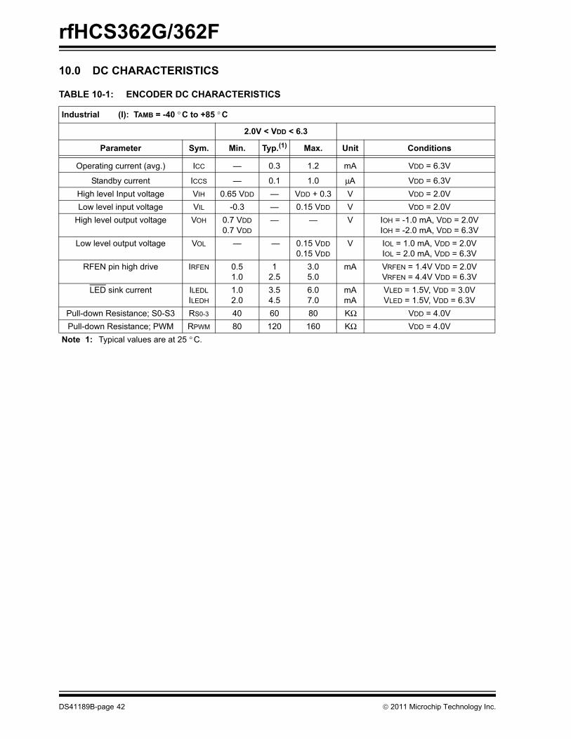
rfHCS362G/362F
10.0 DC CHARACTERISTICS
TABLE 10-1: ENCODER DC CHARACTERISTICS
Industrial (I): TAMB = -40 ° C to +85 ° C
2.0V < VDD < 6.3
Parameter Sym. Min. Typ.(1) Max. Unit Conditions
Operating current (avg.) ICC — 0.3 1.2 mA VDD = 6.3V
Standby current ICCS — 0.1 1.0 μA VDD = 6.3VHigh level Input voltage VIH 0.65 VDD — VDD + 0.3 V VDD = 2.0VLow level input voltage VIL -0.3 — 0.15 VDD V VDD = 2.0V
High level output voltage VOH 0.7 VDD0.7 VDD
— — V IOH = -1.0 mA, VDD = 2.0VIOH = -2.0 mA, VDD = 6.3V
Low level output voltage VOL — — 0.15 VDD0.15 VDD
V IOL = 1.0 mA, VDD = 2.0VIOL = 2.0 mA, VDD = 6.3V
RFEN pin high drive IRFEN 0.51.0
12.5
3.05.0
mA VRFEN = 1.4V VDD = 2.0VVRFEN = 4.4V VDD = 6.3V
LED sink current ILEDLILEDH
1.02.0
3.54.5
6.07.0
mAmA
VLED = 1.5V, VDD = 3.0VVLED = 1.5V, VDD = 6.3V
Pull-down Resistance; S0-S3 RS0-3 40 60 80 KΩ VDD = 4.0VPull-down Resistance; PWM RPWM 80 120 160 KΩ VDD = 4.0V
Note 1: Typical values are at 25 ° C.
DS41189B-page 42 © 2011 Microchip Technology Inc.
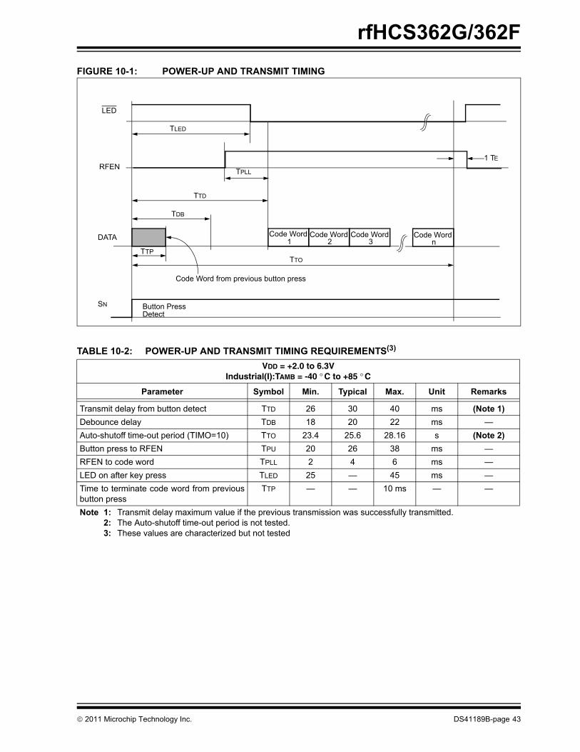
rfHCS362G/362F
FIGURE 10-1: POWER-UP AND TRANSMIT TIMINGTABLE 10-2: POWER-UP AND TRANSMIT TIMING REQUIREMENTS(3)
VDD = +2.0 to 6.3VIndustrial(I):TAMB = -40 ° C to +85 ° C
Parameter Symbol Min. Typical Max. Unit Remarks
Transmit delay from button detect TTD 26 30 40 ms (Note 1)Debounce delay TDB 18 20 22 ms —Auto-shutoff time-out period (TIMO=10) TTO 23.4 25.6 28.16 s (Note 2)Button press to RFEN TPU 20 26 38 ms —RFEN to code word TPLL 2 4 6 ms —LED on after key press TLED 25 — 45 ms —Time to terminate code word from previousbutton press
TTP — — 10 ms — —
Note 1: Transmit delay maximum value if the previous transmission was successfully transmitted.2: The Auto-shutoff time-out period is not tested.3: These values are characterized but not tested
SN
TDB
DATA
TTD
TTO
Code Word 1
Code Word 2
Code Word 3
Code Word n
TTP
Button Press Detect
RFEN
LED
TPLL
TLED
1 TE
Code Word from previous button press
© 2011 Microchip Technology Inc. DS41189B-page 43
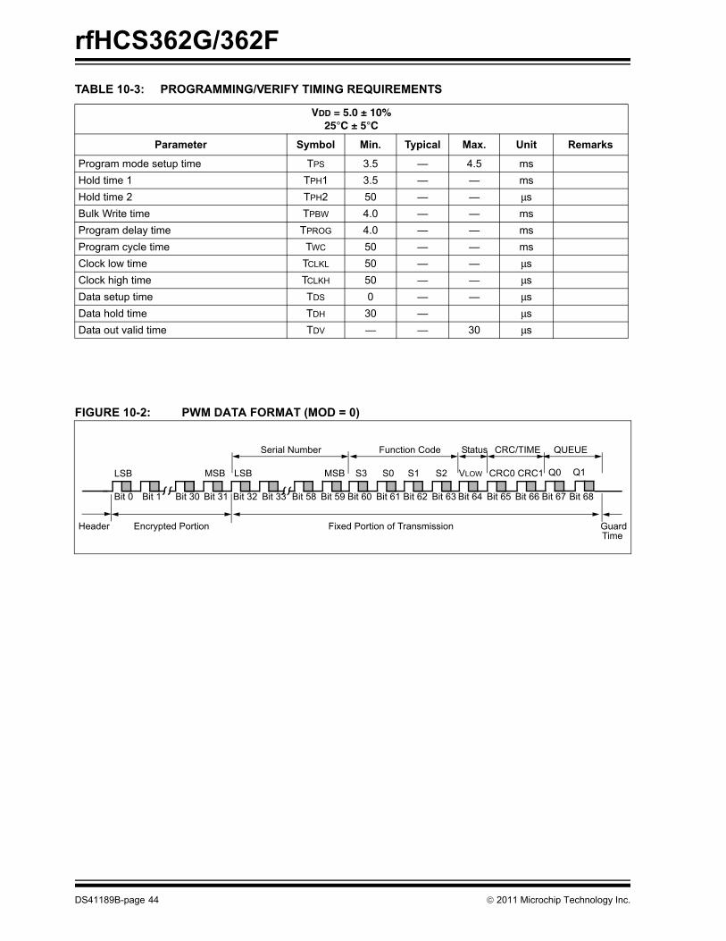
rfHCS362G/362F
TABLE 10-3: PROGRAMMING/VERIFY TIMING REQUIREMENTSFIGURE 10-2: PWM DATA FORMAT (MOD = 0)
VDD = 5.0 ± 10%25°C ± 5°C
Parameter Symbol Min. Typical Max. Unit Remarks
Program mode setup time TPS 3.5 — 4.5 msHold time 1 TPH1 3.5 — — msHold time 2 TPH2 50 — — μsBulk Write time TPBW 4.0 — — msProgram delay time TPROG 4.0 — — msProgram cycle time TWC 50 — — msClock low time TCLKL 50 — — μsClock high time TCLKH 50 — — μsData setup time TDS 0 — — μsData hold time TDH 30 — μsData out valid time TDV — — 30 μs
Bit 0 Bit 1
Header
Bit 30 Bit 31 Bit 32 Bit 33 Bit 58 Bit 59
Fixed Portion of TransmissionEncrypted Portion Guard
LSBLSB MSB MSB S3 S0 S1 S2 VLOW CRC0 CRC1
Time
Serial Number Function Code Status
Bit 60 Bit 61 Bit 62 Bit 63 Bit 64 Bit 65
CRC/TIME
Bit 66
QUEUE
Q0 Q1
Bit 67 Bit 68
DS41189B-page 44 © 2011 Microchip Technology Inc.
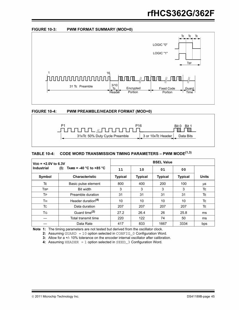
rfHCS362G/362F
FIGURE 10-3: PWM FORMAT SUMMARY (MOD=0)FIGURE 10-4: PWM PREAMBLE/HEADER FORMAT (MOD=0)
TABLE 10-4: CODE WORD TRANSMISSION TIMING PARAMETERS – PWM MODE(1,3)
VDD = +2.0V to 6.3VIndustrial (I): TAMB = -40 °C to +85 °C
BSEL Value
11 10 01 00
Symbol Characteristic Typical Typical Typical Typical Units
TE Basic pulse element 800 400 200 100 μsTBP Bit width 3 3 3 3 TE
TP Preamble duration 31 31 31 31 TE
TH Header duration(4) 10 10 10 10 TE
TC Data duration 207 207 207 207 TE
TG Guard time(2) 27.2 26.4 26 25.8 ms— Total transmit time 220 122 74 50 ms— Data Rate 417 833 1667 3334 bps
Note 1: The timing parameters are not tested but derived from the oscillator clock.2: Assuming GUARD = 10 option selected in CONFIG_0 Configuration Word.3: Allow for a +/- 10% tolerance on the encoder internal oscillator after calibration.4: Assuming HEADER = 1 option selected in SEED_3 Configuration Word.
LOGIC "1"
GuardTime
31 TE EncryptedPortion
Fixed Code Portion
LOGIC "0"
Preamble 3/10
Header
TE TE TE
TE
1 16
TBP
50% Duty Cycle Preamble
P1 P16
31xTE 3 or 10xTE Header Data Bits
Bit 0 Bit 1
© 2011 Microchip Technology Inc. DS41189B-page 45
rfHCS362G/362F
FIGURE 10-5: MANCHESTER FORMAT SUMMARY (MOD=1)FIGURE 10-6: MANCHESTER PREAMBLE/HEADER FORMAT (MOD=1)
TABLE 10-5: CODE WORD TRANSMISSION TIMING PARAMETERS—MANCHESTER MODE(1,3)
VDD = +2.0V to 6.3VIndustrial (I): TAMB = -40 °C to +85 °C
BSEL Value
11 10 01 00
Symbol Characteristic Typical Typical Typical Typical Units
TE Basic pulse element(3) 800 400 200 100 μsTBP Bit width 2 2 2 2 TE
TP Preamble duration 31 31 31 31 TE
TH Header duration 4 4 4 4 TE
TC Data duration 138 138 138 138 TE
TG Guard time(2) 26.8 26.4 26 25.8 ms— Total transmit time 166 96 61 43 ms— Data Rate 625 1250 2500 5000 bps
Note 1: The timing parameters are not tested but derived from the oscillator clock.2: Assuming GUARD = 10 option selected in CONFIG_0 Configuration Word.3: Allow for a +/- 10% tolerance on the encoder internal oscillator after calibration.
GuardPreamble Header Encrypted Fixed Code
1 2
START bitSTOP bit
TimePortion Portion
16 bit 0 bit 1 bit 2
LOGIC "0"
LOGIC "1"
TE TE
TBP
Preamble Header31 x TE4 x TE
Bit 0 Bit 1
Data Word Transmission
P1 P16
DS41189B-page 46 © 2011 Microchip Technology Inc.
rfHCS362G/362F
TABLE 10-6: TRANSMITTER DC CHARACTERISTICS** These parameters are characterized but not tested.† Data in “Typ” column is at 3V, 25°C unless otherwise stated. These parameters are for design guidance only
and are not tested.Note 1: Depends on output power selection. See Table 6-6.Note 2: Applies to RFEN pin.
TABLE 10-7: TRANSMITTER AC CHARACTERISTICS*
bit * These parameters are characterized but not tested.† Data in “Typ” column is at 3V, 25°C unless otherwise stated. These parameters are for design guidance only
and are not tested.Note 1: Values dependent on PLL loop filter values.
Note 2: ton equals crystal oscillator and PLL start-up time.
Note 3: Max FSK data rate requires crystal with appropriate motional parameters. See Section 6.3.
DC CHARACTERISTICS Standard Operating Conditions (unless otherwise stated)Operating Temperature -40°C ≤ TA ≤ +85°C
ParamNo. Sym Characteristic Min Typ† Max Units Conditions
VDDRF Supply Voltage 2.2 — 5.5 VIPDRF Power-Down Current — 0.05 0.1 μA RFEN = 0IDDRF Supply Current 4.8 — 11.5 mA Note 1VILRF Input Low Voltage -0.3 — 0.3 VSSRF V Note 2VIHRF Input High Voltage 0.7 VSSRF — VSSRF + 0.3 V Note 2IILRF Input Leakage Current -1 — 1 μA
AC CHARACTERISTICS Standard Operating Conditions (unless otherwise stated)Operating Temperature -40°C ≤ TA ≤ +85°C
ParamNo. Sym Characteristic Min Typ† Max Units Conditions
fxtal Crystal Frequency 9.69 — 15 MHzftransmit Transmit Frequency 310 — 440 MHz Fixed, set by fxtalfCLKOUT CLKOUT Frequency 2.42 — 3.75 MHz Fixed, set by fxtal
Po Transmit Output Power -12 — +2 dBm See Table 6-6fASK ASK Data Rate — — 40 kbpsfFSK FSK Data Rate — — 20 kbps Note 3PREF Reference Spurs (1) — -44 — dBm ftransmit ± fxtalPCLK Clock Spurs (1) — -44 — dBm ftransmit ± fCLKOUT
PHARM Harmonic Content — -40 — dBm 2ftransmit, 3ftransmit, 4ftransmit,...
POFF Spurious Output Signal — -60 — dBm Vps ≤ 0.1VPN Phase Noise — -87 — dBc/Hz ftransmit ± 500 kHz
KVCO VCO Gain — 100 — MHz/VICP Charge Pump Current — ±260 — μA
VCLKOUT Clock Voltage Swing — 2 — VPP Cload = 5 pFton Start-up Time — 0.9 — ms Note 2
© 2011 Microchip Technology Inc. DS41189B-page 47
rfHCS362G/362F
APPENDIX A: ADDITIONAL INFORMATION
Microchip’s Secure Data Products are covered bysome or all of the following:
Code hopping encoder patents issued in Europeancountries and U.S.A.
Secure learning patents issued in European countries,U.S.A. and R.S.A.
REVISION HISTORY
Revision B (June 2011)• Updated the following sections: Development Sup-
port, The Microchip Web Site, Reader Response and rfHCS362G/362F Product Identification System
• Added new section Appendix A• Minor formatting and text changes were incorporated
throughout the document
DS41189B-page 48 © 2011 Microchip Technology Inc.
rfHCS362G/362F
THE MICROCHIP WEB SITEMicrochip provides online support via our WWW site atwww.microchip.com. This web site is used as a meansto make files and information easily available tocustomers. Accessible by using your favorite Internetbrowser, the web site contains the followinginformation:
• Product Support – Data sheets and errata, application notes and sample programs, design resources, user’s guides and hardware support documents, latest software releases and archived software
• General Technical Support – Frequently Asked Questions (FAQ), technical support requests, online discussion groups, Microchip consultant program member listing
• Business of Microchip – Product selector and ordering guides, latest Microchip press releases, listing of seminars and events, listings of Microchip sales offices, distributors and factory representatives
CUSTOMER CHANGE NOTIFICATION SERVICEMicrochip’s customer notification service helps keepcustomers current on Microchip products. Subscriberswill receive e-mail notification whenever there arechanges, updates, revisions or errata related to aspecified product family or development tool of interest.
To register, access the Microchip web site atwww.microchip.com. Under “Support”, click on“Customer Change Notification” and follow theregistration instructions.
CUSTOMER SUPPORTUsers of Microchip products can receive assistancethrough several channels:
• Distributor or Representative• Local Sales Office• Field Application Engineer (FAE)• Technical Support• Development Systems Information Line
Customers should contact their distributor,representative or field application engineer (FAE) forsupport. Local sales offices are also available to helpcustomers. A listing of sales offices and locations isincluded in the back of this document.
Technical support is available through the web siteat: http://microchip.com/support
© 2011 Microchip Technology Inc. DS41189B-page 49

rfHCS362G/362F
READER RESPONSEIt is our intention to provide you with the best documentation possible to ensure successful use of your Microchipproduct. If you wish to provide your comments on organization, clarity, subject matter, and ways in which ourdocumentation can better serve you, please FAX your comments to the Technical Publications Manager at(480) 792-4150.
Please list the following information, and use this outline to provide us with your comments about this document.
TO: Technical Publications ManagerRE: Reader Response
Total Pages Sent ________
From: Name
CompanyAddressCity / State / ZIP / Country
Telephone: (_______) _________ - _________
Application (optional):
Would you like a reply? Y N
Device: Literature Number:
Questions:
FAX: (______) _________ - _________
DS41189BrfHCS362G/362F
1. What are the best features of this document?
2. How does this document meet your hardware and software development needs?
3. Do you find the organization of this document easy to follow? If not, why?
4. What additions to the document do you think would enhance the structure and subject?
5. What deletions from the document could be made without affecting the overall usefulness?
6. Is there any incorrect or misleading information (what and where)?
7. How would you improve this document?
DS41189B-page 50 © 2011 Microchip Technology Inc.
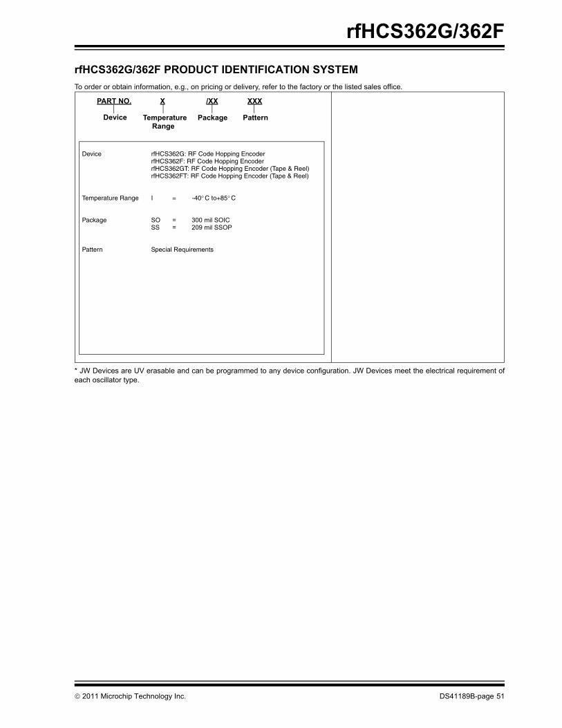
rfHCS362G/362F
rfHCS362G/362F PRODUCT IDENTIFICATION SYSTEMTo order or obtain information, e.g., on pricing or delivery, refer to the factory or the listed sales office.
* JW Devices are UV erasable and can be programmed to any device configuration. JW Devices meet the electrical requirement ofeach oscillator type.
PART NO. X /XX XXX
PatternPackageTemperatureRange
Device
Device rfHCS362G: RF Code Hopping EncoderrfHCS362F: RF Code Hopping EncoderrfHCS362GT: RF Code Hopping Encoder (Tape & Reel)rfHCS362FT: RF Code Hopping Encoder (Tape & Reel)
Temperature Range I = -40° C to+85° C
Package SO = 300 mil SOICSS = 209 mil SSOP
Pattern Special Requirements
© 2011 Microchip Technology Inc. DS41189B-page 51
rfHCS362G/362F
NOTES:DS41189B-page 52 © 2011 Microchip Technology Inc.
Note the following details of the code protection feature on Microchip devices:• Microchip products meet the specification contained in their particular Microchip Data Sheet.
• Microchip believes that its family of products is one of the most secure families of its kind on the market today, when used in the intended manner and under normal conditions.
• There are dishonest and possibly illegal methods used to breach the code protection feature. All of these methods, to our knowledge, require using the Microchip products in a manner outside the operating specifications contained in Microchip’s Data Sheets. Most likely, the person doing so is engaged in theft of intellectual property.
• Microchip is willing to work with the customer who is concerned about the integrity of their code.
• Neither Microchip nor any other semiconductor manufacturer can guarantee the security of their code. Code protection does not mean that we are guaranteeing the product as “unbreakable.”
Code protection is constantly evolving. We at Microchip are committed to continuously improving the code protection features of ourproducts. Attempts to break Microchip’s code protection feature may be a violation of the Digital Millennium Copyright Act. If such actsallow unauthorized access to your software or other copyrighted work, you may have a right to sue for relief under that Act.
Information contained in this publication regarding deviceapplications and the like is provided only for your convenienceand may be superseded by updates. It is your responsibility toensure that your application meets with your specifications.MICROCHIP MAKES NO REPRESENTATIONS ORWARRANTIES OF ANY KIND WHETHER EXPRESS ORIMPLIED, WRITTEN OR ORAL, STATUTORY OROTHERWISE, RELATED TO THE INFORMATION,INCLUDING BUT NOT LIMITED TO ITS CONDITION,QUALITY, PERFORMANCE, MERCHANTABILITY ORFITNESS FOR PURPOSE. Microchip disclaims all liabilityarising from this information and its use. Use of Microchipdevices in life support and/or safety applications is entirely atthe buyer’s risk, and the buyer agrees to defend, indemnify andhold harmless Microchip from any and all damages, claims,suits, or expenses resulting from such use. No licenses areconveyed, implicitly or otherwise, under any Microchipintellectual property rights.
© 2011 Microchip Technology Inc.
Trademarks
The Microchip name and logo, the Microchip logo, dsPIC, KEELOQ, KEELOQ logo, MPLAB, PIC, PICmicro, PICSTART, PIC32 logo, rfPIC and UNI/O are registered trademarks of Microchip Technology Incorporated in the U.S.A. and other countries.
FilterLab, Hampshire, HI-TECH C, Linear Active Thermistor, MXDEV, MXLAB, SEEVAL and The Embedded Control Solutions Company are registered trademarks of Microchip Technology Incorporated in the U.S.A.
Analog-for-the-Digital Age, Application Maestro, CodeGuard, dsPICDEM, dsPICDEM.net, dsPICworks, dsSPEAK, ECAN, ECONOMONITOR, FanSense, HI-TIDE, In-Circuit Serial Programming, ICSP, Mindi, MiWi, MPASM, MPLAB Certified logo, MPLIB, MPLINK, mTouch, Omniscient Code Generation, PICC, PICC-18, PICDEM, PICDEM.net, PICkit, PICtail, REAL ICE, rfLAB, Select Mode, Total Endurance, TSHARC, UniWinDriver, WiperLock and ZENA are trademarks of Microchip Technology Incorporated in the U.S.A. and other countries.
SQTP is a service mark of Microchip Technology Incorporated in the U.S.A.
All other trademarks mentioned herein are property of their respective companies.
© 2011, Microchip Technology Incorporated, Printed in the U.S.A., All Rights Reserved.
Printed on recycled paper.
ISBN: 978-1-61341-234-3
DS41189B-page 53
Microchip received ISO/TS-16949:2002 certification for its worldwide headquarters, design and wafer fabrication facilities in Chandler and Tempe, Arizona; Gresham, Oregon and design centers in California and India. The Company’s quality system processes and procedures are for its PIC® MCUs and dsPIC® DSCs, KEELOQ® code hopping devices, Serial EEPROMs, microperipherals, nonvolatile memory and analog products. In addition, Microchip’s quality system for the design and manufacture of development systems is ISO 9001:2000 certified.
DS41189B-page 54 © 2011 Microchip Technology Inc.
AMERICASCorporate Office2355 West Chandler Blvd.Chandler, AZ 85224-6199Tel: 480-792-7200 Fax: 480-792-7277Technical Support: http://www.microchip.com/supportWeb Address: www.microchip.comAtlantaDuluth, GA Tel: 678-957-9614 Fax: 678-957-1455BostonWestborough, MA Tel: 774-760-0087 Fax: 774-760-0088ChicagoItasca, IL Tel: 630-285-0071 Fax: 630-285-0075ClevelandIndependence, OH Tel: 216-447-0464 Fax: 216-447-0643DallasAddison, TX Tel: 972-818-7423 Fax: 972-818-2924DetroitFarmington Hills, MI Tel: 248-538-2250Fax: 248-538-2260IndianapolisNoblesville, IN Tel: 317-773-8323Fax: 317-773-5453Los AngelesMission Viejo, CA Tel: 949-462-9523 Fax: 949-462-9608Santa ClaraSanta Clara, CA Tel: 408-961-6444Fax: 408-961-6445TorontoMississauga, Ontario, CanadaTel: 905-673-0699 Fax: 905-673-6509
ASIA/PACIFICAsia Pacific OfficeSuites 3707-14, 37th FloorTower 6, The GatewayHarbour City, KowloonHong KongTel: 852-2401-1200Fax: 852-2401-3431Australia - SydneyTel: 61-2-9868-6733Fax: 61-2-9868-6755China - BeijingTel: 86-10-8569-7000 Fax: 86-10-8528-2104China - ChengduTel: 86-28-8665-5511Fax: 86-28-8665-7889China - ChongqingTel: 86-23-8980-9588Fax: 86-23-8980-9500China - HangzhouTel: 86-571-2819-3180 Fax: 86-571-2819-3189China - Hong Kong SARTel: 852-2401-1200 Fax: 852-2401-3431China - NanjingTel: 86-25-8473-2460Fax: 86-25-8473-2470China - QingdaoTel: 86-532-8502-7355Fax: 86-532-8502-7205China - ShanghaiTel: 86-21-5407-5533 Fax: 86-21-5407-5066China - ShenyangTel: 86-24-2334-2829Fax: 86-24-2334-2393China - ShenzhenTel: 86-755-8203-2660 Fax: 86-755-8203-1760China - WuhanTel: 86-27-5980-5300Fax: 86-27-5980-5118China - XianTel: 86-29-8833-7252Fax: 86-29-8833-7256China - XiamenTel: 86-592-2388138 Fax: 86-592-2388130China - ZhuhaiTel: 86-756-3210040 Fax: 86-756-3210049
ASIA/PACIFICIndia - BangaloreTel: 91-80-3090-4444 Fax: 91-80-3090-4123India - New DelhiTel: 91-11-4160-8631Fax: 91-11-4160-8632India - PuneTel: 91-20-2566-1512Fax: 91-20-2566-1513Japan - YokohamaTel: 81-45-471- 6166 Fax: 81-45-471-6122Korea - DaeguTel: 82-53-744-4301Fax: 82-53-744-4302Korea - SeoulTel: 82-2-554-7200Fax: 82-2-558-5932 or 82-2-558-5934Malaysia - Kuala LumpurTel: 60-3-6201-9857Fax: 60-3-6201-9859Malaysia - PenangTel: 60-4-227-8870Fax: 60-4-227-4068Philippines - ManilaTel: 63-2-634-9065Fax: 63-2-634-9069SingaporeTel: 65-6334-8870Fax: 65-6334-8850Taiwan - Hsin ChuTel: 886-3-6578-300Fax: 886-3-6578-370Taiwan - KaohsiungTel: 886-7-213-7830Fax: 886-7-330-9305Taiwan - TaipeiTel: 886-2-2500-6610 Fax: 886-2-2508-0102Thailand - BangkokTel: 66-2-694-1351Fax: 66-2-694-1350
EUROPEAustria - WelsTel: 43-7242-2244-39Fax: 43-7242-2244-393Denmark - CopenhagenTel: 45-4450-2828 Fax: 45-4485-2829France - ParisTel: 33-1-69-53-63-20 Fax: 33-1-69-30-90-79Germany - MunichTel: 49-89-627-144-0 Fax: 49-89-627-144-44Italy - Milan Tel: 39-0331-742611 Fax: 39-0331-466781Netherlands - DrunenTel: 31-416-690399 Fax: 31-416-690340Spain - MadridTel: 34-91-708-08-90Fax: 34-91-708-08-91UK - WokinghamTel: 44-118-921-5869Fax: 44-118-921-5820
Worldwide Sales and Service
05/02/11