Embed Size (px)
Citation preview
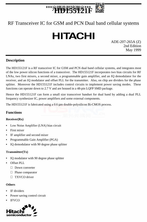
HD155121F
RF Transceiver IC for GSM and PCN Dual band cellular systems
ADE-207-265A (Z)2nd Edition
May 1999
Description
The HD155121F is a RF transceiver IC for GSM and PCN dual band cellular systems, and integrates mostof the low power silicon functions of a transceiver. The HD155121F incorporates two bias circuits for RFLNAs, two first mixers, a second mixer, a programmable gain amplifier, and an IQ demodulator for thereceiver, and an IQ modulator and offset PLL for the transmitter. Also, on chip are dividers for the phasesplitter. Moreover the HD155121F includes control circuits to implement power saving modes. Thesefunctions can operate down to 2.7 V and are housed in a 48-pin LQFP SMD package.
Hence the HD155121F can form a small size transceiver handset for dual band by adding a dual PLLfrequency synthesizer IC, power amplifiers and some external components.
The HD155121F is fabricated using a 0.6 µm double-polysilicon Bi-CMOS process.
Functions
Receiver(Rx)
• Low Noise Amplifier (LNA) bias circuit
• First mixer
• IF amplifier and second mixer
• Programmable Gain Amplifier (PGA)
• IQ demodulator with 90 degree phase splitter
Transmitter(Tx)
• IQ modulator with 90 degree phase splitter
• Offset PLL
Down converter
Phase comparator
TXVCO driver
Others
• IF dividers
• Power saving control circuit
• IFVCO
HD155121F
2
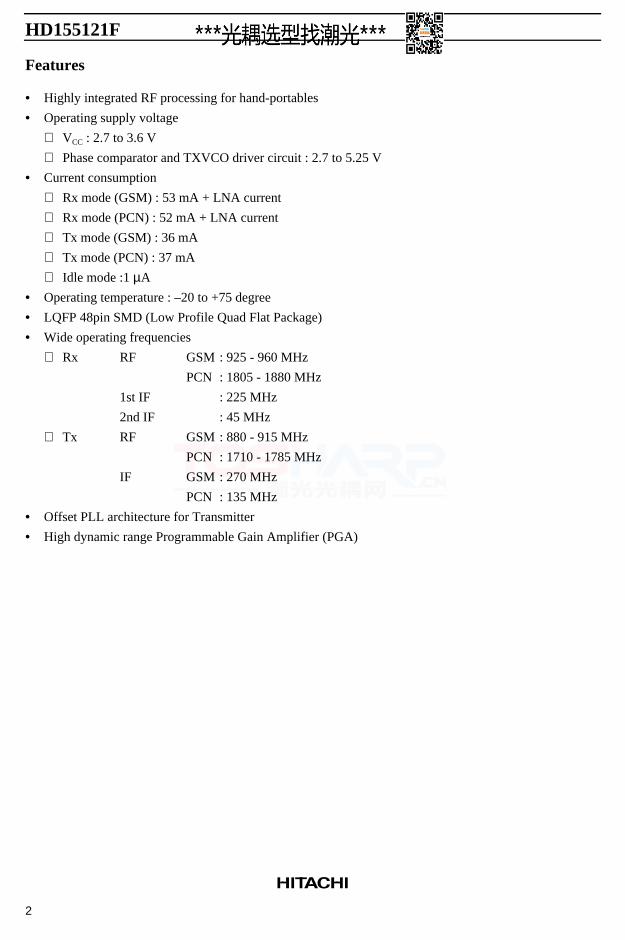
Features
• Highly integrated RF processing for hand-portables
• Operating supply voltage
VCC : 2.7 to 3.6 V
Phase comparator and TXVCO driver circuit : 2.7 to 5.25 V
• Current consumption
Rx mode (GSM) : 53 mA + LNA current
Rx mode (PCN) : 52 mA + LNA current
Tx mode (GSM) : 36 mA
Tx mode (PCN) : 37 mA
Idle mode :1 µA
• Operating temperature : –20 to +75 degree
• LQFP 48pin SMD (Low Profile Quad Flat Package)
• Wide operating frequencies
Rx RF GSM : 925 - 960 MHz
PCN : 1805 - 1880 MHz
1st IF : 225 MHz
2nd IF : 45 MHz
Tx RF GSM : 880 - 915 MHz
PCN : 1710 - 1785 MHz
IF GSM : 270 MHz
PCN : 135 MHz
• Offset PLL architecture for Transmitter
• High dynamic range Programmable Gain Amplifier (PGA)
HD155121F
3
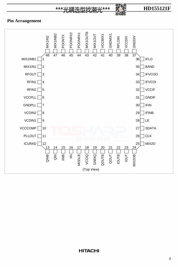
Pin Arrangement
1
2
3
4
5
6
7
8
9
10
11
12
MIX1INB1
MIX1IN1
RFOUT
RFIN1
RFIN2
VCCPLL
GNDPLL
VCOIN2
VCOIN1
VCCCOMP
PLLOUT
ICURAD
36373839404142434445464748
(Top View)
1413 24232221201918171615
35
34
33
32
31
30
29
28
27
26
25
IFLO
BAND
IFVCOO
IFVCOI
VCCIF
GNDIF
IFIN
IFINB
LE
SDATA
CLK
MIX2O
QIN
B
QIN
IINB
IIN
MO
DLB
VC
CIQ
GN
DIQ
QO
UT
B
QO
UT
IOU
TB
IOU
T
MIX
2OB
MIX
1IN
2
MIX
1IN
B2
PO
ON
TX
PO
ON
RX
2
PO
ON
RX
1
MIX
1OU
TB
MIX
1OU
T
VC
CM
IX1
GN
DM
IX1
RF
LOIN
VC
CD
IV
GN
DD
IV
HD155121F
4
Pin Description
Pin No. Pin Name Description
1 MIX1INB1 Negative input for Mixer1 (GSM)
2 MIX1IN1 Positive input for Mixer1 (GSM)
3 RFOUT Bias for the collector of LNA transistor
4 RFIN1 Bias for the base of LNA transistor (GSM)
5 RFIN2 Bias for the base of LNA transistor (PCN)
6 VCCPLL VCC for OPLL
7 GNDPLL GND for OPLL
8 VCOIN2 TxVCO signal input (PCN)
9 VCOIN1 TxVCO signal input (GSM)
10 VCCCOMP VCC for phase comparator
11 PLLOUT Current output to control and modulate the TxVCO
12 ICURAD Phase comparator output current setting
13 QINB Negative input of Q signal for modulator
14 QIN Positive input of Q signal for modulator
15 IINB Negative input of I signal for modulator
16 IIN Positive input of I signal for modulator
17 MODLB VCC for modulator load bias
18 VCCIQ VCC for IQ modulator and demodulator
19 GNDIQ GND for IQ modulator and demodulator
20 QOUTB Negative output of Q signal for modulator
21 QOUT Positive output of Q signal for modulator
22 IOUTB Negative output of I signal for modulator
23 IOUT Positive output of I signal for modulator
24 MIX2OB Negative output for Mixer2
25 MIX2O Positive output for Mixer2
26 CLK Clock for serial data
27 SDATA Serial data for Gain control
28 LE Load enable for serial data
29 IFINB Negative input for Mixer2
30 IFIN Positive input for Mixer2
31 GNDIF GND for Mixer2 and PGA
32 VCCIF VCC for Mixer2 and PGA
33 IFVCOI Base of IFVCO transistor
34 IFVCOO Emitter of IFVCO transistor
HD155121F
5
Pin Description (cont)
Pin No. Pin Name Description
35 BAND Band control (Low: GSM, High: PCN)
36 IFLO Output of IFVCO or Input of IF Local
37 GNDDIV GND for Divider and IFVCO
38 VCCDIV VCC for Divider and IFVCO
39 RFLOIN Input for RF Local
40 GNDMIX1 GND for Mixer1
41 VCCMIX1 VCC for Mixer1
42 MIX1OUT Positive output for Mixer1 (GSM/PCN)
43 MIX1OUTB Negative output for Mixer1 (GSM/PCN)
44 POONRX1 Power save control for LNA and Mixer1
45 POONRX2 Power save control for Mixer2, PGA and demodulator
46 POONTX Power save control for modulator and OPLL
47 MIX1INB2 Negative input for Mixer1 (PCN)
48 MIX1IN2 Positive input for Mixer1 (PCN)
HD155121F
6
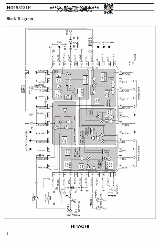
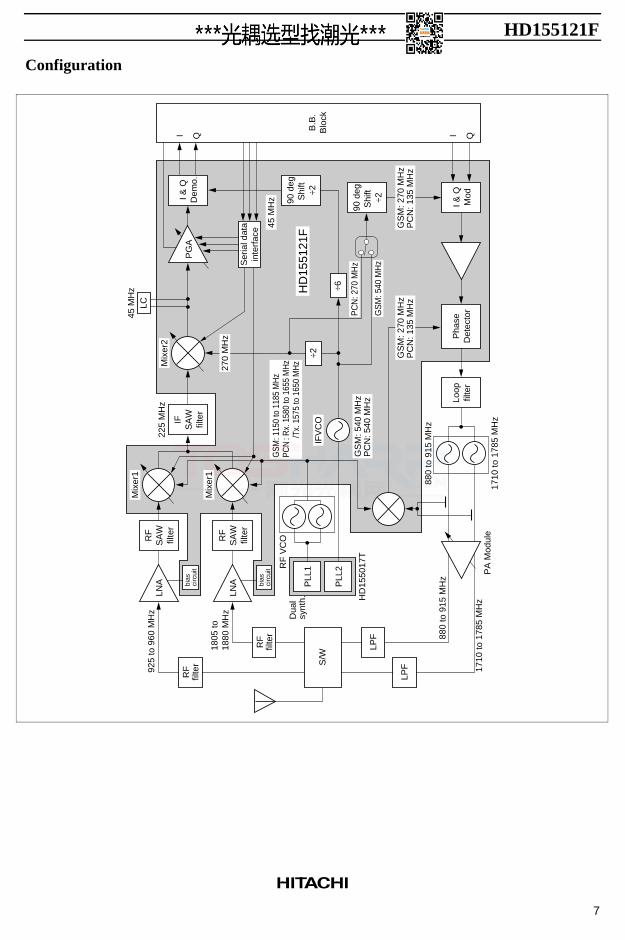
Block Diagram
1 12
36 35 34 33 32 31 30 29 28 27 26 25
1314
1516
1718
1920
2122
24
48
from
Sys
tem
con
trol
ler
(180
5MH
z)
(180
5MH
z)
(171
0MH
z) Tx.V
CO1
Tx.V
CO2
1172MHz(Rx: 1580MHz, Tx: 1575MHz)
from
VC
O
4746
4544
4342
4140
3938
37
23
MIX1IN2 QINB
QIN
IINB
IIN
MODB
VCCIQ
GNDIQ
QOUTB
QOUT
IOUTB
IOUT
MIX2OB
MIX1INB2
POONTX
POONRX2
POONRX1
MIX1OUTB
VCCMIX1
VCCDIV
RFLOIN
MIX1OUT
GNDMIX1
GNDDIV
MIX
1IN
B1
MIX
1IN
1
RF
OU
T
RF
IN1
RF
IN2
VC
CP
LL
GN
DP
LL
VC
OIN
2
VC
OIN
1
VC
CC
OM
P
PLL
OU
T
ICU
RA
D
IFLO
BA
ND
IFV
CO
O
IFV
CO
I
VC
CIF
GN
DIF
IFIN
IFIN
B
from System controllerfromSystem controller
LE SD
AT
A
CLK
MIX
2O
RIC
UR
AD
947M
Hz
947M
Hz
902M
Hz
45M
Hz
225M
Hz
(225
MH
z)
270M
Hz
(135
MH
z)
45M
Hz
(45M
Hz)
270M
Hz
(135
MH
z)
45M
Hz
(45M
Hz)
540
MHz
1172
MH
z(1
580/
1575
MH
z)
(158
0/15
75M
Hz)
1172
MH
z
GS
M: 2
70M
Hz
PC
N: 1
35M
Hz
225M
Hz
(225
MH
z)
Tun
e
to B
ase
band
from
Bas
e ba
nd
from Antenna
Cur
rent
mod
edr
iver
LNA
Bia
sci
rcui
t
2 3 4 5 6 7 8 9 10 11
Vre
f(P
LL)
Ser
ial
inte
rfac
e
1/2
(90d
eg)
from
Band
SW
Vre
f(D
iv.R
x)(D
iv.T
x)
1/2
(90d
eg)
Vre
f(L
NA
)
Vre
f(P
GA
)
Vre
f(I
F)
Vref
(IFVC
O)
Vre
f(M
od)
Vre
f(M
ix1)
Vre
f(D
emod
)
1/2
1/6
HD155121F
7
Configuration
LNA
HD
1550
17T
LPF
LPF
RF
filte
r
RF
filte
r
PA
Mod
ule
1710
to 1
785
MH
z
1710
to 1
785
MH
z
925
to 9
60 M
Hz
880
to 9
15 M
Hz
880
to 9
15 M
Hz
1805
to18
80 M
Hz
Loop
filte
rP
hase
Det
ecto
r
Ser
ial d
ata
inte
rfac
e
IFV
CO
GS
M: 5
40 M
Hz
PC
N: 5
40 M
Hz
GS
M: 2
70 M
Hz
PC
N: 1
35 M
Hz
GS
M: 2
70 M
Hz
PC
N: 1
35 M
Hz
HD
1551
21F
45 M
Hz
45 M
Hz
LC
IFS
AW
filte
r
RF
SA
Wfil
ter
LNA
RF
SA
Wfil
ter
225
MH
z
I & Q
Dem
o.
I & Q
Mod
I QI
B.B
.B
lock
Q
90 d
egS
hift
÷2
90 d
egS
hift
÷2
RF
VC
O
PLL
2
S/W
PLL
1
Dua
lsy
nth.
bias
circ
uit
bias
circ
uit
PG
A
Mix
er1
Mix
er2
Mix
er1
GSM
PCN
: 115
0 to
118
5 M
Hz
: Rx.
158
0 to
165
5 M
Hz
/Tx.
157
5 to
165
0 M
Hz
÷2
÷6
270
MH
z
PC
N: 2
70 M
Hz
GS
M: 5
40 M
Hz
HD155121F
8
Functional Operation
The HD155121F has been designed from system stand point and incorporated a large number of the circuitblocks necessary in the design of a digital cellular handset.
Receiver Operation
The HD155121F incorporates two LNA bias circuits for external RF transistors, whose NF and power gaincan be better selected.
This circuit amplifies the RF signal after selection by the antenna filter before the signal enters the firstmixer section. The RF signal is combined with a local oscillator (LO) signal to generate a wanted first IFsignal in the 130 - 300 MHz range. The first mixer circuit uses a double-balanced Gilbert cell architecture,which has open collector differential outputs. If, at 225 MHz, a 800 Ω LC load is connected to the mixer’soutputs then a SSB NF of 9.0 dB (GSM), 9.1 dB (PCN) with a gain of 9.5 dB (GSM), 8.5 dB (PCN) isrealizable. The corresponding input compression point is –10.5 dBm (GSM), –12.5 dBm (PCN), whichallows the device to be used within a GSM and EGSM and PCN system.
A filter is used after the first mixer to provide image rejection and the conditioned signal is then passedthrough an intermediate amplifier, before being down converted to a second IF in the range of 26 - 60MHz.
The second mixer can generate a 45 MHz second IF, if a 270 MHz second local signal is used. The secondmixer also uses the Gilbert cell architecture, but with internal resistive differential outputs of 300 Ω. Ifamplifier and second mixer has a SSB NF of 6.0 dB, a power gain of 13 dB and a input compression pointof –22 dBm. In order to improve the blocking characteristics of the device an external LC resonator acrossthe differential outputs of the second mixer is recommended.
First mixer and second mixer can switch the power gain. Switching gain step of first mixer is 12 dB, andsuch step of second mixer is 16 dB.
The signal is then passed to the PGA circuit, which has a dynamic range of more than 80 dB (–42 dB - +56dB typ.) and is controlled by digital serial data, which is generated by the microprocessor. This gain step is2 dB.
The signal is then down converted by a demodulator to I and Q. Internal divider circuits convert the IFLOsignal to the same frequency as the second IF before passing this local signal through a phase splitter /shifter in order to generate the in phase and quadrature phase IQ components. The phase accuracy of theIQ demodulator is less than +/–1 degree and the amplitude mismatch is less than +/–0.5 dB. In order toaccommodate different baseband interfaces the HD155121F IQ differential outputs have a voltage swing of1.6 Vpp and DC offset of less than +/–60 mV. Within each output stage a second order Butterworth filter(fc = 210 kHz) is used to improve the blocking performance of the device.
In order to allow flexibility in circuit implementation the HD155121F can configured to use either a single-ended or balanced external circuitry and components.
HD155121F
9
Transmitter Operation
The transmitter chain converts differential IQ baseband signals to a suitable format for transmission by apower amplifier.
The common mode voltage range of the modulator inputs is 0.8 V to 1.2 V and they have 2.0 Vppdifferential swing. The modulator circuit uses double-balanced mixers for the I and Q paths. The Localsignals are generated by dividing the IFLO signals by 2, and then passed to the modulator through a phasesplitter / shifter. The IF signals generated are then summed to produce a single modulated IF signal whichis amplified and fed into the offset PLL block. Carrier suppression due to the mixer circuit is better than 31dBc. If the common mode DC voltage of the I and Q inputs is adjusted, carrier suppression is better than40 dBc easily. Side band suppression is better than 35 dBc without adjustment.
Within the offset PLL block there are a down converter, a phase comparator and a VCO driver. The downconverter mixes the first local signal and the TXVCO signal to create a reference local signal for use in theoffset PLL circuit. The phase comparator and the VCO driver generate an error current, which isproportional to the phase differential between the reference IF and the modulated IF signals. This current isused in a second order loop filter to generate a voltage, which in turn modulates the TXVCO. In order tooptimize the PLL loop gain, the error current value can be modified by changing the value of an externalresistor - ICURAD. In order to accommodate various control range of TXVCOs, the offset PLL circuit hasbeen designed to operate with a supply voltage up to 5.25 V.
HD155121F
10
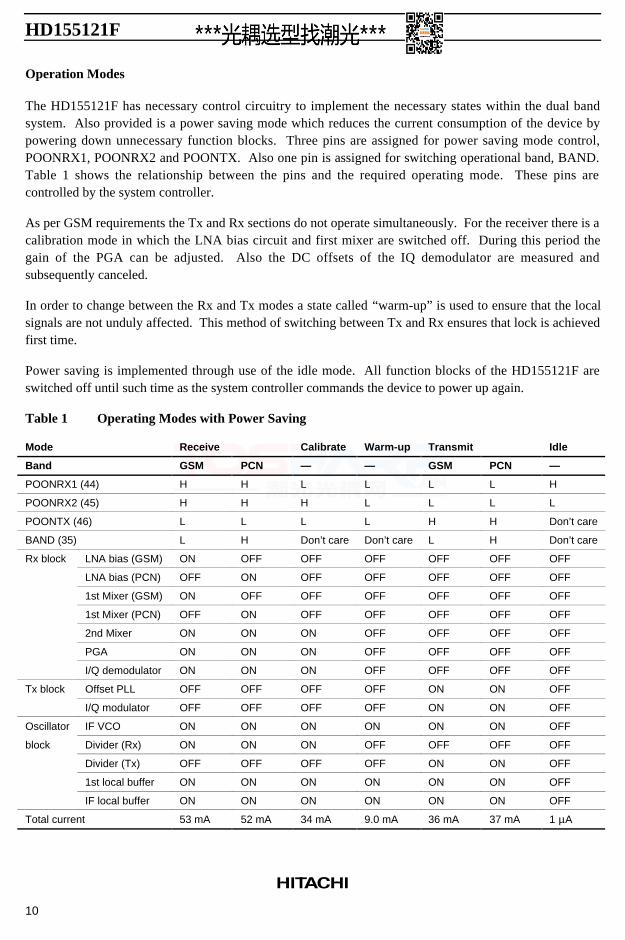
Operation Modes
The HD155121F has necessary control circuitry to implement the necessary states within the dual bandsystem. Also provided is a power saving mode which reduces the current consumption of the device bypowering down unnecessary function blocks. Three pins are assigned for power saving mode control,POONRX1, POONRX2 and POONTX. Also one pin is assigned for switching operational band, BAND.Table 1 shows the relationship between the pins and the required operating mode. These pins arecontrolled by the system controller.
As per GSM requirements the Tx and Rx sections do not operate simultaneously. For the receiver there is acalibration mode in which the LNA bias circuit and first mixer are switched off. During this period thegain of the PGA can be adjusted. Also the DC offsets of the IQ demodulator are measured andsubsequently canceled.
In order to change between the Rx and Tx modes a state called “warm-up” is used to ensure that the localsignals are not unduly affected. This method of switching between Tx and Rx ensures that lock is achievedfirst time.
Power saving is implemented through use of the idle mode. All function blocks of the HD155121F areswitched off until such time as the system controller commands the device to power up again.
Table 1 Operating Modes with Power Saving
Mode Receive Calibrate Warm-up Transmit Idle
Band GSM PCN — — GSM PCN —
POONRX1 (44) H H L L L L H
POONRX2 (45) H H H L L L L
POONTX (46) L L L L H H Don’t care
BAND (35) L H Don’t care Don’t care L H Don’t care
Rx block LNA bias (GSM) ON OFF OFF OFF OFF OFF OFF
LNA bias (PCN) OFF ON OFF OFF OFF OFF OFF
1st Mixer (GSM) ON OFF OFF OFF OFF OFF OFF
1st Mixer (PCN) OFF ON OFF OFF OFF OFF OFF
2nd Mixer ON ON ON OFF OFF OFF OFF
PGA ON ON ON OFF OFF OFF OFF
I/Q demodulator ON ON ON OFF OFF OFF OFF
Tx block Offset PLL OFF OFF OFF OFF ON ON OFF
I/Q modulator OFF OFF OFF OFF ON ON OFF
Oscillator IF VCO ON ON ON ON ON ON OFF
block Divider (Rx) ON ON ON OFF OFF OFF OFF
Divider (Tx) OFF OFF OFF OFF ON ON OFF
1st local buffer ON ON ON ON ON ON OFF
IF local buffer ON ON ON ON ON ON OFF
Total current 53 mA 52 mA 34 mA 9.0 mA 36 mA 37 mA 1 µA
HD155121F
11
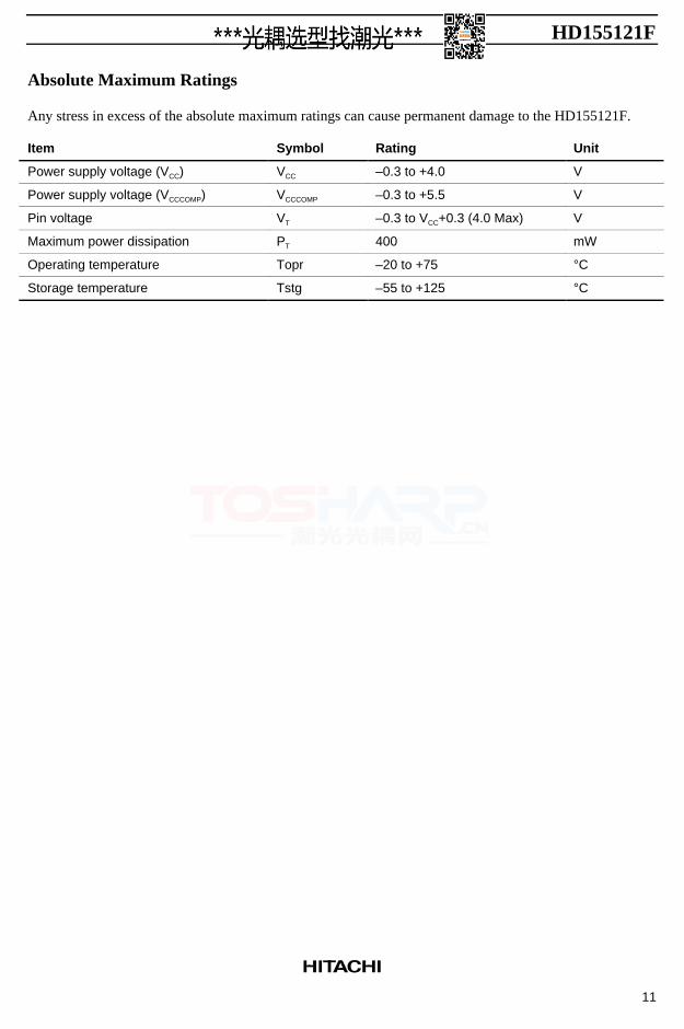
Absolute Maximum Ratings
Any stress in excess of the absolute maximum ratings can cause permanent damage to the HD155121F.
Item Symbol Rating Unit
Power supply voltage (VCC) VCC –0.3 to +4.0 V
Power supply voltage (VCCCOMP) VCCCOMP –0.3 to +5.5 V
Pin voltage VT –0.3 to VCC+0.3 (4.0 Max) V
Maximum power dissipation PT 400 mW
Operating temperature Topr –20 to +75 °C
Storage temperature Tstg –55 to +125 °C
HD155121F
12
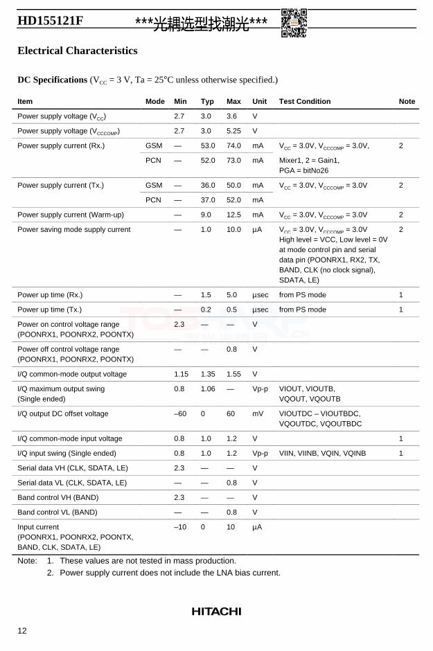
Electrical Characteristics
DC Specifications (VCC = 3 V, Ta = 25°C unless otherwise specified.)
Item Mode Min Typ Max Unit Test Condition Note
Power supply voltage (VCC) 2.7 3.0 3.6 V
Power supply voltage (VCCCOMP) 2.7 3.0 5.25 V
Power supply current (Rx.) GSM — 53.0 74.0 mA VCC = 3.0V, VCCCOMP = 3.0V, 2
PCN — 52.0 73.0 mA Mixer1, 2 = Gain1,PGA = bitNo26
Power supply current (Tx.) GSM — 36.0 50.0 mA VCC = 3.0V, VCCCOMP = 3.0V 2
PCN — 37.0 52.0 mA
Power supply current (Warm-up) — 9.0 12.5 mA VCC = 3.0V, VCCCOMP = 3.0V 2
Power saving mode supply current — 1.0 10.0 µA VCC = 3.0V, VCCCOMP = 3.0VHigh level = VCC, Low level = 0Vat mode control pin and serialdata pin (POONRX1, RX2, TX,BAND, CLK (no clock signal),SDATA, LE)
2
Power up time (Rx.) — 1.5 5.0 µsec from PS mode 1
Power up time (Tx.) — 0.2 0.5 µsec from PS mode 1
Power on control voltage range(POONRX1, POONRX2, POONTX)
2.3 — — V
Power off control voltage range(POONRX1, POONRX2, POONTX)
— — 0.8 V
I/Q common-mode output voltage 1.15 1.35 1.55 V
I/Q maximum output swing(Single ended)
0.8 1.06 — Vp-p VIOUT, VIOUTB,VQOUT, VQOUTB
I/Q output DC offset voltage –60 0 60 mV VIOUTDC – VIOUTBDC,VQOUTDC, VQOUTBDC
I/Q common-mode input voltage 0.8 1.0 1.2 V 1
I/Q input swing (Single ended) 0.8 1.0 1.2 Vp-p VIIN, VIINB, VQIN, VQINB 1
Serial data VH (CLK, SDATA, LE) 2.3 — — V
Serial data VL (CLK, SDATA, LE) — — 0.8 V
Band control VH (BAND) 2.3 — — V
Band control VL (BAND) — — 0.8 V
Input current(POONRX1, POONRX2, POONTX,BAND, CLK, SDATA, LE)
–10 0 10 µA
Note: 1. These values are not tested in mass production.2. Power supply current does not include the LNA bias current.
HD155121F
13
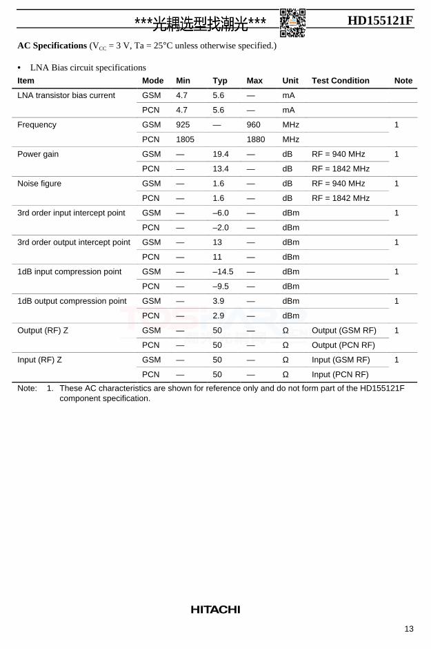
AC Specifications (VCC = 3 V, Ta = 25°C unless otherwise specified.)
• LNA Bias circuit specifications
Item Mode Min Typ Max Unit Test Condition Note
LNA transistor bias current GSM 4.7 5.6 — mA
PCN 4.7 5.6 — mA
Frequency GSM 925 — 960 MHz 1
PCN 1805 1880 MHz
Power gain GSM — 19.4 — dB RF = 940 MHz 1
PCN — 13.4 — dB RF = 1842 MHz
Noise figure GSM — 1.6 — dB RF = 940 MHz 1
PCN — 1.6 — dB RF = 1842 MHz
3rd order input intercept point GSM — –6.0 — dBm 1
PCN — –2.0 — dBm
3rd order output intercept point GSM — 13 — dBm 1
PCN — 11 — dBm
1dB input compression point GSM — –14.5 — dBm 1
PCN — –9.5 — dBm
1dB output compression point GSM — 3.9 — dBm 1
PCN — 2.9 — dBm
Output (RF) Z GSM — 50 — Ω Output (GSM RF) 1
PCN — 50 — Ω Output (PCN RF)
Input (RF) Z GSM — 50 — Ω Input (GSM RF) 1
PCN — 50 — Ω Input (PCN RF)
Note: 1. These AC characteristics are shown for reference only and do not form part of the HD155121Fcomponent specification.
HD155121F
14
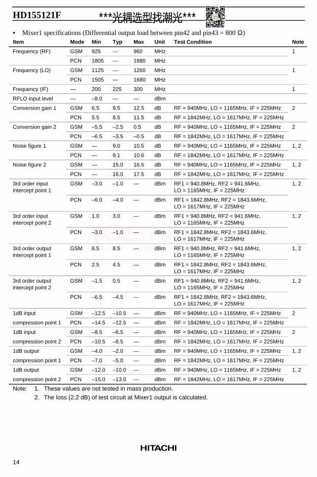
• Mixer1 specifications (Differential output load between pin42 and pin43 = 800 Ω)Item Mode Min Typ Max Unit Test Condition Note
Frequency (RF) GSM 925 — 960 MHz 1
PCN 1805 — 1880 MHz
Frequency (LO) GSM 1125 — 1260 MHz 1
PCN 1505 — 1680 MHz
Frequency (IF) — 200 225 300 MHz 1
RFLO input level — –8.0 — — dBm
Conversion gain 1 GSM 6.5 9.5 12.5 dB RF = 940MHz, LO = 1165MHz, IF = 225MHz 2
PCN 5.5 8.5 11.5 dB RF = 1842MHz, LO = 1617MHz, IF = 225MHz
Conversion gain 2 GSM –5.5 –2.5 0.5 dB RF = 940MHz, LO = 1165MHz, IF = 225MHz 2
PCN –6.5 –3.5 –0.5 dB RF = 1842MHz, LO = 1617MHz, IF = 225MHz
Noise figure 1 GSM — 9.0 10.5 dB RF = 940MHz, LO = 1165MHz, IF = 225MHz 1, 2
PCN — 9.1 10.6 dB RF = 1842MHz, LO = 1617MHz, IF = 225MHz
Noise figure 2 GSM — 15.0 16.5 dB RF = 940MHz, LO = 1165MHz, IF = 225MHz 1, 2
PCN — 16.0 17.5 dB RF = 1842MHz, LO = 1617MHz, IF = 225MHz
3rd order inputintercept point 1
GSM –3.0 –1.0 — dBm RF1 = 940.8MHz, RF2 = 941.6MHz,LO = 1165MHz, IF = 225MHz
1, 2
PCN –6.0 –4.0 — dBm RF1 = 1842.8MHz, RF2 = 1843.6MHz,LO = 1617MHz, IF = 225MHz
3rd order inputintercept point 2
GSM 1.0 3.0 — dBm RF1 = 940.8MHz, RF2 = 941.6MHz,LO = 1165MHz, IF = 225MHz
1, 2
PCN –3.0 –1.0 — dBm RF1 = 1842.8MHz, RF2 = 1843.6MHz,LO = 1617MHz, IF = 225MHz
3rd order outputintercept point 1
GSM 6.5 8.5 — dBm RF1 = 940.8MHz, RF2 = 941.6MHz,LO = 1165MHz, IF = 225MHz
1, 2
PCN 2.5 4.5 — dBm RF1 = 1842.8MHz, RF2 = 1843.6MHz,LO = 1617MHz, IF = 225MHz
3rd order outputintercept point 2
GSM –1.5 0.5 — dBm RF1 = 940.8MHz, RF2 = 941.6MHz,LO = 1165MHz, IF = 225MHz
1, 2
PCN –6.5 –4.5 — dBm RF1 = 1842.8MHz, RF2 = 1843.6MHz,LO = 1617MHz, IF = 225MHz
1dB input GSM –12.5 –10.5 — dBm RF = 940MHz, LO = 1165MHz, IF = 225MHz 2
compression point 1 PCN –14.5 –12.5 — dBm RF = 1842MHz, LO = 1617MHz, IF = 225MHz
1dB input GSM –8.5 –6.5 — dBm RF = 940MHz, LO = 1165MHz, IF = 225MHz 2
compression point 2 PCN –10.5 –8.5 — dBm RF = 1842MHz, LO = 1617MHz, IF = 225MHz
1dB output GSM –4.0 –2.0 — dBm RF = 940MHz, LO = 1165MHz, IF = 225MHz 1, 2
compression point 1 PCN –7.0 –5.0 — dBm RF = 1842MHz, LO = 1617MHz, IF = 225MHz
1dB output GSM –12.0 –10.0 — dBm RF = 940MHz, LO = 1165MHz, IF = 225MHz 1, 2
compression point 2 PCN –15.0 –13.0 — dBm RF = 1842MHz, LO = 1617MHz, IF = 225MHz
Note: 1. These values are not tested in mass production.2. The loss (2.2 dB) of test circuit at Mixer1 output is calculated.
HD155121F
15
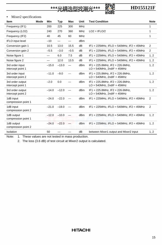
• Mixer2 specificationsItem Mode Min Typ Max Unit Test Condition Note
Frequency (IF1) 200 225 300 MHz 1
Frequency (LO2) 240 270 360 MHz LO2 = IFLO/2 1
Frequency (IF2) 40 45 60 MHz 1
IFLO input level –10 — — dBm
Conversion gain 1 10.5 13.0 15.5 dB IF1 = 225MHz, IFLO = 540MHz, IF2 = 45MHz 2
Conversion gain 2 –5.5 –3.0 –0.5 dB IF1 = 225MHz, IFLO = 540MHz, IF2 = 45MHz 2
Noise figure 1 — 6.0 7.5 dB IF1 = 225MHz, IFLO = 540MHz, IF2 = 45MHz 1, 2
Noise figure 2 — 12.0 13.5 dB IF1 = 225MHz, IFLO = 540MHz, IF2 = 45MHz 1, 2
3rd order inputintercept point 1
–15.0 –13.0 — dBm IF1 = 225.8MHz, IF2 = 226.6MHz,LO = 540MHz, 2ndIF = 45MHz
1, 2
3rd order inputintercept point 2
–11.0 –9.0 — dBm IF1 = 225.8MHz, IF2 = 226.6MHz,LO = 540MHz, 2ndIF = 45MHz
1, 2
3rd order outputintercept point 1
–2.0 0.0 — dBm IF1 = 225.8MHz, IF2 = 226.6MHz,LO = 540MHz, 2ndIF = 45MHz
1, 2
3rd order outputintercept point 2
–14.0 –12.0 — dBm IF1 = 225.8MHz, IF2 = 226.6MHz,LO = 540MHz, 2ndIF = 45MHz
1, 2
1dB inputcompression point 1
–24.0 –22.0 — dBm IF1 = 225MHz, IFLO = 540MHz, IF2 = 45MHz 2
1dB inputcompression point 2
–21.0 –19.0 — dBm IF1 = 225MHz, IFLO = 540MHz, IF2 = 45MHz 2
1dB outputcompression point 1
–12.0 –10.0 — dBm IF1 = 225MHz, IFLO = 540MHz, IF2 = 45MHz 1, 2
1dB outputcompression point 2
–24.0 –22.0 — dBm IF1 = 225MHz, IFLO = 540MHz, IF2 = 45MHz 1, 2
Isolation 50 — — dB between Mixer1 output and Mixer2 input 1, 2
Note: 1. These values are not tested in mass production.2. The loss (3.6 dB) of test circuit at Mixer2 output is calculated.
HD155121F
16
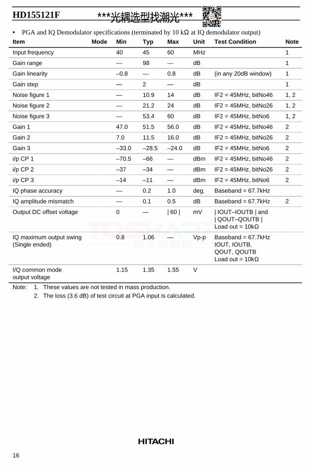
• PGA and IQ Demodulator specifications (terminated by 10 kΩ at IQ demodulator output)
Item Mode Min Typ Max Unit Test Condition Note
Input frequency 40 45 60 MHz 1
Gain range — 98 — dB 1
Gain linearity –0.8 — 0.8 dB (in any 20dB window) 1
Gain step — 2 — dB 1
Noise figure 1 — 10.9 14 dB IF2 = 45MHz, bitNo46 1, 2
Noise figure 2 — 21.2 24 dB IF2 = 45MHz, bitNo26 1, 2
Noise figure 3 — 53.4 60 dB IF2 = 45MHz, bitNo6 1, 2
Gain 1 47.0 51.5 56.0 dB IF2 = 45MHz, bitNo46 2
Gain 2 7.0 11.5 16.0 dB IF2 = 45MHz, bitNo26 2
Gain 3 –33.0 –28.5 –24.0 dB IF2 = 45MHz, bitNo6 2
i/p CP 1 –70.5 –66 — dBm IF2 = 45MHz, bitNo46 2
i/p CP 2 –37 –34 — dBm IF2 = 45MHz, bitNo26 2
i/p CP 3 –14 –11 — dBm IF2 = 45MHz, bitNo6 2
IQ phase accuracy — 0.2 1.0 deg. Baseband = 67.7kHz
IQ amplitude mismatch — 0.1 0.5 dB Baseband = 67.7kHz 2
Output DC offset voltage 0 — | 60 | mV | IOUT–IOUTB | and| QOUT–QOUTB |Load out = 10kΩ
IQ maximum output swing(Single ended)
0.8 1.06 — Vp-p Baseband = 67.7kHzIOUT, IOUTB,QOUT, QOUTBLoad out = 10kΩ
I/Q common modeoutput voltage
1.15 1.35 1.55 V
Note: 1. These values are not tested in mass production.2. The loss (3.6 dB) of test circuit at PGA input is calculated.
HD155121F
17
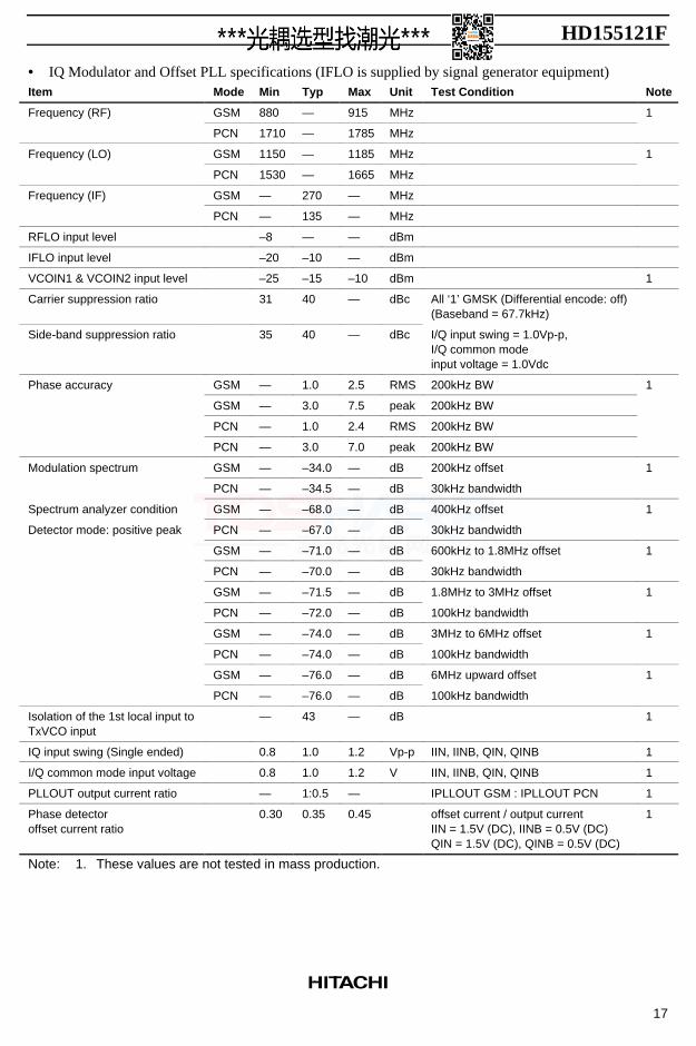
• IQ Modulator and Offset PLL specifications (IFLO is supplied by signal generator equipment)Item Mode Min Typ Max Unit Test Condition Note
Frequency (RF) GSM 880 — 915 MHz 1
PCN 1710 — 1785 MHz
Frequency (LO) GSM 1150 — 1185 MHz 1
PCN 1530 — 1665 MHz
Frequency (IF) GSM — 270 — MHz
PCN — 135 — MHz
RFLO input level –8 — — dBm
IFLO input level –20 –10 — dBm
VCOIN1 & VCOIN2 input level –25 –15 –10 dBm 1
Carrier suppression ratio 31 40 — dBc All ‘1’ GMSK (Differential encode: off)(Baseband = 67.7kHz)
Side-band suppression ratio 35 40 — dBc I/Q input swing = 1.0Vp-p,I/Q common modeinput voltage = 1.0Vdc
Phase accuracy GSM — 1.0 2.5 RMS 200kHz BW 1
GSM — 3.0 7.5 peak 200kHz BW
PCN — 1.0 2.4 RMS 200kHz BW
PCN — 3.0 7.0 peak 200kHz BW
Modulation spectrum GSM — –34.0 — dB 200kHz offset 1
PCN — –34.5 — dB 30kHz bandwidth
Spectrum analyzer condition GSM — –68.0 — dB 400kHz offset 1
Detector mode: positive peak PCN — –67.0 — dB 30kHz bandwidth
GSM — –71.0 — dB 600kHz to 1.8MHz offset 1
PCN — –70.0 — dB 30kHz bandwidth
GSM — –71.5 — dB 1.8MHz to 3MHz offset 1
PCN — –72.0 — dB 100kHz bandwidth
GSM — –74.0 — dB 3MHz to 6MHz offset 1
PCN — –74.0 — dB 100kHz bandwidth
GSM — –76.0 — dB 6MHz upward offset 1
PCN — –76.0 — dB 100kHz bandwidth
Isolation of the 1st local input toTxVCO input
— 43 — dB 1
IQ input swing (Single ended) 0.8 1.0 1.2 Vp-p IIN, IINB, QIN, QINB 1
I/Q common mode input voltage 0.8 1.0 1.2 V IIN, IINB, QIN, QINB 1
PLLOUT output current ratio — 1:0.5 — IPLLOUT GSM : IPLLOUT PCN 1
Phase detectoroffset current ratio
0.30 0.35 0.45 offset current / output currentIIN = 1.5V (DC), IINB = 0.5V (DC)QIN = 1.5V (DC), QINB = 0.5V (DC)
1
Note: 1. These values are not tested in mass production.
HD155121F
18
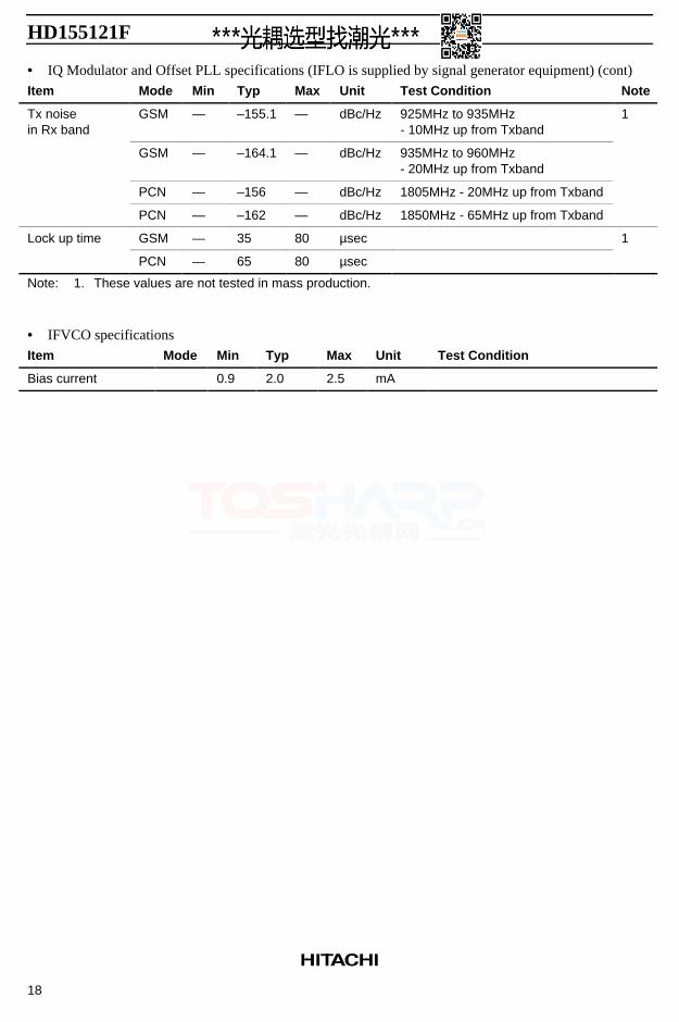
• IQ Modulator and Offset PLL specifications (IFLO is supplied by signal generator equipment) (cont)
Item Mode Min Typ Max Unit Test Condition Note
Tx noisein Rx band
GSM — –155.1 — dBc/Hz 925MHz to 935MHz- 10MHz up from Txband
1
GSM — –164.1 — dBc/Hz 935MHz to 960MHz- 20MHz up from Txband
PCN — –156 — dBc/Hz 1805MHz - 20MHz up from Txband
PCN — –162 — dBc/Hz 1850MHz - 65MHz up from Txband
Lock up time GSM — 35 80 µsec 1
PCN — 65 80 µsec
Note: 1. These values are not tested in mass production.
• IFVCO specifications
Item Mode Min Typ Max Unit Test Condition
Bias current 0.9 2.0 2.5 mA
HD155121F
19
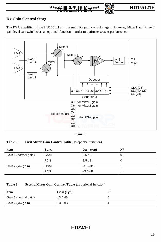
Rx Gain Control Stage
The PGA amplifier of the HD155121F is the main Rx gain control stage. However, Mixer1 and Mixer2gain level can switched as an optional function in order to optimize system performance.
biascircuit
LNA
Mixer1
Mixer2
biascircuit
LNA
Mixer1
X7
X7 : for Mixer1 gainX6 : for Mixer2 gainX5 :X4 :X3 :X2 :X1 :X0 :
Bit allocationfor PGA gain
X6 X5 X4 X3 X2 X1 X0
Decoder
Serial data
CLK (26)
IQ
SDATA (27)LE (28)
PGA I&QDemo.
Figure 1
Table 2 First Mixer Gain Control Table (as optional function)
Item Band Gain (typ) X7
Gain 1 (normal gain) GSM 9.5 dB 0
PCN 8.5 dB 0
Gain 2 (low gain) GSM –2.5 dB 1
PCN –3.5 dB 1
Table 3 Second Mixer Gain Control Table (as optional function)
Item Gain (Typ) X6
Gain 1 (normal gain) 13.0 dB 0
Gain 2 (low gain) –3.0 dB 1
HD155121F
20
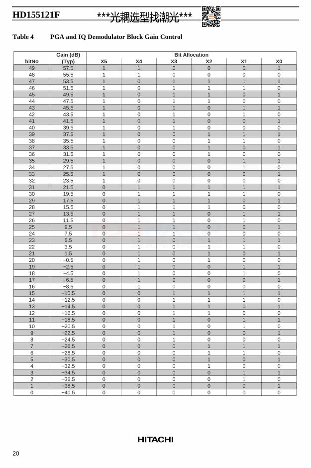
Table 4 PGA and IQ Demodulator Block Gain Control
bitNo494847464544434241403938373635343332313029282726252423222120191817161514131211109876543210
Gain (dB)(Typ)57.555.553.551.549.547.545.543.541.539.537.535.533.531.529.527.525.523.521.519.517.515.513.511.59.57.55.53.51.5
−0.5−2.5−4.5−6.5−8.5
−10.5−12.5−14.5−16.5−18.5−20.5−22.5−24.5−26.5−28.5−30.5−32.5−34.5−36.5−38.5−40.5
Bit AllocationX411000000000000000011111111111111110000000000000000
X300111111110000000011111111000000001111111100000000
X200111100001111000011110000111100001111000011110000
X100110011001100110011001100110011001100110011001100
X010101010101010101010101010101010101010101010101010
X511111111111111111100000000000000000000000000000000
HD155121F
21
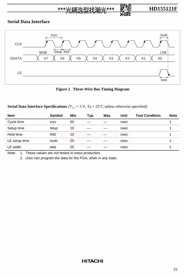
Serial Data Interface
tcyc
X6 X5 X4 X3 X2 X1 X0X7SDATA
CLK
LE
LSBMSB thldtstup
tsule
twle
Figure 2 Three-Wire Bus Timing Diagram
Serial Data Interface Specifications (VCC = 3 V, Ta = 25°C unless otherwise specified)
Item Symbol Min Typ Max Unit Test Condition Note
Cycle time tcyc 50 — — nsec 1
Setup time tstup 10 — — nsec 1
Hold time thld 10 — — nsec 1
LE setup time tsule 25 — — nsec 1
LE width twle 25 — — nsec 1
Note: 1. These values are not tested in mass production.2. User can program the data for the PGA, while in any state.
HD155121F
22
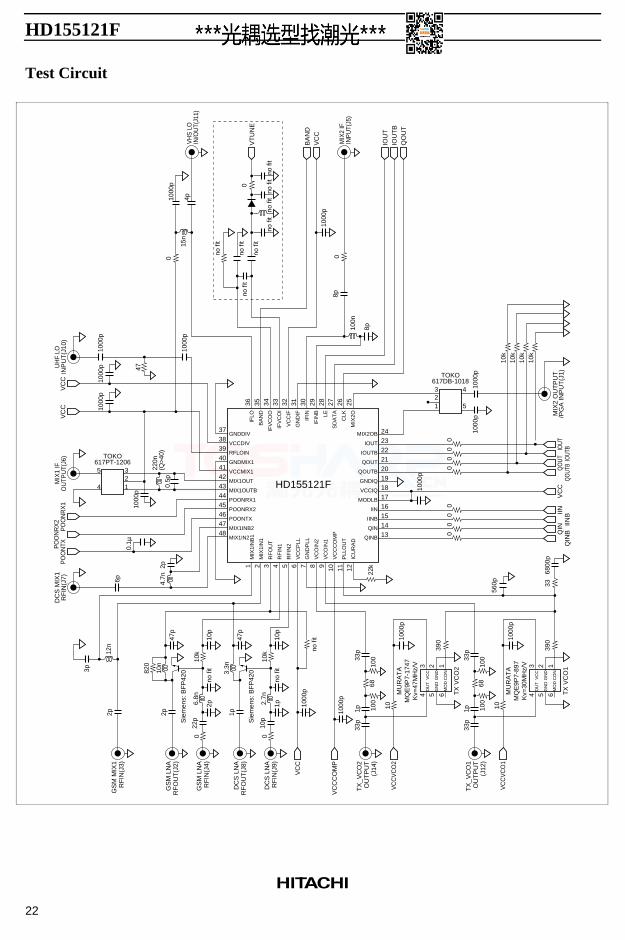
Test Circuit
VC
CV
CO
1
TX
_VC
O1
OU
TP
UT
(J12
)
MU
RA
TA
MQ
E9P
7-89
7K
v=30
MH
z/V
TX
VC
O1
4 5 6
3 2 1
QIN
B
IOU
TIO
UT
BQ
OU
T
VC
CB
AN
D
VT
UN
E
QIN
0
IINBIIN
VC
C
OU
TV
CC
GN
DG
ND
MO
DC
ON
390
1 2 3 4 5 6 7 8 9 10 11 12
36 35 34 33 32 31 30 29 28 27 26 25
373839404142434445464748
242322212019181716151413
MIX
1IN
B1
MIX
1IN
1
RF
OU
T
RF
IN1
RF
IN2
VC
CP
LL
GN
DP
LL
VC
OIN
2
VC
OIN
1
VC
CC
OM
P
PLL
OU
T
ICU
RA
D
MIX2OB
IOUT
IOUTB
QOUT
QOUTB
GNDIQ
VCCIQ
MODLB
IIN
IINB
QIN
QINB
GNDDIV
VCCDIV
RFLOIN
GNDMIX1
VCCMIX1
MIX1OUT
MIX1OUTB
POONRX1
POONRX2
POONTX
MIX1INB2
MIX1IN2
IFLO
BA
ND
IFV
CO
O
IFV
CO
I
VC
CIF
GN
DIF
IFIN
IFIN
B LE
SD
AT
A
CLK
MIX
2O
HD155121F
1000
p
33p
33p
1p
68
10
TX
_VC
O2
OU
TP
UT
(J14
)
GS
M M
IX1
RF
IN(J
3)
DC
S L
NA
RF
IN(J
9)
DC
S L
NA
RF
OU
T(J
8)
MIX
2 IF
INP
UT(
J5)
VH
S L
OIN
/OU
T(J1
1)
VC
CD
CS
MIX
1R
FIN
(J7)
100
8p
08p
100n
1000
p
1000
p10
00p
1000
p
no fi
tno
fit
no fi
t
no fi
t
no fi
t
VC
CC
OM
P10
00p
1000
p
1p
1000
p
1000
p47
1000
p
1000
p
6p
VC
C
47p
Sie
men
s: B
FP
420
10p
no fi
t
no fi
t
3.3n
1p
00
0
22k
QO
UTBQO
UT
0
IOUT
B
MIX
2 O
UT
PU
T/P
GA
INP
UT
(J1)
IOUT
00
0
2p4.
7n0.
5p(Q
>40)
220n
MIX
1 IF
OU
TPU
T(J6
)U
HF
LOIN
PU
T(J
10)
1000
p
VC
CP
OO
NR
X1
PO
ON
TXPO
ON
RX
2
1000
p
560p
0.1µ
3
TOKO617DB-1018
TOKO617PT-1206
21
4
5
321
5
4
10k
10k
10k
10k
0
0
no fi
t
no fi
t
no fi
t
15n
4p
3368
00p
10033
p33
p1p
6810
010
0
VC
CV
CO
2M
UR
AT
AM
QE
9P7-
1747
Kv=
47M
Hz/
V
TX
VC
O2
4 5 6
3 2 1
OU
TV
CC
GN
DG
ND
MO
DC
ON
39010
00p
10
010
k10
p2.
7n
GS
M L
NA
RF
IN(J
4)
GS
M L
NA
RF
OU
T(J
2)
2p
47p
Sie
men
s: B
FP
420
10p
no fi
t10n
2p2p12
n
010
k22
p6.
8n
820
3p
HD155121F
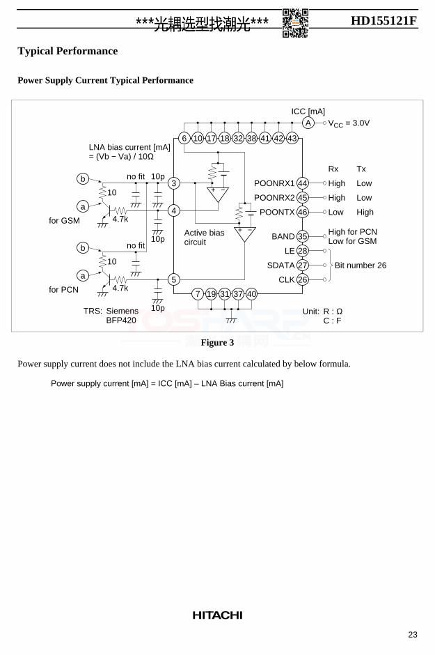
23
Typical Performance
Power Supply Current Typical Performance
6
310p
10p
10
4.7k
no fit
10 17 18 32 38
7 19 31 37 40
41 42 43
A VCC = 3.0VICC [mA]
−+
−+
10p
10
4.7k
no fit
Unit:TRS: SiemensBFP420
R : ΩC : F
4a
b
5 26
27 Bit number 26
28
35 High for PCNLow for GSM
High
for PCN
for GSM
CLK
SDATA
LE
BAND
46
45 High
Rx
Low
Low
Low
Tx
High
44
POONTX
POONRX2
POONRX1
Active biascircuit
LNA bias current [mA]= (Vb − Va) / 10Ω
a
b
Figure 3
Power supply current does not include the LNA bias current calculated by below formula.
Power supply current [mA] = ICC [mA] – LNA Bias current [mA]
HD155121F
24
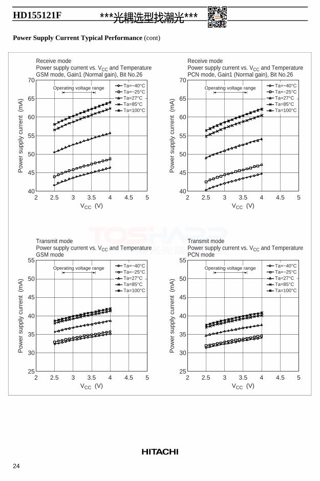
Power Supply Current Typical Performance (cont)
4054.543.5
VCC (V)32.52
54.543.5VCC (V)
32.52
45
50
55
60
65
70
Receive modePower supply current vs. VCC and TemperatureGSM mode, Gain1 (Normal gain), Bit No.26
Pow
er s
uppl
y cu
rren
t (m
A)
25
30
35
40
45
50
55
Transmit modePower supply current vs. VCC and TemperatureGSM mode
Transmit modePower supply current vs. VCC and TemperaturePCN mode
Pow
er s
uppl
y cu
rren
t (m
A)
54.543.5VCC (V)
32.5225
30
35
40
45
50
55
Pow
er s
uppl
y cu
rren
t (m
A)
4054.543.5
VCC (V)32.52
45
50
55
60
65
70
Receive modePower supply current vs. VCC and TemperaturePCN mode, Gain1 (Normal gain), Bit No.26
Pow
er s
uppl
y cu
rren
t (m
A)
Operating voltage range Ta=−40°C
Ta=100°CTa=85°CTa=27°CTa=−25°C
Ta=−40°C
Ta=100°CTa=85°CTa=27°CTa=−25°C
Ta=−40°C
Ta=100°CTa=85°CTa=27°CTa=−25°C
Ta=−40°C
Ta=100°CTa=85°CTa=27°CTa=−25°C
Operating voltage range
Operating voltage rangeOperating voltage range
HD155121F
25
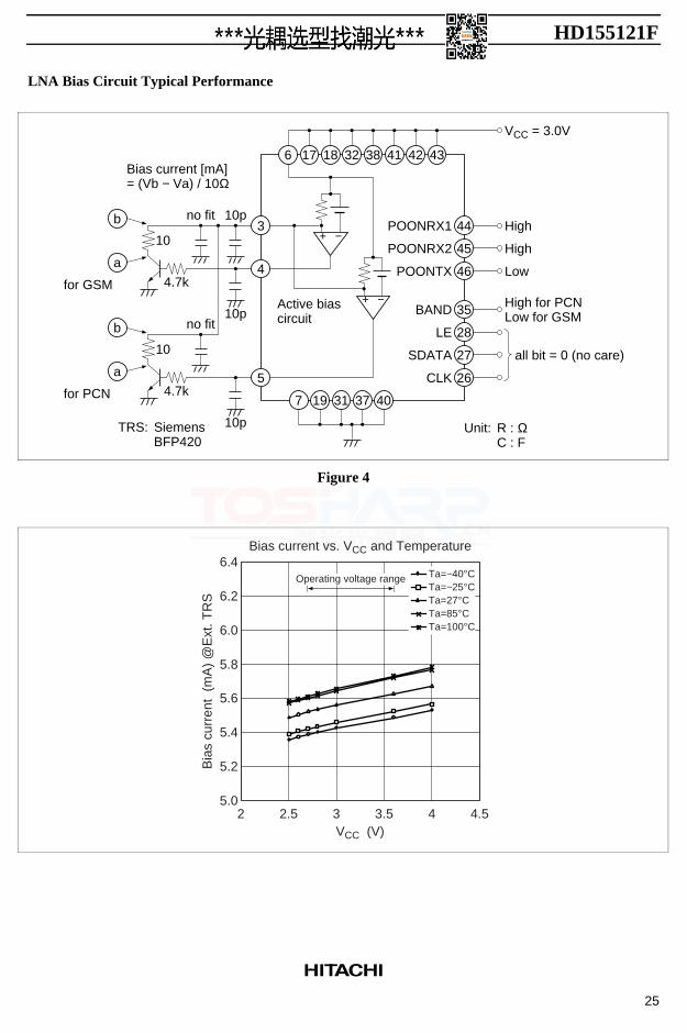
LNA Bias Circuit Typical Performance
310p
10p
10
4.7k
no fit
6 17 18 32 38
7 19 31 37 40
41 42 43
VCC = 3.0V
−+
−+
10p
10
4.7k
no fit
Unit:TRS: SiemensBFP420
R : ΩC : F
4a
b
5 26
27 all bit = 0 (no care)
28
35 High for PCNLow for GSM
High
for PCN
for GSM
CLK
SDATA
LE
BAND
46
45 High
Low
44
POONTX
POONRX2
POONRX1
Active biascircuit
Bias current [mA]= (Vb − Va) / 10Ω
a
b
Figure 4
4.543.5VCC (V)32.52
Bias current vs. VCC and Temperature
5.0
5.2
5.4
5.6
5.8
6.0
6.2
6.4
Bia
s cu
rren
t (m
A)
@E
xt. T
RS
Ta=−40°C
Ta=100°CTa=85°CTa=27°CTa=−25°C
Operating voltage range
HD155121F
26
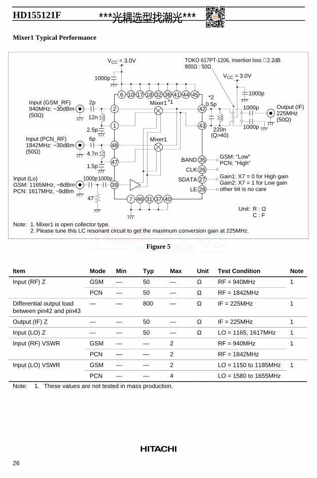
Mixer1 Typical Performance
6
2
1 43
42
1000p
2.5p
12n
10 17 18 32 38
7 46 31 37 40
41 44 45
VCC = 3.0V
Mixer12p 0.5p*2
*1
220n(Q>40)
Unit: R : ΩC : F
28
27
26
35 GSM: "Low"PCN: "High"
Gain1: X7 = 0 for High gainGain2: X7 = 1 for Low gainother bit is no care
Input (GSM_RF)940MHz: −30dBm(50Ω)
Output (IF)225MHz(50Ω)
LE
SDATA
CLK
BAND
1000p
1000p
1000p
VCC = 3.0V
TOKO 617PT-1206, insertion loss ≅ 2.2dB800Ω : 50Ω
48
471.5p
4.7n
47
Mixer16pInput (PCN_RF)1842MHz: −30dBm(50Ω)
Input (Lo)GSM: 1165MHz, −8dBmPCN: 1617MHz, −8dBm
Note: 1.2.
Mixer1 is open collector type.Please tune this LC resonant circuit to get the maximum conversion gain at 225MHz.
391000p1000p
Figure 5
Item Mode Min Typ Max Unit Test Condition Note
Input (RF) Z GSM — 50 — Ω RF = 940MHz 1
PCN — 50 — Ω RF = 1842MHz
Differential output loadbetween pin42 and pin43
— — 800 — Ω IF = 225MHz 1
Output (IF) Z — — 50 — Ω IF = 225MHz 1
Input (LO) Z — — 50 — Ω LO = 1165, 1617MHz 1
Input (RF) VSWR GSM — — 2 RF = 940MHz 1
PCN — — 2 RF = 1842MHz
Input (LO) VSWR GSM — — 2 LO = 1150 to 1185MHz 1
PCN — — 4 LO = 1580 to 1655MHz
Note: 1. These values are not tested in mass production.
HD155121F
27
Mixer1 Typical Performance (cont)
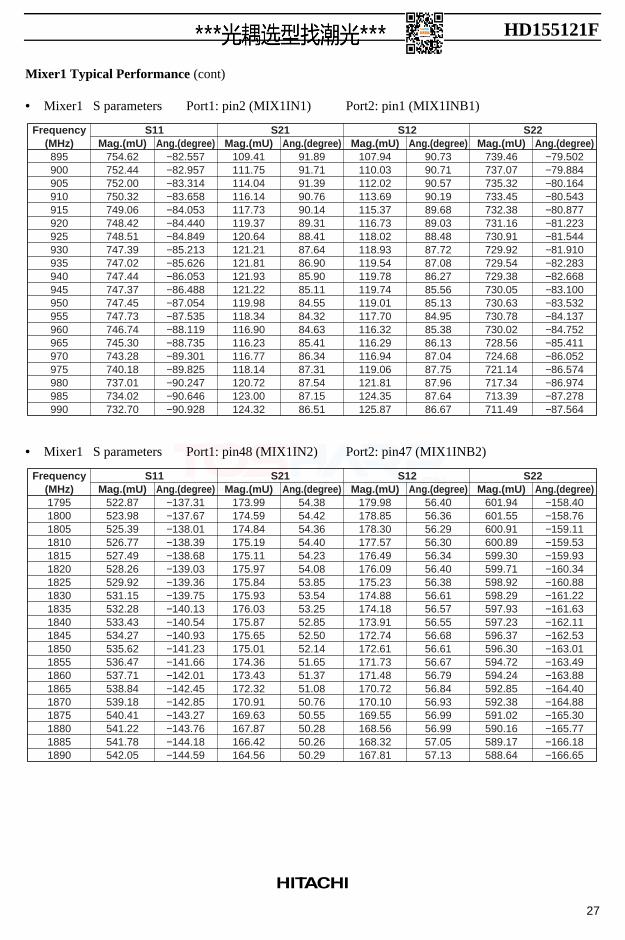
• Mixer1 S parameters Port1: pin2 (MIX1IN1) Port2: pin1 (MIX1INB1)
Frequency(MHz)895900905910915920925930935940945950955960965970975980985990
S21S11 S22S12Ang.(degree)
−82.557−82.957−83.314−83.658−84.053−84.440−84.849−85.213−85.626−86.053−86.488−87.054−87.535−88.119−88.735−89.301−89.825−90.247−90.646−90.928
Ang.(degree)91.8991.7191.3990.7690.1489.3188.4187.6486.9085.9085.1184.5584.3284.6385.4186.3487.3187.5487.1586.51
Ang.(degree)90.7390.7190.5790.1989.6889.0388.4887.7287.0886.2785.5685.1384.9585.3886.1387.0487.7587.9687.6486.67
Ang.(degree)−79.502−79.884−80.164−80.543−80.877−81.223−81.544−81.910−82.283−82.668−83.100−83.532−84.137−84.752−85.411−86.052−86.574−86.974−87.278−87.564
Mag.(mU)754.62752.44752.00750.32749.06748.42748.51747.39747.02747.44747.37747.45747.73746.74745.30743.28740.18737.01734.02732.70
Mag.(mU)109.41111.75114.04116.14117.73119.37120.64121.21121.81121.93121.22119.98118.34116.90116.23116.77118.14120.72123.00124.32
Mag.(mU)107.94110.03112.02113.69115.37116.73118.02118.93119.54119.78119.74119.01117.70116.32116.29116.94119.06121.81124.35125.87
Mag.(mU)739.46737.07735.32733.45732.38731.16730.91729.92729.54729.38730.05730.63730.78730.02728.56724.68721.14717.34713.39711.49
• Mixer1 S parameters Port1: pin48 (MIX1IN2) Port2: pin47 (MIX1INB2)
Frequency(MHz)17951800180518101815182018251830183518401845185018551860186518701875188018851890
S21S11 S22S12Ang.(degree)
−137.31−137.67−138.01−138.39−138.68−139.03−139.36−139.75−140.13−140.54−140.93−141.23−141.66−142.01−142.45−142.85−143.27−143.76−144.18−144.59
Ang.(degree)54.3854.4254.3654.4054.2354.0853.8553.5453.2552.8552.5052.1451.6551.3751.0850.7650.5550.2850.2650.29
Ang.(degree)56.4056.3656.2956.3056.3456.4056.3856.6156.5756.5556.6856.6156.6756.7956.8456.9356.9956.9957.0557.13
Ang.(degree)−158.40−158.76−159.11−159.53−159.93−160.34−160.88−161.22−161.63−162.11−162.53−163.01−163.49−163.88−164.40−164.88−165.30−165.77−166.18−166.65
Mag.(mU)522.87523.98525.39526.77527.49528.26529.92531.15532.28533.43534.27535.62536.47537.71538.84539.18540.41541.22541.78542.05
Mag.(mU)173.99174.59174.84175.19175.11175.97175.84175.93176.03175.87175.65175.01174.36173.43172.32170.91169.63167.87166.42164.56
Mag.(mU)179.98178.85178.30177.57176.49176.09175.23174.88174.18173.91172.74172.61171.73171.48170.72170.10169.55168.56168.32167.81
Mag.(mU)601.94601.55600.91600.89599.30599.71598.92598.29597.93597.23596.37596.30594.72594.24592.85592.38591.02590.16589.17588.64
HD155121F
28
Mixer1 Typical Performance (cont)
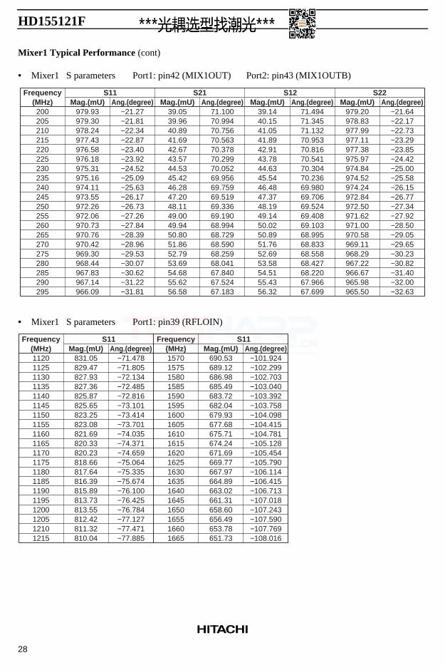
• Mixer1 S parameters Port1: pin42 (MIX1OUT) Port2: pin43 (MIX1OUTB)
Frequency(MHz)200205210215220225230235240245250255260265270275280285290295
S21S11 S22S12Ang.(degree)
−21.27−21.81−22.34−22.87−23.40−23.92−24.52−25.09−25.63−26.17−26.73−27.26−27.84−28.39−28.96−29.53−30.07−30.62−31.22−31.81
Ang.(degree)71.10070.99470.75670.56370.37870.29970.05269.95669.75969.51969.33669.19068.99468.72968.59068.25968.04167.84067.52467.183
Ang.(degree)71.49471.34571.13270.95370.81670.54170.30470.23669.98069.70669.52469.40869.10368.99568.83368.55868.42768.22067.96667.699
Ang.(degree)−21.64−22.17−22.73−23.29−23.85−24.42−25.00−25.58−26.15−26.77−27.34−27.92−28.50−29.05−29.65−30.23−30.82−31.40−32.00−32.63
Mag.(mU)979.93979.30978.24977.43976.58976.18975.31975.16974.11973.55972.26972.06970.73970.76970.42969.30968.44967.83967.14966.09
Mag.(mU)39.0539.9640.8941.6942.6743.5744.5345.4246.2847.2048.1149.0049.9450.8051.8652.7953.6954.6855.6256.58
Mag.(mU)39.1440.1541.0541.8942.9143.7844.6345.5446.4847.3748.1949.1450.0250.8951.7652.6953.5854.5155.4356.32
Mag.(mU)979.20978.83977.99977.11977.38975.97974.84974.52974.24972.84972.50971.62971.00970.58969.11968.29967.22966.67965.98965.50
• Mixer1 S parameters Port1: pin39 (RFLOIN)
Frequency(MHz)11201125113011351140114511501155116011651170117511801185119011951200120512101215
S11 S11Ang.(degree)
−71.478−71.805−72.134−72.485−72.816−73.101−73.414−73.701−74.035−74.371−74.659−75.064−75.335−75.674−76.100−76.425−76.784−77.127−77.471−77.885
Ang.(degree)−101.924−102.299−102.703−103.040−103.392−103.758−104.098−104.415−104.781−105.128−105.454−105.790−106.114−106.415−106.713−107.018−107.243−107.590−107.769−108.016
Mag.(mU)831.05829.47827.93827.36825.87825.65823.25823.08821.69820.33820.23818.66817.64816.39815.89813.73813.55812.42811.32810.04
Mag.(mU)690.53689.12686.98685.49683.72682.04679.93677.68675.71674.24671.69669.77667.97664.89663.02661.31658.60656.49653.78651.73
Frequency(MHz)15701575158015851590159516001605161016151620162516301635164016451650165516601665
HD155121F
29
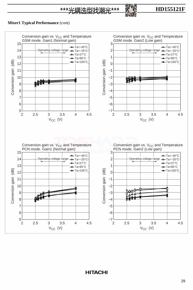
Mixer1 Typical Performance (cont)
4.543.5VCC (V)32.52
4.543.5VCC (V)32.52
Conversion gain vs. VCC and TemperatureGSM mode. Gain1 (Normal gain)
5
6
7
8
9
10
11
12
13
14
15
Con
vers
ion
gain
(dB
)
5
6
7
8
9
10
11
12
13
14
15
Con
vers
ion
gain
(dB
)
Operating voltage range
Conversion gain vs. VCC and TemperaturePCN mode. Gain1 (Normal gain)
Operating voltage range
Ta=−40°C
Ta=100°CTa=85°CTa=27°CTa=−25°C
4.543.5VCC (V)32.52
Conversion gain vs. VCC and TemperatureGSM mode. Gain2 (Low gain)
−7
−6
−5
−4
−3
−2
−1
0
1
2
3
Con
vers
ion
gain
(dB
)
Ta=−40°C
Ta=100°CTa=85°CTa=27°CTa=−25°COperating voltage range
4.543.5VCC (V)32.52
Conversion gain vs. VCC and TemperaturePCN mode. Gain2 (Low gain)
−7
−6
−5
−4
−3
−2
−1
0
1
2
3
Con
vers
ion
gain
(dB
)
Ta=−40°C
Ta=100°CTa=85°CTa=27°CTa=−25°COperating voltage range
Ta=−40°C
Ta=100°CTa=85°CTa=27°CTa=−25°C
HD155121F
30
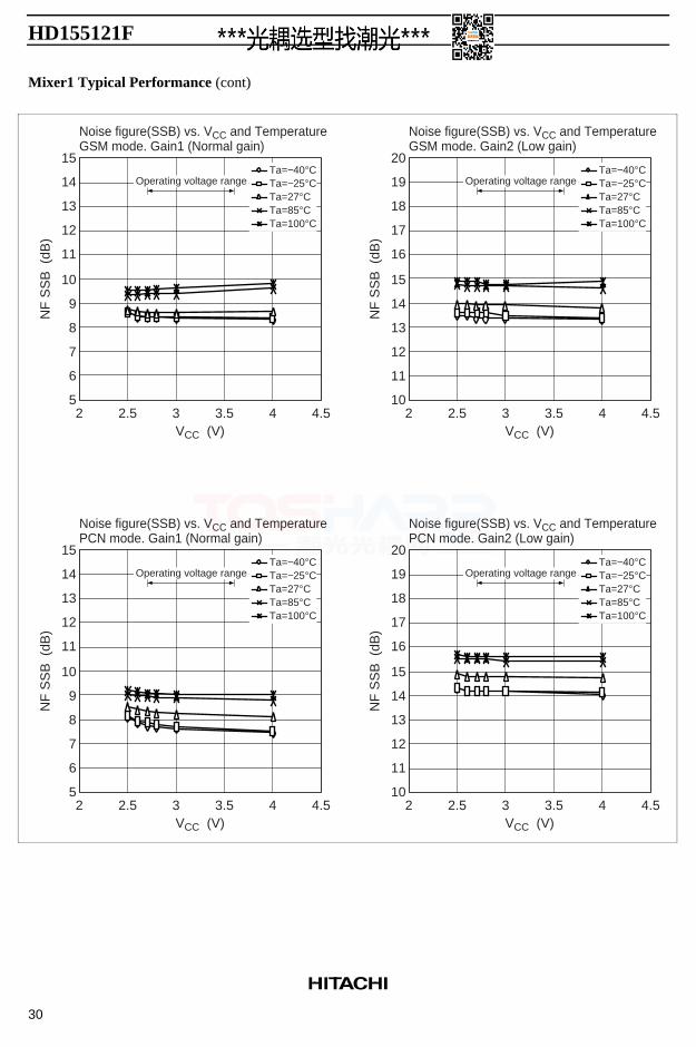
Mixer1 Typical Performance (cont)
4.543.5VCC (V)32.52
4.543.5VCC (V)32.52
Noise figure(SSB) vs. VCC and TemperatureGSM mode. Gain1 (Normal gain)
5
6
7
8
9
10
11
12
13
14
15
NF
SS
B (
dB)
5
6
7
8
9
10
11
12
13
14
15
NF
SS
B (
dB)
Operating voltage range
Noise figure(SSB) vs. VCC and TemperaturePCN mode. Gain1 (Normal gain)
Operating voltage range
Ta=−40°C
Ta=100°CTa=85°CTa=27°CTa=−25°C
4.543.5VCC (V)32.52
Noise figure(SSB) vs. VCC and TemperatureGSM mode. Gain2 (Low gain)
10
11
12
13
14
15
16
17
18
19
20
10
11
12
13
14
15
16
17
18
19
20
NF
SS
B (
dB)
Ta=−40°C
Ta=100°CTa=85°CTa=27°CTa=−25°COperating voltage range
4.543.5VCC (V)32.52
Noise figure(SSB) vs. VCC and TemperaturePCN mode. Gain2 (Low gain)
NF
SS
B (
dB)
Ta=−40°C
Ta=100°CTa=85°CTa=27°CTa=−25°COperating voltage range
Ta=−40°C
Ta=100°CTa=85°CTa=27°CTa=−25°C
HD155121F
31
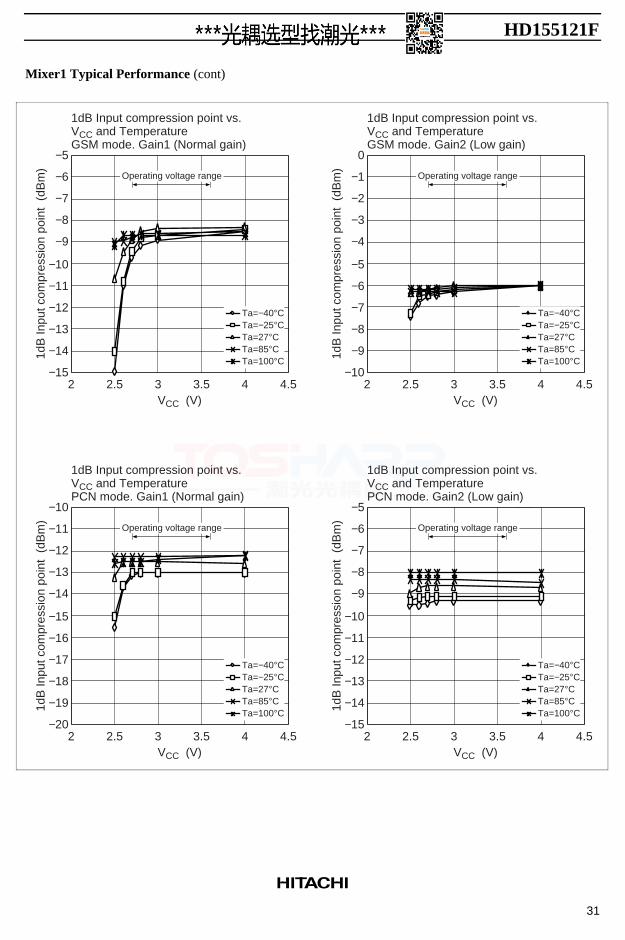
Mixer1 Typical Performance (cont)
4.543.5VCC (V)32.52
4.543.5VCC (V)32.52
1dB Input compression point vs.VCC and TemperatureGSM mode. Gain1 (Normal gain)
−15
−14
−13
−12
−11
−10
−9
−8
−7
−6
−5
1dB
Inpu
t com
pres
sion
poi
nt (
dBm
)
−20
−19
−18
−17
−16
−15
−14
−13
−12
−11
−10
1dB
Inpu
t com
pres
sion
poi
nt (
dBm
)
Operating voltage range
1dB Input compression point vs.VCC and TemperaturePCN mode. Gain1 (Normal gain)
Operating voltage range
Ta=−40°C
Ta=100°CTa=85°CTa=27°CTa=−25°C
4.543.5VCC (V)32.52
1dB Input compression point vs.VCC and TemperatureGSM mode. Gain2 (Low gain)
−10
−9
−8
−7
−6
−5
−4
−3
−2
−1
0
1dB
Inpu
t com
pres
sion
poi
nt (
dBm
)
Ta=−40°C
Ta=100°CTa=85°CTa=27°CTa=−25°C
Operating voltage range
4.543.5VCC (V)32.52
1dB Input compression point vs.VCC and TemperaturePCN mode. Gain2 (Low gain)
−15
−14
−13
−12
−11
−10
−9
−8
−7
−6
−5
1dB
Inpu
t com
pres
sion
poi
nt (
dBm
)
Ta=−40°C
Ta=100°CTa=85°CTa=27°CTa=−25°C
Operating voltage range
Ta=−40°C
Ta=100°CTa=85°CTa=27°CTa=−25°C
HD155121F
32
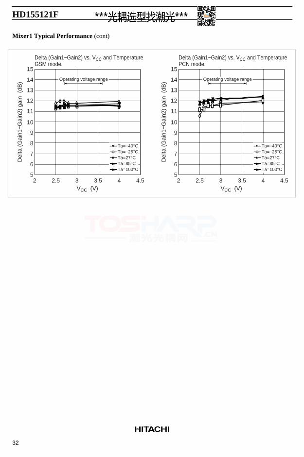
Mixer1 Typical Performance (cont)
4.543.5VCC (V)32.52
5
6
7
8
9
10
11
12
13
14
15
Del
ta (
Gai
n1−G
ain2
) ga
in (
dB)
5
6
7
8
9
10
11
12
13
14
15
Del
ta (
Gai
n1−G
ain2
) ga
in (
dB)
Delta (Gain1−Gain2) vs. VCC and TemperatureGSM mode.
Delta (Gain1−Gain2) vs. VCC and TemperaturePCN mode.
Operating voltage range
4.543.5VCC (V)32.52
Ta=−40°C
Ta=100°CTa=85°CTa=27°CTa=−25°C
Operating voltage range
Ta=−40°C
Ta=100°CTa=85°CTa=27°CTa=−25°C
HD155121F
33
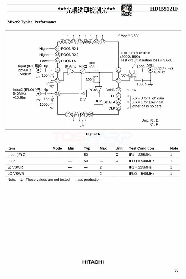
Mixer2 Typical Performance
Unit: R : ΩC : F
Output (IF2)45MHz
26
27
28
35 Low
X6 = 0 for High gainX6 = 1 for Low gainother bit is no care
CLK
SDATA
LE
BAND
VCC = 3.0V
TOKO 617DB1018(200Ω: 50Ω)Test circuit insertion loss = 3.6dB
6
30
298p
100n NC
17 18 32 38 41
7 19
IF Amp MIX2
PGA
300
300
31 37 40
42 43
8pInput (IF1)225MHz−50dBm
36
1000p
15n
4pInput2 (IFLO)540MHz−10dBm
High POONRX144
High POONRX245
Low POONTX46
25
241000p
1000p50Ω
50Ω
50Ω
÷2
DIV DEM
Figure 6
Item Mode Min Typ Max Unit Test Condition Note
Input (IF) Z — 50 — Ω IF1 = 225MHz 1
LO Z — 50 — Ω IFLO = 540MHz 1
i/p VSWR — — 2 IF1 = 225MHz 1
LO VSWR — — 2 IFLO = 540MHz 1
Note: 1. These values are not tested in mass production.
HD155121F
34
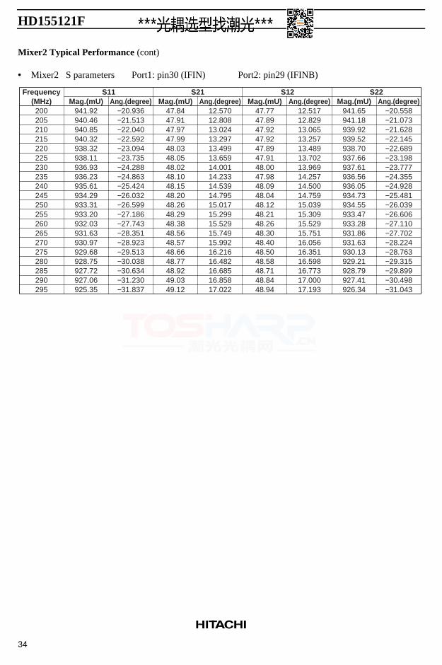
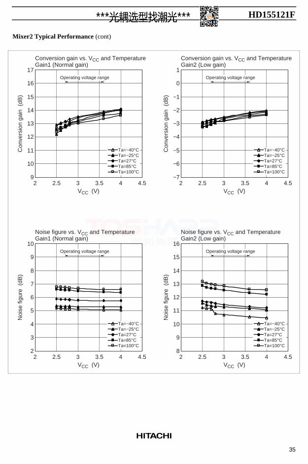
Mixer2 Typical Performance (cont)
• Mixer2 S parameters Port1: pin30 (IFIN) Port2: pin29 (IFINB)
Frequency(MHz)200205210215220225230235240245250255260265270275280285290295
S21S11 S22S12Ang.(degree)
−20.936−21.513−22.040−22.592−23.094−23.735−24.288−24.863−25.424−26.032−26.599−27.186−27.743−28.351−28.923−29.513−30.038−30.634−31.230−31.837
Ang.(degree)12.57012.80813.02413.29713.49913.65914.00114.23314.53914.79515.01715.29915.52915.74915.99216.21616.48216.68516.85817.022
Ang.(degree)12.51712.82913.06513.25713.48913.70213.96914.25714.50014.75915.03915.30915.52915.75116.05616.35116.59816.77317.00017.193
Ang.(degree)−20.558−21.073−21.628−22.145−22.689−23.198−23.777−24.355−24.928−25.481−26.039−26.606−27.110−27.702−28.224−28.763−29.315−29.899−30.498−31.043
Mag.(mU)941.92940.46940.85940.32938.32938.11936.93936.23935.61934.29933.31933.20932.03931.63930.97929.68928.75927.72927.06925.35
Mag.(mU)47.8447.9147.9747.9948.0348.0548.0248.1048.1548.2048.2648.2948.3848.5648.5748.6648.7748.9249.0349.12
Mag.(mU)47.7747.8947.9247.9247.8947.9148.0047.9848.0948.0448.1248.2148.2648.3048.4048.5048.5848.7148.8448.94
Mag.(mU)941.65941.18939.92939.52938.70937.66937.61936.56936.05934.73934.55933.47933.28931.86931.63930.13929.21928.79927.41926.34
HD155121F
35
Mixer2 Typical Performance (cont)
4.543.5VCC (V)32.52
4.543.5VCC (V)32.52
Conversion gain vs. VCC and TemperatureGain1 (Normal gain)
9
10
11
12
13
14
15
16
17
Con
vers
ion
gain
(dB
)N
oise
figu
re (
dB)
Operating voltage range
Noise figure vs. VCC and TemperatureGain1 (Normal gain)
Operating voltage range
4.543.5VCC (V)32.52
Conversion gain vs. VCC and TemperatureGain2 (Low gain)
Operating voltage range
4.543.5VCC (V)32.52
Noise figure vs. VCC and TemperatureGain2 (Low gain)
Noi
se fi
gure
(dB
)
Operating voltage range
2
3
4
5
6
7
8
9
10
8
9
10
11
12
13
14
15
16
−7
−6
−5
−4
−3
−2
−1
0
1
Con
vers
ion
gain
(dB
)
Ta=−40°C
Ta=100°CTa=85°CTa=27°CTa=−25°C
Ta=−40°C
Ta=100°CTa=85°CTa=27°CTa=−25°C
Ta=−40°C
Ta=100°CTa=85°CTa=27°CTa=−25°C
Ta=−40°C
Ta=100°CTa=85°CTa=27°CTa=−25°C
HD155121F
36
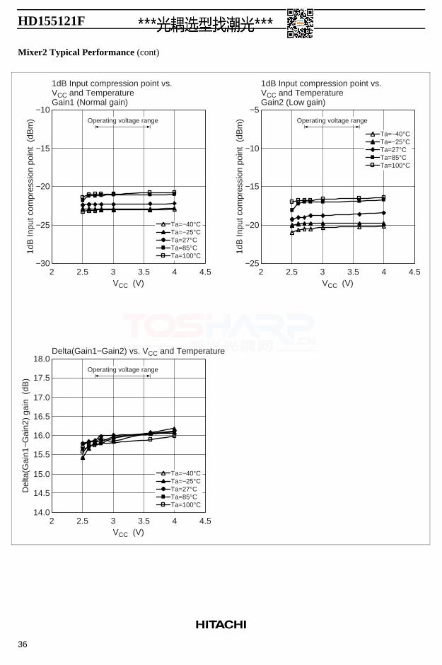
Mixer2 Typical Performance (cont)
4.543.5VCC (V)32.52
4.543.5VCC (V)32.52
1dB Input compression point vs.VCC and TemperatureGain1 (Normal gain)
1dB Input compression point vs.VCC and TemperatureGain2 (Low gain)
1dB
Inpu
t com
pres
sion
poi
nt (
dBm
)D
elta
(Gai
n1−G
ain2
) ga
in (
dB)
Delta(Gain1−Gain2) vs. VCC and Temperature
4.543.5VCC (V)32.52
1dB
Inpu
t com
pres
sion
poi
nt (
dBm
)
Ta=−40°C
Ta=100°CTa=85°CTa=27°CTa=−25°C
Operating voltage range
Ta=−40°C
Ta=100°CTa=85°CTa=27°CTa=−25°C
Operating voltage range
Ta=−40°C
Ta=100°CTa=85°CTa=27°CTa=−25°C
Operating voltage range
−30
−25
−20
−15
−10
14.0
14.5
15.0
15.5
16.0
16.5
17.0
17.5
18.0
−25
−20
−15
−10
−5
HD155121F
37
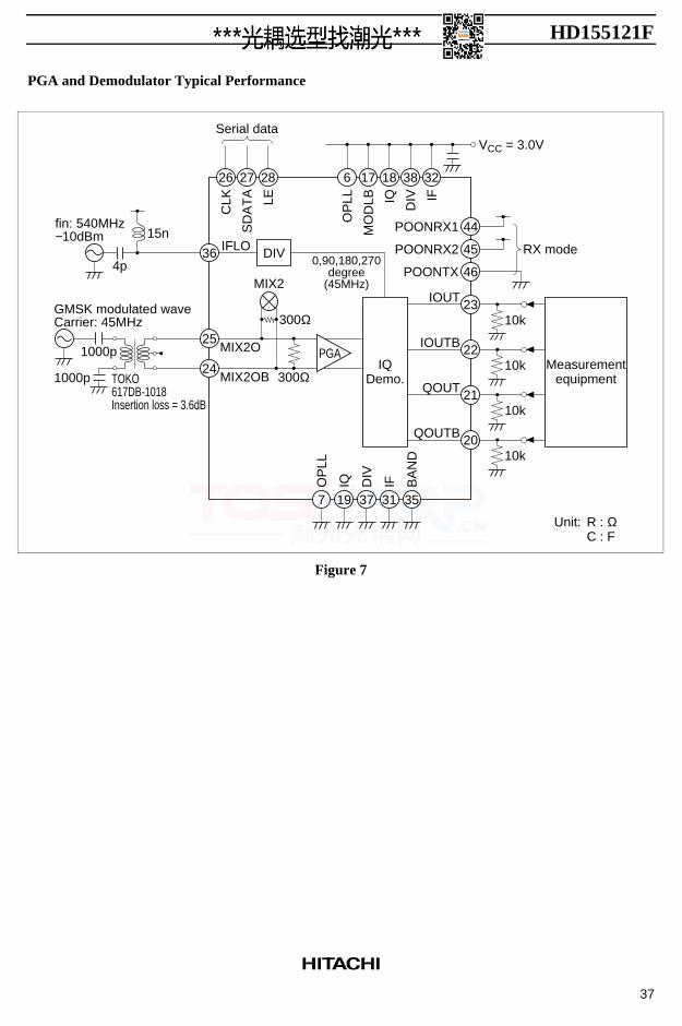
PGA and Demodulator Typical Performance
Unit: R : ΩC : F
OP
LL
VCC = 3.0V
RX mode
MO
DLB
6
IQ
17
DIV
18
IF
38 32
CLK
SD
AT
A
26
LE
OP
LL
27
Serial data
28
IFLO
fin: 540MHz−10dBm
MIX2O
15n
4p36
MIX2
300Ω
300Ω
GMSK modulated waveCarrier: 45MHz
TOKO617DB-1018Insertion loss = 3.6dB
DIV
MIX2OB
25
24PGA1000p
1000p
7
IQ
19
DIV
37
IF
31
BA
ND
35
44POONRX1
45POONRX2
46
10k
POONTX
23IOUT
10k22IOUTB
10k
10k
21QOUT
20QOUTB
IQDemo.
Measurementequipment
0,90,180,270degree
(45MHz)
Figure 7
HD155121F
38
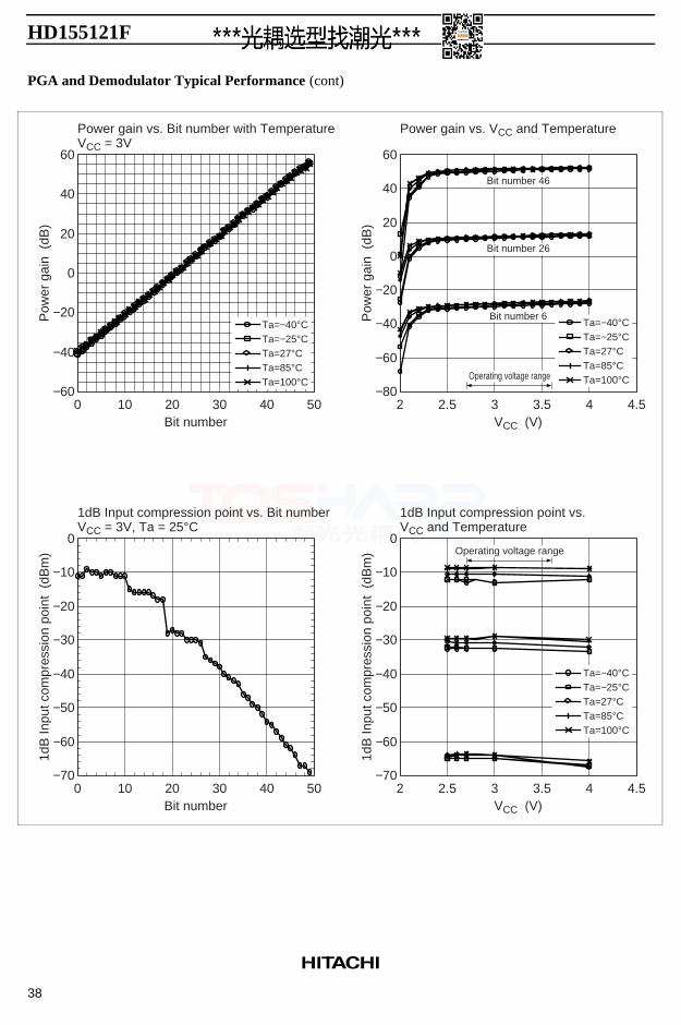
PGA and Demodulator Typical Performance (cont)
504030Bit number20100
504030Bit number20100
Power gain vs. Bit number with TemperatureVCC = 3V
−60
40
20
0
−20
−40
60
Pow
er g
ain
(dB
)1d
B In
put c
ompr
essi
on p
oint
(dB
m)
1dB Input compression point vs. Bit numberVCC = 3V, Ta = 25°C
4.543.5VCC (V)32.52
Power gain vs. VCC and Temperature
4.543.5VCC (V)32.52
1dB Input compression point vs.VCC and Temperature
1dB
Inpu
t com
pres
sion
poi
nt (
dBm
) Operating voltage range
−70
−60
−50
−40
−30
−20
−10
0
−70
−60
−50
−40
−30
−20
−10
0
−80
40
20
0
−20
−40
−60
60
Pow
er g
ain
(dB
)
Ta=−25°CTa=27°CTa=85°CTa=100°C
Ta=−40°CTa=−25°CTa=27°CTa=85°CTa=100°C
Ta=−40°C
Operating voltage range
Bit number 6
Bit number 26
Bit number 46
Ta=−25°CTa=27°CTa=85°CTa=100°C
Ta=−40°C
HD155121F
39
PGA and Demodulator Typical Performance (cont)
100000Frequency (kHz)
1000 1000010010
Frequency (kHz)
10
120
200
400
600
800
1600
3000
20000
sim.(typ)
0.0
−1.2
−4.0
−14.0
−22.3
−29.2
−49.8
−47.3
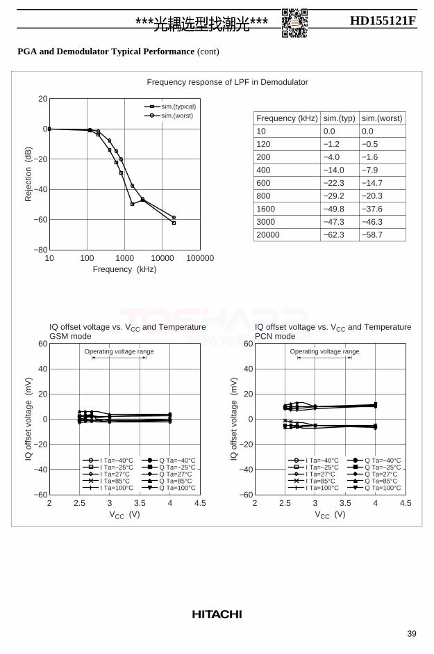
−62.3
sim.(worst)
0.0
−0.5
−1.6
−7.9
−14.7
−20.3
−37.6
−46.3
−58.7
Frequency response of LPF in Demodulator
−80
0
−20
−40
−60
20
Rej
ectio
n (
dB)
IQ o
ffset
vol
tage
(m
V)
IQ offset voltage vs. VCC and TemperatureGSM mode
4.543.5VCC (V)32.524.543.5
VCC (V)32.52
IQ offset voltage vs. VCC and TemperaturePCN mode
IQ o
ffset
vol
tage
(m
V)
Operating voltage range
−60
−40
−20
0
20
40
60
−60
−40
−20
0
20
40
60
sim.(typical)sim.(worst)
Operating voltage range
I Ta=−25°C
I Ta=85°CI Ta=100°C
I Ta=27°C
I Ta=−40°CQ Ta=−25°C
Q Ta=85°CQ Ta=100°C
Q Ta=27°C
Q Ta=−40°CI Ta=−25°C
I Ta=85°CI Ta=100°C
I Ta=27°C
I Ta=−40°CQ Ta=−25°C
Q Ta=85°CQ Ta=100°C
Q Ta=27°C
Q Ta=−40°C
HD155121F
40
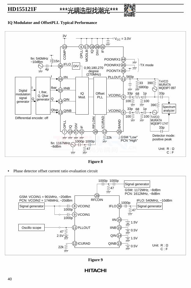
IQ Modulator and OffsetPLL Typical Performance
Unit: R : ΩC : F
OP
LL
VCC = 3.0V
TX mode
MO
DLB
6
IQ
17
DIV
18
IF
38 32
CO
MP
10
OP
LL
3V
IFLO
fin: 540MHz−10dBm
GSM "Low"PCN "High"
TxVCOMURATAMQE9P7-1747
TxVCOMURATAMQE9P7-897
fin: 1167MHz−8dBm
0,90,180,270degree
(270MHz)
15n
4p
IINI
36 DIV
7
IQ
19
DIV
37
IF
31
RF
LOIN
39
ICU
RA
D
12
BA
ND
35
44POONRX1
45POONRX2
46
336800p
POONTX
11PLLOUT
9VCOIN1IQMod.
I, Ibar,Q, Qbar
generator
OffsetPLL
16
IINBIbarDigital
modulationsignal
generator
15
QINBQbar13
QIN
Differential encode: off
Detector mode:positive peak
Q
I
Q14
560p
33p 68
100 100390
1p 33p
33p
8VCOIN233p 68
100 100
22k
47
1pSpectrumanalyzer
390
1000p1000p
Figure 8
• Phase detector offset current ratio evaluation circuit
Unit: R : ΩC : F
VCOIN28
Signal generator
GSM: 1172MHz, −8dBmPCN: 1612MHz, −8dBm
GSM: VCOIN1 = 901MHz, −20dBmPCN: VCOIN2 = 1746MHz, −20dBm IFLO: 540MHz, −10dBm
36IFLO
47
22k
2.5V
RFLOIN
47
1000p1000p
Signal generator
13QINB
Signal generator
39
47
1000p
1000p
VCOIN191000p
PLLOUT11
ICURAD12
Oscillo scope
0.5V
14QIN1.5V
15IINB0.5V
16IIN1.5V
Figure 9

HD155121F
41
IQ Modulator and OffsetPLL Typical Performance (cont)
12040200 60 80 100Temperature (°C)
4.543.5VCC (V)32.52
Tx spectrum vs. TemperatureGSM mode (902MHz)
Tx spectrum vs. VCCGSM mode (902MHz)
Tx spectrum vs. VCCPCN mode (1747MHz)
0
20
40
60
80
100
Sup
pres
sion
rat
io (
dBc)
4.543.5VCC (V)32.52
0
20
40
60
80
100
Sup
pres
sion
rat
io (
dBc)
−60 −20−40
0
20
40
60
80
100
Sup
pres
sion
rat
io (
dBc)
Carrier suppression ratio
Side-band suppression ratio
Operating voltage range
Operating voltage range Operating voltage range
12040200 60 80 100Temperature (°C)
Tx spectrum vs. TemperaturePCN mode (1747MHz)
0
20
40
60
80
100
Sup
pres
sion
rat
io (
dBc)
−60 −20−40
Carrier suppression ratio
Side-band suppression ratio
Operating voltage range
Carrier suppression ratio
Side-band suppression ratio
Carrier suppression ratio
Side-band suppression ratio
HD155121F
42
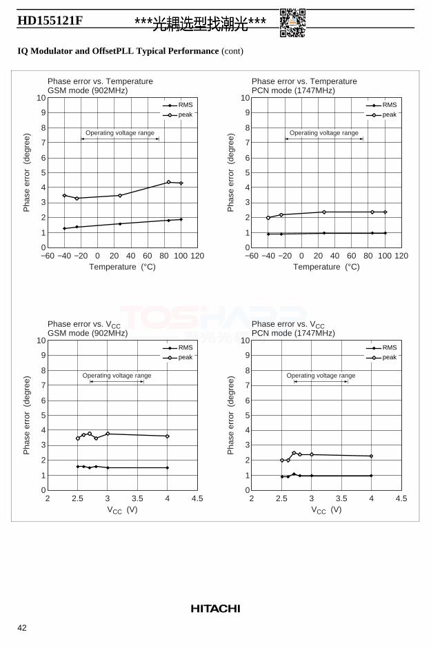
IQ Modulator and OffsetPLL Typical Performance (cont)
12040200 60 80 100Temperature (°C)
4.543.5VCC (V)32.52
Phase error vs. TemperatureGSM mode (902MHz)
Phase error vs. VCCGSM mode (902MHz)
Phase error vs. VCCPCN mode (1747MHz)
0
2
4
6
8
7
5
3
1
9
10
Pha
se e
rror
(de
gree
)
4.543.5VCC (V)32.52
0
2
4
6
8
7
5
3
1
9
10
0
2
4
6
8
7
5
3
1
9
10
Pha
se e
rror
(de
gree
)
−60 −20−40
0
2
4
6
8
7
5
3
1
9
10
Pha
se e
rror
(de
gree
)
RMS
peak
Operating voltage range
Operating voltage range Operating voltage range
12040200 60 80 100Temperature (°C)
Phase error vs. TemperaturePCN mode (1747MHz)
Pha
se e
rror
(de
gree
)
−60 −20−40
Operating voltage range
RMS
peak
RMS
peak
RMS
peak
HD155121F
43
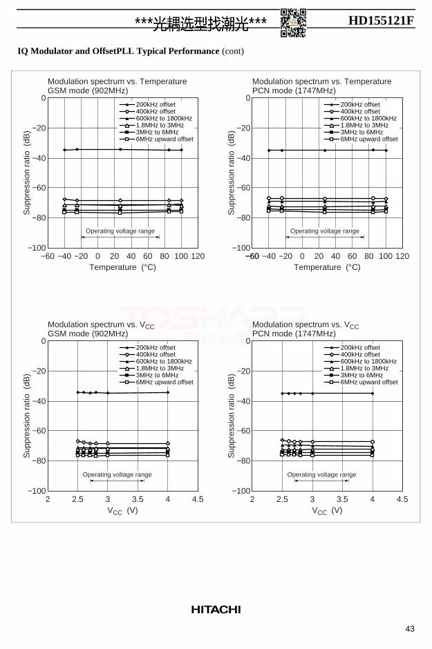
IQ Modulator and OffsetPLL Typical Performance (cont)
12040200 60 80 100Temperature (°C)
4.543.5VCC (V)32.5
Modulation spectrum vs. TemperatureGSM mode (902MHz)
Modulation spectrum vs. VCCGSM mode (902MHz)
Modulation spectrum vs. VCCPCN mode (1747MHz)
−100
−80
−60
−40
−20
0
−100
−80
−60
−40
−20
0
−100
−80
−60
−40
−20
0
Sup
pres
sion
rat
io (
dB)
4.543.5VCC (V)32.522
Sup
pres
sion
rat
io (
dB)
−60−100
−80
−60
−40
−20
0
−60−20−40
Sup
pres
sion
rat
io (
dB)
12040200 60 80 100Temperature (°C)
Modulation spectrum vs. TemperaturePCN mode (1747MHz)
Sup
pres
sion
rat
io (
dB)
−60 −20−40
200kHz offset400kHz offset600kHz to 1800kHz
3MHz to 6MHz6MHz upward offset
1.8MHz to 3MHz
Operating voltage range
200kHz offset400kHz offset600kHz to 1800kHz
3MHz to 6MHz6MHz upward offset
1.8MHz to 3MHz
Operating voltage range
200kHz offset400kHz offset600kHz to 1800kHz
3MHz to 6MHz6MHz upward offset
1.8MHz to 3MHz
200kHz offset400kHz offset600kHz to 1800kHz
3MHz to 6MHz6MHz upward offset
1.8MHz to 3MHz
Operating voltage range Operating voltage range
HD155121F
44
IQ Modulator and OffsetPLL Typical Performance (cont)
12040200 60 80 100Temperature (°C)
4.543.5VCC (V)32.5
Lock up time vs. TemperatureGSM mode (902MHz)
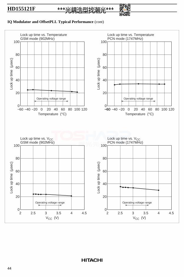
Lock up time vs. VCCGSM mode (902MHz)
Lock up time vs. VCCPCN mode (1747MHz)
0
20
40
60
80
100
0
20
40
60
80
100
0
20
40
60
80
100
Lock
up
time
(µs
ec)
4.543.5VCC (V)32.522
Lock
up
time
(µs
ec)
−600
20
40
60
80
100
−60−20−40
Lock
up
time
(µs
ec)
12040200 60 80 100Temperature (°C)
Lock up time vs. TemperaturePCN mode (1747MHz)
Lock
up
time
(µs
ec)
−60 −20−40
Operating voltage range
Operating voltage range Operating voltage range
Operating voltage range
HD155121F
45
IQ Modulator and OffsetPLL Typical Performance (cont)
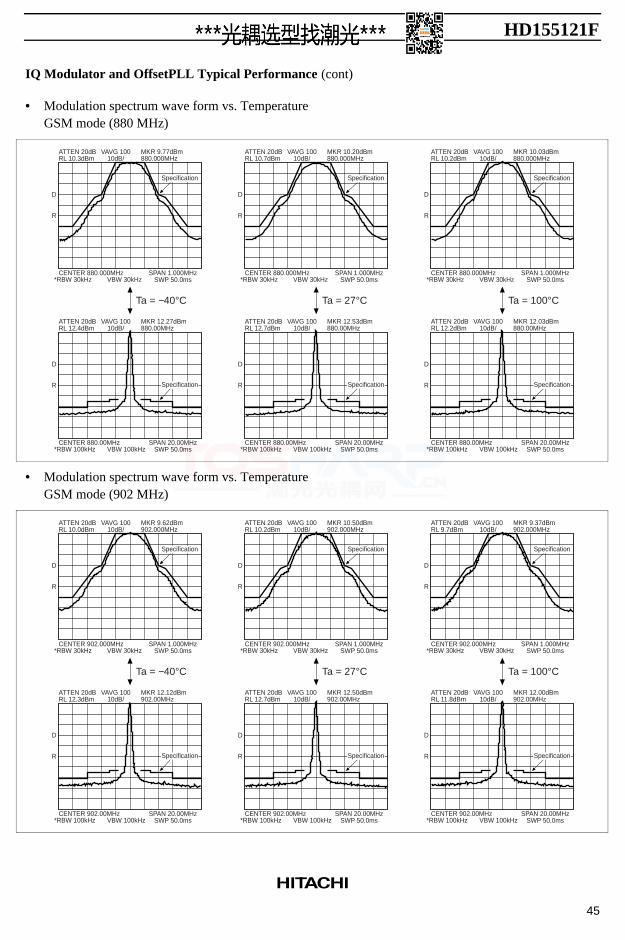
• Modulation spectrum wave form vs. TemperatureGSM mode (880 MHz)
D
ATTEN 20dBRL 10.3dBm
CENTER 880.000MHz SPAN 1.000MHzSWP 50.0ms*RBW 30kHz VBW 30kHz
Ta = −40°C
MKR 9.77dBm880.000MHz
VAVG 10010dB/
R
D
ATTEN 20dBRL 10.7dBm
CENTER 880.000MHz SPAN 1.000MHzSWP 50.0ms*RBW 30kHz VBW 30kHz
MKR 10.20dBm880.000MHz
VAVG 10010dB/
R
D
ATTEN 20dBRL 10.2dBm
CENTER 880.000MHz SPAN 1.000MHzSWP 50.0ms*RBW 30kHz VBW 30kHz
MKR 10.03dBm880.000MHz
VAVG 10010dB/
R
D
ATTEN 20dBRL 12.4dBm
CENTER 880.00MHz SPAN 20.00MHzSWP 50.0ms*RBW 100kHz VBW 100kHz
MKR 12.27dBm880.00MHz
VAVG 10010dB/
R
D
ATTEN 20dBRL 12.7dBm
CENTER 880.00MHz SPAN 20.00MHzSWP 50.0ms*RBW 100kHz VBW 100kHz
MKR 12.53dBm880.00MHz
VAVG 10010dB/
R
D
ATTEN 20dBRL 12.2dBm
CENTER 880.00MHz SPAN 20.00MHzSWP 50.0ms*RBW 100kHz VBW 100kHz
MKR 12.03dBm880.00MHz
VAVG 10010dB/
R
Ta = 27°C Ta = 100°C
Specification
Specification Specification Specification
Specification Specification
• Modulation spectrum wave form vs. TemperatureGSM mode (902 MHz)
D
ATTEN 20dBRL 10.0dBm
CENTER 902.000MHz SPAN 1.000MHzSWP 50.0ms*RBW 30kHz VBW 30kHz
Ta = −40°C
MKR 9.62dBm902.000MHz
VAVG 10010dB/
R
D
ATTEN 20dBRL 10.2dBm
CENTER 902.000MHz SPAN 1.000MHzSWP 50.0ms*RBW 30kHz VBW 30kHz
MKR 10.50dBm902.000MHz
VAVG 10010dB/
R
D
ATTEN 20dBRL 9.7dBm
CENTER 902.000MHz SPAN 1.000MHzSWP 50.0ms*RBW 30kHz VBW 30kHz
MKR 9.37dBm902.000MHz
VAVG 10010dB/
R
D
ATTEN 20dBRL 12.3dBm
CENTER 902.00MHz SPAN 20.00MHzSWP 50.0ms*RBW 100kHz VBW 100kHz
MKR 12.12dBm902.00MHz
VAVG 10010dB/
R
D
ATTEN 20dBRL 12.7dBm
CENTER 902.00MHz SPAN 20.00MHzSWP 50.0ms*RBW 100kHz VBW 100kHz
MKR 12.50dBm902.00MHz
VAVG 10010dB/
R
D
ATTEN 20dBRL 11.8dBm
CENTER 902.00MHz SPAN 20.00MHzSWP 50.0ms*RBW 100kHz VBW 100kHz
MKR 12.00dBm902.00MHz
VAVG 10010dB/
R
Ta = 27°C Ta = 100°C
Specification
Specification Specification Specification
Specification Specification
HD155121F
46
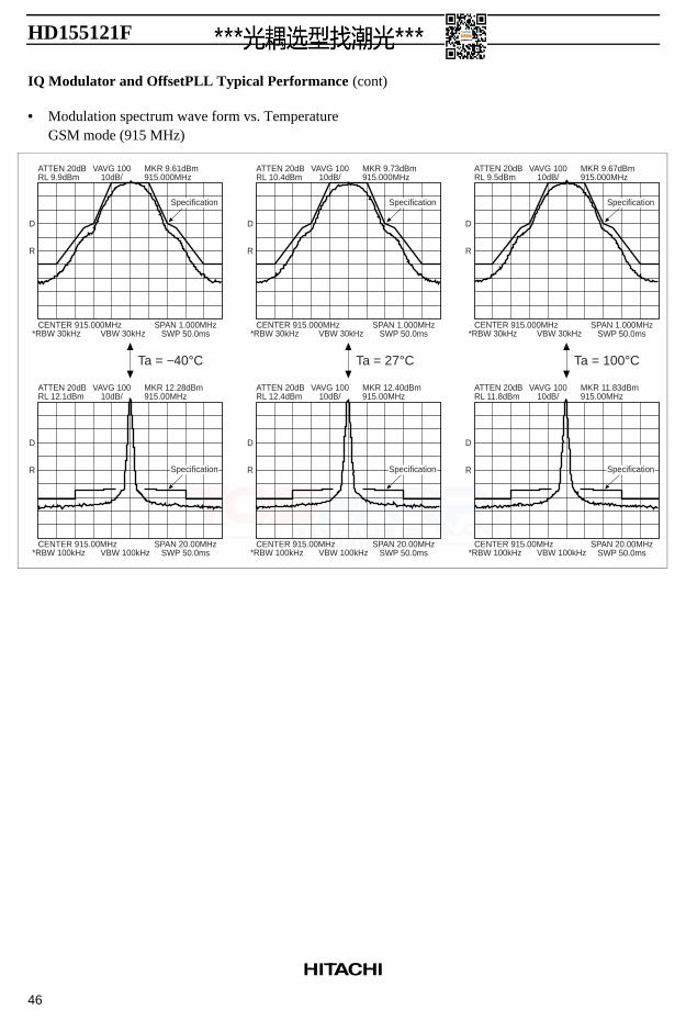
IQ Modulator and OffsetPLL Typical Performance (cont)
• Modulation spectrum wave form vs. TemperatureGSM mode (915 MHz)
D
ATTEN 20dBRL 9.9dBm
CENTER 915.000MHz SPAN 1.000MHzSWP 50.0ms*RBW 30kHz VBW 30kHz
Ta = −40°C
MKR 9.61dBm915.000MHz
VAVG 10010dB/
R
D
ATTEN 20dBRL 10.4dBm
CENTER 915.000MHz SPAN 1.000MHzSWP 50.0ms*RBW 30kHz VBW 30kHz
MKR 9.73dBm915.000MHz
VAVG 10010dB/
R
D
ATTEN 20dBRL 9.5dBm
CENTER 915.000MHz SPAN 1.000MHzSWP 50.0ms*RBW 30kHz VBW 30kHz
MKR 9.67dBm915.000MHz
VAVG 10010dB/
R
D
ATTEN 20dBRL 12.1dBm
CENTER 915.00MHz SPAN 20.00MHzSWP 50.0ms*RBW 100kHz VBW 100kHz
MKR 12.28dBm915.00MHz
VAVG 10010dB/
R
D
ATTEN 20dBRL 12.4dBm
CENTER 915.00MHz SPAN 20.00MHzSWP 50.0ms*RBW 100kHz VBW 100kHz
MKR 12.40dBm915.00MHz
VAVG 10010dB/
R
D
ATTEN 20dBRL 11.8dBm
CENTER 915.00MHz SPAN 20.00MHzSWP 50.0ms*RBW 100kHz VBW 100kHz
MKR 11.83dBm915.00MHz
VAVG 10010dB/
R
Ta = 27°C Ta = 100°C
Specification
Specification Specification Specification
Specification Specification
HD155121F
47
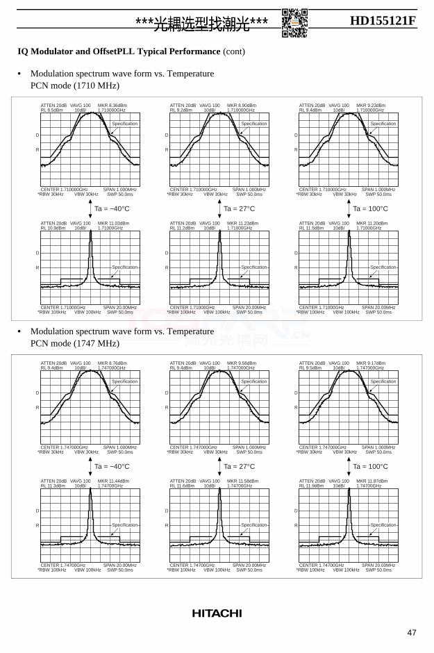
IQ Modulator and OffsetPLL Typical Performance (cont)
• Modulation spectrum wave form vs. TemperaturePCN mode (1710 MHz)
D
ATTEN 20dBRL 8.5dBm
CENTER 1.710000GHz SPAN 1.000MHzSWP 50.0ms*RBW 30kHz VBW 30kHz
Ta = −40°C
MKR 8.36dBm1.710000GHz
VAVG 10010dB/
R
D
ATTEN 20dBRL 9.2dBm
CENTER 1.710000GHz SPAN 1.000MHzSWP 50.0ms*RBW 30kHz VBW 30kHz
MKR 8.90dBm1.710000GHz
VAVG 10010dB/
R
D
ATTEN 20dBRL 9.4dBm
CENTER 1.710000GHz SPAN 1.000MHzSWP 50.0ms*RBW 30kHz VBW 30kHz
MKR 9.23dBm1.710000GHz
VAVG 10010dB/
R
D
ATTEN 20dBRL 10.9dBm
CENTER 1.71000GHz SPAN 20.00MHzSWP 50.0ms*RBW 100kHz VBW 100kHz
MKR 11.03dBm1.71000GHz
VAVG 10010dB/
R
D
ATTEN 20dBRL 11.2dBm
CENTER 1.71000GHz SPAN 20.00MHzSWP 50.0ms*RBW 100kHz VBW 100kHz
MKR 11.23dBm1.71000GHz
VAVG 10010dB/
R
D
ATTEN 20dBRL 11.5dBm
CENTER 1.71000GHz SPAN 20.00MHzSWP 50.0ms*RBW 100kHz VBW 100kHz
MKR 11.20dBm1.71000GHz
VAVG 10010dB/
R
Ta = 27°C Ta = 100°C
Specification
Specification Specification Specification
Specification Specification
• Modulation spectrum wave form vs. TemperaturePCN mode (1747 MHz)
D
ATTEN 20dBRL 9.4dBm
CENTER 1.747000GHz SPAN 1.000MHzSWP 50.0ms*RBW 30kHz VBW 30kHz
Ta = −40°C
MKR 8.76dBm1.747000GHz
VAVG 10010dB/
R
D
ATTEN 20dBRL 9.4dBm
CENTER 1.747000GHz SPAN 1.000MHzSWP 50.0ms*RBW 30kHz VBW 30kHz
MKR 9.58dBm1.747000GHz
VAVG 10010dB/
R
D
ATTEN 20dBRL 9.5dBm
CENTER 1.747000GHz SPAN 1.000MHzSWP 50.0ms*RBW 30kHz VBW 30kHz
MKR 9.17dBm1.747000GHz
VAVG 10010dB/
R
D
ATTEN 20dBRL 11.3dBm
CENTER 1.74700GHz SPAN 20.00MHzSWP 50.0ms*RBW 100kHz VBW 100kHz
MKR 11.44dBm1.74700GHz
VAVG 10010dB/
R
D
ATTEN 20dBRL 11.6dBm
CENTER 1.74700GHz SPAN 20.00MHzSWP 50.0ms*RBW 100kHz VBW 100kHz
MKR 11.58dBm1.74700GHz
VAVG 10010dB/
R
D
ATTEN 20dBRL 11.9dBm
CENTER 1.74700GHz SPAN 20.00MHzSWP 50.0ms*RBW 100kHz VBW 100kHz
MKR 11.87dBm1.74700GHz
VAVG 10010dB/
R
Ta = 27°C Ta = 100°C
Specification
Specification Specification Specification
Specification Specification

HD155121F
48
IQ Modulator and OffsetPLL Typical Performance (cont)
• Modulation spectrum wave form vs. TemperaturePCN mode (1785 MHz)
D
ATTEN 20dBRL 8.8dBm
CENTER 1.785000GHz SPAN 1.000MHzSWP 50.0ms*RBW 30kHz VBW 30kHz
Ta = −40°C
MKR 8.44dBm1.785000GHz
VAVG 10010dB/
R
D
ATTEN 20dBRL 8.7dBm
CENTER 1.785000GHz SPAN 1.000MHzSWP 50.0ms*RBW 30kHz VBW 30kHz
MKR 8.91dBm1.785000GHz
VAVG 10010dB/
R
D
ATTEN 20dBRL 9.4dBm
CENTER 1.785000GHz SPAN 1.000MHzSWP 50.0ms*RBW 30kHz VBW 30kHz
MKR 9.57dBm1.785000GHz
VAVG 10010dB/
R
D
ATTEN 20dBRL 11.3dBm
CENTER 1.78500GHz SPAN 20.00MHzSWP 50.0ms*RBW 100kHz VBW 100kHz
MKR 10.94dBm1.78500GHz
VAVG 10010dB/
R
D
ATTEN 20dBRL 11.4dBm
CENTER 1.78500GHz SPAN 20.00MHzSWP 50.0ms*RBW 100kHz VBW 100kHz
MKR 11.41dBm1.78500GHz
VAVG 10010dB/
R
D
ATTEN 20dBRL 11.8dBm
CENTER 1.78500GHz SPAN 20.00MHzSWP 50.0ms*RBW 100kHz VBW 100kHz
MKR 11.66dBm1.78500GHz
VAVG 10010dB/
R
Ta = 27°C Ta = 100°C
Specification
Specification Specification Specification
Specification Specification
HD155121F
49
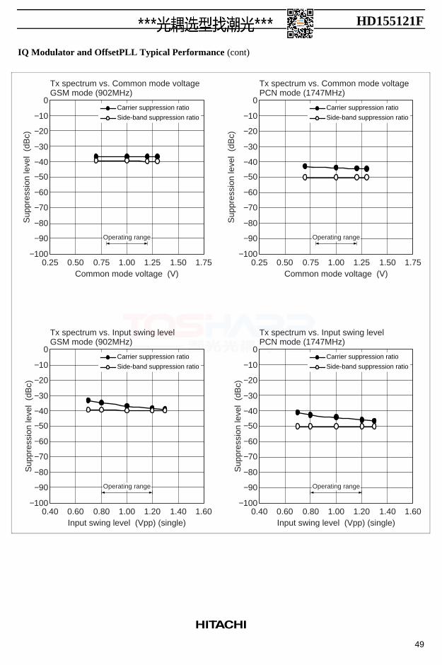
IQ Modulator and OffsetPLL Typical Performance (cont)
Common mode voltage (V)
Input swing level (Vpp) (single)
Tx spectrum vs. Input swing levelGSM mode (902MHz)
Tx spectrum vs. Input swing levelPCN mode (1747MHz)
Sup
pres
sion
leve
l (d
Bc)
Input swing level (Vpp) (single)
Sup
pres
sion
leve
l (d
Bc)
Sup
pres
sion
leve
l (d
Bc)
1.601.000.80 1.20 1.40−100
−80
−60
−40
−20
0
−10
−30
−70
−90
−50
0.40 0.60 1.601.000.80 1.20 1.40−100
−80
−60
−40
−20
0
−10
−30
−70
−90
−50
0.40 0.60
−100
−80
−60
−40
−20
0
−10
−30
−70
−90
−50
−100
−80
−60
−40
−20
0
−10
−30
−70
−90
−50
1.751.000.75 1.25 1.500.25 0.50Common mode voltage (V)
1.751.000.75 1.25 1.500.25 0.50
Tx spectrum vs. Common mode voltageGSM mode (902MHz)
Sup
pres
sion
leve
l (d
Bc)
Tx spectrum vs. Common mode voltagePCN mode (1747MHz)
Operating range
Operating range Operating range
Operating range
Carrier suppression ratio
Side-band suppression ratio
Carrier suppression ratio
Side-band suppression ratio
Carrier suppression ratio
Side-band suppression ratio
Carrier suppression ratio
Side-band suppression ratio
HD155121F
50
IQ Modulator and OffsetPLL Typical Performance (cont)
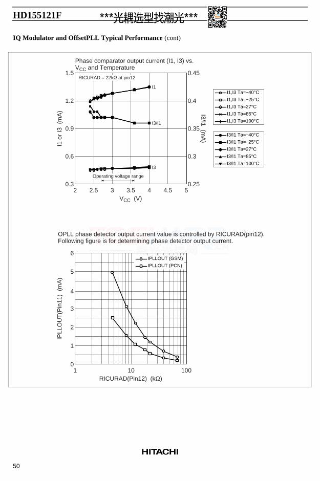
RICURAD(Pin12) (kΩ)
Phase comparator output current (I1, I3) vs.VCC and Temperature
0.3
0.6
0.9
1.5
1.2
0.25
0.3
0.35
0.45
0.4
I3/I1 (mA
)
I1 o
r I3
(m
A)
OPLL phase detector output current value is controlled by RICURAD(pin12).Following figure is for determining phase detector output current.
IPLL
OU
T(P
in11
) (
mA
)
100100
1
2
3
4
5
6
1
54.543.5VCC (V)
32.52
Operating voltage range
I1
I3/I1
I3
I1,I3 Ta=−40°CI1,I3 Ta=−25°CI1,I3 Ta=27°CI1,I3 Ta=85°CI1,I3 Ta=100°C
I3/I1 Ta=−40°CI3/I1 Ta=−25°CI3/I1 Ta=27°CI3/I1 Ta=85°CI3/I1 Ta=100°C
RICURAD = 22kΩ at pin12
IPLLOUT (GSM)
IPLLOUT (PCN)
HD155121F
51
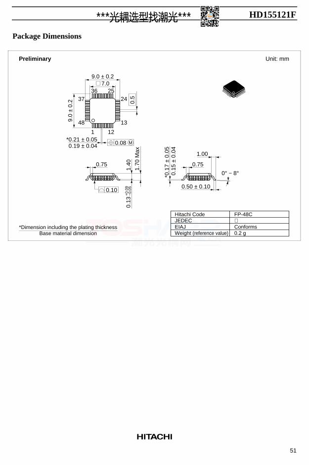
Package Dimensions
Preliminary
Hitachi CodeJEDECEIAJWeight (reference value)
FP-48CConforms0.2 g
Unit: mm
*Dimension including the plating thicknessBase material dimension
9.0 ± 0.27.0
*0.21 ± 0.050.08
36 25
1 12
37
48
24
13
0.5
9.0
± 0.
2
0.10
1.00
0° − 8°
0.50 ± 0.10
*0.1
7 ±
0.05
1.70
Max
M
0.75 0.75
0.19 ± 0.04
1.40
0.15
± 0
.04
0.13
+0.
09−0
.05
HD155121F
52
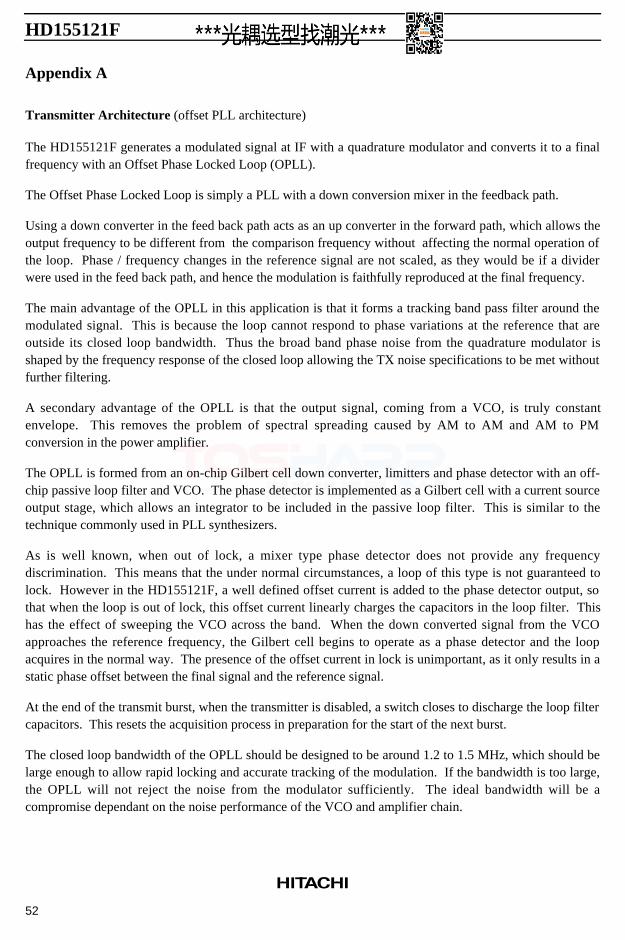
Appendix A
Transmitter Architecture (offset PLL architecture)
The HD155121F generates a modulated signal at IF with a quadrature modulator and converts it to a finalfrequency with an Offset Phase Locked Loop (OPLL).
The Offset Phase Locked Loop is simply a PLL with a down conversion mixer in the feedback path.
Using a down converter in the feed back path acts as an up converter in the forward path, which allows theoutput frequency to be different from the comparison frequency without affecting the normal operation ofthe loop. Phase / frequency changes in the reference signal are not scaled, as they would be if a dividerwere used in the feed back path, and hence the modulation is faithfully reproduced at the final frequency.
The main advantage of the OPLL in this application is that it forms a tracking band pass filter around themodulated signal. This is because the loop cannot respond to phase variations at the reference that areoutside its closed loop bandwidth. Thus the broad band phase noise from the quadrature modulator isshaped by the frequency response of the closed loop allowing the TX noise specifications to be met withoutfurther filtering.
A secondary advantage of the OPLL is that the output signal, coming from a VCO, is truly constantenvelope. This removes the problem of spectral spreading caused by AM to AM and AM to PMconversion in the power amplifier.
The OPLL is formed from an on-chip Gilbert cell down converter, limitters and phase detector with an off-chip passive loop filter and VCO. The phase detector is implemented as a Gilbert cell with a current sourceoutput stage, which allows an integrator to be included in the passive loop filter. This is similar to thetechnique commonly used in PLL synthesizers.
As is well known, when out of lock, a mixer type phase detector does not provide any frequencydiscrimination. This means that the under normal circumstances, a loop of this type is not guaranteed tolock. However in the HD155121F, a well defined offset current is added to the phase detector output, sothat when the loop is out of lock, this offset current linearly charges the capacitors in the loop filter. Thishas the effect of sweeping the VCO across the band. When the down converted signal from the VCOapproaches the reference frequency, the Gilbert cell begins to operate as a phase detector and the loopacquires in the normal way. The presence of the offset current in lock is unimportant, as it only results in astatic phase offset between the final signal and the reference signal.
At the end of the transmit burst, when the transmitter is disabled, a switch closes to discharge the loop filtercapacitors. This resets the acquisition process in preparation for the start of the next burst.
The closed loop bandwidth of the OPLL should be designed to be around 1.2 to 1.5 MHz, which should belarge enough to allow rapid locking and accurate tracking of the modulation. If the bandwidth is too large,the OPLL will not reject the noise from the modulator sufficiently. The ideal bandwidth will be acompromise dependant on the noise performance of the VCO and amplifier chain.
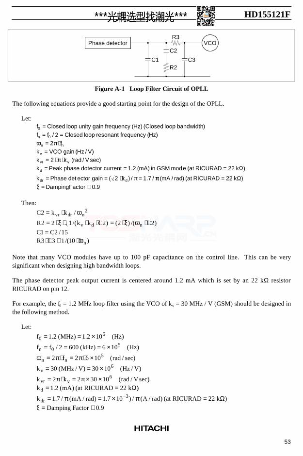
HD155121F
53
C3
R3Phase detector VCO
C2
R2C1
Figure A-1 Loop Filter Circuit of OPLL
The following equations provide a good starting point for the design of the OPLL.
Let:f Closed loop unity gain frequency Hz Closed loop bandwidth
f f Closed loop resonant frequency Hz
fk VCO gain Hz Vk k rad Vk Peak phase dotector current mA in GSM e at RICURAD k
k Phase ector gain k
n
n n
v
vr v
d
dr d
0
0 2
2
21 2 22
2 1 7
== =
= ⋅== ⋅ ⋅= = =
= = ⋅ =
( ) ( )
/ ( )
( / )( / sec)
. ( ) mod ( )
det ( ) / . /
ω π
π
π
Ω
ππξ
( / ) ( )
.
mA rad at RICURAD k
DampingFactor
== ≅
22
0 9
Ω
Then:
C k k
R k k C C
C CR C
vr dr n
v d n
n
2
2 2 1 2 2 2
1 2 153 3 1 10
2= ⋅= ⋅ ⋅ ⋅ ⋅ = ⋅ ⋅=⋅ ≅ ⋅
/
/( ) ( ) /( )
//( )
ωξ ξ ω
ω
Note that many VCO modules have up to 100 pF capacitance on the control line. This can be verysignificant when designing high bandwidth loops.
The phase detector peak output current is centered around 1.2 mA which is set by an 22 kΩ resistorRICURAD on pin 12.
For example, the f0 = 1.2 MHz loop filter using the VCO of kv = 30 MHz / V (GSM) should be designed inthe following method.
Let:
f MHz Hz
f f kHz Hz
f rad
k MHz V Hz V
k k rad Vk mA at RICURAD k
n
n n
v
vr v
d
06
05
5
6
6
1 2 1 2 10
2 600 6 10
2 2 6 10
30 30 10
2 2 30 101 2 22
= = ×
= = = ×
= ⋅ = ⋅ ×
= = ×
= ⋅ = × ×= =
. ( ) . ( )
/ ( ) ( )
( / sec)
( / ) ( / )
( / sec). ( ) (
ω π π
π πΩ))
. / ( / ) . ) / ( / ) ( )
.
k mA rad A rad at RICURAD k
Damping Factordr = = × == ≅
−1 7 1 7 10 22
0 9
3π πξ
Ω
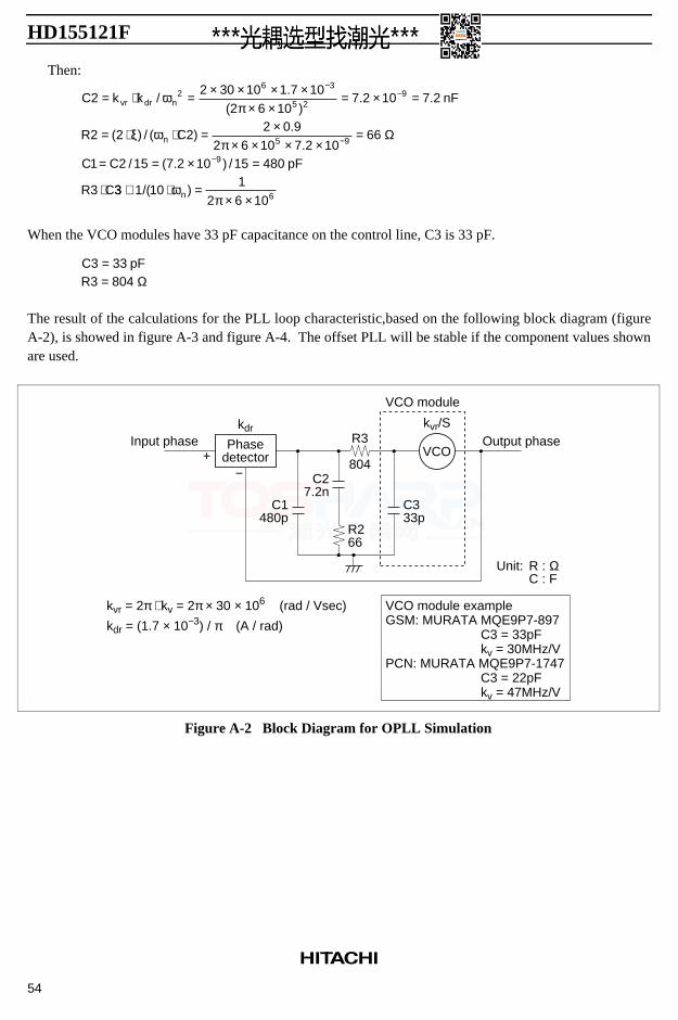
HD155121F
54
Then:
C k k nF
R C
C C pF
R C
vr dr n
n
22 30 10 1 7 10
2 6 107 2 10 7 2
2 2 22 0 9
2 6 10 7 2 1066
1 2 15 7 2 10 15 480
3
26 3
5 29
5 9
9
= ⋅ = × × × ×× ×
= × =
= ⋅ ⋅ = ×× × × ×
=
= = × =
⋅
−−
−
−
/.
( ). .
( ) / ( ).
./ ( . ) /
ωπ
ξ ωπ
Ω
33 1 101
2 6 106≅ ⋅ =× ×
/( )ωπn
When the VCO modules have 33 pF capacitance on the control line, C3 is 33 pF.
C pFR
3 333 804
== Ω
The result of the calculations for the PLL loop characteristic,based on the following block diagram (figureA-2), is showed in figure A-3 and figure A-4. The offset PLL will be stable if the component values shownare used.
C333p
R3
804
VCO module
Input phase Output phasekdr
+−
kvr/S
kvr = 2π ⋅ kv = 2π × 30 × 106 (rad / Vsec)
kdr = (1.7 × 10⁻³) / π (A / rad)
VCO module exampleGSM: MURATA MQE9P7-897
PCN: MURATA MQE9P7-1747
C3 = 33pFkv = 30MHz/V
C3 = 22pFkv = 47MHz/V
VCO
C27.2n
R266
C1480p
Unit: R : ΩC : F
Phasedetector
Figure A-2 Block Diagram for OPLL Simulation
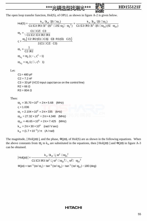
HD155121F
55
The open loop transfer function, Hol(S), of OPLL as shown in figure A-2 is given below.
Hol Sk k S
C C R S S S
k k S
C C R S S S
C C CC C C R RC R
vr dr z
p p
vr dr z
p p
p
p
( )( )
( )
( )
( ) ( )
(
=⋅ ⋅ +
⋅ ⋅ ⋅ ⋅ + ⋅ +=
⋅ ⋅ +⋅ ⋅ ⋅ ⋅ + +
= + +⋅ ⋅ ⋅ ⋅
=⋅
ωω ω
ωω ω
ω
ςω
1 3 3 2 1 3 3
1 2 31 2 3 2 32 2
2 2 2 21 2
CC C C R C C
C C C
C Rz
p p
p p
1 3 3 3 1 2
2 1 2 31
2 2
1
1
12
22
+ + ⋅ + + +
=⋅
= − −
= + −
) ( )
( )
( )
( )
ω
ω ω ς ς
ω ω ς ς
Let:C pFC nFC pF VCO input capci ce on the control lineRR
1 4802 7 23 332 663 804
=====
.( tan )
ΩΩ
Then:ω πςω π
ω π
ω π
π
π
p
z
p
p
vr
dr
MHz
kHz
MHz
MHz
k rad V
k A rad
= × = ×=
= × = ×
= × = ×
= × = ×
= × ×
= × −
35 70 10 2 5 68
1 036
2 104 10 2 335
27 32 10 2 4 348
46 65 10 2 7 425
2 30 10
1 7 10
6
6
16
26
6
3
. . ( )
.
. ( )
. . ( )
. . ( )
( / sec)
( . ) / ( / )
The magnitude, | Hol(jω) |, and the phase, Φ(jω), of Hol(S) are as shown in the following equations. Whenthe above constants from ωp to kdr are substituted in the equations, then | Hol(jω) | and Φ(jω) in figure A-3can be obtained.
Hol jk k
C C R
j
vr dr p
p p
z p p
( )
( ) tan ( / ) tan ( / ) tan ( / ) (deg)
ωω ω
ω ω ω ω ω
ω ω ω ω ω ω ω
=⋅ ⋅ +
⋅ ⋅ ⋅ ⋅ + ⋅ +
= − − −− − −
212
2 212 2
22
1 11
12
1 3 3
180Φ
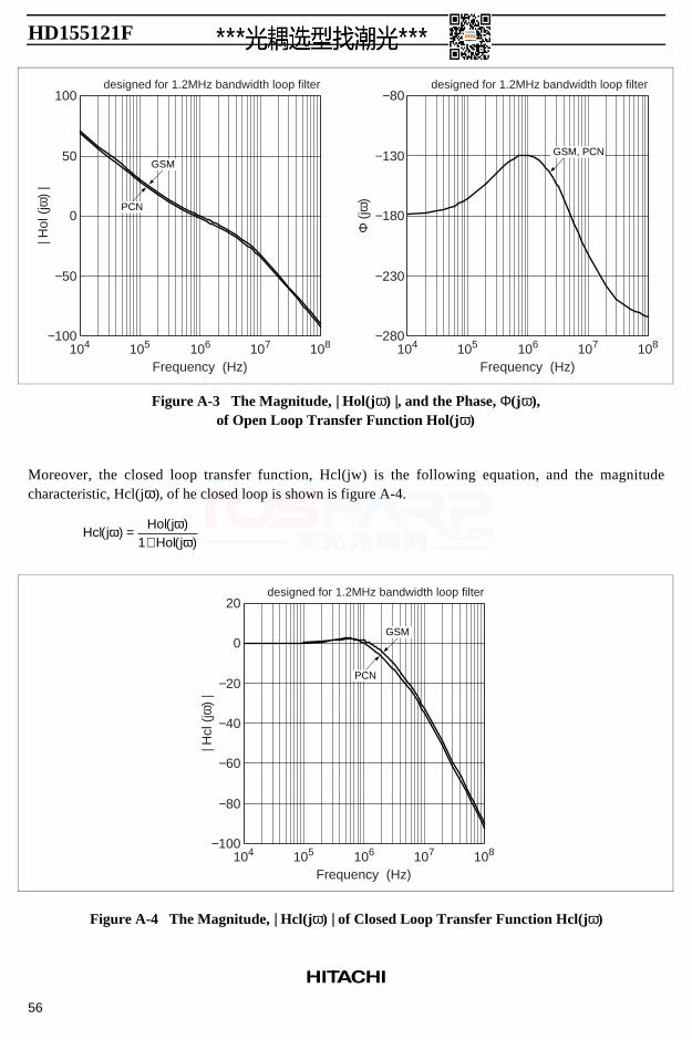
HD155121F
56
108106 107
Frequency (Hz)
designed for 1.2MHz bandwidth loop filter designed for 1.2MHz bandwidth loop filter
−100
−50
0
50
100
| Hol
(jω
) |
104 105 108106 107
Frequency (Hz)
−280
−230
−180
−130
−80
Φ (
jω)
104 105
GSMGSM, PCN
PCN
Figure A-3 The Magnitude, | Hol(jω) |, and the Phase, Φ(jω),of Open Loop Transfer Function Hol(jω)
Moreover, the closed loop transfer function, Hcl(jw) is the following equation, and the magnitudecharacteristic, Hcl(jω), of he closed loop is shown is figure A-4.
Hcl jHol j
Hol j( )
( )( )
ω ωω
=+1
108106 107
Frequency (Hz)
designed for 1.2MHz bandwidth loop filter
−100
−60
−40
−20
−80
0
20
| Hcl
(jω
) |
104 105
GSM
PCN
Figure A-4 The Magnitude, | Hcl(jω) | of Closed Loop Transfer Function Hcl(jω)
HD155121F
57
Cautions
1. Hitachi neither warrants nor grants licenses of any rights of Hitachi’s or any third party’s patent,copyright, trademark, or other intellectual property rights for information contained in this document.Hitachi bears no responsibility for problems that may arise with third party’s rights, includingintellectual property rights, in connection with use of the information contained in this document.
2. Products and product specifications may be subject to change without notice. Confirm that you havereceived the latest product standards or specifications before final design, purchase or use.
3. Hitachi makes every attempt to ensure that its products are of high quality and reliability. However,contact Hitachi’s sales office before using the product in an application that demands especially highquality and reliability or where its failure or malfunction may directly threaten human life or cause riskof bodily injury, such as aerospace, aeronautics, nuclear power, combustion control, transportation,traffic, safety equipment or medical equipment for life support.
4. Design your application so that the product is used within the ranges guaranteed by Hitachi particularlyfor maximum rating, operating supply voltage range, heat radiation characteristics, installationconditions and other characteristics. Hitachi bears no responsibility for failure or damage when usedbeyond the guaranteed ranges. Even within the guaranteed ranges, consider normally foreseeablefailure rates or failure modes in semiconductor devices and employ systemic measures such as fail-safes, so that the equipment incorporating Hitachi product does not cause bodily injury, fire or otherconsequential damage due to operation of the Hitachi product.
5. This product is not designed to be radiation resistant.
6. No one is permitted to reproduce or duplicate, in any form, the whole or part of this document withoutwritten approval from Hitachi.
7. Contact Hitachi’s sales office for any questions regarding this document or Hitachi semiconductorproducts.
Hitachi, Ltd.Semiconductor & Integrated Circuits.Nippon Bldg., 2-6-2, Ohte-machi, Chiyoda-ku, Tokyo 100-0004, JapanTel: Tokyo (03) 3270-2111 Fax: (03) 3270-5109
Copyright © Hitachi, Ltd., 1998. All rights reserved. Printed in Japan.
Hitachi Asia Pte. Ltd.16 Collyer Quay #20-00Hitachi TowerSingapore 049318Tel: 535-2100Fax: 535-1533
URL NorthAmerica : http:semiconductor.hitachi.com/Europe : http://www.hitachi-eu.com/hel/ecgAsia (Singapore) : http://www.has.hitachi.com.sg/grp3/sicd/index.htmAsia (Taiwan) : http://www.hitachi.com.tw/E/Product/SICD_Frame.htmAsia (HongKong) : http://www.hitachi.com.hk/eng/bo/grp3/index.htmJapan : http://www.hitachi.co.jp/Sicd/indx.htm
Hitachi Asia Ltd.Taipei Branch Office3F, Hung Kuo Building. No.167, Tun-Hwa North Road, Taipei (105)Tel: <886> (2) 2718-3666Fax: <886> (2) 2718-8180
Hitachi Asia (Hong Kong) Ltd.Group III (Electronic Components)7/F., North Tower, World Finance Centre,Harbour City, Canton Road, Tsim Sha Tsui,Kowloon, Hong KongTel: <852> (2) 735 9218Fax: <852> (2) 730 0281 Telex: 40815 HITEC HXHitachi Europe Ltd.
Electronic Components Group.Whitebrook ParkLower Cookham RoadMaidenheadBerkshire SL6 8YA, United KingdomTel: <44> (1628) 585000Fax: <44> (1628) 778322
Hitachi Europe GmbHElectronic components GroupDornacher Straße 3D-85622 Feldkirchen, MunichGermanyTel: <49> (89) 9 9180-0Fax: <49> (89) 9 29 30 00
Hitachi Semiconductor (America) Inc.179 East Tasman Drive,San Jose,CA 95134 Tel: <1> (408) 433-1990Fax: <1>(408) 433-0223
For further information write to: