Embed Size (px)
Citation preview

RF MODELLING OF A MULTIPORT AMPLIFIER FOR A MOBILE COMMUNICATIONS SATELLITE
P.James(1), S.V. Potter(1) G. R. Cobb(1) & M. Walden(2)
(1)Astrium Ltd, Portsmouth, Hampshire, PO3 5PU, England. Email: [email protected].
(2)Roke Manor Research Ltd, Romsey, Hampshire, SO51 OZN, England. Email:
Abstract
Some communication satellites have an antenna that consists of a fixed parabolic reflector that is fed by an array. Such antenna systems can be programmed to produce a variety of fixed beams in response to traffic demands and can be built so that each array element is fed by its own high power amplifier. However benefits can accrue if the amplifiers are incorporated into Multiport Power Amplifiers (MPAs). Ideally all the MPA inputs are divided equally between all amplifiers and there is a one to one correspondence between the MPA feed ports and the MPA array ports. Due to imperfections in the INET and the ONET, and differences between the amplifiers, the ideal behaviour is never realized in practice. To optimize the performance of any manufactured MPA a deliberate offset in the gain and phase shift of each amplifier has to be introduced to compensate for the imperfections introduced by the INET, the ONET and their associated cabling. This paper shows how the RF modelling of an MPA has been performed by computer modelling using HFSS, Matlab and the Agilent ADS software.
Introduction Astrium’s experience with Inmarsat has shown that a satellite designed for mobile telecommunications applications may consist of a large aperture parabolic reflector fed by an array at its principle focus. L, S, ku and ka-band are at present the frequencies of interest, [5]. Each radiator element on the array has a one to one correspondence with a spot position on the earth, so that radiation patterns may be pointed at different locations on the earth by different combinations of the array element excitations. Before the signals arrive at the array with their specified complex weights they must undergo amplification, which is provided by a beam forming network composed of between 10 and 20 Multi-Port Amplifiers, [2]. The architecture of an MPA is shown in Figure 1, [7]. The MPA An individual RF signal travels through a multi-port amplifier, going first through a Butler matrix, known as an INET, before being distributed through all the amplifiers and then being concentrated into a single output by a high power Butler matrix and filters, known as an ONET, prior to entering the feed array. An MPA can have (2, 4, 8, 16,…2n ) ports, though at present the interest is in MPAs with 4 and 8 amplifiers, Figure 1.This type of design requires many RF measurements and it would be advantageous if some of these could be avoided by having a computer model. This paper presents the details of the modeling of the MPA. It describes some of the theoretical results of the modelling activity.

Figure 1 An eight way Multi-port amplifier
Modelling Description A MPA may be described mathematically by an INET and ONET connected by amplifiers. The input signal is given as:
Vin1 1 0 0 0 0 0 0 0( ):= (1) The S-parameter matrix for the amplifiers may be expressed as:
S
s1
0
0
0
0
0
0
0
0
s2
0
0
0
0
0
0
0
0
s3
0
0
0
0
0
0
0
0
s4
0
0
0
0
0
0
0
0
s5
0
0
0
0
0
0
0
0
s6
0
0
0
0
0
0
0
0
s7
0
0
0
0
0
0
0
0
s8 (2) Whilst both the INET and ONET may be expressed as
A
1
e
π− i⋅
2
e
π− i⋅
2
eπ i⋅
e
π− i⋅
2
eπ i⋅
eπ i⋅
e
π i⋅
2
e
π− i⋅
2
eπ i⋅
eπ i⋅
e
π i⋅
2
1
e
π− i⋅
2
e
π− i⋅
2
eπ i⋅
e
π− i⋅
2
eπ i⋅
1
e
π− i⋅
2
eπ i⋅
e
π i⋅
2
e
π− i⋅
2
eπ i⋅
eπ i⋅
e
π i⋅
2
e
π− i⋅
2
eπ i⋅
e
π− i⋅
2
eπ i⋅
1
e
π− i⋅
2
e
π− i⋅
2
1
eπ i⋅
e
π− i⋅
2
eπ i⋅
e
π− i⋅
2
e
π i⋅
2
eπ i⋅
eπ i⋅
e
π− i⋅
2
e
π i⋅
2
eπ i⋅
e
π− i⋅
2
1
eπ i⋅
e
π− i⋅
2
eπ i⋅
e
π− i⋅
2
e
π− i⋅
2
1
e
π i⋅
2
eπ i⋅
eπ i⋅
e
π− i⋅
2
e
π i⋅
2
eπ i⋅
eπ i⋅
e
π− i⋅
2
eπ i⋅
e
π− i⋅
2
e
π− i⋅
2
1
�������������������������
�������������������������
1
8⋅:=
(3)
The output signals can be expressed in matrix form as:
Vout = A S A Vin1T (4)
INET ONETSSPAInput signal ANTENNA

Low frequency INET The INET distributes signals at low power. The stripline design is based upon the use of a thin, relatively low dielectric constant Duroid© material with compressed hybrid couplers, Figure 2. SMA pin feed connectors provide the means of RF connection to the unit. These are surrounded by mode suppression pins which were modelled using HFSS. Using the ADS design software the Power distribution predictions are presented in Figure 3.
Figure 2 The 8-way INET
2.02 2.04 2.06 2.08 2.10 2.12 2.14 2.16 2.182.00 2.20
-10
-5
-15
0
Frequency (GHz)
dB
Figure 3 INET prediction results
Amplifiers The Matrix Amplifier of a low frequency demonstrator consists of eight separate channels each with individual phase and gain control. Each channel has four main elements, a vector modulator unit, a SSPA, a coupler to enable calibration of the channel while operating, and an isolator to improve the output return loss, figure 4. The vector modulator unit contains a commercially available vector modulator, driver amplifier, and attenuators (to improve input match and to provide isolation between the active stages). The SSPA is a commercially available high gain, high power, broadband amplifier
Figure 4: Matrix Amplifier channel line up
The Vector Modulator is controlled by a PC program and allows the desired phase and gain setting. Each channel was required to have a gain setting control of ±3dB and a phase control of ±70°, with a high level of accuracy and flexibility that would not be possible with traditional discrete phase

shifters and gain control elements. The amplifier channel model was developed using the Agilent ADS “AmplifierP2D” element from the 'System-Data Model' library. This element is usually used to model amplifier performance at different RF drive levels. The AmplifierP2D element references a datafile which contains the measured s-parameters over a given frequency range and over a given range of RF input drive conditions. The datafile is a 'P2D' format which is a form of MDIF (Model Data Interchange Format ) file which is described in detail in the ADS documentation, [9]. A typical file starts with a block containing the small signal s-parameters and then this is followed by data blocks containing the large signal s-parameters at various frequencies and RF drive levels. In our case we only had a single RF drive level to consider, and so we modified the element to allow us to model different phase and gain settings of the vector modulator, and to model different ambient temperatures. In order to do this a representative amplifier channel was constructed and the full two port s-parameters (both small and large signal) were measured at different combinations of phase setting (-70°, 0°, and +70°), gain setting (-3dB, 0dB, and +3dB) and temperature (0°C, 25°C, and 50°C). In total 54 datasets were required to construct the model. The model could then be incorporated into larger ADS simulations, and the required phase, gain, or temperature performance would be extrapolated by ADS. The model was verified against measured data from other channels. A schematic showing the amplifier model in an ADS test-bench is presented in figure 5. A graph of the amplifier gain across the frequency band at different gain, phase, and temperature settings is shown in figure 6 and a graph with temperature and phase fixed and the gain varied from -3dB to +3dB in 0.5dB steps is shown in figure 7.
Figure 5 The amplifier model in an ADS test-bench

Figure 6 Amplifier gain across the frequency band at different gain, phase, and temperature settings
Figure 7 Amplifier gain with temperature and phase fixed and the gain varied from -3dB to +3dB in 0.5dB steps Low frequency ONET The 8 x 8 ONET is based upon previous designs of 4x4 and 6x6 ONETs and uses exactly the same realisation technologies, [1]. These are constructed using a solid dielectric tri-plate strip-line combiner matrix and a set of 4 low-loss, filter pairs. The dual layer 8x8 ONET track patterns are shown in Figure 8. This approach produces a relatively compact, yet efficient design providing a high power handling capability and incorporating the least number of mechanical interfaces so as to maximise reliability whilst, minimising the volume and mass. The generic input filter is composed of an alloy box structure in which six hollow cylindrical resonators are suitably positioned to provide a cascade of electro-magnetic (EM) couplings between adjacent electrical resonators. Inductive webs form full length slot regions which allow an identical coupling mechanism to the usual Comb-line filter structures but with the ability to position the physical resonators at a constant mechanical pitch. It is found, under these conditions that the frequency dispersion characteristics
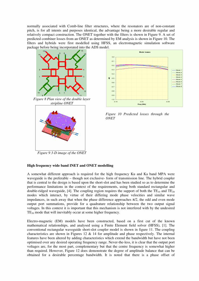
normally associated with Comb-line filter structures, where the resonators are of non-constant pitch, is for all intents and purposes identical, the advantage being a more desirable regular and relatively compact construction. The ONET together with the filters is shown in Figure 9. A set of predicted combiner losses from an ONET as determined by EM analysis is shown in Figure 10. The filters and hybrids were first modelled using HFSS, an electromagnetic simulation software package before being incorporated into the ADS model.
Figure 8 Plan view of the double layer
stripline ONET
Figure 9 3-D image of the ONET
Mode losses
-1.0
-0.9
-0.8
-0.7
-0.6
-0.5
-0.4
-0.3
-0.2
-0.1
0.0
2.15 2.20 2.25
Freq (GHz)
dB
Mode 1
Mode 2
Mode 3
Mode 4
Mode 5
Mode 6
Mode 7
Mode 8
Figure 10 Predicted losses through the ONET
High frequency wide band INET and ONET modelling
A somewhat different approach is required for the high frequency Ku and Ka band MPA were waveguide is the preferable – though not exclusive- form of transmission line. The hybrid coupler that is central to the design is based upon the short-slot and has been studied so as to determine the performance limitations in the context of the requirements, using both standard rectangular and double-ridged waveguide, [4]. The coupling region requires the support of both the TE10 and TE20 modes which interact, by virtue of their differing mode phase velocities and similar wave impedances, in such away that when the phase difference approaches π/2, the odd and even mode output port summations, provide for a quadrature relationship between the two output signal voltages. In this context it is important that this mechanism is not interfered with by the undesired TE30 mode that will inevitably occur at some higher frequency. Electro-magnetic (EM) models have been constructed, based on a first cut of the known mathematical relationships, and analysed using a Finite Element field solver (HFSS), [1]. The conventional rectangular waveguide short-slot coupler model is shown in figure 11. The coupling characteristics are shown in Figures 12 & 14 for amplitude and phase respectively. The internal features have been altered by adding characteristics which extend the bandwidth but have not been optimised over any desired operating frequency range. Never-the-less, it is clear that the output port voltages are, for the most part, complementary but that the centre frequency is somewhat higher than required. However, Figure 12 does demonstrate the degree of amplitude balance that can be obtained for a desirable percentage bandwidth. It is noted that there is a phase offset of
1
2
3
4
5
6
7
8
9 10
11
12
13
14
15
16

approximately 1.5° in the differential result that is accountable by a cumulative numerical error within the FE mesh where there is a cascade of at least 100 cells in the longitudinal direction. A greater mechanical refinement is necessary to reduce this problem implying a much greater solution time. This error is not expected to affect the differential data produced here to any significant degree. An alternative E-plane hybrid is shown in figure 13. The final 8 x8 ONET or INET is shown in figure 15.
Figure 11 Transparent view of WR75 H-
plane wideband hybrid
Figure12 H-plane wideband coupler results
Figure 13 E-plane Wideband Hybrid
coupler
Figure 14 E-plane Wideband Hybrid
coupler results
Figure 15 H-plane ka band 8x8 ONET
combiner
MPA Modelling The MPA itself has been modelled using the Agilent Advanced Design System (ADS) software. Theoretical models were developed for both 4 and 8-way MPAs that incorporated INETs, coaxial cables, amplifiers and ONETs as shown in Figure 16 for the case of an eight way design. A typical

set of output signals from the MPA in which one signal is shown with 7 leakage signals is shown in Figure 17. There is a predicted MPA isolation of 36 dB. The RF systems model gave rise to a mechanical model that incorporated all the equipment, allowing for the correct lengths of coaxial cables and thermal dissipation fins under the amplifiers.
INET_Sband_duroid_3X68
9
10
11
12
13
14
15
16
1
2
3
4
5
6
7
8
amp_switch_emp_uX44
8
7
6
5
1
2
3
4
amp_switch_emp_lX45
8
7
6
5
1
2
3
4
8x8_ONET_sbandX1
9
10
11
12
13
14
15
16
1
2
3
4
5
6
7
8
Filters_sbandX54
9
10
11
12
13
14
15
16
1
2
3
4
5
6
7
8
cable_block_Micro_CoaxX57
9
10
11
12
13
14
15
16
1
2
3
4
5
6
7
8
cable_block_GoreX56
9
10
11
12
13
14
15
16
1
2
3
4
5
6
7
8
Figure 16 The ADS model of the MPA
2.175E9 2.180E9 2.185E9 2.190E9 2.195E92.170E9 2.200E9
-60
-40
-20
0
-80
20
Frequency (GHz)
dBm
Figure 17 Predicted output signal levels of the MPA
MPA optimisation In order to provide a good isolation between the output ports of the MPA it is necessary to design and construct the MPA with the minimum of phase and amplitude errors. Notwithstanding this requirement there will be a residual phase and amplitude error caused mainly by the various cables that link the amplifiers to the Butler matrices via a series of switches for redundant amplifiers. A model of the MPA was created using Matlab based upon that shown in equation 4, this was then used to minimise the phase and amplitude errors through the use of the phase and amplitude correcting abilities of the amplifiers. A genetic algorithm was the tool that was used to search for the set of amplitudes and phases that would give an acceptable isolation, [3] & [8]. Peak to mean ratio analysis
In any high power equipment used in space there is always the risk that multipaction breakdown will occur. Since such breakdown is usually fatal it is best avoided. Multipaction breakdown is most likely to occur in dielectric free regions where the electric field strength is high. Multipaction is a process in which a charged particle inside a gap in a vacuum environment, oscillates due to the influence of an externally applied oscillating electric field of large strength, and every time it hits the gap walls it causes other charged particles to be released. These secondary charged particles then oscillate due to the externally applied electric field and release more charged particles upon impacting the gap wall. Eventually, the process creates a spark, which is undesirable and usually causes damage. A typical example of a likely site for multipaction breakdown is shown in Figure 18 where an ill fitting support bead exposes part of a conductor carrying high power.
RF OUTPUTSMA
CHASSISWALL
ISOLATORO/P PIN STANDARD
PTFE WASHER
RESIDUALAIR GAP
RF OUTPUTSMA
CHASSISWALL
ISOLATORO/P PIN STANDARD
PTFE WASHER
RESIDUALAIR GAP
Figure 18 Isolator / Output SMA Connector interface
In practice the multipaction risk for this position would be essentially eliminated by fitting of a second thin PTFE packing washer to fill the gap. A vital technique in the estimation of the multipaction hazard is the peak-to-mean power ratio. The amplitude of a band limited QPSK signal is not constant and the peak-to-mean power ratio is a highly relevant design parameter. The peak-to-mean power ratio at the output port of one of the amplifiers and at one of the ONET output ports was evaluated for the circuit shown in Figure 16 by means of the Envelope Analysis package contained within ADS. All of the components within the MPA were assumed to be linear except for the eight amplifiers which were assumed to be identical but with a gain characteristic as shown in Figure 19. The small signal gain characteristic has been extended for convenience of the reader.
-50 -45 -40 -35 -30 -25 -2025
30
35
40
45Amplifier Gain Characteristic
Input Power [dBm]
Out
put P
ower
[dB
m]
Figure 19 Amplifier Gain Characteristic
The peak-to-mean ratios as a function of mean power level were calculated to be as shown in Figure 20. The calculation was carried out for the case in which the inputs are contiguous on a 200 kHz grid, the mean power fed into each of the MPA input ports is the same, but all the QPSK modulations are different. A study revealed that while the amplitude of the amplifier output was approximately Rayleigh distributed, the output of the MPA was approximately Gaussian. Both distributions are truncated with the onset of amplifier limiting. It is interesting to note that while the amplifier output port appears to be the most strained by the multiple inputs, amplifier limiting does have a mitigating effect. On the other hand limiting makes matters worse at the MPA output ports. Practical experience at Astrium supports these ADS predictions.

10 15 20 25 30 35 40 450
1
2
3
4
5
6
7
8
9Peak-To-Mean Ratio
Power Level [dBm]
dB
Amplifier Output Port
MPA Output Port
Amplifier Output Port
MPA Output Port
Figure 20 Peak-To-Mean Ratios
Non-linear MPA analysis Amplifiers are by their very nature non-linear devices, which when two or more signals are passed through and amplified will generate inter-modulation product signals. This effect is of no small importance as the amplifiers are designed to operate at or just below the 1dB compression level, [6]. Figure 21 shows a test bench for a 4x4 MPA and a single amplifier to analyze and compare the effect of inter-modulation products. In the example shown three signals are passed through the single amplifier and the MPA and the resulting inter-modulation product signals examined. The amplifier response displayed in figure 22, and shows the three amplified signals and their 3rd order inter-modulation products at -10 dB. However, when three signals are amplified by the MPA, the output ports display a number of inter-modulation signals at -20 dB with the notable absence of the 3rd order inter-modulation signals, figure 23. The 3rd order inter-modulation signals appear though at the fourth port at -14 dB with respect to the three amplified signals.
ONET_4_way_idealX9
5
6
7
8
1
2
3
4
amp_block_ka_4_idealX11
5
6
7
8
1
2
3
4
RR6
RR4
RR5
RR3
RR7
P_nTonePORT6
P_nTonePORT3Num=3
P_nTonePORT5
INET_4_way_idealX8
5
6
7
8
1
2
3
4
Figure21 Test bench for a 4x4 MPA to analyze and compare the effect of inter-modulation products

19 20 2118 22
35
40
45
30
50
freq, GHz
dBm
(v_o
ut)
Figure 22 The output from the single amplifier showing the 3 amplified signals and the three 3rd order inter-modulation product signals
19 20 2118 22
20
40
0
60
freq, GHz
dBm
(v_o
ut1)
Figure 23 The output from the 4-way MPA showing one of the 3 amplified signals and the remaining inter-modulation product signals
19 20 2118 22
40
30
50
freq, GHz
dBm
(v_o
ut4)
Figure 24 The output from the 4th output port of the 4-way MPA showing the three 3rd order inter-modulation product signals

Conclusion This paper has described some of the RF modelling work that has been performed at Astrium on the subject of Multiport Power Amplifiers. It has described the components of the MPA and the mathematical modelling tools used in their analyses. Work continues on this subject and it is hoped to report on further developments in the future.
References [1] Developments in High Power Hybrid Output Networks, G R Cobb, ESA Microwave Technology and Techniques Workshop- Enabling Future Space Systems, ESTEC 2006 [2] Design of a multi-port amplifier beam forming network for a mobile communications antenna. P.James, J. Lowdell, S.V. Potter, G. Cobb, M. Walden & R. Hopper. EuCap Nice 2006. [3] Optimization of a Multi-port Amplifier Using a Least Squares Evolutionary Relaxation Method. P. James. EuMW Manchester 2006. [4]. ‘The Short-Slot Hybrid Junction.’ H. J. Riblet, Proceedings of the I.R.E., Vol. 40, February 1952. [5]’Matrix Amplifiers for Communications Satellite Applications’, J.S Joshi, Electronic and Communications Engineering Journal, Dec 1991. [6]’Nonlinear Distortion Analysis of a Multiport Amplifier’, M. Tanaka and Y. Suzuki, 22nd AIAA International Communications Satellite Systems Conference, May 2004. [7] ‘Advanced Payload for Multibeam Satellite that supports High Data Rate Broadband Global Area Network’, S. Curtis et al, AIAA, 2005 [8] ‘Optimised Multiport Amplifiers for Wideband Multi-beam Satellites’, Alan Couchman, Daryl Jones, 24th AIAA ICSSC, San Diego, 2006 [9] ‘Agilent ADS online documentation’. http://eesof.tm.agilent.com/support/ Acknowledgement The authors would like to thank the European Space Agency for their assistance and advice through part of this Artes4 Wideband MPA study.