Embed Size (px)
Citation preview

Helsinki University of Technology Department of Electrical and Communications Engineering Espoo 2004
RF Micro-electro-mechanical devices for 0.8-2.5 GHz applications in mobile terminals
Heikki Nieminen
Dissertation for the degree of Doctor of Science in Technology to be presented with due permission of the Department of Electrical Engineering, Helsinki University of Technology (Espoo, Finland), for public examination and debate in Auditorium Leonardo at Innopoli (Tekniikantie 12, 02150 Espoo) on the 10th of December 2004, at 12 o’clock noon.
Helsinki University of Technology Department of Electrical and Communications Engineering Metrology Research Institute

Helsinki University of Technology Metrology Research Institute PL 3000 FIN-02015 HUT Finland Tel. +358 9 451 2268 Fax. +358 9 451 2222 © Heikki Nieminen ISBN 951-22-7352-7 Otamedia Oy Espoo 2004

HELSINKI UNIVERSITY OF TECHNOLOGYP.O. BOX 1000, FIN-02015 HUT
http://www.hut.fi
ABSTRACT OF DOCTORAL DISSERTATION
Author
Name of the dissertation
Date of manuscript Date of the dissertation
Monograph Article dissertation (summary + original articles)
Department
Laboratory
Field of research
Opponent(s)
Supervisor
(Instructor)
Abstract
Keywords
UDC Number of pages
ISBN (printed) ISBN (pdf)
ISBN (others) ISSN
Publisher
Print distribution
The dissertation can be read at http://lib.hut.fi/Diss/
Heikki Nieminen
RF Micro-electro-mechanical devices for 0.8-2.5 GHz applications in mobile terminals
15.11.2004 10.12.2004
Department of Electrical and Communications Engineering
Metrology Research Institute
Radio frequency micro-electro-mechanical systems (RF MEMS)
Professor Robert Plana
Professor Ilkka Tittonen
Doctor of Science (Tech) Tapani Ryhänen
This thesis presents a wide tuning range micro-electro-mechanical (MEM) capacitor. The two-gap MEM capacitor has a measured nominal capacitance of 1.58 pF and achieves a tuning range of 2.25:1 with parasitic capacitance. When all parasitic capacitance to the substrate are extracted the measured nominal capacitance is 1.15 pF and the tuning range is 2.71:1. The device is made of electroplated gold and has a Q of 66 at 1 GHz, and 53 at 2 GHz. In addition, a novel three-state capacitor is presented. Measured capacitance of the first, the second and the third state are 0.86 pF, 1.61 pF and 3.68 pF, respectively.A novel temperature-compensated two-state microelectromechanical (MEM) capacitor is presented. The principle to minimize temperature dependence is based on geometrical compensation and can be extended to other devices such as continuously tunable MEM capacitors. The compensation structure eliminates the effect of intrinsic and thermal stress on the device operation. This leads to a temperature-stable device without compromising the quality factor (Q) or the voltage behavior. The compensation structure increases the robustness of the devices, but does not require any modifications to the process. Measurement results verify that the OFF and ON capacitance change is less than 6% and the pull-in voltage is less than 5% when the temperature is varied from –30°C to +70°C. I addition to the temperature stability, the charging of the dielectric layer is studied and a new continuous reliability measurement set-up is presented.This thesis describes important design principles of electrostatically actuated MEM capacitors. Key design principles, such as temperature compensation, calculation of mechanical properties, and calculation of electrical properties of MEM capacitor are studied in detail. A new design principle that describes how pull-in and release voltage ratio is only dependent on up and down capacitance ratio and not on the mechanical properties such as a spring constant is also derived. In addition, it is shown how the RF signal affects the voltage behavior of the MEM capacitor. Two-state, three-state and continuously tunable MEM capacitors are designed and fabricated using presented design principles.Modeling, fabrication and analysis of a truly three-dimensional high-quality-factor toroidal inductor using polymer replication processes is presented. The critical dimensions are in the micrometer range, and the applied manufacturing method is based on the polymer replication. Electrical measurements show that the inductor with an inductance of 6.0 nH exhibits a Q of 37 at 1GHz and a peak quality factor of 50 at a frequency of 3 GHz. Furthermore, the applied manufacturing technique can be extended to become a flexible packaging platform.
RF MEMS, Micro-electro-mechanical capacitor, micro-replicated RF toroidal inductor
951-22-7352-7 951-22-7353-5
Helsinki University of Technology


Contents
Acknowledgment 1 List of publications 3 Author’s contribution 5 1. Introduction 7 2. MEMS devices in RF systems 9 2.1 Possible applications . . . . . . . . . . . . . . . . . . . . . . . . . . . . . 9 2.2 Power amplifier matching network requirements . . . . . . . . . . . . 11 2.3 Structure and operation of RF MEM devices . . . . . . . . . . . . . . . 12 3. RF MEM capacitor 15 3.1 Process . . . . . . . . . . . . . . . . . . . . . . . . . . . . . . . . . . . . . . 15 3.2 Parallel plate actuator . . . . . . . . . . . . . . . . . . . . . . . . . . . . . 16 3.3 Electrical model and Q . . . . . . . . . . . . . . . . . . . . . . . . . . . . 19 3.4 Two-state MEM capacitor . . . . . . . . . . . . . . . . . . . . . . . . . . 23 3.4.1 Effect of ON and OFF capacitance on voltage behavior . . . . 23 3.4.2 Release voltage . . . . . . . . . . . . . . . . . . . . . . . . . . . . 24 3.4.3 Pull-in voltage . . . . . . . . . . . . . . . . . . . . . . . . . . . . 25 3.4.4 Hold-down voltage . . . . . . . . . . . . . . . . . . . . . . . . . . 25 3.5 Three-state MEM capacitor . . . . . . . . . . . . . . . . . . . . . . . . . 26 3.6 Continuously tunable MEM capacitor . . . . . . . . . . . . . . . . . . . 27 3.7 Temperature stability . . . . . . . . . . . . . . . . . . . . . . . . . . . . . 30 3.8 Reliability . . . . . . . . . . . . . . . . . . . . . . . . . . . . . . . . . . . . 34 4. Microreplicated RF toroidal inductor 39 4.1 RF inductor design . . . . . . . . . . . . . . . . . . . . . . . . . . . . . . 39 4.2 Microreplication . . . . . . . . . . . . . . . . . . . . . . . . . . . . . . . . 47 4.2.1 Substrate material . . . . . . . . . . . . . . . . . . . . . . . . . . . 47 4.2.2 Master fabrication . . . . . . . . . . . . . . . . . . . . . . . . . . . 47 4.2.3 Replication step and substrate moulding . . . . . . . . . . . . . . 47 4.2.4 Conductor lines . . . . . . . . . . . . . . . . . . . . . . . . . . . . 49 4.2.5 Assembly of inductor . . . . . . . . . . . . . . . . . . . . . . . . . 49 5. Conclusions 51

References 55 Paper reprints 63

Acknowledgment The work for this thesis has been carried out at Nokia Research Center, Helsinki, Finland during 1999-2004. I wish to express my gratitude to Tapani Ryhänen, the head of Microsystem Technologies Group, for providing me the opportunity to do this work. His encouragement convinced me to start the meticulous work of scientific writing. He is always a source of inspiration and provided guidance during the whole process. I would like to thank Vladimir Ermolov who has also guided my work during these five years. His Russian sense of humor brought many times a new angle to the situations that came up during this work. His comments regarding the publications have improved them immensely. Professor Ilkka Tittonen contributed to this thesis during the review process. I am grateful for his flexibility when I selected my post-doctoral studies and guidance during the final stages of this thesis. I am indebted to all the co-authors of the publications. We are tackling challenges that require a team effort to solve. Without the great team of Microsystems Technology Group in Nokia Research Center, Helsinki, Finland this work would not have been possible in this short period of time. Especially I would like to thank Kjell Nybergh and Jari Hyyryläinen for their contribution; Kjell for correcting the English language of all the publications and Jari for the help in building the transient capacitance measurement set-up. From the Electronics Laboratory I would like to thank Mikael Andersson and Panu Siukonen. They provided fast answers and helped in any question regarding the low and high frequency measurements. Timo Veijola from Helsinki University of Technology, Helsinki, Finland has contributed to one of the papers in this thesis. I have enjoyed working with him and especially would like to remember the good times we had, when visiting several microsystem-modeling conferences. Our Microsystems Technology Group has been an active one, Michel, Samuli, Jukka, Jussi, Antti, Kari, Hans-Otto, Markus, Marion, Ville, Martti, and others. You all have made working in Nokia Research Center an enjoyable experience, thank you. I wish to express my gratitude to our collaborators Tronic’s Microsystems, Grenoble, France and Åhmic, Uppsala, Sweden. I could not have hoped for better co-operation. Our relationship has been open and spontaneous. It has been the key to these successful results. Especially I would like to thank Marjorie Trzmiel and Christian Pisella from Tronic’s microsystems and Tomas Lindström from Åhmic. This work has required countless hours during weekends and evenings. I would like to thank my former room-mates Ville Torppa and Jani Päiväsaari, for their endurance and understanding for all the undone house works. Support that I got from them and from all the other members of team “Hurjat” is valued. In addition, I would like to thank all the members of “Hurjat” for providing relaxing alternatives to tedious work of science. Also I would like to acknowledge my gratitude to Helsingin Merimelojat
1

polo-team for their understanding when I skipped continuously practice sessions during writing of this thesis. When MEMS started to feel too small and I needed change, I wandered far and away. I never had to go alone. There were others who also yearned to see the wonders of the world. Jawa, Sumatra, Malesia, Singapore, Thailand, Vietnam, China, Macau, Hong Kong, Kuba, Dominican Republic, Costa Rica, Australia, New Zealand, with Jari Koponen and Toni Piponius I saw them all. Finally, my parents Aune and Erkki, sister Heta and Brother Mikko, thank you for everything.
2

List of publications This thesis is a compilation of the following papers published in international refereed journals: [P1] H. Nieminen, V. Ermolov, and T. Ryhänen, "Microelectromechanical capacitor
with wide tuning range", Electronics Letters, Vol. 37, pp. 1451-1452, 2001. [P2] H. Nieminen, V. Ermolov, K. Nybergh, S. Silanto, and T. Ryhänen,
"Microelectromechanical Capacitors for RF Applications", Journal of Micromechanics and Microengineering, Vol. 12, pp. 177-186, 2002.
[P3] V. Ermolov, T. Lindström, H. Nieminen, M. Olsson, M. Read, T. Ryhänen, S.
Silanto, and S. Uhrberg, “Microreplicated RF Toroidal Inductor”, IEEE Transactions on Microwave Theory and Techniques, Vol. 52, pp. 29-37, 2004.
[P4] H. Nieminen, V. Ermolov, S. Silanto, K. Nybergh, and T. Ryhänen, “Design of a
Temperature-Stable RF MEM Capacitor”, IEEE Journal of Microelectromechanical Systems, Vol. 13, pp. 705-714, 2004.
[P5] H. Nieminen, J. Hyyryläinen, T. Veijola, T. Ryhänen, and V. Ermolov,
“Transient Capacitance Measurement of MEM Capacitor”, Sensors and Actuators A, Vol. 117, pp. 267-272, 2005.
3

4

Author’s contribution Publications presented in this thesis are result from co-operation with Tronic’s Microsystems, Grenoble, France and Åhmic ab, Uppsala, Sweden. Tronic’s Microsystems manufactured the micro-electro-mechanical capacitors and Åhmic manufactured the toroidal inductor. All papers were primarily organized and written by the author. However, all the results presented in this thesis are result of teamwork. Especially work presented in [P3] has contribution from so many people that the authors are arranged in alphabetical order. Author carried out all the simulations, measurements, and analysis presented in this thesis except for the measurement and HFSS simulation of a transformer in Fig. 14 of [P3]. Tomas Lindström from Åhmic has written and drawn figures on the microreplication process presented in [P3] and in Chapter 4.2 of this thesis. All the novel structures presented in [P1], [P2], [P4], and [P5] are designed by the author. Author derived the dependence of pull-in and release voltage ratio on the up and the down state capacitance ratio and showed how a RF signal can affect the voltage behavior even if the RF signal is at higher frequency than the resonance frequency of the MEM structure [P2, P4]. Author also invented the novel three-state MEM capacitor presented in [P2]. The idea of the microreplicated toroidal inductor presented in [P3] was proposed by Tapani Ryhänen. Author is one of the main inventors of the novel temperature compensation principle and structure presented in [P4] and holds a patent [1] regarding this principle. Author constructed together with Jari Hyyryläinen from Nokia Research Center, Helsinki, Finland the novel measurement set-up for continuous reliability measurement of a MEM capacitor presented in [P5]. Paper [2] and [3] are not included in to this thesis because they are invited papers. Papers [4] and [5] were not included in this thesis in order to keep this thesis compact.
5

6

1. Introduction New functionality and miniaturization of existing architectures using re-configurable systems are required for the future wireless systems. Micro-electro-mechanical (MEM) radio frequency (RF) switches [6,7], tunable capacitors [P2], high Q inductors [P3], and resonators [8, 9] are the building blocks for new low loss, highly linear and re-configurable RF architectures. Some of these technologies are closing the maturity level required in a commercial product like the MEM switch, others like the MEM resonator still require several years of research. Analysis of current or in near future available components shows that one of the most potential places to use RF MEMS is in circuits that handle large RF power [10]. This means transmit (Tx) paths [11] and antennas. Possible applications are antenna switches, tuners [12, 13], switched filters [10, 14, 15], reconfigurable antennas [16, 17], low loss phase shifters [18, 19, 20], and phased antenna arrays. Power amplifier (PA) lines for multiple bands can be combined using MEM switches or capacitors to reduce size and cost when PA chips and output matching circuits are eliminated. This thesis presents design, measurements and analysis of novel components that can be used to create low loss, highly linear, and re-configurable matching networks. Two components are discussed in detail: MEM capacitor and micromachined toroidal inductor. Losses in the matching network mainly come from the inductors that have the lowest Q. Design principles, measurement, and analysis of novel technology to create high Q toroidal inductors are presented. MEM capacitor designs are divided into three categories: two-state, three-state, and continuously tunable MEM capacitors. Two common problems are identified, lack of temperature stability and charging of the dielectric layer. To compensate the temperature dependence of the MEM capacitor a novel method is presented here. This method is not restricted to any fabrication process and it reduces effect of all kinds of stress, not only temperature related, on the suspended structure. Changes on the MEM capacitor behavior due to the charging of the dielectric layer are also analyzed. Based on the analysis, a novel continuous reliability measurement set-up is demonstrated. This set-up accurately shows changes in a MEM capacitor behavior that have not been previously demonstrated. Second type of MEM capacitor presented in this thesis is a novel three-state MEM capacitor concept. This concept allows third stable capacitance state to be added into the traditional two-state MEM capacitor without an increase in the device area. Third category of MEM capacitors that is discussed is the continuously tunable capacitor.
7

8

2. MEMS in RF systems There will be many transmit (Tx) and receive (Rx) paths in future mobile devices: global system for mobile communications (GSM) 850/900/1800/1900 MHz, code Division Multiple Access cellular technology (CDMA) 850/1900 MHz, wideband CDMA (W-CDMA) 850/1900/2000 MHz, Bluetooth (BT) 2400 MHz, wireless local area network (WLAN) 2400 MHz, and ultra wideband radio (UWB). In addition to these, there are also some receive-only-paths like Galileo positioning system, global positioning system (GPS), and digital video broadcasting (DVB-H). Direct consequence of these numerous Rx and Tx paths is that the number and/or complexity of antennas is increasing. Re-configurability of a RF system using MEM switches, two-state capacitors or continuously tunable capacitors can reduce the number of components and the size of the overall architecture. For instance, re-configurability of RF system can decrease number of components as shown in case of Rockwell Collins filter [10]. In that particular case, two MEM varactors replace 16 silicon varactor diodes due to their capability to withstand large AC voltage and current. 2.1 Possible applications MEM devices have naturally some limitations:
1) MEMS need to be nearly hermetically packaged to protect devices from moisture. Therefore the integration of MEMS into IC is demanding. Packaging also increases price and size of the RF MEMS component.
2) Speed of MEM device is related to mechanical resonance frequency. This means that MEM switches and capacitors typically are slow. Switching times normally are in the order of 10-100 µs.
Due to aforementioned facts, there must be clear benefits that justify use of MEMS. Analysis of current or in near future available components shows that MEM devices give great benefits when used is in places where there is large RF power [10]. This means Tx paths and antennas. The reasons are:
1) MEMS stands high RF power if properly designed: MEM switchable/tunable capacitor power handling is limited either by the dielectric charging and/or self-actuation [10, 21]. In addition, MEM capacitor stands well hot switching. MEM ohmic contact switches are more susceptible to damage, but significant improvement has happened [7, 22].
2) Good linearity: IP3 is usually over 60 dBm [22].
3) Low losses: Capacitors can have Q over 200 at 2.4 GHz and switches can have loss less than 0.15 dB at 2.4 GHz [7].
9
Fig. 1 shows some of the possible applications for MEM switches and capacitors in mobile phone front-end, switched filter bank, and phased antenna array.
SPDT
Tunable network
re-configurable antenna
Tunable network
PA
LNA
(a)
1P4T
Filter
1P4T
(b)
φ
φ
φ
φ
T/R
T/R
T/R
T/R
T/R
T/R
(c)
Fig. 1. Some of the possible applications for MEM switches and capacitors in (a) mobile phone front-end including re-configurable antenna, (b) switched filter bank, and (c) phased antenna array where one T/R module stage can be removed due to small losses in RF MEM phase shifter.
10

2.2 Power amplifier matching network requirements Especially promising application for RF MEMS is a tunable PA output matching network. RF MEM components can help to reduce losses in PA matching network. PA lines for multiple RF bands can be combined using MEM switches or capacitors to reduce size and cost when PA chips and output matching networks are eliminated [11]. In addition, power can be saved changing the PA output matching to correspond to the PA output impedance that changes with output power [3]. Typically the mobile phone PA matching network is optimized at the maximum output level. When the PA output power is reduced the output impedance of the PA changes also. This means that reflections from the matching network increase and power is lost. There are several solutions to reduce reflections. One solution is to use DC/DC converter to change bias of the PA. However, high efficiency DC/DC converters are bulky and expensive. Second solution is to adapt the matching network to different PA power levels. Simulation shows that PA optimized for maximum output of 34 dBm consumes 377 mA at 23.4 dBm. If the PA output matching circuit is reconfigured using MEM capacitor so that reflections are minimized at 23.4 dBm, the current consumption is only 140 mA [3]. Third possibility is to make several switchable PA lines that are optimized to different power levels [23]. Fig. 2 shows a simple PA output matching network that can be used to match two PA output impedance levels.
Fig. 2. PA output matching circuit that can be used to match several PA output impedances to minimize reflections.
11

Fig. 2 shows that inductors and tunable/switchable capacitors are required in the re-configurable PA output matching network. Table I gives some reference values for these components in mobile phone applications. Table I is not a specification for the matching network components.
TABLE I
REFERENCE VALUES FOR PA MATCHING NETWORK COMPONENTS
Device Inductor Tunable/switchable capacitor
Typical values 1-6 nH 0.3-2 pF / 5-20 pF Losses Q as high as possible Q as high as possible Power handling 37 dBm 37 dBm Linearity > 60 dBm > 60 dBm Switching speed <100 µs minimum, many
applications <10 µs Hot switching Yes
Stability (Temperature –30 °C to +70 °C, aging 10 years)
< 2% inductance variation < 5% capacitance variation
Reliability 1012 cycles
2.3 Structure and operation of RF MEM devices Typically inductors have the lowest quality factor (Q) of the matching circuit components. Therefore high Q inductors are required in the PA output matching network. A concept picture of novel high-Q three-dimensional (3D) toroidal inductor in a plastic substrate is shown in Fig. 3. Inductor is fabricated from the micromolded plastic structure in two halves. The plastic microstructure is fabricated first using so-called micro-replication technology [24-26] and after that metal is deposited and etched using standard IC process steps. The two halves are connected together at the wafer level at the end of the process.
12

(a) (b) Fig. 3. (a) Half of the microreplicated toroidal inductor. (b) Assembled microreplicated toroidal inductor from ref. [P3].
Fig. 4 shows a simplified MEM capacitor structure. In the MEM capacitor, a thin and wide electrode that is typically made from metal, is suspended (fixed from both ends) in air over a fixed electrode that is also typically made from metal. When the voltage is applied between the electrodes the electrostatic force displaces the top electrode down towards the bottom one and the capacitance between the electrodes changes. An opposing mechanical force is created, as the structure bends due to displacement, balancing the electrostatic force.
Mechanical force is linear as a function of the displacement, but the electrostatic force is non-linear. Therefore when applied voltage reaches a certain threshold value (Vpull-in), the mechanical force can no longer balance the electrostatic force and the top electrode abruptly falls to the bottom electrode. This phenomenon is called pull-in. If the magnitude of voltage is then reduced, the upper electrode releases back up, but typically at a much lower voltage than Vpull-in. This creates hysteretic voltage behaviour.
13

Signal line
Substrate
Ground
Movable electrode
Perforation holes to remove sacrificial layer
Dielectric layer on top of fixed electrode
Electroplated Anchoring
Fig. 4. Structural drawing of (fixed-fixed beam) MEM capacitor.
14

3. RF MEM capacitor 3.1 Process Several variations of the initially defined process were used to fabricate the MEM capacitors [P2]. In order to reduce cost, the devices were first fabricated on low resistivity silicon (~ 1 Ω-cm). Because the low resistivity substrate causes losses, it was selectively removed under the fixed electrodes as shown in Fig. 5. However, the substrate losses were still rather high and the dielectric membrane supporting the MEM capacitor proved to be rather unreliable so in the end the low resistive substrate was replaced by high resistive silicon and backside etching was not done.
signal electrodecontrol
electrode
Back side etched
V1C1
Electroplated anchoring
SiO2
Silicon
SiNx
SiO2
Metal 1SiNx
Thick Metal
Metal 2
Moving electrode
Fig. 5. cross-section view of the capacitor structure with separate control and signal electrodes and two different air gaps from ref. [P2]. Structural material of the devices was chosen to be gold due to its high conductivity and due to fabrication issues. Since there was not available a MEMS fabrication process that could be tailored based on the design needs, a new process was developed by Tronic's Microsystems, Grenoble, France. The fabrication process uses gold to form both the fixed electrodes (Metal 1) as well as the suspended electrodes (Metal 2 and thick electroplated metal). On top of the Metal 1 layer a silicon nitride dielectric layer (εr=7.5) was formed. This isolates the suspended electrode from the fixed electrodes in the case of pull-in. The air gap was realized using a polymer as a sacrificial material. In order to remove the sacrificial material from underneath the metal 2 and 3, perforation holes were made to the suspended electrodes. The perforation holes in
15

metal 2 were 4 × 4 µm2 in size with 12 µm spacing. Metal 3 perforation holes were 10 × 10 µm2 in size with 20 µm spacing. The two-gap structures were realized using an additional oxide layer under selected fixed electrodes and by planarizing the polymer before the deposition of Metal 2 and metal 3. Fig. 5 shows a simplified cross-section view of the MEM capacitor structure with separate control and signal electrodes and two different air gaps. Table II shows the layer thicknesses used in the device.
TABLE II
LAYER THICKNESSES
Layer Thickness [µm] Silicon dioxide 1 Silicon nitride 0.5 Step silicon dioxide 1 Metal 1 (gold) 1 Dielectric layer (SiNx) 0.1 Sacrificial layer (Polymer) 0.5/1.5 Metal 2 (gold) 0.5 Metal 3 (gold) 10
3.2 Parallel plate actuator A MEM capacitor usually consists of two parallel plates: one plate is fixed and the other one is suspended using a mechanical spring with a spring constant k so that the control voltage V can vary the gap between the plates. The functional model of the one-gap MEM capacitor is shown in Fig. 6. td is the thickness of the dielectric layer on top of the lower electrode, t0 is the air gap between the electrodes under zero control voltage, and t is the air gap when the control voltage is applied. When the suspended electrode moves, air-damping that is related to the speed slows the movement. The dynamic response of the parallel plate actuator is [27] ee Fkttbtm =++ &&& , (1) where me is the effective mass, b is the damping coefficient, Fe is an external force, t is the displacement, t and t are the first and second time derivative of the displacement, respectively.
& &&
16

Spring kGas damping
V C(V)
t dt 0t
Suspended electrode
Signal electrode Fig.6. Functional model of one-gap MEM capacitor from ref. [P2]. Our simple model assumes that whole mass of the moving structure is accelerated at the same amount. If the moving structure is experiencing elastic deformation (bending) different parts of it are experiencing different accelerations. For instance in the case of fixed-fixed beam the center of the beam experiences larger acceleration than the ends of the beam. To take this into account a concept of effective mass (me) of the electrode is introduced. Usually the effective mass is calculated using commercial mechanical modeling tools like finite element method (FEM) program. The gas-damping coefficient for circular membrane with holes is experimentally derived [28] to be
⎟⎟⎠
⎞⎜⎜⎝
⎛−−−=
83
4)ln(
8212 2
30
2 ppptA
Nb µ
π, (2)
where N is the total number of holes, A is the membrane area, p is the fraction of the open area on the membrane, and µ is the coefficient of viscosity. The equation for the viscosity [29] is RT21792.0 πρλµ = , (3) where R is the specific gas constant, ρ is the gas density, λ is the mean free path, and T is the temperature. The mean free path, the distance covered by the molecule between successive collisions, is [29]
σπ
λN2
1= , (4)
17

where σ is the diameter of the gas molecule and N is the number density of the gas. Number density is
0m
N ρ= , (5)
where m0 is the mass of single gas molecule. The spring constants k for different structures evaluated in this thesis are calculated in [30]. For the temperature compensated capacitor spring constant of cantilever beam can be used
3
1 4⎟⎠⎞
⎜⎝⎛=
LtEwk , (6)
where w is beam width, t is beam thickness, L is length of the beam, and E is Young’s modulus. Spring constant of fixed-fixed type MEM capacitor that takes into account width of the lower electrode underneath the suspended electrode is [30]
( ) ( ) ( ) 114208
132 23
3
2 −+−⎟⎠⎞
⎜⎝⎛=
LxLxLxLtEwk , (7)
where
2
2wLx
−= . (8)
w2 is the width of the lower electrode. MEM bridge capacitor that has two control electrodes underneath the suspended electrode as shown in Fig. 5 has a spring constant [30]
( )2
3
3 114
LxLxLtEwk
−⎟⎠⎞
⎜⎝⎛= , (9)
where x is the width of the control electrode. Residual stress σ in the beam increases the effective spring constant in one and two electrode case [30]
LxL
twk231)1(82 −
−=′′ νσ (10)
18
and
LxL
twk−
−=′′1
1)1(43 νσ , (11)
respectively. Here ν is the Poisson’s ratio. The total spring constant for the fixed-fixed beam with one and two control electrodes is therefore 22 kk ′′+ and , respectively.
33 kk ′′+
The capacitance value can be controlled by the voltage difference or by controlling the charge on the capacitor plates. In case of the voltage control, the voltage difference attracts the suspended electrode towards the fixed electrode until equilibrium between the spring force and the electrical force is reached. Mathematically this can be formulated in a steady state situation as follows:
2
2202
0 )(221)(
ttAV
CVt
Fttkrd
re ε
εε+
=∂∂
−==− , (12)
where A is the area of the capacitor plates, V is the control voltage, εr is the effective dielectric constant of the dielectric layer on top of metal 1, and ε0 is the permittivity of vacuum. Since the spring force is a linear function of the air gap and the electric force is inversely proportional to the second power of the air gap, there exists a stable equilibrium point only when
r
dttt
ε332
0 −≥ . (13)
After this point pull-in happens and the suspended electrode collapses on top of the fixed electrode. If the control voltage is decreased, the suspended electrode remains in its pull-in state until some voltage level, the release voltage, is reached. The pull-in limits the theoretical continuous tuning range of the voltage controlled one-gap MEM capacitor to 50 %. 3.3 Electrical model and Q Typical goal in a capacitor design is to maximize the electrical Q for the device when the capacitance range is defined. In addition to that the maximum control voltage for the MEM capacitor might be defined. Here the MEM capacitor Q is defined as
19

)()()(
fRfXfQ
m
m= , (14)
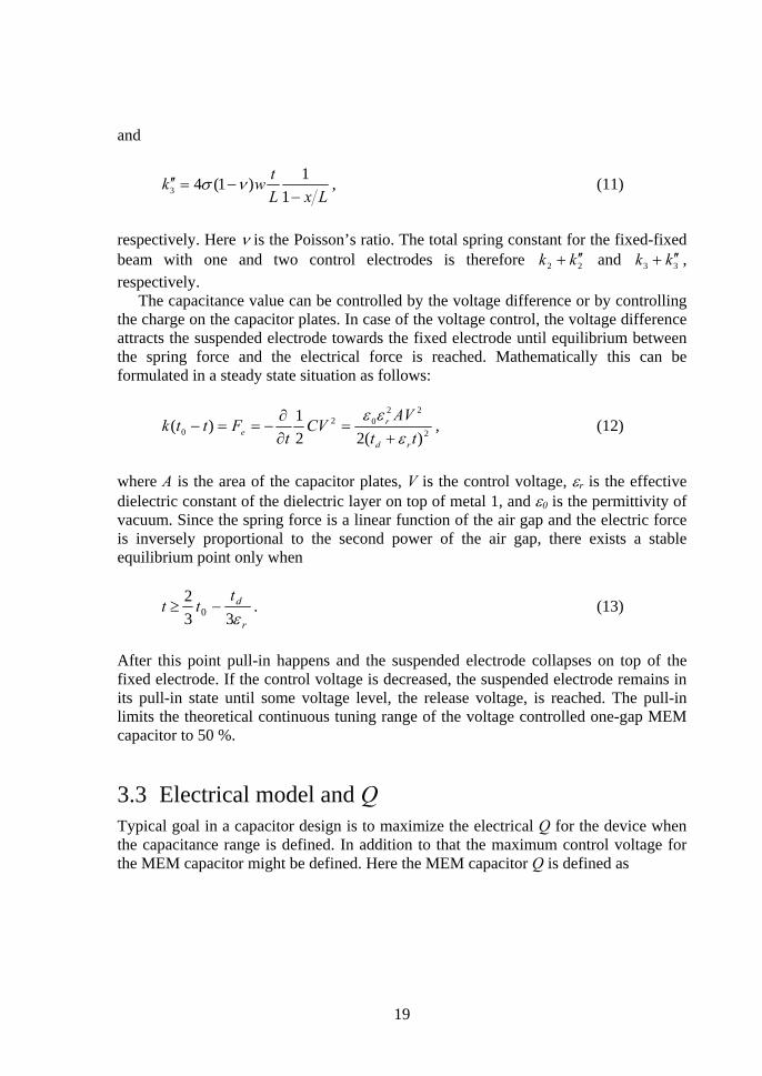
where f is the operating frequency, and Rm(f) and Xm(f) are the real and imaginary part of the capacitor impedance (Z), respectively. Fig. 7 shows a simple capacitor equivalent circuit. This circuit is used to demonstrate how different parasitics affect Q. In the figure CMEM is the capacitance of the device, Rs is the series resistance, Ls is the parasitic series inductance, Csub is the parallel parasitic capacitance to substrate, Rsub is the substrate resistance, and Rp is the parallel resistance due to the leakage current between signal and ground electrode through surface of the dielectric.
Rsub=200kΩ
Ls=50pH
CMEM=1pF
Rp=100kΩ
Rs=0.2Ω
Csub=0.4pF
Fig. 7. Simple equivalent circuit of the MEM capacitor. In integrated circuits, a small leakage current path along the free surface of the dielectric layer is always present connecting the signal line to the ground. Typically a parallel resistance between 50kΩ-5MΩ can be used to model this leakage current path. Fig. 8 shows the influence of this leakage current on the Q of the capacitor. Figure indicates that at low frequencies the Q has stronger dependence on leakage current. This is to be expected since the impedance of the capacitor decreases with the frequency. Therefore the current that goes through the capacitor increases and the current that goes through the leakage path decreases with the frequency.
20
0
100
200
300
400
500
600
0 2 4 6
Frequency [GHz]
Q
8
R p =∞
R p
0.5R p
0.25R p0.1R p
Fig. 8. Simulated effect of parallel resistance Rp on capacitor Q value. Equivalent circuit parameters as in Fig. 7, except Csub=0, Rsub=0. Series resistance is expected to behave as f . In addition to leakage current trough the surface of the dielectric, part of the RF signal also couples to ground through the substrate. In case of the capacitor the dominating coupling mechanism is capacitive coupling. Fig. 9 shows how the substrate resistance influences the Q of the capacitor. Since this is leakage path in parallel to the MEM capacitor and resistance dominates the impedance of the leakage path, the Q behavior is similar to Fig. 8. The impedance of this leakage path is naturally also dependent on Csub. Leakage current paths have large influence on the Q at low frequencies. On the other hand the series resistance of the MEM capacitor has major effect on the Q only at higher frequencies. Fig. 10 shows how series resistance Rs influences on Q. It should be noted that this behavior is opposite compared to the inductor Q. In case of an inductor the series resistance mainly affects the Q at low frequencies.
21

0
100
200
300
400
500
600
0 1 2 3 4 5 6 7 8
Frequency [GHz]
QR sub R sub = ∞
0.5R sub
0.25R sub
0.1R sub
Fig. 9. Simulated effect of substrate resistance Rsub on capacitor Q value. Equivalent circuit parameters as in Fig. 7, except Rp=0. Series resistance is expected to behave as f .
0
50
100
150
200
250
300
0 1 2 3 4 5 6 7 8
Frequency [GHz]
Q
R s
2R s
3R s
4R s
Fig. 10. Simulated effect of series resistance Rs on capacitor Q value. Equivalent circuit parameters as in Fig. 7. Series resistance is expected to behave as f .
22

3.4 Two-state MEM capacitor RF signal can change the MEM capacitor value as is presented in [P2]. To avoid this, the pull-in phenomenon and hysteretic voltage behavior can be used to create a MEM capacitor that has several stable states. The capacitance value in one state does not change due to the small voltage changes. However, when the control voltage exceeds certain threshold value, capacitor abruptly changes to the next state. For instance, a two state capacitor can be designed so that it has certain voltage region, for instance from 0 to 0.5Vpull-in, where capacitance stays approximately constant in value COFF. When threshold (pull-in voltage) is passed, the capacitance abruptly changes to second stable value CON that is defined by the dielectric thickness and does not change due to the small voltage variations. Therefore this design can be operated as planned even under relatively large RF power. Design principles of the two-state capacitor are discussed next.
3.4.1 Effect of ON and OFF capacitance on voltage behavior Two-state MEM capacitor design starts from the definition of the OFF (COFF) and ON capacitance (CON). It is derived in [P2] and [P4] that COFF/CON capacitance ratio defines the pull-in and release voltage (Vrelease) ratio. Vrelease is defined as the smallest voltage that keeps the capacitor in the ON state. It is known that [30]
3
220
32
32
OFFinpull C
kAV
ε⎟⎠⎞
⎜⎝⎛=− (15)
and
2002 2
ONrelease C
AtkV
ε= . (16)
The ratio between Vrelease and Vpull-in follows from (15) and (16) [P4]
⎟⎟⎠
⎞⎜⎜⎝
⎛+
⎟⎠⎞
⎜⎝⎛=
− 0
03
2
2
2
2 223
ttt
CC
VV
rd
r
ON
OFF
inpull
release
εε
(17)
where td is the dielectric layer thickness. If the ON and OFF capacitance ratio is defined as
ON
OFF
CC
=α (18)
23

(17) becomes
)1(223 2
3
αα −⎟⎠⎞
⎜⎝⎛=
−inpull
release
VV
, (19)
Since the capacitance ratio in practice defines td and t0, the design parameter that is free for the control voltage tuning is spring constant k. Here, the spring force is assumed to be linear. It must be kept in mind that whenever large deflection occurs, this assumption is no longer valid. As a result, estimation for the pull-in voltage (15) is more accurate than estimation for the release voltage (16). 3.4.2 Release voltage
Assuming that the RF voltage signal is sinusoidal (ûRF sinωt), it generates a force [P2] that is equivalent to that caused by a DC voltage (VRF) over the capacitor according to
2
ˆRFRF
uV = . (20)
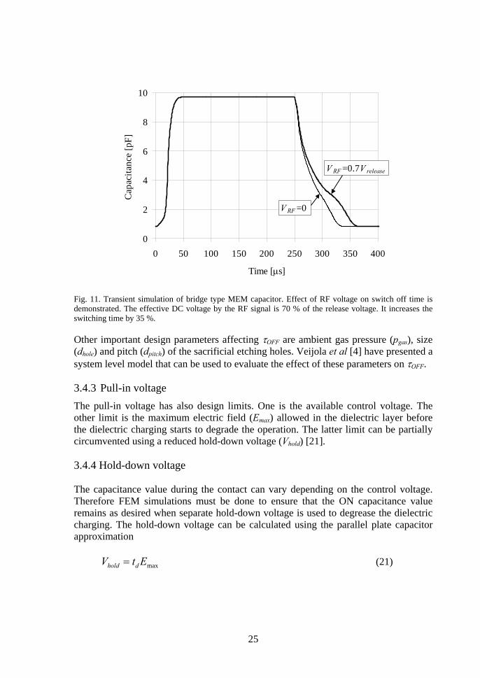
The Vrelease voltage of the device must be larger than the VRF generated by the RF voltage signal. Only in that case can the MEM capacitor go from the ON state to the OFF state when the control voltage is switched to zero but the RF voltage signal is still over the device. This is one of the design constraints for Vrelease. However, ON-to-OFF-state switching speed (τOFF) sets an even higher limit for the release voltage. The RF voltage signal over the MEM capacitor causes a force that tries to pull the suspended membrane down. Therefore, when the device is switched from the ON state to the OFF state, the RF voltage signal increases τOFF. This is demonstrated in Fig. 11. The effective DC voltage by the RF signal (VRF) is 70 % of the release voltage. It increases the switching time by 35 %. Simulation is done using same Aplac model of bridge type MEM capacitor as is described in [P5, 4]. When the VRF reaches Vrelease, τOFF goes to infinity and switch stays down. Measurements presented in [P5] show that the dielectric charging causes also an effective DC voltage between the electrodes that can slow the switching speed. However, results from the [P5] show that the charging saturates to a value defined by the electric field over the dielectric layer. Therefore after the maximum-trapped charge as a function of electrical field is defined using the reliability testing, it becomes just one more design constraint.
24
0
2
4
6
8
10
0 50 100 150 200 250 300 350 400
Time [µs]
Cap
acita
nce
[pF]
V RF =0
V RF =0.7V release
Fig. 11. Transient simulation of bridge type MEM capacitor. Effect of RF voltage on switch off time is demonstrated. The effective DC voltage by the RF signal is 70 % of the release voltage. It increases the switching time by 35 %. Other important design parameters affecting τOFF are ambient gas pressure (pgas), size (dhole) and pitch (dpitch) of the sacrificial etching holes. Veijola et al [4] have presented a system level model that can be used to evaluate the effect of these parameters on τOFF. 3.4.3 Pull-in voltage The pull-in voltage has also design limits. One is the available control voltage. The other limit is the maximum electric field (Emax) allowed in the dielectric layer before the dielectric charging starts to degrade the operation. The latter limit can be partially circumvented using a reduced hold-down voltage (Vhold) [21]. 3.4.4 Hold-down voltage The capacitance value during the contact can vary depending on the control voltage. Therefore FEM simulations must be done to ensure that the ON capacitance value remains as desired when separate hold-down voltage is used to degrease the dielectric charging. The hold-down voltage can be calculated using the parallel plate capacitor approximation (21) maxEtV dhold =
25

where maximum electric field (Emax) is defined by the electrical reliability testing and td is defined by the required capacitance density. This in turn limits the maximum ON capacitance density. 3.5 Three-state MEM capacitor The two-state capacitor concept can be developed further in to novel three-state capacitor presented in [P2]. The advantage of the concept is one more stable capacitance state without increasing the device area. Fig. 12 shows the operational concept of the three-state capacitor.
SiO2
Silicon
SiNx
SiO2
Metal 1SiNx
Thick MetalMetal 2
Fig. 12. Operation principle of the three-state capacitor from ref. [P2]. Designing the three-state MEM capacitor is simple. Two-state MEM capacitor design principle is used and then a ridge is added into the middle of the lower electrode. This ridge creates the third (middle) capacitance state. Fig. 13 presents measurement results of the three-state MEM capacitor. See also ref. [P2]. University of Michigan has also published a three-state MEM capacitor in [31]. However, in [31] the measurement results show rather small voltage region for the middle capacitance state and the voltage behavior back from high state to low state is not shown. It can be speculated whether [31] can return from high state to middle state is as is shown in Fig. 13 measurement results.
26

Fig. 13. Measured capacitance as a function of voltage of the three-state MEM capacitor from ref. [P2].
3.6 Continuously tunable MEM capacitor The pull-in limits the theoretical continuous tuning range of the voltage controlled one-gap MEM capacitor to 50 %. One way to go around the pull-in phenomenon is to use separate control and signal electrodes [P1, P2]. In this case the air gap between the control electrode and the suspended electrode can be made larger than the gap between the signal electrode and the suspended electrode. Fig. 14 shows the functional model of the two-gap MEM capacitor structure. Distance t2 in the figure is the difference between signal electrode air gap and the control electrode air gap. If for the initial air-gap t0 between the signal electrode and suspended electrode the relation
r
dttt
ε221
20 +≤ (22)
holds true, then pull-in due to the control voltage does not occur before the suspended electrode touches the signal electrode. In this case, the capacitance due to the dielectric layer defines the theoretical maximum tuning range.
27

Spring kGas damping
C(V)
Control electrode
Signal electrode
Suspended electrode
V
t dt 0t
t 2
Fig. 14. Functional model of two-gap MEM capacitor from ref. [P2]. Several research groups have demonstrated continuously tunable MEM capacitors. Table III summarizes the published results. Usually the two main parameters, Q and the tuning range, are used to describe the operation of the capacitor. However, comparison of the different devices is difficult since the absolute capacitances are not same and the Q is measured at different frequencies.
TABLE III
SUMMARY OF CONTINUOUSLY TUNABLE MEM CAPACITORS
Authors Year Tuning range % Control [V] Q Rijks et al [32] 2004 0.2-0.72pF 1-1.7pF - 0-20 150 at 1 GHz De Coster et al [33] 2003 0.07-0.255 pF 264 0-21 - Tsai et al [34] 2003 1.78-3.88 pF 118 -10+10 - Altug and Fedder [35] 2003 0.042-0.148 pF 252 0-12 52 at 1.5 GHz Gallant and Wood [36] 2002 0.7-3.6 pF 414 0-12 - Ionis et al [37] 2002 1.9-2.9pF 3.6-6.7pF - 0-13 17 at 1.5 GHz Borwick et al [38] 2002 1.4-11.9 pF 750 0-8 30 at 2.25 GHz Ionis et al [39] 2001 3.1-4.6 pF 46 0-35 6.5 at 1.5 GHz Park et al [40] 2001 0.1-0.31 pF 210 0-6 210 at 1 GHz Nieminen at al [P1, P2] 2001 1.58-3.55 pF 125 0-17.7 53 at 2 GHz Zuo et al [41] 2000 ~0.45-0.76 pF 70 ~0-18 - J-B. Yoon and C. Nguyen [42]
2000 1.14-1.6 pF 40 0-10 218 at 1 GHz
Yao et al [43] 2000 1.3-6 pF 362 0-6 40 at 1.5 GHz Feng et al [44] 1999 0.102-0.2 pF 100 - 256 at 1 GHz Dec et al [y45] 1998 3.4-6.4 pF 87 0-4.4 15.4 at 1GHz Young and Boser [46] 1996 2.04-2.35 pF 15 0-3 60 at 1 GHz
Therefore some kind of normalization is required to compare the results. If the Q of the capacitor is assumed to have very simple dependence on frequency and capacitance
28

CRjfR
fXQω
1)()(
== . (23)
The Q can be normalized
norm
measured
norm
measurednormalized f
fC
CQQ = (24)
where Cnorm is 1 pF and fnorm is 1 GHz. Drawback of this normalization method is that it assumes that all devices have the same size. Fig. 15. shows normalized results from different research groups.
0
100
200
300
400
500
600
700
800
0 50 100 150 200 250 300
Normalized Q
Tuni
ng ra
nge
[%]
Rijks et al [32]
Altug and Fedder [35]
Ionis et al [37]
Borwick et al [38]
Ionis et al [39]
Park et al [40]
Nieminen at al [P1, P2]J-B. Yoon and C. Nguyen [42]
Yao et al [43]
Feng et al [44] Dec et al [45]
Young and Boser [46]
State of the art 1H/2004
Fig. 15. Summary of the tunable capacitor results from different research groups. The Q is normalized to frequency 1GHz and to capacitance 1pF. It is possible to make design compromises to improve the Q. For instance, increasing the initial air-gap increases the Q, but at the same time the capacitance density drops. Normalization of the Q shows how well the optimization between device capacitance density and Q has been done. When looking Fig. 15 it can be seen that there are a
29
couple of research results that clearly distinguish from the rest. Yoon and Nguyen [42], this doctoral thesis [P1,P2], and Borwick et al [38] present the state of the art results at the moment. Another way to increase the tuning range is to use charge control. In this case the equation between mechanical spring force and electrical force changes to
A
qCq
tCV
tttk
0
222
0 221
21)(
ε=
∂∂
=∂∂
−=− , (25)
where q is the charge pumped to the electrode. The force due to the charge is now independent of the gap and thus in the ideal case the charge control allows full control of the capacitor air gap. However, in reality the parallel parasitic capacitance limits the maximum control range and leakage currents make the control of the amount of charge difficult. Several research groups have demonstrated different voltage and charge control methods. Table IV compares the advantages and disadvantages of these methods.
TABLE IV
TUNABLE MEM CAPACITOR CONTROL METHODS FROM REF. [P2].
Method Advantages Disadvantages Charge control with IC control circuit [47]
Requires just slightly larger supply voltage than is the pull-in voltage of the capacitor [48]
Resetting consumes power, can be sensitive to leakage currents
Charge control using a coil [49]
Very low AC control signal Requires high Q coil
Two-gap capacitor structure [50]
Simple, separate control and signal electrodes
Large control voltage
Charge control using capacitive feedback [51]
Simple Large control voltage, can be sensitive to leakage currents
3.7 Temperature stability The MEM capacitor is often made of metal to minimize resistive losses. Substrate material is usually silicon, quartz or glass. These substrate materials usually have thermal expansion coefficient close to 3 ppm/K, but it can be tailored for some substrates. Most metals have thermal expansion coefficient over 14 ppm/K. This means that when temperature changes, substrate and capacitor made of metal expand or contract with a different rate. This causes thermal stress. Highly simplified estimation for thermal stress is ( ) TE SiAuAu ∆−= αασ , (26)
30
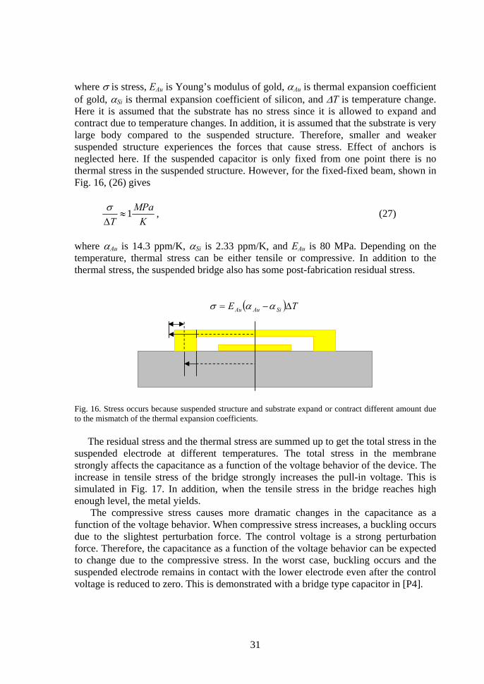
where σ is stress, EAu is Young’s modulus of gold, αAu is thermal expansion coefficient of gold, αSi is thermal expansion coefficient of silicon, and ∆T is temperature change. Here it is assumed that the substrate has no stress since it is allowed to expand and contract due to temperature changes. In addition, it is assumed that the substrate is very large body compared to the suspended structure. Therefore, smaller and weaker suspended structure experiences the forces that cause stress. Effect of anchors is neglected here. If the suspended capacitor is only fixed from one point there is no thermal stress in the suspended structure. However, for the fixed-fixed beam, shown in Fig. 16, (26) gives
K
MPaT
1≈∆σ , (27)
where αAu is 14.3 ppm/K, αSi is 2.33 ppm/K, and EAu is 80 MPa. Depending on the temperature, thermal stress can be either tensile or compressive. In addition to the thermal stress, the suspended bridge also has some post-fabrication residual stress.
( ) TE SiAuAu ∆−= αασ
Fig. 16. Stress occurs because suspended structure and substrate expand or contract different amount due to the mismatch of the thermal expansion coefficients. The residual stress and the thermal stress are summed up to get the total stress in the suspended electrode at different temperatures. The total stress in the membrane strongly affects the capacitance as a function of the voltage behavior of the device. The increase in tensile stress of the bridge strongly increases the pull-in voltage. This is simulated in Fig. 17. In addition, when the tensile stress in the bridge reaches high enough level, the metal yields. The compressive stress causes more dramatic changes in the capacitance as a function of the voltage behavior. When compressive stress increases, a buckling occurs due to the slightest perturbation force. The control voltage is a strong perturbation force. Therefore, the capacitance as a function of the voltage behavior can be expected to change due to the compressive stress. In the worst case, buckling occurs and the suspended electrode remains in contact with the lower electrode even after the control voltage is reduced to zero. This is demonstrated with a bridge type capacitor in [P4].
31

0
0.2
0.4
0.6
0.8
1
1.2
1.4
1.6
1.8
2
0 2 4 6 8
Control voltage [V]
Cap
acita
nce
[pF]
30 °C
10
30 °C
20 °C20 °C
10 °C10 °C
Fig. 17. Simulation how thermal stress affects on the voltage behavior of the capacitor. Decreasing the temperature increases the tensile stress in the fixed-fixed beam. There are several ways to avoid harm to the device operation that is caused by thermal stress. The first way is to connect the suspended electrode to the substrate only from one point [22,52]. Consequently, it can freely expand and contract due to temperature change. However, the resulting structure warps easily due to the intrinsic stress gradient. This decreases the repeatability of the manufacturing process. In addition, the capacitor as a function of voltage performance is not optimal since the device will be asymmetric. The second way to decrease the thermal stress is to use springs [P2,46]. The springs are placed between the anchor points and the suspended structure so that they reduce the thermal stress anchors induced into the membrane. This method has serious drawback that the capacitance as a function of voltage behavior of the device is affected by the temperature compensation structure. The third way to decrease thermal stress in the suspended structure is to design thermal compensation structure that eliminates force created by thermal stress at certain points [1]. When suspended structure is connected to these points no thermal stress is exerted into it. This compensation principle is demonstrated in [P4]. From now on this compensation principle will be referred as geometrical compensation of thermal stress. The advantage of the geometrical compensation, when properly designed, is that the temperature compensation does not interfere with the voltage behavior of the device. The following outlines the steps to create geometrical compensation of a suspended structure against external stress for arbitrary geometry. Step one, create frame geometry around the suspended structure. Step two, design anchoring points where the frame will be connected to the substrate. This is shown in Fig. 18(a).
32

Frame
Anchoring points
Fanchor
Fanchor
Fanchor
Fanchor
Connection points to
suspended structure
(a) (b)
Fig. 18. The steps to create geometrical compensation of a suspended structure against external stress for arbitrary geometry are as follows. (a) 1) Create frame geometry. 2) Designate anchoring points. 3) The force (Fanchor) that simulates the effect of external stress is exerted on these anchoring points. The force is directed to the geometrical centre of the frame. (b) 4) The frame bends due to the force. However, if the anchoring points and the geometry of the frame are selected properly, there are points in the frame that do not move or move very slightly. These are points where the frame is connected to the suspended structure. See ref. [P4]. Step three, exert force (Fanchor) that simulates the effect of external stress on these anchoring points. The force is directed to the geometrical center of the frame. Step four, simulate or calculate how the frame bends due to the force. If the anchoring points and the geometry of the frame are selected properly, there are points in the frame that do not move or rotate. If the point of the frame is not moving or rotating due to the external force, the net force and torque acting on this point is zero. Therefore if the suspended structure is connected to the frame from this point, no force (due to external stress) is exerted to the suspended structure from the frame. This is shown in Fig. 18(b). This design loop is repeated, changing the anchoring points and the shape of the frame until the result that meets the design constraints is achieved. Because the operation principle of the temperature compensation is geometrical, the spring constant of the bending frame is irrelevant. This means that the frame can be made very thick in order to have minimal parasitic resistance and inductance. Measurement results of the temperature compensated capacitor are in Fig. 19. The dashed line is the capacitance as a function of the voltage at -30°C and the continuous line is the capacitance as a function of the voltage at +70°C. Over the measured temperature range, the fluctuation of COFF is less than 6%, CON less than 2%, and Upull−in less than 5%. Although the temperature stability is always very crucial point for
33

the MEM devices, only few measurements of the temperature stability of the MEM capacitor could be found from literature for the comparison [53,54].
0
1
2
3
4
5
6
7
8
0 2 4 6 8 10 12 14 1Control voltage [V]
Cap
acita
nce
[pF]
6
Fig. 19. Measured temperature dependence of the square capacitor. The dashed line is the capacitance as a function of the voltage at -30°C and the continuous line is the capacitance as a function of the voltage at +70°C. Over the measured temperature range, the fluctuation of COFF is less than 6%, CON is less than 2%, and Upull-in is less than 5%. See ref. [P4]. 3.8 Reliability Reliability of the MEM capacitor is mainly dependent on three points, thermal durability of the suspended electrode, charging of the dielectric layer and packaging. Thermal durability was discussed in the previous chapter. In this chapter dielectric charging is analyzed. The effect of packaging on reliability is not discussed in this thesis. Charge is introduced into the dielectric layer by electric field. Typical values for the electric field in a MEM capacitor dielectric are 0.5-3 MV/cm. Electric field injects both positive and negative charges into the dielectric layer from opposite sides. The amount of charge that is injected depends on the trap density in the dielectric layer. Defects in the dielectric form charge traps. There are three different defect areas in the dielectric layer. First, defects in the metal dielectric interface. Second, defects inside the dielectric. Third, surface defects on top of the dielectric layer. Electrons and holes react to these defects differently [55]. Therefore the trap density for electrons and holes can be different. This means different amount of positive and negative trapped charge inside the dielectric as is shown in Fig. 20.
34

Metal electrode
Metal electrode
dielectric
+ + +
- - - -
+1ρ
- - -−1ρ
VQ1 VQ22∝Q2
2|VQ2 |
Permanent polarization charge without opposite polarity
2ρ
Fig. 20. Electric field injects charge in to the dielectric layer. Charge is trapped in to defects in dielectric structure. Due to the difference between electron and hole trap density, different amount of positive and negative charge is inside the dielectric layer. The trapped charge inside the dielectric can be divided into two parts. First part is the positive and negative trapped charge inside the dielectric that forms permanent polarization. Second part is the “excess” trapped charge that does not have opposite polarity charge inside the dielectric. The electric fields that these two cases cause are different. Therefore, the forces acting on the upper electrode are different. The permanent polarization inside the dielectric layer acts as a voltage generator that is located in series with the capacitor. The voltage generated by the polarization field can be calculated
r
dd
Qd
tQ
Qt
tEtdEVεε
ρ
0
11
0
11 −=−=⋅= ∫
rr, (28)
where it is assumed that positive and negative charge density ρ (Q=Aρ) are at the opposite surfaces of the dielectric layer. Total voltage over the capacitor is , (29) extQtot VVV += 1
35

where Vext is the external voltage source. This is shown in Fig. 21(a). Therefore, polarization field causes a shift in the capacitance as a function of voltage behavior. This is simulated in Fig. 21(b). Simulation uses same dimensions as in Fig. 6 of [P4], with the exception that the initial air gap is 1.5 µm, the dielectric layer thickness is 300 nm, and the anchoring points are simplified.
VQ1Vext
C0
Cd
0
1
2
3
4
5
6
7
-20 -15 -10 -5 0 5 10 15 20
Control voltage [V]
Cap
acita
nce
[pF]
(a) (b) Fig. 21. (a) Equivalent circuit for polarization field inside the dielectric layer that acts as a voltage generator VQ1. C0 is the tunable capacitance over the air gap and Cd is the capacitance over the dielectric. (b) Simulation how the polarization field in the dielectric shifts the capacitance as a function of the voltage curve. Effect of uni-polar charge inside the dielectric layer is derived in [56]. Excess charge inside the dielectric causes electric field in the air-gap and in the dielectric as shown in Fig. 22. The electrical energy of the fields is
tt
tAEAtEtAUrd
Qddd
QQ εε
ρεε+
=+=0
222222
002 221
21 rr
. (30)
36

dielectric
metal electrode
Metal electrode
2ρ
zrd
Qd a
tttE
rr
)(0
22
εερ
+−=
- - - -
zrd
dQ att
tE
rr
)(0
220 εε
ρ+
=t
dt
Fig. 22. Electric field in air-gap and in the dielectric due to uni-polar charge at the top surface of the dielectric layer. Force that the charge exerts on the suspended electrode can now be calculated to be
2
222
0
22 )(2 tt
tAdt
dUF
rd
dQQ ε
ρε +
== . (31)
If it is combined with the force due to external voltage (Vext)
⎥⎦
⎤⎢⎣
⎡+
+=+= + 2
220
22
20
20
2 )(2 extr
d
rd
rVQtot V
tttA
FFFεε
ρε
εε , (32)
it can be seen that the charge again generates effective voltage over the capacitor. However, this time voltages are added in second power . (33) 22
22
extQtot VVV +=
This means that the trapped charge, independent of external voltage polarity and/or charge polarity, shifts the voltage behavior towards zero. This is shown in Fig. 23. Simulation uses same dimensions as in Fig. 6 of [P4], with the exception that the initial air gap is 1.5 µm, the dielectric layer thickness is 300 nm, and the anchoring points are simplified. Implementation of the charge into capacitor model is now easy. Charge can be modeled as an additional voltage source. Effect of the charge on the capacitor transient behavior is studied in [P5]. It is seen that charge density in a dielectric saturates to a level defined by the electric field. This must be taken into account at the MEM capacitor design. For certain field strength there is a corresponding trapped charge density that causes a bias voltage as described in (33). This leads to design rule that VQ2+VRF should be smaller than Vrelease. When this design rule is satisfied the
37

MEM capacitor moves back to up position when the DC bias voltage is removed. Otherwise it can happen that suspended electrode sticks to the dielectric layer.
0
1
2
3
4
5
6
7
-20 -15 -10 -5 0 5 10 15 20
Control voltage [V]
Cap
acita
nce
[pF]
Fig. 23. Simulation how uni-polar trapped charge, independent of external voltage polarity and/or charge polarity, shifts the voltage behavior towards zero.
38

4. Microreplicated RF toroidal inductor Wireless technologies need low-cost high-performance inductors. High-performance RF inductors are the key components in low-noise RF voltage-controlled oscillators (VCO), low-loss impedance matching networks, and passive filters. Critical parameters for an inductor are inductance value (L), quality factor (Q), and self-resonance frequency (fsr). Most of the current inductors used in integrated RF circuits are planar inductors, because of the IC process limitations. If a high Q inductor is required external wire wound components are normally used. It is well known [57] that inductors with solenoid or toroid geometry have good electromagnetic characteristics. Toroidal coils can have higher Q compared to planar coils of the same size (chip area taken) and lower interference with surrounding circuits, because most of the electromagnetic field is concentrated inside the torus. However, wire wound inductors are expensive and it is difficult to produce truly 3-D toroidal structures with conventional IC processes. Therefore, novel microreplication technology is selected as a manufacturing method to produce toroidal coils [P3]. 4.1 RF inductor design Typical goal in inductor design is to maximize the Q for the given inductor value L. In addition to that the maximum area for the inductor might be defined. The Q of an inductor can be defined in several ways [58-60]. The definitions depend very much on the intended application of the inductor. Here the Q is defined as
)()()(
fRfXfQ
m
m= , (34)
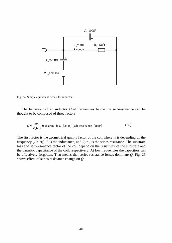
where f is the operating frequency, and Rm(f) and Xm(f) are the real and imaginary part of the inductor impedance (Z), respectively. Fig. 24 shows a simple inductor equivalent circuit. This circuit is used to demonstrate importance of different parasitic on Q. In the figure Ls is the inductance of the device, Rs is the series resistance, Cs is the series parasitic capacitance, Cp is the parasitic capacitance to the substrate, and Rsub is the substrate resistance.
39
Rs=1.6ΩLs=5nH
Cs=100fF
Cp=200fF
Rsub=200kΩ
Fig. 24. Simple equivalent circuit for inductor.
The behaviour of an inductor Q at frequencies below the self-resonance can be thought to be composed of three factors
( ) ( ) ( factorresonanceselffactorlosssubstrate ⋅⋅≈ω
ω
sRLQ ) . (35)
The first factor is the geometrical quality factor of the coil where ω is depending on the frequency (ω=2πf), L is the inductance, and Rs(ω) is the series resistance. The substrate loss and self-resonance factor of the coil depend on the resistivity of the substrate and the parasitic capacitance of the coil, respectively. At low frequencies the capacitors can be effectively forgotten. That means that series resistance losses dominate Q. Fig. 25 shows effect of series resistance change on Q.
40

0
10
20
30
40
50
60
0 2 4 6
Frequency [GHz]
Q
8
R s
0.75R s
0.5R s
Fig. 25. Simulated effect of series resistance change on Q. Series resistance is expected to behave as f .
Optimization of the series resistance for given inductance for a planar inductor on a low-loss substrate leads to linear dependence between the coil area and Q [61, P3]:
skinout2Dmax /81 δDQ ≈− , (36)
where Dout is the outer diameter of the coil, and δskin is the skin depth. Good example that demonstrates how bigger size increases the Q is the LTCC coil presented in [62]. It has reported Q of 65 at 1 GHz and inductance 3.8 nH. Size however is almost 5mm2. At higher frequencies the parasitic capacitances start to have effect on Q. Fig. 26 shows how the series capacitance changes the self-resonance frequency and the Q.
41

0
5
10
15
20
25
30
35
0 2 4 6 8
Frequency [GHz]
Q
C s
0.5C s
2C s
1.5C s
Fig. 26. Simulated effect of the series capacitance on inductor self-resonance frequency and Q. Series resistance is expected to behave as f .
The inductance of the toroidal coil is
coil
2torus
20
2rrNL rµµ
= , (37)
and
torusout
coil 2rDr −= , (38)
where N is the number of turns, µ0 is the vacuum permeability, and µr is the relative magnetic permeability, rtorus is the radius of the torus cross-section, rcoil is the radius of the coil. Different dimensions of the 3D coil are shown in Fig. 27.
42

D
rtorus rcoil
Fig. 27. Top and cross-section view of the toroidal inductor. The series resistance, when the thickness of the wire is much less than the width of the wire, is
)2()(
coilcoilskin
torus2
sNrrNfRs ⋅−⋅
⋅⋅⋅⋅=
πδρπα , (39)
where α(f) is a coefficient taking into account current crowding effects, ρ the resistivity, and scoil the separation between the turns of the coil. The current crowding effect is the tendency of the current in neighbouring conductors to change the current distribution inside the conductor. This increases the series resistance. In addition, the skin effect has a well-known frequency dependency:
f⋅⋅=
πµµρδ
0skin . (40)
43

Dependency of the Q on device geometry can be derived also for the toroidal coil. By combining (35) and (37)-(40), the maximum estimate for a toroidal coil Q at low frequencies can be derived
coil
coilcoiltorus03Dmax )(
)2(rf
sNrrfQ r
⋅⋅−⋅⋅⋅⋅
⋅⋅
=− απ
ρπµµ . (41)
As a result the Q of the toroidal inductor is found to depend on rtorus.
Fig. 28 shows the Q of a toroidal and a planar coil as a function of the outer diameter. The Q of the planar coil was plotted using (36). In the case of a toroidal coil, we attempted to design a 5 nH coil with a ratio of 0.2 between 2rtorus and Dout. Both coils are made of gold. The height of the conductor is 8 µm and the frequency is 1 GHz.
0
20
40
60
80
100
120
140
160
180
200
0 200 400 600 800 1000 1200 1400 1600
Outer diameter [µm]
Q v
alue
Fig. 28. Simulated Q versus outer diameter of optimised planar (dashed line) and toroidal (solid line) inductor at frequency 1 GHz. The inductance is 5 nH for both devices and the gold thickness is 8 µm. There is ratio of 0.2 between 2rtorus and Dout from ref. [P3]. It can be seen that the Q of the toroidal inductor exceeds the Q of the optimised planar coil with similar outer diameter by about a factor two. For example, Q of 175 can be reached for an ideal toroidal inductor with Dout =1.5 mm and rtorus =150 µm. Table V gives a summary of different microfabricated inductors. The measurement results listed
44

in the table are quite far from simulated absolute maximum. One reason is that the process often limits the loop size of the three dimensional coil. For instance in micro-replication process used in [P3] the radius of the torus was limited to 120 µm. Therefore, current design doesn’t use the available area optimally. Other reasons for lower than simulated performance are the current crowding, substrate losses (planar inductors) and contact resistance between two sides (micro-replicated inductor). Chua et al [63] uses electroplating to decrease this contact resistance. In addition, they achieve very large radius of the inductor with their self-assembly method. However, they have measured the inductor Q using low frequency set-up and furthermore taken away the self-resonance term. The self-resonance is in one case at 2.2 GHz and it can ruin otherwise very good performance. Therefore it is difficult to compare their results with the rest of the measurements that are done using high frequency S-parameter technique. Comparison of other results in Table V and 3D micro-replicated inductor presented in this thesis [P3] shows that the three dimensional inductors give significantly higher Q close to 1 GHz than a planar inductor. Microreplicated inductor [P3] has the highest reported Q at 1 GHz for inductors that occupy less than 1mm2 area.
45

TABLE V SUMMARY OF MICROFABRICATED INDUCTORS
Authors Year Inductance [nH]
Q (1GHz)
Peak Q Comments
Ermolov et al [P3] 2004 6 37 50 at 3 GHz microreplicated Zuo et al [64] 2003 10 24 24 at 1 GHz Magnetic assembly, IC
post processing Chua et al [63] 2003 7.5 85 (1) 85 (1) at 1 GHz Self assembly with
stress, IC post processing
Chua et al [63] 2003 4 60 (2) 60 (2) at 1 GHz Self assembly with stress, IC post processing
Huo et al [65] 2002 5.2 20 20 at 1 GHz Planar IC inductor with thick electroplating
Lankadawala et al [66]
2002 4.2 4.5 10.5 at 6 GHz Planar IC inductor with thick electroplating
Piernas et al [67] 2002 4.9 - 35.9 at 4.7 GHz
2D planar inductor
Sutono et al [62] 2001 3.8 65 78 at 1.9 GHz LTCC, size ~5mm2
Chen et al [68] 2001 2.6 10 21 at 4.5 GHz IC post processing Dahlmann et al [69]
2001 2 7 20 at 3 GHz Self assembly by solder re-flow, IC post processing
Lubecke et al [70] 2001 6.7 12 13 at 2 GHz Self assembly with stress, IC post processing
Yoon et al [71] 1999 5 13 50 at 5 GHz 3D solenoid, IC post processing
Yoon et al [72] 1999 14 33 38 at 1.8 GHz 3D solenoid, IC post processing
Kim et al [73] 1999 2.8 20 29 at 2 GHz Bondwires form inductor
Kim and Allen [74]
1998 5.1 13 38 at 5.8GHz 3D solenoid, IC post processing
Young et al [75] 1997 4.8 30 30 at 1 GHz Manual assembly of inductor core
(1) This Q is not comparable with others. The Q is not calculated from S-parameters. It is calculated
by measuring the impedance. Impedance measurement method is utilized usually only at low frequencies well below 1 GHz for inductor Q value calculation. In addition, the effect of the self-resonance is removed from Q. The self-resonance is at 2.2 GHz and should have notable effect on Q at 1 GHz.
(2) This Q is not comparable with others. The Q is not calculated from S-parameters. In addition, the effect of the self-resonance is removed from Q. The self-resonance is at 4.2 GHz and should have notable effect on Q at 1GHz.
46
4.2 Microreplication The idea with polymer replication is to use the accuracy and small features available, for example, in silicon micromachining processes, in combination with the production economy from the optical data storage industry (cf. CD/DVD fabrication technology) [76], [77]. The manufacturing process steps for the toroidal inductor are illustrated in Fig. 29. Typically, a master structure is produced in silicon or glass with the desired geometry. Electroforming a negative copy of the master then creates a mould insert. Finally, polymer replicas can be produced in large quantities by using these inserts in different replication methods such as injection moulding, casting, or hot embossing [78]. 4.2.1 Substrate material Depending on the physical and chemical requirements of the final product, there is a wide range of thermoplastic and thermosetting polymer materials to choose from. Injection moulded thermoplastics are well suited as substrate material for RF inductor. The reason for this is twofold. First, the dielectric properties for some of the thermoplastic polymers are superior compared to thermosetting materials. This is specifically the case for the cyclo-olefin polymer (COP). Second, it is easier to obtain flat and stress-free wafers by injection moulding of thermoplastic polymers compared to casting with thermosetting polymers. Also, if one adds the aspect of production economy, injection moulding is to be favored.
4.2.2 Master fabrication Master structure contains same 3D surface form that is transferred into the injection moulded substrate. The masters can be produced for instance by isotropic silicon etching [79]. This is shown in Fig. 29(a) and (b). In order to achieve high isotropy, it is necessary to etch without stirring and with the wafer lying horizontally and the etch features upwards. A solution consisting of 96 : 4 or 91 : 9 HNO (69%) :HF (50%) is proven to work [P3]. Thus, no acetic acid is used. This gives a polishing etch with smooth surfaces. The etch rate is approximately 1µm/min at room temperature. The isotropy, or width/depth ratio, that can be attained is good approximately 1:0.96.
4.2.3 Replication step and substrate moulding
Replication step creates a 3D mirror image of the surface of the silicon master structure. This is shown in Fig. 29(c). In this step, the silicon master structure is transferred into a 300µm thick metallic counterpart by electroforming. This is achieved by plating with nickel from a sulfamate electrolyte. The substrate for the toroidal inductor is then made by injection moulding. This is shown in Fig. 29(d). Several different polymers can be used as substrate material, for instance, polycarbonate (PC) and COP.
47

Fig. 29. Manufacturing process steps for the microreplicated toroidal RF inductor from ref. [P3].
48

4.2.4 Conductor lines
Conductor lines can be patterned by various methods depending on the required accuracy. One way is to define the conductors lithographically. Prior to patterning, the substrates are sputtered with a 50-nm-thick gold seed layer. Then a conformal photoresist layer is applied on the polymer substrates. After the resist development, electronic-quality pure gold is deposited by electroplating into the sidewall resist structures. Fig. 29(e) and (f) depict an example of the process. After the electroplating, the seed layer is etched away in order to isolate the structures.
4.2.5 Assembly of inductor
In order to obtain a complete toroidal RF inductor, two metallized substrates have to be bonded. This is achieved by thermo compression (at 75-bar pressure) with a heat-curing adhesive. The aim is to achieve a low contact resistance by ensuring a proper metal–metal contact at the gold interfaces. The inductor will exhibit a serial resistance containing contributions from both contact points, as well as intrinsic material properties of the electroplated gold. The contact resistance is also affected by alignment errors.
49

50

5. Conclusions Main results of this thesis are: I. Novel concepts of RF MEM components This thesis presents three different MEM capacitors. First, a novel two-state capacitor that has a temperature compensation structure based on geometrical effects is demonstrated. Secondly, a novel three-state capacitor structure is demonstrated. The advantage of this structure is that one additional stable state is added into the two-state capacitor without any increase in the device area. The process required for the three-state capacitor is the same that is used to create a continuously tunable capacitor. Thirdly, a continuously tunable capacitor that has a nominal capacitance of 1.58 pF and achieves a tuning range of 2.25:1 with parasitics is demonstrated. A novel high-Q three-dimensional micro-replicated inductor is presented in this thesis. An inductor has usually the lowest Q for instance in a matching network. Thus it is a very critical component. It can be shown that in theory the Q if an optimized inductor is linearly dependent on the inductor area. Both 2D and 3D coils follow this dependence. However, for the same substrate area a 3D-coil has a higher theoretical limit in terms of the Q than a 2D-inductor. Therefore, 3D-coils appear to be superior in RF applications. Toroidal coils have also an additional advantage that most electro-magnetic field is restricted inside the torus. However, it is difficult to create large 3D-coils using an IC processes. Solution presented in this thesis is a novel high-Q three-dimensional micro-replicated inductor. Electrical measurements show that the inductor with an inductance of 6.0 nH exhibits a peak quality factor of 50 at a frequency of 3 GHz. A model verified by the measurement results shows that further improvement is still possible. Fig. 30 shows picture gallery of the components. II. Improved reliability of MEM capacitor A novel two-state capacitor that has a temperature compensation structure based on geometrical effects is demonstrated. Measurements show that the fluctuation of COFF is less than 6%, CON is less than 2 %, and Upull-in is less than 5% over a 100°C temperature range. Temperature compensation principle is not limited to MEM capacitors. The compensation principle can be applied to many other MEM devices like MEM accelerometers. Charging of dielectric layer is also now better understood than a couple of years ago. Temperature dependent stress and charging of dielectric layer add complexity to MEM capacitor design. However, it is seen that with proper designing their effect can be reduced to an acceptable level. III. Design rules for MEM capacitor Summary of the MEM capacitor design rules and the design flow is depicted in Fig. 31.
51

(a) (b)
(c) (d)
(e)
52

Previous page Fig. 30. (a) Photograph of a two-state MEM capacitor from ref. [P2], (b) Photograph of a three-state MEM capacitor with springs that connect the suspended membrane to the anchoring from ref. [P2], (c) Photograph of a two-gap MEM tunable capacitor from ref. [P2], (d) Photograph of temperature compensated MEM capacitor from ref. [P4], and (e) Photograph of microreplicated toroidal inductor from ref. [P3].
•COFF
•CON
αα
α)1(2
231 2
3
−⎟⎠⎞
⎜⎝⎛=
−inpull
release
UU
Switching speed τ
•Upull-in
•URelease
•UHold-down
• tdielectric
⇒ tgap
•Electrical reliability testing•Emax
1.
2.
Maximum RF signal
Thermal stability frame
roughnessrhold
on
tEUA
C
ε
ε
+=⎥⎦
⎤⎢⎣
⎡
max
max
4.
5.
maxEtU dielectrichold =
Spring constant k
mk
=0ω
3.
2RF
RFuF ∝
Separate / common control & signal electrode
•Gas pressure•Sacrificial holes
Q Substrate losses
Rp(leakage current)
Rs(Metal thickness)
Control circuit
DC blocking capacitors
Power consumptionPower consumption
Fig. 31. Summary of the MEM capacitor design rules and design flow.
53

54

References [1] H. Nieminen, T. Ryhänen, V. Ermolov, and S. Silanto, ”Method and structure
that forms firm boundary conditions for metal suspended structures”, U. S. Patent 6 557 413, May 6, 2003.
[2] V. Ermolov, H. Nieminen, K. Nybergh, T. Ryhänen, and S. Silanto, “Microsystem Technologies for Mobile Communication Products”, Surface Mount Technology International, 2001, pp. 710-717.
[3] H. Nieminen, J. Kankaanpää, V. Ermolov, S. Silanto, and T. Ryhänen, ”RF MEMS for 0.8GHz-2.5GHz applications”, to be published in 5th workshop on MEMS for millimeter wave communications MEMSWAVE 2004, 2004.
[4] T. Veijola, T. Tinttunen, H. Nieminen, V. Ermolov, and T. Ryhänen, “Gas Damping Model for a RF MEMS Switch and Its Dynamic Characteristics”, IEEE MTT-S International Microwave Symposium Digest, Vol. 2, 2002, pp. 1213-1216.
[5] T. Tinttunen, T. Veijola, H. Nieminen, V. Ermolov and T. Ryhänen, "Static Equivalent Circuit Model for a Capacitive MEMS RF Switch", Modeling and Simulation of Microsystems, NANOTECH 2002, 2002, pp. 166-169.
[6] K. Petersen, “Micromechanical membrane switches on silicon”, IBM Journal of Research and Development, pp. 376-385, Vol. 23, 1979.
[7] S. Majumder, J. Lampen, R. Morrison, and J. Maciel, “A packaged, high-lifetime ohmic MEMS RF switch”, IEEE MTT-S International Microwave Symposium Digest, Vol. 3, 2003, pp. 1935-1938.
[8] V. Kaajakari, T. Mattila, A. Oja, J. Kiihamäki, and H. Seppä, “Square-extensional mode single-crystal silicon micromechanical resonator for low-phase-noise oscillator applications”, IEEE Electron Device Letters, pp. 173-175, Vol. 25, 2004.
[9] A. Alastalo, T. Mattila, and H. Seppä, “Analysis of a MEMS transmission line”, IEEE Transactions on Microwave Theory and Techniques, pp. 1977-1981, Vol. 51, 2003.
[10] R. Borwick, P. Stupar, J. DeNatale, R. Anderson, and R. Erlandson, “Variable MEMS capacitors implemented into RF filter systems”, IEEE Transactions on Microwave Theory and Techniques, pp. 315-319, Vol. 51, 2003.
[11] A. Fukuda, H. Okazaki, T. Hirota, and Y. Yamao, “Novel 900 MHz/1.9 GHz dual-mode power amplifier employing MEMS switches for optimum matching”, IEEE Microwave and Wireless Components Letters, Vol. 14, pp. 121-123, 2004.
55

[12] J. Papapolymerou, K. Lange, C. Goldsmith, A. Malczewski, and J. Kleber, “Reconfigurable double-stub tuners using MEMS switches for intelligent RF front-ends”, IEEE Transactions on Microwave Theory and Techniques, pp.271-278, Vol. 51, 2003.
[13] H. Kim, S. Jung, K. Kang, J.-H. Park, and Y.-K. Kim, ”Low-loss analog and digital micromachined impedance tuners at the Ka-band”, IEEE Transactions on Microwave Theory and Techniques, pp.2394–2400, Vol. 49, 2001.
[14] H. Kim, J. Park, Y. Kim, and Y. Kwon, “Millimeterwave micromachined tunable filters”, IEEE MTT-S International Microwave Symposium Digest, 1999, pp. 1235-1238.
[15] R. Streeter, C. Hall, R. Wood, and R. Madadevan, “VHF high-power tunable RF bandpass filter using microelectromechanical (MEM) microrelays”, International Journal of RF and Microwave Computer-Aided Engineering, pp. 261-275, Vol. 11, 2001.
[16] R. Simons, D. Chun, and L. Katehi, “Micromechanical system actuators for antenna reconfigurability”, IEEE MTT-S International Microwave Symposium Digest, 2001, pp. 215-218.
[17] J.-C. Chiao, Y. Fu, I. Chio, M. Delisio, and L. Lin, “MEMS reconfigurable Vee antenna”, IEEE MTT-S International Microwave Symposium Digest, 1999, pp. 1515-1518.
[18] G.-L. Tan, R. Mihailovich, J. Hacker, J. DeNatale, and G. Rebeiz, “Low-loss 2- and 4-bit TTD MEMS phase shifters based on SP4T switches”, IEEE Transactions on Microwave Theory and Techniques, pp.297-304, Vol. 51, 2003.
[19] A. Malczewski, S. Eshelman, B. Pillans, J. Ehmke, and C. Goldsmith, “X-band RF MEMS phase shifters for phased array applications”, IEEE Microwave and Guided Wave Letters, pp.517-519, Vol. 9, 1999.
[20] M. Kim, R. Mihailovich, and J. DeNatale, “A DC-to-40GHz four-bit RF MEMS true-time delay network”, IEEE Microwave and Wireless Components Letters, pp.56–58, Vol. 11, 2001.
[21] C. Goldsmith, J. Ehmke, A. Malczewski, B. Pillans, S. Eshelman, Z. Yao, J. Brank, and M. Eberly, “Lifetime characterization of capacitive RF MEMS switches”, IEEE MTT-S International Microwave Symposium Digest, Vol. 1, 2001, pp. 227-230.
[22] L. Dussopt and G. Rebeiz, “Intermodulation distortion and power handling in RF MEMS switches, varactors, and tunable filters”, IEEE Transactions on Microwave Theory and Techniques, Vol. 51, pp. 1247-1256, 2003.
56

[23] M. Kim, J. Hacker, R. Mihailovich, and J. DeNatale, “A monolithic MEMS switched dual-path power amplifier”, IEEE Microwave and Wireless Components Letters, pp. 285-286, Vol. 11, 2001.
[24] O. Larsson, "Polymeric Microstructures and Replication Techniques", Proceedings of the Micro Structure Workshop, Uppsala, March 26-27, 1996, p. 1.
[25] O. Larsson, O. Öhman, A. Billman, L. Lundbladh, C. Lindell, and G. Palmskog, "Silicon Based Replication Technology of 3-D-Microstructures by Conventional CD-Injection Molding Techniques," International Conference on Solid-state Sensors, Actuators and Microsystems, Transducers '97, pp. 1415-1418, 1997.
[26] H. Elderstig and O. Larsson, "Polymeric MST - High precision at low cost", Journal of Micromechanics and Microengineering, pp. 89.92, Vol. 7, 1997.
[27] W. Weaver, S. Timoshenko, and D. Young, Vibration problems in engineering, 5th edition, John Wiley & Sons, New York, 1990.
[28] J. Berqvist, F. Rudolf, J. Maisana, F. Parodi, and M. Rossi, “A silicon condencer microphone with a highly perforated backplane”, IEEE Solid-state Sensors and Actuator Workshop Diggest, 1991, pp. 266-269.
[29] S. Dushman and J. Lafferty, Scientific foundations of vacuum technique, John Wiley & Sons, New York, 1962.
[30] G. Rebeiz, RF MEMS Theory, Design, and Technology, New Jersey: Wiley, 2003, pp. 21-57.
[31] L. Dussopt and G. Rebeiz, “High-Q millimeter-wave MEMS varactor: Extended tuning range and discrete-position designs”, IEEE MTT-S International Microwave Symposium Digest, 2002, pp. 1205-1208.
[32] T. Rijks, J. van Beek, P. Steeneken, M. Ulenaers, J. De Coster, and R. Puers, “RF MEMS tunable capacitors with large tuning ratio”, IEEE International Conference on Micro Electro Mechanical Systems, 2004, pp. 777-780.
[33] J. De Coster, R. Puers, H. Tilmans, J. van Beek, and T. Rijks, “Variable RF MEMS capacitors with extended tuning range”, International Conference on Solid-state Sensors, Actuators and Microsystems, TRANSDUCERS ‘03, pp. 1784-1787, 2003.
[34] C. Tsai, P. Stupar, R. Borwick, M. Pai, and J. DeNatale, “An isolated tunable capacitor with a linear capacitance voltage behavior”, Solid-State Sensors, Actuators and Microsystems, International Conference on Solid-state Sensors, Actuators and Microsystems, TRANSDUCERS’03, Vol. 1, 2003, pp. 833-836.
57

[35] O. Altug and G. Fedder, “CMOS-compatible RF-MEMS tunable capacitors”, IEEE MTT-S International Microwave Symposium Digest, Vol. 1, 2003, pp. A97-A100.
[36] A. Gallant and D. Wood, “Nickel electroplated widely tunable micromachined capacitor”, IEE Electronics Letters, Vol. 38, pp.1392-1393, 2002.
[37] G. Ionis, A. Dec, and K. Suyama, “Differential multi-finger MEMS tunable capacitors for RF integrated circuits”, IEEE MTT-S International Microwave Symposium Digest, Vol. 1, 2001, pp. 345-348.
[38] R. Borwick, P. Stupar, J. DeNatale, R. Anderson, C. Tsai, and K. Garrett, “Variable MEMS capacitors implemented into RF filter systems”, IEEE International Conference on Micro Electro Mechanical Systems, 2002, pp. 669-672.
[39] G. Ionis, A. Dec, and K. Suyama, “A zipper-action differential micro-mechanical tunable capacitor”, IEEE International Conference on Micro Electro Mechanical Systems, 2001, pp. 29-32.
[40] J. Park, Y. Yee, H. Nam, and J. Bu, “Micromachined RF MEMS tunable capacitors using piezoelectric actuators”, IEEE MTT-S International Microwave Symposium Digest, Vol. 3, 2001, pp. 2111-2114.
[41] J. Zou, C. Liu, J. Schutt-Aine, J. Chen and S. Kang, “Development of a wide tuning range MEMS tunable capacitor for wireless communication systems”, IEDM Technical Digest, 2000, pp. 403-406.
[42] J-B. Yoon and C. Nguyen, “A high-Q tunable micromechanical capacitor with movable dielectric for RF applications”, IEDM Technical Digest, 2000, pp. 489-492.
[43] J. Yao, S. Park, and J. DeNatale, “High tuning-ratio MEMS based tunable capacitors for RF communication applications”, IEEE Solid-state Sensors and Actuators Workshop Digest, 1998, pp. 124-127.
[44] Z. Feng, W. Zhang, B. Su, K. Harsh, K. Gupta, V. Bright, and Y. Lee, “Design and modeling of RF MEMS tunable capacitors using electro-thermal actuators”, IEEE MTT-S International Microwave Symposium Digest, Vol. 4, 1999, pp. 1507-1510.
[45] A. Dec and K. Suyama, “Micromachined Electro-Mechanically Tunable Capacitors and Their Applications to RF IC’s”, IEEE Transactions on Microwave Theory and Techniques, Vol. 46, pp. 2587-2596, 1998.
[46] D. Young and B. Boser, “A micromachined variable capacitor for monolithic low-noise VCOs”, IEEE Solid-state Sensors and Actuator Workshop Diggest, 1996, pp. 86-89.
58

[47] R. Guardia, A. Dehe, R. Aigner and L. Castañer, “New Current Drive Method to Extend the Stable Operation Range of Electrostatic Actuators: Experimental Verification”, International Conference on Solid-state Sensors, Actuators and Microsystems, TRANSDUCERS '01, Vol. 1, 2001, pp. 760-763.
[48] L. Castañer and S. Senturia, “Speed-energy optimization of electrostatic actuators based on pull-in”, IEEE Journal of Microelectromechanical Systems, Vol. 8, pp. 290-298, 1999.
[49] J. Kyynäräinen, A. Oja and H. Seppä, “Increasing the Dynamic Range of Micromechanical Moving-Plate Capacitor”, Analog Integrated Circuits and Signal Processing, Vol. 29, pp. 61-70, 2001.
[50] J. Zou, C. Liu, J. Schutt-Aine, J. Chen and S. Kang, “Development of a wide tuning range MEMS tunable capacitor for wireless communication systems”, IEDM Technical Digest, 2000, pp. 403-406.
[51] J. Seeger and S. Crary, “Stabilization of Electrostatically Actuated Mechanical Devices”, International Conference on Solid-state Sensors, Actuators and Microsystems, TRANSDUCERS '97, Vol. 2, 1997, pp. 1133-1136.
[52] E. Fourn, A. Pothier, C. Champeaux, P.Tristant, A. Catherinot, P. Blondy, G. Tanne, E. Rius, C. Person, and F. Huret, “MEMS switchable interdigital coplanar filter ”, IEEE Transactions on Microwave Theory and Techniques, Vol. 51, pp. 320-324, 2003.
[53] X. Lafontan, P. Schmitt, F. Pressecq, Q. Duong, D Veyrie, P. Pons, J. Kuchenbecker, L. Rabbia, F. Flourens, K. Grenier, and R. Plana, ”Sensitivity of RF MEMS to environmental stresses”, 4th workshop on MEMS for millimeter wave communications MEMSWAVE 2003, 2003, pp. A-15-18.
[54] X.Chauffleur, L. Rabbia, F. Flourens, P. Pons, and R. Plana, ”Thermomechanical simulation of RF MEMS process”, 4th workshop on MEMS for millimeter wave communications MEMSWAVE 2003, 2003, pp. B-25-28.
[55] G. Blaise, “Charge trapping in thin SiO2 layers: Application to the breakdown of MOS”, IEEE 1996 Annual Report: Conference on Electrical Insulation and Dielectric Phenomena, pp. 24-27, 1996.
[56] O. Bochobza-Degani, E. Socher, and Y. Nemirovsky, “On the effect of residual charges on the pull-in parameters of electrostatic actuators”, Sensors and Actuators A, Vol. 97-98, pp. 563-568, 2002.
[57] F. W. Grover, Inductance Calculations. New York: Dover, 1973.
[58] C. Yue and S. Wong, “On-chip spiral inductors with patterned ground shields for Si-based RF IC’s,” IEEE J. Solid-State Circuits, pp. 743-752, May 1998.
59
[59] A. Niknejad and R. Meyer, “Analysis, design and optimization of spiral inductors and transformers for Si RF IC’s,” IEEE J. Solid-State Circuits, vol.33, pp. 1470-1481, October 1998.
[60] H. Lakdawala, X. Zhu, H. Luo, S. Santhanam, L. Carley, and G. Fedder, ”Micromachined high Q inductors in a 0.18-um copper interconnect low-K dielectric CMOS process,” IEEE J. Solid-State Circuits, vol. 37, March 2002.
[61] T. Varpula, “Optimising planar inductors”, VTT Automation, Helsinki, Finland, Research Notes 2017, ISBN 951-38-5641-0, 2000.
[62] A. Sutono, D. Heo, Y-J. Chen, and J. Laskar, “High-Q LTCC-based passive library for wireless system-on-package (SOP) module development”, IEEE Transactions on Microwave Theory and Techniques, Vol. 49, pp. 1715-1724, 2001.
[63] C. Chua, D. Fork, K. Van Schuylenbergh, and J-P. Lu, “Out-of-plane high-Q inductors on low-resistance silicon”, IEEE Journal of Microelectromechanical Systems, Vol. 12, pp. 989-995, 2003.
[64] J. Zou, L. C. Liu, D. Trainor, J. Chen, J. Schutt-Aine, and P. Chapman, “Development of three-dimensional inductors using plastic deformation magnetic assembly (PDMA)”, IEEE Transactions on Microwave Theory and Techniques, Vol. 51, pp. 1067-1075, 2003.
[65] X. Huo, K. Chen, and P. Chan, “Silicon-based high-Q inductors incorporating electroplated copper and low-K BCB dielectric”, IEEE Electron Device Letters, Vol. 23, pp. 520-522, 2002.
[66] H. Lakdawala, X. Zhu, H. Luo, S. Santhanam, L. Carley, and G. Fedder, “Micromachined high-Q inductors in a 0.18-µm copper interconnect low-k dielectric CMOS process”, IEEE Journal of Solid-State Circuits, Vol. 37, pp. 394-403, 2002.
[67] B. Piernas, K. Nishikawa, K. Kamogawa, T. Nakagawa, and K. Araki, “High-Q factor three-dimensional inductors”, IEEE Transactions on Microwave Theory and Techniques, Vol. 50, pp. 1942-1949, 2002.
[68] Y. Chen, Y. Yoon; J. Laskar, and M. Allen, “A 2.4 GHz integrated CMOS power amplifier with micromachined inductors”, IEEE MTT-S International Microwave Symposium Digest, Vol. 1, 2001, pp. 523-526.
[69] G. Dahlmann, E. Yeatman, P. Young, I. Robertson, and S. Lucyszyn, “MEMS high Q microwave inductors using solder surface tension self-assembly”, IEEE MTT-S International Microwave Symposium Digest, Vol. 1, 2001, pp. 329-332.
60

[70] V. Lubecke, B. Barber, E. Chan, D. Lopez, M. Gross, and P. Gammel, “Self-assembling MEMS variable and fixed RF inductors”, IEEE Transactions on Microwave Theory and Techniques, Vol. 49, pp. 2093-2098, 2001.
[71] J-B. Yoon, C-H. Han, E. Yoon, and C-K. Kim, “Monolithic integration of 3-D electroplated microstructures with unlimited number of levels using planarization with a sacrificial metallic mold (PSMM)”, IEEE International Conference on Micro Electro Mechanical Systems, 1999, pp. 624-629.
[72] J-B. Yoon, C-H. Han, E. Yoon, and C-K. Kim, “High-performance three-dimensional on-chip inductors fabricated by novel micromachining technology for RF MMIC”, IEEE MTT-S International Microwave Symposium Digest, Vol. 4, 1999, pp. 1523-1526.
[73] S-J. Kim, Y-G. Lee, S-K. Yun, and H-Y. Lee, “Realization of high-Q inductors using wirebonding technology”, IEEE Asia Pacific Conference on ASICs, 1999, pp. 13-16.
[74] Y-J. Kim and M. Allen, “Suface micromachined solenoid inductors for high frequency applications”, IEEE Transactions on Components, Packaging, and Manufacturing Technology, Vol. 21, pp. 26-33, 1998.
[75] D. Young, V. Malba, J-J. Ou, A. Bernhardt, and B. Boser, “Monolithic high-performance three-dimensional coil inductors for wireless communication applications”, IEDM Technical Digest, 1997, pp.67-70.
[76] O. Öhman, H. Sjödin, B. Ekström, and G. Jacobsson, “Microfluidic structure and process for its manufacture,” Pharmacia Biosensor, Uppsala, Sweden, Int. Publication WO 91/16 966, Dec. 27, 1994.
[77] B. Ekström, G. Jacobson, O. Öhman, and H. Sjödin, “Microfluidic structure and process for its manufacture,” U.S. Patent 5 376 252, Dec. 27, 1994.
[78] O. Rötting, W. Röpke, H. Becker, and C. Gärtner, “Polymer microfabrication technologies,” Microsyst. Technol., vol. 8, pp. 32–36, 2002.
[79] G. Meaden, Electrical resistance of metals, Plenum Press, New York, p. 1, 1965.
61

62

Paper reprints The article [P1], published in Electronics Letters, is reprinted with permission from The Institution of Electrical Engineering. The article [P2], published in Journal of Micromechanics and Microengineering, is reprinted with permission from IOP Publishing Ltd. The article [P3], published in IEEE Transactions on Microwave Theory and Techniques, is reprinted with permission from The Institution of Electrical and Electronics Engineers, Inc. The article [P4], published in IEEE Microelectromechanical Systems, is reprinted with permission from The Institution of Electrical and Electronics Engineers, Inc. The article [P5], published in Sensors and Actuators A, is reprinted with permission from Elsevier.
63


![Automated Design Strategy for High Performance Mixed ...€¦ · IL-PLL DMDLL DPLL MDLL IL-PLL Freq. [GHz] 1.2 (0.5-1.6) 1.5 (0.8-1.8) 1.5 (0.8-1.8) 1.6 0.216 Ref. [MHz] 300 (40-300)](https://img.pdfslide.us/doc/110x75/60d300bb6a843e51fd2d6423/automated-design-strategy-for-high-performance-mixed-il-pll-dmdll-dpll-mdll.jpg)


![THz Communications An Option for Wireless Networks …¼rner.pdf0.2 0.4 0.6 0.8 1 eit Oberflächenhöhe [mm] Raufaser 100 150 200 250 300 350 400 450 0 0.2 0.4 0.6 0.8 1 f [GHz] or](https://img.pdfslide.us/doc/110x75/5ee176cbad6a402d666c5672/thz-communications-an-option-for-wireless-networks-rnerpdf-02-04-06-08-1-eit.jpg)


![A 130 GHz Electro-Optic Ring Modulator with Double-Layer ......the ring resonator modulators with graphene on top of them [21 23]. These kinds of electro-optic modulators have both](https://img.pdfslide.us/doc/110x75/60a6d2dc89cc8055dc7fd0f9/a-130-ghz-electro-optic-ring-modulator-with-double-layer-the-ring-resonator.jpg)