Embed Size (px)
Citation preview
MD7IC2755NR1 MD7IC2755GNR1
1RF Device DataFreescale Semiconductor
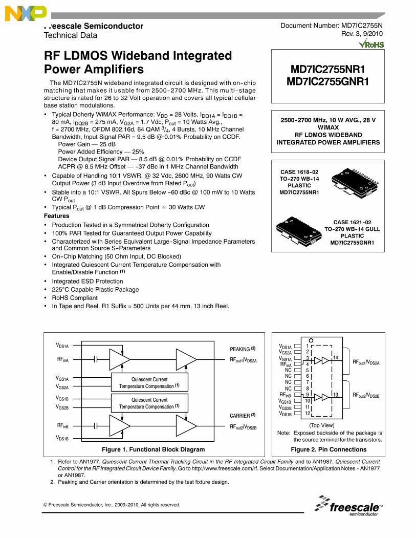
RF LDMOS Wideband IntegratedPower AmplifiersThe MD7IC2755N wideband integrated circuit is designed with on--chip
matching that makes it usable from 2500--2700 MHz. This multi --stagestructure is rated for 26 to 32 Volt operation and covers all typical cellularbase station modulations.
• Typical Doherty WiMAX Performance: VDD = 28 Volts, IDQ1A = IDQ1B =80 mA, IDQ2B = 275 mA, VG2A = 1.7 Vdc, Pout = 10 Watts Avg.,f = 2700 MHz, OFDM 802.16d, 64 QAM 3/4, 4 Bursts, 10 MHz ChannelBandwidth, Input Signal PAR = 9.5 dB @ 0.01% Probability on CCDF.Power Gain 25 dBPower Added Efficiency 25%Device Output Signal PAR 8.5 dB @ 0.01% Probability on CCDFACPR @ 8.5 MHz Offset --37 dBc in 1 MHz Channel Bandwidth
• Capable of Handling 10:1 VSWR, @ 32 Vdc, 2600 MHz, 90 Watts CWOutput Power (3 dB Input Overdrive from Rated Pout)
• Stable into a 10:1 VSWR. All Spurs Below --60 dBc @ 100 mW to 10 WattsCW Pout
• Typical Pout @ 1 dB Compression Point ≃ 30 Watts CWFeatures• Production Tested in a Symmetrical Doherty Configuration• 100% PAR Tested for Guaranteed Output Power Capability• Characterized with Series Equivalent Large--Signal Impedance Parameters
and Common Source S--Parameters• On--Chip Matching (50 Ohm Input, DC Blocked)• Integrated Quiescent Current Temperature Compensation with
Enable/Disable Function (1)
• Integrated ESD Protection• 225°C Capable Plastic Package• RoHS Compliant• In Tape and Reel. R1 Suffix = 500 Units per 44 mm, 13 inch Reel.
Figure 1. Functional Block Diagram Figure 2. Pin Connections
1. Refer to AN1977, Quiescent Current Thermal Tracking Circuit in the RF Integrated Circuit Family and to AN1987, Quiescent CurrentControl for theRF IntegratedCircuit Device Family. Go to http://www.freescale.com/rf. Select Documentation/ApplicationNotes -- AN1977or AN1987.
2. Peaking and Carrier orientation is determined by the test fixture design.
Note: Exposed backside of the package isthe source terminal for the transistors.
Quiescent CurrentTemperature Compensation (1)
VDS1A
RFinA
VGS1A
RFout1/VDS2A
VGS2A
Quiescent CurrentTemperature Compensation (1)
VDS1B
RFinB
VGS1B
RFout2/VDS2B
VGS2B
VDS1A
RFinA
NC
RFinB
RFout1/VDS2A
1234
78
14
VGS1B91011
VGS2AVGS1A
NC
NC
VGS2B
NC
VDS1B
RFout2/VDS2B13
6
12
(Top View)
5
PEAKING (2)
CARRIER (2)
2500--2700 MHz, 10 W AVG., 28 VWiMAX
RF LDMOS WIDEBANDINTEGRATED POWER AMPLIFIERS
MD7IC2755NR1MD7IC2755GNR1
CASE 1618--02TO--270 WB--14
PLASTICMD7IC2755NR1
CASE 1621--02TO--270 WB--14 GULL
PLASTICMD7IC2755GNR1
Document Number: MD7IC2755NRev. 3, 9/2010
Freescale SemiconductorTechnical Data
© Freescale Semiconductor, Inc., 2009--2010. All rights reserved.
2RF Device Data
Freescale Semiconductor
MD7IC2755NR1 MD7IC2755GNR1
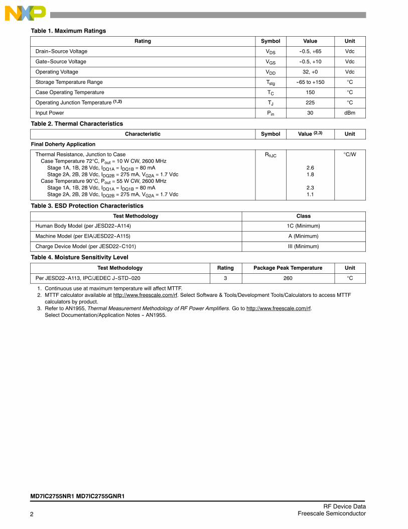
Table 1. Maximum Ratings
Rating Symbol Value Unit
Drain--Source Voltage VDS --0.5, +65 Vdc
Gate--Source Voltage VGS --0.5, +10 Vdc
Operating Voltage VDD 32, +0 Vdc
Storage Temperature Range Tstg --65 to +150 °C
Case Operating Temperature TC 150 °C
Operating Junction Temperature (1,2) TJ 225 °C
Input Power Pin 30 dBm
Table 2. Thermal Characteristics
Characteristic Symbol Value (2,3) Unit
Final Doherty Application
Thermal Resistance, Junction to CaseCase Temperature 72°C, Pout = 10 W CW, 2600 MHz
Stage 1A, 1B, 28 Vdc, IDQ1A = IDQ1B = 80 mAStage 2A, 2B, 28 Vdc, IDQ2B = 275 mA, VG2A = 1.7 Vdc
Case Temperature 90°C, Pout = 55 W CW, 2600 MHzStage 1A, 1B, 28 Vdc, IDQ1A = IDQ1B = 80 mAStage 2A, 2B, 28 Vdc, IDQ2B = 275 mA, VG2A = 1.7 Vdc
RθJC
2.61.8
2.31.1
°C/W
Table 3. ESD Protection Characteristics
Test Methodology Class
Human Body Model (per JESD22--A114) 1C (Minimum)
Machine Model (per EIA/JESD22--A115) A (Minimum)
Charge Device Model (per JESD22--C101) III (Minimum)
Table 4. Moisture Sensitivity Level
Test Methodology Rating Package Peak Temperature Unit
Per JESD22--A113, IPC/JEDEC J--STD--020 3 260 °C
1. Continuous use at maximum temperature will affect MTTF.2. MTTF calculator available at http://www.freescale.com/rf. Select Software & Tools/Development Tools/Calculators to access MTTF
calculators by product.3. Refer to AN1955, Thermal Measurement Methodology of RF Power Amplifiers. Go to http://www.freescale.com/rf.
Select Documentation/Application Notes -- AN1955.
MD7IC2755NR1 MD7IC2755GNR1
3RF Device DataFreescale Semiconductor
Table 5. Electrical Characteristics (TA = 25°C unless otherwise noted)
Characteristic Symbol Min Typ Max Unit
Stage 1 Off Characteristics (1)
Zero Gate Voltage Drain Leakage Current(VDS = 65 Vdc, VGS = 0 Vdc)
IDSS 10 μAdc
Zero Gate Voltage Drain Leakage Current(VDS = 28 Vdc, VGS = 0 Vdc)
IDSS 1 μAdc
Gate--Source Leakage Current(VGS = 1.5 Vdc, VDS = 0 Vdc)
IGSS 1 μAdc
Stage 1 On Characteristics
Gate Threshold Voltage (1)
(VDS = 10 Vdc, ID = 46 μAdc)VGS(th) 1.2 1.9 2.7 Vdc
Gate Quiescent Voltage (1)
(VDS = 28 Vdc, IDQ1A = IDQ1B = 80 mAdc)VGS(Q) 2.7 Vdc
Fixture Gate Quiescent Voltage (2)
(VDD = 28 Vdc, IDQ1A = IDQ1B = 80 mAdc, Measured in Functional Test)VGG(Q) 12 15 18 Vdc
Stage 2 Off Characteristics (1)
Zero Gate Voltage Drain Leakage Current(VDS = 65 Vdc, VGS = 0 Vdc)
IDSS 10 μAdc
Zero Gate Voltage Drain Leakage Current(VDS = 28 Vdc, VGS = 0 Vdc)
IDSS 1 μAdc
Gate--Source Leakage Current(VGS = 1.5 Vdc, VDS = 0 Vdc)
IGSS 1 μAdc
Stage 2 On Characteristics
Gate Threshold Voltage (1)
(VDS = 10 Vdc, ID = 185 μAdc)VGS(th) 1.2 1.9 2.7 Vdc
Gate Quiescent Voltage (1)
(VDS = 28 Vdc, IDQ2B = 275 mAdc)VGS(Q) 2.7 Vdc
Fixture Gate Quiescent Voltage (2)
(VDD = 28 Vdc, IDQ2B = 275 mAdc, Measured in Functional Test)VGG(Q) 12 15 18 Vdc
Drain--Source On--Voltage (1)
(VGS = 10 Vdc, ID = 1 A)VDS(on) 0.2 0.47 1.2 Vdc
Stage 2 -- Dynamic Characteristics (2,3)
Output Capacitance(VDS = 28 Vdc ± 30 mV(rms)ac @ 1 MHz, Vin = 0 Vdc)
Coss 111 pF
Functional Tests (4,5) (In Freescale Doherty Test Fixture, 50 ohm system) VDD = 28 Vdc, IDQ1A = IDQ1B = 80 mA, IDQ2B = 275 mA,VG2A = 1.7 Vdc, Pout = 10 W Avg., f = 2700 MHz, WiMAX, OFDM 802.16d, 64 QAM 3/4, 4 Bursts, 10 MHz Channel Bandwidth, Input SignalPAR = 9.5 dB @ 0.01% Probability on CCDF. ACPR measured in 1 MHz Channel Bandwidth @ ±8.5 MHz Offset.
Power Gain Gps 23 25 31 dB
Power Added Efficiency PAE 23 25 %
Output Peak--to--Average Ratio @ 0.01% Probability on CCDF PAR 8 8.5 dB
Adjacent Channel Power Ratio ACPR --37 --35 dBc
1. Side A and Side B are tied together for this measurement.2. Each side of device measured separately.3. Part internally matched both on input and output.4. Measurement made with device in a Symmetrical Doherty configuration.5. Measurement made with device in straight lead configuration before any lead forming operation is applied.
(continued)
4RF Device Data
Freescale Semiconductor
MD7IC2755NR1 MD7IC2755GNR1
Table 5. Electrical Characteristics (TA = 25°C unless otherwise noted) (continued)
Characteristic Symbol Min Typ Max Unit
Typical Performances (In Freescale Doherty Test Fixture, 50 ohm system) VDD = 28 Vdc, IDQ1A = IDQ1B = 80 mA, IDQ2B = 275 mA,VG2A = 1.7 Vdc, 2500--2700 MHz Bandwidth
Pout @ 1 dB Compression Point, CW P1dB 30 W
IMD Symmetry @ 12 W PEP, Pout where IMD Third OrderIntermodulation 30 dBc(Delta IMD Third Order Intermodulation between Upper and LowerSidebands > 2 dB)
IMDsym 70
MHz
VBW Resonance Point(IMD Third Order Intermodulation Inflection Point)
VBWres 85 MHz
Gain Flatness in 200 MHz Bandwidth @ Pout = 10 W Avg. GF 1.6 dB
Average Deviation from Linear Phase in 200 MHz Bandwidth@ Pout = 30 W CW
Φ 2 °
Average Group Delay @ Pout = 30 W CW, f = 2600 MHz Delay 2.7 ns
Part--to--Part Insertion Phase Variation @ Pout = 30 W CW,f = 2600 MHz, Six Sigma Window
∆Φ 3.6 °
Gain Variation over Temperature(--30°C to +85°C)
∆G 0.039 dB/°C
Output Power Variation over Temperature(--30°C to +85°C)
∆P1dB 0.03 dBm/°C
MD7IC2755NR1 MD7IC2755GNR1
5RF Device DataFreescale Semiconductor
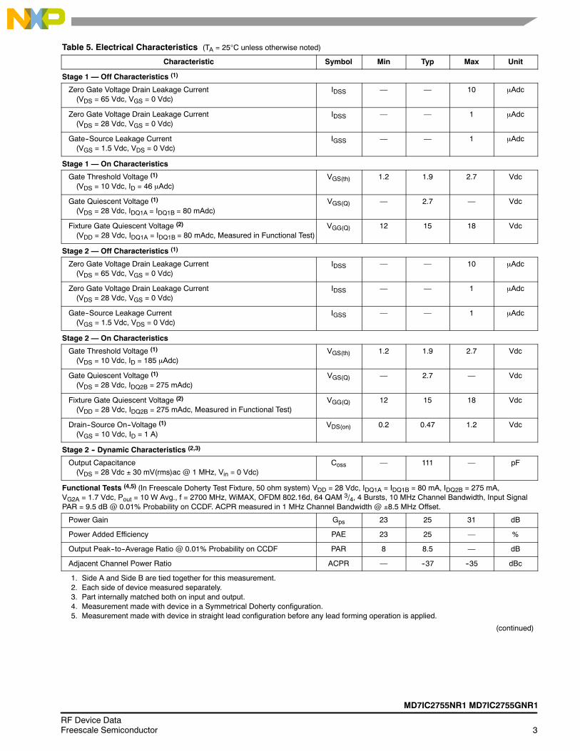
Figure 3. MD7IC2755NR1(GNR1) Test Circuit Schematic
RFINPUT RF
OUTPUT
1
2
3
4
5
8
9
14
12
11
10
DUT
6
7
13
VG2B
Z13 0.0419″ x 0.7690″ MicrostripZ14 0.0717″ x 0.6750″ MicrostripZin 0.0419″ x 1.7230″ MicrostripZout 0.0419″ x 1.1400″ MicrostripPCB Rogers RO4350B, 0.020″, εr = 3.5
Z1, Z2 0.0419″ x 0.480″ MicrostripZ3, Z4 0.247″ x 0.1504″ MicrostripZ5, Z6 0.247″ x 0.1704″ MicrostripZ7, Z8 0.030″ x 0.4400″ MicrostripZ9, Z10 0.0907″ x 0.075″ MicrostripZ11, Z12 0.0419″ x 0.4200″ Microstrip
R12R11R10
C2
C4VG1B
R9R8R7
Z2
Z1R13
VG1AR6R5R4
VG2AR3R2R1
C1
C3C5
C7
C8
C6
Z4
Z3
C9 C11
Z6
Z5
C10 C12
Z10
Z9
C21 C23
C22 C24Quiescent Current
Temperature Compensation
Quiescent CurrentTemperature Compensation
C19
C20
Z12
Z11
Z13
Z14 Zout
Z8
C14
C16
C18
Z7
C17
C15
C13
VDDVD2AVD1A
L2
VD2BVD1B
Zin
SIDE A
SIDE B
L1
COUPLER 1
Table 6. MD7IC2755NR1(GNR1) Test Circuit Component Designations and ValuesPart Description Part Number Manufacturer
C1, C2, C3, C4, C5, C6, C13,C14, C19, C20
6.8 pF Chip Capacitors ATC600S6R8BT250XT ATC
C7, C8, C17, C18 10 μF Chip Capacitors GRM55DR61H106KA88 Murata
C15, C16 1500 pF Chip Capacitors GRM1885C2A152JA01 Murata
C9, C10, C11, C12, C21, C22,C23, C24
0.5 pF Chip Capacitors ATC600S0R5BT250XT ATC
Coupler 1 2500--2700 Hybrid 3 dB Coupler GSC356 Soshin
L1, L2 Jumper Wires
R4, R5, R7, R8 75 Ω, 1/8 W Chip Resistors RK73B2ATTD750G KOA Speer
R1, R10 300 Ω, 1/8 W Chip Resistors RK73B2ATTD301G KOA Speer
R2, R11 2 k Ω, 1/8 W Chip Resistors RK73B2ATTD202G KOA Speer
R3, R6, R9, R12 12 kΩ, 1/8 W Chip Resistors RK73B2ATTD123G KOA Speer
R13 51 Ω, 1/8 W Chip Resistor RK73B2ATTD510G KOA Speer
6RF Device Data
Freescale Semiconductor
MD7IC2755NR1 MD7IC2755GNR1
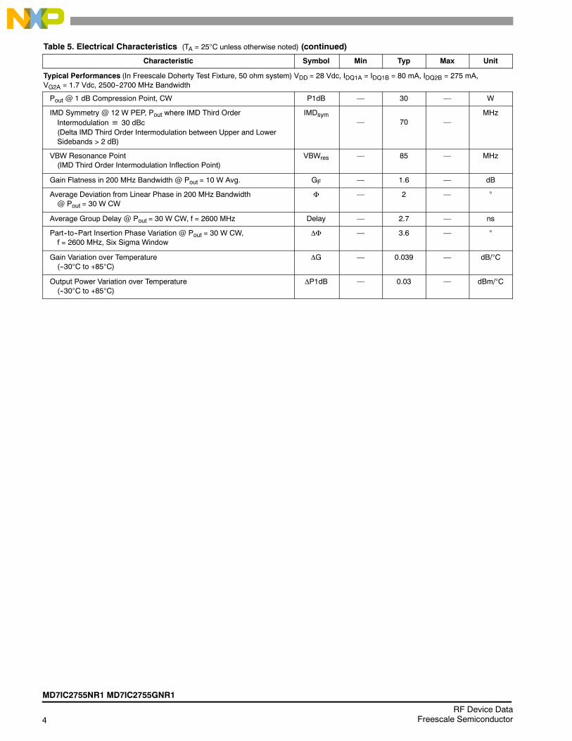
Figure 4. MD7IC2755NR1(GNR1) Test Circuit Component Layout
R1 R2
R4 R5
R3
R6
C7
L2
R13
C5C3
C1
C2
C6C4
R7 R8 R9
R10 R11 R12
C8
L1
C18
C16C14C10 C12
C20
C24C22
C21C23
C19
C17
C15C13
C9 C11VG2A
VG1A
VG1B
VG2B
COUPLER 1
VD1BVD2B
VD2AVD1A MD7IC2755N Rev. 2
P
C
4λ
2
λ
2
λ
4λ
2
λ
2
λ
Single--ended
Quadrature combined
Doherty
Push--pull
4λ4λ 4
λ4λ
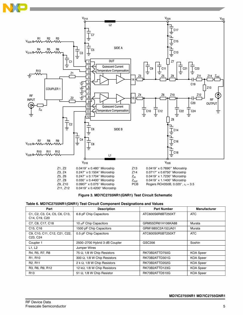
Figure 5. Possible Circuit Topologies
MD7IC2755NR1 MD7IC2755GNR1
7RF Device DataFreescale Semiconductor
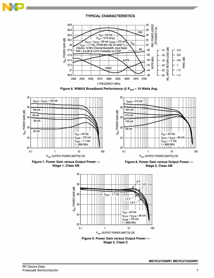
TYPICAL CHARACTERISTICS
IRL,INPUTRETURNLOSS
(dB)
2500
IRL
Gps
ACPR
f, FREQUENCY (MHz)
Figure 6. WiMAX Broadband Performance @ Pout = 10 Watts Avg.
--22
--14
--16
--18
--20
26.8
28.8
28.6
28.4
--46
30
28
26
24
--36
--38
--40
--42
PAE,POWER
ADDED
EFFICIENCY(%)
Gps,POWER
GAIN(dB) 28.2
28
27.6
27.4
27.2
27
2525 2550 2575 2600 2625 2650 2675 2700
22
--44
--24
PARC PARC(dB)
--1.2
--0.4
--0.6
--0.8
--1
--1.4
ACPR
(dBc)
27.8
Figure 7. Power Gain versus Output Power Stage 1, Class AB
22
32
1
IDQ1A = IDQ1B = 120 mA
Pout, OUTPUT POWER (WATTS) CW
40 mA
28
26
10 100
Gps,POWER
GAIN(dB)
30
VDD = 28 VdcIDQ2B = 275 mAVG2A = 1.7 Vdcf = 2600 MHz
24
100 mA
0.1
80 mA
60 mA
Figure 8. Power Gain versus Output Power Stage 2, Class AB
10022
32
1
IDQ2B = 413 mA
344 mA
Pout, OUTPUT POWER (WATTS) CW
95 mA
275 mA
26
10
Gps,POWER
GAIN(dB)
28143 mA
0.1
Figure 9. Power Gain versus Output Power Stage 2, Class C
22
32
1
VG2A = 1.7 Vdc
Pout, OUTPUT POWER (WATTS) CW
26
10 100
Gps,POWER
GAIN(dB)
28
VDD = 28 VdcIDQ1A = IDQ1B = 80 mAIDQ2B = 275 mAf = 2600 MHz
24
1.9 V
0.1
1.6 V1.5 V
VDD = 28 VdcIDQ1A = IDQ1B = 80 mAVG2A = 1.7 Vdcf = 2600 MHz
VG2A = 1.7 Vdc, OFDM 802.16d, 64 QAM 3/44 Bursts, 10 MHz Channel Bandwidth, Input SignalPAR = 9.5 dB @ 0.01% Probability on CCDF
Pout = 10 W (Avg.)
24
30
30 1.8 V
IDQ1A = IDQ1B = 80 mA, IDQ2B = 275 mA
VDD = 28 VdcPAE
8RF Device Data
Freescale Semiconductor
MD7IC2755NR1 MD7IC2755GNR1
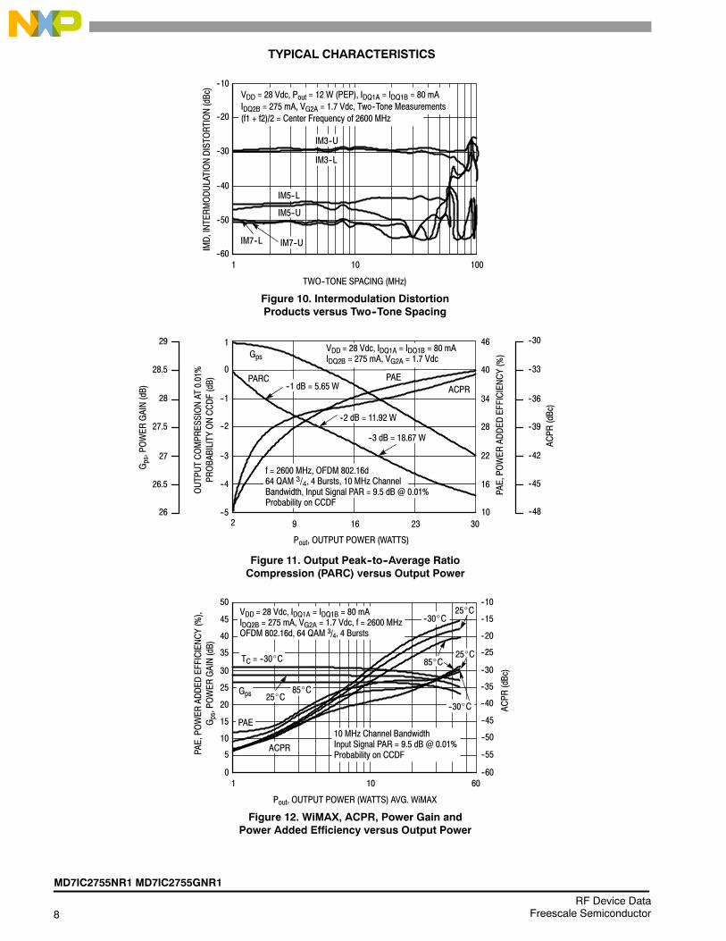
TYPICAL CHARACTERISTICS
Figure 10. Intermodulation DistortionProducts versus Two--Tone Spacing
TWO--TONE SPACING (MHz)
10--60
IM3--U
--20
--30
--50
100
IMD,INTERMODULATIONDISTORTION(dBc)
--40
IM3--L
IM5--U
IM5--L
IM7--L IM7--U
Figure 11. Output Peak--to--Average RatioCompression (PARC) versus Output Power
1
Pout, OUTPUT POWER (WATTS)
--1
--3
--516
--2
--4
OUTPUTCOMPRESSIONAT
0.01%
PROBABILITY
ONCCDF(dB)
2 23 3010
46
34
28
22
16
PAE,POWER
ADDED
EFFICIENCY(%)
ACPRPARC
ACPR
(dBc)
--48
--30
--33
--36
--42
--39
--45
29
Gps,POWER
GAIN(dB)
28.5
26.5
26
Gps
600
50
--60
--10
Pout, OUTPUT POWER (WATTS) AVG. WiMAX
TC = --30_C25_C
85_C
101
40
35
30
25
20
--20
--25
--30
--35
--40 ACPR
(dBc)
Gps
PAE,POWER
ADDED
EFFICIENCY(%),
Gps,POWER
GAIN(dB)
--30_C
25_C
85_C
ACPR
15
10
--45
--50
Figure 12. WiMAX, ACPR, Power Gain andPower Added Efficiency versus Output Power
1
9
40
--1 dB = 5.65 W
--2 dB = 11.92 W
--10
0
28
27.5
27
--3 dB = 18.67 W
5 --55
25_C
--30_C
VDD = 28 Vdc, IDQ1A = IDQ1B = 80 mAIDQ2B = 275 mA, VG2A = 1.7 Vdc
VDD = 28 Vdc, Pout = 12 W (PEP), IDQ1A = IDQ1B = 80 mAIDQ2B = 275 mA, VG2A = 1.7 Vdc, Two--Tone Measurements(f1 + f2)/2 = Center Frequency of 2600 MHz
VDD = 28 Vdc, IDQ1A = IDQ1B = 80 mAIDQ2B = 275 mA, VG2A = 1.7 Vdc, f = 2600 MHzOFDM 802.16d, 64 QAM 3/4, 4 Bursts
PAE
45 --15
10 MHz Channel BandwidthInput Signal PAR = 9.5 dB @ 0.01%Probability on CCDF
f = 2600 MHz, OFDM 802.16d64 QAM 3/4, 4 Bursts, 10 MHz ChannelBandwidth, Input Signal PAR = 9.5 dB @ 0.01%Probability on CCDF
PAE
MD7IC2755NR1 MD7IC2755GNR1
9RF Device DataFreescale Semiconductor
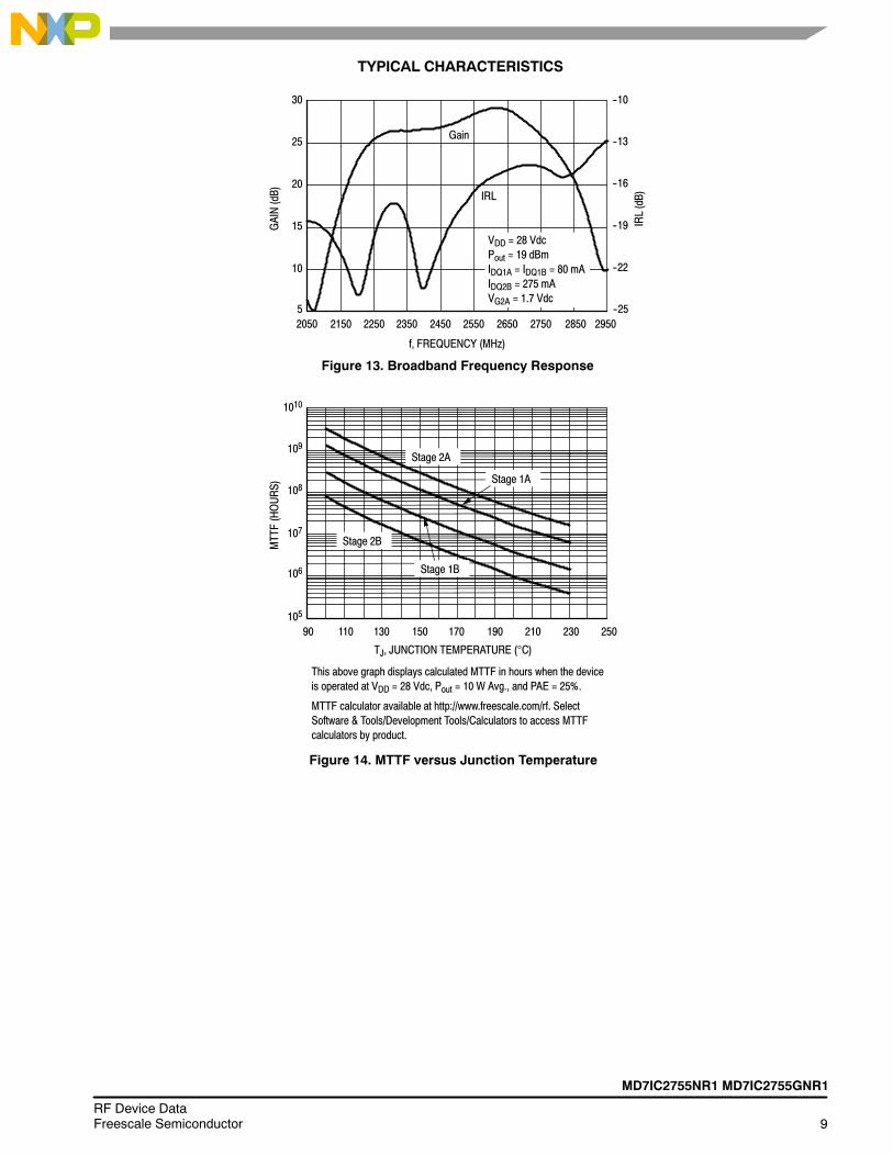
TYPICAL CHARACTERISTICS
29505
30
2050--25
--10
Gain
f, FREQUENCY (MHz)
Figure 13. Broadband Frequency Response
IRL
--1325
--1620
--1915
--2210
26502550245022502150
IRL(dB)
GAIN(dB)
VDD = 28 VdcPout = 19 dBmIDQ1A = IDQ1B = 80 mAIDQ2B = 275 mAVG2A = 1.7 Vdc
2750 28502350
250
1010
90
TJ, JUNCTION TEMPERATURE (°C)
Figure 14. MTTF versus Junction Temperature
This above graph displays calculated MTTF in hours when the deviceis operated at VDD = 28 Vdc, Pout = 10 W Avg., and PAE = 25%.
MTTF calculator available at http://www.freescale.com/rf. SelectSoftware & Tools/Development Tools/Calculators to access MTTFcalculators by product.
108
107
105
110 130 150 170 190
MTTF(HOURS)
210 230
106
109Stage 2A
Stage 1A
Stage 2B
Stage 1B
10RF Device Data
Freescale Semiconductor
MD7IC2755NR1 MD7IC2755GNR1
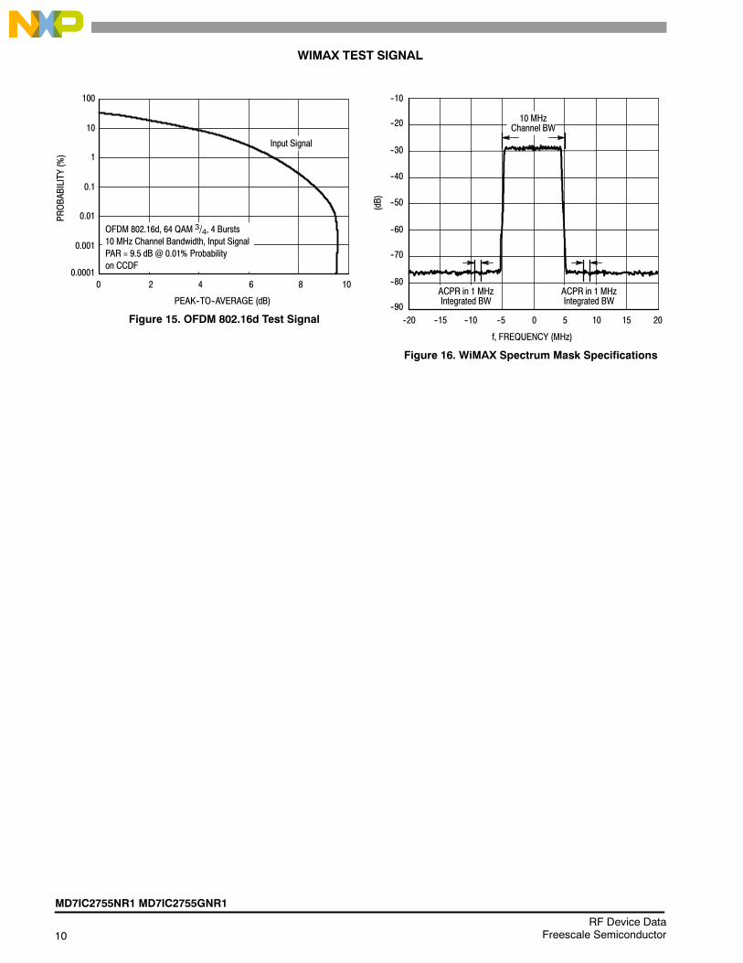
WIMAX TEST SIGNAL
100.0001
100
0
PEAK--TO--AVERAGE (dB)
Figure 15. OFDM 802.16d Test Signal
10
1
0.1
0.01
0.001
2 4 6 8
PROBABILITY
(%)
Input Signal
OFDM 802.16d, 64 QAM 3/4, 4 Bursts10 MHz Channel Bandwidth, Input SignalPAR = 9.5 dB @ 0.01% Probabilityon CCDF
--60
--10
(dB)
--20
--30
--40
--50
--70
--80
--90
10 MHzChannel BW
205 15100--5--10--20
f, FREQUENCY (MHz)
Figure 16. WiMAX Spectrum Mask Specifications
--15
ACPR in 1 MHzIntegrated BW
ACPR in 1 MHzIntegrated BW
Z in
DeviceUnder Test
OutputMatchingNetwork
Z load
DeviceUnder Test
OutputMatchingNetwork
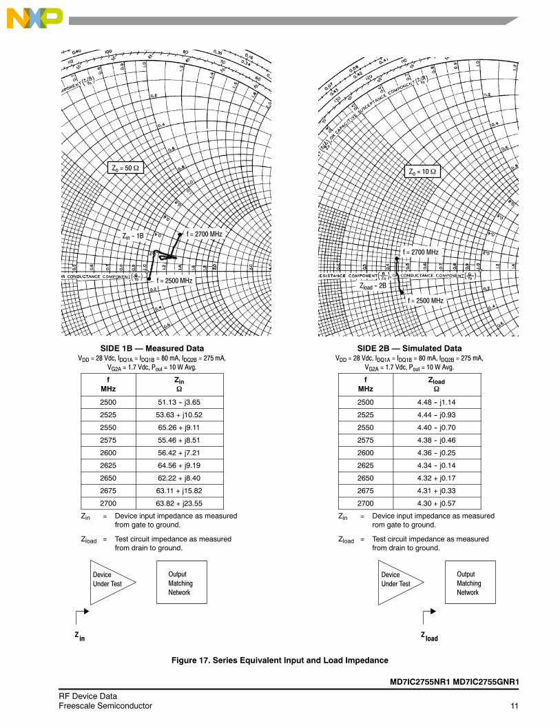
Figure 17. Series Equivalent Input and Load Impedance
MD7IC2755NR1 MD7IC2755GNR1
11RF Device DataFreescale Semiconductor
Zo = 50Ω
Zin -- 1B
f = 2700 MHz
f = 2500 MHz
f = 2700 MHz
f = 2500 MHz
Zo = 10Ω
Zload -- 2B
SIDE 1B Measured DataVDD = 28 Vdc, IDQ1A = IDQ1B = 80 mA, IDQ2B = 275 mA,
VG2A = 1.7 Vdc, Pout = 10 W Avg.
fMHz
ZinΩ
2500 51.13 -- j3.65
2525 53.63 + j10.52
2550 65.26 + j9.11
2575 55.46 + j8.51
2600 56.42 + j7.21
2625 64.56 + j9.19
2650 62.22 + j8.40
2675 63.11 + j15.82
2700 63.82 + j23.55
Zin = Device input impedance as measuredfrom gate to ground.
Zload = Test circuit impedance as measuredfrom drain to ground.
SIDE 2B Simulated DataVDD = 28 Vdc, IDQ1A = IDQ1B = 80 mA, IDQ2B = 275 mA,
VG2A = 1.7 Vdc, Pout = 10 W Avg.
fMHz
ZloadΩ
2500 4.48 -- j1.14
2525 4.44 -- j0.93
2550 4.40 -- j0.70
2575 4.38 -- j0.46
2600 4.36 -- j0.25
2625 4.34 -- j0.14
2650 4.32 + j0.17
2675 4.31 + j0.33
2700 4.30 + j0.57
Zin = Device input impedance as measuredrom gate to ground.
Zload = Test circuit impedance as measuredfrom drain to ground.
12RF Device Data
Freescale Semiconductor
MD7IC2755NR1 MD7IC2755GNR1
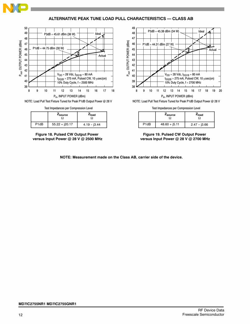
ALTERNATIVE PEAK TUNE LOAD PULL CHARACTERISTICS CLASS AB
18
50
9
P3dB = 45.61 dBm (36 W)
Pin, INPUT POWER (dBm)
48
46
44
42
3910 1211 1413 1715
Actual
Ideal
P1dB = 44.75 dBm (30 W)
49
47
43
45
41
168
P out,OUTPUTPOWER
(dBm
)
NOTE: Load Pull Test Fixture Tuned for Peak P1dB Output Power @ 28 V
VDD = 28 Vdc, IDQ1B = 80 mAIDQ2B = 275 mA, Pulsed CW, 10 μsec(on)10% Duty Cycle, f = 2500 MHz40
Test Impedances per Compression Level
ZsourceΩ
ZloadΩ
P1dB 55.22 + j20.17 4.19 -- j3.44
Figure 18. Pulsed CW Output Powerversus Input Power @ 28 V @ 2500 MHz
209
P3dB = 45.38 dBm (34 W)
Pin, INPUT POWER (dBm)
48
46
44
42
3810 1211 1413 1715
Actual
Ideal
P1dB = 44.31 dBm (27 W)
49
47
43
45
41
168
P out,OUTPUTPOWER
(dBm
)
NOTE: Load Pull Test Fixture Tuned for Peak P1dB Output Power @ 28 V
VDD = 28 Vdc, IDQ1B = 80 mAIDQ2B = 275 mA, Pulsed CW, 10 μsec(on)10% Duty Cycle, f = 2700 MHz
40
39
18 19
Test Impedances per Compression Level
ZsourceΩ
ZloadΩ
P1dB 48.60 + j5.11 2.47 -- j3.66
Figure 19. Pulsed CW Output Powerversus Input Power @ 28 V @ 2700 MHz
NOTE: Measurement made on the Class AB, carrier side of the device.
MD7IC2755NR1 MD7IC2755GNR1
13RF Device DataFreescale Semiconductor
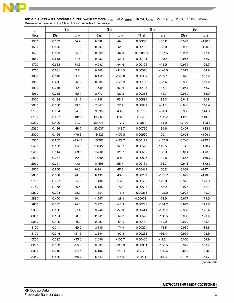
Table 7. Class AB Common Source S--Parameters (VDD = 28 V, IDQ1B = 80 mA, IDQ2B = 275 mA, TA = 25°C, 50 Ohm System)Measurement made on the Class AB, carrier side of the device.
fMHz
S11 S21 S12 S22
|S11| ∠ φ |S21| ∠ φ |S12| ∠ φ |S22| ∠ φ
1500 0.569 74.4 0.002 --64.1 0.00228 135.2 0.997 --176.0
1550 0.575 51.5 0.004 --51.1 0.00100 --30.0 0.997 --179.0
1600 0.593 34.0 0.009 --87.0 0.000590 --107.6 0.995 177.4
1650 0.618 21.8 0.032 --84.4 0.00101 --103.4 0.988 172.7
1700 0.623 14.3 0.092 --94.6 0.00168 --49.5 0.974 166.7
1750 0.601 7.6 0.209 --111.8 0.00326 --146.0 0.979 164.9
1800 0.540 1.5 0.452 --140.8 0.00369 --102.1 0.975 162.2
1850 0.426 --6.8 0.885 --175.9 0.00183 --37.4 0.962 159.2
1900 0.275 --12.9 1.539 151.6 0.00427 --46.1 0.954 156.7
1950 0.058 --69.7 2.773 120.2 0.00351 143.7 0.960 153.0
2000 0.154 121.2 4.188 93.2 0.00632 --82.3 0.946 150.8
2050 0.150 79.4 7.347 72.7 0.00857 --34.1 0.935 146.9
2100 0.064 64.0 9.595 43.3 0.0155 --51.9 0.960 144.0
2150 0.607 --131.3 24.560 26.9 0.0482 --102.7 1.296 110.3
2200 0.406 81.7 28.776 --77.6 0.0257 154.9 0.196 --103.8
2250 0.166 --68.2 22.037 --116.7 0.00750 131.6 0.497 --162.5
2300 0.184 --76.9 19.823 --156.5 0.00936 156.1 0.659 --164.7
2350 0.232 --154.0 16.761 --179.7 0.00172 --139.6 0.743 --173.5
2400 0.182 --94.9 16.827 153.2 0.00578 149.5 0.778 --173.7
2450 0.114 --38.6 15.801 128.7 0.00490 163.9 0.814 --173.9
2500 0.277 --52.4 19.305 89.9 0.00825 142.6 0.853 --169.7
2550 0.261 --3.1 11.891 58.7 0.00185 153.7 0.942 --173.7
2600 0.208 10.3 8.941 47.6 0.00411 166.2 0.961 --177.1
2650 0.568 28.8 8.433 40.6 0.00264 --155.7 0.977 --179.4
2700 0.797 25.0 7.430 15.9 0.00536 128.0 0.976 178.8
2750 0.358 26.5 5.138 --5.8 0.00527 168.2 0.973 177.1
2800 0.384 33.8 4.654 --18.4 0.00311 --178.0 0.976 175.3
2850 0.420 40.4 4.257 --28.4 0.000761 173.9 0.977 173.9
2900 0.337 25.5 3.973 --41.8 0.00233 --134.7 0.977 172.6
2950 0.166 27.4 3.240 --53.3 0.00414 --133.7 0.969 171.4
3000 0.194 23.2 2.641 --52.2 0.00578 --153.5 0.980 170.4
3050 0.186 --9.6 2.337 --61.6 0.00456 158.2 0.979 169.1
3100 0.241 --59.0 2.189 --74.9 0.00204 --78.5 0.982 168.5
3150 0.344 --81.9 2.394 --90.8 0.00281 --98.4 0.974 162.9
3200 0.392 --95.8 2.636 --105.7 0.00468 --122.1 0.966 154.9
3250 0.363 --95.2 3.397 --117.6 0.00661 --106.5 0.949 139.2
3300 0.312 --84.4 5.196 --146.4 0.0170 --126.5 0.819 93.6
3350 0.430 --65.7 5.347 144.0 0.0291 119.3 0.707 --65.7
(continued)

14RF Device Data
Freescale Semiconductor
MD7IC2755NR1 MD7IC2755GNR1
Table 7. Class AB Common Source S--Parameters (VDD = 28 V, IDQ1B = 80 mA, IDQ2B = 275 mA, TA = 25°C, 50 Ohm System)Measurement made on the Class AB, carrier side of the device. (continued)
fMHz
S11 S21 S12 S22
|S11| ∠ φ |S21| ∠ φ |S12| ∠ φ |S22| ∠ φ
3400 0.434 --56.5 2.527 100.7 0.00568 100.1 0.930 --139.3
3450 0.499 --50.1 1.448 92.0 0.00828 25.3 0.865 --161.1
3500 0.546 --52.3 1.394 68.4 0.000298 --87.1 0.944 --163.3
3550 0.518 --56.8 1.073 52.6 0.00543 7.1 0.965 --171.1
3600 0.492 --68.4 0.834 39.8 0.00150 --30.4 0.958 --177.1
MD7IC2755NR1 MD7IC2755GNR1
15RF Device DataFreescale Semiconductor
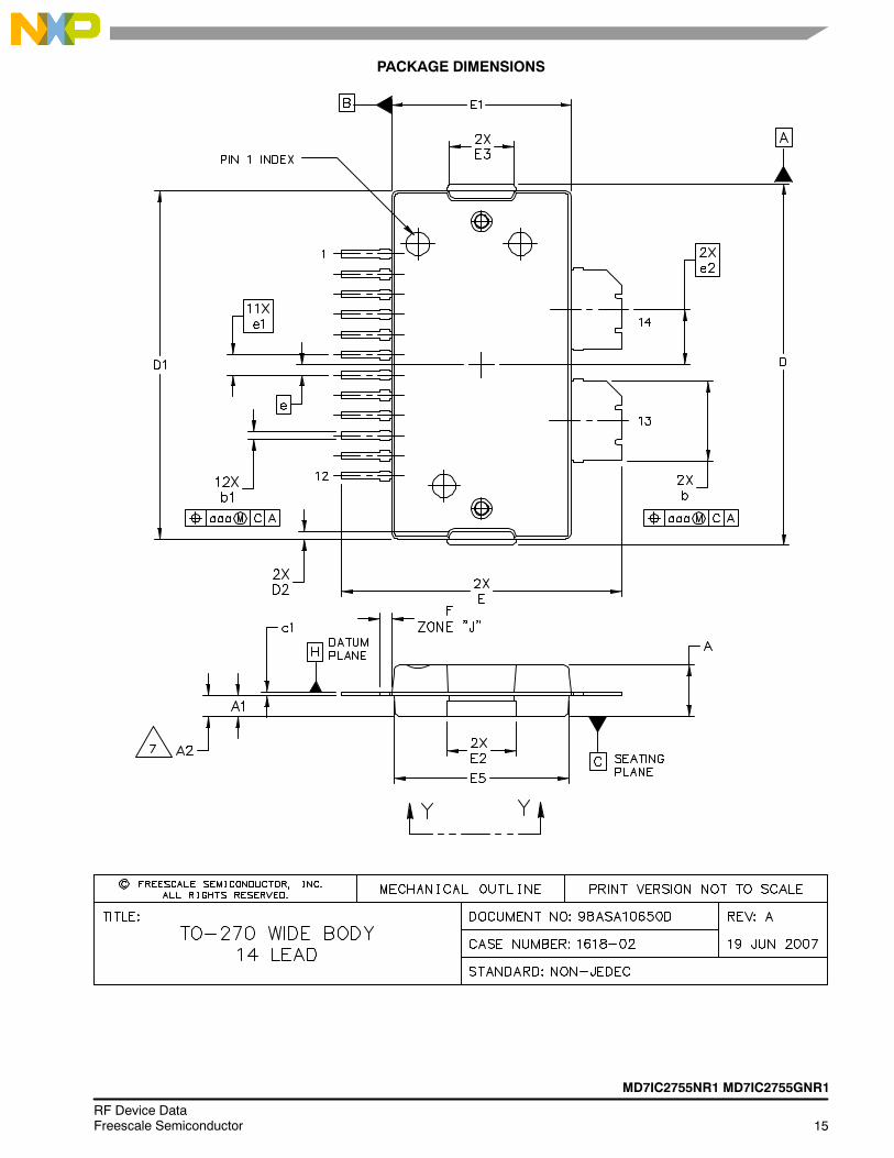
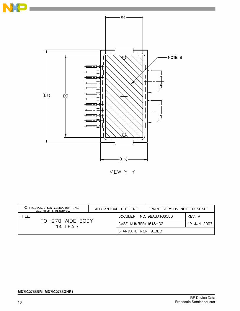
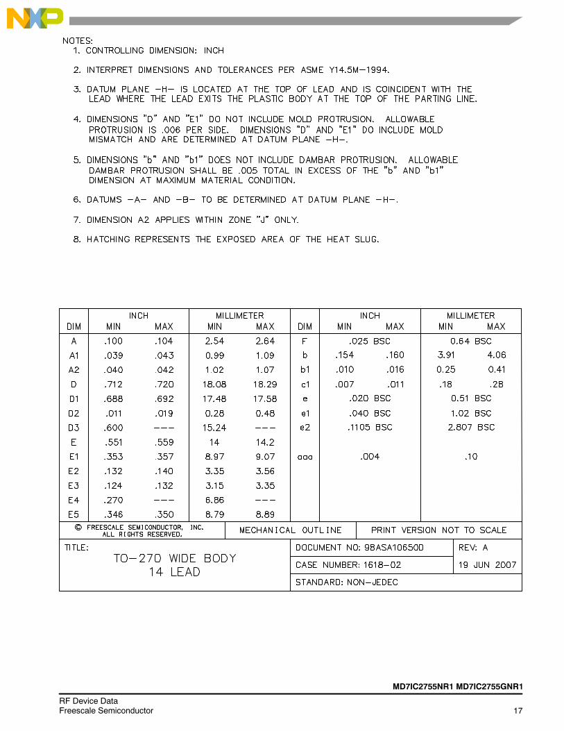
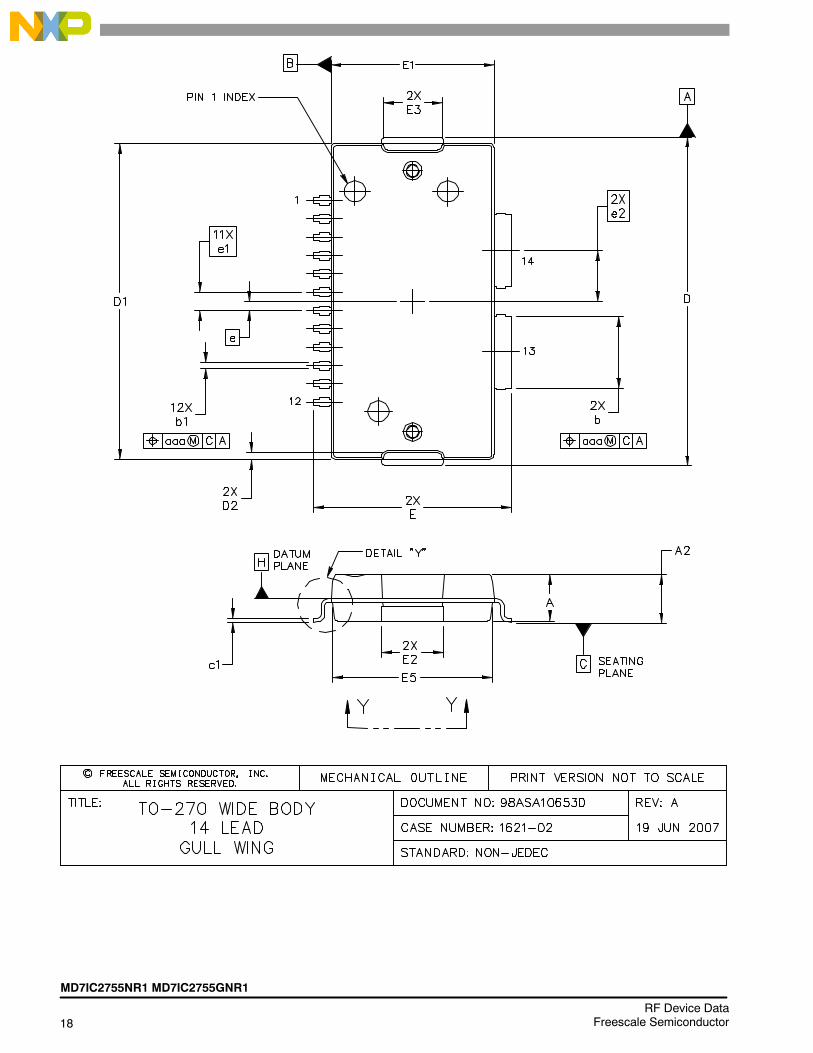
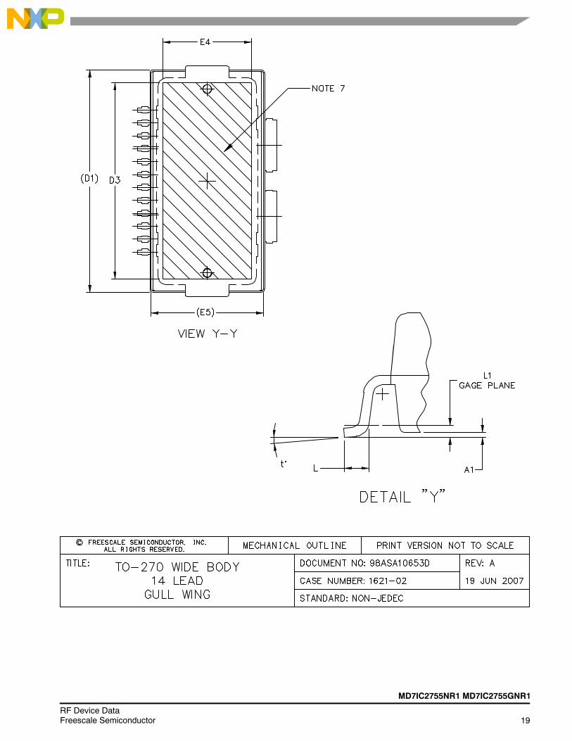
PACKAGE DIMENSIONS
16RF Device Data
Freescale Semiconductor
MD7IC2755NR1 MD7IC2755GNR1
MD7IC2755NR1 MD7IC2755GNR1
17RF Device DataFreescale Semiconductor
18RF Device Data
Freescale Semiconductor
MD7IC2755NR1 MD7IC2755GNR1
MD7IC2755NR1 MD7IC2755GNR1
19RF Device DataFreescale Semiconductor
20RF Device Data
Freescale Semiconductor
MD7IC2755NR1 MD7IC2755GNR1
MD7IC2755NR1 MD7IC2755GNR1
21RF Device DataFreescale Semiconductor
PRODUCT DOCUMENTATION, TOOLS AND SOFTWARE
Refer to the following documents to aid your design process.
Application Notes• AN1907: Solder Reflow Attach Method for High Power RF Devices in Plastic Packages
• AN1955: Thermal Measurement Methodology of RF Power Amplifiers
• AN1977: Quiescent Current Thermal Tracking Circuit in the RF Integrated Circuit Family
• AN1987: Quiescent Current Control for the RF Integrated Circuit Device Family
• AN3263: Bolt Down Mounting Method for High Power RF Transistors and RFICs in Over--Molded Plastic Packages
• AN3789: Clamping of High Power RF Transistors and RFICs in Over--Molded Plastic Packages
Engineering Bulletins• EB212: Using Data Sheet Impedances for RF LDMOS Devices
Software• Electromigration MTTF Calculator
For Software and Tools, do a Part Number search at http://www.freescale.com, and select the Part Number link. Go to theSoftware & Tools tab on the parts Product Summary page to download the respective tool.
REVISION HISTORY
The following table summarizes revisions to this document.
Revision Date Description
0 Jan. 2009 • Initial Release of Data Sheet
1 July 2009 • Test Conditions clarified for Fig. 18, Pulsed CW Output Power versus Input Power @ 28 V @ 2500 MHz,and Fig. 19, Pulsed CW Output Power versus Input Power @ 28 V @ 2700 MHz, p. 12
• Added Electromigration MTTF Calculator availability to Product Software, p. 21
2 Sept. 2010 • For Pout = 10 W CW, changed Stage 1A, Stage 1B thermal resistance values from 4.0 (Stage 1A), 5.0(Stage 1B) to 2.6°C/W and Stage 2A, Stage 2B thermal resistance values from 0.9 (Stage 2A), 2.1(Stage 2B) to 1.8 in Thermal Characteristics table. For Pout = 55 W CW, changed Stage 1A, Stage 1Bthermal resistance values from 4.6 (Stage 1A), 4.2 (Stage 1B) to 2.3°C/W and Stage 2A, Stage 2Bthermal resistance values from 1.2 (Stage 2A), 2.0 (Stage 2B) to 1.1 in Thermal Characteristics table.Thermal value now reflects the use of the combined dissipated power from the carrier amplifier andpeaking amplifier, p. 2.
• Fig. 4, Test Circuit Component Layout, added labels to distinguish Carrier and Peaking side of amplifier,p. 6
3 Sept. 2010 • Fig. 3, Test Circuit Schematic, corrected labeling of C9 and C11 0.5 pF Chip Capacitors, p. 5
22RF Device Data
Freescale Semiconductor
MD7IC2755NR1 MD7IC2755GNR1
Information in this document is provided solely to enable system and softwareimplementers to use Freescale Semiconductor products. There are no express orimplied copyright licenses granted hereunder to design or fabricate any integratedcircuits or integrated circuits based on the information in this document.
Freescale Semiconductor reserves the right to make changes without further notice toany products herein. Freescale Semiconductor makes no warranty, representation orguarantee regarding the suitability of its products for any particular purpose, nor doesFreescale Semiconductor assume any liability arising out of the application or use ofany product or circuit, and specifically disclaims any and all liability, including withoutlimitation consequential or incidental damages. Typical parameters that may beprovided in Freescale Semiconductor data sheets and/or specifications can and dovary in different applications and actual performance may vary over time. All operatingparameters, including Typicals, must be validated for each customer application bycustomers technical experts. Freescale Semiconductor does not convey any licenseunder its patent rights nor the rights of others. Freescale Semiconductor products arenot designed, intended, or authorized for use as components in systems intended forsurgical implant into the body, or other applications intended to support or sustain life,or for any other application in which the failure of the Freescale Semiconductor productcould create a situation where personal injury or death may occur. Should Buyerpurchase or use Freescale Semiconductor products for any such unintended orunauthorized application, Buyer shall indemnify and hold Freescale Semiconductorand its officers, employees, subsidiaries, affiliates, and distributors harmless against allclaims, costs, damages, and expenses, and reasonable attorney fees arising out of,directly or indirectly, any claim of personal injury or death associated with suchunintended or unauthorized use, even if such claim alleges that FreescaleSemiconductor was negligent regarding the design or manufacture of the part.
Freescalet and the Freescale logo are trademarks of Freescale Semiconductor, Inc.All other product or service names are the property of their respective owners.© Freescale Semiconductor, Inc. 2009--2010. All rights reserved.
How to Reach Us:
Home Page:www.freescale.com
Web Support:http://www.freescale.com/support
USA/Europe or Locations Not Listed:Freescale Semiconductor, Inc.Technical Information Center, EL5162100 East Elliot RoadTempe, Arizona 852841--800--521--6274 or +1--480--768--2130www.freescale.com/support
Europe, Middle East, and Africa:Freescale Halbleiter Deutschland GmbHTechnical Information CenterSchatzbogen 781829 Muenchen, Germany+44 1296 380 456 (English)+46 8 52200080 (English)+49 89 92103 559 (German)+33 1 69 35 48 48 (French)www.freescale.com/support
Japan:Freescale Semiconductor Japan Ltd.HeadquartersARCO Tower 15F1--8--1, Shimo--Meguro, Meguro--ku,Tokyo 153--0064Japan0120 191014 or +81 3 5437 [email protected]
Asia/Pacific:Freescale Semiconductor China Ltd.Exchange Building 23FNo. 118 Jianguo RoadChaoyang DistrictBeijing 100022China+86 10 5879 [email protected]
For Literature Requests Only:Freescale Semiconductor Literature Distribution Center1--800--441--2447 or +1--303--675--2140Fax: [email protected]
Document Number: MD7IC2755NRev. 3, 9/2010


![Network Working Group J. Sjoberg Wideband (AMR-WB) … · · 2005-11-23The Adaptive Multi-Rate Wideband (AMR-WB) speech codec [3] was originally developed by 3GPP to be used in](https://img.pdfslide.us/doc/110x75/5ac12ce67f8b9a1c768c81c0/network-working-group-j-sjoberg-wideband-amr-wb-adaptive-multi-rate-wideband.jpg)