Embed Size (px)
Citation preview
September 2013 Doc ID 13311 Rev 5 1/61
1
TDA7529
RF front-end for AM/FM DSP car-radio with IF sampling
Features■ Fully integrated VCO for world tuning
■ High performance PLL for fast RDS system
■ I/Q mixer for FM IF 10.7 MHz with image rejection and integrated LNA
■ I/Q mixer for AM IF 10.7 MHz up conversion with high dynamic range
■ Integrated balun, which allows saving of external mixer tank
■ RF AGC, IF AGC, DAGC
■ Low noise IF amplifier with switched wide dynamic AGC range
■ IF switch for FM / AM / IBOC
■ Electronic alignment for the preselection stages
■ I2C/SPI controlled
■ Single 5 V supply
■ Alternative frequency control signals to DSP
DescriptionThe front-end is a high performance tuner circuit for AM/FM - DSP car-radios with 10.7 MHz IF sampling. It contains mixer and IF amplifiers for AM and FM, fully integrated VCO and PLL synthesizer on a single chip. Use of BiCMOS technology allows the implementation of several tuning functions and a minimum of external components.
LQFP64
Table 1. Device summary
Order code Package Packing
TDA7529TX LQFP64 exposed pad (10x10x1.4) Tape and reel
www.st.com
Contents TDA7529
2/61 Doc ID 13311 Rev 5
Contents
1 Functional block diagram . . . . . . . . . . . . . . . . . . . . . . . . . . . . . . . . . . . . . 8
2 Pin description . . . . . . . . . . . . . . . . . . . . . . . . . . . . . . . . . . . . . . . . . . . . . 9
3 Function description . . . . . . . . . . . . . . . . . . . . . . . . . . . . . . . . . . . . . . . . 12
3.1 IMR mixer and active balun output . . . . . . . . . . . . . . . . . . . . . . . . . . . . . . 12
3.2 FM RF-AGC . . . . . . . . . . . . . . . . . . . . . . . . . . . . . . . . . . . . . . . . . . . . . . . 12
3.3 AM RF-AGC . . . . . . . . . . . . . . . . . . . . . . . . . . . . . . . . . . . . . . . . . . . . . . . 13
3.4 IF AGC and IF amplifier . . . . . . . . . . . . . . . . . . . . . . . . . . . . . . . . . . . . . . 14
3.5 Dividers . . . . . . . . . . . . . . . . . . . . . . . . . . . . . . . . . . . . . . . . . . . . . . . . . . 14
3.6 D/A converters . . . . . . . . . . . . . . . . . . . . . . . . . . . . . . . . . . . . . . . . . . . . . 14
3.7 VCO . . . . . . . . . . . . . . . . . . . . . . . . . . . . . . . . . . . . . . . . . . . . . . . . . . . . . 15
3.8 FREF . . . . . . . . . . . . . . . . . . . . . . . . . . . . . . . . . . . . . . . . . . . . . . . . . . . . 15
3.9 A/D converter . . . . . . . . . . . . . . . . . . . . . . . . . . . . . . . . . . . . . . . . . . . . . . 15
3.10 GPIO - general purpose IO interface pins . . . . . . . . . . . . . . . . . . . . . . . . 16
3.11 AFSAMPLE/AFHOLD . . . . . . . . . . . . . . . . . . . . . . . . . . . . . . . . . . . . . . . . 17
3.12 Serial bus interface . . . . . . . . . . . . . . . . . . . . . . . . . . . . . . . . . . . . . . . . . . 17
4 Electrical specifications . . . . . . . . . . . . . . . . . . . . . . . . . . . . . . . . . . . . . 19
4.1 Absolute maximum ratings . . . . . . . . . . . . . . . . . . . . . . . . . . . . . . . . . . . . 19
4.2 Thermal data . . . . . . . . . . . . . . . . . . . . . . . . . . . . . . . . . . . . . . . . . . . . . . 19
4.3 General key parameters . . . . . . . . . . . . . . . . . . . . . . . . . . . . . . . . . . . . . . 19
4.4 FM - section . . . . . . . . . . . . . . . . . . . . . . . . . . . . . . . . . . . . . . . . . . . . . . . 20
4.5 AM - section . . . . . . . . . . . . . . . . . . . . . . . . . . . . . . . . . . . . . . . . . . . . . . . 21
4.6 IF - section . . . . . . . . . . . . . . . . . . . . . . . . . . . . . . . . . . . . . . . . . . . . . . . . 22
4.7 VCO . . . . . . . . . . . . . . . . . . . . . . . . . . . . . . . . . . . . . . . . . . . . . . . . . . . . . 24
4.8 Reference frequency input buffer . . . . . . . . . . . . . . . . . . . . . . . . . . . . . . . 24
4.9 Dividers . . . . . . . . . . . . . . . . . . . . . . . . . . . . . . . . . . . . . . . . . . . . . . . . . . 24
4.10 Phase locked loop . . . . . . . . . . . . . . . . . . . . . . . . . . . . . . . . . . . . . . . . . . 25
4.11 Phase frequency detector and charge pump . . . . . . . . . . . . . . . . . . . . . . 25
4.12 Temperature sensor . . . . . . . . . . . . . . . . . . . . . . . . . . . . . . . . . . . . . . . . . 26
4.13 D/A-converter . . . . . . . . . . . . . . . . . . . . . . . . . . . . . . . . . . . . . . . . . . . . . . 26
TDA7529 Contents
Doc ID 13311 Rev 5 3/61
4.14 A/D-converter . . . . . . . . . . . . . . . . . . . . . . . . . . . . . . . . . . . . . . . . . . . . . . 26
4.15 GPIO – general purpose IO interface pins . . . . . . . . . . . . . . . . . . . . . . . . 27
4.16 AFSAMPLE / AFHOLD . . . . . . . . . . . . . . . . . . . . . . . . . . . . . . . . . . . . . . . 27
4.17 Serial data interface . . . . . . . . . . . . . . . . . . . . . . . . . . . . . . . . . . . . . . . . . 28
5 Tuning state machine . . . . . . . . . . . . . . . . . . . . . . . . . . . . . . . . . . . . . . . 29
5.1 Tuning state machine modes . . . . . . . . . . . . . . . . . . . . . . . . . . . . . . . . . . 29
5.1.1 Mode 000: buffer (nil) . . . . . . . . . . . . . . . . . . . . . . . . . . . . . . . . . . . . . . . 29
5.1.2 Mode 001: preset . . . . . . . . . . . . . . . . . . . . . . . . . . . . . . . . . . . . . . . . . . 29
5.1.3 Mode 010: search . . . . . . . . . . . . . . . . . . . . . . . . . . . . . . . . . . . . . . . . . 30
5.1.4 Mode 011: AF update . . . . . . . . . . . . . . . . . . . . . . . . . . . . . . . . . . . . . . 30
5.1.5 Mode 100: jump . . . . . . . . . . . . . . . . . . . . . . . . . . . . . . . . . . . . . . . . . . . 31
5.2 Mode 100: check . . . . . . . . . . . . . . . . . . . . . . . . . . . . . . . . . . . . . . . . . . . 31
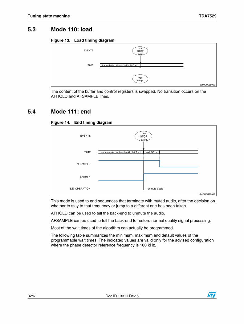
5.3 Mode 110: load . . . . . . . . . . . . . . . . . . . . . . . . . . . . . . . . . . . . . . . . . . . . 32
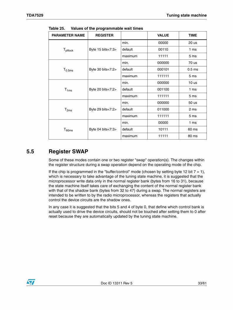
5.4 Mode 111: end . . . . . . . . . . . . . . . . . . . . . . . . . . . . . . . . . . . . . . . . . . . . . 32
5.5 Register SWAP . . . . . . . . . . . . . . . . . . . . . . . . . . . . . . . . . . . . . . . . . . . . 33
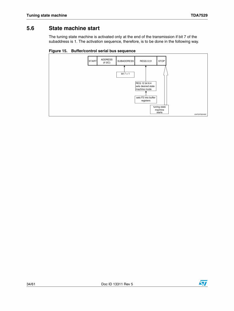
5.6 State machine start . . . . . . . . . . . . . . . . . . . . . . . . . . . . . . . . . . . . . . . . . 34
6 Registers description . . . . . . . . . . . . . . . . . . . . . . . . . . . . . . . . . . . . . . . 35
6.1 Data byte specification . . . . . . . . . . . . . . . . . . . . . . . . . . . . . . . . . . . . . . . 37
6.1.1 Short_reg (0) . . . . . . . . . . . . . . . . . . . . . . . . . . . . . . . . . . . . . . . . . . . . . 37
6.1.2 ADCctrl (1) . . . . . . . . . . . . . . . . . . . . . . . . . . . . . . . . . . . . . . . . . . . . . . . 38
6.1.3 GPIO mode (2) . . . . . . . . . . . . . . . . . . . . . . . . . . . . . . . . . . . . . . . . . . . 39
6.1.4 AGC and mixer control (3) . . . . . . . . . . . . . . . . . . . . . . . . . . . . . . . . . . . 40
6.1.5 Register (4) . . . . . . . . . . . . . . . . . . . . . . . . . . . . . . . . . . . . . . . . . . . . . . 41
6.1.6 Divider R (5) . . . . . . . . . . . . . . . . . . . . . . . . . . . . . . . . . . . . . . . . . . . . . . 41
6.1.7 IF AGC control (6) . . . . . . . . . . . . . . . . . . . . . . . . . . . . . . . . . . . . . . . . . 42
6.1.8 FM AGC (7) . . . . . . . . . . . . . . . . . . . . . . . . . . . . . . . . . . . . . . . . . . . . . . 43
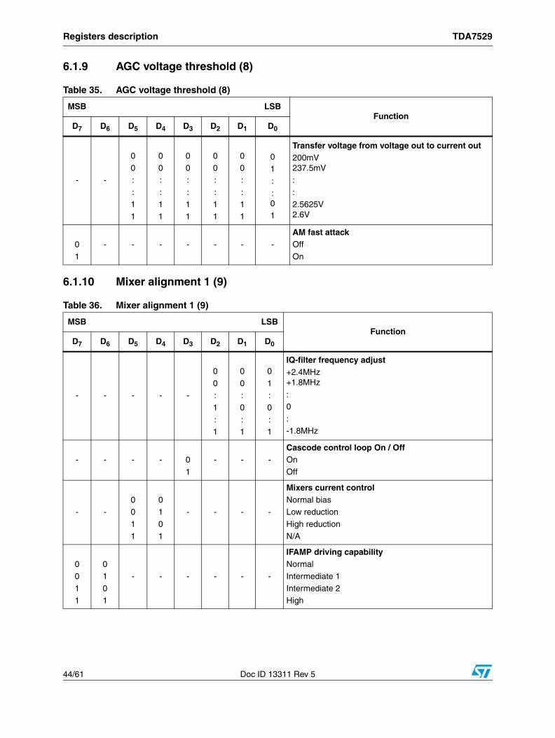
6.1.9 AGC voltage threshold (8) . . . . . . . . . . . . . . . . . . . . . . . . . . . . . . . . . . . 44
6.1.10 Mixer alignment 1 (9) . . . . . . . . . . . . . . . . . . . . . . . . . . . . . . . . . . . . . . . 44
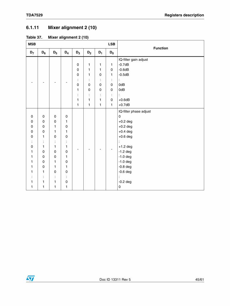
6.1.11 Mixer alignment 2 (10) . . . . . . . . . . . . . . . . . . . . . . . . . . . . . . . . . . . . . . 45
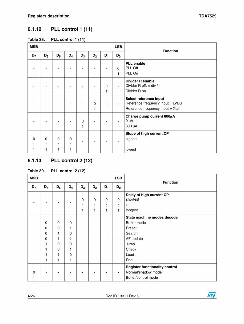
6.1.12 PLL control 1 (11) . . . . . . . . . . . . . . . . . . . . . . . . . . . . . . . . . . . . . . . . . 46
6.1.13 PLL control 2 (12) . . . . . . . . . . . . . . . . . . . . . . . . . . . . . . . . . . . . . . . . . 46
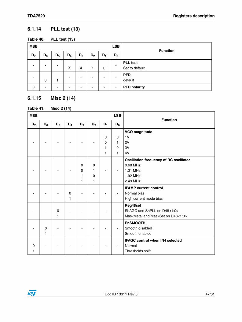
6.1.14 PLL test (13) . . . . . . . . . . . . . . . . . . . . . . . . . . . . . . . . . . . . . . . . . . . . . 47
6.1.15 Misc 2 (14) . . . . . . . . . . . . . . . . . . . . . . . . . . . . . . . . . . . . . . . . . . . . . . . 47
6.1.16 Wait lock (15) . . . . . . . . . . . . . . . . . . . . . . . . . . . . . . . . . . . . . . . . . . . . . 48
Contents TDA7529
4/61 Doc ID 13311 Rev 5
6.1.17 AGC time constant settings (16 / 32) . . . . . . . . . . . . . . . . . . . . . . . . . . . 48
6.1.18 AMAGC control (17 / 33) . . . . . . . . . . . . . . . . . . . . . . . . . . . . . . . . . . . . 49
6.1.19 GPIO output level control (18 / 34) . . . . . . . . . . . . . . . . . . . . . . . . . . . . 50
6.1.20 IF control (19 / 35) . . . . . . . . . . . . . . . . . . . . . . . . . . . . . . . . . . . . . . . . . 50
6.1.21 AF state machine wait time 1 (20 / 36) . . . . . . . . . . . . . . . . . . . . . . . . . 51
6.1.22 PLL main divider (N-divider) 1 (21 / 37) . . . . . . . . . . . . . . . . . . . . . . . . . 51
6.1.23 PLL main divider (N-divider) 2 (22 / 38) . . . . . . . . . . . . . . . . . . . . . . . . . 51
6.1.24 PLL main divider (N-divider) 3 (23 / 39) . . . . . . . . . . . . . . . . . . . . . . . . . 52
6.1.25 PLL Divider ratio calculation . . . . . . . . . . . . . . . . . . . . . . . . . . . . . . . . . 52
6.1.26 VCO divider (V-divider) (24 / 40) . . . . . . . . . . . . . . . . . . . . . . . . . . . . . . 52
6.1.27 Charge pump current (25 / 41) . . . . . . . . . . . . . . . . . . . . . . . . . . . . . . . 53
6.1.28 Tuning DAC 1 (26 / 42) . . . . . . . . . . . . . . . . . . . . . . . . . . . . . . . . . . . . . . 53
6.1.29 Tuning DAC 2 (27 / 43) . . . . . . . . . . . . . . . . . . . . . . . . . . . . . . . . . . . . . . 54
6.1.30 Different controls (28 / 44) . . . . . . . . . . . . . . . . . . . . . . . . . . . . . . . . . . . 54
6.1.31 Misc 3 (29 / 45) . . . . . . . . . . . . . . . . . . . . . . . . . . . . . . . . . . . . . . . . . . . 55
6.1.32 Analog test select (30 / 46) . . . . . . . . . . . . . . . . . . . . . . . . . . . . . . . . . . 55
6.1.33 AD converter test (31 / 47) . . . . . . . . . . . . . . . . . . . . . . . . . . . . . . . . . . . 56
6.1.34 Read 1 (48) . . . . . . . . . . . . . . . . . . . . . . . . . . . . . . . . . . . . . . . . . . . . . . 56
6.1.35 Read 2 (49) . . . . . . . . . . . . . . . . . . . . . . . . . . . . . . . . . . . . . . . . . . . . . . 57
7 Application schematic . . . . . . . . . . . . . . . . . . . . . . . . . . . . . . . . . . . . . . 58
8 Package information . . . . . . . . . . . . . . . . . . . . . . . . . . . . . . . . . . . . . . . . 59
9 Revision history . . . . . . . . . . . . . . . . . . . . . . . . . . . . . . . . . . . . . . . . . . . 60
TDA7529 List of tables
Doc ID 13311 Rev 5 5/61
List of tables
Table 1. Device summary . . . . . . . . . . . . . . . . . . . . . . . . . . . . . . . . . . . . . . . . . . . . . . . . . . . . . . . . . . 1Table 2. Pin assignment . . . . . . . . . . . . . . . . . . . . . . . . . . . . . . . . . . . . . . . . . . . . . . . . . . . . . . . . . . . 9Table 3. IF AGC and IF amplifier . . . . . . . . . . . . . . . . . . . . . . . . . . . . . . . . . . . . . . . . . . . . . . . . . . . 14Table 4. Switching frequency as a function of the process. . . . . . . . . . . . . . . . . . . . . . . . . . . . . . . . 15Table 5. GPIO - general purpose IO interface pins . . . . . . . . . . . . . . . . . . . . . . . . . . . . . . . . . . . . . 16Table 6. Supports data communication using the SPI and the I2C protocol . . . . . . . . . . . . . . . . . . . 17Table 7. I2C addresses . . . . . . . . . . . . . . . . . . . . . . . . . . . . . . . . . . . . . . . . . . . . . . . . . . . . . . . . . . . 18Table 8. Absolute maximum ratings . . . . . . . . . . . . . . . . . . . . . . . . . . . . . . . . . . . . . . . . . . . . . . . . . 19Table 9. Thermal data. . . . . . . . . . . . . . . . . . . . . . . . . . . . . . . . . . . . . . . . . . . . . . . . . . . . . . . . . . . . 19Table 10. General key parameters . . . . . . . . . . . . . . . . . . . . . . . . . . . . . . . . . . . . . . . . . . . . . . . . . . . 19Table 11. FM - section . . . . . . . . . . . . . . . . . . . . . . . . . . . . . . . . . . . . . . . . . . . . . . . . . . . . . . . . . . . . 20Table 12. AM - section . . . . . . . . . . . . . . . . . . . . . . . . . . . . . . . . . . . . . . . . . . . . . . . . . . . . . . . . . . . . 21Table 13. IF - section . . . . . . . . . . . . . . . . . . . . . . . . . . . . . . . . . . . . . . . . . . . . . . . . . . . . . . . . . . . . . 22Table 14. VCO . . . . . . . . . . . . . . . . . . . . . . . . . . . . . . . . . . . . . . . . . . . . . . . . . . . . . . . . . . . . . . . . . . 24Table 15. Reference frequency input buffer . . . . . . . . . . . . . . . . . . . . . . . . . . . . . . . . . . . . . . . . . . . . 24Table 16. Dividers. . . . . . . . . . . . . . . . . . . . . . . . . . . . . . . . . . . . . . . . . . . . . . . . . . . . . . . . . . . . . . . . 24Table 17. Phase Locked Loop . . . . . . . . . . . . . . . . . . . . . . . . . . . . . . . . . . . . . . . . . . . . . . . . . . . . . . 25Table 18. Phase frequency detector and charge pump . . . . . . . . . . . . . . . . . . . . . . . . . . . . . . . . . . . 25Table 19. Temperature sensor . . . . . . . . . . . . . . . . . . . . . . . . . . . . . . . . . . . . . . . . . . . . . . . . . . . . . . 26Table 20. D/A-converter . . . . . . . . . . . . . . . . . . . . . . . . . . . . . . . . . . . . . . . . . . . . . . . . . . . . . . . . . . . 26Table 21. A/D-converter . . . . . . . . . . . . . . . . . . . . . . . . . . . . . . . . . . . . . . . . . . . . . . . . . . . . . . . . . . . 26Table 22. GPIO - general purpose IO interface pins . . . . . . . . . . . . . . . . . . . . . . . . . . . . . . . . . . . . . 27Table 23. AFSAMPLE / AFHOLD . . . . . . . . . . . . . . . . . . . . . . . . . . . . . . . . . . . . . . . . . . . . . . . . . . . . 27Table 24. Serial data interface . . . . . . . . . . . . . . . . . . . . . . . . . . . . . . . . . . . . . . . . . . . . . . . . . . . . . . 28Table 25. Values of the programmable wait times . . . . . . . . . . . . . . . . . . . . . . . . . . . . . . . . . . . . . . . 33Table 26. Registers description . . . . . . . . . . . . . . . . . . . . . . . . . . . . . . . . . . . . . . . . . . . . . . . . . . . . . 35Table 27. Short_reg (0). . . . . . . . . . . . . . . . . . . . . . . . . . . . . . . . . . . . . . . . . . . . . . . . . . . . . . . . . . . . 37Table 28. ADCctrl (1) . . . . . . . . . . . . . . . . . . . . . . . . . . . . . . . . . . . . . . . . . . . . . . . . . . . . . . . . . . . . . 38Table 29. GPIO mode (2) . . . . . . . . . . . . . . . . . . . . . . . . . . . . . . . . . . . . . . . . . . . . . . . . . . . . . . . . . . 39Table 30. AGC and mixer control (3 . . . . . . . . . . . . . . . . . . . . . . . . . . . . . . . . . . . . . . . . . . . . . . . . . . 40Table 31. Register (4) . . . . . . . . . . . . . . . . . . . . . . . . . . . . . . . . . . . . . . . . . . . . . . . . . . . . . . . . . . . . . 41Table 32. Divider R (5) . . . . . . . . . . . . . . . . . . . . . . . . . . . . . . . . . . . . . . . . . . . . . . . . . . . . . . . . . . . . 41Table 33. IF AGC control (6). . . . . . . . . . . . . . . . . . . . . . . . . . . . . . . . . . . . . . . . . . . . . . . . . . . . . . . . 42Table 34. FM AGC (7) . . . . . . . . . . . . . . . . . . . . . . . . . . . . . . . . . . . . . . . . . . . . . . . . . . . . . . . . . . . . 43Table 35. AGC voltage threshold (8) . . . . . . . . . . . . . . . . . . . . . . . . . . . . . . . . . . . . . . . . . . . . . . . . . 44Table 36. Mixer alignment 1 (9) . . . . . . . . . . . . . . . . . . . . . . . . . . . . . . . . . . . . . . . . . . . . . . . . . . . . . 44Table 37. Mixer alignment 2 (10) . . . . . . . . . . . . . . . . . . . . . . . . . . . . . . . . . . . . . . . . . . . . . . . . . . . . 45Table 38. PLL control 1 (11) . . . . . . . . . . . . . . . . . . . . . . . . . . . . . . . . . . . . . . . . . . . . . . . . . . . . . . . . 46Table 39. PLL control 2 (12) . . . . . . . . . . . . . . . . . . . . . . . . . . . . . . . . . . . . . . . . . . . . . . . . . . . . . . . . 46Table 40. PLL test (13) . . . . . . . . . . . . . . . . . . . . . . . . . . . . . . . . . . . . . . . . . . . . . . . . . . . . . . . . . . . . 47Table 41. Misc 2 (14) . . . . . . . . . . . . . . . . . . . . . . . . . . . . . . . . . . . . . . . . . . . . . . . . . . . . . . . . . . . . . 47Table 42. Wait lock (15) . . . . . . . . . . . . . . . . . . . . . . . . . . . . . . . . . . . . . . . . . . . . . . . . . . . . . . . . . . . 48Table 43. AGC time constant settings (16 / 32) . . . . . . . . . . . . . . . . . . . . . . . . . . . . . . . . . . . . . . . . . 48Table 44. AMAGC control (17 / 33 . . . . . . . . . . . . . . . . . . . . . . . . . . . . . . . . . . . . . . . . . . . . . . . . . . . 49Table 45. GPIO output level control (18 / 34) . . . . . . . . . . . . . . . . . . . . . . . . . . . . . . . . . . . . . . . . . . . 50Table 46. IF control (19 / 35) . . . . . . . . . . . . . . . . . . . . . . . . . . . . . . . . . . . . . . . . . . . . . . . . . . . . . . . 50Table 47. AF state machine wait time 1 (20 / 36) . . . . . . . . . . . . . . . . . . . . . . . . . . . . . . . . . . . . . . . . 51Table 48. PLL main divider (N-divider) 1 (21 / 37) . . . . . . . . . . . . . . . . . . . . . . . . . . . . . . . . . . . . . . . 51
List of tables TDA7529
6/61 Doc ID 13311 Rev 5
Table 49. PLL main divider (N-divider) 2 (22 / 38) . . . . . . . . . . . . . . . . . . . . . . . . . . . . . . . . . . . . . . . 51Table 50. PLL main divider (N-divider) 3 (23 / 39) . . . . . . . . . . . . . . . . . . . . . . . . . . . . . . . . . . . . . . . 52Table 51. PLL Divider ratio calculation . . . . . . . . . . . . . . . . . . . . . . . . . . . . . . . . . . . . . . . . . . . . . . . . 52Table 52. VCO divider (V-divider) (24 / 40) . . . . . . . . . . . . . . . . . . . . . . . . . . . . . . . . . . . . . . . . . . . . 52Table 53. Charge pump current (25 / 41) . . . . . . . . . . . . . . . . . . . . . . . . . . . . . . . . . . . . . . . . . . . . . . 53Table 54. Tuning DAC 1 (26 / 42) . . . . . . . . . . . . . . . . . . . . . . . . . . . . . . . . . . . . . . . . . . . . . . . . . . . . 53Table 55. Tuning DAC 2 (27 / 43) . . . . . . . . . . . . . . . . . . . . . . . . . . . . . . . . . . . . . . . . . . . . . . . . . . . . 54Table 56. Different controls (28 / 44) . . . . . . . . . . . . . . . . . . . . . . . . . . . . . . . . . . . . . . . . . . . . . . . . . 54Table 57. Misc 3 (29 / 45) . . . . . . . . . . . . . . . . . . . . . . . . . . . . . . . . . . . . . . . . . . . . . . . . . . . . . . . . . . 55Table 58. Analog test select (30 / 46) . . . . . . . . . . . . . . . . . . . . . . . . . . . . . . . . . . . . . . . . . . . . . . . . . 55Table 59. AD converter test (31 / 47) . . . . . . . . . . . . . . . . . . . . . . . . . . . . . . . . . . . . . . . . . . . . . . . . . 56Table 60. Read 1 (48) . . . . . . . . . . . . . . . . . . . . . . . . . . . . . . . . . . . . . . . . . . . . . . . . . . . . . . . . . . . . . 56Table 61. Read 2 (49) . . . . . . . . . . . . . . . . . . . . . . . . . . . . . . . . . . . . . . . . . . . . . . . . . . . . . . . . . . . . . 57Table 62. Document revision history . . . . . . . . . . . . . . . . . . . . . . . . . . . . . . . . . . . . . . . . . . . . . . . . . 60
TDA7529 List of figures
Doc ID 13311 Rev 5 7/61
List of figures
Figure 1. Functional block diagram . . . . . . . . . . . . . . . . . . . . . . . . . . . . . . . . . . . . . . . . . . . . . . . . . . . 8Figure 2. Pin connection . . . . . . . . . . . . . . . . . . . . . . . . . . . . . . . . . . . . . . . . . . . . . . . . . . . . . . . . . . . 9Figure 3. Positive current diagram . . . . . . . . . . . . . . . . . . . . . . . . . . . . . . . . . . . . . . . . . . . . . . . . . . . 12Figure 4. Positive/negative current diagram . . . . . . . . . . . . . . . . . . . . . . . . . . . . . . . . . . . . . . . . . . . 13Figure 5. Voltage and current mode with hand-over . . . . . . . . . . . . . . . . . . . . . . . . . . . . . . . . . . . . . 13Figure 6. I2C (sub address mode) . . . . . . . . . . . . . . . . . . . . . . . . . . . . . . . . . . . . . . . . . . . . . . . . . . . 18Figure 7. SPI . . . . . . . . . . . . . . . . . . . . . . . . . . . . . . . . . . . . . . . . . . . . . . . . . . . . . . . . . . . . . . . . . . . 18Figure 8. Preset timing diagram. . . . . . . . . . . . . . . . . . . . . . . . . . . . . . . . . . . . . . . . . . . . . . . . . . . . . 29Figure 9. Search timing diagram . . . . . . . . . . . . . . . . . . . . . . . . . . . . . . . . . . . . . . . . . . . . . . . . . . . . 30Figure 10. AF update timing diagram. . . . . . . . . . . . . . . . . . . . . . . . . . . . . . . . . . . . . . . . . . . . . . . . . . 30Figure 11. Jump timing diagram . . . . . . . . . . . . . . . . . . . . . . . . . . . . . . . . . . . . . . . . . . . . . . . . . . . . . 31Figure 12. Check timing diagram . . . . . . . . . . . . . . . . . . . . . . . . . . . . . . . . . . . . . . . . . . . . . . . . . . . . . 31Figure 13. Load timing diagram . . . . . . . . . . . . . . . . . . . . . . . . . . . . . . . . . . . . . . . . . . . . . . . . . . . . . . 32Figure 14. End timing diagram. . . . . . . . . . . . . . . . . . . . . . . . . . . . . . . . . . . . . . . . . . . . . . . . . . . . . . . 32Figure 15. Buffer/control serial bus sequence . . . . . . . . . . . . . . . . . . . . . . . . . . . . . . . . . . . . . . . . . . . 34Figure 16. Application schematic . . . . . . . . . . . . . . . . . . . . . . . . . . . . . . . . . . . . . . . . . . . . . . . . . . . . . 58Figure 17. LQFP64 (10x10x1.4mm) exposed pad down mechanical data and package dimensions . 59
Functional block diagram TDA7529
8/61 Doc ID 13311 Rev 5
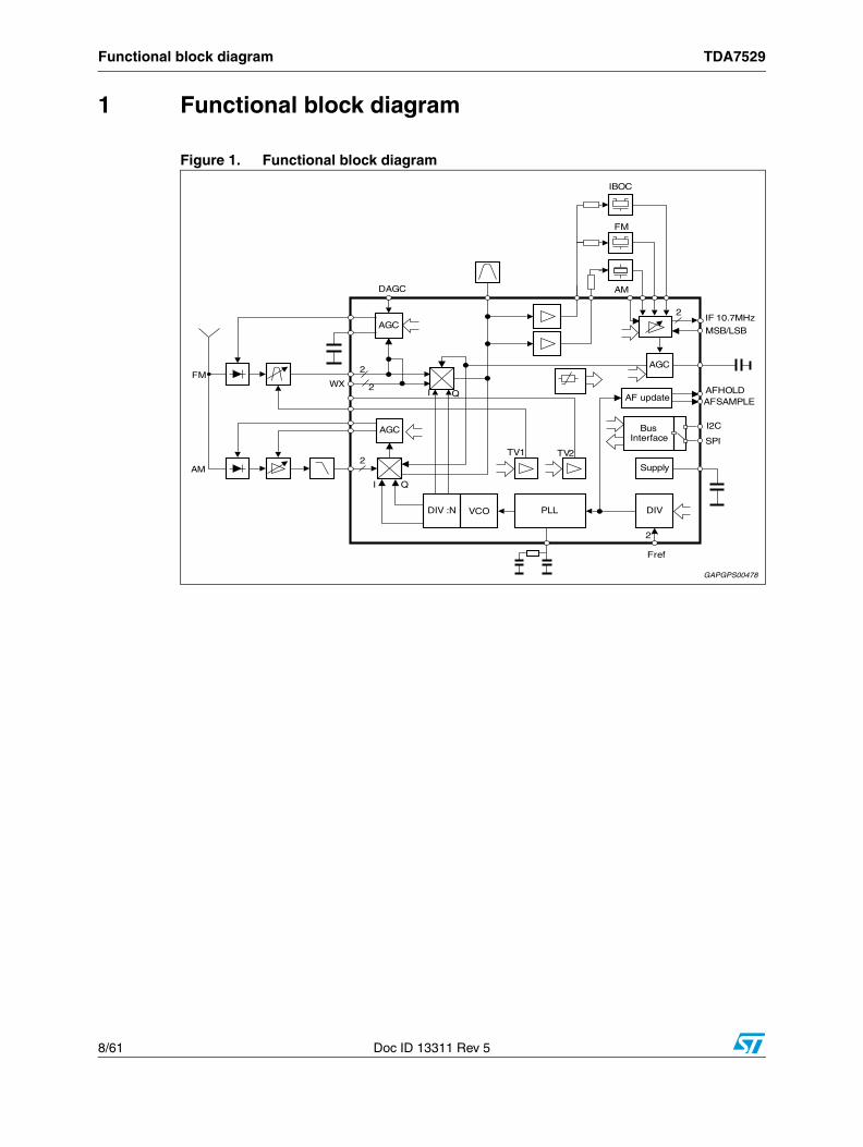
1 Functional block diagram
Figure 1. Functional block diagram
TDA7529 Pin description
Doc ID 13311 Rev 5 9/61
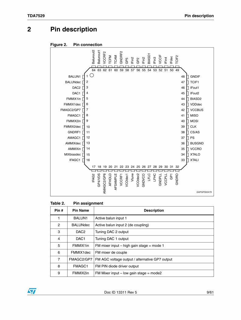
2 Pin description
Figure 2. Pin connection
Table 2. Pin assignment
Pin # Pin Name Description
1 BALUN1 Active balun input 1
2 BALUNdec Active balun input 2 (de coupling)
3 DAC2 Tuning DAC 2 output
4 DAC1 Tuning DAC 1 output
5 FMMIX1in FM mixer input – high gain stage = mode 1
6 FMMIX1dec FM mixer de couple
7 FMAGC2/GP7 FM AGC voltage output / alternative GP7 output
8 FMAGC1 FM PIN diode driver output
9 FMMIX2in FM Mixer input – low gain stage = mode2
Pin description TDA7529
10/61 Doc ID 13311 Rev 5
10 FMMIX2dec FM Mixer de couple
11 GNDRF1 GND RF1 section
12 AMAGC1 AMAGC PIN diode driver output
13 AMMIXdec AM mixer de couple
14 AMMIXin AM mixer input
15 MIXbiasdec Mixer bias de coupling
16 IFAGC1 IFAMP gain control via IFAGC - LSB
17 IFAGC2 IFAMP gain control via IFAGC - MSB
18 GP4/VDS GPIO 4 / VDS input
19AMAGC2 /
GP8AMAGC voltage output / alternative GP8 output
20 AFHOLD AF state machine hold output
21 AFSAMPLE AF state machine sample output
22 VCCRF1 Supply RF1 section
23 VCOdec1 BIAS de couple for VCO
24 Vtune VCO tuning voltage
25 VCOdec2 BIAS de couple for VCO
26 GNDVCO VCO Ground
27 LFLC Loop filter low current output
28 LFHC Loop filter high current output
29 GNDPLL PLL Ground
30 VCCPLL Supply PLL
31 GP1 GPIO 1
32 GNDRO Ground PLL digital part
33 XTALI Reference oscillator input
34 XTALO Reference oscillator output
35 VCCRO Supply PLL digital part
36 BUSGND BUSinterface Ground
37 PS Protocol Select
38 CS/AS Chip select / Address select
39 CLK SPI / I2C clodk
40 MOSI SPIdata input / I2C Data
41 MISO SPI Data Output
42 VCCBUS Supply of BUSinterface
43 VDDdec De couple of internal 3.3V (=3,3V + Vbe)
Table 2. Pin assignment (continued)
Pin # Pin Name Description
TDA7529 Pin description
Doc ID 13311 Rev 5 11/61
44 BIASD2 De coupling for Biasing
45 IFout2 Differential IF output 2
46 IFout1 Differential IF output 1
47 TCIF1 time constant IF AGC for AM
48 GNDIF ground IF section
49 TCIF2 time constant IF AGC for FM
50 IFdec De couple of IF amplifier
51 IFin4 IF input 4
52 VCCIF Supply IF section
53 IFin3 IF input 3
54 BIASD1 De coupling for Biasing
55 IFin2 IF input 2
56 GP2 GPIO 2
57 IFin1 IF input 1
58 GP5 GPIO 5
59 GNDRF2 GND RF2 section = active balun GND
60 TCAM AM AGC time constant
61 TCFM FM AGC time constant
62 VCCRF2 Supply voltage RF2 section
63 Balunout1 Active balun output 2 = FM output
64 Balunout2 Active balun output 1 = AM output
Table 2. Pin assignment (continued)
Pin # Pin Name Description
Function description TDA7529
12/61 Doc ID 13311 Rev 5
3 Function description
3.1 IMR mixer and active balun outputThe IMR mixer has two FM inputs (referred as mode 1 / mode 2) and one AM input selectable by software. The FM inputs differ by their gains, noise figures, IIP3 and maximum signal handling capability. The mode 1 FM input (with the higher gain, lower IIP3 and lower noise figure) is normally coupled with passive antenna input stages; the mode 2 FM input is normally used for input stages featuring an external preamplifier.
There are two single ended outputs of the IMR mixer: Balunout1 has a 4 dB higher gain than Balunout2. It is not recommended to use both outputs in parallel.
The Balun1 pin is the current mixer output over an internal resistor. The LC filter at Balun1 can be realized with a low cost SMD-coil (Q ~ 4).
3.2 FM RF-AGCThe FM AGC system is controlled by a peak detector, whose gain can be varied by the keyed AGC. The latter function is meant to be controlled by a D/A converter in the back-end part of the system.
The time constant of the FM RF-AGC is defined by an external capacitor connected to TCFM and programmable internal currents. The currents can be selected independently for AGC attack and decay. By this the ratio between the attack and the decay time can be programmed between 0.4 and 250.
The FM RF-AGC has two output pins to drive one PIN diode attenuator and the external preamplifier gain control.
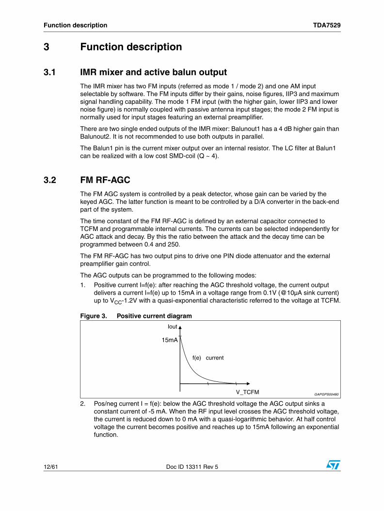
The AGC outputs can be programmed to the following modes:
1. Positive current I=f(e): after reaching the AGC threshold voltage, the current output delivers a current I=f(e) up to 15mA in a voltage range from 0.1V (@10µA sink current) up to VCC-1.2V with a quasi-exponential characteristic referred to the voltage at TCFM.
Figure 3. Positive current diagram
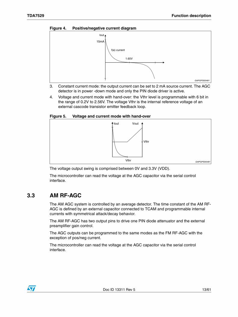
2. Pos/neg current I = f(e): below the AGC threshold voltage the AGC output sinks a constant current of -5 mA. When the RF input level crosses the AGC threshold voltage, the current is reduced down to 0 mA with a quasi-logarithmic behavior. At half control voltage the current becomes positive and reaches up to 15mA following an exponential function.
TDA7529 Function description
Doc ID 13311 Rev 5 13/61
Figure 4. Positive/negative current diagram
3. Constant current mode: the output current can be set to 2 mA source current. The AGC detector is in power -down mode and only the PIN diode driver is active.
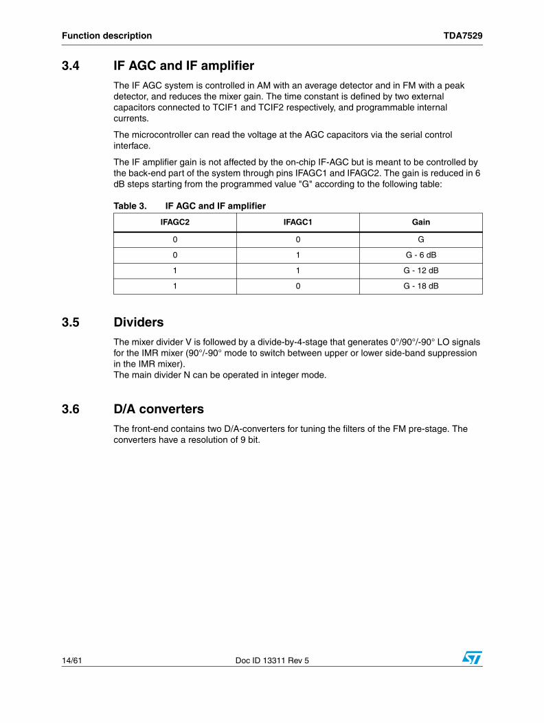
4. Voltage and current mode with hand-over: the Vthr level is programmable with 6 bit in the range of 0.2V to 2.56V. The voltage Vthr is the internal reference voltage of an external cascode transistor emitter feedback loop.
Figure 5. Voltage and current mode with hand-over
The voltage output swing is comprised between 0V and 3.3V (VDD).
The microcontroller can read the voltage at the AGC capacitor via the serial control interface.
3.3 AM RF-AGCThe AM AGC system is controlled by an average detector. The time constant of the AM RF-AGC is defined by an external capacitor connected to TCAM and programmable internal currents with symmetrical attack/decay behavior.
The AM RF-AGC has two output pins to drive one PIN diode attenuator and the external preamplifier gain control.
The AGC outputs can be programmed to the same modes as the FM RF-AGC with the exception of pos/neg current.
The microcontroller can read the voltage at the AGC capacitor via the serial control interface.
Function description TDA7529
14/61 Doc ID 13311 Rev 5
3.4 IF AGC and IF amplifierThe IF AGC system is controlled in AM with an average detector and in FM with a peak detector, and reduces the mixer gain. The time constant is defined by two external capacitors connected to TCIF1 and TCIF2 respectively, and programmable internal currents.
The microcontroller can read the voltage at the AGC capacitors via the serial control interface.
The IF amplifier gain is not affected by the on-chip IF-AGC but is meant to be controlled by the back-end part of the system through pins IFAGC1 and IFAGC2. The gain is reduced in 6 dB steps starting from the programmed value "G" according to the following table:
3.5 DividersThe mixer divider V is followed by a divide-by-4-stage that generates 0°/90°/-90° LO signals for the IMR mixer (90°/-90° mode to switch between upper or lower side-band suppression in the IMR mixer). The main divider N can be operated in integer mode.
3.6 D/A convertersThe front-end contains two D/A-converters for tuning the filters of the FM pre-stage. The converters have a resolution of 9 bit.
Table 3. IF AGC and IF amplifier
IFAGC2 IFAGC1 Gain
0 0 G
0 1 G - 6 dB
1 1 G - 12 dB
1 0 G - 18 dB
TDA7529 Function description
Doc ID 13311 Rev 5 15/61
3.7 VCOThe 3.7 GHz VCO has an internal switch that allows extending the oscillation frequency range. This is required by the fact that each of the two resulting VCO sub-bands (upper/lower) cannot individually cover the complete required frequency range versus temperature and process; for this reason a calibration procedure is needed to determine the process type (typical, slow, fast) and select the transition frequency between the two VCO sub-bands.
To run the procedure the VCO range 2 must be selected, the synthesized frequency needs to be set to 4GHz; then if Vtuning > 2.6V then the process is 'slow', if Vtuning < 1.7V then is 'fast' and otherwise is 'typical'. The switching frequency as a function of the process is reported in the following table:
3.8 FREFThe reference frequency for the PLL can be derived by a XTAL directly connected to the device or by means of an LVDS signal. In the latter case an external matching resistor must be used to obtain the desired input signal level.
3.9 A/D converterThe front-end contains a 6 bit SAR A/D-converter for sensing several analog values of the tuner. The following analog sources can be switched to the ADC input by software command:
● FM RF AGC capacitor voltage
● AM RF AGC capacitor voltage
● IF AGC capacitor voltage (automatically connected to the FM or AM IF AGC filtering capacitor)
● PLL tuning voltage
● Temperature sensor
● GPIO 1 voltage
● GPIO 2 voltage
● ADC reference generated from VCC.
The ADC can be clocked by an integrated RC-oscillator, in which case the oscillation frequency is programmable, or by the PLL reference frequency.
Table 4. Switching frequency as a function of the process
Slow Typ. Fast
3.635 GHz 3.72 GHz 3.794 GHz
Function description TDA7529
16/61 Doc ID 13311 Rev 5
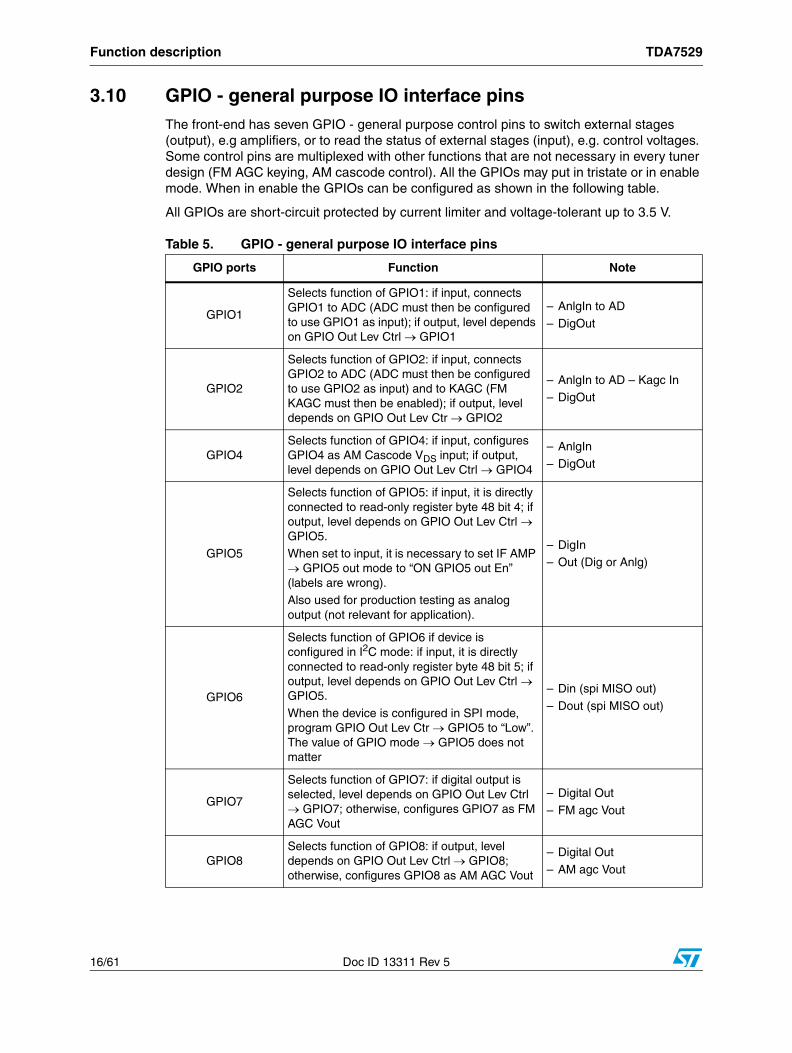
3.10 GPIO - general purpose IO interface pinsThe front-end has seven GPIO - general purpose control pins to switch external stages (output), e.g amplifiers, or to read the status of external stages (input), e.g. control voltages. Some control pins are multiplexed with other functions that are not necessary in every tuner design (FM AGC keying, AM cascode control). All the GPIOs may put in tristate or in enable mode. When in enable the GPIOs can be configured as shown in the following table.
All GPIOs are short-circuit protected by current limiter and voltage-tolerant up to 3.5 V.
Table 5. GPIO - general purpose IO interface pins
GPIO ports Function Note
GPIO1
Selects function of GPIO1: if input, connects GPIO1 to ADC (ADC must then be configured to use GPIO1 as input); if output, level depends on GPIO Out Lev Ctrl GPIO1
– AnlgIn to AD
– DigOut
GPIO2
Selects function of GPIO2: if input, connects GPIO2 to ADC (ADC must then be configured to use GPIO2 as input) and to KAGC (FM KAGC must then be enabled); if output, level depends on GPIO Out Lev Ctr GPIO2
– AnlgIn to AD – Kagc In
– DigOut
GPIO4Selects function of GPIO4: if input, configures GPIO4 as AM Cascode VDS input; if output, level depends on GPIO Out Lev Ctrl GPIO4
– AnlgIn
– DigOut
GPIO5
Selects function of GPIO5: if input, it is directly connected to read-only register byte 48 bit 4; if output, level depends on GPIO Out Lev Ctrl GPIO5.
When set to input, it is necessary to set IF AMP GPIO5 out mode to “ON GPIO5 out En” (labels are wrong).Also used for production testing as analog output (not relevant for application).
– DigIn– Out (Dig or Anlg)
GPIO6
Selects function of GPIO6 if device is configured in I2C mode: if input, it is directly connected to read-only register byte 48 bit 5; if output, level depends on GPIO Out Lev Ctrl GPIO5.
When the device is configured in SPI mode, program GPIO Out Lev Ctr GPIO5 to “Low”. The value of GPIO mode GPIO5 does not matter
– Din (spi MISO out)
– Dout (spi MISO out)
GPIO7
Selects function of GPIO7: if digital output is selected, level depends on GPIO Out Lev Ctrl GPIO7; otherwise, configures GPIO7 as FM AGC Vout
– Digital Out
– FM agc Vout
GPIO8Selects function of GPIO8: if output, level depends on GPIO Out Lev Ctrl GPIO8; otherwise, configures GPIO8 as AM AGC Vout
– Digital Out
– AM agc Vout
TDA7529 Function description
Doc ID 13311 Rev 5 17/61
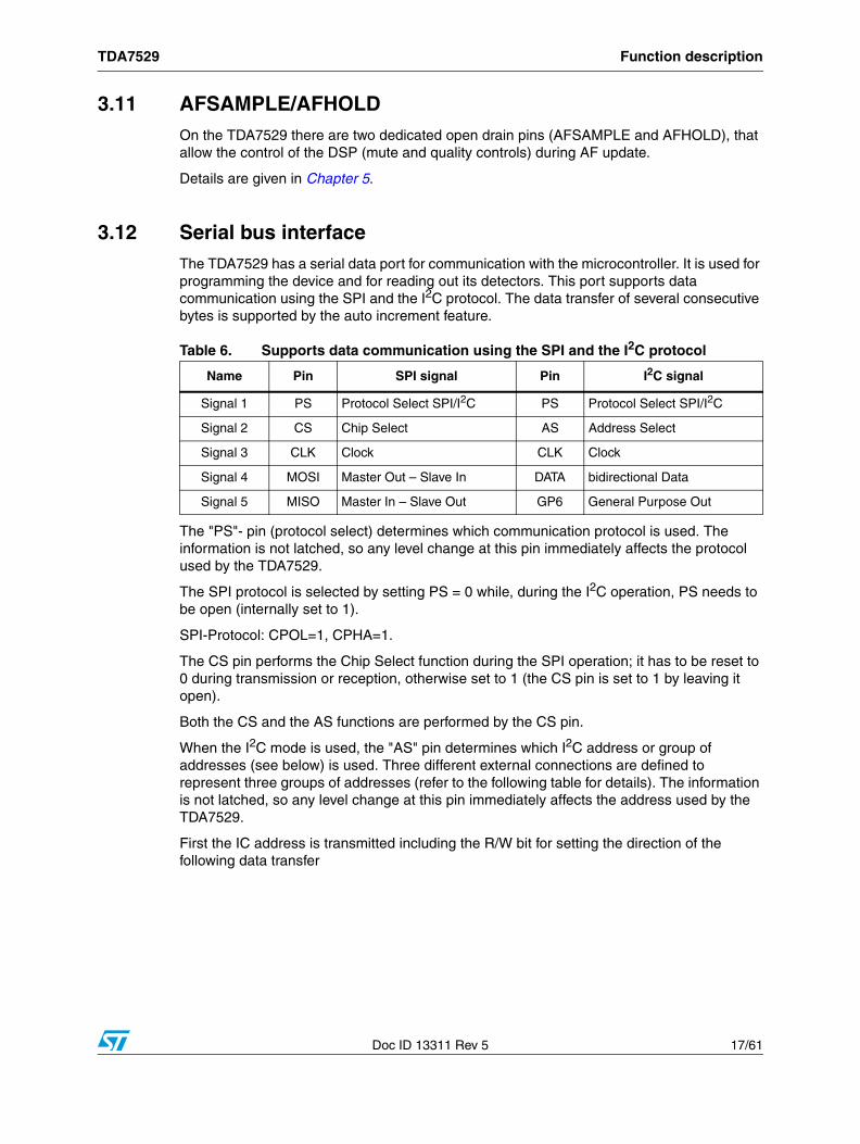
3.11 AFSAMPLE/AFHOLDOn the TDA7529 there are two dedicated open drain pins (AFSAMPLE and AFHOLD), that allow the control of the DSP (mute and quality controls) during AF update.
Details are given in Chapter 5.
3.12 Serial bus interfaceThe TDA7529 has a serial data port for communication with the microcontroller. It is used for programming the device and for reading out its detectors. This port supports data communication using the SPI and the I2C protocol. The data transfer of several consecutive bytes is supported by the auto increment feature.
The "PS"- pin (protocol select) determines which communication protocol is used. The information is not latched, so any level change at this pin immediately affects the protocol used by the TDA7529.
The SPI protocol is selected by setting PS = 0 while, during the I2C operation, PS needs to be open (internally set to 1).
SPI-Protocol: CPOL=1, CPHA=1.
The CS pin performs the Chip Select function during the SPI operation; it has to be reset to 0 during transmission or reception, otherwise set to 1 (the CS pin is set to 1 by leaving it open).
Both the CS and the AS functions are performed by the CS pin.
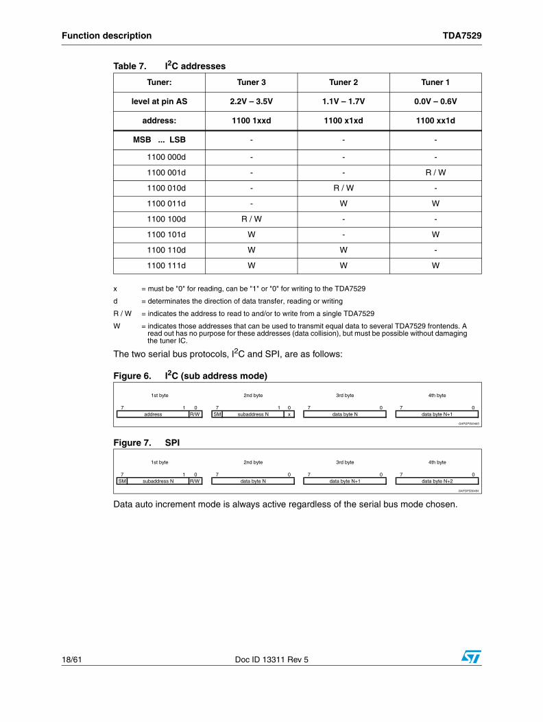
When the I2C mode is used, the "AS" pin determines which I2C address or group of addresses (see below) is used. Three different external connections are defined to represent three groups of addresses (refer to the following table for details). The information is not latched, so any level change at this pin immediately affects the address used by the TDA7529.
First the IC address is transmitted including the R/W bit for setting the direction of the following data transfer
Table 6. Supports data communication using the SPI and the I2C protocol
Name Pin SPI signal Pin I2C signal
Signal 1 PS Protocol Select SPI/I2C PS Protocol Select SPI/I2C
Signal 2 CS Chip Select AS Address Select
Signal 3 CLK Clock CLK Clock
Signal 4 MOSI Master Out – Slave In DATA bidirectional Data
Signal 5 MISO Master In – Slave Out GP6 General Purpose Out
Function description TDA7529
18/61 Doc ID 13311 Rev 5
x = must be "0" for reading, can be "1" or "0" for writing to the TDA7529
d = determinates the direction of data transfer, reading or writing
R / W = indicates the address to read to and/or to write from a single TDA7529
W = indicates those addresses that can be used to transmit equal data to several TDA7529 frontends. A read out has no purpose for these addresses (data collision), but must be possible without damaging the tuner IC.
The two serial bus protocols, I2C and SPI, are as follows:
Figure 6. I2C (sub address mode)
Figure 7. SPI
Data auto increment mode is always active regardless of the serial bus mode chosen.
Table 7. I2C addresses
Tuner: Tuner 3 Tuner 2 Tuner 1
level at pin AS 2.2V – 3.5V 1.1V – 1.7V 0.0V – 0.6V
address: 1100 1xxd 1100 x1xd 1100 xx1d
MSB ... LSB - - -
1100 000d - - -
1100 001d - - R / W
1100 010d - R / W -
1100 011d - W W
1100 100d R / W - -
1100 101d W - W
1100 110d W W -
1100 111d W W W
TDA7529 Electrical specifications
Doc ID 13311 Rev 5 19/61
4 Electrical specifications
Electrical parameters are guaranteed if Fref = 100kHz, with frequency stability of +/- 20ppm max.
4.1 Absolute maximum ratings
4.2 Thermal data
4.3 General key parameters
Table 8. Absolute maximum ratings
Symbol Parameter Test condition Min Typ Max Units
VCC Abs. supply voltage - - - 5.5 V
Tamb Ambient temperature range - -40 - 105 °C
Tstg Storage temperature - -55 - 150 °C
Tj Junction temperature - - - 150 °C
Table 9. Thermal data
Symbol Parameter Test condition, comments Min Typ Max Units
Rthj-ambThermal resistance junction to ambient
2s2p std Jedec board with thermal via underneath the component (36 board via: diameter = 0.5mm / pitch = 1.5mm), max 30% missing soldering
- - 33 °C/W
Table 10. General key parameters
Symbol Parameter Test Condition, Comments Min Typ Max Units
VCC 5V supply voltage - 4.7 5 5.35 V
ICC Supply current @ 5V - - 145 175 mA
ICC_pwdSupply current @ 5V in power down mode
- - 9 14 mA
Tamb Ambient temperature range - -40 - 105 °C
Electrical specifications TDA7529
20/61 Doc ID 13311 Rev 5
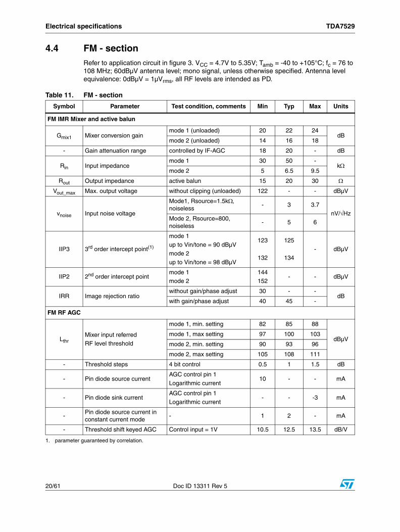
4.4 FM - sectionRefer to application circuit in figure 3. VCC = 4.7V to 5.35V; Tamb = -40 to +105°C; fc = 76 to 108 MHz; 60dBµV antenna level; mono signal, unless otherwise specified. Antenna level equivalence: 0dBµV = 1µVrms, all RF levels are intended as PD.
Table 11. FM - section
Symbol Parameter Test condition, comments Min Typ Max Units
FM IMR Mixer and active balun
Gmix1 Mixer conversion gainmode 1 (unloaded) 20 22 24
dBmode 2 (unloaded) 14 16 18
- Gain attenuation range controlled by IF-AGC 18 20 - dB
Rin Input impedancemode 1 30 50 -
kmode 2 5 6.5 9.5
Rout Output impedance active balun 15 20 30
Vout_max Max. output voltage without clipping (unloaded) 122 - - dBµV
vnoise Input noise voltage
Mode1, Rsource=1.5k, noiseless
- 3 3.7nV/Hz
Mode 2, Rsource=800, noiseless
- 5 6
IIP3 3rd order intercept point(1)
mode 1 up to Vin/tone = 90 dBµV
mode 2
up to Vin/tone = 98 dBµV
123
132
125
134- dBµV
IIP2 2nd order intercept pointmode 1mode 2
144152
- - dBµV
IRR Image rejection ratiowithout gain/phase adjust 30 - -
dBwith gain/phase adjust 40 45 -
FM RF AGC
LthrMixer input referred RF level threshold
mode 1, min. setting 82 85 88
dBµVmode 1, max setting 97 100 103
mode 2, min. setting 90 93 96
mode 2, max setting 105 108 111
- Threshold steps 4 bit control 0.5 1 1.5 dB
- Pin diode source current AGC control pin 1
Logarithmic current10 - - mA
- Pin diode sink currentAGC control pin 1
Logarithmic current- - -3 mA
-Pin diode source current in constant current mode
- 1 2 - mA
- Threshold shift keyed AGC Control input = 1V 10.5 12.5 13.5 dB/V
1. parameter guaranteed by correlation.
TDA7529 Electrical specifications
Doc ID 13311 Rev 5 21/61
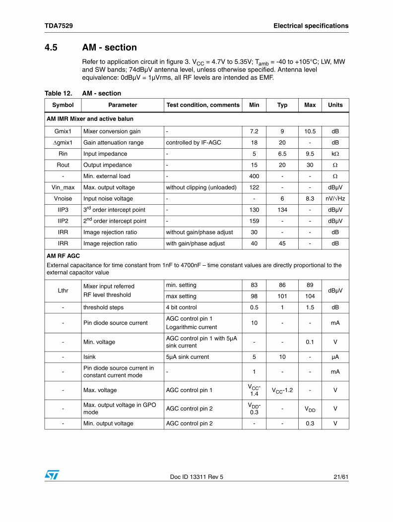
4.5 AM - sectionRefer to application circuit in figure 3. VCC = 4.7V to 5.35V; Tamb = -40 to +105°C; LW, MW and SW bands; 74dBµV antenna level, unless otherwise specified. Antenna level equivalence: 0dBµV = 1µVrms, all RF levels are intended as EMF.
Table 12. AM - section
Symbol Parameter Test condition, comments Min Typ Max Units
AM IMR Mixer and active balun
Gmix1 Mixer conversion gain - 7.2 9 10.5 dB
gmix1 Gain attenuation range controlled by IF-AGC 18 20 - dB
Rin Input impedance - 5 6.5 9.5 k
Rout Output impedance - 15 20 30
- Min. external load - 400 - -
Vin_max Max. output voltage without clipping (unloaded) 122 - - dBµV
Vnoise Input noise voltage - - 6 8.3 nV/Hz
IIP3 3rd order intercept point - 130 134 - dBµV
IIP2 2nd order intercept point - 159 - - dBµV
IRR Image rejection ratio without gain/phase adjust 30 - - dB
IRR Image rejection ratio with gain/phase adjust 40 45 - dB
AM RF AGC
External capacitance for time constant from 1nF to 4700nF – time constant values are directly proportional to the external capacitor value
LthrMixer input referred
RF level threshold
min. setting 83 86 89dBµV
max setting 98 101 104
- threshold steps 4 bit control 0.5 1 1.5 dB
- Pin diode source current AGC control pin 1Logarithmic current
10 - - mA
- Min. voltageAGC control pin 1 with 5µA sink current
- - 0.1 V
- Isink 5µA sink current 5 10 - µA
-Pin diode source current in constant current mode
- 1 - - mA
- Max. voltage AGC control pin 1VCC-1.4
VCC-1.2 - V
-Max. output voltage in GPO mode
AGC control pin 2VDD-0.3
- VDD V
- Min. output voltage AGC control pin 2 - - 0.3 V
Electrical specifications TDA7529
22/61 Doc ID 13311 Rev 5
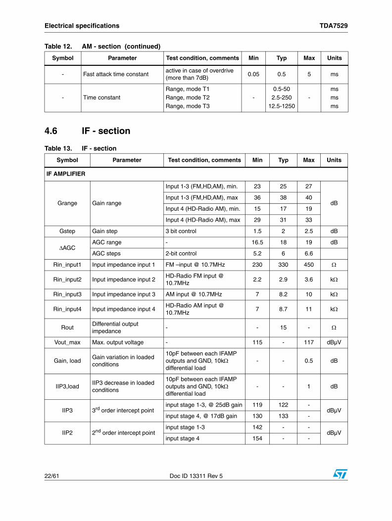
4.6 IF - section
- Fast attack time constantactive in case of overdrive (more than 7dB)
0.05 0.5 5 ms
- Time constant Range, mode T1Range, mode T2
Range, mode T3
-0.5-502.5-250
12.5-1250
-msms
ms
Table 12. AM - section (continued)
Symbol Parameter Test condition, comments Min Typ Max Units
Table 13. IF - section
Symbol Parameter Test condition, comments Min Typ Max Units
IF AMPLIFIER
Grange Gain range
Input 1-3 (FM,HD,AM), min. 23 25 27
dBInput 1-3 (FM,HD,AM), max 36 38 40
Input 4 (HD-Radio AM), min. 15 17 19
Input 4 (HD-Radio AM), max 29 31 33
Gstep Gain step 3 bit control 1.5 2 2.5 dB
AGCAGC range - 16.5 18 19 dB
AGC steps 2-bit control 5.2 6 6.6
Rin_input1 Input impedance input 1 FM –input @ 10.7MHz 230 330 450
Rin_input2 Input impedance input 2HD-Radio FM input @ 10.7MHz
2.2 2.9 3.6 k
Rin_input3 Input impedance input 3 AM input @ 10.7MHz 7 8.2 10 k
Rin_input4 Input impedance input 4HD-Radio AM input @ 10.7MHz
7 8.7 11 k
RoutDifferential output impedance
- - 15 -
Vout_max Max. output voltage - 115 - 117 dBµV
Gain, loadGain variation in loaded conditions
10pF between each IFAMP outputs and GND, 10k differential load
- - 0.5 dB
IIP3,loadIIP3 decrease in loaded conditions
10pF between each IFAMP outputs and GND, 10k differential load
- - 1 dB
IIP3 3rd order intercept point input stage 1-3, @ 25dB gain 119 122 -
dBµVinput stage 4, @ 17dB gain 130 133 -
IIP2 2nd order intercept pointinput stage 1-3 142 - -
dBµVinput stage 4 154 - -
TDA7529 Electrical specifications
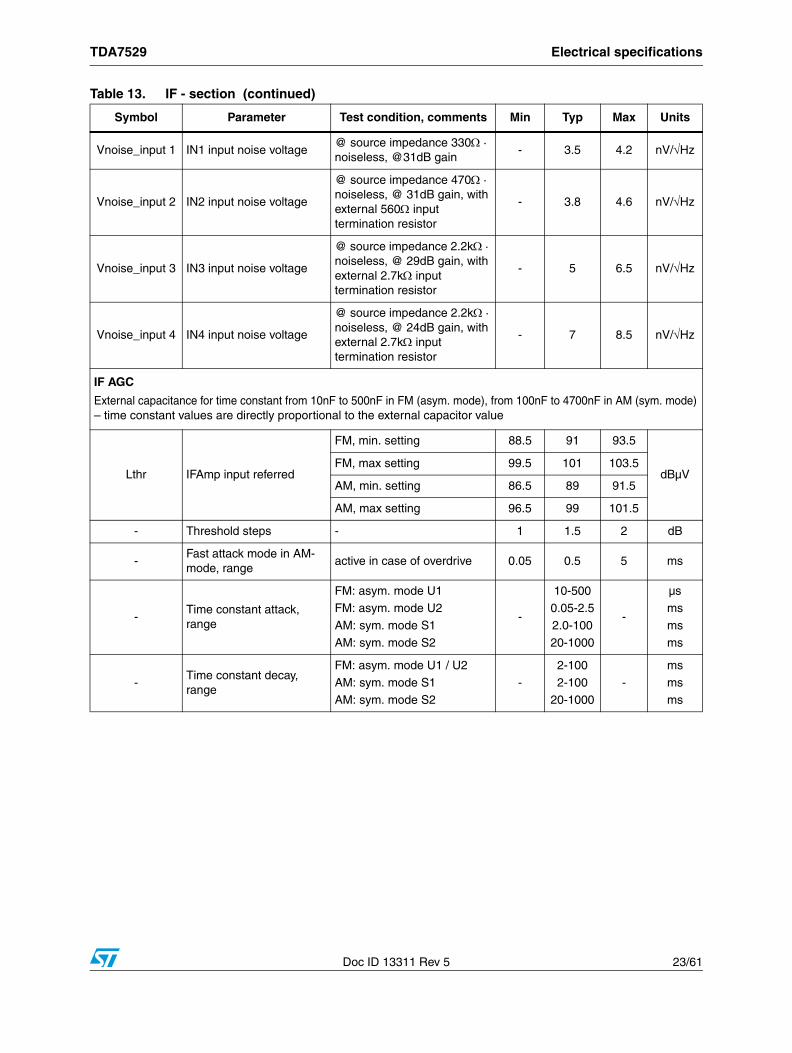
Doc ID 13311 Rev 5 23/61
Vnoise_input 1 IN1 input noise voltage @ source impedance 330·noiseless, @31dB gain
- 3.5 4.2 nV/Hz
Vnoise_input 2 IN2 input noise voltage
@ source impedance 470· noiseless, @ 31dB gain, with external 560 input termination resistor
- 3.8 4.6 nV/Hz
Vnoise_input 3 IN3 input noise voltage
@ source impedance 2.2k· noiseless, @ 29dB gain, with external 2.7k input termination resistor
- 5 6.5 nV/Hz
Vnoise_input 4 IN4 input noise voltage
@ source impedance 2.2k·noiseless, @ 24dB gain, with external 2.7k input termination resistor
- 7 8.5 nV/Hz
IF AGC
External capacitance for time constant from 10nF to 500nF in FM (asym. mode), from 100nF to 4700nF in AM (sym. mode)– time constant values are directly proportional to the external capacitor value
Lthr IFAmp input referred
FM, min. setting 88.5 91 93.5
dBµVFM, max setting 99.5 101 103.5
AM, min. setting 86.5 89 91.5
AM, max setting 96.5 99 101.5
- Threshold steps - 1 1.5 2 dB
-Fast attack mode in AM-mode, range
active in case of overdrive 0.05 0.5 5 ms
-Time constant attack, range
FM: asym. mode U1FM: asym. mode U2
AM: sym. mode S1
AM: sym. mode S2
-
10-5000.05-2.5
2.0-100
20-1000
-
µsms
ms
ms
-Time constant decay, range
FM: asym. mode U1 / U2
AM: sym. mode S1 AM: sym. mode S2
-
2-100
2-10020-1000
-
ms
msms
Table 13. IF - section (continued)
Symbol Parameter Test condition, comments Min Typ Max Units
Electrical specifications TDA7529
24/61 Doc ID 13311 Rev 5
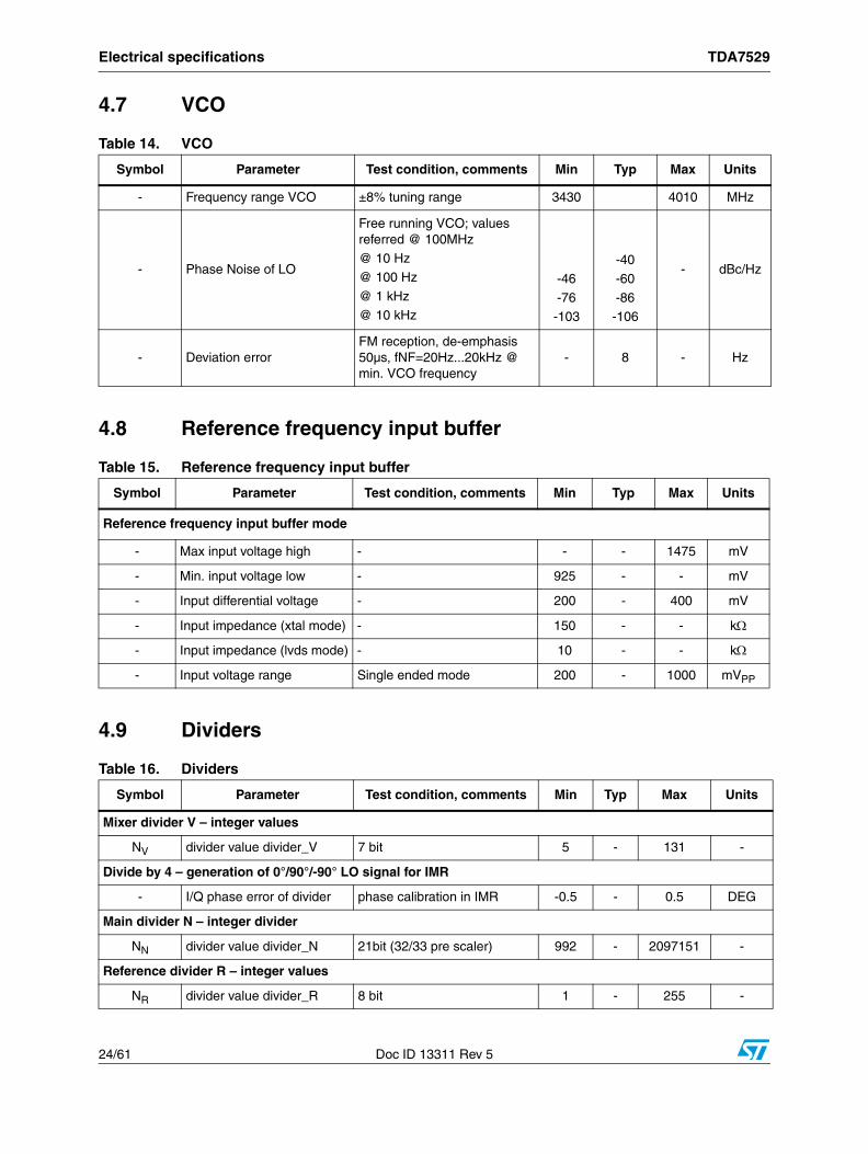
4.7 VCO
4.8 Reference frequency input buffer
4.9 Dividers
Table 14. VCO
Symbol Parameter Test condition, comments Min Typ Max Units
- Frequency range VCO ±8% tuning range 3430 4010 MHz
- Phase Noise of LO
Free running VCO; values referred @ 100MHz
@ 10 Hz@ 100 Hz
@ 1 kHz
@ 10 kHz
-46
-76-103
-40
-60
-86-106
- dBc/Hz
- Deviation errorFM reception, de-emphasis 50µs, fNF=20Hz...20kHz @ min. VCO frequency
- 8 - Hz
Table 15. Reference frequency input buffer
Symbol Parameter Test condition, comments Min Typ Max Units
Reference frequency input buffer mode
- Max input voltage high - - - 1475 mV
- Min. input voltage low - 925 - - mV
- Input differential voltage - 200 - 400 mV
- Input impedance (xtal mode) - 150 - - k
- Input impedance (lvds mode) - 10 - - k
- Input voltage range Single ended mode 200 - 1000 mVPP
Table 16. Dividers
Symbol Parameter Test condition, comments Min Typ Max Units
Mixer divider V – integer values
NV divider value divider_V 7 bit 5 - 131 -
Divide by 4 – generation of 0°/90°/-90° LO signal for IMR
- I/Q phase error of divider phase calibration in IMR -0.5 - 0.5 DEG
Main divider N – integer divider
NN divider value divider_N 21bit (32/33 pre scaler) 992 - 2097151 -
Reference divider R – integer values
NR divider value divider_R 8 bit 1 - 255 -
TDA7529 Electrical specifications
Doc ID 13311 Rev 5 25/61
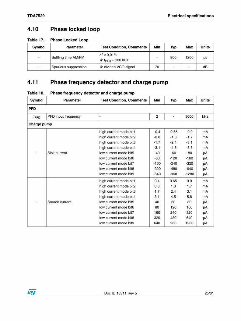
4.10 Phase locked loop
4.11 Phase frequency detector and charge pump
Table 17. Phase Locked Loop
Symbol Parameter Test Condition, Comments Min Typ Max Units
- Settling time AM/FMf < 0,01%@ fPFD = 100 kHz
- 800 1200 µs
- Spurious suppression @ divided VCO signal 70 - - dB
Table 18. Phase frequency detector and charge pump
Symbol Parameter Test Condition, Comments Min Typ Max Units
PFD
fPFD PFD input frequency - 2 - 3000 kHz
Charge pump
- Sink current
high current mode bit1
high current mode bit2
high current mode bit3high current mode bit4
low current mode bit5
low current mode bit6low current mode bit7
low current mode bit8
low current mode bit9
-0.4
-0.8
-1.7-3.1
-40
-80-160
-320
-640
-0.65
-1.3
-2.4-4.5
-60
-120-240
-480
-960
-0.9
-1.7
-3.1-5.8
-80
-160-320
-640
-1280
mA
mA
mAmA
µA
µAµA
µA
µA
- Source current
high current mode bit1
high current mode bit2high current mode bit3
high current mode bit4
low current mode bit5low current mode bit6
low current mode bit7
low current mode bit8
low current mode bit9
0.4
0.81.7
3.1
4080
160
320
640
0.65
1.32.4
4.5
60120
240
480
960
0.9
1.73.1
5.8
80160
320
640
1280
mA
mAmA
mA
µAµA
µA
µA
µA
Electrical specifications TDA7529
26/61 Doc ID 13311 Rev 5
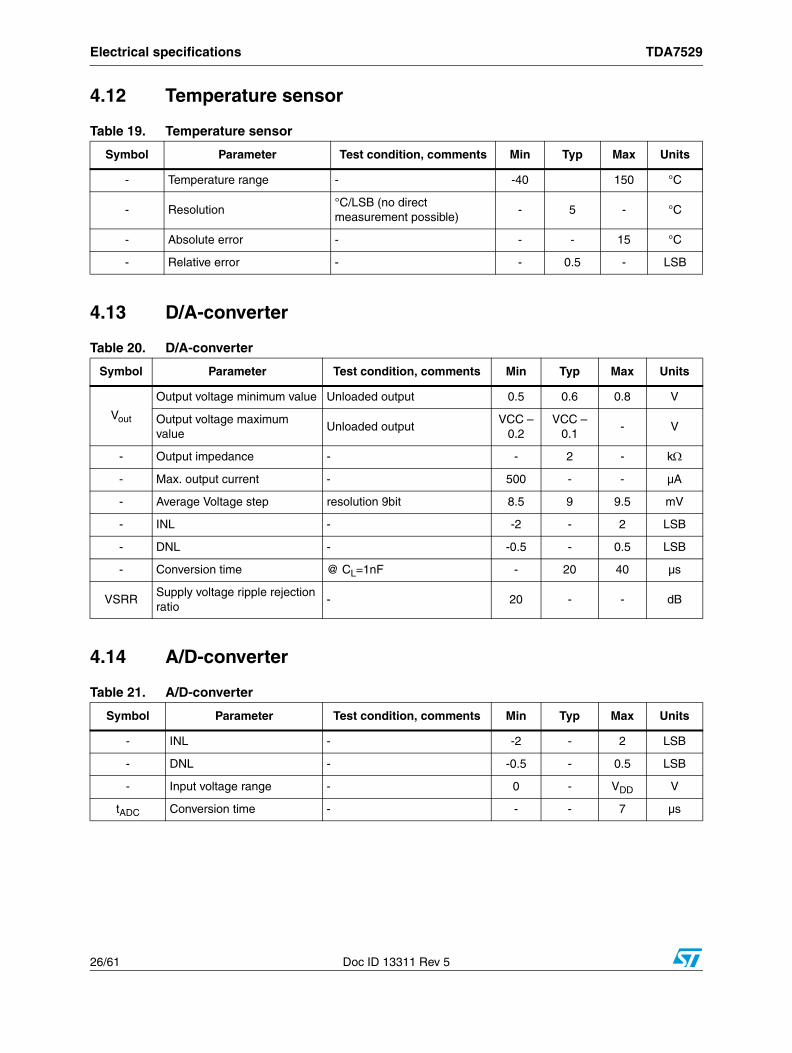
4.12 Temperature sensor
4.13 D/A-converter
4.14 A/D-converter
Table 19. Temperature sensor
Symbol Parameter Test condition, comments Min Typ Max Units
- Temperature range - -40 150 °C
- Resolution°C/LSB (no direct measurement possible)
- 5 - °C
- Absolute error - - - 15 °C
- Relative error - - 0.5 - LSB
Table 20. D/A-converter
Symbol Parameter Test condition, comments Min Typ Max Units
Vout
Output voltage minimum value Unloaded output 0.5 0.6 0.8 V
Output voltage maximum value
Unloaded outputVCC –
0.2VCC –
0.1- V
- Output impedance - - 2 - k
- Max. output current - 500 - - µA
- Average Voltage step resolution 9bit 8.5 9 9.5 mV
- INL - -2 - 2 LSB
- DNL - -0.5 - 0.5 LSB
- Conversion time @ CL=1nF - 20 40 µs
VSRRSupply voltage ripple rejection ratio
- 20 - - dB
Table 21. A/D-converter
Symbol Parameter Test condition, comments Min Typ Max Units
- INL - -2 - 2 LSB
- DNL - -0.5 - 0.5 LSB
- Input voltage range - 0 - VDD V
tADC Conversion time - - - 7 µs
TDA7529 Electrical specifications
Doc ID 13311 Rev 5 27/61
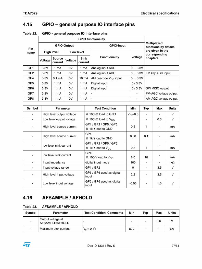
4.15 GPIO – general purpose IO interface pins
4.16 AFSAMPLE / AFHOLD
Table 22. GPIO - general purpose IO interface pins
Pinname
GPIO functionalityMultiplexed functionality details are given in the corresponding chapters
GPIO-Output GPIO-Input
High level Low level
Functionality VoltageVoltage
Source current
VoltageSink
current
GP1 3.3V 1 mA 0V 1 mA Analog input ADC 0 ... 3.3V
GP2 3.3V 1 mA 0V 1 mA Analog input ADC 0 ... 3.3V FM key AGC input
GP4 3.3V 0.1 mA 0V 10 mA AM cascode VDS input 0 ... 3.3V
GP5 3.3V 1 mA 0V 1 mA Digital Input 0 / 3.3V
GP6 3.3V 1 mA 0V 1 mA Digital Input 0 / 3.3V SPI MISO output
GP7 3.3V 1 mA 0V 1 mA - - FM-AGC voltage output
GP8 3.3V 1 mA 0V 1 mA - - AM-AGC voltage output
Symbol Parameter Test Condition Min Typ Max Units
- High level output voltage @ 100k load to GND VDD-0.3 - - V
- Low level output voltage @ 100k load to VDD - - 0.3 V
- High level source currentGP1 / GP2 / GP5 / GP6:@ 1k load to GND
0.5 1 - mA
- High level source currentGP4
@ 1k load to GND0.08 0.1 - mA
- low level sink currentGP1 / GP2 / GP5 / GP6:
@ 1k load to VDD 0.8 1-
mA
- low level sink currentGP4:@ 100 load to VDD 8.0 10
-mA
- Input impedance digital input mode 100 - - k
- Input voltage range GP1 / GP2 0 - 3.5 V
- High level input voltageGP5 / GP6 used as digital input
2.2 - 3.5 V
- Low level input voltageGP5 / GP6 used as digital input
-0.05 - 1.0 V
Table 23. AFSAMPLE / AFHOLD
Symbol Parameter Test Condition, Comments Min Typ Max Units
-Output voltage at AFSAMPLE/AFHOLD
- - - 3.6 V
- Maximum sink current Vo = 0.4V 800 - - A
Electrical specifications TDA7529
28/61 Doc ID 13311 Rev 5
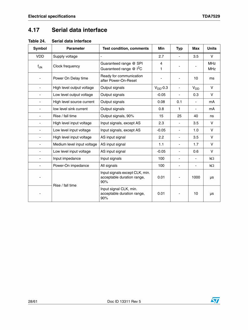
4.17 Serial data interface
Table 24. Serial data interface
Symbol Parameter Test condition, comments Min Typ Max Units
VDD Supply voltage - 2.7 - 3.5 V
fclk Clock frequencyGuaranteed range @ SPI
Guaranteed range @ I2C
4
1- -
MHz
MHz
- Power On Delay timeReady for communication after Power-On-Reset
- - 10 ms
- High level output voltage Output signals VDD-0.3 - VDD V
- Low level output voltage Output signals -0.05 - 0.3 V
- High level source current Output signals 0.08 0.1 - mA
- low level sink current Output signals 0.8 1 - mA
- Rise / fall time Output signals, 90% 15 25 40 ns
- High level input voltage Input signals, except AS 2.3 - 3.5 V
- Low level input voltage Input signals, except AS -0.05 - 1.0 V
- High level input voltage AS input signal 2.2 - 3.5 V
- Medium level input voltage AS input signal 1.1 - 1.7 V
- Low level input voltage AS input signal -0.05 - 0.6 V
- Input impedance Input signals 100 - - k
- Power-On impedance All signals 100 - - k
-
Rise / fall time
Input signals except CLK, min. acceptable duration range, 90%
0.01 - 1000 µs
-Input signal CLK, min. acceptable duration range, 90%
0.01 - 10 µs
TDA7529 Tuning state machine
Doc ID 13311 Rev 5 29/61
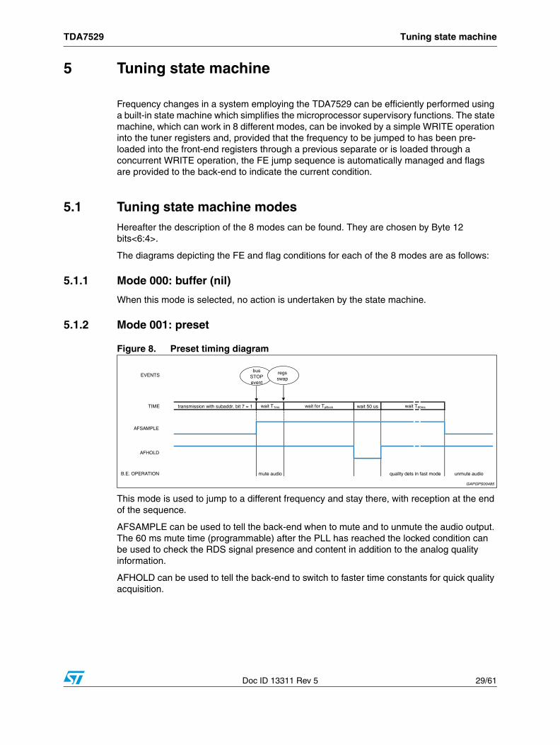
5 Tuning state machine
Frequency changes in a system employing the TDA7529 can be efficiently performed using a built-in state machine which simplifies the microprocessor supervisory functions. The state machine, which can work in 8 different modes, can be invoked by a simple WRITE operation into the tuner registers and, provided that the frequency to be jumped to has been pre-loaded into the front-end registers through a previous separate or is loaded through a concurrent WRITE operation, the FE jump sequence is automatically managed and flags are provided to the back-end to indicate the current condition.
5.1 Tuning state machine modesHereafter the description of the 8 modes can be found. They are chosen by Byte 12 bits<6:4>.
The diagrams depicting the FE and flag conditions for each of the 8 modes are as follows:
5.1.1 Mode 000: buffer (nil)
When this mode is selected, no action is undertaken by the state machine.
5.1.2 Mode 001: preset
Figure 8. Preset timing diagram
This mode is used to jump to a different frequency and stay there, with reception at the end of the sequence.
AFSAMPLE can be used to tell the back-end when to mute and to unmute the audio output. The 60 ms mute time (programmable) after the PLL has reached the locked condition can be used to check the RDS signal presence and content in addition to the analog quality information.
AFHOLD can be used to tell the back-end to switch to faster time constants for quick quality acquisition.
Tuning state machine TDA7529
30/61 Doc ID 13311 Rev 5
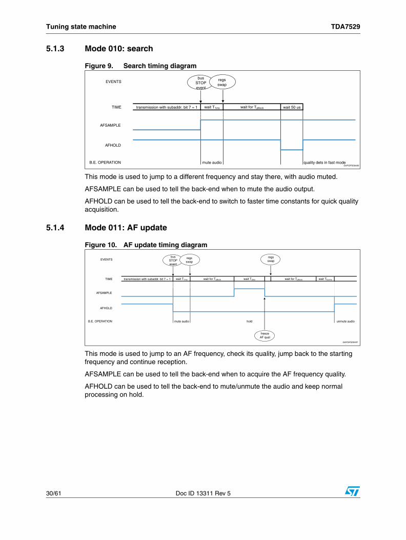
5.1.3 Mode 010: search
Figure 9. Search timing diagram
This mode is used to jump to a different frequency and stay there, with audio muted.
AFSAMPLE can be used to tell the back-end when to mute the audio output.
AFHOLD can be used to tell the back-end to switch to faster time constants for quick quality acquisition.
5.1.4 Mode 011: AF update
Figure 10. AF update timing diagram
This mode is used to jump to an AF frequency, check its quality, jump back to the starting frequency and continue reception.
AFSAMPLE can be used to tell the back-end when to acquire the AF frequency quality.
AFHOLD can be used to tell the back-end to mute/unmute the audio and keep normal processing on hold.
TDA7529 Tuning state machine
Doc ID 13311 Rev 5 31/61
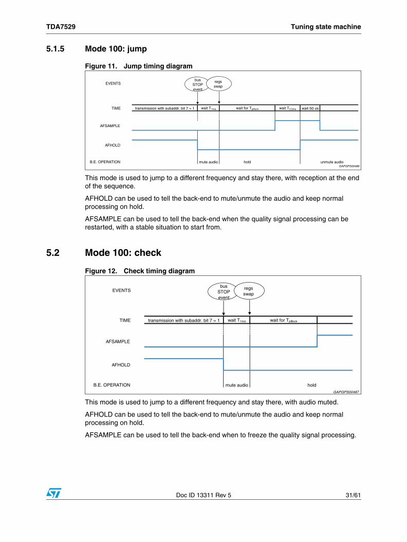
5.1.5 Mode 100: jump
Figure 11. Jump timing diagram
This mode is used to jump to a different frequency and stay there, with reception at the end of the sequence.
AFHOLD can be used to tell the back-end to mute/unmute the audio and keep normal processing on hold.
AFSAMPLE can be used to tell the back-end when the quality signal processing can be restarted, with a stable situation to start from.
5.2 Mode 100: check
Figure 12. Check timing diagram
This mode is used to jump to a different frequency and stay there, with audio muted.
AFHOLD can be used to tell the back-end to mute/unmute the audio and keep normal processing on hold.
AFSAMPLE can be used to tell the back-end when to freeze the quality signal processing.
Tuning state machine TDA7529
32/61 Doc ID 13311 Rev 5
5.3 Mode 110: load
Figure 13. Load timing diagram
The content of the buffer and control registers is swapped. No transition occurs on the AFHOLD and AFSAMPLE lines.
5.4 Mode 111: end
Figure 14. End timing diagram
This mode is used to end sequences that terminate with muted audio, after the decision on whether to stay to that frequency or jump to a different one has been taken.
AFHOLD can be used to tell the back-end to unmute the audio.
AFSAMPLE can be used to tell the back-end to restore normal quality signal processing.
Most of the wait times of the algorithm can actually be programmed.
The following table summarizes the minimum, maximum and default values of the programmable wait times. The indicated values are valid only for the advised configuration where the phase detector reference frequency is 100 kHz.
TDA7529 Tuning state machine
Doc ID 13311 Rev 5 33/61
5.5 Register SWAPSome of these modes contain one or two register "swap" operation(s). The changes within the register structure during a swap operation depend on the operating mode of the chip.
If the chip is programmed in the "buffer/control" mode (chosen by setting byte 12 bit 7 = 1), which is necessary to take advantage of the tuning state machine, it is suggested that the microprocessor write data only in the normal register bank (bytes from 16 to 31), because the state machine itself takes care of exchanging the content of the normal register bank with that of the shadow bank (bytes from 32 to 47) during a swap. The normal registers are intended to be written to by the radio microprocessor, whereas the registers that actually control the device circuits are the shadow ones.
In any case it is suggested that the bits 5 and 4 of byte 0, that define which control bank is actually used to drive the device circuits, should not be touched after setting them to 0 after reset because they are automatically updated by the tuning state machine.
Table 25. Values of the programmable wait times
PARAMETER NAME REGISTER VALUE TIME
Tplllock Byte 15 bits<7:3>
min. 00000 20 us
default 00110 1 ms
maximum 11111 5 ms
T0.5ms Byte 30 bits<7:2>
min. 000000 70 us
default 000101 0.5 ms
maximum 111111 5 ms
T1ms Byte 20 bits<7:2>
min. 000000 10 us
default 001100 1 ms
maximum 111111 5 ms
T2ms Byte 29 bits<7:2>
min. 000000 50 us
default 011000 2 ms
maximum 111111 5 ms
T60ms Byte 04 bits<7:3>
min. 00000 1 ms
default 10111 60 ms
maximum 11111 80 ms
Tuning state machine TDA7529
34/61 Doc ID 13311 Rev 5
5.6 State machine startThe tuning state machine is activated only at the end of the transmission if bit 7 of the subaddress is 1. The activation sequence, therefore, is to be done in the following way.
Figure 15. Buffer/control serial bus sequence
TD
A7529
Reg
isters descrip
tion
Doc ID
13311 Rev 5
35/61
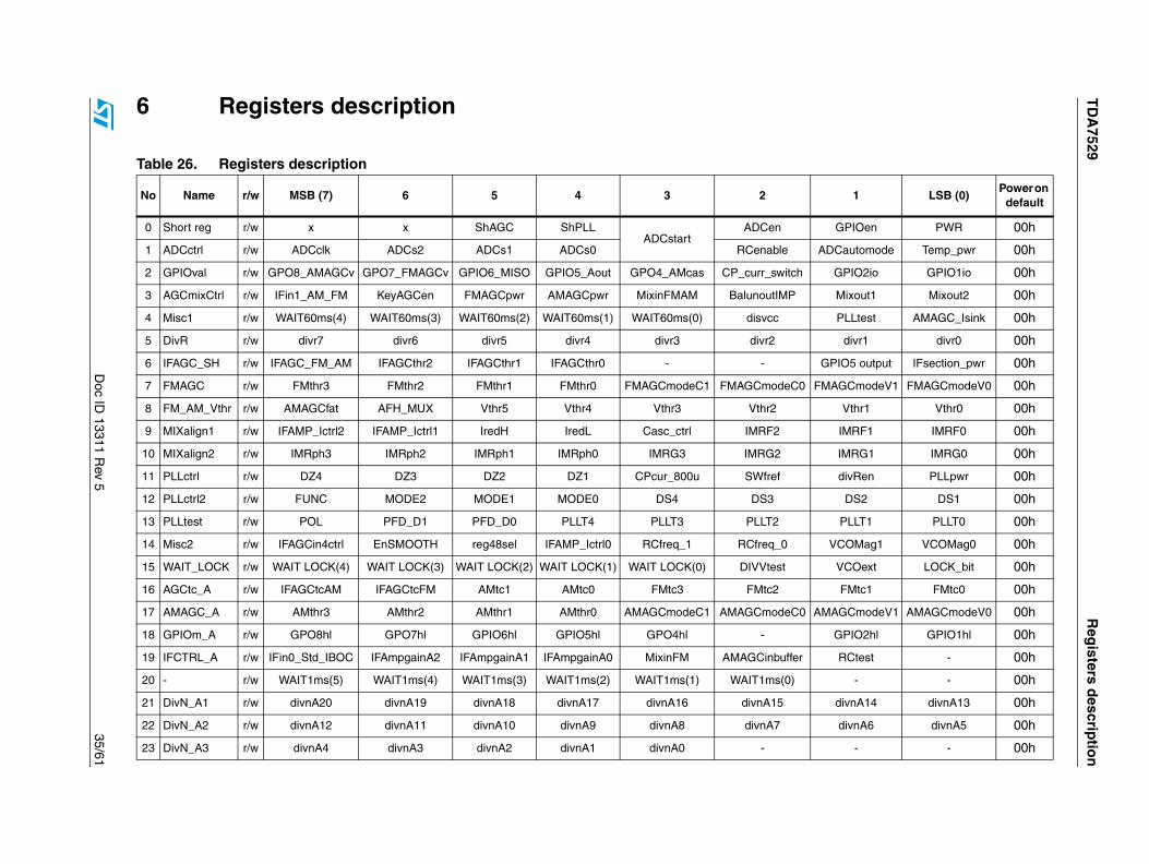
6 Registers description
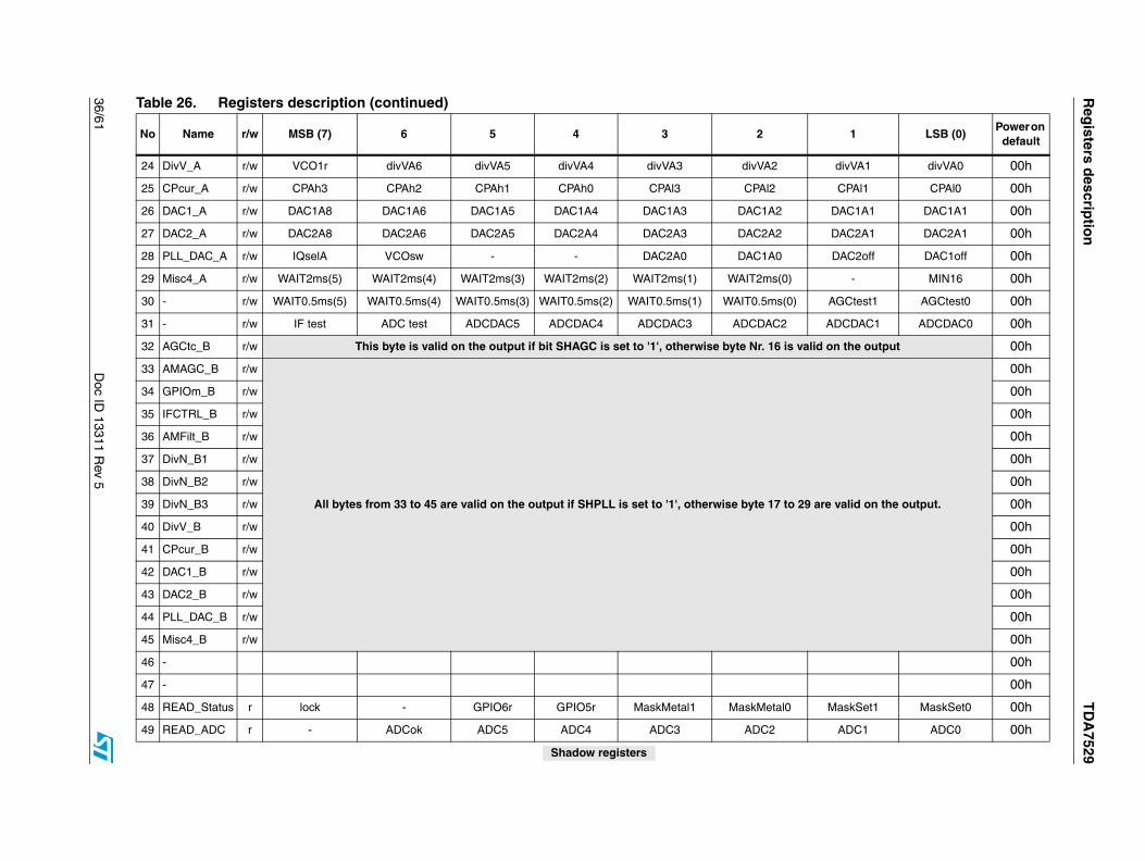
Table 26. Registers description
No Name r/w MSB (7) 6 5 4 3 2 1 LSB (0)Power on
default
0 Short reg r/w x x ShAGC ShPLLADCstart
ADCen GPIOen PWR 00h
1 ADCctrl r/w ADCclk ADCs2 ADCs1 ADCs0 RCenable ADCautomode Temp_pwr 00h
2 GPIOval r/w GPO8_AMAGCv GPO7_FMAGCv GPIO6_MISO GPIO5_Aout GPO4_AMcas CP_curr_switch GPIO2io GPIO1io 00h
3 AGCmixCtrl r/w IFin1_AM_FM KeyAGCen FMAGCpwr AMAGCpwr MixinFMAM BalunoutIMP Mixout1 Mixout2 00h
4 Misc1 r/w WAIT60ms(4) WAIT60ms(3) WAIT60ms(2) WAIT60ms(1) WAIT60ms(0) disvcc PLLtest AMAGC_Isink 00h
5 DivR r/w divr7 divr6 divr5 divr4 divr3 divr2 divr1 divr0 00h
6 IFAGC_SH r/w IFAGC_FM_AM IFAGCthr2 IFAGCthr1 IFAGCthr0 - - GPIO5 output IFsection_pwr 00h
7 FMAGC r/w FMthr3 FMthr2 FMthr1 FMthr0 FMAGCmodeC1 FMAGCmodeC0 FMAGCmodeV1 FMAGCmodeV0 00h
8 FM_AM_Vthr r/w AMAGCfat AFH_MUX Vthr5 Vthr4 Vthr3 Vthr2 Vthr1 Vthr0 00h
9 MIXalign1 r/w IFAMP_Ictrl2 IFAMP_Ictrl1 IredH IredL Casc_ctrl IMRF2 IMRF1 IMRF0 00h
10 MIXalign2 r/w IMRph3 IMRph2 IMRph1 IMRph0 IMRG3 IMRG2 IMRG1 IMRG0 00h
11 PLLctrl r/w DZ4 DZ3 DZ2 DZ1 CPcur_800u SWfref divRen PLLpwr 00h
12 PLLctrl2 r/w FUNC MODE2 MODE1 MODE0 DS4 DS3 DS2 DS1 00h
13 PLLtest r/w POL PFD_D1 PFD_D0 PLLT4 PLLT3 PLLT2 PLLT1 PLLT0 00h
14 Misc2 r/w IFAGCin4ctrl EnSMOOTH reg48sel IFAMP_Ictrl0 RCfreq_1 RCfreq_0 VCOMag1 VCOMag0 00h
15 WAIT_LOCK r/w WAIT LOCK(4) WAIT LOCK(3) WAIT LOCK(2) WAIT LOCK(1) WAIT LOCK(0) DIVVtest VCOext LOCK_bit 00h
16 AGCtc_A r/w IFAGCtcAM IFAGCtcFM AMtc1 AMtc0 FMtc3 FMtc2 FMtc1 FMtc0 00h
17 AMAGC_A r/w AMthr3 AMthr2 AMthr1 AMthr0 AMAGCmodeC1 AMAGCmodeC0 AMAGCmodeV1 AMAGCmodeV0 00h
18 GPIOm_A r/w GPO8hl GPO7hl GPIO6hl GPIO5hl GPO4hl - GPIO2hl GPIO1hl 00h
19 IFCTRL_A r/w IFin0_Std_IBOC IFAmpgainA2 IFAmpgainA1 IFAmpgainA0 MixinFM AMAGCinbuffer RCtest - 00h
20 - r/w WAIT1ms(5) WAIT1ms(4) WAIT1ms(3) WAIT1ms(2) WAIT1ms(1) WAIT1ms(0) - - 00h
21 DivN_A1 r/w divnA20 divnA19 divnA18 divnA17 divnA16 divnA15 divnA14 divnA13 00h
22 DivN_A2 r/w divnA12 divnA11 divnA10 divnA9 divnA8 divnA7 divnA6 divnA5 00h
23 DivN_A3 r/w divnA4 divnA3 divnA2 divnA1 divnA0 - - - 00h
Reg
isters descrip
tion
TD
A7529
36/61D
oc ID 13311 R
ev 5
24 DivV_A r/w VCO1r divVA6 divVA5 divVA4 divVA3 divVA2 divVA1 divVA0 00h
25 CPcur_A r/w CPAh3 CPAh2 CPAh1 CPAh0 CPAl3 CPAl2 CPAl1 CPAl0 00h
26 DAC1_A r/w DAC1A8 DAC1A6 DAC1A5 DAC1A4 DAC1A3 DAC1A2 DAC1A1 DAC1A1 00h
27 DAC2_A r/w DAC2A8 DAC2A6 DAC2A5 DAC2A4 DAC2A3 DAC2A2 DAC2A1 DAC2A1 00h
28 PLL_DAC_A r/w IQselA VCOsw - - DAC2A0 DAC1A0 DAC2off DAC1off 00h
29 Misc4_A r/w WAIT2ms(5) WAIT2ms(4) WAIT2ms(3) WAIT2ms(2) WAIT2ms(1) WAIT2ms(0) - MIN16 00h
30 - r/w WAIT0.5ms(5) WAIT0.5ms(4) WAIT0.5ms(3) WAIT0.5ms(2) WAIT0.5ms(1) WAIT0.5ms(0) AGCtest1 AGCtest0 00h
31 - r/w IF test ADC test ADCDAC5 ADCDAC4 ADCDAC3 ADCDAC2 ADCDAC1 ADCDAC0 00h
32 AGCtc_B r/w This byte is valid on the output if bit SHAGC is set to '1', otherwise byte Nr. 16 is valid on the output 00h
33 AMAGC_B r/w
All bytes from 33 to 45 are valid on the output if SHPLL is set to '1', otherwise byte 17 to 29 are valid on the output.
00h
34 GPIOm_B r/w 00h
35 IFCTRL_B r/w 00h
36 AMFilt_B r/w 00h
37 DivN_B1 r/w 00h
38 DivN_B2 r/w 00h
39 DivN_B3 r/w 00h
40 DivV_B r/w 00h
41 CPcur_B r/w 00h
42 DAC1_B r/w 00h
43 DAC2_B r/w 00h
44 PLL_DAC_B r/w 00h
45 Misc4_B r/w 00h
46 - 00h
47 - 00h
48 READ_Status r lock - GPIO6r GPIO5r MaskMetal1 MaskMetal0 MaskSet1 MaskSet0 00h
49 READ_ADC r - ADCok ADC5 ADC4 ADC3 ADC2 ADC1 ADC0 00h
Table 26. Registers description (continued)
No Name r/w MSB (7) 6 5 4 3 2 1 LSB (0)Power on
default
Shadow registers
TDA7529 Registers description
Doc ID 13311 Rev 5 37/61
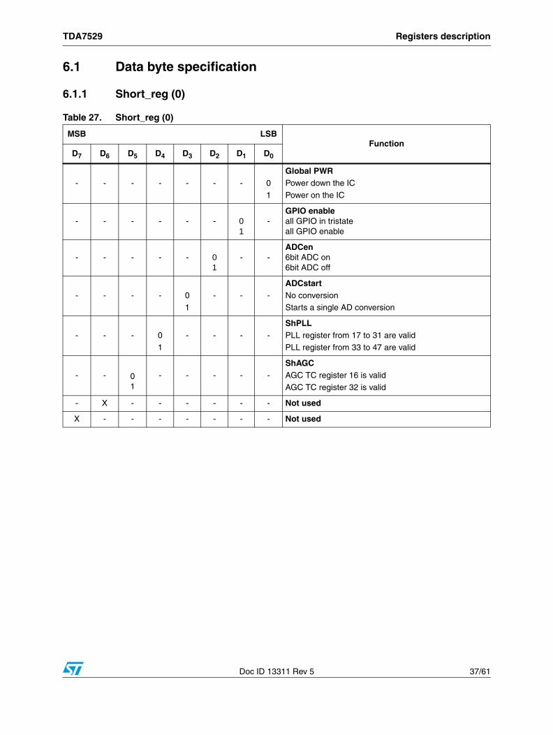
6.1 Data byte specification
6.1.1 Short_reg (0)
Table 27. Short_reg (0)
MSB LSBFunction
D7 D6 D5 D4 D3 D2 D1 D0
- - - - - - - 0
1
Global PWRPower down the IC
Power on the IC
- - - - - - 01
-GPIO enableall GPIO in tristateall GPIO enable
- - - - - 01
- -ADCen6bit ADC on6bit ADC off
- - - - 01
- - -
ADCstartNo conversionStarts a single AD conversion
- - - 0
1
- - - -ShPLLPLL register from 17 to 31 are valid
PLL register from 33 to 47 are valid
- - 01
- - - - -
ShAGCAGC TC register 16 is valid
AGC TC register 32 is valid
- X - - - - - - Not used
X - - - - - - - Not used
Registers description TDA7529
38/61 Doc ID 13311 Rev 5
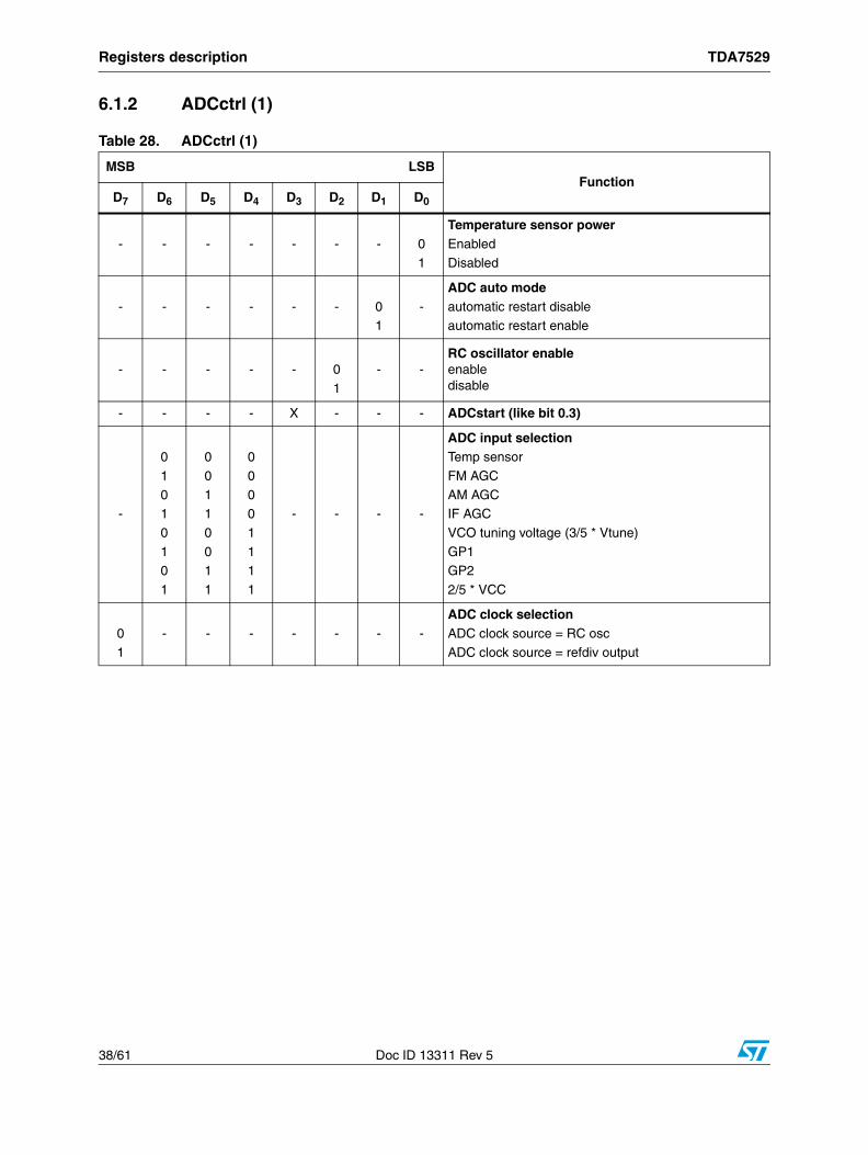
6.1.2 ADCctrl (1)
Table 28. ADCctrl (1)
MSB LSBFunction
D7 D6 D5 D4 D3 D2 D1 D0
- - - - - - - 0
1
Temperature sensor powerEnabled
Disabled
- - - - - - 01
-
ADC auto modeautomatic restart disable automatic restart enable
- - - - - 0
1
- -RC oscillator enableenabledisable
- - - - X - - - ADCstart (like bit 0.3)
-
0
1
01
0
10
1
0
0
11
0
01
1
0
0
00
1
11
1
- - - -
ADC input selectionTemp sensor
FM AGC
AM AGCIF AGC
VCO tuning voltage (3/5 * Vtune)
GP1GP2
2/5 * VCC
0
1
- - - - - - -
ADC clock selectionADC clock source = RC osc
ADC clock source = refdiv output
TDA7529 Registers description
Doc ID 13311 Rev 5 39/61
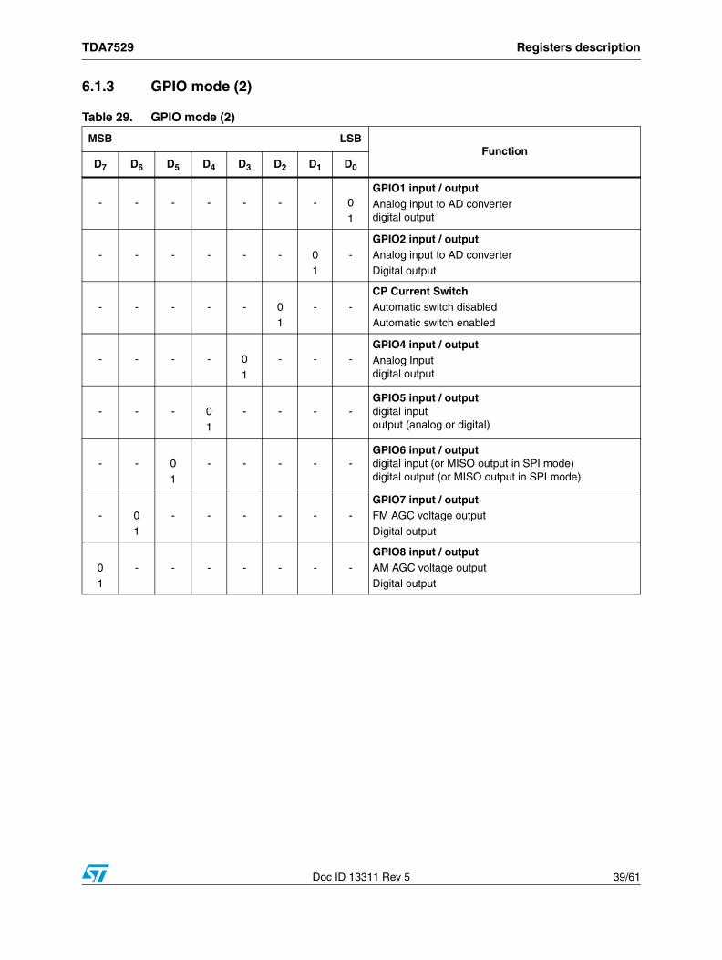
6.1.3 GPIO mode (2)
Table 29. GPIO mode (2)
MSB LSBFunction
D7 D6 D5 D4 D3 D2 D1 D0
- - - - - - - 0
1
GPIO1 input / outputAnalog input to AD converterdigital output
- - - - - - 01
-
GPIO2 input / outputAnalog input to AD converterDigital output
- - - - - 0
1
- -CP Current SwitchAutomatic switch disabled
Automatic switch enabled
- - - - 0
1
- - -GPIO4 input / outputAnalog Inputdigital output
- - - 01
- - - -GPIO5 input / outputdigital inputoutput (analog or digital)
- - 0
1
- - - - -GPIO6 input / outputdigital input (or MISO output in SPI mode)digital output (or MISO output in SPI mode)
- 0
1
- - - - - -
GPIO7 input / outputFM AGC voltage output
Digital output
01
- - - - - - -
GPIO8 input / outputAM AGC voltage outputDigital output
Registers description TDA7529
40/61 Doc ID 13311 Rev 5
6.1.4 AGC and mixer control (3)
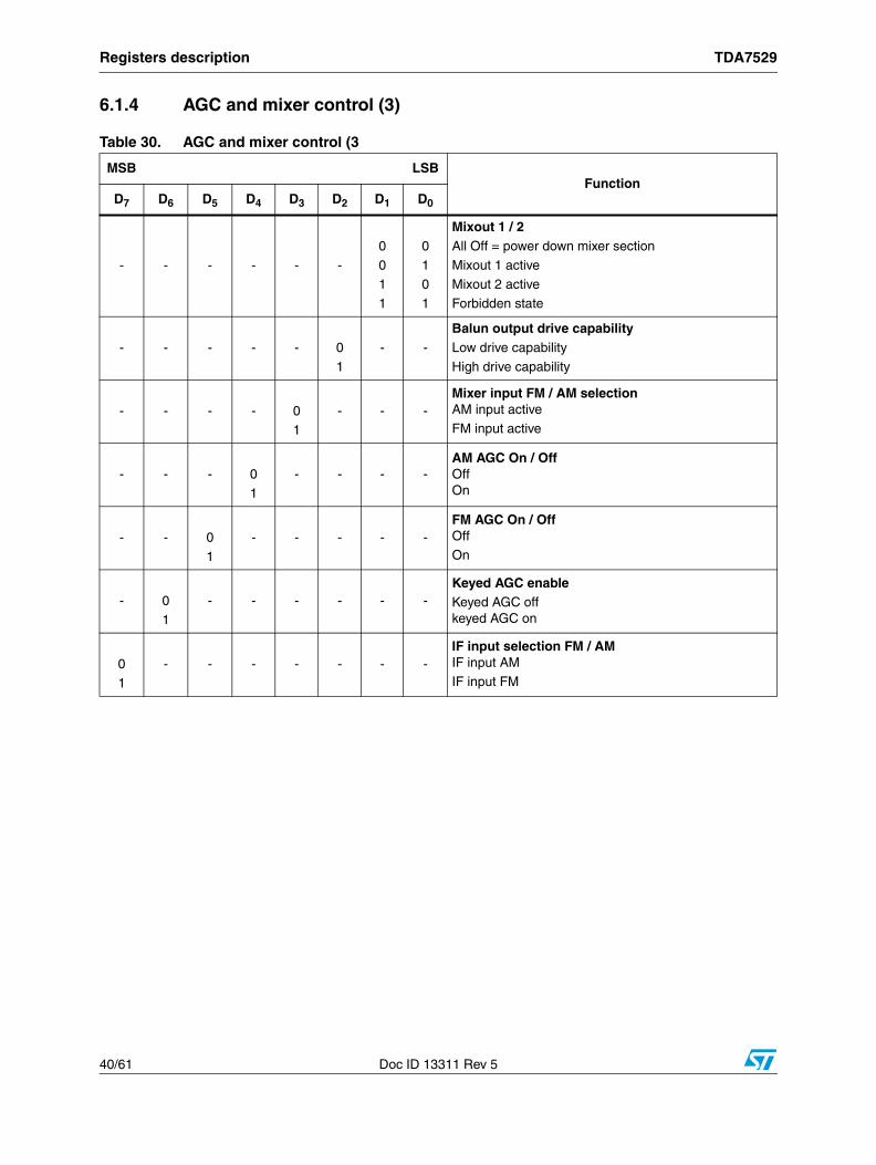
Table 30. AGC and mixer control (3
MSB LSBFunction
D7 D6 D5 D4 D3 D2 D1 D0
- - - - - -
0
01
1
0
10
1
Mixout 1 / 2All Off = power down mixer section
Mixout 1 activeMixout 2 active
Forbidden state
- - - - - 0
1
- -
Balun output drive capabilityLow drive capability
High drive capability
- - - - 01
- - -Mixer input FM / AM selectionAM input active
FM input active
- - - 0
1
- - - -AM AGC On / OffOffOn
- - 0
1
- - - - -FM AGC On / OffOff
On
- 01
- - - - - -Keyed AGC enableKeyed AGC offkeyed AGC on
0
1
- - - - - - -IF input selection FM / AMIF input AM IF input FM
TDA7529 Registers description
Doc ID 13311 Rev 5 41/61
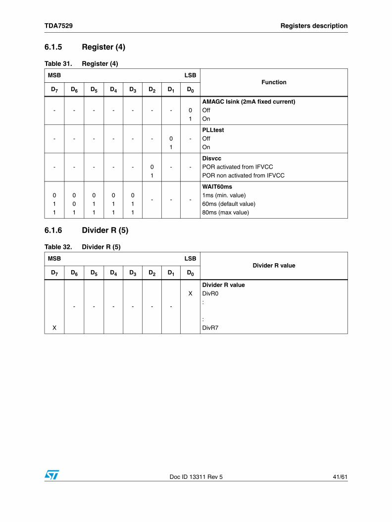
6.1.5 Register (4)
6.1.6 Divider R (5)
Table 31. Register (4)
MSB LSBFunction
D7 D6 D5 D4 D3 D2 D1 D0
- - - - - - - 0
1
AMAGC Isink (2mA fixed current)Off
On
- - - - - - 01
-
PLLtestOffOn
- - - - - 0
1
- -DisvccPOR activated from IFVCC
POR non activated from IFVCC
0
11
0
01
0
11
0
11
0
11
- - -
WAIT60ms1ms (min. value)
60ms (default value)80ms (max value)
Table 32. Divider R (5)
MSB LSBDivider R value
D7 D6 D5 D4 D3 D2 D1 D0
X
- - - - - -
XDivider R valueDivR0
:
:
DivR7
Registers description TDA7529
42/61 Doc ID 13311 Rev 5
6.1.7 IF AGC control (6)
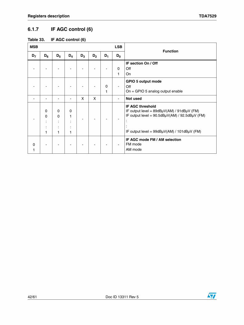
Table 33. IF AGC control (6)
MSB LSBFunction
D7 D6 D5 D4 D3 D2 D1 D0
- - - - - - - 0
1
IF section On / OffOff
On
- - - - - - 01
-GPIO 5 output modeOffOn = GPIO 5 analog output enable
- - - - X X - Not used
-
00
:
:1
00
:
:1
01
:
:1
- - - -
IF AGC thresholdIF output level = 89dBµV(AM) / 91dBµV (FM)IF output level = 90.5dBµV(AM) / 92.5dBµV (FM)
::
IF output level = 99dBµV(AM) / 101dBµV (FM)
0
1
- - - - - - -IF AGC mode FM / AM selectionFM modeAM mode
TDA7529 Registers description
Doc ID 13311 Rev 5 43/61
6.1.8 FM AGC (7)
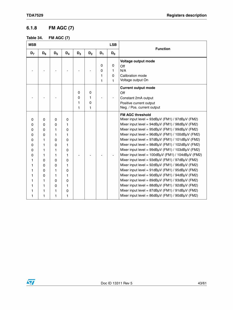
Table 34. FM AGC (7)
MSB LSBFunction
D7 D6 D5 D4 D3 D2 D1 D0
- - - - - -
0
01
1
0
10
1
Voltage output modeOffN/ACalibration modeVoltage output On
- - -
0
01
1
0
10
1
- -
Current output modeOffConstant 2mA output
Positive current outputNeg. / Pos. current output
0
00
0
00
0
01
1
11
1
11
1
0
00
0
11
1
10
0
00
1
11
1
0
01
1
00
1
10
0
11
0
01
1
0
10
1
01
0
10
1
01
0
10
1
- - - -
FM AGC thresholdMixer input level = 93dBµV (FM1) / 97dBµV (FM2)
Mixer input level = 94dBµV (FM1) / 98dBµV (FM2)
Mixer input level = 95dBµV (FM1) / 99dBµV (FM2)Mixer input level = 96dBµV (FM1) / 100dBµV (FM2)
Mixer input level = 97dBµV (FM1) / 101dBµV (FM2)
Mixer input level = 98dBµV (FM1) / 102dBµV (FM2)Mixer input level = 99dBµV (FM1) / 103dBµV (FM2)
Mixer input level = 100dBµV (FM1) / 104dBµV (FM2)
Mixer input level = 93dBµV (FM1) / 97dBµV (FM2)Mixer input level = 92dBµV (FM1) / 96dBµV (FM2)
Mixer input level = 91dBµV (FM1) / 95dBµV (FM2)
Mixer input level = 90dBµV (FM1) / 94dBµV (FM2)Mixer input level = 89dBµV (FM1) / 93dBµV (FM2)
Mixer input level = 88dBµV (FM1) / 92dBµV (FM2)
Mixer input level = 87dBµV (FM1) / 91dBµV (FM2)Mixer input level = 86dBµV (FM1) / 90dBµV (FM2)
Registers description TDA7529
44/61 Doc ID 13311 Rev 5
6.1.9 AGC voltage threshold (8)
6.1.10 Mixer alignment 1 (9)
Table 35. AGC voltage threshold (8)
MSB LSBFunction
D7 D6 D5 D4 D3 D2 D1 D0
- -
0
0:
:
11
0
0:
:
11
0
0:
:
11
0
0:
:
11
0
0:
:
11
01
:
:0
1
Transfer voltage from voltage out to current out200mV237.5mV:
:
2.5625V2.6V
0
1
- - - - - - -AM fast attack Off
On
Table 36. Mixer alignment 1 (9)
MSB LSBFunction
D7 D6 D5 D4 D3 D2 D1 D0
- - - - -
0
0:
1
:1
0
0:
0
:1
0
1:
0
:1
IQ-filter frequency adjust+2.4MHz+1.8MHz
:0
:
-1.8MHz
- - - - 0
1
- - -Cascode control loop On / OffOn
Off
- -
0
0
11
0
1
01
- - - -
Mixers current controlNormal bias
Low reduction
High reductionN/A
0
0
11
0
1
01
- - - - - -
IFAMP driving capabilityNormal
Intermediate 1
Intermediate 2High
TDA7529 Registers description
Doc ID 13311 Rev 5 45/61
6.1.11 Mixer alignment 2 (10)
Table 37. Mixer alignment 2 (10)
MSB LSBFunction
D7 D6 D5 D4 D3 D2 D1 D0
- - - -
0
00
:
01
:
11
1
11
:
00
:
11
1
10
:
00
:
11
1
01
:
00
:
01
IQ-filter gain adjust
-0.7dB
-0.6dB-0.5dB
:
0dB0dB
:
+0.6dB+0.7dB
0
0
00
0
:0
1
11
1
1:
1
1
0
0
00
1
:1
0
00
0
1:
1
1
0
0
11
0
:1
0
01
1
0:
1
1
0
1
01
0
:1
0
10
1
0:
0
1
- - - -
IQ-filter phase adjust0
+0.2 deg
+0.2 deg+0.4 deg
+0.6 deg
:+1.2 deg
-1.2 deg
-1.0 deg-1.0 deg
-0.8 deg
-0.6 deg:
-0.2 deg
0
Registers description TDA7529
46/61 Doc ID 13311 Rev 5
6.1.12 PLL control 1 (11)
6.1.13 PLL control 2 (12)
Table 38. PLL control 1 (11)
MSB LSBFunction
D7 D6 D5 D4 D3 D2 D1 D0
- - - - - - - 0
1
PLL enablePLL Off
PLL On
- - - - - - 01
-Divider R enableDivider R off; = div / 1
Divider R on
- - - - - 0
1
- -Select reference inputReference frequency input = LVDSReference frequency input = Xtal
- - - - 0
1
- - -Charge pump current 800A0 µA
800 µA
0:
1
0:
1
0:
1
0:
1
- - - -
Slope of high current CPhighest:
lowest
Table 39. PLL control 2 (12)
MSB LSBFunction
D7 D6 D5 D4 D3 D2 D1 D0
- - - -0
:1
0
:1
0
:1
0
:1
Delay of high current CPshortest
:
longest
-
00
0
01
1
11
00
1
10
0
11
01
0
10
1
01
- - - -
State machine modes decodeBuffer modePreset
Search
AF updateJump
Check
LoadEnd
0
1
- - - - - - -Register functionality controlNormal/shadow mode
Buffer/control mode
TDA7529 Registers description
Doc ID 13311 Rev 5 47/61
6.1.14 PLL test (13)
6.1.15 Misc 2 (14)
Table 40. PLL test (13)
MSB LSBFunction
D7 D6 D5 D4 D3 D2 D1 D0
- - -X X 1 0
-PLL testSet to default
-0 1
- - - - -PFD
default
0 - - - - - - - PFD polarity
Table 41. Misc 2 (14)
MSB LSBFunction
D7 D6 D5 D4 D3 D2 D1 D0
- - - - - -
0
0
11
0
1
01
VCO magnitude1V
2V
3V4V
- - - -
0
0
11
0
1
01
- -
Oscillation frequency of RC oscillator0.68 MHz
1.31 MHz
1.92 MHz2.49 MHz
- - - 0
1
- - - -IFAMP current controlNormal bias
High current mode bias
- - 0
1
- - - - -
Reg48selShAGC and ShPLL on D48<1:0>
MaskMetal and MaskSet on D48<1:0>
- 0
1
- - - - - -
EnSMOOTHSmooth disabled
Smooth enabled
01
- - - - - - -
IFAGC control when IN4 selectedNormalThresholds shift
Registers description TDA7529
48/61 Doc ID 13311 Rev 5
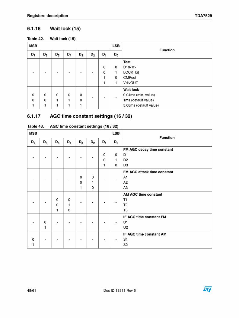
6.1.16 Wait lock (15)
6.1.17 AGC time constant settings (16 / 32)
Table 42. Wait lock (15)
MSB LSBFunction
D7 D6 D5 D4 D3 D2 D1 D0
- - - - - -
0
01
1
0
10
1
TestD18<0>
LOCK_bitCMPout
VdivOUT
0
01
0
01
0
11
0
11
0
01
- - -
Wait lock0.04ms (min. value)
1ms (default value)5.08ms (default value)
Table 43. AGC time constant settings (16 / 32)
MSB LSBFunction
D7 D6 D5 D4 D3 D2 D1 D0
- - - - - -0
0
1
0
1
0
FM AGC decay time constantD1
D2
D3
- - - -00
1
01
0
- -
FM AGC attack time constantA1A2
A3
- -0
01
0
10
- - - -
AM AGC time constantT1
T2T3
- 01
- - - - - -
IF AGC time constant FMU1U2
0
1
- - - - - - -IF AGC time constant AMS1
S2
TDA7529 Registers description
Doc ID 13311 Rev 5 49/61
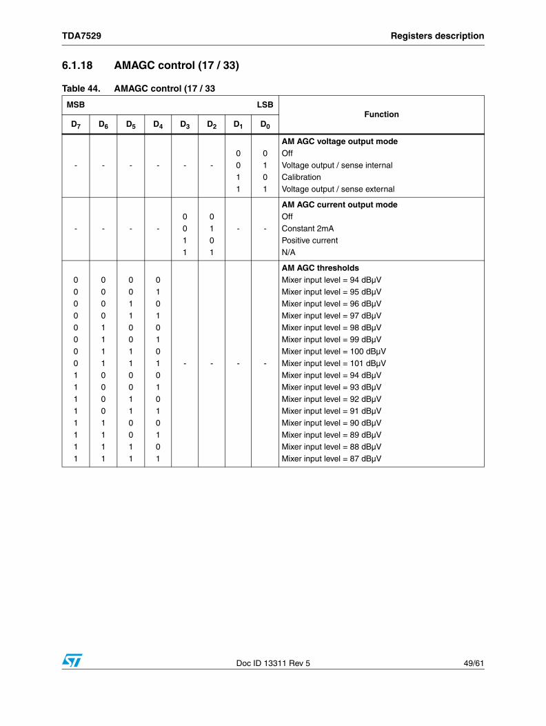
6.1.18 AMAGC control (17 / 33)
Table 44. AMAGC control (17 / 33
MSB LSBFunction
D7 D6 D5 D4 D3 D2 D1 D0
- - - - - -
0
01
1
0
10
1
AM AGC voltage output modeOff
Voltage output / sense internalCalibration
Voltage output / sense external
- - - -
0
01
1
0
10
1
- -
AM AGC current output modeOff
Constant 2mAPositive current
N/A
0
00
0
00
0
01
1
11
1
11
1
0
00
0
11
1
10
0
00
1
11
1
0
01
1
00
1
10
0
11
0
01
1
0
10
1
01
0
10
1
01
0
10
1
- - - -
AM AGC thresholdsMixer input level = 94 dBµV
Mixer input level = 95 dBµVMixer input level = 96 dBµV
Mixer input level = 97 dBµV
Mixer input level = 98 dBµVMixer input level = 99 dBµV
Mixer input level = 100 dBµV
Mixer input level = 101 dBµVMixer input level = 94 dBµV
Mixer input level = 93 dBµV
Mixer input level = 92 dBµVMixer input level = 91 dBµV
Mixer input level = 90 dBµV
Mixer input level = 89 dBµVMixer input level = 88 dBµV
Mixer input level = 87 dBµV
Registers description TDA7529
50/61 Doc ID 13311 Rev 5
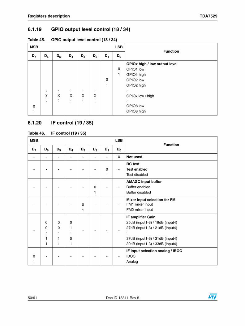
6.1.19 GPIO output level control (18 / 34)
6.1.20 IF control (19 / 35)
Table 45. GPIO output level control (18 / 34)
MSB LSBFunction
D7 D6 D5 D4 D3 D2 D1 D0
01
:
X:
:X:
:X
:
:X
:
:X
:
0
1
0
1
GPIOx high / low output levelGPIO1 lowGPIO1 high
GPIO2 low
GPIO2 high:
GPIOx low / high:
GPIO8 low
GPIO8 high
Table 46. IF control (19 / 35)
MSB LSBFunction
D7 D6 D5 D4 D3 D2 D1 D0
- - - - - - - X Not used
- - - - - - 01
-
RC testTest enabledTest disabled
- - - - - 0
1
- -AMAGC input bufferBuffer enabled
Buffer disabled
- - - - 0
1
- - -Mixer input selection for FMFM1 mixer input
FM2 mixer input
-
0
0:
1
1
0
0:
1
1
0
1:
0
1
- - - -
IF amplifier Gain25dB (input1-3) / 19dB (input4)
27dB (input1-3) / 21dB (input4):
37dB (input1-3) / 31dB (input4)
39dB (input1-3) / 33dB (input4)
01
- - - - - - -
IF input selection analog / IBOCIBOCAnalog
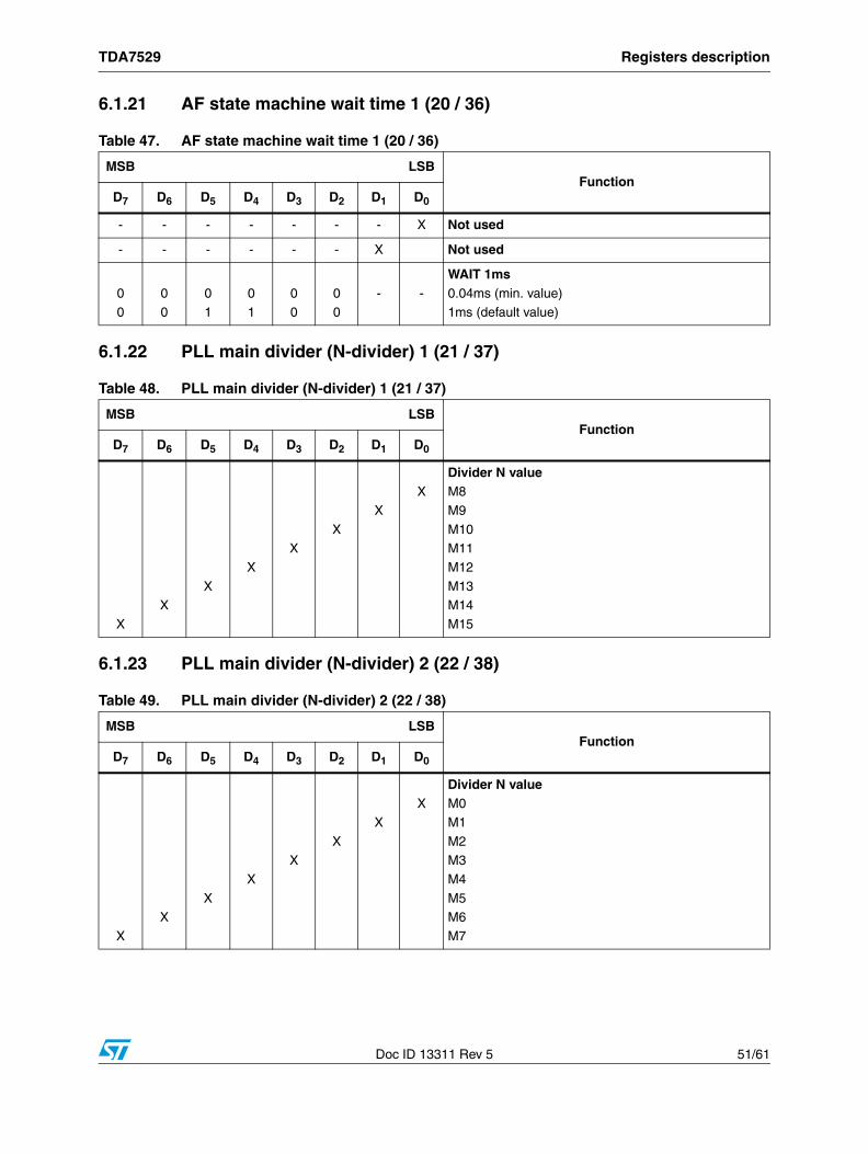
TDA7529 Registers description
Doc ID 13311 Rev 5 51/61
6.1.21 AF state machine wait time 1 (20 / 36)
6.1.22 PLL main divider (N-divider) 1 (21 / 37)
6.1.23 PLL main divider (N-divider) 2 (22 / 38)
Table 47. AF state machine wait time 1 (20 / 36)
MSB LSBFunction
D7 D6 D5 D4 D3 D2 D1 D0
- - - - - - - X Not used
- - - - - - X Not used
00
00
01
01
00
00
- -
WAIT 1ms0.04ms (min. value)1ms (default value)
Table 48. PLL main divider (N-divider) 1 (21 / 37)
MSB LSBFunction
D7 D6 D5 D4 D3 D2 D1 D0
X
XX
X
XX
X
XDivider N valueM8
M9
M10M11
M12
M13M14
M15
Table 49. PLL main divider (N-divider) 2 (22 / 38)
MSB LSBFunction
D7 D6 D5 D4 D3 D2 D1 D0
X
XX
X
XX
X
XDivider N valueM0
M1
M2M3
M4
M5M6
M7
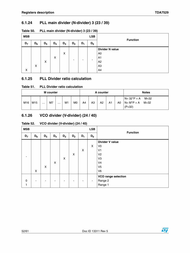
Registers description TDA7529
52/61 Doc ID 13311 Rev 5
6.1.24 PLL main divider (N-divider) 3 (23 / 39)
6.1.25 PLL Divider ratio calculation
6.1.26 VCO divider (V-divider) (24 / 40)
Table 50. PLL main divider (N-divider) 3 (23 / 39)
MSB LSBFunction
D7 D6 D5 D4 D3 D2 D1 D0
X
X
XX
X
- - -
Divider N valueA0
A1A2
A3
A4
Table 51. PLL Divider ratio calculation
M counter A counter Notes
M16 M15 … M7 … M1 M0 A4 A3 A2 A1 A0
N= 32*P + A M=32
N= M*P + A M>32(P=32)
Table 52. VCO divider (V-divider) (24 / 40)
MSB LSBFunction
D7 D6 D5 D4 D3 D2 D1 D0
-
X
X
X
XX
X
XDivider V valueV0
V1
V2V3
V4
V5
V6
01
- - - - - - -
VCO range selectionRange 2Range 1
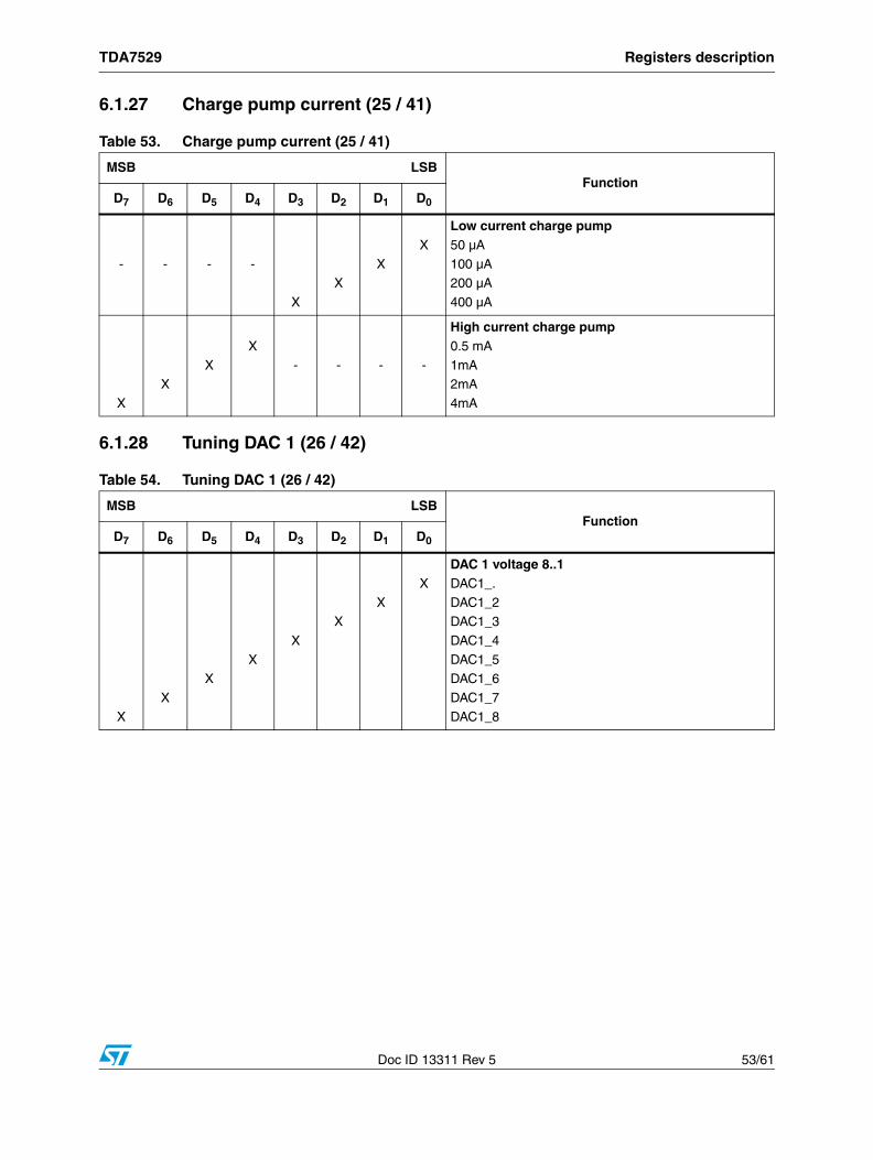
TDA7529 Registers description
Doc ID 13311 Rev 5 53/61
6.1.27 Charge pump current (25 / 41)
6.1.28 Tuning DAC 1 (26 / 42)
Table 53. Charge pump current (25 / 41)
MSB LSBFunction
D7 D6 D5 D4 D3 D2 D1 D0
- - - -
X
XX
X
Low current charge pump 50 µA
100 µA200 µA
400 µA
X
XX
X
- - - -
High current charge pump0.5 mA
1mA2mA
4mA
Table 54. Tuning DAC 1 (26 / 42)
MSB LSBFunction
D7 D6 D5 D4 D3 D2 D1 D0
X
X
XX
X
XX
X
DAC 1 voltage 8..1DAC1_.
DAC1_2DAC1_3
DAC1_4
DAC1_5DAC1_6
DAC1_7
DAC1_8
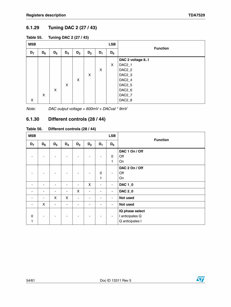
Registers description TDA7529
54/61 Doc ID 13311 Rev 5
6.1.29 Tuning DAC 2 (27 / 43)
Note: DAC output voltage = 600mV + DACval * 9mV
6.1.30 Different controls (28 / 44)
Table 55. Tuning DAC 2 (27 / 43)
MSB LSBFunction
D7 D6 D5 D4 D3 D2 D1 D0
X
X
XX
X
XX
X
DAC 2 voltage 8..1DAC2_1
DAC2_2DAC2_3
DAC2_4
DAC2_5DAC2_6
DAC2_7
DAC2_8
Table 56. Different controls (28 / 44)
MSB LSBFunction
D7 D6 D5 D4 D3 D2 D1 D0
- - - - - - - 0
1
DAC 1 On / OffOff
On
- - - - - - 0
1
-
DAC 2 On / OffOff
On
- - - - - X - - DAC 1_0
- - - - X - - - DAC 2_0
- - X X - - - - Not used
- X - - - - - - Not used
0
1
- - - - - - -IQ phase selectI anticipates Q
Q anticipates I
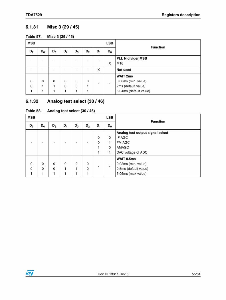
TDA7529 Registers description
Doc ID 13311 Rev 5 55/61
6.1.31 Misc 3 (29 / 45)
6.1.32 Analog test select (30 / 46)
Table 57. Misc 3 (29 / 45)
MSB LSBFunction
D7 D6 D5 D4 D3 D2 D1 D0
- - - - - - -X
PLL N divider MSBM16
- - - - - - X Not used
0
0
1
0
1
1
0
1
1
0
0
1
0
0
1
0
1
1
- -
WAIT 2ms0.08ms (min. value)
2ms (default value)
5.04ms (default value)
Table 58. Analog test select (30 / 46)
MSB LSBFunction
D7 D6 D5 D4 D3 D2 D1 D0
- - - - - -00
1
1
01
0
1
Analog test output signal selectIF AGCFM AGC
AMAGC
DAC voltage of ADC
00
1
00
1
00
1
01
1
01
1
00
1
- -
WAIT 0.5ms0.02ms (min. value)0.5ms (default value)
5.06ms (max value)
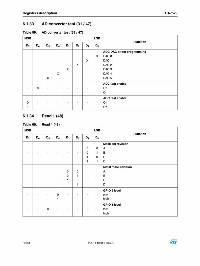
Registers description TDA7529
56/61 Doc ID 13311 Rev 5
6.1.33 AD converter test (31 / 47)
6.1.34 Read 1 (48)
Table 59. AD converter test (31 / 47)
MSB LSBFunction
D7 D6 D5 D4 D3 D2 D1 D0
- -
XX
X
XX
X
ADC DAC direct programmingDAC 0
DAC 1DAC 2
DAC 3
DAC 4DAC 5
- 0
1
- - - - - -ADC test enableOff
On
0
1
- - - - - - -
AGC test enableOff
On
Table 60. Read 1 (48)
MSB LSBFunction
D7 D6 D5 D4 D3 D2 D1 D0
- - - - - -00
1
1
01
0
1
Mask set revisionAB
C
D
- - - -00
1
1
01
0
1
- -
Metal mask revisionAB
C
D
- - - 0
1
- - - -GPIO 5 levellowhigh
- - 01
- - - - -
GPIO 6 levellowhigh
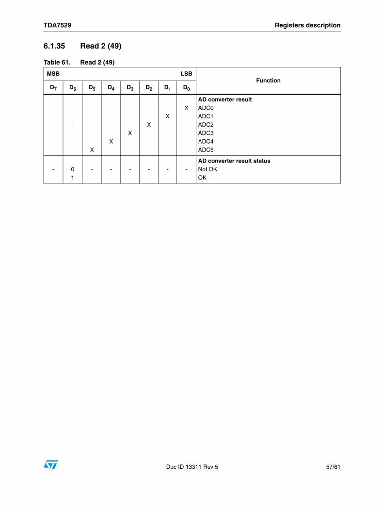
TDA7529 Registers description
Doc ID 13311 Rev 5 57/61
6.1.35 Read 2 (49)
Table 61. Read 2 (49)
MSB LSBFunction
D7 D6 D5 D4 D3 D2 D1 D0
- -
XX
X
XX
X
AD converter resultADC0
ADC1ADC2
ADC3
ADC4ADC5
- 0
1
- - - - - -AD converter result statusNot OK
OK
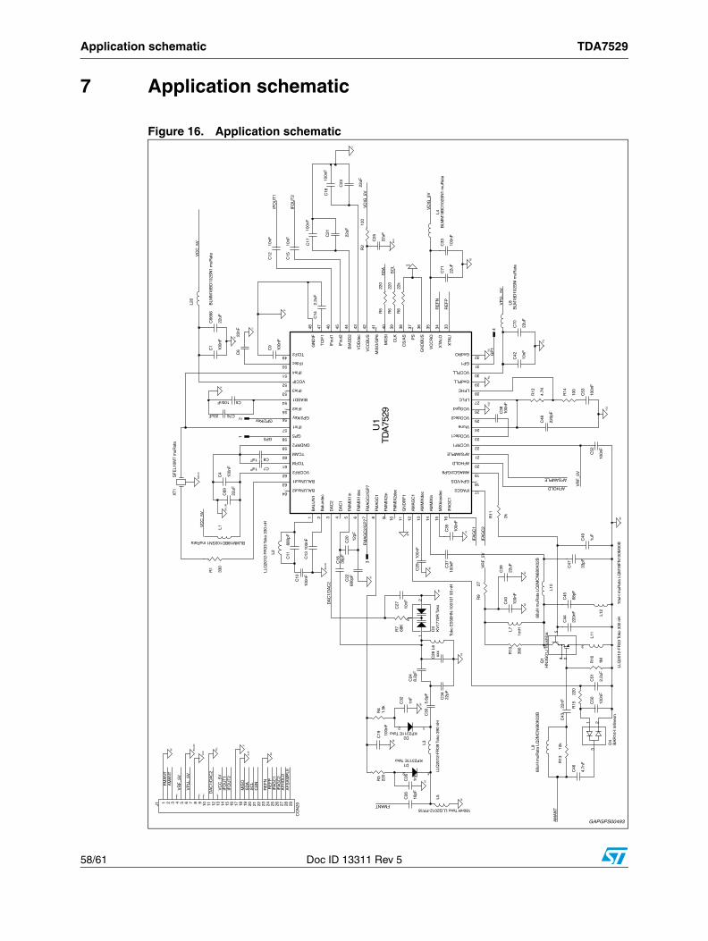
Application schematic TDA7529
58/61 Doc ID 13311 Rev 5
7 Application schematic
Figure 16. Application schematic
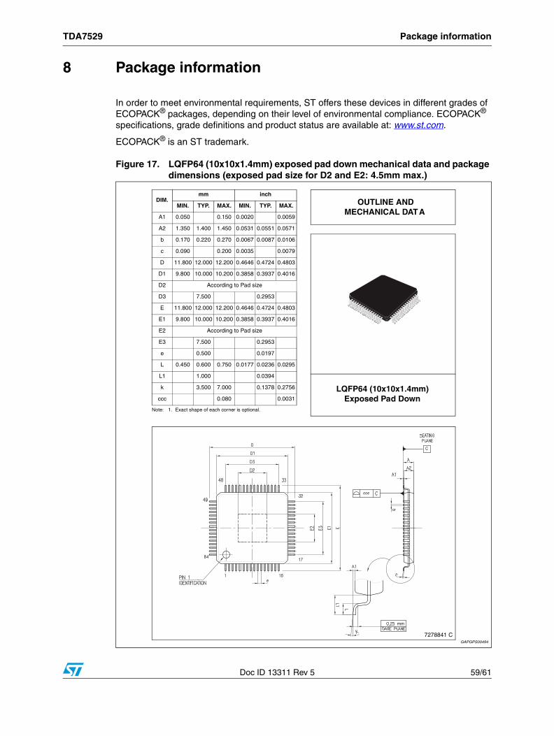
TDA7529 Package information
Doc ID 13311 Rev 5 59/61
8 Package information
In order to meet environmental requirements, ST offers these devices in different grades of ECOPACK® packages, depending on their level of environmental compliance. ECOPACK®
specifications, grade definitions and product status are available at: www.st.com.
ECOPACK® is an ST trademark.
Figure 17. LQFP64 (10x10x1.4mm) exposed pad down mechanical data and package dimensions (exposed pad size for D2 and E2: 4.5mm max.)
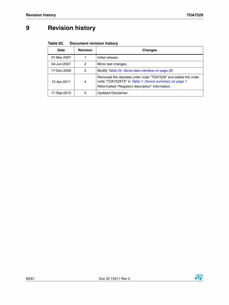
Revision history TDA7529
60/61 Doc ID 13311 Rev 5
9 Revision history
Table 62. Document revision history
Date Revision Changes
07-Mar-2007 1 Initial release.
04-Jun-2007 2 Minor text changes.
17-Dec-2009 3 Modify Table 24: Serial data interface on page 28.
12-Apr-2011 4Removed the obsolete order code “TDA7529” and added the order code “TDA7529TX” in Table 1: Device summary on page 1.
Reformatted “Registers description” information.
17-Sep-2013 5 Updated Disclaimer.
TDA7529
Doc ID 13311 Rev 5 61/61
Please Read Carefully:
Information in this document is provided solely in connection with ST products. STMicroelectronics NV and its subsidiaries (“ST”) reserve theright to make changes, corrections, modifications or improvements, to this document, and the products and services described herein at anytime, without notice.
All ST products are sold pursuant to ST’s terms and conditions of sale.
Purchasers are solely responsible for the choice, selection and use of the ST products and services described herein, and ST assumes noliability whatsoever relating to the choice, selection or use of the ST products and services described herein.
No license, express or implied, by estoppel or otherwise, to any intellectual property rights is granted under this document. If any part of thisdocument refers to any third party products or services it shall not be deemed a license grant by ST for the use of such third party productsor services, or any intellectual property contained therein or considered as a warranty covering the use in any manner whatsoever of suchthird party products or services or any intellectual property contained therein.
UNLESS OTHERWISE SET FORTH IN ST’S TERMS AND CONDITIONS OF SALE ST DISCLAIMS ANY EXPRESS OR IMPLIED WARRANTY WITH RESPECT TO THE USE AND/OR SALE OF ST PRODUCTS INCLUDING WITHOUT LIMITATION IMPLIED WARRANTIES OF MERCHANTABILITY, FITNESS FOR A PARTICULAR PURPOSE (AND THEIR EQUIVALENTS UNDER THE LAWS OF ANY JURISDICTION), OR INFRINGEMENT OF ANY PATENT, COPYRIGHT OR OTHER INTELLECTUAL PROPERTY RIGHT.
ST PRODUCTS ARE NOT DESIGNED OR AUTHORIZED FOR USE IN: (A) SAFETY CRITICAL APPLICATIONS SUCH AS LIFE SUPPORTING, ACTIVE IMPLANTED DEVICES OR SYSTEMS WITH PRODUCT FUNCTIONAL SAFETY REQUIREMENTS; (B) AERONAUTIC APPLICATIONS; (C) AUTOMOTIVE APPLICATIONS OR ENVIRONMENTS, AND/OR (D) AEROSPACE APPLICATIONS OR ENVIRONMENTS. WHERE ST PRODUCTS ARE NOT DESIGNED FOR SUCH USE, THE PURCHASER SHALL USE PRODUCTS AT PURCHASER’S SOLE RISK, EVEN IF ST HAS BEEN INFORMED IN WRITING OF SUCH USAGE, UNLESS A PRODUCT IS EXPRESSLY DESIGNATED BY ST AS BEING INTENDED FOR “AUTOMOTIVE, AUTOMOTIVE SAFETY OR MEDICAL” INDUSTRY DOMAINS ACCORDING TO ST PRODUCT DESIGN SPECIFICATIONS. PRODUCTS FORMALLY ESCC, QML OR JAN QUALIFIED ARE DEEMED SUITABLE FOR USE IN AEROSPACE BY THE CORRESPONDING GOVERNMENTAL AGENCY.
Resale of ST products with provisions different from the statements and/or technical features set forth in this document shall immediately voidany warranty granted by ST for the ST product or service described herein and shall not create or extend in any manner whatsoever, anyliability of ST.
ST and the ST logo are trademarks or registered trademarks of ST in various countries.Information in this document supersedes and replaces all information previously supplied.
The ST logo is a registered trademark of STMicroelectronics. All other names are the property of their respective owners.
© 2013 STMicroelectronics - All rights reserved
STMicroelectronics group of companies
Australia - Belgium - Brazil - Canada - China - Czech Republic - Finland - France - Germany - Hong Kong - India - Israel - Italy - Japan - Malaysia - Malta - Morocco - Philippines - Singapore - Spain - Sweden - Switzerland - United Kingdom - United States of America
www.st.com
Mouser Electronics
Authorized Distributor
Click to View Pricing, Inventory, Delivery & Lifecycle Information: STMicroelectronics:
TDA7529 TDA7529TR