Embed Size (px)
Citation preview

214-0119-01-01_00
R.F. Note #118 Tim Berenc April 24, 1997 John Brandon
John Vincent
RF Control System Characterization INTRODUCTION.......................................................................................................................................2
PHASE REGULATION MODULES ........................................................................................................3
PHASE SHIFTER LINEAR DYNAMIC RESPONSE MEASUREMENTS: ...............................................................3 Current K1200 Phase Shifter ................................................................................................................5 Potential 360° Phase Shifter .................................................................................................................8
PHASE DETECTOR LINEAR DYNAMIC RESPONSE........................................................................................9 Potential 360° Phase Detector ............................................................................................................10 Current K1200 Phase Detector ...........................................................................................................16
K1200 CYCLOTRON: LINEAR DYNAMIC RESPONSE TO PHASE MODULATIONS .......................................17 CCP K500 PREDICTED LINEAR DYNAMIC RESPONSE TO PHASE MODULATIONS .....................................21
DEE VOLTAGE REGULATION MODULES ......................................................................................22
CURRENT K1200 DVR LINEAR DYNAMIC RESPONSE MEASUREMENTS ..................................................23 POTENTIAL DVR LINEAR DYNAMIC RESPONSE MEASUREMENTS............................................................24 K1200 CYCLOTRON: LINEAR DYNAMIC RESPONSE TO VOLTAGE MODULATIONS ...................................25 CCP K500 PREDICTED LINEAR DYNAMIC RESPONSE TO AMPLITUDE MODULATIONS.............................29
CONCLUSION..........................................................................................................................................30
REFERENCES ..........................................................................................................................................30
APPENDIX A ............................................................................................................................................31
THE EFFECT OF THE DEE-TO-DEE COUPLING CAPACITANCE UPON THE DEE VOLTAGE PHASE................31
APPENDIX B.............................................................................................................................................33
MATHEMATICAL DESCRIPTION OF THE CYCLOTRON’S RESPONSE TO ANGULAR MODULATIONS.............33 Narrowband PM..................................................................................................................................35 Wideband PM......................................................................................................................................36
APPENDIX C ............................................................................................................................................37
EFFECT OF THE GAIN BANDWIDTH PRODUCT (GBWP) ON THE CLOSED-LOOP GAIN OF AN OP-AMP.....37
APPENDIX D ...........................................................................................................................................39
EXPERIMENTAL MEASUREMENT DATA ....................................................................................................39

2
Introduction To achieve the desired beam quality from the coupled cyclotrons of the CCP project, the RF amplitude and phase of each cyclotron must be precisely regulated. We are therefore presented with a control problem in providing consistent regulation of these parameters. As with any control system, the system’s stability and accuracy are dependent upon the behavior of the physical modules that measure and maintain the system’s parameters. Thus, before a control topology can be designed, characterizations of the system’s components must be made. Within this RF note, the RF modules which measure and modulate the RF amplitude and phase are characterized. In addition the K1200 cyclotron itself is characterized. What are provided are linear mathematical models describing each individual dynamic response; thus providing a framework with which to design a feedback control system for the critical regulation of the RF voltage and phase. Although a control system is currently in use on the K1200 cyclotron, the CCP requirements are much more stringent. Thus, this RF note presents the characterization of the RF modules which have a high potential of being used within the CCP RF control system. Characterizations of the current K1200 models are included for comparisons to these potential modules. It is important to remember that the new RF modules characterized here are prototypical and may not be used in the final design. The reason why they are being characterized now is to determine whether the fundamental techniques employed in their design will be able to meet the demanding specifications of the CCP project. Once their characterizations are known, the electronics group will be able to design a control topology and determine what the modules’ specifications in terms of thermal drift, etc., need to be in order to meet the requirements for the CCP project. Therefore, soon to follow will be a RF note describing the actual feedback control system topology which we intend to incorporate within the CCP RF system.

3
Phase Regulation Modules In the case of a single cyclotron, the internal dee-to-dee RF phase separation is a constant 120 degrees. For the coupled cyclotron case, an additional constant RF phase, dependent upon the operating beam, will be maintained between the two cyclotrons. Although these phase separations are constant, disturbances and drift within the entire RF system will result in phase variations from these constant settings. Furthermore, the unavoidable dee-to-dee coupling, presented by the central region, links any amplitude modulations on one dee to phase fluctuations on another dee. (For a detailed discussion of this effect, please see Appendix A.) We must therefore provide a control system that maintains constant phase. In order to do this, we use a module to detect phase and a module to change phase. Our entire system therefore consists of the cyclotron itself, along with a phase detector, and a phase shifter. The linear dynamic response of each of these elements was measured experimentally and then modeled mathematically. The actual experimental data for all measurements can be found in Appendix D.
Phase Shifter Linear Dynamic Response Measurements: In order to measure the linear dynamic response of a phase shifter, some sort of phase detection must be used. This seemingly contradicts the separation of the phase shifter and phase detector responses. However, this problem was alleviated by using a Mini-Circuits RPD-1 phase detector. The RPD-1 is basically a double balanced mixer operating in a saturated region as a phase detector. With input signals of identical frequency, its output signal is proportional to the cosine of the phase difference between two input signals plus higher order terms as given by the following formula,
IF output = A A tRF LO1 2 2cos( ) cos( )φ φ ω− + ⋅ + [higher order frequency terms] (1) where A1 2, are amplitudes dependent upon the phase detector, φRF is the phase of the signal at the RF input port, φLO is the phase of the signal at the local oscillator input port, and ω is the frequency of the two signals. By using a simple low-pass filter at the IF output, the second harmonic and the higher order frequency terms can be eliminated. Since the bandwidth of the RPD-1 is much greater than the anticipated bandwidth of the phase shifters, the RPD-1 can be viewed as a perfect measuring instrument except for the non-linear output response imposed by the cosine function. This non-linearity is overcome by centering small phase modulations about 90 degrees. The particular setup used for measuring the linear dynamic response of the phase shifter modules is shown in figure 1.

4
Figure 1: Phase Shifter Linear Dynamic Response Measurement Setup The RF synthesizer provided a signal to the phase shifter for phase modulation, while simultaneously providing a constant phase reference signal to the RPD-1 through the RF power splitter. The output of the low-pass filter was therefore proportional to the phase difference between the phase-modulated signal and the constant phase reference signal. The coaxial cables and the initial phase shift were always chosen so as to center the phase modulations about 90 degrees. The 20 dB attenuating pad was used as a result of the RPD-1 presenting an impedance mismatch while operating in a saturated mode. Furthermore, in order to provide the required 7 dBm signal levels at the RPD-1 inputs in the presence of the attenuators, an amplifier was incorporated. Finally, the 6 dB attenuator merely provided signal level matching at the amplifier inputs. An initial reaction to the above experimental setup would be to think that the amplifier and attenuators would influence the measured response. However, this is not true. The particular amplifier used was a Mini-Circuits ZHL-1A which has a rated bandwidth from 2 MHz to 500 MHz. Furthermore, the attenuators used are rated from DC to 1500 MHz. Since the experimental phase modulations were kept small enough to be considered narrowband phase modulation, the spectrum bandwidth of the phase modulated RF signal was no greater than perhaps twice the phase modulating signal. Furthermore, the injected phase modulating signal never even exceeded 2 MHz for the fastest phase shifter. Thus the occupied spectrum of the phase modulated RF signal was well within the rated bandwidths of the amplifier and attenuators; thereby rendering these devices transparent. By injecting a sinusoidal phase shifting command, ΔΦ IN , both the amplitude and phase of the phase detected signal, ΔΦOUT , relative to this command signal, could be viewed on the oscilloscope. At first, the terminology is quite confusing when talking about the linear dynamic phase response of a phase shifter. However, this confusion is easily remedied by paying close attention to the individual terms. A linear dynamic response has both a magnitude and a phase response as a function of frequency as given by a transfer function of the following form,
AmplifierRF Splitter
6dB Attenuator
Oscilloscope
Ch 2
Phase Shifter
Ch 1
Low-Pass FilterΛΦ
ΛΦ
Signal Generator
20dB AttenuatorRF Synthesizer Mini-Circuits RPD-1

5
G s G s( ) ( )= ∠θ . (2)
In the case of the phase shifter, we wish to determine the linear dynamic response of the phase shifter with respect to its phase shifting input command. Therefore for clarity, the RF phase terms will be denoted with φ and Φ , while the dynamic response phase terms will be denoted with θ . The individual responses for the current K1200 phase shifter, and the potential 360° phase shifter follow. Each magnitude response was normalized with respect to the magnitude response at DC since the input command signals are DC coupled.
Current K1200 Phase Shifter The linear dynamic response of the currently used K1200 phase shifter was measured using the setup discussed above. The results are given in figure 2

6
Figure 2: Current K1200 Phase Shifter Linear Dynamic Response Using an application created within Matlab, a mathematical model was fitted to the above data. The results of the mathematical fit are compared to the experimental data in figure 3. In particular, as can be inferred from figure 2, the current K1200 phase shifter exhibited a double pole at 18 kHz.
101
102
103
104
105
-40
-30
-20
-10
0
Frequency (Hz)
Gai
n (d
B)
Current K1200 Phase ShifterExperimentally Measured Linear Dynamic Response
101
102
103
104
105
-200
-150
-100
-50
0
50
Frequency (Hz)
Phas
e (d
egre
es)

7
Figure 3: Current K1200 Phase Shifter Linear Dynamic Response The transfer function used to produce the mathematical fit was a simple second order system given as
K PS ss
12001279 10
1131 10
10
5 2( ).
( . )=
⋅+ ⋅
, where s j j f= =ω π2
It is natural to question whether the phase shifter’s response is also a function of the RF operating frequency. This was investigated by measuring the linear dynamic response at RF frequencies of 11 MHz, 18 MHz, and 27 MHz. No discrepancies were observed between the linear dynamics responses at these three frequencies. Therefore, it is safe to assume that the above mathematical function characterizes the phase shifter over the cyclotron’s frequency operating range.
101
102
103
104
105
-200
-150
-100
-50
0
50
Frequency (Hz)
Phas
e (d
egre
es)
101
102
103
104
105
-40
-30
-20
-10
0
Frequency (Hz)
Gai
n (d
B)
Current K1200 Phase ShifterComparison of Mathematical Fit to Experimental Data
Experimental DataMathematical Fit

8
Potential 360° Phase Shifter Similarly, the linear dynamic response of the potential 360° phase shifter was experimentally measured using the setup of figure 1. Again, the coaxial cable lengths and the initial phase shift were chosen so as to center the phase modulations about 90°. The Experimentally measured response is shown in figure 4 along with a mathematical fit.
Figure 4: 360° Phase Shifter Linear Dynamic Response As can be seen from the figure, the mathematical model is valid only up to 500 kHz. However, its valid frequency range is well beyond any of our phase detector modules, as will be seen shortly; thus providing a suitable approximation with which to work. Notice the increased bandwidth over the current K1200 phase shifter. The above mathematical fit was based on a sixth order system as given by the following equation,
36015629 10
2 01 10 158 10 133 10 4 84 10 181 10 2 05 10
38
2 6 12 2 6 12 2 6 13PS ss s s s s s
( ).
( . . )( . . )( . . )=
⋅+ ⋅ + ⋅ + ⋅ + ⋅ + ⋅ + ⋅
101 102 103 104 105 106 107-1200
-1000
-800
-600
-400
-200
0
Frequency (Hz)
Phas
e (d
egre
es)
101 102 103 104 105 106 107-100
-80
-60
-40
-20
0
Frequency (Hz)
Gai
n (d
B)
Proposed 360° Phase ShifterComparison of Mathematical Fit to Experimental Data
Experimental DataMathematical Fit

9
As for the magnitude response not matching perfectly at the onset of the ‘break point’, this is of little concern. In a negative feedback system, the closed loop response takes the form of,
G sA s
s A s( )
( )( ) ( )
=+1 β
.
Instabilities occur when the closed loop gain term, β ( ) ( )s A s , has an effective 180° component magnitude greater than or equal to 1. This statement is slightly altered from the usual statement that you can find in the text books. Most books will state that instabilities occur when the closed loop gain term has a magnitude greater than or equal to 1 for the frequency at which it also exhibits a 180° phase shift. By considering the initial statement provided here, we have expanded the definition by considering an effective 180° component. For instance, the closed loop gain term may have a magnitude greater than one at some phase angle less than 180° degrees. By decomposing this into quadrature terms, we obtain the effective 180° component as well as a 90° component. If this effective 180° component actually has a magnitude greater than or equal to 1 instabilities will occur. Our mathematical model above actually ‘over-predicts’ the experimental response by exhibiting a slightly larger gain over the initial ‘break point’. The key point is that the mathematical model accurately predicts both the magnitude and phase term over the valid frequency range. Just as with the current K1200 phase shifter, the functional dependence of the 360° phase shifter response upon the RF operating frequency was investigated. Again, no discrepancies between responses at RF frequencies of 11 MHz, 18 MHz, and 27 MHz were observed.
Phase Detector Linear Dynamic Response In order to measure the linear dynamic response of a phase detector, some sort of phase shifting module must be used. This appears to defeat the objective of separating the responses of the phase shifter and the phase detector. However, a phase detector response could be extracted from a combinational phase shifter plus phase detector response if the phase shifter response was previously known; provided that the phase shifter had a much larger bandwidth than the phase detector. Conveniently, the previously determined phase shifter responses provide such a scenario. Due to the potential 360° phase shifter exhibiting a much larger bandwidth than the current K1200 phase shifter, the former phase shifter was incorporated into the measurements. In particular the measurement setup can be found in figure 5.

10
Figure 5: Phase Detector Linear Dynamic Response Measurement Setup In this setup, the objective is to inject sinusoidal RF phase modulations at the phase shifter in order to determine the phase detector’s response to these modulations. Again, the detected phase difference, ΔΦOUT , will be a phase-shifted sinusoid of the injected ΔΦ IN signal with an amplitude proportional to the gain of the system at that particular frequency. It is again important to note that the phase term of ΔΦOUT , as denoted by θ , is characteristic of the system’s dynamic response and is not describing any RF phase term.
Potential 360° Phase Detector The proposed 360° phase detector has an output which is linearly proportional to the RF phase difference between the two RF signals at its inputs. The linear range extends from -180° to +180°; thus producing a periodic output with a period of 360° as shown in figure 6.
RF Splitter
6dB Attenuator
Phase Detector
Oscilloscope
Ch 2
Phase Shifter
Ch 1
ΛΦ
ΛΦ
Signal Generator
RF Synthesizer

11
Figure 6: Periodic Output Response of the 360° Phase Detector
Due to the linear output response over one period, the phase modulations no longer needed to be restricted around 90° as with the Mini-Circuits phase detector. However, the precaution taken was to restrict the phase modulations from being near to the discontinuous wrap-arounds as seen in the periodic output response of figure 6. For convenience, the phase modulations were centered around an initial RF phase difference of 0°. The experimental measurements can be found in figure 7.
-360 -180 0 180 360 540 720-10
-8
-6
-4
-2
0
2
4
6
8
10
Input RF Phase Difference (degrees)
Δ Φou
t (Vol
ts)
360 ° Phase DetectorPeriodic Output Response

12
Figure 7: 360° Phase Shifter + 360° Phase Detector Combinational Response The fact that transfer function magnitude responses are given in logarithmic form provides a convenient means for combining and extracting individual system responses; especially when considering the additional convenience afforded by using frequency domain representations in the form of LaPlace or Fourier transforms. Transformations from the time domain to the frequency domain conveniently transform the complex operation of convolution into the much simpler operation of multiplication. This is a great advantage in system theory since the response of a system to any input is given by the convolution of that input with the system’s impulse response as given by
y t x t g t( ) ( ) ( )= ⊗ , (3) where y t( ) is the output, x t( ) is the input, and g t( ) is the system’s impulse response. Upon transforming into the frequency domain with LaPlace transforms, the frequency domain output response is merely given as,
Y s X s G s( ) ( ) ( )= ⋅ ,
102
103
104
105
106
-40
-30
-20
-10
0
Frequency (Hz)
Gai
n (d
B)
360° Phase Shifter + 360° Phase DetectorCombinational Dynamic Response
102
103
104
105
106
-500
-400
-300
-200
-100
0
Frequency (Hz)
Phas
e (d
egre
es)

13
where Y s X s G s( ), ( ), ( ) are the LaPlace transforms of the output, input, and system time domain functions respectively. When connecting two systems together in series, as shown in figure 8, the frequency domain response of the combined system is given as,
Y s X s G s G s( ) ( ) ( ) ( )= ⋅ ⋅1 2 . (4)
Figure 8: Combined System Representation The more general way of representing the input to output relationship of such a system is to express it in terms of a transfer function as
Y sX s
G s G s( )( )
( ) ( )= ⋅1 2 (5)
which has both a magnitude response and a phase response expressed as
Y sX s
G s G s G s G s G s G s( )( )
( ) ( ) ( ) ( ) ( ( ) ( ) )= ⋅ = ⋅ ∠ +1 2 1 2 1 2 . (6)
It is now clearly evident why logarithmic magnitudes are used. Since
log( ) log( ) log( )A B A B⋅ = + (7a)
and
log log( ) log( )AB
A B⎛⎝⎜
⎞⎠⎟ = − , (7b)
the logarithmic magnitude response and the phase response of a combinational system are merely given as the addition of the individual responses. Furthermore, when extracting an individual response from a combinational response, the extracted magnitude and phase response is merely given as the subtraction of two responses. Therefore, a combined response given as,
C s G s G s( ) ( ) ( )= ⋅1 2 , (8a) can be expressed as,
G1(s) G2(s)Input X(s) Output Y(s)

14
C s G s G s( ) ( ) ( )= +1 2 , (8b)
∠ = ∠ +∠C s G s G s( ) ( ) ( )1 2 , (8c) where the magnitudes are given as logarithmic magnitudes. On the other hand, if C s( ) and G s1( ) is known, then G s2 ( ) as given by
G sC sG s2
1( )
( )( )
= , (9a)
can be expressed as,
G s C s G s2 1 1( ) ( ) ( )= − (9b)
∠ = ∠ −∠G s C s G s2 1( ) ( ) ( ) . (9c) The above relationships can be used to extract the response of the 360° phase detector from the combinational response of figure 7. Merely subtracting the previously measured response of the 360° phase shifter as shown in figure 4 from the combinational response of figure 7, results in the 360° phase detector response shown below in figure 9. Also included in this figure is the mathematically fit response.

15
Figure 9: 360° Phase Detector Linear Dynamic Response The specific mathematical transfer function estimate for the 360° phase detector response was based upon a 5th order system as given by,
PD ss s s s s
3603113 10
6 912 10 8 796 10 3 948 10 4 273 10 1141 10
28
4 2 5 11 2 5 12( ).
( . )( . . )( . . )=
⋅+ ⋅ + ⋅ + ⋅ + ⋅ + ⋅
.
Similar to the phase shifter dynamic responses, the functional dependence upon the RF operating frequency was investigated. Once again, no discrepancies were observed between the responses at RF frequencies of 11 MHz, 18 MHz, and 27 MHz.
102
103
104
105
106
-400
-300
-200
-100
0
Frequency (Hz)
Phas
e (d
egre
es)
102
103
104
105
106
-40
-30
-20
-10
0
Frequency (Hz)
Gai
n (d
B)
360° Phase DetectorComparison of Mathematical Fit to Experimental Data
Experimental DataMathematical Fit
16
Current K1200 Phase Detector The current K1200 phase detector utilizes two of the RPD-1 Mini-Circuits phase detector that was used for measuring the phase shifter responses. The RPD-1 has a phase detected output that is rated from DC to 50 MHz. However, its response will mainly be limited by the op-amps which are used within the control signal circuitry. A detailed discussion of the frequency response of an op-amp can be found in Appendix C for the interested reader. The material presented there will be highly considered when choosing op-amps for the final control system modules. The particular op-amps used within the current K1200 phase detector were PMI OP-17’s. These op-amps have a typical Gain BandWidth Product (GBWP) of 30 MHz. Even with a gain of 9 these op-amps will still have an extremely high pole frequency of 10 MHz; clearly much faster than the potential 360° phase detector. Although the current K1200 phase detector is faster than the potential phase detector, it has the undesired limited phase detecting range of only -90° to +90°. Furthermore, its output is not linear with phase, but sinusoidal. The potential 360° phase detector has a full range of -180° to +180°. And most importantly, its output is linear over this range. Furthermore, the speed advantage of the current K1200 phase detector does not offer much of an advantage over the potential phase detector because the cyclotron’s response, to be presented later, is the ultimate limiting factor for the control systems.

17
K1200 Cyclotron: Linear Dynamic Response to Phase Modulations It is not adequate to characterize only the phase detector and phase shifter modules. The cyclotron itself is part of the RF control system. Therefore it too should be characterized in terms of its linear dynamic response to phase modulations. This was done by experimentally measuring the combined response of a phase shifter, a phase detector, and the cyclotron as shown in figure 11.
Figure 11: K1200 Cyclotron Phase Response Measurement Setup The RF system of the K1200 cyclotron naturally provided a convenient means by which to measure a single dee subsystem’s response to phase modulations. As shown in the above figure, a RF phase reference is provided to the phase detector through the delay line that follows the phase trimmer module. The second RF output of the phase trimmer module is fed into the phase shifter which then leads to the RF transmitter and the dee resonator. Thus, the experimental setup was identical to the normal operating system of the cyclotron. The phase regulation modules used in the setup were the 360° phase shifter and 360° phase detector. The measurements were performed by injecting sinusoidal phase shifting command signals into the phase shifter and measuring the corresponding output of the phase detector. Therefore, the measured response was representative of the combinational system consisting of the phase shifter, the cyclotron dee, and the phase detector as shown in figure 12. The results of the experimental measurements can be found in figure 13.
Figure 12: Combinational System of the Cyclotron’s Phase Modulation Response
Phase Trimmer
Delay Line
Dee C Subsystem
Dee B SubsystemK1200 Dee A
Dee A Subsystem Phase Detector
Oscilloscope
Ch 2
Phase Shifter
Ch 1
ΛΦ
ΛΦ
Signal Generator
K1200 Freq. Distribution System
360PS (s) Cyc_PR (s)Input X(s) Output Y(s)360PD (s)

18
Figure 13: K1200 Cyclotron RF System Response to RF Phase Modulations
Considering that phase modulating a carrier with a certain signal is equivalent to frequency modulation with the derivative of that signal, and that the cyclotron resonator exhibits a certain quality factor (Q), the bandwidth of the cyclotron’s response to phase modulations can be estimated. The time domain signal representation of a frequency modulated signal is given from [3] as
λ π τ τFM c f
tt A f t k s d( ) cos( ( ) )= ⋅ +⎡
⎣⎢⎤⎦⎥∫2
0 (10)
where f c is the carrier frequency, k f is a proportionality constant relating frequency changes of the cosine term to amplitude values of the modulating signal, s( )τ . The integral of s( )τ is usually denoted by another function g t( ) as given by
101
102
103
104
-30
-25
-20
-15
-10
-5
0
Frequency (Hz)
Gai
n (d
B)
K1200 Cyclotron Dee + 360° Phase Shifter/DetectorLinear Dynamic Response to RF Phase Modulations
101
102
103
104
-250
-200
-150
-100
-50
0
Frequency (Hz)
Phas
e (d
egre
es)
19
g t s dt
( ) ( )≡ ∫0 τ τ . (11)
Therefore, the Fourier transform of g t( ) is related to the Fourier transform of s( )τ by
G fS fj f
( )( )
=2π
. (12)
For narrow band frequency modulation, the FM waveform is reduced by expanding eq (5) using trigonometric identities and keeping the first term of a power series expansion. The expression is given as
λ π π πFM c f ct A f t Ag t k f t( ) cos( ) ( ) sin( )= −2 2 2 . (13)
In conclusion, the narrow-band frequency modulated waveform looks like a transmitted carrier amplitude modulated signal except that the equivalent modulating signal is equal to the integral of the original modulating signal. In the case of phase modulation, g t( ) will be equal to s( )τ , and not its integral. Thus, the process of integration in g t( ) will cancel out the derivative operation on s( )τ . Therefore, narrow-band phase modulation looks almost identical to transmitted carrier amplitude modulation. Of course, as the modulating proportionality constant increases, narrow-band phase modulation transforms to broad-band phase modulation; resulting in an increased bandwidth from the standard transmitted carrier amplitude modulation bandwidth. For a detailed discussion of the above formulations, the interested reader is referred to Appendix A. So how does this pertain to the results that we have observed in measuring the cyclotron’s response to phase modulations? Well, the initial low-frequency sinusoidal phase modulations were kept close to the narrow-band region. The actual modulation index was approximately equal to 2, thus producing a few Bessel function coefficients outside the narrowband case. This would explain the measurement of a second order magnitude response as opposed to the expected first order response for a narrowband case. (For a discussion on this, please see Appendix A). The slight decrease in the experimentally measured response occurring at 5 kHz was a result of increasing the modulation index; thus resulting in the sinusoidal modulating signal occupying an increased bandwidth which in turn was dampened further from the effect of the cyclotron’s quality factor, Q. The modulation index was increased at 5 kHz because the output magnitude was becoming too small to be accurately measured with the oscilloscopes at this frequency. As discussed in Appendix A, our control system should only have to handle narrow-band phase modulations in the presence of noise. Thus we would naturally tend to characterize the cyclotron’s response as a first order system. However, any initial 3 or 4 degree phase offset would put us slightly outside the narrowband case, similar to the experimental measurements. Thus for a safety factor, we will use a second order
20
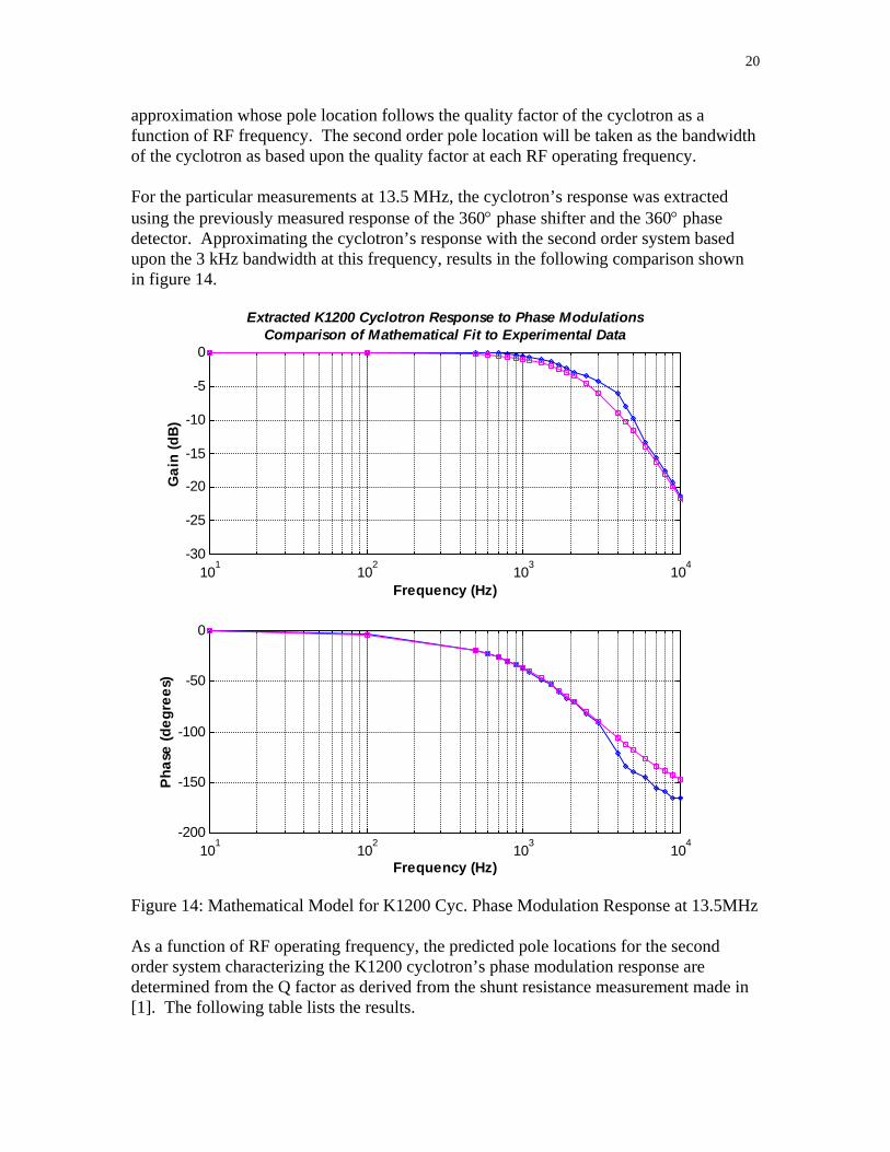
approximation whose pole location follows the quality factor of the cyclotron as a function of RF frequency. The second order pole location will be taken as the bandwidth of the cyclotron as based upon the quality factor at each RF operating frequency. For the particular measurements at 13.5 MHz, the cyclotron’s response was extracted using the previously measured response of the 360° phase shifter and the 360° phase detector. Approximating the cyclotron’s response with the second order system based upon the 3 kHz bandwidth at this frequency, results in the following comparison shown in figure 14.
Figure 14: Mathematical Model for K1200 Cyc. Phase Modulation Response at 13.5MHz As a function of RF operating frequency, the predicted pole locations for the second order system characterizing the K1200 cyclotron’s phase modulation response are determined from the Q factor as derived from the shunt resistance measurement made in [1]. The following table lists the results.
101 102 103 104-30
-25
-20
-15
-10
-5
0
Frequency (Hz)
Gai
n (d
B)
Extracted K1200 Cyclotron Response to Phase ModulationsComparison of Mathematical Fit to Experimental Data
101 102 103 104-200
-150
-100
-50
0
Frequency (Hz)
Pha
se (d
egre
es)

21
Predicted MeasuredFreq (MHz) Q BW (kHz) Pole Location (kHz) Pole Location (kHz)
9.5 5296 1.794 0.89711 5597 1.965 0.98313 5938 2.189 1.095
13.5 ~5500 ~2.4 ~2.4 315 4534 3.308 1.65417 5007 3.395 1.69819 4971 3.822 1.91121 4408 4.764 2.38223 4030 5.707 2.85425 3558 7.027 3.513
26.5 3241 8.177 4.088
Table I: K1200 Cyclotron Pole Location for Phase Modulation Response
K Cyc PM sa
s a1200
22
2
2_ ( )( )
( )=
⋅+ ⋅ππ
, a = Pole Location
The measured pole locations will be filled in as time permits. In the meantime, the control design can proceed based upon the predicted pole locations.
CCP K500 Predicted Linear Dynamic Response to Phase Modulations Similarly, the pole locations for the CCP K500 cyclotron can be predicted from the simulated Q factors given in [2]. The results are given in the following table.
PredictedFreq (MHz) Q BW (kHz) Pole Location (kHz)
11 4232 2.599 2.59913 4133 3.145 3.14515 4080 3.676 3.67617 3971 4.281 4.28119 3827 4.965 4.96521 3659 5.739 5.73923 3483 6.604 6.60425 3305 7.564 7.56427 3001 8.997 8.997
Table II: CCP K500 Predicted Pole Locations for Phase Modulation Response
CCPK PM sa
s a500
22
2
2_ ( )( )
( )=
⋅+ ⋅ππ
, a = Pole Location

22
Dee Voltage Regulation Modules Just as the phase regulation modules have a linear dynamic response to RF phase modulations, the dee voltage regulation module has a linear dynamic response to RF voltage (amplitude) modulations. Since the ability of the voltage regulation module to accurately maintain a constant RF voltage is highly influenced by its dynamic response, it is crucial to characterize this dynamic response. The experimental setup used for measuring the linear dynamic response of a dee voltage regulator was conceptually similar to the setup used for measuring the dynamic response of a phase regulation module. In particular, the experimental setup used is shown in figure 15.
Figure 15: Dee Voltage Regulator Linear Dynamic Response Measurement Setup Both the current K1200 DVR and the potential DVR modules provided a test input into which an amplitude control signal could be injected. Also included on both modules is a dee voltage input port which is normally used for a feedback input signal. A signal proportional to the peak detected RF signal coming into this port is provided as the peak output signal shown in the figure. Therefore, by operating the module in open loop, the dee voltage input port could be used as a peak detected signal of the modules own output; thereby providing a means by which to measure the DVR’s linear dynamic response. With a sinusoidal amplitude control signal at the test input, the peak output would also be a sinusoidal signal with a magnitude and phase relative to the control signal. By sweeping the sinusoidal control signal’s frequency, the linear dynamic response was measured.
DVR RF Out
Peak Output
Oscilloscope
Ch 2
Dee Voltage In
Ch 1
Test Input
Signal Generator
RF Synthesizer

23
Current K1200 DVR Linear Dynamic Response Measurements The linear dynamic response of the DVR currently utilized in the K1200 RF control system was measured using the setup of figure 15. The experimental measurements are shown in figure 16 along with a mathematically fit response.
Figure 16: Current K1200 DVR Linear Dynamic Response The mathematical transfer function used to characterize the K1200 DVR was based upon a 3rd order system as given by
K DVR ss s
12009 922 10
6 283 10 1257 10
14
4 5 2( ).
( . )( . )=
⋅+ ⋅ + ⋅
.
101
102
103
104
105
-250
-200
-150
-100
-50
0
Frequency (Hz)
Phas
e (d
egre
es)
101
102
103
104
105
-50
-40
-30
-20
-10
0
Frequency (Hz)
Gai
n (d
B)
Current K1200 DVRComparison of Mathematical Fit to Experimental Data
Experimental DataMathematical Fit

24
Potential DVR Linear Dynamic Response Measurements The potential DVR model was measured in a manner analogous to the K1200 DVR. Again, the measurement setup of figure 15 was employed. The experimental results are shown in figure 17 along with a mathematically fit response.
Figure 17: Potential DVR Linear Dynamic Response The particular mathematical transfer function used to generate the above response was based upon a 4th order system given by
DVR ss s s s
( ).
( . . )( . . )=
⋅+ ⋅ + ⋅ + ⋅ + ⋅
3 989 102 011 10 1579 10 8 042 10 2 527 10
21
2 5 10 2 5 11
100
101
102
103
104
105
-250
-200
-150
-100
-50
0
Frequency (Hz)
Phas
e (d
egre
es)
100
101
102
103
104
105
-25
-20
-15
-10
-5
0
Frequency (Hz)
Gai
n (d
B)
Proposed DVRComparison of Mathematical Fit to Experimental Data
Experimental DataMathematical Fit
25
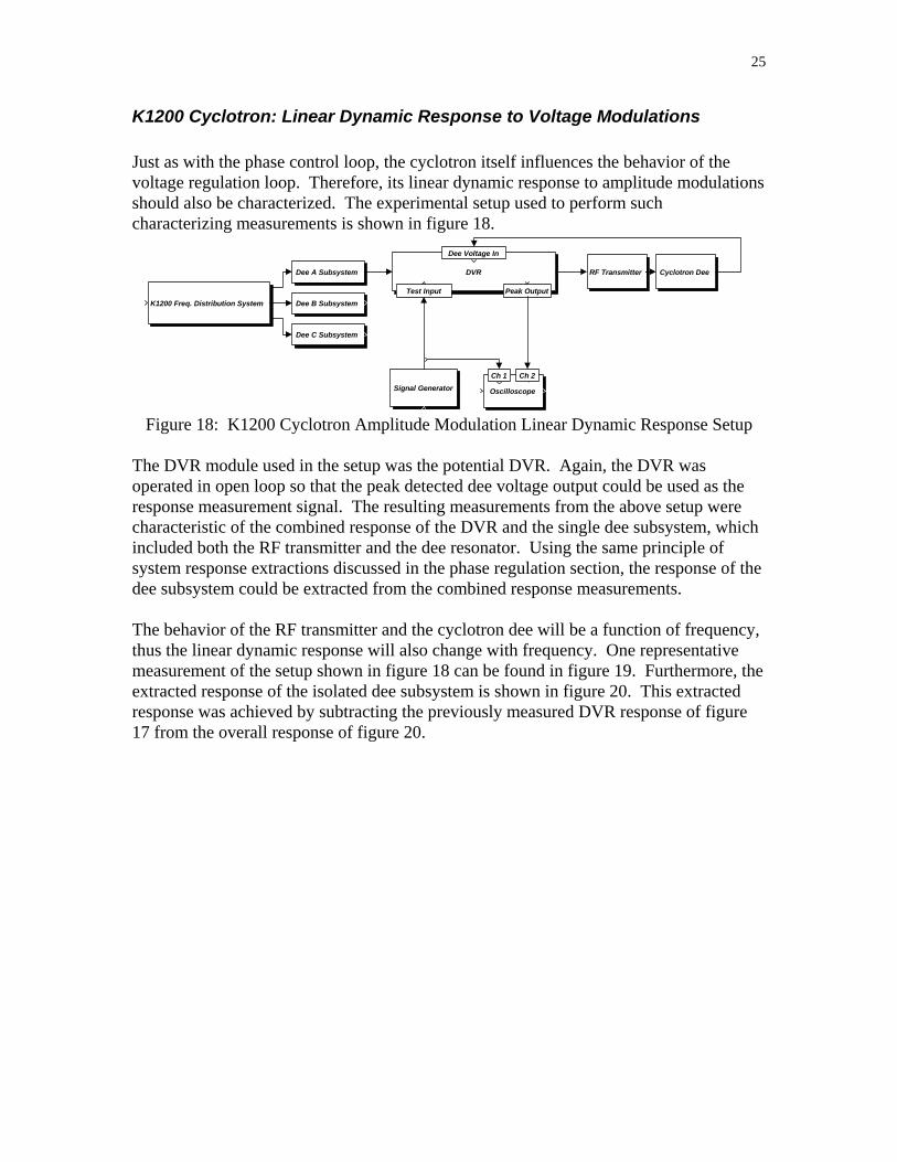
K1200 Cyclotron: Linear Dynamic Response to Voltage Modulations Just as with the phase control loop, the cyclotron itself influences the behavior of the voltage regulation loop. Therefore, its linear dynamic response to amplitude modulations should also be characterized. The experimental setup used to perform such characterizing measurements is shown in figure 18.
Figure 18: K1200 Cyclotron Amplitude Modulation Linear Dynamic Response Setup The DVR module used in the setup was the potential DVR. Again, the DVR was operated in open loop so that the peak detected dee voltage output could be used as the response measurement signal. The resulting measurements from the above setup were characteristic of the combined response of the DVR and the single dee subsystem, which included both the RF transmitter and the dee resonator. Using the same principle of system response extractions discussed in the phase regulation section, the response of the dee subsystem could be extracted from the combined response measurements. The behavior of the RF transmitter and the cyclotron dee will be a function of frequency, thus the linear dynamic response will also change with frequency. One representative measurement of the setup shown in figure 18 can be found in figure 19. Furthermore, the extracted response of the isolated dee subsystem is shown in figure 20. This extracted response was achieved by subtracting the previously measured DVR response of figure 17 from the overall response of figure 20.
Cyclotron Dee
Dee C Subsystem
Dee B Subsystem
DVRDee A Subsystem
Peak Output
Oscilloscope
Ch 2
Dee Voltage In
K1200 Freq. Distribution System
Ch 1
Test Input
Signal Generator
RF Transmitter

26
Figure 19: K1200 + Potential DVR Linear Dynamic Response to Amp. Modulations
101 102 103 104 105-40
-30
-20
-10
0
Frequency (Hz)
Gai
n (d
B)
K1200 Cyclotron + Proposed DVRLinear Dynamice Response to Amplitude Modulations
101 102 103 104 105-400
-300
-200
-100
0
Frequency (Hz)
Pha
se (d
egre
es)

27
Figure 20: Extracted K1200 Cyclotron Response to Amplitude Modulations From the above figure it is easily inferred that the mathematical transfer function is a single order system. The discrepancy between the mathematical fit and the experimental data towards the end of the data is of little concern. The reason is that the individual mathematical models for the DVR and the cyclotron produce a combinational result which accurately predicts the measured combinational response well past the 180° phase response point. Besides, the viewed discrepancy could be a result of accumulative errors from two experimental measurements: the DVR response and the combinational response. For the data shown in figure 20, the single order transfer function is given as,
Cyc VR ss
_ ( ).
( . )=
⋅+ ⋅1131 10
1131 10
4
4
Considering that the cyclotron dee is a resonator, its quality factor is naturally linked to the bandwidth of the amplitude modulation response. This can be understood by considering the above measurement as a modulation and de-modulation process. Injecting amplitude modulations on the dee voltage produces a frequency spectrum centered about the cyclotron’s RF frequency with a bandwidth equal to twice the modulating frequency. Since the cyclotron has a second order bandpass response, the
101
102
103
104
105
-30
-20
-10
0
10
Frequency (Hz)
Gai
n (d
B)
Extracted K1200 Cyclotron Amplitude Modulation ResponseComparison of Mathematical Fit to Experimental Data @ RF = 15 MHz
101
102
103
104
105
-150
-100
-50
0
50
Frequency (Hz)
Phas
e (d
egre
es)

28
amplitude modulated frequency spectrum will be filtered. Furthermore, the de-modulation process of detecting the amplitude response shifts the filtered spectrum down to DC; effectively transforming a second order bandpass response to a first order lowpass response. Thus, the pole location of this first order lowpass response will be intimately related to the cyclotron’s pass band which in turn is described by the cyclotron’s quality factor, Q. In particular, the above measurements would indicate that the cyclotron had a bandwidth of twice the single pole location, or about 3.6 kHz. The actual measured shunt impedance from [1] allowed for the calculation of a corresponding cyclotron bandwidth of 3.3 kHz at a RF frequency of 15 MHz. Therefore, as a function of frequency, the pole locations for the K1200 cyclotron’s linear dynamic response will follow the bandwidth determined by its Q factor. A list of the measured Q factors as determined from [1] is given below. Included is the corresponding pole location for the linear dynamic response transfer function.
Table III: K1200 Pole Locations for Amplitude Modulations
Cyc VR sa
s a_ ( )
( )=
⋅+ ⋅2
2ππ
, a = Pole Location
The quality factors in the above table were determined from the shunt impedance measurements made in [1] for dee A with the simulated shunt capacitance values adjusted by the percent error between the simulated shunt impedance and the measured shunt impedance. Although there was a slight error between the predicted pole location and the measured pole location at an RF frequency of 15 MHz, the predicted pole locations will be adequate for design until time permits for measurements at the various frequencies and on each dee.
Predicted MeasuredFreq (MHz) Q BW (kHz) Pole Location (kHz) Pole Location (kHz)
9.5 5296 1.794 0.89711 5597 1.965 0.98313 5938 2.189 1.09515 4534 3.308 1.654 1.817 5007 3.395 1.69819 4971 3.822 1.91121 4408 4.764 2.38223 4030 5.707 2.85425 3558 7.027 3.513
26.5 3241 8.177 4.088

29
CCP K500 Predicted Linear Dynamic Response to Amplitude Modulations Since the K1200 cyclotron’s response to amplitude modulations was observed to resemble a first order system whose pole location was determined by the Q factor, it is reasonable to assume that the CCP K500 cyclotron will also exhibit this same behavior. Below is a table of these predicted pole locations for the CCP K500 as determined from the simulated Q factors as given in [2].
Table IV: CCP K500 Predicted Pole Locations for Amplitude Modulations
CCPK VR sa
s a500
22
_ ( )( )
=⋅
+ ⋅ππ
, a = Pole Location
PredictedFreq (MHz) Q BW (kHz) Pole Location (kHz)
11 4232 2.599 1.30013 4133 3.145 1.57315 4080 3.676 1.83817 3971 4.281 2.14119 3827 4.965 2.48221 3659 5.739 2.87023 3483 6.604 3.30225 3305 7.564 3.78227 3001 8.997 4.499

30
Conclusion The system characterizations described in this note provide a mathematical framework with which to design both the RF phase and voltage feedback control systems for the Coupled Cyclotron Project. As was observed, the linear dynamic responses of the phase and voltage regulation modules do not exhibit any dependence upon the operating RF frequency; however, linear dynamic responses of both the CCP K500 and the K1200 do exhibit a dependence upon the RF operating frequency. This RF frequency dependence will be taken into account when designing the RF control system. Soon to follow will be a RF note covering the actual control system design. References [1] J. Vincent, Modeling and Analysis of Radio Frequency Structures using an Equivalent Circuit Methodology with Application to Charged particle Accelerator RF Resonators, A dissertation submitted to Michigan State University, Department of Electrical Engineering, 1996. [2] T. Berenc and J. Vincent, CCP K500 Tuning Stem Design, an NSCL RF Note
#116, November 1996. [3] M. S. Roden, Analog and Digital Communication Systems, 3rd Edition, Prentice Hall, New Jersey, 1991. [4] G. Franklin, J. Powell, A. Emami-Naeini, Feedback Control of Dynamic Systems, 3rd Edition, Addison-Wesley Publishing Co., 1994. [5] Spectrum Analysis: Amplitude and Frequency Modulation, A Hewlett Packard Test & Measurement Application Note 150-1. [6] A. Sedra, K. Smith, Microelectronic Circuits, 3rd Edition, Saunders College Publishing, New York, 1991.

31
Appendix A
The Effect of the Dee-to-Dee Coupling Capacitance Upon the Dee Voltage Phase
One of the most often misconstrued ideas about the phase separation between the cyclotron dees is that this phase separation should remain constant without need for feedback control. This idea is false. Besides any 60Hz noise and other disturbances in the phase modules, the dee-to-dee coupling capacitance links amplitude fluctuations to phase fluctuations. To understand why this occurs we will consider a first order case of two identical parallel RLC resonators coupled together through a series capacitance as in figure 1. The above circuit has two modes of resonance; a ‘push-push’ and a ‘push-pull’ mode. In the ‘push-push’ mode, the resonators oscillate in phase with each other at the same natural frequency as an isolated resonator; thus the coupling capacitor has no effect on the resonant frequency of this mode. In the ‘push-pull’ mode, the resonators oscillate 180° out of phase with respect to one another at a frequency which is lower than the natural resonance of an isolated resonator. The frequency separation of the two modes is determined by the amount of coupling between the resonators. The larger the capacitance, the larger the energy maintained by the coupling element. Since the rate at which energy can be transferred to each resonator is fixed by the resonator components, the amount of energy maintained by the coupling element will influence the amount of time required to transfer this energy. Thus, for a larger amount of energy maintained within the coupling element, the longer it takes for this energy to be transferred back and forth between the coupling element to each resonator. Therefore, the larger the coupling element, the lower the frequency and the larger the frequency separation between the ‘push-push’ and ‘push-pull’ modes. In the case of the cyclotron, we are driving each resonator separately at its natural resonate frequency with a 120° phase separation between each resonator. Due to the dee-to-dee capacitive coupling which unavoidable exists near the central region, each dee will couple an in phase component to its adjacent dees. The component is in phase since the isolated resonate frequency of a dee corresponds to the ‘push-push’ mode. Considering the first order case of only two dees coupled together, the voltage on dee-1 will be a
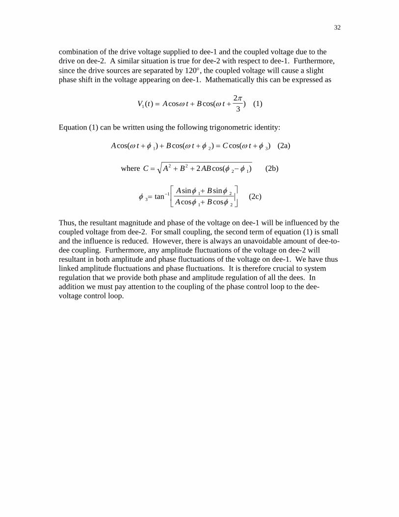
32
combination of the drive voltage supplied to dee-1 and the coupled voltage due to the drive on dee-2. A similar situation is true for dee-2 with respect to dee-1. Furthermore, since the drive sources are separated by 120°, the coupled voltage will cause a slight phase shift in the voltage appearing on dee-1. Mathematically this can be expressed as
V t A t B t1
23
( ) cos cos( )= + +ω ωπ
(1)
Equation (1) can be written using the following trigonometric identity:
A t B t C tcos( ) cos( ) cos( )ω φ ω φ ω φ+ + + = +1 2 3 (2a)
where C A B AB= + + −2 22 12 cos( )φ φ (2b)
φφ φφ φ3
1 1 2
1 2=
++
⎡
⎣⎢
⎤
⎦⎥
−tansin sincos cos
A BA B
(2c)
Thus, the resultant magnitude and phase of the voltage on dee-1 will be influenced by the coupled voltage from dee-2. For small coupling, the second term of equation (1) is small and the influence is reduced. However, there is always an unavoidable amount of dee-to-dee coupling. Furthermore, any amplitude fluctuations of the voltage on dee-2 will resultant in both amplitude and phase fluctuations of the voltage on dee-1. We have thus linked amplitude fluctuations and phase fluctuations. It is therefore crucial to system regulation that we provide both phase and amplitude regulation of all the dees. In addition we must pay attention to the coupling of the phase control loop to the dee-voltage control loop.

33
Appendix B
Mathematical Description of the Cyclotron’s Response To Angular Modulations
How do we mathematically describe the cyclotron’s response to angular modulation? Well, we know the amplitude response of the cyclotron as a function of frequency due to its resonate behavior which can be expressed as a second order system. We also can mathematically describe the frequency spectrum of a sinusoidally frequency modulated waveform. Let’s begin with a sinusoidal carrier representative of the cyclotron’s unmodulated RF signal:
λ ω φ( ) cos( ) cos( ( ))t A t A tc o= + = Φ (1) where φo represents a constant phase offset which we will set to zero for convenience, ωc is the unmodulated carrier frequency, and A is an arbitrary amplitude. When we begin to modulate the phase term, the phase becomes a function of time and the waveform can be expressed as
λ ω φPM ct A t t( ) cos( ( ) )= + (2).
Equation (2) represents a waveform whose phase is a function of time. Based upon the definition of instantaneous frequency, the phase modulations correspond to frequency modulations. To see this let us consider the definition of frequency. In equation (1), the term in parantheses represents a phase angle. The time rate of change of that phase angle actually represents the frequency of the signal. Mathematically, this fact is expressed as,
ωi
ddt
=Φ
(3).
When we consider a pure sinusoidal waveform with a constant phase offset as given in equation (1), how was the ωc term derived in the first place. Looking at how a sinusoidal waveform is generated will help to understand the relationship between frequency and phase as expressed in eq.(3). The definitions of the sine and cosine functions are based upon the projections of a unit vector at an arbitrary phase angle upon quadrature axes. A sinusoidal waveform is generated by rotating the phase angle term around the unit circle at a periodic rate or

34
frequency. Therefore, if we rotate the unit vector so that we make 1 revolution in T seconds, then the angular rotation rate is expressed in terms of radians as
ωπ
=2T
(4)
And at any specific time, t, the value of the sinusoidal function can be evaluated from the phase angle argument given as
φ ω= t (5)
It is now clearly seen that the angular frequency is that given in equation (3). When the phase of the cyclotron is dynamically changed, the cyclotron’s waveform can be expressed as:
λ ωPM ct A t K s t( ) cos( ( ))= + 1 (6)
where s t( ) is the phase angle modulating signal and K1 is a proportionality constant known as the modulation index. It is dependent upon the phase modulating device. For further insight into phase modulation, let us consider the case when the modulating signal is sinusoidal or
s t tM( ) sin( )= ω (7)
where ωM is the frequency of the modulating signal. Thus the instantaneous frequency, using equation (3), becomes,
ω ω ω ωi c M Mt K t( ) cos( )= + 1 (8)
Furthermore, the phase modulated waveform takes the form
λ ω ωPM c Mt A t K t( ) cos( sin )= + 1 (9).
Thus K1 , the modulation index, represents the maximum phase shift of the carrier and ωM K1 represents the maximum frequency deviation from the carrier frequency.

35
Narrowband PM For narrowband PM, we will assume that K1 is small such that a sine and a cosine term of K1 can be represented by the first term of a MacLaurin series. Using the trigonometric identity of
cos( ) cos cos sin sinA B A B A B± = m (10),
equation (9) can be written as
λ ω ω ω ωPM c M c Mt A t K t A t K t( ) cos cos( sin ) sin sin( sin )= −1 1 (11)
Now for K1 small, equation (11) can be reduced to
[ ]λ ω ω ωPM c c Mt A t K t t( ) cos sin sin= − ⋅1 (12)
Equation (12) looks like a transmitted carrier amplitude modulated waveform except that the lower sideband produced by (12) has a reversed phase from the amplitude modulation case. Therefore, the resultant sideband vector is always in phase quadrature for narrowband as opposed to in-phase for amplitude modulation. Thus, besides producing phase variations, narrowband PM also appears to produce small amplitude changes as well. Since the narrowband PM waveform will have the same frequency spectrum as a Double Sideband Transmitted Carrier Amplitude Modulated (DSTC AM) waveform, the cyclotron’s response to small phase modulations will be identical to the cyclotron’s response to amplitude modulations. Since the cyclotron is a second order resonator, this response is a first order system whose pole is determined from the resonator’s Q factor as discussed in the RF note. The narrowband approximation will suffice for our control system since during normal operations, the control system will be responding to small noise phase modulations which should satisfy the requirements of narrowband PM. The measurements presented within the RF note were the result of a modulation index equal to 2-4. When the modulation becomes greater than 1, the narrowband approximation begins to fail and we must perform a wideband PM analysis. For the sake of design, we will approximate the cyclotron’s phase response with a second order system whose pole is not equal to half of the resonator’s bandwidth, but whose pole is equal to the full resonator’s bandwidth. Although the system noise should satisfy requirements for the narrowband case, the second order approximation will allow for system stability during any initial 3-4 degree phase errors. If a control system is designed to be stable for the second order approximation, it will most definitely be stable for the single order approximation of narrowband PM.

36
Wideband PM For wideband PM, we must work with the base form of the PM waveform as given in eq.(9) repeated here:
λ ω ωPM c Mt A t K t( ) cos( sin )= + 1 (9)
This is an analysis of a single sinusoidal modulating signal. To simplify the analysis, the PM waveform is expressed in exponential notation as
{ }λ ω ωPM
j t jK tt Ae ec M( ) Re= 1 (13)
The second exponential function of equation (13) is periodic with period 2πωM
. It can
thus be expanded into a complex Fourier Series given as
e c ejK tn
jn tM M1 sinω ω=−∞
+∞
∑ (14)
where the Fourier coefficients can be computed as
c e e dtnM jK t jn tM M
M
M
= −
−
+
∫ωπ
ω ω
πω
πω
21 sin (15)
The above equation is a function of n and K1 and is well known as an integral representation of the nth order Bessel function of the first kind. In wideband PM, what happens is that the frequency spectrum of the PM waveform becomes an infinite series of discrete frequency components separated in frequency by ωM and with a magnitude equal to a coefficient given by a Bessel function. For a small modulation index, the magnitudes of the coefficients decay rapidly as n increases and thus only a few frequency components exist within the spectrum of the PM waveform. For a large modulation index, the coefficients do not decay as rapidly and more coefficients must be included; resulting in a wider frequency spectrum for the PM waveform. In the case of the cyclotron, as the modulation index increases, the bandwidth of the resultant waveform increases, and the cyclotron’s resonate response attenuates some of these frequency components; thus producing a rather complex frequency response to phase modulations. A more detailed account of wideband PM can be found in the references. We are assuming that our phase noise will be within the narrowband case; therefore, the wideband case will not be investigated any further at this point.
37
Appendix C
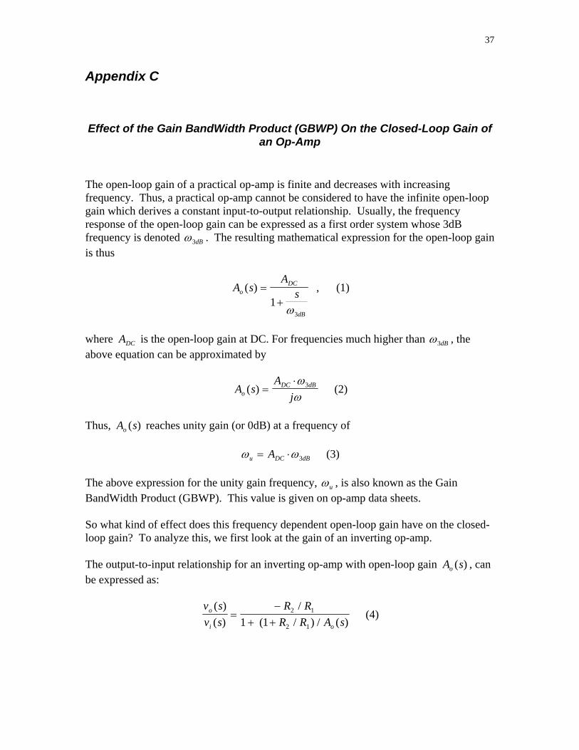
Effect of the Gain BandWidth Product (GBWP) On the Closed-Loop Gain of an Op-Amp
The open-loop gain of a practical op-amp is finite and decreases with increasing frequency. Thus, a practical op-amp cannot be considered to have the infinite open-loop gain which derives a constant input-to-output relationship. Usually, the frequency response of the open-loop gain can be expressed as a first order system whose 3dB frequency is denoted ω3dB . The resulting mathematical expression for the open-loop gain is thus
A sA
soDC
dB
( ) =+1
3ω
, (1)
where ADC is the open-loop gain at DC. For frequencies much higher than ω3dB , the above equation can be approximated by
A sA
joDC dB( ) =
⋅ωω
3 (2)
Thus, A so ( ) reaches unity gain (or 0dB) at a frequency of
ω ωu DC dBA= ⋅ 3 (3)
The above expression for the unity gain frequency, ωu , is also known as the Gain BandWidth Product (GBWP). This value is given on op-amp data sheets. So what kind of effect does this frequency dependent open-loop gain have on the closed-loop gain? To analyze this, we first look at the gain of an inverting op-amp. The output-to-input relationship for an inverting op-amp with open-loop gain A so ( ) , can be expressed as:
v sv s
R RR R A s
o
i o
( )( )
/( / ) / ( )
=−
+ +2 1
2 11 1 (4)

38
This equation reduces to the familiar inverting gain equation when A so ( ) becomes the ideal infinite case for all frequencies. Substituting eq.(2) into eq.(4) and using the expression of eq.(3) we obtain:
v sv s
R RR RA
sR R
o
i
DC u
( )( )
/( / )
/ ( / )
=−
++
++
2 1
2 1
2 11
11ω
(5)
In typical applications A R RDC >> +( / )1 2 1 , thereby reducing equation (5) into
v sv s
R RsR R
o
i
u
( )( )
/
/ ( / )
=−
++
2 1
2 11
1ω
(6)
Therefore, the inverting op-amp gain has a single order pole which is a function of the DC gain of R R2 1/ . The 3dB frequency is thus seen to be
ωω
CL dBu
R R32 11
=+( / )
(7)
Thus as the DC gain is increased, the pole gets smaller; thereby deteriorating the frequency response. A similar analysis of the non-inverting configuration will give an identical 3dB frequency as in eq(6). However, the non-inverting configuration is usually used as a buffer amp with R2 0= . Thus the 3dB frequency will be equal to the GBWP frequency for a buffer amp. Furthermore, when we chain n op-amps in series, the overall response will thus have n poles at the 3dB frequency given by eq.(6). The current K1200 modules use PMI OP-17 op-amps whose GBWP is rated at 30 MHz. The typical number of op-amps used in series within these modules is around 3, each at approximately unity gain. Thus, the overall response due to the op-amps would be 3 poles at a frequency of 15 MHz; clearly much faster than the responses that were measured for current K1200 Phase Shifter. The potential RF modules use PMI OP-400 op-amps whose GBWP is only 500 kHz. When measuring the response of these modules, all op-amp gains were set to unity, therefore producing a 3dB frequency close to 250 kHz for each op-amp. The typical number of series op-amps for the potential RF modules was 3. The potential 360° phase detector magnitude response was not even measured far beyond the 25 kHz point at which the op-amp phase response would kick in. However, the potential 360° phase shifter had a measurable response well up to 2 MHz. Thus, it is reasonable to assume that the measured response was mainly due to its op-amps.

39
Appendix D
Experimental Measurement Data