Embed Size (px)
Citation preview
1
Reviewofwidebandgapchalcogenidesemiconductors
Rachel Woods-Robinson1,2,3$, Yanbing Han4,1$, Hanyu Zhang1, Tursun Ablekim1, Imran Khan1,
Kristin Persson2,3, Andriy Zakutayev1* 1. Materials and Chemical Science and Technology Directorate, Golden, CO 80401, USA
2. Department of Applied Science and Technology, University of California, Berkeley, CA 94720, USA
3. Materials Sciences Division, Lawrence Berkley National Laboratory, Berkeley, CA 94720, USA
4. School of Physics, Zhengzhou University, Zhengzhou 450052 China
* Corresponding Author: [email protected] $ Rachel Woods-Robinson and Yanbing Han contributed equally to this review
Abstract Wide band gap semiconductors are essential for today’s electronic devices and energy applications due to their high optical transparency, as well as controllable carrier concentration and electrical conductivity. There are many categories of materials that can be defined as wide band gap semiconductors. The most intensively investigated are transparent conductive oxides (TCOs) such as tin-doped indium oxide (ITO) and amorphous In-Ga-Zn-O (IGZO) used in displays, carbides (e.g. SiC) and nitrides (e.g. GaN) used in power electronics, as well as emerging halides (e.g. g-CuI) and 2D electronic materials (e.g. graphene) used in various optoelectronic devices. Compared to these prominent materials families, chalcogen-based (Ch = S, Se, Te) wide band gap semiconductors are less heavily investigated but stand out due to their propensity for p-type doping, high mobilities, high valence band positions (i.e. low ionization potentials), and broad applications in electronic devices such as CdTe solar cells. This manuscript provides a review of wide band gap chalcogenide semiconductors. First, we outline general materials design parameters of high performing transparent conductors, as well as the theoretical and experimental underpinnings of the corresponding research methods. We proceed to summarize progress in wide band gap (EG > 2 eV) chalcogenide materials, such as II-VI MCh binaries, CuMCh2 chalcopyrites, Cu3MCh4 sulvanites, mixed anion layered CuMCh(O,F), and 2D materials, among others, and discuss computational predictions of potential new candidates in this family, highlighting their optical and electrical properties. We finally review applications of chalcogenide wide band gap semiconductors, e.g. photovoltaic and photoelectrochemical solar cells, transparent transistors, and light emitting diodes, that employ wide band gap chalcogenides as either an active or passive layer. By examining, categorizing, and discussing prospective directions in wide band gap chalcogenides, this review aims to inspire continued research on this emerging class of transparent conductors and to enable future innovations for optoelectronic devices.
2
TableofContents 1. Introduction 2. Methods 2.1 Synthesizability and Stability 2.1.1 Thermodynamic stability calculations 2.1.2 Experimental synthesis and phase purity 2.2 Band gap. 2.2.1 Computational optical properties 2.2.2 Experimental optical properties 2.3 Mobility and Conductivity. 2.3.1 Effective mass and scattering time. 2.3.2 Mobility and Conductivity Measurements 2.4 Dopability 2.4.1 Computational dopability 2.4.2. Experimentally quantifying doping. 2.5 Band positions, alignments, and other properties. 2.5.1 Computational band alignment 2.5.2 Experimental band alignment 3. Materials 3.1 Binary II-Ch Chalcogenides 3.1.1 ZnCh. 3.1.2 MgCh. 3.1.3 MnCh 3.1.4 CdCh 3.1.5 BeCh 3.1.6 CaCh 3.1.7 II-VI Alloys and composites 3.2. Other binary Mx-Chy chalcogenides 3.3 Ternary chalcopyrite Ib-III-Ch2 compounds 3.3.1 Cu(Al,Ga)Ch2 3.3.2 Ag(Al,Ga)Ch2 3.3.3. I-III-Ch2 alloys. 3.4 Other Ternary Chalcogenides 3.4.1 α-BaM2Ch2, Pnma structure
3.4.2 Cu3MCh4, Sulvanite and sulvanite-like 3.4.3 ABCh2, Delafossites. 3.4.4 ABCh3, Perovskites. 3.4.5 A2B3Ch4 and Dimensional reduction. 3.4.6 A3BCh3 and other ternaries 3.5 Quaternary and mixed anion chalcogenides 3.5.1 LnCuOCh 3.5.2 MCuChF(M=Ba, Sr). 3.5.3 MSCN. 3.5.4 Quintenary layered compounds. 3.5.5 Computationally predicted oxychalcogenides 3.5.6 Quaternary single-anion compounds. 3.6 2D chalcogenides 3.6.1 Transition-metal Chalcogenides (TMC) 3.6.2 Post Transition-metal Chalcogenides (PTMC) 3.6.3 Metal Phosphorus Trichalcogenides (MPT) 3.7 Summary of optoelectronic properties 4. Applications 4.1 Solar cells 4.1.1 CdTe solar cells 4.1.2 CIGS solar cells. 4.1.3 Additional PV applications 4.2 Other Devices 4.2.1 Transparent thin film transistors 4.2.2 Water splitting photocatalysts and photoabsorbers 4.2.3 Diodes 4.3 Summary of band Offsets for Devices 5. Summary and Outlook Acknowledgements References
3
1.Introduction Wide band gap (WBG) semiconductors are critical to various electronic devices such as transparent contacts, p-n junctions, and thin film transistors.1 Since the 1950s, oxide wide band gap semiconductors have been intensively investigated, in particular for their contradicting properties of high transparency and high conductivity. The transparent conducting oxide (TCO) Sn-doped In2O3, known as ITO, has been paramount to a variety of commercial devices in the past decades.2 Possible alternatives such as F-doped SnO2 (FTO)3 and Al-doped ZnO (AZO)4 have been also explored in-depth and implemented into commercial devices. Multinary transparent amorphous oxide semiconductors (TAOS) such as indium zinc gallium oxide (IGZO) have also been heavily investigated during the 21st century as channel layers in thin film transistors (TFT) due to their high transparency, high mobility, and good uniformity,5 leading to their commercial use in liquid crystal displays (LCDs).
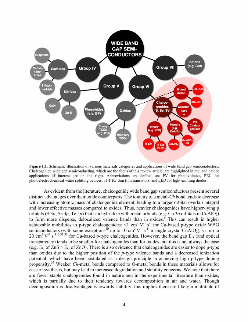
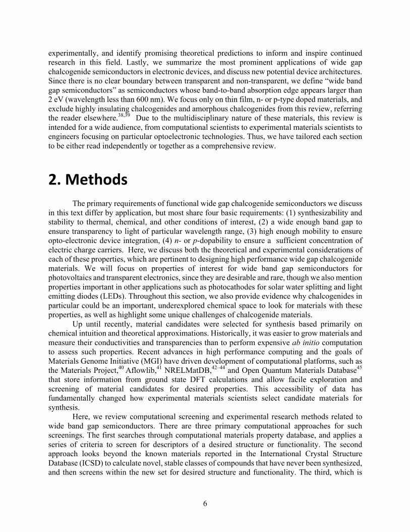
Although these n-type TCOs show excellent performance, p-type doping in such materials has proven much more difficult to achieve in practice. This is due primarily to (1) intrinsic limitations in dispersion that localize the valence band holes, and (2) challenges in introducing the holes by p-type doping and minimizing compensating defects. A breakthrough was achieved when the strategy of “chemical modulation of the valence band” (CMVB) was proposed, using delafossite CuAlO2 as a preliminary example.6 This approach uses hybridization of O 2p states with metal 3d states in the valence band, increasing dispersion. Subsequently, different kinds of copper based p-type TCOs have been reported using this strategy and other approaches, though optoelectronic properties of p-type TCOs still do not compare with n-type TCOs. Due to these challenges, only a narrow subset of p-type TCO materials have been incorporated into device applications even in the lab, e.g. Cu2O and SnO, which are mainly used in thin film transistors (TFTs) .7 Despite the focus of research and device integration on wide gap oxide materials, transparent conductors are not limited to oxides. To date (2019), there are several classes of non-oxide semiconductors that have been demonstrated experimentally to be transparent and conducting. The following group VI-based semiconductors, which are of interest in this review, have been investigated: (1) Binary II-VI type semiconductors (e.g. ZnS,8 CdS,9 ZnxCd1-xS10), as well as other binary Mx-VIy semiconductors (e.g. SnS2, In2S3); (2) Ternary chalcopyrite I-III-VI2 semiconductors (mostly copper-based), represented by CuAlS2,11 a-BaCu2S2,12 and Cu3TaS4;13 (3) Multinary layered mixed-anion compounds, such as LaCuOCh,14 BaCuSF, and CuSCN15 (3) 2D chalcogenides, such as MoS2, including both binary and ternary materials. In addition, there has also been significant research on wide band gap semiconductors (i.e. WBG semiconductors or WBGSs) with anions from groups IV (e.g. graphene,16 and carbon nanotubes,17 SiC)18, V (e.g. GaN,19,20 zinc nitrides21), and VII (e.g. CuI22), which are not discussed here. A network diagram of these classes of materials are displayed schematically in Figure 1.1. There have been many review papers and book chapters addressing different aspects of this broad field of WBG semiconductors. Some address oxide TCOs, focusing on intrinsic material properties23,24, while others highlight applications such as transparent electronics,1 TFTs,7 and photovoltaics.25 Others summarize nitrides,26 halides,22 and carbides,27 including graphene.28 A few reviews have briefly mentioned wide gap chalcogenide semiconductors, but limit their focus to oxides or a narrow subset of chalcogenides.29 Herein chalcogen anions are referred to as “Ch”, with Ch = S, Se, Te, and not including oxygen O for the purposes of this article.
4
Figure 1.1. Schematic illustration of various materials categories and applications of wide band gap semiconductors. Chalcogenide wide gap semiconducting, which are the focus of this review article, are highlighted in red, and device applications of interest are on the right. Abbreviations are defined as: PV for photovoltaics, PEC for photoelectrochemical water splitting devices, TFT for thin film transistors, and LED for light emitting diodes.
As evident from the literature, chalcogenide wide band gap semiconductors present several
distinct advantages over their oxide counterparts. The ionicity of a metal-Ch bond tends to decrease with increasing atomic mass of chalcogenide element, leading to a larger orbital overlap integral and lower effective masses compared to oxides. Thus, heavier chalcogenides have higher-lying p orbitals (S 3p, Se 4p, Te 5p) that can hybridize with metal orbitals (e.g. Cu 3d orbitals in CuAlO2) to form more disperse, delocalized valence bands than in oxides.6 This can result in higher achievable mobilities in p-type chalcogenides: <1 cm2
V-1 s-1 for Cu-based p-type oxide WBG
semiconductors (with some exceptions30 up to 10 cm2 V-1
s-1 in single crystal CuAlO2), vs. up to 20 cm2
V-1 s-112,31,32 for Cu-based p-type chalcogenides. However, the band gap EG (and optical
transparency) tends to be smaller for chalcogenides than for oxides, but this is not always the case (e.g. EG of ZnS > EG of ZnO). There is also evidence that chalcogenides are easier to dope p-type than oxides due to the higher position of the p-type valence bands and a decreased ionization potential, which have been postulated as a design principle in achieving high p-type doping propensity.33 Weaker Ch-metal bonds compared to O-metal bonds in these materials allows for ease of synthesis, but may lead to increased degradation and stability concerns. We note that there are fewer stable chalcogenides found in nature and in the experimental literature than oxides, which is partially due to their tendency towards decomposition in air and water. Though decomposition is disadvantageous towards stability, this implies there are likely a multitude of
5
unexplored chalcogenide materials awaiting exploration. Considering these factors, it is of value to review chalcogenide wide band gap semiconductors.
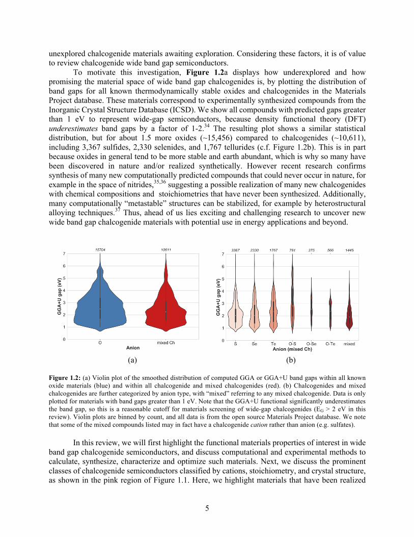
To motivate this investigation, Figure 1.2a displays how underexplored and how promising the material space of wide band gap chalcogenides is, by plotting the distribution of band gaps for all known thermodynamically stable oxides and chalcogenides in the Materials Project database. These materials correspond to experimentally synthesized compounds from the Inorganic Crystal Structure Database (ICSD). We show all compounds with predicted gaps greater than 1 eV to represent wide-gap semiconductors, because density functional theory (DFT) underestimates band gaps by a factor of 1-2.34 The resulting plot shows a similar statistical distribution, but for about 1.5 more oxides (~15,456) compared to chalcogenides (~10,611), including 3,367 sulfides, 2,330 selenides, and 1,767 tellurides (c.f. Figure 1.2b). This is in part because oxides in general tend to be more stable and earth abundant, which is why so many have been discovered in nature and/or realized synthetically. However recent research confirms synthesis of many new computationally predicted compounds that could never occur in nature, for example in the space of nitrides,35,36 suggesting a possible realization of many new chalcogenides with chemical compositions and stoichiometries that have never been synthesized. Additionally, many computationally “metastable” structures can be stabilized, for example by heterostructural alloying techniques.37 Thus, ahead of us lies exciting and challenging research to uncover new wide band gap chalcogenide materials with potential use in energy applications and beyond.
(a) (b)
Figure 1.2: (a) Violin plot of the smoothed distribution of computed GGA or GGA+U band gaps within all known oxide materials (blue) and within all chalcogenide and mixed chalcogenides (red). (b) Chalcogenides and mixed chalcogenides are further categorized by anion type, with “mixed” referring to any mixed chalcogenide. Data is only plotted for materials with band gaps greater than 1 eV. Note that the GGA+U functional significantly underestimates the band gap, so this is a reasonable cutoff for materials screening of wide-gap chalcogenides (EG > 2 eV in this review). Violin plots are binned by count, and all data is from the open source Materials Project database. We note that some of the mixed compounds listed may in fact have a chalcogenide cation rather than anion (e.g. sulfates). In this review, we will first highlight the functional materials properties of interest in wide band gap chalcogenide semiconductors, and discuss computational and experimental methods to calculate, synthesize, characterize and optimize such materials. Next, we discuss the prominent classes of chalcogenide semiconductors classified by cations, stoichiometry, and crystal structure, as shown in the pink region of Figure 1.1. Here, we highlight materials that have been realized
6
experimentally, and identify promising theoretical predictions to inform and inspire continued research in this field. Lastly, we summarize the most prominent applications of wide gap chalcogenide semiconductors in electronic devices, and discuss new potential device architectures. Since there is no clear boundary between transparent and non-transparent, we define “wide band gap semiconductors” as semiconductors whose band-to-band absorption edge appears larger than 2 eV (wavelength less than 600 nm). We focus only on thin film, n- or p-type doped materials, and exclude highly insulating chalcogenides and amorphous chalcogenides from this review, referring the reader elsewhere.38,39 Due to the multidisciplinary nature of these materials, this review is intended for a wide audience, from computational scientists to experimental materials scientists to engineers focusing on particular optoelectronic technologies. Thus, we have tailored each section to be either read independently or together as a comprehensive review.
2.Methods The primary requirements of functional wide gap chalcogenide semiconductors we discuss in this text differ by application, but most share four basic requirements: (1) synthesizability and stability to thermal, chemical, and other conditions of interest, (2) a wide enough band gap to ensure transparency to light of particular wavelength range, (3) high enough mobility to ensure opto-electronic device integration, (4) n- or p-dopability to ensure a sufficient concentration of electric charge carriers. Here, we discuss both the theoretical and experimental considerations of each of these properties, which are pertinent to designing high performance wide gap chalcogenide materials. We will focus on properties of interest for wide band gap semiconductors for photovoltaics and transparent electronics, since they are desirable and rare, though we also mention properties important in other applications such as photocathodes for solar water splitting and light emitting diodes (LEDs). Throughout this section, we also provide evidence why chalcogenides in particular could be an important, underexplored chemical space to look for materials with these properties, as well as highlight some unique challenges of chalcogenide materials.
Up until recently, material candidates were selected for synthesis based primarily on chemical intuition and theoretical approximations. Historically, it was easier to grow materials and measure their conductivities and transparencies than to perform expensive ab initio computation to assess such properties. Recent advances in high performance computing and the goals of Materials Genome Initiative (MGI) have driven development of computational platforms, such as the Materials Project,40 Aflowlib,41 NRELMatDB,42–44 and Open Quantum Materials Database45 that store information from ground state DFT calculations and allow facile exploration and screening of material candidates for desired properties. This accessibility of data has fundamentally changed how experimental materials scientists select candidate materials for synthesis.
Here, we review computational screening and experimental research methods related to wide band gap semiconductors. There are three primary computational approaches for such screenings. The first searches through computational materials property database, and applies a series of criteria to screen for descriptors of a desired structure or functionality. The second approach looks beyond the known materials reported in the International Crystal Structure Database (ICSD) to calculate novel, stable classes of compounds that have never been synthesized, and then screens within the new set for desired structure and functionality. The third, which is
7
gaining more prominence in the materials science community, applies machine learning algorithms to a particular subset of materials to predict entirely new composition, structures, and properties. In Section 3 we will discuss some key findings from ab initio computational screenings of wide-gap chalcogenides using the properties and descriptors discussed in 2.1.
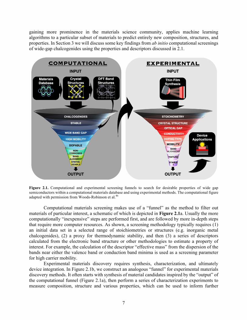
Figure 2.1. Computational and experimental screening funnels to search for desirable properties of wide gap semiconductors within a computational materials database and using experimental methods. The computational figure adapted with permission from Woods-Robinson et al.46
Computational materials screening makes use of a “funnel” as the method to filter out
materials of particular interest, a schematic of which is depicted in Figure 2.1a. Usually the more computationally “inexpensive” steps are performed first, and are followed by more in-depth steps that require more computer resources. As shown, a screening methodology typically requires (1) an initial data set in a selected range of stoichiometries or structures (e.g. inorganic metal chalcogenides), (2) a proxy for thermodynamic stability, and then (3) a series of descriptors calculated from the electronic band structure or other methodologies to estimate a property of interest. For example, the calculation of the descriptor “effective mass” from the dispersion of the bands near either the valence band or conduction band minima is used as a screening parameter for high carrier mobility.
Experimental materials discovery requires synthesis, characterization, and ultimately device integration. In Figure 2.1b, we construct an analogous “funnel” for experimental materials discovery methods. It often starts with synthesis of material candidates inspired by the “output” of the computational funnel (Figure 2.1a), then perform a series of characterization experiments to measure composition, structure and various properties, which can be used to inform further
8
synthesis experiments. Ultimately the goal often is to incorporate the synthesized and characterized material into a device stack. We will discuss each of these rungs of the computational and experimental funnels next, and consider possible device applications in the last section of this review. 2.1SynthesizabilityandStability.
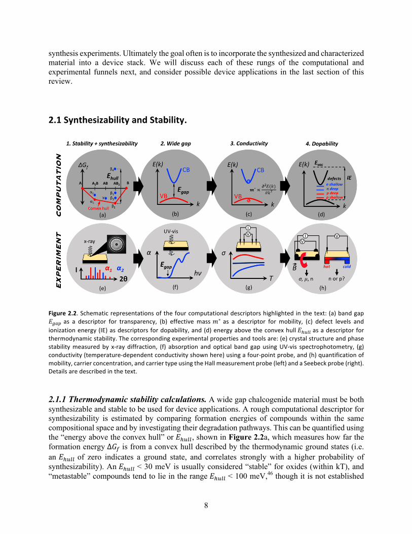
Figure2.2.Schematicrepresentationsofthefourcomputationaldescriptorshighlightedinthetext:(a)bandgap𝐸"#$ as a descriptor for transparency, (b) effective mass𝑚∗ as a descriptor for mobility, (c) defect levels andionizationenergy(IE)asdescriptorsfordopability,and(d)energyabovetheconvexhull𝐸'())asadescriptorforthermodynamicstability.Thecorrespondingexperimentalpropertiesandtoolsare:(e)crystalstructureandphasestabilitymeasured by x-ray diffraction, (f) absorption andoptical band gap usingUV-vis spectrophotometry, (g)conductivity(temperature-dependentconductivityshownhere)usingafour-pointprobe,and(h)quantificationofmobility,carrierconcentration,andcarriertypeusingtheHallmeasurementprobe(left)andaSeebeckprobe(right).Detailsaredescribedinthetext. 2.1.1 Thermodynamic stability calculations. A wide gap chalcogenide material must be both synthesizable and stable to be used for device applications. A rough computational descriptor for synthesizability is estimated by comparing formation energies of compounds within the same compositional space and by investigating their degradation pathways. This can be quantified using the “energy above the convex hull” or 𝐸'()), shown in Figure 2.2a, which measures how far the formation energy ∆𝐺, is from a convex hull described by the thermodynamic ground states (i.e. an 𝐸'()) of zero indicates a ground state, and correlates strongly with a higher probability of synthesizability). An 𝐸'()) < 30 meV is usually considered “stable” for oxides (within kT), and “metastable” compounds tend to lie in the range 𝐸'()) < 100 meV,46 though it is not established
9
whether chalcogenides conform to this limit.47 An upper 𝐸'()) limit of synthesizability has recently been proposed by the introduction of an amorphous “synthesizability skyline”, and the skyline of chalcogenides was found to be significantly higher than that of oxides.48 This suggests that thermodynamically metastable polymorphs may more achievable for chalcogenides than for oxides, which is a significant advantage for the number of possible materials that can be studied. The convex hull (𝐸'())) assessment can be applied early in a screening because it is usually computationally inexpensive. It does not require band structure calculations, only a DFT structure relaxation and cross comparison to other structures within a database. However, assessing stability and synthesizability by thermodynamics alone does not tell the full story. One issue chalcogenides face more than oxides is their stability in air and aqueous environments. Sulfides and selenides in general are more likely to oxidize and decompose under standard conditions than oxides, due to low energy reaction pathways with water or water vapor to form H2S or H2Se, though this is not universally true and can be studied computationally for particular compounds of interest. For example, screenings for photoelectrochemical materials have used calculations of Pourbaix diagrams to assess the stability of a compound.49 Additionally, p-type dopants must be stable within a host compound. For example, there have been several attempts of doping ZnO p-type with N and In/Ni, but these materials have later been shown to be unstable over time due to compensating donor defects.50,51 It is also important to note that computationally promising “synthesizable” and “stable” materials still may not be possible to achieve in practice due to competing reactions, various decomposition pathways, degassing, or uncertainties in calculations, among other reasons. 2.1.2 Experimental synthesis and phase purity. One of the best ways to determine synthesizability and stability of a given material system is to synthesize it, but this is not necessarily straightforward. There is a huge variety of bulk and thin film growth techniques and numerous interconnected parameters to optimize in synthesis and post-processing, as covered in many texts.52–56 Wide band gap semiconductors can be made in forms of bulk, thin film, 2D, or even quantum dots. Thin films are usually the most useful form for electronic device applications. Thin film transparent chalcogenides have been synthesized by (1) physical vapor deposition (PVD),57 including sputtering,58 pulsed laser deposition (PLD),59 and thermal or electron-beam evaporation,60,61 molecular beam epitaxy (MBE),62,63 by (2) chemical vapor deposition, usually involving some reactions between precursors, such as atomic layer deposition (ALD),64,65 metal organic chemical vapor deposition (MOCVD)66 and plasma-enhanced chemical vapor deposition (PECVD),67 or by (3) solution processes, including spray pyrolysis,68 sol-gel,69,70 and chemical bath deposition.71 Post-deposition treatments can be applied to enhance crystallinity or introduce dopants, such as exposure to gas (e.g. sulfurization and selenization, common in chalcopyrite materials)72 and rapid thermal annealing,73 and films can be doped via ion implantation or diffusion. Synthesis methods for bulk semiconductors varies, spanning a wide range of material quality, including solidstatereaction,sparkplasmasintering11,floatingzonesynthesis,74growthfrommelttechniquese.g.CzochralskiandBridgmangrowth,75,76etc.To achieve semiconducting materials in layer-controlled 2D forms, the two major directions are top-down methods, i.e. exfoliating materials from their bulk counterparts, and bottom-up methods, i.e. direct synthesis of 2D materials from constituent elements or precursors.77 After synthesis, stoichiometry and elemental uniformity can be determined by x-ray fluorescence (XRF), Rutherford backscattering spectroscopy (RBS), x-ray photoelectron spectroscopy (XPS, limited to surface stoichiometry),
10
energy dispersive x-ray spectroscopy (EDS or EDX), among other techniques. Sometimes off-stoichiometric synthesis is useful for achieving targeting properties and high conductivity. Achieving the right stoichiometry of chemical elements does not guarantee that a crystal phase of interest has been made. Many of the low temperature growth techniques result in amorphous or nanocrystalline material, which has to be treated for crystallization. X-ray diffraction techniques are often used to confirm whether a targeted crystal phase has been synthesized.78 Measured diffraction peaks can be compared to standard reference patterns, which can be experimental for known materials or generated from a computed crystal structure for new materials. Secondary phases may be present, but not visible with diffraction. Sometimes nanocrystalline phases can be detected by electron diffraction or Raman spectroscopy, among other methods, but Raman reference patterns are not as easily accessible. A schematic of XRD experiments is shown in Figure 2.2e. Additional constraints exist when synthesizing chalcogenide materials for device applications, as discussed earlier. Most importantly, materials need to be stable in air and at the interface of relevant chemicals they are grown upon or below in a device stack, or exposed to during their lifecycle. To this end, it is useful to measure material properties after exposure in the air for some time. Additional constraints include temperature stability (most devices have a “thermal budget”), stability to UV irradiation (for devices that will be in the sun), Pourbaix stability (e.g. in PEC device applications, where materials are often exposed to extremely acidic or basic conditions), etc. It is also important to consider the lifetime of the device when designing materials to be incorporated, i.e. whether migration of dopants or segregation into secondary phases will occur over time. End-of-life decomposition and recyclability of materials is also becoming increasingly important in rational materials design, as researchers strive to implement principles of circular economy.79 2.2Bandgap. 2.2.1 Computational optical properties. A material with a band gap EG higher than approximately 3.1 eV (corresponding to a band absorption onset at 400 nm), is typically considered “transparent” so long as other effects are negligible (e.g. free carrier absorption and defect absorption; c.f. below). In this review we’ll also be discussing semi-transparent materials with band gaps greater than 2 eV (band absorption onset at 620 nm), hence the term “wide band gap semiconductors.” Band gap and dominant band-to-band absorption can be estimated from electronic structure calculations from ground state density functional theory (DFT), as shown schematically in Figure 2.2b as the lowest energy difference between the conduction band minimum (CBM) and the valence band maximum (VBM). Different DFT functionals trade off band gap accuracy for computational efficiency. Fast, “cheap” DFT calculations such as GGA+U have been calculated and tabulated for nearly all experimentally known materials in computational databases (tens of thousands), but have been shown to significantly underestimate band gaps. More expensive calculations such as hybrid functional HSE06 and GW can also be applied in a high-throughput manner, albeit at a greater computational cost. These computational methods have been benchmarked to predict band gaps on a case-by-case basis within 25% uncertainty,80 and are available in limited quantities (~1000) in some computational databases (e.g. materials.nrel.gov).
11
In general oxides tend to exhibit a wider gap than counterpart chalcogenides, but as shown in Figure 1.2 there are still many chalcogenides with wide gaps. We note that a wide band gap alone does not necessarily guarantee optical transparency. Dominant transitions tend to occur at direct gaps, rather than indirect gaps that require phonon assistance for absorption. At high carrier dopings, intraband scattering and free carrier absorption can cause loss of transparency within the near-infrared and visible spectrum that increases with doping concentration. Additionally, intrinsic defects and intentionally introduced dopants can introduce defect levels within the gap that reduce optical transparency, and in some inorganic materials excitonic absorption may also become significant.81 2.2.2 Experimental optical properties. Optical properties of experimental interest to wide gap chalcogenide thin film semiconductors include transmittance, reflectance, and absorption. These properties are typically measured for thin films with UV-Vis-IR spectrophotometry as a function of wavelength, as depicted in Figure 2.2f. Transmittance and reflectance measurements can be used to calculate the absorption coefficient, a = − ln 1
234/𝑑, as a function of wavelength. From
the absorption spectrum, the low-frequency cutoff is typically fit to estimate the band gap using the Tauc relation ahν 2/9, where r = 1/2 is assumed for allowed direct transitions and r = 2 is assumed for allowed indirect transitions. However, such fits are often ambiguous depending on the selected energy range. Thus, it is usually impossible to use this method to experimentally determine whether the studied material has a direct or indirect band gap, yet many literature reports including those in this review do so nonetheless. Band-to-band transitions typically occur in semiconductors for absorption coefficients of approximately 104 cm-1, so the cutoff is usually drawn around this value as an alternative method to estimate the optical absorption threshold without claiming the band gap. Spectrophotometers can be equipped with an integrating sphere to measure diffuse reflectance for rough samples. Other useful optical characterization techniques include Fourier transform infrared spectroscopy (FTIR) to probe the infrared, and ellipsometry to extract optical constants (i.e. refractive index n and extinction coefficient k), and there are many in-depth reviews and textbooks on these methods.82–84
Despite the prevalence of these characterization methods, there is some discrepancy within the literature surrounding how exactly such values are reported. As mentioned above, the exact energy range for Tauc plots is not standardized and depends on the discretion of the researcher. In particular, it can be very difficult to conclusively determine from Tauc plots whether material has direct or indirect band gap, and to accurately estimate indirect band gap for which the optical transition probability is usually low. In addition, researchers should be aware that transmittance and reflectance are thickness dependent measurements, leading to different accessible dynamic range of absorption coefficient measurements. Thus, it is important to keep these factors in mind when claiming Tauc-derived experimental band gaps and comparing reported values for samples with very different thicknesses.
To illustrate some of these discrepancies, Figure 2.3 shows the optical properties of sputtered zinc-blende ZnSe thin films, plotted as a function of film thickness. As evidences from Figure 2.3a and b, transmittance values are a function of wavelength and are heavily influenced by Fabry-Perot interference fringes related to scattering of light from the front and back of the film. Thus it is ambiguous to report transmittance from a single wavelength number, yet this is still done routinely in the literature. One way to solve this issue is to use the reflectance corrected transmittance, 𝑇?@AA =
B23C
, as shown in Figure 2.3c. For a given thickness, this mathematical

12
transformation results in a monotonically increasing Tcorr with wavelength, and thus a more reliable value. However, even 𝑇?@AA still depends somewhat on film thickness (Figure 2.3c), so one can always expect a “transparent” thin film if it is thin enough. Considering these two factors, transmittance can be useful as a reference but is not an appropriate metric to compare various materials systems. Instead, the it is recommended to report the absorption coefficient, defined as a=-ln(Tcorr))/d, to avoid thickness and wavelength dependence. Figure 2.3d shows the absorption coefficients as a function of wavelength and thickness. In this case there is a fixed onset at ~490 nm where absorption reaches 104 cm-1 regardless of thickness, so we can interpret this value as a band gap of approximately 2.5 eV (compare to the literature reported gap of 2.7 eV).120 We note that ZnSe is a direct band gap semiconductor so the measured 2.5 eV optical absorption onset is within a range of uncertainty of reported 2.7 eV band gap, but in indirect semiconductors it may be less obvious. In this review, we will focus on reporting optical band gap because it is the standard value reported consistently in the literature, yet we will often use the “~” symbol to emphasize aforementioned experimental and analytical uncertainties. We also provide references that report absorption coefficient, transmittance, and other optical properties.
Figure 2.3. Optical properties of sputtered ZnSe thin films as a function of thickness. (a) Transmittance; (b) Reflectance; (c) Reflectance-corrected transmittance; (d) Absorption coefficient, indicating how optical band gap EG is estimated. 2.3MobilityandConductivity. The carrier mobility 𝜇 of a material is set by the intrinsic dispersion of the electronic bands as quantified by effective mass 𝑚∗, and is limited by the mean free path of carriers with charge q (or the inverse of mean free path, scattering time 𝜏), such that:
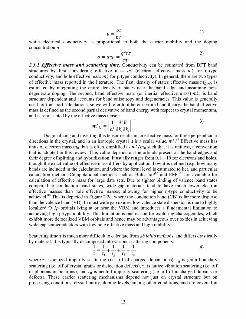
13
𝜇 =𝑞𝜏𝑚∗
1)
while electrical conductivity is proportional to both the carrier mobility and the doping concentration 𝑛:
𝜎 = 𝑞𝑛𝜇 =𝑞I𝑛𝜏𝑚∗
2)
2.3.1 Effective mass and scattering time. Conductivity can be estimated from DFT band structures by first considering effective mass 𝑚∗ (electron effective mass 𝑚J
∗ for n-type conductivity, and hole effective mass 𝑚'
∗ for p-type conductivity). In general, there are two types of effective mass reported in the literature. The first, density of states effective mass 𝑚KLM
∗ , is estimated by integrating the entire density of states near the band edge and assuming non-degenerate doping. The second, band effective mass (or inertial effective mass) 𝑚N
∗ , is band structure dependent and accounts for band anisotropy and degeneracies. This value is generally used for transport calculations, so we will refer to it herein. From band theory, the band effective mass is defined as the second partial derivative of band energy with respect to crystal momentum, and is represented by the effective mass tensor:
𝒎∗PQ =
1ℎI
𝜕I𝑬𝜕𝑘P𝜕𝑘Q
32
3)
Diagonalizing and inverting this tensor results in an effective mass for three perpendicular directions in the crystal, and in an isotropic crystal it is a scalar value, 𝑚∗.85 Effective mass has units of electron mass 𝑚V, but is often simplified as 𝑚∗/𝑚V such that it is unitless, a convention that is adopted in this review. This value depends on the orbitals present at the band edges and their degree of splitting and hybridization. It usually ranges from 0.1 – 10 for electrons and holes, though the exact value of effective mass differs by application, how it is defined (e.g. how many bands are included in the calculation, and where the fermi level is estimated to lie), and particular calculation method. Computational methods such as BoltzTraP86 and EMC87 are available for calculation of effective mass for large data sets. Due to tighter binding of valence band states compared to conduction band states, wide-gap materials tend to have much lower electron effective masses than hole effective masses, allowing for higher n-type conductivity to be achieved.88 This is depicted in Figure 2.2c, where the conduction band (CB) is far more disperse than the valence band (VB). In most wide gap oxides, low valence state dispersion is due to highly localized O 2p orbitals lying at or near the VBM and introduces a fundamental limitation to achieving high p-type mobility. This limitation is one reason for exploring chalcogenides, which exhibit more delocalized VBM orbitals and hence may be advantageous over oxides in achieving wide gap semiconductors with low hole effective mass and high mobility. Scattering time 𝜏 is much more difficult to calculate from ab initio methods, and differs drastically by material. It is typically decomposed into various scattering components:
1𝜏 =
1𝜏P+1𝜏"+1𝜏)+1𝜏X
4)
where 𝜏P is ionized impurity scattering (i.e. off of charged dopant ions), 𝜏" is grain boundary scattering (i.e. off of crystal grains or dislocation defects), 𝜏) is lattice vibration scattering (i.e. off of phonons or polarons), and 𝜏X is neutral impurity scattering (i.e. off of uncharged dopants or defects). These carrier scattering mechanisms depend not just on crystal structure but on processing conditions, crystal purity, doping levels, among other conditions, and are covered in
14
detail elsewhere.89–91 When transparent semiconductors are degenerately doped to concentrations approximately >1020 cm-3, it is typical for temperature-independent ionized impurity scattering to dominate.92,93 Most computational screening studies assume ionized impurity scattering dominates in wide gap chalcogenides such that the constant relaxation time approximation (cRTA) holds. However computational methods and associated software, such as aMoBT, to consider other scattering effects in the calculation of mobility are advancing.94 We note that the thresholds for “high” mobility and conductivity are arbitrary, and requirements will be different depending on the particular application. 2.3.2 Mobility and Conductivity Measurements. Figure 2.2g and Figure 2.2h demonstrate the two most common ways to measure electrical conductivity in thin film materials. In the first configuration in Figure 2.2g, a four-point probe is used to measure sheet resistance of bulk or thin film semiconductors, and in-plane conductivity can be calculated if film thickness known. The basic concept is to source current through two terminals while generating and measuring voltage from the other two terminals. Vertical, or out-of-plane resistivity can be measured by preparing a sandwich structure with conductive materials as top/bottom electrodes and target material in the middle, and measuring its electrical resistance, also requiring independent thickness measurements to extract electrical conductivity. Hall effect measurements shown on the left of Figure 2.2h are often used to obtain Hall mobilities and carrier concentrations (as well as carrier type). When a source current flows through two terminals, carriers deviate under a vertical magnetic field and accumulate at the edges, generating a Hall voltage proportional to carrier concentrations. Mobility can then be back-calculated from conductivity and carrier concentrations, and carrier type is indicated from the sign of the Hall voltage. The measured mobility typically consists of multiple scattering mechanisms, and 𝜏 can be back-calculated using Equation 1 if the effective mass is known. To reveal the particular scattering mechanism for a thin film, the Hall mobility can be measured as a function of temperature. For example, a temperature-dependent mobility suggests phonon scattering, whereas temperature independent mobility is usually indicative that ionized impurity scattering dominates. This latter case is a typical dominant scattering mechanism in highly conductive n-type transparent conducting oxides, and is also present in several transparent conducting sulfides. Conductivity can also be measured optically, using light to excite free carriers. This is particularly useful to evaluate intra-grain mobility, and for bulk powder samples which cannot be analyzed with four-point probe or Hall setups due to their granularity. This method relies on the optical absorption at photon energies below the energy gap, which is related to the free electrons or holes. The relationship is summarized by Drude theory, from which conductivity, mobility, carrier concentration can be calculated if effective mass is known.95 2.4Dopability In addition to low 𝑚∗ and high 𝜏, Equation 1 illustrates that high conductivity also requires a sufficiently high carrier concentration 𝑛 for electrons (or p for holes). This depends on the material’s dopability, which is a function of several parameters. For example, to be a highly conductive wide gap p-type semiconductor, a material must support the introduction of p-type dopants (i.e. dopant must be soluble and energetically stable), be dopable to a high enough concentration, and not be susceptible to compensation by n-type “hole killer” defects. It has been

15
theorized that n-type dopability is favorable in materials with large electron affinities, while p-type dopability is favorable in materials with small ionization energies.33 This is one reason why it is more difficult to dope wide gap materials; in general as the gap increases, the CB shifts towards vacuum level and the VB shifts away from it. Additionally, the wider the gap the more likely defect levels are to emerge within the gap and induce carrier compensation. Because of 3p, 4p, or 5p character of chalcogen atoms, valence levels of chalcogenides tend to lie closer to vacuum than oxides with 2p character of oxygen atoms, suggestive of a higher propensity for p-type doping in chalcogenides compared to oxides. However, while noting this general trend, many chalcogenides are in fact highly n-type dopable as well, and defect calculations are usually necessary to understand dopability. 2.4.1 Computational dopability.
Understanding carrier compensation by defects and selecting appropriate dopants, requires defect formation energy calculations, which use DFT supercell calculations and thus are computationally quite expensive. These calculations can estimate the energy level of particular dopants, whether they are shallow or deep, and whether they should lead to n-type or p-type conductivity (c.f. Figure 3.3). The defect formation energy, 𝐸,[𝑋[], is the energy cost to create or remove an isolated defect 𝑋 with charge state 𝑞 from a bulk material and describes how favorable various defects and dopants are to form compared to one another. It is calculated as:
𝐸, 𝑋[ = 𝐸]@] 𝑋[ − 𝐸]@] 𝑏𝑢𝑙𝑘 − 𝑛P𝜇PP
+ 𝑞𝐸a + 𝐸?@AA (5)
where 𝐸]@] 𝑋[ and 𝐸]@] 𝑏𝑢𝑙𝑘 are DFT formation energies of defective and bulk supercells, − 𝑛P𝜇PP is the summation over chemical potentials of the defect elements, 𝑞𝐸a is the cost in energy of adding or removing an electron, and 𝐸?@AA are correction term(s) that account for mirroring of charges, VBM alignment, and other spurious computational effects. The calculated formation energies can be used as inputs to thermodynamic simulations that output equilibrium defect concentration, carrier densities, and Fermi level positions for an assumed set of chemical potentials. Specifics of these defect calculations and thermodynamic simulations are covered in many comprehensive reviews.96,97 Recently, codes such as PyCDT and Pylada have been developed to run defect calculations on a high throughput framework, making them more accessible to the research community.98,99 Defect calculations can also be used to be screened for various types of defect tolerance100,101 and for deep-level defect induced absorption that would decrease optical transparency.102
To roughly estimate dopability, some high throughput studies have calculated the branch point energy (BPE, i.e. Fermi level stabilization energy), which approximates the position where the Fermi level is pinned when defects are introduced.103 The BPE is calculated using the following formula:104
Ecd =12𝑁f
1𝑁gh
𝜖ghjk
lmn
P
+1𝑁oh
𝜖ohjk
lpn
Pf
(6)
where 𝑁f is the number of k-points in the DFT calculation, 𝑁gh and 𝑁oh the number of CBs and VBs averaged over, and 𝜖ghjk and 𝜖ohjk the DFT energy eigenvalues at each k-point. This descriptor is advantageous because it uses only bulk DFT band structure calculations and can be
16
simply incorporated into to high throughput methodologies. BPE has been benchmarked for several binary wurtzite, zincblende and rocksalt systems,104 and has been used in screenings for p-type transparent conductors.105,106 However, despite its advantages BPE does not indicate whether a semiconductor is actually dopable in practice, cannot explain deep defect levels, varies depending on how many bands are averaged over, and has not yet been benchmarked for a comprehensive set of structures and chemistries.107 2.4.2. Experimentally quantifying doping.
Dopants are introduced intrinsically or intentionally during growth, or by a subsequent processing step such as rapid thermal processing or ion implantation. At concentrations greater than approximately 1%, impurity concentration can usually be determined via x-ray fluorescence spectroscopy (XRF), x-ray fluorescence spectroscopy (XPS), energy dispersive spectroscopy (EDS), or Rutherford Backscattering spectroscopy (RBS), among other methods. Some highly sensitive techniques such as Secondary-Ion mass spectrometry (SIMS) can detect impurities down to parts per million or even parts per billion,108,109 but their quantification requires reference samples. X-ray absorption spectroscopy (XAS) can be useful to determine the location and coordination of defects, i.e. whether they are vacancies VA, interstitials Ai, substitutions BA, but also requires standards or complementary modeling. We note that the transparent semiconductor and other communities sometimes use the term “dopant” for incorporation of chemical substitutions of greater than 1%, even in solid solutions or systems where phase segregation occurs, so it is important to be clear about diversity of this terminology.
Dopant concentration does not always translate to carrier concentration, so it is essential to measure carrier concentration directly. In the context of this article, the goal of doping a semiconductor is to increase the majority carrier concentration without significantly reducing the mobility. These two properties can be measured using a Hall effect, as described previously and schematically shown in Figure 2.2h (left). It is highly recommended to ensure that the measured carrier type is the same and the carrier density is similar upon the magnetic field reversal. Even with these precautions, it may be difficult to accurately determine whether a material is doped n-type or p-type from Hall effect measurements of low-mobility materials or magnetic compounds. In such cases it is possible to measure the Seebeck coefficient (i.e. thermopower) using a Seebeck probe (Figure 2.2h, right), which is less sensitive to experimental artifacts. The majority carrier type is indicated by the sign of Seebeck coefficient, and the carrier concentration is often inversely proportional to the magnitude of Seebeck coefficient. 2.5 Band positions, alignments, and other properties. Additional criteria essential for the implementation of materials into electronic device applications is the positions of band edges and of the Fermi level (i.e. ionization energy, electron affinity, and work function). These positions referenced to those of the other layers in a particular device, and the band bending of the resulting interface or junction, dictate the dynamics of electron or hole transport through the interface of the device. For example, in order to align a top contact n-type wide-gap material to a p-type CdTe solar cell, the position of the conduction band of the n-type material must be similar to the conduction band position of CdTe.110 As mentioned in 2.1.3, chalcogenide materials tend to have higher VBMs closer to vacuum (lower ionization energy) than their oxide counterparts. This could enable band alignment configurations in devices and junctions
17
that are not possible in oxides. Other properties of interest to wide band gap semiconductor materials and their practical applications include flexibility, lattice matching (i.e. interatomic distance), microstructure, among other features.
2.5.1 Computational band alignment As depicted in the bottom of the computation funnel of Figure 2.1, band alignment can be
qualitatively assessed using DFT surface calculations of alternating crystal and vacuum slabs to estimate the valence levels with respect to vacuum, reviewed comprehensively elsewhere.111,112 Some studies have used these calculations for high throughput screenings, in particular in searches for electrochemical catalysts and electrodes.49 Band alignments can differ drastically depending on the surface morphology, including crystallographic plane, surface termination and defects. As a result, band alignments in polycrystalline materials can be averaged over the most stable surfaces, but there is not yet a consensus amongst the DFT community about their treatment.113 In addition, band alignments are often modified in practice when two materials are brought into direct contact (rather than contact with vacuum). Such interfacial band alignment can be accessed from explicit interface slab calculations for any material pair for which the crystallographic relationship at the interface is well defined. This is difficult to do for most of the materials without considering interfacial defects or strain, hence such calculations are usually performed for epitaxial lattice-matched interfaces.
2.5.2 Experimental band alignment Experimentally, work functions (Fermi level with respect to vacuum level) are typically
measured by Kelvin probe or by UPS from secondary electron cutoff.114 Another powerful technique is XPS, which can be used to measure valence band alignments and band bending by following the shifts in the core levels. Such interface band alignment measurement experiments can be performed by bottom-up (layer by layer deposition) or top-down (depth profiling) modes, to experimentally measure band bending at interfaces, which is of particular importance to device applications (e.g. literature reports in Figure 4.6). The latter mode is more common in literature but less accurate due to chemical modification of the interface by sputtering with Ar ions. Complementary to XPS/UPS, Auger measurements are another possible way to detect the energy difference between the Fermi level and the valence band maximum.
3.Materials In this section, we highlight the major advances in various classes of dopable wide band gap chalcogenide semiconducting materials (EG > 2.0 eV), and compare their properties and their underlying physics. We will discuss bulk structures, intrinsic and extrinsic dopants, focusing mostly on materials that have been synthesized as polycrystalline thin films, and mentioning some alloys and composites. Experimental band gaps and electrical properties discussed are measured at approximately 300 K, unless otherwise denoted. We also highlight some of the binary chalcogenides, ternary chalcogenides, and oxychalcogenides that have been predicted via high throughput computational screening methods. Many of these materials have not yet been explored in-depth experimentally, so their calculations open up areas of future experimental research. As
18
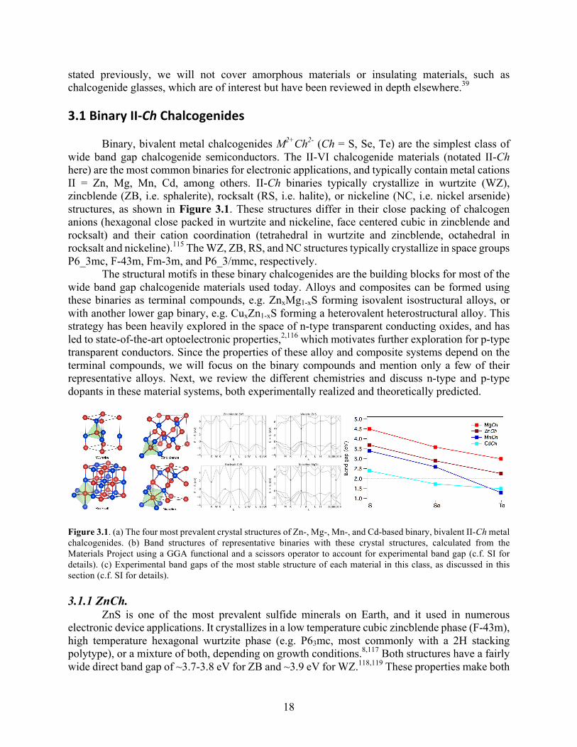
stated previously, we will not cover amorphous materials or insulating materials, such as chalcogenide glasses, which are of interest but have been reviewed in depth elsewhere.39 3.1BinaryII-ChChalcogenides Binary, bivalent metal chalcogenides M2+Ch2- (Ch = S, Se, Te) are the simplest class of wide band gap chalcogenide semiconductors. The II-VI chalcogenide materials (notated II-Ch here) are the most common binaries for electronic applications, and typically contain metal cations II = Zn, Mg, Mn, Cd, among others. II-Ch binaries typically crystallize in wurtzite (WZ), zincblende (ZB, i.e. sphalerite), rocksalt (RS, i.e. halite), or nickeline (NC, i.e. nickel arsenide) structures, as shown in Figure 3.1. These structures differ in their close packing of chalcogen anions (hexagonal close packed in wurtzite and nickeline, face centered cubic in zincblende and rocksalt) and their cation coordination (tetrahedral in wurtzite and zincblende, octahedral in rocksalt and nickeline).115 The WZ, ZB, RS, and NC structures typically crystallize in space groups P6_3mc, F-43m, Fm-3m, and P6_3/mmc, respectively.
The structural motifs in these binary chalcogenides are the building blocks for most of the wide band gap chalcogenide materials used today. Alloys and composites can be formed using these binaries as terminal compounds, e.g. ZnxMg1-xS forming isovalent isostructural alloys, or with another lower gap binary, e.g. CuxZn1-xS forming a heterovalent heterostructural alloy. This strategy has been heavily explored in the space of n-type transparent conducting oxides, and has led to state-of-the-art optoelectronic properties,2,116 which motivates further exploration for p-type transparent conductors. Since the properties of these alloy and composite systems depend on the terminal compounds, we will focus on the binary compounds and mention only a few of their representative alloys. Next, we review the different chemistries and discuss n-type and p-type dopants in these material systems, both experimentally realized and theoretically predicted.
Figure 3.1. (a) The four most prevalent crystal structures of Zn-, Mg-, Mn-, and Cd-based binary, bivalent II-Ch metal chalcogenides. (b) Band structures of representative binaries with these crystal structures, calculated from the Materials Project using a GGA functional and a scissors operator to account for experimental band gap (c.f. SI for details). (c) Experimental band gaps of the most stable structure of each material in this class, as discussed in this section (c.f. SI for details). 3.1.1 ZnCh.
ZnS is one of the most prevalent sulfide minerals on Earth, and it used in numerous electronic device applications. It crystallizes in a low temperature cubic zincblende phase (F-43m), high temperature hexagonal wurtzite phase (e.g. P63mc, most commonly with a 2H stacking polytype), or a mixture of both, depending on growth conditions.8,117 Both structures have a fairly wide direct band gap of ~3.7-3.8 eV for ZB and ~3.9 eV for WZ.118,119 These properties make both

19
structures suitable as buffer layers and, if sufficiently dopable, as transparent electrode layers in solar cells. Importantly, ZnS is an non-toxic, earth-abundant material that is closely lattice matched with Cu(InGa)Se2, the absorber layer in CIGS solar cells.120 ZnS is also important for its luminescence properties.
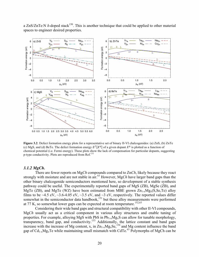
The conductivity of undoped ZnS is usually very low,121 likely due to low carrier concentration, and at slight off-stoichiometries is reported intrinsically n-type due to interstitial Zn (Zni), or S vacancies (VS). However, ZnS has been reported to be ambipolar extrinsically doped, e.g. n-type by AlZn (up to ~10-3 S cm-1)122 and p-type by CuZn (~10-5 S cm-1 for 0.1% Cu, and even up to ~1 S cm-1 for 9%, though this may be influenced by Cu-S impurities; c.f. “Alloys and composites” section) .123 Other known n-type dopants are FS (conductivities ~2 ×10⁻⁷ S cm-1),124 ClS,125 InZn,126 among others, and co-doping strategies have been employed as p-type dopants (e.g. N/Li,127 and In/Ag/N).126 This achievement of both n-type and p-type conductivity is supported by the low effective mass of both electrons and holes in ZnS, as evident from the highly dispersive band edges (c.f. Figure 3.1). The ambipolar dopability also reflects adequate band positions with respect to vacuum, with reported electron affinities in zincblende ZnS of approximately 3.8-4.0 eV and ionization energies ~7.5 eV by both computation and experiment (c.f. Section 4.3).128–130 Additionally, ZnS has minimal compensating defects, as demonstrated computationally in a recent defect screening study of binary chalcogenides.131 This study found p-type conductivity promising in doping Zn sites with Cu (CuZn), confirming experimental results, as well as Na (NaZn), K (KZn) and doping S sites with N (NS), as depicted in Figure 3.2a. This is evident by the low defect formation energy when the Fermi level is near the VBM.
Zincblende ZnSe has a lower band gap than zincblende ZnS (~2.7 eV at room temperature, ~2.8 eV at 10 K), but it is still sufficiently transparent for use as a window layer in solar cell applications.132,133 It is also intrinsically n-type due to Zni or VSe, though p-type conductivities up to ~5 S cm-1 have been demonstrated in metalorganic vapor phase epitaxy films.134 Various dopants have been explored experimentally to modify the conductivity of ZnSe, e.g. NSe (p-type, 0.06 S cm-1 and mobilities up to 86 S cm-1),135 GaZn (n-type, 20 S cm-1),136 ClS (n-type, ~333 S cm-
1),137 among others. ZnSe has an even lighter effective mass than ZnS. Particularly notable is that the mobility in high-quality, nominally updoped MBE-grown intrinsic n-type ZnSe has been reported up to 550 cm2
V-1 s-1 at room temperature and is dominated at room temperature by polar
optical phonon scattering. This high mobility motivates ZnSe’s application in devices such as light emitting diodes (LEDs) and thin film transistors (TFTs).138
ZnTe also crystallizes in its ground state in the zincblende structure, with a direct gap of ~2.3 eV,139 and its intrinsic p-type conductivity is reportedly to be due to VZn. P-type dopants NTe (25 S cm-1),140 CuZn (~0.33 S cm-1),141 and SbZn (~30 S cm-1)142 are used to improve the p-type conductivity of ZnTe, and several of these dopants have been confirmed computationally with defect studies (c.f. Figure 3.2b).131 N-type doping is trickier but has been achieved in epitaxial crystals with AlZn, ClTe, and SnZn.143–146 p-type ZnTe is commonly used in CdTe solar cells as a back contact due to its small valence band offset with CdTe of only <100 meV (c.f. Section 4)147, and has been explored for photocatalysis applications.148 As expected from ionicity trends of the chalcogen anions, ZnS and ZnSe have been shown to have a wider band gap but lower achievable doping levels than ZnTe. A “δ-doping” technique has been used to leverage the wide band gap of ZnS and easy dopability of ZnTe149. Highly conductive p-type ZnSe and ZnS films were achieved using molecular beam epitaxy (MBE) to insert heavily N-doped ZnTe layers between each layer ZnSe or ZnS layer. The hole concentration in a ZnSe/ZnTe:N δ-doped stack reaches 7×1018 cm-3, and a [Na-Nd] value reaches 5×1017cm−3 in
20
a ZnS/ZnTe:N δ-doped stack150. This is another technique that could be applied to other material spaces to engineer desired properties.
Figure 3.2. Defect formation energy plots for a representative set of binary II-VI chalcogenides: (a) ZnS, (b) ZnTe (c) MgS, and (d) BeTe. The defect formation energy 𝐸, 𝑋[ of a given dopant 𝑋[ is plotted as a function of chemical potential (i.e. Fermi energy). These plots show the lack of compensation for particular dopants, suggesting p-type conductivity. Plots are reproduced from Ref.131 3.1.2 MgCh.
There are fewer reports on MgCh compounds compared to ZnCh, likely because they react strongly with moisture and are not stable in air.63 However, MgCh have larger band gaps than the other binary chalcogenide semiconductors mentioned here, so development of a stable synthesis pathway could be useful. The experimentally reported band gaps of MgS (ZB), MgSe (ZB), and MgTe (ZB), and MgTe (WZ) have been estimated from MBE grown Zn1-xMgx(S,Se,Te) alloy films to be ~4.5 eV, ~3.6-4.05 eV, ~3.5 eV, and ~3 eV, respectively. The reported values differ somewhat in the semiconductor data handbook,151 but these alloy measurements were performed at 77 K, so somewhat lower gaps can be expected at room temperature.152,63
Considering their wide band gaps and structural compatibility with other II-VI compounds, MgCh usually act as a critical component in various alloy structures and enable tuning of properties. For example, alloying MgS with PbS in Pb1-xMgxS can allow for tunable morphology, transparency, band gap, and conductivity.153 Additionally, the lattice constant and band gaps increase with the increase of Mg content, x, in Zn1-xMgxSe,154 and Mg content influence the band gap of Cd1-xMgxTe while maintaining small mismatch with CdTe.63 Polymorphs of MgCh can be
21
stabilized when alloyed with other materials. Computational investigation has predicted rocksalt as the stable phase for MgS and MgSe, and nickeline phase was predicted for MgTe alloys.155 According to computational defect studies of rocksalt MgS (c.f. Fig 4.5c) and wurtzite MgTe, alkali substitutional acceptor dopants NaMg and KMg and anion substitutional dopant NCh should lead to p-type dopability. However, the doping ability of other MgCh-based alloys requires further investigation.131 3.1.3 MnCh. MnS thin films are wide-gap semiconductors can crystallize in the WZ (γ) structure with a gap of 3.88 eV,156 in the ZB (β) structure with a gap of 3.8 eV in single crystal samples,157 rocksalt (α) with a gap of 2.8-3.2 eV and single crystal mobility of 10 cm2
V-1 s-1 (the most stable
phase at ambient conditions),151 as mixed-phase rocksalt and wurtzite with a gap of 3.0 eV,158 and as amorphous semiconductors with a gap of 2.8-3.0 eV.159 MnS is intrinsically p-type, likely due to doubly-ionized V--
Mn,160 with a low room temperature reported conductivity of ~10-5 S cm-1,161 and MnS has been doped by e.g. Cd.162 Generally, MnSe is stable in its rocksalt (α) structure163 and has a band gap of approximately 2.5 eV.164 Its zinc blende and wurtzite polymorphs have also been synthesized, with gaps of ~3.4 eV and 3.5-3.8 eV,165,166 respectively, and are of interest due to their structural compatibility with other III-V, II-VI semiconductor systems.166 MnSe has been synthesized in a high pressure in a nickeline phase as well. Doping has not been explored, but it is likely also p-type due to V--
Mn. MnTe usually crystallizes as nickeline phase as a ground state structure, while the band gap of zincblende polymorph of MnTe can reach 3.2 eV167. Nickeline MnTe has high p-type conductivity compared to the other Mn-based compounds, up to 5-6 S cm-
1, with Hall mobilities up to 0.5 cm2 V-1
s-1, room temperature intrinsic degenerate doping of 5x1019 cm-3 and an estimated hole effective mass of 1.5m0,37 but a lower band gap of 1.3 eV. WZ MnTe with a wider band gap of 2.7 eV can be stabilized by alloying with ZnTe,37 or by growth on InZnOx coated glass.168 The wide reported range of band gaps and conductivities within the MnCh system inspires further investigation into polymorphs with tunable properties. 3.1.4 CdCh. CdS is one of the most intensively investigated wide gap semiconductors, used in a large variety of optoelectronic applications, and has been heavily reviewed.169–171 This material is the archetype n-type buffer layer used commercially in CdTe and CIGS solar cells, 171,172and has been used for LEDs, TFTs, photonic/lasing devices, piezoelectrics. CdS most common form is hexagonal WZ, ZB phases have also been investigated, and there exists a high-pressure RS phase. Epitaxial growth has produced single phase, single crystal wurtzite material to quantify the room temperature direct gap at 2.5 eV (measured with ellipsometry), and the cubic phase has a similar but somewhat lower measured direct gap of approximately 2.4 eV. The RS phase has been reported to have an indirect gap of ~1.5-1.7 eV, consistent with band structure calculations.173 Polycrystalline thin films can be prepared by sputtering, CBD and thermal evaporation, among others, and tend to have a mixed WZ and ZB structure with room temperature band gaps of approximately 2.3-2.5 eV. This variation has been explained by the range of substoichiometric sulfur content in reported films due to various deposition temperatures.174,175 WZ CdS is typically grown n-type, and is ambipolar with nearly intrinsic electron conductivity of 2.8 x 10⁻² S cm-1 and nearly intrinsic hole conductivity of 1.5x10⁻² S cm-1.151
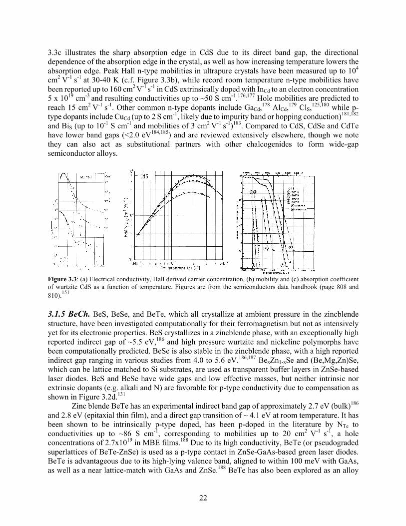
The temperature dependence of conductivity, electron concentration, and electron mobility in ultrapure CdS samples is shown in Figure 3.3. Hall measurements (c.f. Section 2.3 and 2.4) of carrier concentration and conductivity generally increase as temperature increases (Figure 3.3a), while mobility decreases with increased temperature due to carrier scattering (Figure 3.3b). Figure
22
3.3c illustrates the sharp absorption edge in CdS due to its direct band gap, the directional dependence of the absorption edge in the crystal, as well as how increasing temperature lowers the absorption edge. Peak Hall n-type mobilities in ultrapure crystals have been measured up to 104 cm2
V-1 s-1 at 30-40 K (c.f. Figure 3.3b), while record room temperature n-type mobilities have
been reported up to 160 cm2 V-1
s-1 in CdS extrinsically doped with InCd to an electron concentration 5 x 1019 cm-3 and resulting conductivities up to ~50 S cm-1.176,177 Hole mobilities are predicted to reach 15 cm2
V-1 s-1. Other common n-type dopants include GaCd,178 AlCd,179 ClS,125,180 while p-
type dopants include CuCd (up to 2 S cm-1, likely due to impurity band or hopping conduction)181,182 and BiS (up to 10-1 S cm-1 and mobilities of 3 cm2
V-1 s-1)183. Compared to CdS, CdSe and CdTe
have lower band gaps (<2.0 eV184,185) and are reviewed extensively elsewhere, though we note they can also act as substitutional partners with other chalcogenides to form wide-gap semiconductor alloys.
Figure 3.3: (a) Electrical conductivity, Hall derived carrier concentration, (b) mobility and (c) absorption coefficient of wurtzite CdS as a function of temperature. Figures are from the semiconductors data handbook (page 808 and 810).151
3.1.5 BeCh. BeS, BeSe, and BeTe, which all crystallize at ambient pressure in the zincblende structure, have been investigated computationally for their ferromagnetism but not as intensively yet for its electronic properties. BeS crystallizes in a zincblende phase, with an exceptionally high reported indirect gap of ~5.5 eV,186 and high pressure wurtzite and nickeline polymorphs have been computationally predicted. BeSe is also stable in the zincblende phase, with a high reported indirect gap ranging in various studies from 4.0 to 5.6 eV.186,187 BexZn1-xSe and (Be,Mg,Zn)Se, which can be lattice matched to Si substrates, are used as transparent buffer layers in ZnSe-based laser diodes. BeS and BeSe have wide gaps and low effective masses, but neither intrinsic nor extrinsic dopants (e.g. alkali and N) are favorable for p-type conductivity due to compensation as shown in Figure 3.2d.131
Zinc blende BeTe has an experimental indirect band gap of approximately 2.7 eV (bulk)186 and 2.8 eV (epitaxial thin film), and a direct gap transition of ~ 4.1 eV at room temperature. It has been shown to be intrinsically p-type doped, has been p-doped in the literature by NTe to conductivities up to ~86 S cm-1, corresponding to mobilities up to 20 cm2
V-1 s-1, a hole
concentrations of 2.7x10¹⁹ in MBE films.188 Due to its high conductivity, BeTe (or pseudograded superlattices of BeTe-ZnSe) is used as a p-type contact in ZnSe-GaAs-based green laser diodes. BeTe is advantageous due to its high-lying valence band, aligned to within 100 meV with GaAs, as well as a near lattice-match with GaAs and ZnSe.188 BeTe has also been explored as an alloy
23
partner with MgTe and MnTe for this application. It has also been theoretically predicted from a high throughput screening to be p-type dopable with LiBe, which inspires further experimental exploration of dopants.151 No reports of n-type doping of BeTe could be found.
3.1.6 CaCh. CaS crystallizes in the rocksalt structure with a very wide indirect experimental gap of ~4.5 eV, which increases with Bi doping to 4.8 eV (bulk) and 5.2 eV (nanocrystalline).189 It has been studied for LEDs190 and as a solid electrolyte for its ionic conductivity,191 as is also a highly resistive n-type semiconductor upon La-doping.192 Rocksalt CaSe has a reported direct optical gap of 5 eV,193 though computations have predicted a wide range of direct and indirect gaps. No investigation of electrical properties could be found. Rocksalt CaTe also exhibits an indirect gap, with an experimental absorption edge around 4.5 eV, and was very recently predicted computationally to be a potential p-type transparent semiconductor with a low hole effective mass.194 This study acknowledged that TeCa antisites would lead to hole compensation, but identified a possible extrinsic p-type dopant, NaCa, that should have a lower formation energy than TeCa. Using electron-phonon coupling calculations, the mobility of GaTe was computationally predicted to be ~20 cm2
V-1 s-1, which warrants experimental investigation. Related alkali-earth
chalcogenide materials, including SrS and BaS have been also studied.195,196 3.1.7 II-VI Alloys and composites. The II-Ch materials we just discussed can be alloyed with other isostructural binaries, swapping out cations or anions. Bowing in such binary alloy systems has been studied in depth. Band gaps in an 𝐴r𝐵23r alloy system are, to first order, described in isostructural systems with Végard’s law:
𝐸" 𝑥 = 𝑥𝐸" 𝐴 + 1 − 𝑥 𝐸" 𝐵 − 𝑏𝑥(1 − 𝑥)
6)
where 𝐸" 𝐴 and 𝐸" 𝐵 are the band gaps of the end points A and B, and 𝑏 is the bowing parameter. One of the most technologically important alloys in this space is Cd1-xZnxS, and other representative alloys include Cd1-xCoxS197 and Cd1-xMnxS. Alloys can also be formed between isostructural compounds with different cations and anions, e.g. ZnMgSSe,152 or with their oxide counterpart, e.g. Cu2−2xZnxO1−ySy.198,199 For example, n-type ZnOxS1-x has been researched heavily as a front contact to CIGS solar cells.
An example of a II-Ch mixed with a non-isostructural and non-isovalent binary is the ternary space of CuxZn1-xS alloys, also denoted as CuyS:ZnS phase-separated composites past the solubility limit of Cu. This materials system has recently garnered attention due to its favorable combination of transparency and conductivity, and tunability of these properties, at low processing temperatures (25-100ºC). To form this heterostructural heterovalent alloy, Cu was selected as a mixing partner to allow for hybridization with S 3p orbitals in the valence band.200 Recent combinatorial sputtering work mapped structure-property relations across the entire cation alloy space (0<x<1), demonstrating the stabilization of a metastable wurtzite CuxZn1-xS alloy between two cubic binary end-points.201 With 25º C pulsed laser deposition, ZB and WZ Cu0.3Zn0.7S alloy thin films have hole conductivities up to 40 S cm-1, hole mobilities up to 1.4 cm2
V-1 s-1, and a
direct band gap of ~3.1 eV, while in composite CuyS:ZnS zincblende CBD films conductivity increases to 1,000 S cm-1 and the “gap” decreases to ~2.4 eV. This is one of the highest reported p-type conductivities for a wide gap chalcogenide, albeit with composite phase separated material rather than single phase structure and morphology. Such CBD films have been incorporated as the
24
heterojunction emitter layer into Si solar cells, resulting in high photovoltages, and have been studied as TFTs (c.f. Section 4).202 These studies demonstrate that exploring combinations of a wide gap semiconductor (e.g. ZnS) and highly conductive semiconductor (e.g. CuxS) could be a promising design principle for discovering new tunable, low thermal budget, wide band gap p-type semiconductors. 3.1.8. Other binary Mx-Chy chalcogenides. SnS2 is a layered material stacked via Van der Waals forces203, and typically crystallizes in a P-3m1 space group in the 2H polytype with a stacking sequence X-M-XX-M-X.151 SnS2 has been reported in single crystals with a forbidden indirect gap of ~2.1-2.2 eV and a direct gap of 2.9 eV, though gaps have been reported in the literature between those values. A direct band gap of 2.2-2.4 eV is observed in SnS2 thin films deposited by successive ionic layer adsorption and reaction,204 but the values differ in the semiconductors data handbook (2.07 eV indirect, 2.88 eV indirect).151 The n-type conductivity of SnS2 is reported to range from ~1 to 10-7 S cm-1, with carrier concentrations 1013-1018 cm-3 and electron mobilities in the 15-52 cm2
V-1 s-1 range, depending on materials quality and deposition technique.205–207 It has been
predicted using DFT defect calculations that sulfur vacancies VS act as donors to dominate n-type conductivity,206 while in CVT grown crystals ClS impurities are the dominant donors.208 Carriers perpendicular to the c axis (in plane) have normal lattice scattering (phonon scattering), while those parallel to c axis (out of plane) conduct via activated hopping. Adding excess sulfur induces p-type doping, but reported p-type conductivity is only <10-7 S cm-1.208 A high computed ionization potential of 9.54 eV and electron affinity of 7.30 eV suggest its application as an n-type buffer layer to thin film solar cells would be difficult.
In2S3 is stable at room temperature as β-In2S3, an ordered defect spinel structure that crystallizes in a I4_1/amd space group, though the higher temperature phase and an amorphous phase have also been reported. The energy gap of β-In2S3 polycrystalline thin films has been reported within the range of 1.80-2.75 eV.151,209,210 This discrepancy in the literature spans from whether β-In2S3 is an indirect semiconductor, and from the possibility of mixed phases or off-stoichiometry. The conductivity mechanism has been studied in single crystal films, with undoped n-type conductivity of 2x10⁻⁴ S cm-1 at room temperature. It has been self-doped with S, with the band gap increasing to 2.43 eV in In2S3.9. Extrinsically, it has been substituted with OS to raise the gap,211 and doped n-type with SnIn to increase mobility (~30 S cm-1),212 as well as NaIn,213 VIn,214 MnIn
215 by a variety of physical and chemical synthesis methods. No reports of p-type doping could be found. In2S3 has been investigated as a replacement buffer layer to CdS in CIGS, CdTe and CZTS solar cells.
Wide-gap III-Se semiconductors have historically been studied for their close lattice match to Si and for Si passivation, but recent work suggests them as possible p-type TCs. Al2Se3 crystallizes in a tetrahedrally coordinated hexagonal Cc structure and has a wide gap of 3.1 eV.216 Defect calculations predicted potential p-type conductivity in Al2Se3 (c.f. Figure 4.6) with MgAl and NSe doping131, and this material has a low predicted hole effective mass of 0.56 me. Layered GaSe (P63/mmc) is also found to have a low planar effective mass of 0.25 me, and a mixture of Ga and Se p-states comprising the valence band minimum states. Defect formation energy calculations suggest ZnGa and PSe as appropriate dopants, but not alkalis nor NSe doping. Experimental measurements reveal a gap of 2 eV. Ambipolar doping has been reported in single crystals, presumably undoped p-type and Sn-doped n-type with hopping conductivity in both cases,217 but doping has not been explored in depth.
25
Lastly, we tabulate other wide gap binary chalcogenide semiconductors that merit further investigation into dopability, and list their gaps, dopings, and electronic properties, as reported in the semiconductors data handbook.151
Table1:Miscellaneousexperimentallyrealizedwidegapbinarychalcogenidesnotincludedinthetext. Class Compound Gap Carrier type Conductivity MCh GaS218 3.05 eV n-type -- MCh2 GeS2 4.25 eV -- -- MCh2 GeSe2 2.49 eV p-type -- MCh2 TaS2219 2.3 eV n-type ~100 S cm-1 MCh2 WS2 2.1 eV ambipolar -- MCh3 HfS3 3.1 eV p-type 0.01 S cm-1 M2Ch3 Ga2S3 2.6 eV M2Ch3 La2S3 2.6 eV -- -- M2Ch3 γ-Ce2S3 2.06 eV -- -- M2Ch3 γ-Nd2S3 2.5 eV -- -- M2Ch3 γ-Zm2S3 2.6 eV -- -- M2Ch3 γ-Gd2S3 3.4 eV n-type 4e-3 S cm-1
3.3TernarychalcopyriteIb-III-Ch2compounds We now turn our attention to ternary wide gap chalcogenide semiconductors. In the Ib-III-VI2 ternary chalcopyrite category, the group I transition metal cation is Cu1+, Ag1+, group III metal cation is Al3+, Ga3+, In3+, and the chalcogen anion Ch is S2-, Se2-, Te2-. Wide gap chalcopyrites have been investigated in depth for over fifty years for their intriguing properties and applications.220–223 Their name stems from the chalcopyrite mineral CuFeS2, and their structure is common for P and As anions as well as chalcogens. Figure 3.4a shows the crystal structure of a representative compound, CuAlS2 with tetragonal I-42d space group, consisting of tetrahedral coordination of anions and cations. The chalcopyrite structure is an isoelectronic ternary analog of the II-Ch zincblende structure, described previously, with a unit cell twice as large and with metal species I and III alternating between sites. It is distinct from the II-Ch zincblendes due to its cation ordering and resulting tetragonal distortion, resulting from unequal I-Ch and III-Ch bond lengths, and quantified by the distortion parameter 𝜇. The chalcopyrites have p-d and s-p hybridization at the VBM and CBM of I-III-Ch2, respectively, compared to a single orbital p and s character bands in II-Ch. This is demonstrated in Figure 3.4b and Figure 3.4c for representative structures of zincblende ZnS and chalcopyrite CuGaS2.
26
Figure 3.4. Illustration of (a) the chalcopyrite structure, represented by CuAlS2, and the DFT+U+G0W0 density of states from Zhang et al.224 of (b) zincblende ZnS compared to (c) chalcopyrite CuGaS2, indicating p-d hybridization at the VBM in the chalcopyrite structure. (d) Experimentally measured band gaps of I-III-VI semiconductors. Representative literature is listed in the supporting information.
Structural distortions, p-d hybridization, and cation electronegativity differences cause
gaps of I-III-Ch2 to be significantly lower than their binary counterparts.225 However, these three features lead to a high propensity for p-type doping, and even ambipolar doping in many cases. The VBM p-d hybridization enables p-type dopability, and the resulting exceptionally high dispersion at the VBM enables high hole mobilities.224 For example, the hole effective mass of CuAlS2 is approximately ten times lower than that of delafossite CuAlO2 (the prototypical p-type TCO), and that of CuAlSe2 is even lower. Similarly, the III-Ch bond distortion creates s-p hybridization at the CBM, and leads to low electron effective masses and high electron conductivity if the material can be doped n-type. The chalcopyrite structure is highly tolerant to
27
off-stoichiometry, facilitating intrinsic doping and the tuning of properties.226 Intrinsic p-type dopants are group-I vacancies and group-I on group-III antisites, while intrinsic n-dopants may be chalcogen vacancies and group-III on group-I antisites, assuming they are sufficiently shallow. Additionally, it has been postulated that cation-terminated grain boundaries in chalcopyrites actually help increase p-type mobility in polycrystalline samples.227 Considering all the ion combinations discussed, the I-III-Ch system contains 18 possible chemistries. Figure 3.4d displays the experimentally derived optical band gap of these materials as a function of chalcogenide anions (representative reports listed in Table S1). Generally, the band gap magnitude is positively correlated with the electronegativity of the Ch anion, with the electronegativity difference between the two cations, and with atomic number (e.g. decreases along Al, Ga, In). The various combinations of cations also influence the degree of intrinsic localization and covalent bonding tendencies of the Cu-3d (and Ag-3d) states, e.g. shorter Cu-S bonds lead to increased p-d VB hybridization and decreased hole effective masses.224 Here, we summarize the seven stable semiconductors in this system whose reported experimental band gaps are above 2 eV: CuAlS2, CuAlSe2, CuAlTe2, CuGaS2, AgAlSe2, AgAlS2, AgGaS2. 3.3.1Cu(Al,Ga)Ch2 CuAlS2 (c.f. Figure 3.4a) has the widest band gap (~3.4-3.5 eV) among all the I-III-Ch2 chalcopyrite compounds, and hence is the most transparent.151 It was first investigated as a blue-UV LED material228,229, then later as a transparent semiconductor31, and has been synthesized using a wide variety of bulk and thin film techniques.229–233 The p-type conductivity of undoped, near-stoichiometric CuAlS2 only reaches 0.9 S cm-1 (bulk)234 and 0.016 S cm-1 (thin film)235. However, altering the I/III cation ratio allows for drastic changes in electronic properties. Under Cu-rich and Al-deficient conditions (Cu1+xAl1-xS2), the conductivity of bulk CuAlS2 can reach up to 250 S cm-1 with high mobilities up to 21 cm2
V-1 s-1.31 Similarly, bulk growth under S-rich
conditions can increase conductivity to 4.6 S cm-1, with lower mobilities of 0.4 cm2 V-1
s-1.11 Antisite CuAl is a doubly ionized acceptor, but at near-stoichiometry its transition level ε(0/−) is deep and should trap holes.236 To qualitatively explain high off-stoichiometric conductivities, it has been calculated that the increased contribution of Cu-3d states to the VBM shifts the VB upward, decreasing the transition level and allowing for more shallow acceptor levels of CuAl.237 This also decreases Cu-S bond length, delocalizing the VBM. An alternative possible explanation is the presence of hard-to-measure CuxS impurities at Cu-rich synthesis conditions. In addition to intrinsic doping, extrinsic doping has been effective in enhancing conductivity. AsS, ZnAl, and MgAl are found to be excellent p-type dopants for CuAlS2, with conductivities reaching 1 S cm-1 (thin film),229 63.5 S cm-1 (thin film),238 41.7 S cm-1 (bulk),239 respectively. CuAlS2 has also been reported n-type dopable by CdCu, AlCu, and ZnCu at high growth temperatures.228 It is important to note that the optical band gap drops when p-doping the Al site, likely due to the increased VBM energy and presence of undetected CuxS impurities, but does not under Cu-poor and S-rich conditions11,234. CuAlSe2 has a reported experimental band gap at near-stoichiometry of ~2.6-2.7 eV, and has been investigated for multiple applications, e.g. blue LEDs, solar cells, and optical filters.240 Similar to CuAlS2, CuAlSe22 is ambipolar dopable depending on the synthesis method and dopants. For example, CuAlSe2 thin films grown by co-evaporation have been reported p-type at near-stoichiometry with conductivity 3.3x10⁻³ S cm-1 and mobilities up to 18 cm2
V-1 s-1. Cu-rich
conditions increased p-type conductivity nearly five orders to 123 S cm-1, dropped mobility to 0.76
28
cm2 V-1
s-1 at hole concentrations of 1021 cm-3, and lowered the gap to 2.5 eV241. This corroborates the expectations of shifting the 𝜇 parameter, increasing the degree of p-d hybridization, and pushing the valence levels upwards as discussed previously.241 Al-rich conditions convert conductivity to n-type (2.3x10⁻³ S cm-1) and raise the gap to 2.87 eV, and a report of epitaxial MBE films also found intrinsically n-type conductivity (50 S cm-1)242,243. Reported n-type extrinsic dopants are ZnCu and CdCu, though VCu, ZnAl and CdAl p-type compensation causes systematic uncertainties.243 CuAlTe2, with reported gaps of ~2.1-2.5 eV, is p-type with typical high resistivity (~10-3 S cm-1) and mobilities of ~5-6 cm2
V-1 s-1.244 Conductivity reportedly can reach up to ~10 S cm-1
at room temperature,245 however its electronic properties have not been as heavily investigated. The growth of CuAlTe2 thin films by RF sputtering yielded as-deposited p-type thin films,246 but they convert to n-type after a 140°C anneal presumably due to acceptor-donor compensation.247 CuAlTe2 was found to form a good Ohmic contact to Mo, and has been investigated computationally and experimentally for thermoelectrics and solar cells, among other applications.247,248
CuGaS2 is a promising material for green light emitting diodes, since its band gap is approximately 2.22-2.55 eV.151,249,250 Reported p-type conductivities of bulk, thin film, and single crystal CuGaS2 samples are 1.7 S cm-1 (660°C anneal),251 0.7 S cm-1,252 and 0.83 S cm-1,250 respectively. Mobilities have been reported in the single crystal sample up to 15 cm2
V-1 s-1, with
hole concentration 4x1017 cm-3. This study revealed activated carrier transport in the temperature range of 5-300 K, and an activated hopping mechanism at temperatures less than 100 K.253 CuGaS2 has been predicted not n-type dopable, with extrinsic dopants from group II, group IV, and group VII.254 We note that CuGaS2 has also been recently investigated as an intermediate band solar cell (IBSC) absorber, with FeGa, CrGa, Ti, GeGa, and SnGa
255,256 that are deep defects. CuGaSe2 and CuGaTe2 have low gaps of 1.68 eV and 1.24 eV, respectively.257 3.3.2Ag(Al,Ga)Ch2 AgAlS2 has a comparable band gap (~3.2 eV) to CuAlS2
258, though CBD synthesis reportedly yields a gap of 2.3 eV. However, it has been reported as unstable in air, which limits its practical applications.259 There are few reports on its electrical properties, but it has potential to be alloyed with other chalcopyrite semiconductors. We also note that mixed ionic-electronic conductivity in this system and AgGaS2 has been reported.260 The reported experimental gap of AgAlSe2 ranges from 2.5 to 2.7 eV,261 but there are no studies of its n- or p-dopability. Computations predict deep extrinsic dopants GeAl and SnAl for use as an IBSC absorber.262 AgAlTe2 has an band gap energy of ~2.3 eV, in agreement with computational predictions, and has also garnered interest as an IBSC absorber.263
AgGaS2, with a gap of ~2.7 eV264, is considered a semi-insulating material due to its extremely low reported conductivity of <10-5 S cm-1,265,266 though amorphous films have conductivities ~1 S cm-1.267 AgGaS2 has been reported with p-type and n-type conductivity, with low doping and mobilities up to 30 cm2
V-1 s-1 at room temperature.268 Under S-rich conditions,
VAg or VGa lead to p-type doping, while in S-poor conditions (e.g. annealing in vacuum) VS defects lead to n-type doping. Proposed dominant scattering mechanism are off of neutral impurities or acoustic phonons.266 We note that this compound has the highest effective mass out of all of the I-III-Ch2 chalcopyrites. AgGaSe2 and AgGaTe2 have gaps below 2 eV. 3.3.3.I-III-Ch2alloys.
29
The I-III-Ch2 semiconductors can form various multinary alloys to stabilize polymorphs, and to tailor the band gap, conductivity, and band edges towards a particular application. To assist in visualization of this alloy space, Figure 3.5 plots the band gap vs. lattice constants for all of the I-III-Ch2 chalcopyrite structures discussed previously, as well as a few others with gaps below 2eV. Plotted alongside are the II-Ch zincblende compounds discussed in the previous section, and binary zinc blende III-V semiconductor GaP, GaAs, and InP for reference. Note that the effects of band gap bowing in chalcopyrites are not plotted, but many of these band gap dependencies have been shown computationally and experimentally to be close to linear with bowing parameters usually less than 0.5 eV.225,269,270 Also, alloy band gaps are only drawn here between isostructural systems with one substitution, though non-isostructural and multicomponent alloying is regularly utilized across this space, e.g. zincblende (Be,Mg,Zn)Se used for UV lasers271 and quinternary alloys Cu(Al,Ga)(S,Se)2.272 We briefly discuss three strategies – alloying I, III, or Ch ions – and mention representative chalcopyrite alloys.
(Cu,Ag)-III-Ch2. By alloying Cu-III-Ch2 with Ag-III-Ch2, one can obtain CuxAg1-xIII-Ch2. For example, CuxAg1-xAlS2 polycrystalline thin films prepared by chemical spray pyrolysis at 360 °C have been reported, albeit with a tendency to oxidize due to residual oxidant in the precursor. It was observed that the optical band gap changes nonlinearly with respect to x, though bowing parameter was not reported.273 Structural and optical properties of bulk CuxAg1-xGaS2 materials have been investigated, with a large bowing parameter of 0.8 eV, though these electronic properties are not consistent with the virtual crystal approximation.274
I-(Ga,Al)-Ch2. Alloys of CuGa1-x AlxS2 were found experimentally to fit Vegard’s law, with a near-linear gap vs. lattice constant relation and a bowing parameter of 0.34 eV.275,276 CuGa1-
x AlxSe2 has been more intensively investigated for its absorption, and has a reported bowing parameter of 0.28 eV.232,270 in particular, CoCu doping has been explored to alter absorption.277,278 This composition has also been deposited as a layered heterostructure, which is another strategy to achieve a mixture of properties.
I-III-(S,Se,Te)2. CuAlS2-xSex single crystals have a reported bowing parameter of 0.34 eV, while that of CuGaS2-xSex is approximately zero.270 Both systems have been studied as solar absorbers. Transport properties of CuAlS1-xSex have been computed for use in thermoelectrics, finding p-type conductivity and a low theoretical power factor.279
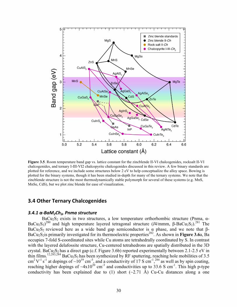
30
Figure 3.5. Room temperature band gap vs. lattice constant for the zincblende II-VI chalcogenides, rocksalt II-VI chalcogenides, and ternary I-III-VI2 chalcopyrite chalcogenides discussed in this review. A few binary standards are plotted for reference, and we include some structures below 2 eV to help conceptualize the alloy space. Bowing is plotted for the binary systems, though it has been studied in-depth for many of the ternary systems. We note that the zincblende structure is not the most thermodynamically stable polymorph for several of these systems (e.g. MnS, MnSe, CdS), but we plot zinc blende for ease of visualization. 3.4OtherTernaryChalcogenides 3.4.1α-BaM2Ch2,Pnmastructure
BaCu2S2 exists in two structures, a low temperature orthorhombic structure (Pnma, α-BaCu2S2)280 and high temperature layered tetragonal structure (I4/mmm, β-BaCu2S2).281 The BaCu2S2 reviewed here as a wide band gap semiconductor is α phase, and we note that β- BaCu2S2is primarily investigated for its thermoelectric properties282. As shown in Figure 3.6a, Ba occupies 7-fold S-coordinated sites while Cu atoms are tetrahedrally coordinated by S. In contrast with the layered delafossite structure, Cu-centered tetrahedrons are spatially distributed in the 3D crystal. BaCu2S2 has a direct gap (c.f. Figure 3.6b) reported experimentally between 2.1-2.5 eV in thin films.12,283,284 BaCu2S2 has been synthesized by RF sputtering, reaching hole mobilities of 3.5 cm2
V-1 s-1 at dopings of ~1019 cm-3, and a conductivity of 17 S cm-1,284 as well as by spin coating,
reaching higher dopings of ~4x1020 cm-3 and conductivities up to 33.6 S cm-1. This high p-type conductivity has been explained due to (1) short (~2.71 Å) Cu-Cu distances along a one

31
dimensional chain, allowing for a broad band along which hole conductivity takes place (c.f. Figure 3.6c),283 (2) hybridization of S 3p and Cu 4d states at the upper VB, resulting in low hole effective mass of ~0.8 me,285 (3) holes from VCu acceptors, and (4) its notably high ionization energy compared to other p-type chalcogenides (4.84 eV).286 The p-type conductivity is limited by VS donor defects.287 Combinatorial sputtering was used to explore the influence of off-stoichiometries and processing temperature on BaCu2S2 properties, as shown in Figure 3.6d,12 finding conductivity to increase from 0.1 to 53 S cm-1 as the film transforms from amorphous to crystalline at a processing temperature of 250 °C. Higher processing temperatures lead to a drop of conductivity and increase in absorption. Both Ba and Cu off-stoichiometry can increase the conductivity at high processing temperatures, though degenerate doping limits this effect at lower temperatures. The combination of reasonably high transparency, high p-type conductivity, and moderate processing temperatures makes α-BaCu2S2 a promising wide band gap chalcogenide semiconductor.
The semiconducting properties of BaCu2Se2 and BaCu2Te2 have also been characterized, but they are not discussed here due to their gaps below 2 eV.288 BaAg2S2 (I4/mmm, not to be confused with its P-3m1 polymorph) has been calculated with HSE to have a gap just greater than 2 eV, but its mobility and conductivity have not been explored experimentally.286 Other wide gap computational compounds in this structural family include SrCu2S2 (HSE gap 2.27 eV), and SrCu2Se2 (HSE gap 2.03 eV), which have formation energies just above the convex hull (0.054 eV/atom and 0.027 eV/atom, respectively) according to theoretical calculations,286 but are difficult to synthesize.12 It is possible that the Cu-Cu or Ag-Ag chains and hybridized VBMs would lead to high hole conductivities in these alternative structures as well.
Figure 3.6. (a) The α-BaCu2S2 unit cell, (b) electronic band structure of α- BaCu2S2 from the Materials Project database, with a scissor operation applied to align with experimental band gap, (c) 1D chains of Cu-S within the
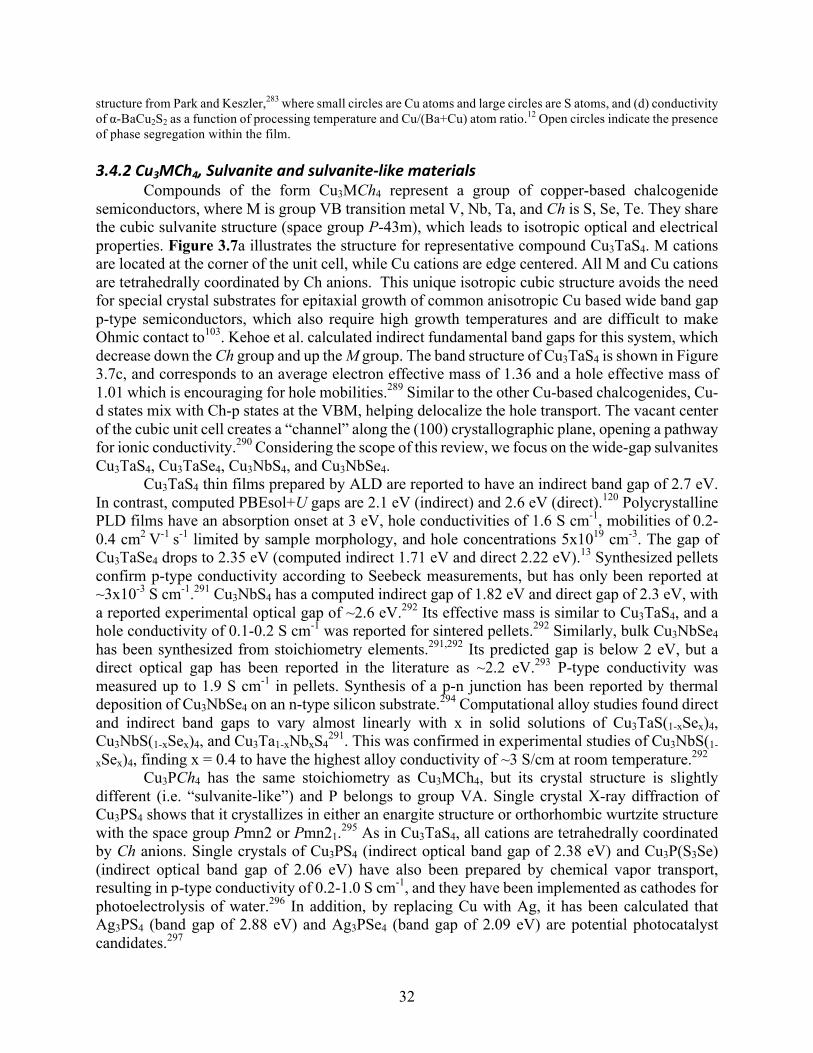
32
structure from Park and Keszler,283 where small circles are Cu atoms and large circles are S atoms, and (d) conductivity of α-BaCu2S2 as a function of processing temperature and Cu/(Ba+Cu) atom ratio.12 Open circles indicate the presence of phase segregation within the film.
3.4.2Cu3MCh4,Sulvaniteandsulvanite-likematerials
Compounds of the form Cu3MCh4 represent a group of copper-based chalcogenide semiconductors, where M is group VB transition metal V, Nb, Ta, and Ch is S, Se, Te. They share the cubic sulvanite structure (space group P-43m), which leads to isotropic optical and electrical properties. Figure 3.7a illustrates the structure for representative compound Cu3TaS4. M cations are located at the corner of the unit cell, while Cu cations are edge centered. All M and Cu cations are tetrahedrally coordinated by Ch anions. This unique isotropic cubic structure avoids the need for special crystal substrates for epitaxial growth of common anisotropic Cu based wide band gap p-type semiconductors, which also require high growth temperatures and are difficult to make Ohmic contact to103. Kehoe et al. calculated indirect fundamental band gaps for this system, which decrease down the Ch group and up the M group. The band structure of Cu3TaS4 is shown in Figure 3.7c, and corresponds to an average electron effective mass of 1.36 and a hole effective mass of 1.01 which is encouraging for hole mobilities.289 Similar to the other Cu-based chalcogenides, Cu-d states mix with Ch-p states at the VBM, helping delocalize the hole transport. The vacant center of the cubic unit cell creates a “channel” along the (100) crystallographic plane, opening a pathway for ionic conductivity.290 Considering the scope of this review, we focus on the wide-gap sulvanites Cu3TaS4, Cu3TaSe4, Cu3NbS4, and Cu3NbSe4.
Cu3TaS4 thin films prepared by ALD are reported to have an indirect band gap of 2.7 eV. In contrast, computed PBEsol+U gaps are 2.1 eV (indirect) and 2.6 eV (direct).120 Polycrystalline PLD films have an absorption onset at 3 eV, hole conductivities of 1.6 S cm-1, mobilities of 0.2-0.4 cm2
V-1 s-1 limited by sample morphology, and hole concentrations 5x1019 cm-3. The gap of
Cu3TaSe4 drops to 2.35 eV (computed indirect 1.71 eV and direct 2.22 eV).13 Synthesized pellets confirm p-type conductivity according to Seebeck measurements, but has only been reported at ~3x10⁻³ S cm-1.291 Cu3NbS4 has a computed indirect gap of 1.82 eV and direct gap of 2.3 eV, with a reported experimental optical gap of ~2.6 eV.292 Its effective mass is similar to Cu3TaS4, and a hole conductivity of 0.1-0.2 S cm-1 was reported for sintered pellets.292 Similarly, bulk Cu3NbSe4 has been synthesized from stoichiometry elements.291,292 Its predicted gap is below 2 eV, but a direct optical gap has been reported in the literature as ~2.2 eV.293 P-type conductivity was measured up to 1.9 S cm-1 in pellets. Synthesis of a p-n junction has been reported by thermal deposition of Cu3NbSe4 on an n-type silicon substrate.294 Computational alloy studies found direct and indirect band gaps to vary almost linearly with x in solid solutions of Cu3TaS(1-xSex)4, Cu3NbS(1-xSex)4, and Cu3Ta1-xNbxS4
291. This was confirmed in experimental studies of Cu3NbS(1-
xSex)4, finding x = 0.4 to have the highest alloy conductivity of ~3 S/cm at room temperature.292 Cu3PCh4 has the same stoichiometry as Cu3MCh4, but its crystal structure is slightly
different (i.e. “sulvanite-like”) and P belongs to group VA. Single crystal X-ray diffraction of Cu3PS4 shows that it crystallizes in either an enargite structure or orthorhombic wurtzite structure with the space group Pmn2 or Pmn21.295 As in Cu3TaS4, all cations are tetrahedrally coordinated by Ch anions. Single crystals of Cu3PS4 (indirect optical band gap of 2.38 eV) and Cu3P(S3Se) (indirect optical band gap of 2.06 eV) have also been prepared by chemical vapor transport, resulting in p-type conductivity of 0.2-1.0 S cm-1, and they have been implemented as cathodes for photoelectrolysis of water.296 In addition, by replacing Cu with Ag, it has been calculated that Ag3PS4 (band gap of 2.88 eV) and Ag3PSe4 (band gap of 2.09 eV) are potential photocatalyst candidates.297
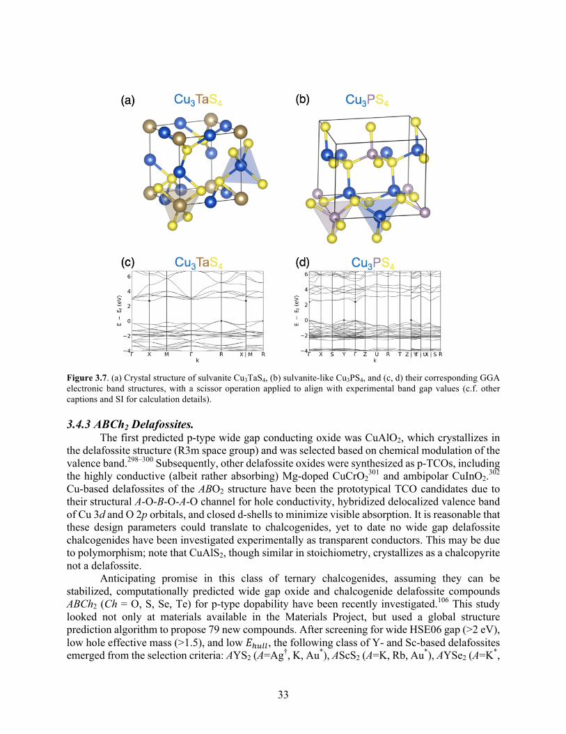
33
Figure 3.7. (a) Crystal structure of sulvanite Cu3TaS4, (b) sulvanite-like Cu3PS4, and (c, d) their corresponding GGA electronic band structures, with a scissor operation applied to align with experimental band gap values (c.f. other captions and SI for calculation details). 3.4.3 ABCh2 Delafossites.
The first predicted p-type wide gap conducting oxide was CuAlO2, which crystallizes in the delafossite structure (R3m space group) and was selected based on chemical modulation of the valence band.298–300 Subsequently, other delafossite oxides were synthesized as p-TCOs, including the highly conductive (albeit rather absorbing) Mg-doped CuCrO2
301 and ambipolar CuInO2.302 Cu-based delafossites of the ABO2 structure have been the prototypical TCO candidates due to their structural A-O-B-O-A-O channel for hole conductivity, hybridized delocalized valence band of Cu 3d and O 2p orbitals, and closed d-shells to minimize visible absorption. It is reasonable that these design parameters could translate to chalcogenides, yet to date no wide gap delafossite chalcogenides have been investigated experimentally as transparent conductors. This may be due to polymorphism; note that CuAlS2, though similar in stoichiometry, crystallizes as a chalcopyrite not a delafossite.
Anticipating promise in this class of ternary chalcogenides, assuming they can be stabilized, computationally predicted wide gap oxide and chalcogenide delafossite compounds ABCh2 (Ch = O, S, Se, Te) for p-type dopability have been recently investigated.106 This study looked not only at materials available in the Materials Project, but used a global structure prediction algorithm to propose 79 new compounds. After screening for wide HSE06 gap (>2 eV), low hole effective mass (>1.5), and low 𝐸'()), the following class of Y- and Sc-based delafossites emerged from the selection criteria: AYS2 (A=Ag†, K, Au*), AScS2 (A=K, Rb, Au*), AYSe2 (A=K*,
34
Cs), KScSe2*, and BaCaTe2
*, with a * indicating a new material not present in the ICSD or Materials Project database and † indicating a structure which, during the computation, transformed from delafossite to another, more stable structure (c.f. SI). In particular, AgYS2 was recommended for synthesis, with an HSE gap of 3.16 eV and a hole effective mass of 0.71. The crystal structure of another promising compound, KYS2, is shown in Figure 3.8 for reference. Branch point energy calculations revealed mid-gap Fermi stabilization energies for nearly all of these compounds, which is, as discussed in Section 2.4.1, not conclusive of doping type and thus defect calculations are still needed. This study is aimed towards finding p-type transparent conductors, but predicted structures could also be used for other applications (e.g. for their predicted magnetic properties).
3.4.4 ABCh3, Perovskites.
Perovskites are another class of ternary materials common as both n-type and p-type transparent conducting oxides, e.g. n-type CdSnO3 (CTO), 303 n-type La:BaSnO3,304 p-type In:SrTiO3 (ISTO),305 and p-type LaCrO3.306 A computational study screening for new sulfide perovskite materials as photoelectrochemical (PEC) absorbers discovered several compounds with wide gaps (EG > 2 eV) and low hole effective masses (m* < 1) that could be investigated as p-type transparent conductors, including BaZrS3 (c.f. Figure 3.8), BiGaS3, BiScS3, CaZrS3 and ZrCdS3 (c.f. SI for other compounds and more information).307 These structures were screened for defect tolerance to ensure no defect states were present in the middle of the gap, though p-type dopability was not confirmed and remains to be investigated. This theoretical study motivates further experimental investigation of such materials and exploration of perovskite selenides and tellurides.
3.4.5 A2B3Ch4 and Dimensional reduction.
With the exception of the materials discussed in Section 3.1, many binary chalcogenides exhibit gaps lower than 2 eV. Dimensional reduction is an interesting strategy to expand the space of wide band gap ternary compounds, by starting with low band gap binary constituents and widening their gaps.308 For example, low gap binary chalcogenides MCh (Ch = S, Se, Te) can achieve a wider gap by admixing with Cs2Ch to effectively reduce dimensionality (i.e. introduce layers) and reduce orbital overlap. A tradeoff of this procedure, however, is a decreased dispersion due to weakened covalent bonding and thus larger hole effective masses, which is the opposite trend than going from II-Ch to I-III-Ch2 material systems. Based on this method, a dimensional reduction on ZnCh and Cs2Ch was performed, and Cs2Zn3Se4 (c.f. Figure 3.8) and Cs2Zn3Te4 ternaries were proposed as promising p-type TCs, with HSE06 gaps of 3.61 eV and 2.82 eV and hole effective masses of 1.23 and 1.25, respectively. Undoped Cs2Zn3Se4 and Cs2Zn3Te4 were found to be intrinsically p-type materials. However, the free hole concentration may be limited by low energy of native donor defects, e.g., Zn interstitials.309 Another dimensional reduction study with HgCh proposed Tl2Hg3S4 and K2Hg3S4 with gaps 2.22 eV and 2.2-2.6 eV, respectively.310 The dimensional reduction strategy has only been applied to a few classes of binary chalcogenides, which have yet to be explored experimentally, so this strategy could benefit from further exploration.
KYS2 BaZrS3 Cs2Zn3Se4* La2O2Se ZrOS
R-32/m
delafossite
Pnma
perovskite Ibam
P-3m1
oxyselenide
P213
oxysulfide
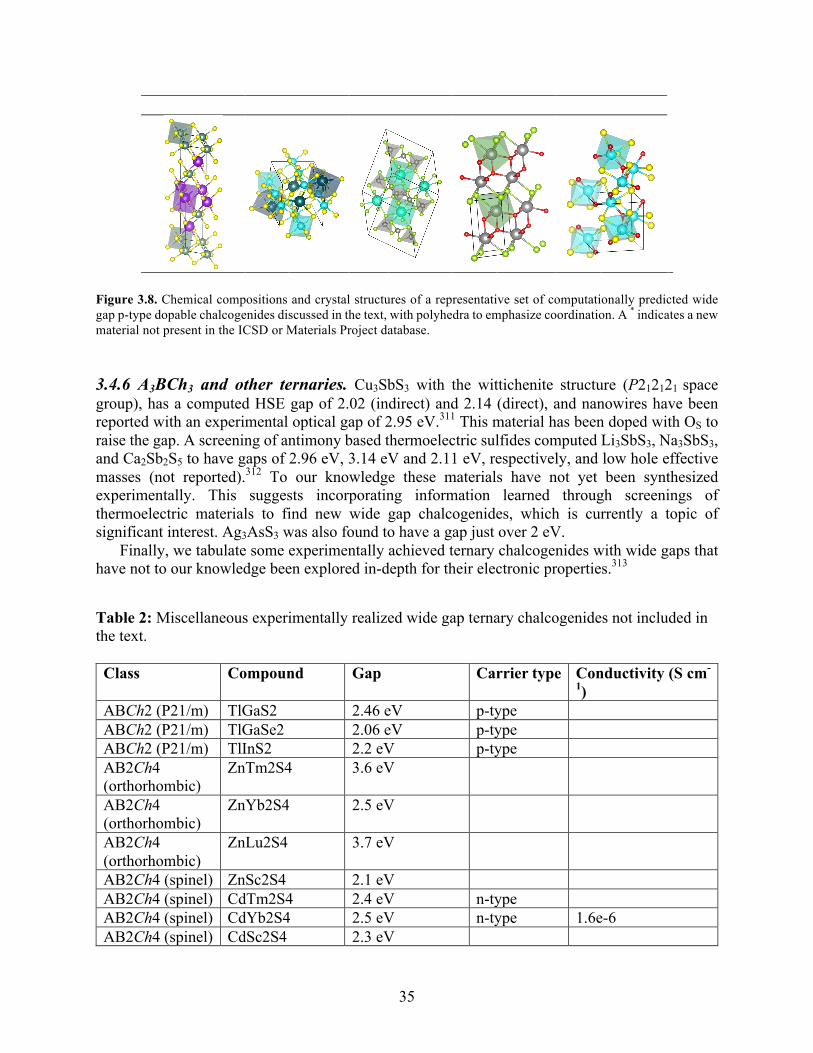
35
Figure 3.8. Chemical compositions and crystal structures of a representative set of computationally predicted wide gap p-type dopable chalcogenides discussed in the text, with polyhedra to emphasize coordination. A * indicates a new material not present in the ICSD or Materials Project database. 3.4.6 A3BCh3 and other ternaries. Cu3SbS3 with the wittichenite structure (P212121 space group), has a computed HSE gap of 2.02 (indirect) and 2.14 (direct), and nanowires have been reported with an experimental optical gap of 2.95 eV.311 This material has been doped with OS to raise the gap. A screening of antimony based thermoelectric sulfides computed Li3SbS3, Na3SbS3, and Ca2Sb2S5 to have gaps of 2.96 eV, 3.14 eV and 2.11 eV, respectively, and low hole effective masses (not reported).312 To our knowledge these materials have not yet been synthesized experimentally. This suggests incorporating information learned through screenings of thermoelectric materials to find new wide gap chalcogenides, which is currently a topic of significant interest. Ag3AsS3 was also found to have a gap just over 2 eV.
Finally, we tabulate some experimentally achieved ternary chalcogenides with wide gaps that have not to our knowledge been explored in-depth for their electronic properties.313 Table 2: Miscellaneous experimentally realized wide gap ternary chalcogenides not included in the text. Class Compound Gap Carrier type Conductivity (S cm-
1) ABCh2 (P21/m) TlGaS2 2.46 eV p-type ABCh2 (P21/m) TlGaSe2 2.06 eV p-type ABCh2 (P21/m) TlInS2 2.2 eV p-type AB2Ch4 (orthorhombic)
ZnTm2S4 3.6 eV
AB2Ch4 (orthorhombic)
ZnYb2S4 2.5 eV
AB2Ch4 (orthorhombic)
ZnLu2S4 3.7 eV
AB2Ch4 (spinel) ZnSc2S4 2.1 eV AB2Ch4 (spinel) CdTm2S4 2.4 eV n-type AB2Ch4 (spinel) CdYb2S4 2.5 eV n-type 1.6e-6 AB2Ch4 (spinel) CdSc2S4 2.3 eV
36
ABCh3 LaGaSe3 2.1 eV ~10-6 ABCh3 CeGaSe3 2.2 eV ~10-6 ABCh3 PrGaSe3 2.14 eV ~10-6 ABCh3 NdGaSe3 2.16 eV ~10-6 ABCh3 SmGaSe3 2.0 eV ~10-6
3.5Quaternaryandmixedanionchalcogenides Mixing chalcogenides with oxygen or anions from other groups like fluorine, typically in layered motifs, results in wide band gap mixed anion chalcogenides e.g. LnCuOCh (Ln=La, Pr, Nd), MCuChF (M=Ba, Sr). 3.5.1 LnCuOCh. We limit our discussion to LaCuOCh as a representative of oxychalcogenides LnCuOCh in this review, since it has been most heavily investigated. (Pr,Nd)CuOCh have similar optoelectrical properties including band gap and p-type doping, but chalcogen type significantly influences carrier concentration as shown in Figure 3.9d.314 Reported conductivities are in the planar direction. We note that these compounds are difficult to make Ohmic contact with, due to their layered, anisotropic structure. LaCuOS thin films have been prepared by RF-sputtering with a direct band gap of 3.1 eV, and p-type conductivity confirmed by positive Seebeck coefficients.315 Its undoped conductivity of 1.2x10⁻² S cm-1 can be increased to 2.6x10⁻¹ S cm-1 by partial substitution of La with divalent cations like Sr2+ 316. Figure 3.9a shows the alternative stacking of La-O and Cu-S layers
By substituting the S with Se, LaCuOS1-xSex (x=0.0, 0.25, 0.5, 0.75, and 1.0) solid solutions have been demonstrated, including LaCuOSe. It was found that the band gap decreases from ~3.1 to ~2.8 eV as x increases from 0 to 1, but remains direct,317 and Figure 3.9b illustrates the increased valence band dispersion in LaCuOSe. Epitaxial LaCuOS1-xSex thin films were prepared to investigate hole transport properties. The Hall mobility increased with x between ~0.5 cm2
V-1 s-1
for LaCuOS and 8 cm2 V-1
s-1 for LaCuOSe. This mobility is high for typical p-type transparent conductors, and the increase with x is expected since the valence band should be more disperse with Se 4p orbital. The hole concentrations in undoped LaCuOS1-xSex are around 1019 cm-3 to 1020 cm-3, so the doping is close to degenerate. Mg can degenerately dope LaCuOSe, increasing the carrier concentration by an order (up to 2x1020 cm-3) while only decreasing the mobility by half, and raising the conductivity up to a reported 140 S cm-1.318 The layered structure induces a distinctive conduction mechanism in LaCuOSe. It was initially proposed that hole generation occurs in the (La2O2)2+ layer, then holes are transported through the (Cu2Ch2)2- layer (hole conduction layer), successfully avoiding the influence of ionized impurity scattering.319 It was later suggested that the heavy hole doping from Mg may be due to the off-stoichiometry of Cu and Se rather than Mg doping at the La sites, and Mg ions may enhance the generation of Cu and Se deficiencies. No reports of n-type conductivity could be found.
Unlike LaCuOS and LaCuOSe, LaCuOTe has an indirect band gap due to the stronger La-Te interactions compared with other the La-Ch.320 Comparison of the experimental and theoretical XRD patterns for LaCuOTe is shown in Fig.3.9b, to demonstrate that the sample is single phase without other impurities.321 Synthesis of a ceramic pellet of LaCuOTe revealed an optical band
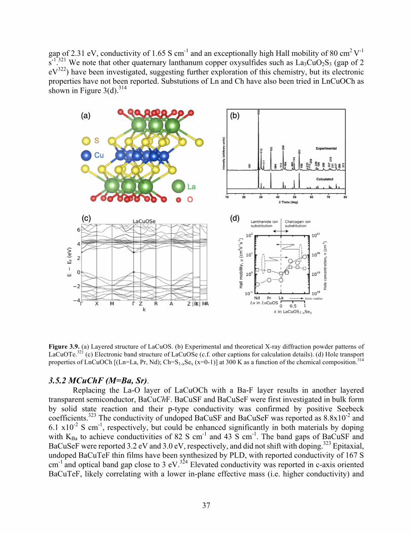
37
gap of 2.31 eV, conductivity of 1.65 S cm-1 and an exceptionally high Hall mobility of 80 cm2 V-1
s-1.321 We note that other quaternary lanthanum copper oxysulfides such as La3CuO2S3 (gap of 2 eV322) have been investigated, suggesting further exploration of this chemistry, but its electronic properties have not been reported. Substutions of Ln and Ch have also been tried in LnCuOCh as shown in Figure 3(d).314
Figure 3.9. (a) Layered structure of LaCuOS. (b) Experimental and theoretical X-ray diffraction powder patterns of LaCuOTe.321 (c) Electronic band structure of LaCuOSe (c.f. other captions for calculation details). (d) Hole transport properties of LnCuOCh [(Ln=La, Pr, Nd); Ch=S1-xSex (x=0-1)] at 300 K as a function of the chemical composition.314
3.5.2 MCuChF (M=Ba, Sr).
Replacing the La-O layer of LaCuOCh with a Ba-F layer results in another layered transparent semiconductor, BaCuChF. BaCuSF and BaCuSeF were first investigated in bulk form by solid state reaction and their p-type conductivity was confirmed by positive Seebeck coefficients.323 The conductivity of undoped BaCuSF and BaCuSeF was reported as 8.8x10⁻² and 6.1 x10⁻² S cm-1, respectively, but could be enhanced significantly in both materials by doping with KBa to achieve conductivities of 82 S cm-1 and 43 S cm-1. The band gaps of BaCuSF and BaCuSeF were reported 3.2 eV and 3.0 eV, respectively, and did not shift with doping.323 Epitaxial, undoped BaCuTeF thin films have been synthesized by PLD, with reported conductivity of 167 S cm-1 and optical band gap close to 3 eV.324 Elevated conductivity was reported in c-axis oriented BaCuTeF, likely correlating with a lower in-plane effective mass (i.e. higher conductivity) and
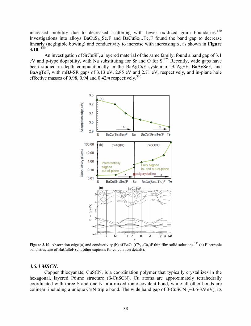
38
increased mobility due to decreased scattering with fewer oxidized grain boundaries.120 Investigations into alloys BaCuS1-xSexF and BaCuSe1-xTexF found the band gap to decrease linearly (negligible bowing) and conductivity to increase with increasing x, as shown in Figure 3.10. 150
An investigation of SrCuSF, a layered material of the same family, found a band gap of 3.1 eV and p-type dopability, with Na substituting for Sr and O for S.325 Recently, wide gaps have been studied in-depth computationally in the BaAgChF system of BaAgSF, BaAgSeF, and BaAgTeF, with mBJ-SR gaps of 3.13 eV, 2.85 eV and 2.71 eV, respectively, and in-plane hole effective masses of 0.98, 0.94 and 0.42m respectively.326
Figure 3.10. Absorption edge (a) and conductivity (b) of BaCu(Ch1-xChx)F thin film solid solutions.150 (c) Electronic band structure of BaCuSeF (c.f. other captions for calculation details). 3.5.3 MSCN.
Copper thiocyanate, CuSCN, is a coordination polymer that typically crystallizes in the hexagonal, layered P63mc structure (β-CuSCN). Cu atoms are approximately tetrahedrally coordinated with three S and one N in a mixed ionic-covalent bond, while all other bonds are colinear, including a unique C≡N triple bond. The wide band gap of β-CuSCN (~3.6-3.9 eV), its
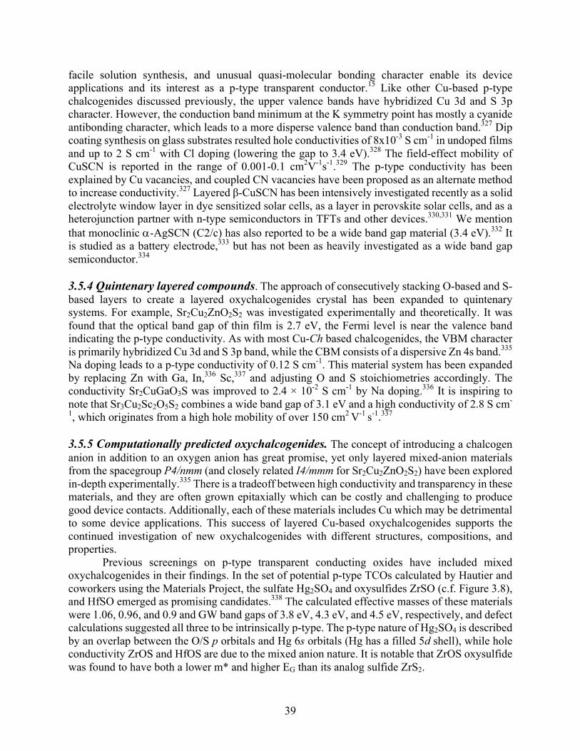
39
facile solution synthesis, and unusual quasi-molecular bonding character enable its device applications and its interest as a p-type transparent conductor.15 Like other Cu-based p-type chalcogenides discussed previously, the upper valence bands have hybridized Cu 3d and S 3p character. However, the conduction band minimum at the K symmetry point has mostly a cyanide antibonding character, which leads to a more disperse valence band than conduction band.327 Dip coating synthesis on glass substrates resulted hole conductivities of 8x10⁻³ S cm-1 in undoped films and up to 2 S cm-1 with Cl doping (lowering the gap to 3.4 eV).328 The field-effect mobility of CuSCN is reported in the range of 0.001-0.1 cm2V-1s-1.329 The p-type conductivity has been explained by Cu vacancies, and coupled CN vacancies have been proposed as an alternate method to increase conductivity.327 Layered β-CuSCN has been intensively investigated recently as a solid electrolyte window layer in dye sensitized solar cells, as a layer in perovskite solar cells, and as a heterojunction partner with n-type semiconductors in TFTs and other devices.330,331 We mention that monoclinic a-AgSCN (C2/c) has also reported to be a wide band gap material (3.4 eV).332 It is studied as a battery electrode,333 but has not been as heavily investigated as a wide band gap semiconductor.334 3.5.4 Quintenary layered compounds. The approach of consecutively stacking O-based and S-based layers to create a layered oxychalcogenides crystal has been expanded to quintenary systems. For example, Sr2Cu2ZnO2S2 was investigated experimentally and theoretically. It was found that the optical band gap of thin film is 2.7 eV, the Fermi level is near the valence band indicating the p-type conductivity. As with most Cu-Ch based chalcogenides, the VBM character is primarily hybridized Cu 3d and S 3p band, while the CBM consists of a dispersive Zn 4s band.335 Na doping leads to a p-type conductivity of 0.12 S cm-1. This material system has been expanded by replacing Zn with Ga, In,336 Sc,337 and adjusting O and S stoichiometries accordingly. The conductivity Sr2CuGaO3S was improved to 2.4 × 10⁻² S cm-1 by Na doping.336 It is inspiring to note that Sr3Cu2Sc2O5S2 combines a wide band gap of 3.1 eV and a high conductivity of 2.8 S cm-
1, which originates from a high hole mobility of over 150 cm2 V-1
s-1.337 3.5.5 Computationally predicted oxychalcogenides. The concept of introducing a chalcogen anion in addition to an oxygen anion has great promise, yet only layered mixed-anion materials from the spacegroup P4/nmm (and closely related I4/mmm for Sr2Cu2ZnO2S2) have been explored in-depth experimentally.335 There is a tradeoff between high conductivity and transparency in these materials, and they are often grown epitaxially which can be costly and challenging to produce good device contacts. Additionally, each of these materials includes Cu which may be detrimental to some device applications. This success of layered Cu-based oxychalcogenides supports the continued investigation of new oxychalcogenides with different structures, compositions, and properties.
Previous screenings on p-type transparent conducting oxides have included mixed oxychalcogenides in their findings. In the set of potential p-type TCOs calculated by Hautier and coworkers using the Materials Project, the sulfate Hg2SO4 and oxysulfides ZrSO (c.f. Figure 3.8), and HfSO emerged as promising candidates.338 The calculated effective masses of these materials were 1.06, 0.96, and 0.9 and GW band gaps of 3.8 eV, 4.3 eV, and 4.5 eV, respectively, and defect calculations suggested all three to be intrinsically p-type. The p-type nature of Hg2SO4 is described by an overlap between the O/S p orbitals and Hg 6s orbitals (Hg has a filled 5d shell), while hole conductivity ZrOS and HfOS are due to the mixed anion nature. It is notable that ZrOS oxysulfide was found to have both a lower m* and higher EG than its analog sulfide ZrS2.
40
Sarmadian et al. screened all oxides in the AFLOWLIB library (12,211 total compounds) for low effective mass and wide band gap, and also included branch point energy (BPE) calculations as a proxy for p-type dopability.88 Interestingly, out of all the oxides screened, oxychalcogenide materials proved to be the most promising. In particular, this study identified the class of P3m1 lanthanide oxyselenides, X2SeO2 (X = La, Pr, Nd, Gd) to be the most viable candidates. Their disperse valence band (m* between 0.69 and 0.92), wide gap (HSE06 gaps of 2.76 - 3.49 eV), and charge neutrality levels at or near the valence band are all promising for wide band gap p-type semiconductor applications. La2O2Se (c.f. Figure 3.8) was studied in greater depth using defect formation energy calculations, suggesting that in anion-rich conditions Na substitution for La should produce a p-type conductivity without compensation from anion vacancies. If realized experimentally, this material could pose as an isotropic, Cu-free alternative to LaCuOSe. Additionally, this study revealed the following materials to consider for future investigation: Tb2Ti2S2O5, NaVS2O8, Hg2SO4, Hg2SeO3, Ba3Bi2TeO9, and CaTe3O8 (though Hg-containing compounds are impractical; see SI for computed properties). Additionally, oxychalcogenides Gd2O2Se and Y2OS2 and mixed anion Pb(NCS)2, among others, have been identified as potential scintillator materials, each with a low hole effective mass and a relatively wide band gap.105 Overall, oxychalcogenides clearly pose a promising direction for future research. However, they also pose unique challenges in terms of synthesis and stability that must be addressed to advance the field. 3.5.6Quaternarysingle-anioncompounds.
There have been reports of quaternary Ln-based chalcogenides focusing on basic synthesis and crystal structure, but not many published investigations of optoelectronic properties. These materials usually consist of alkali or alkali-metal, rare-earth metal (Ln), transitional metal like Cu/Ag/Zn and chalcogen in the formation of (K, Rb, Cs, Ba, Sr, Cd, Mg)/Ln/(Cu, Ag, Zn)/Ch.339–
341 Here we point out the basic principle of the property changes depending on the composition, mainly from wide band gap compounds. (1) Compounds consisting of different Lanthanum series are not necessary to perform the same band gaps in similar crystal structures, like the optical band gap changes by more than 0.75 eV with different Lanthanum elements in CsLnZnSe3.342 (2) Crystal orientation has a slight effect on optical band gap. CsSmZnSe3 has a wide band gap of 2.63 eV for the (010) crystal face and 2.56 eV for the (001) crystal face.342 3.62Dchalcogenides 2D chalcogenide semiconductors have been heavily investigated in recent years due to their unique properties resulting from 2D confinement. We will briefly discuss the optical and electronic properties of wide gap 2D chalcogenides here, though they have been extensively reviewed elsewhere.343,344,345 2D materials typically possess weak interlayer van der Waals (vdW) forces with strong in-plane covalent bonds but are not limited to this configuration. For example, several oxide-based bulk materials can be exfoliated into atomically thin crystals, e.g. MoO3 and WO3, while in other cases the stoichiometry can differ from bulk form, e.g., TiO2.346 2D chalcogenides appear to be more favorable than 2D oxides for electronic applications due to their tunable band gaps and mobilities. Monolayer oxides tend to have larger band gaps and lower dielectric constants compared to their bulk forms,346,347 which indicates that thinning a 2D chalcogenide could be advantageous to attaining larger band gaps or higher transparency under visible light. In this
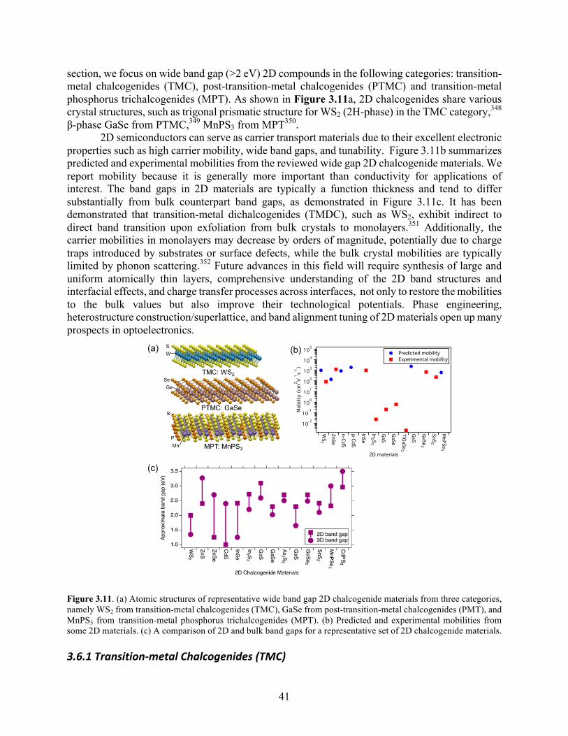
41
section, we focus on wide band gap (>2 eV) 2D compounds in the following categories: transition-metal chalcogenides (TMC), post-transition-metal chalcogenides (PTMC) and transition-metal phosphorus trichalcogenides (MPT). As shown in Figure 3.11a, 2D chalcogenides share various crystal structures, such as trigonal prismatic structure for WS2 (2H-phase) in the TMC category,348 β-phase GaSe from PTMC,349 MnPS3 from MPT350. 2D semiconductors can serve as carrier transport materials due to their excellent electronic properties such as high carrier mobility, wide band gaps, and tunability. Figure 3.11b summarizes predicted and experimental mobilities from the reviewed wide gap 2D chalcogenide materials. We report mobility because it is generally more important than conductivity for applications of interest. The band gaps in 2D materials are typically a function thickness and tend to differ substantially from bulk counterpart band gaps, as demonstrated in Figure 3.11c. It has been demonstrated that transition-metal dichalcogenides (TMDC), such as WS2, exhibit indirect to direct band transition upon exfoliation from bulk crystals to monolayers.351 Additionally, the carrier mobilities in monolayers may decrease by orders of magnitude, potentially due to charge traps introduced by substrates or surface defects, while the bulk crystal mobilities are typically limited by phonon scattering.352 Future advances in this field will require synthesis of large and uniform atomically thin layers, comprehensive understanding of the 2D band structures and interfacial effects, and charge transfer processes across interfaces, not only to restore the mobilities to the bulk values but also improve their technological potentials. Phase engineering, heterostructure construction/superlattice, and band alignment tuning of 2D materials open up many prospects in optoelectronics.
Figure 3.11. (a) Atomic structures of representative wide band gap 2D chalcogenide materials from three categories, namely WS2 from transition-metal chalcogenides (TMC), GaSe from post-transition-metal chalcogenides (PMT), and MnPS3 from transition-metal phosphorus trichalcogenides (MPT). (b) Predicted and experimental mobilities from some 2D materials. (c) A comparison of 2D and bulk band gaps for a representative set of 2D chalcogenide materials. 3.6.1Transition-metalChalcogenides(TMC)
(a) (b)
(c)
10-2
10-1
100
101
102
103
104
105
Mob
ility
(cm
2 V-1s-1
)
WS
2
ZnSe
n-CdS
p-CdS
InSe
In2 S
3
GaS
GaSe
TlGaSe2
GeS
GeSe2
SnS2
MnPSe
3
2D materials
Predicted mobility Experimental mobility
42
WS2 in the 2H-polytype structure is an n-type indirect gap semiconductor with a band gap of ~1.35 eV.353 Strong photoluminescence has been demonstrated from monolayer WS2 due to the transition from its bulk indirect band gap to its monolayer direct band gap,366,355 which is ~2 eV at room temperature.356 Monolayer WS2 provides the widest band gap and highest predicted phonon-limited mobility (over 1000 cm2
V-1 s-1) among TMDCs (MX2, M= W, Mo, X= S, Se, Te) at room
temperature.357 Due to defects, charge traps, and Coulomb impurities, reported experimental mobility of monolayer WS2 is only 83 cm2
V-1 s-1, even after improvements via a combination of a
thin layer of Al2O3 and thiol chemical functionalization.358 It has been shown that in gated charge transport measurements, mechanically exfoliated monolayer WS2 with a nitrogen plasma treatment have higher electron mobility (184.2 cm2
V-1 s-1) than the scalable metal-organic CVD
monolayer WS2 (30 cm2 V-1
s-1) at room temperature,359,360 which reflects that there is still room to improve the synthesis of monolayer WS2.361 One recent strategy to improve monolayer mobility is doping with other transition metals, such as V and Zr.362 The thin layer nature of monolayer WS2 opens up the possibility of manipulating its band structure by forming heterostructures. It is observed that conductivity enhancement and band bending occurs at the interface of WS2 based heterojunctions.363 2D WS2 has been explored as a hole-transport layer in perovskite solar cells, demonstrating higher performance and better stability than transitional conductive polymers.364,365 ZnS has a gap of ~3.7-3.8 eV (zinc blende) in bulk form, as discussed in Section 3.1.1. Here, we highlight its possible function as a wide band gap semiconductor in atomic thin form. DFT calculations predict the 2D a wide band gap of 2.07 with Generalized Gradient Approach (GGA) functional, or 2.77 eV with Perdew, Burkeand Ernzerhof (PBE)-GGA functional.366 Hydrothermal synthesized ZnS nanoparticles with 15-25 nm suggest a wider gap in the range of ~3.9-4.8 eV.367 Monolayer ZnSe, a direct band gap semiconductor with a pseudo-hexagonal (ph) lattice structure,368,369 demonstrates a high carrier mobility of 1250 cm2
V-1 s-1 and generates a much higher photocurrent than in its bulk form.370 The DFT calculated band gap of ph-ZnSe is reported to be 1.25 eV based on the atomic structural parameters by X-ray absorption fine structure (XAFS).370 A tetragonal structure ZnSe (t-ZnSe) has been predicted under lateral pressure, with a wide band gap of 2-3 eV and retention of its direct character up to 7% biaxial strain.371 A computed electron mobility of t-ZnSe is ~138.8 cm2
V-1 s-1, making it a possible n-type channel material.371 CdS is also discussed previously as a wide band gap bulk semiconductor (~2.4 eV).372
Several studies have investigated the synthesis and characterization of colloidal 2D nanosheets of CdS and CdS1-xSex.373,374 CdS nanosheets and nanoparticles have been intensively studied for photocatalysis by assembling into heterojunctions with other 2D materials, e.g., graphene/graphene oxide,375,376,377 MoS2,378,379 ZnSe,380 etc., and monolayers or nanosheets can be stacked sequentially to form heterostructures. CdS/ZnSe in-plane heterostructures are predicted by HSE06 to have type-II band alignment and 2.31 eV direct band gap with the “armchair configuration”, which has electron and hole mobilities of ~884 cm2
V-1 s-1 and ~1920 cm2 V-1 s-1,
respectively.380 3.6.2PostTransition-metalChalcogenides(PTMC) The band gap of monolayer InSe is calculated to be 2.41 eV by DFT with the screened exchange (sX) hybrid density functional, in contrast to its calculated bulk indirect gap of 1.2-1.3 eV.381 Predicted electron mobilities in atomically thin InSe are above 103 cm2
V-1 s-1.382,383 2D InSe inherits the advantage properties of bulk InSe, such as a low electron effective-mass and shallow dopant sites.381,383 Several studies using InSe in optoelectronic applications have shown promising characteristics.384,385 GaS in bulk form has a PBE version of GGA predicted indirect band gap of
43
1.59 eV and a direct band gap of 2.59 eV.386 Another first-principles study predicts a direct band gap of 1.785 eV in monolayer GaS but a direct gap of 2.035 eV in bilayer GaS (less than 0.2 eV above its indirect band gap).387 Bulk GaS has hole mobility of about 80 cm2
V-1s-1,388 while the reported electron mobility for 1.5 nm thick GaS is 0.2 cm2
V-1s-1.389 As a transistor, thin GaS demonstrates typical n-type conductance behavior with an on/off ratio of 104.390 The band gap calculation and mobility experimental results enable GaS nanosheets as possible photodetectors.387
Monolayer GeS has a DFT via the plane-wave technique embedded Vienna ab initio simulation package (VASP) predicted electron mobility of 2950 to 3680 cm2
V-1 s-1, depending on
the axis direction, and an indirect band gap of 2.34 eV391, in contrast to a GGA of PBE calculated electron mobility of 2430 cm2
V-1 s-1 and an HSE06 predicted indirect band gap as 2.29 eV. 391,392.
Both external electric field and strain can tune the band gap.393 Several studies have theoretical calculated monolayer GeS for potential applications, such as gas sensor,394 catalysis,395 and photocatalysis.396
3D single crystal SnS2 is a p-type semiconductor with a band gap of ~2.1 eV, as discussed previously.397,398 HSE06 hybrid functional predicts monolayer SnS2 to have an indirect band gap of 2.41 eV.399 A monolayer SnS2 FET demonstrates n-type conduction,400 with an electron mobility of ~5 cm2
V-1 s-1 reported at room temperature for exfoliated few-layer SnS2. The FET devices in solution provides enhanced carrier mobilities up to 230 cm2
V-1 s-1.401 This result emphases the sensitivity of the electronic properties of an atomic thin material on surface interactions. The n-type semiconductor β- In2S3 has a reported band gap of 2.3 eV in thin film form and is the stable phase at room temperature.402 Synthesis of thin β-In2S3 nanosheets based on aqueous solution routes and CVD methods have been reported.403–405 A photodetector based on β-In2S3 nanosheets has demonstrated a high responsivity and external quantum efficiency, while the calculated carrier mobility is 0.023 cm2
V-1 s-1 with an on/off ratio of 1.5×103.405 Bulk As2S3 is
known as the mineral orpiment and a yellow pigment with a non-perfect flat layered structure, and is p-type semiconductor with a band gap of 2.5 eV.406 DFT predicts an indirect band gap of 2.12-3.18 eV for monolayer As2S3, and is affected by layer thickness and external strains as observed in other 2D chalcogenides. 406
Bulk TlInS2, TlGaSe2, TlGaS2 from the ternary thallium chalcogenide family TlMX2 (M= Ga or In, X= S or Se) have wide band gaps of >2 eV.407,408,409 These compounds share a quasi-two-dimensional layered structure in bulk form, and potentially can be exfoliated to atomic-thick layers.408 The field-effect mobility of a thin TlGaSe2 sheet (~220 nm) was reported at 2.1 ×10⁻³
cm2
V-1 s-1 with a DFT calculated band gap of 1.95 eV.410 Recently, a high-through screening suggest MgAl2S4, as a layer-structured ternary chalcogenide material possessing direct bandgaps of 2.015 eV, as calculated by PBE functional, is stable in its monolayer form. 411 3.6.3MetalPhosphorusTrichalcogenides(MPT) MPS3 (M= Fe, Mn, Ni, Cd, and Zn) and MPSe3 (M=Fe and Mn) constitute another family of layered 2D chalcogenides, some of whcih have been synthesized or exfoliated into monolayers.350 The optical band gaps of monolayer MPS3 and MPSe3 materials vary from 1.3 to 3.5 eV, potentially suitable for photoelectric applications.350 For example, monolayer MnPSe3 is predicted as a potential material for spintronic devices with electrically controllable spin polarization, while monolayer Ag0.5Sc0.5PSe3 can serve as an efficient photocatalyst for water splitting.412,413 The HSE calculated single layer band gaps of CdPS3 and CdPSe3 are 3.30 eV and 2.25 eV, respectively. PBE functional monolayer gaps are 1.93 eV and 1.29 eV, respectively, while
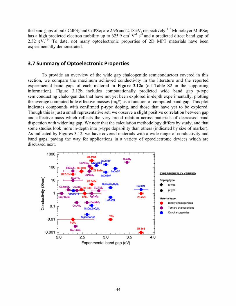
44
the band gaps of bulk CdPS3 and CdPSe3 are 2.96 and 2.18 eV, respectively.412 Monolayer MnPSe3 has a high predicted electron mobility up to 625.9 cm2
V-1 s-1 and a predicted direct band gap of 2.32 eV.414 To date, not many optoelectronic properties of 2D MPT materials have been experimentally demonstrated. 3.7SummaryofOptoelectronicProperties To provide an overview of the wide gap chalcogenide semiconductors covered in this section, we compare the maximum achieved conductivity in the literature and the reported experimental band gaps of each material in Figure 3.12a (c.f Table S2 in the supporting information). Figure 3.12b includes computationally predicted wide band gap p-type semiconducting chalcogenides that have not yet been explored in-depth experimentally, plotting the average computed hole effective masses (mh*) as a function of computed band gap. This plot indicates compounds with confirmed p-type doping, and those that have yet to be explored. Though this is just a small representative set, we observe a slight positive correlation between gap and effective mass which reflects the very broad relation across materials of decreased band dispersion with widening gap. We note that the calculation methodology differs by study, and that some studies look more in-depth into p-type dopability than others (indicated by size of marker). As indicated by Figures 3.12, we have covered materials with a wide range of conductivity and band gaps, paving the way for applications in a variety of optoelectronic devices which are discussed next.
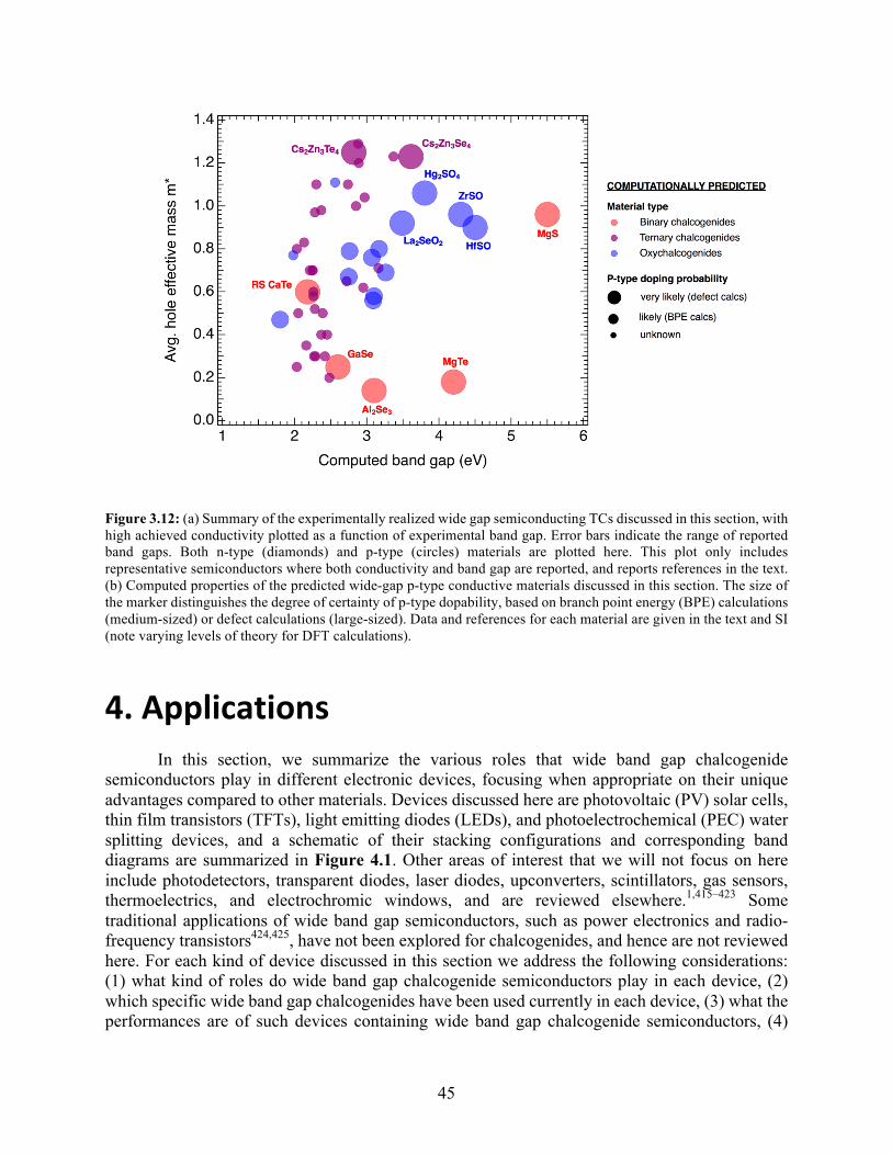
45
Figure 3.12: (a) Summary of the experimentally realized wide gap semiconducting TCs discussed in this section, with high achieved conductivity plotted as a function of experimental band gap. Error bars indicate the range of reported band gaps. Both n-type (diamonds) and p-type (circles) materials are plotted here. This plot only includes representative semiconductors where both conductivity and band gap are reported, and reports references in the text. (b) Computed properties of the predicted wide-gap p-type conductive materials discussed in this section. The size of the marker distinguishes the degree of certainty of p-type dopability, based on branch point energy (BPE) calculations (medium-sized) or defect calculations (large-sized). Data and references for each material are given in the text and SI (note varying levels of theory for DFT calculations).
4.Applications In this section, we summarize the various roles that wide band gap chalcogenide semiconductors play in different electronic devices, focusing when appropriate on their unique advantages compared to other materials. Devices discussed here are photovoltaic (PV) solar cells, thin film transistors (TFTs), light emitting diodes (LEDs), and photoelectrochemical (PEC) water splitting devices, and a schematic of their stacking configurations and corresponding band diagrams are summarized in Figure 4.1. Other areas of interest that we will not focus on here include photodetectors, transparent diodes, laser diodes, upconverters, scintillators, gas sensors, thermoelectrics, and electrochromic windows, and are reviewed elsewhere.1,415–423 Some traditional applications of wide band gap semiconductors, such as power electronics and radio-frequency transistors424,425, have not been explored for chalcogenides, and hence are not reviewed here. For each kind of device discussed in this section we address the following considerations: (1) what kind of roles do wide band gap chalcogenide semiconductors play in each device, (2) which specific wide band gap chalcogenides have been used currently in each device, (3) what the performances are of such devices containing wide band gap chalcogenide semiconductors, (4)
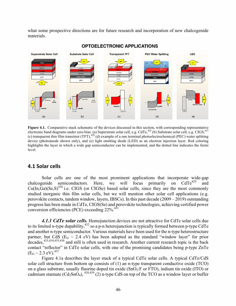
46
what some prospective directions are for future research and incorporation of new chalcogenide materials.
Figure 4.1. Comparative stack schematic of the devices discussed in this section, with corresponding representative electronic band diagrams under zero bias: (a) Superstrate solar cell, e.g. CdTe,426 (b) Substrate solar cell, e.g. CIGS,427 (c) transparent thin film transistor (TFT),428 (d) example of a one terminal photoelectrochemical (PEC) water splitting device (photoanode shown only), and (e) light emitting diode (LED) as an electron injection layer. Red coloring highlights the layer in which a wide gap semiconductor can be implemented, and the dotted line indicates the fermi level. 4.1Solarcells
Solar cells are one of the most prominent applications that incorporate wide-gap chalcogenide semiconductors. Here, we will focus primarily on CdTe429 and Cu(In,Ga)(Se,S)430 i.e. CIGS (or CIGSe) based solar cells, since they are the most commonly studied inorganic thin film solar cells, but we will mention other solar cell applications (e.g. perovskite contacts, tandem window, layers, IBSCs). In this past decade (2009 – 2019) outstanding progress has been made in CdTe, CIGS(Se) and perovskite technologies, achieving certified power conversion efficiencies (PCE) exceeding 22%.431
4.1.1 CdTe solar cells. Homojunction devices are not attractive for CdTe solar cells due
to its limited n-type dupability,432 so a p-n heterojunction is typically formed between p-type CdTe and another n-type semiconductor. Various materials have been used for the n-type heterostructure partner, but CdS (EG ~ 2.4 eV) has been adopted as the standard “window layer” for prior decades,433,434,435,436 and still is often used in research. Another current research topic is the back contact “reflector” in CdTe solar cells, with one of the promising candidates being p-type ZnTe (EG ~ 2.3 eV).437
Figure 4.1a describes the layer stack of a typical CdTe solar cells. A typical CdTe/CdS solar cell structure from bottom up consists of (1) an n-type transparent conductive oxide (TCO) on a glass substrate, usually fluorine doped tin oxide (SnO2:F or FTO), indium tin oxide (ITO) or cadmium stannate (Cd2SnO4), 438,439 (2) n-type CdS on top of the TCO as a window layer or buffer
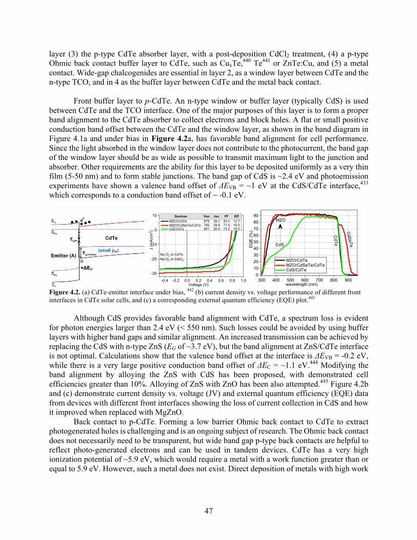
47
layer (3) the p-type CdTe absorber layer, with a post-deposition CdCl2 treatment, (4) a p-type Ohmic back contact buffer layer to CdTe, such as CuxTe,440 Te441 or ZnTe:Cu, and (5) a metal contact. Wide-gap chalcogenides are essential in layer 2, as a window layer between CdTe and the n-type TCO, and in 4 as the buffer layer between CdTe and the metal back contact.
Front buffer layer to p-CdTe. An n-type window or buffer layer (typically CdS) is used
between CdTe and the TCO interface. One of the major purposes of this layer is to form a proper band alignment to the CdTe absorber to collect electrons and block holes. A flat or small positive conduction band offset between the CdTe and the window layer, as shown in the band diagram in Figure 4.1a and under bias in Figure 4.2a, has favorable band alignment for cell performance. Since the light absorbed in the window layer does not contribute to the photocurrent, the band gap of the window layer should be as wide as possible to transmit maximum light to the junction and absorber. Other requirements are the ability for this layer to be deposited uniformly as a very thin film (5-50 nm) and to form stable junctions. The band gap of CdS is ~2.4 eV and photoemission experiments have shown a valence band offset of ΔEVB = ~1 eV at the CdS/CdTe interface,433 which corresponds to a conduction band offset of ~ -0.1 eV.
Figure 4.2. (a) CdTe-emitter interface under bias, 442 (b) current density vs. voltage performance of different front interfaces in CdTe solar cells, and (c) a corresponding external quantum efficiency (EQE) plot.443
Although CdS provides favorable band alignment with CdTe, a spectrum loss is evident
for photon energies larger than 2.4 eV (< 550 nm). Such losses could be avoided by using buffer layers with higher band gaps and similar alignment. An increased transmission can be achieved by replacing the CdS with n-type ZnS (EG of ~3.7 eV), but the band alignment at ZnS/CdTe interface is not optimal. Calculations show that the valence band offset at the interface is ΔEVB = -0.2 eV, while there is a very large positive conduction band offset of ΔEC = ~1.1 eV.444 Modifying the band alignment by alloying the ZnS with CdS has been proposed, with demonstrated cell efficiencies greater than 10%. Alloying of ZnS with ZnO has been also attempted.445 Figure 4.2b and (c) demonstrate current density vs. voltage (JV) and external quantum efficiency (EQE) data from devices with different front interfaces showing the loss of current collection in CdS and how it improved when replaced with MgZnO.
Back contact to p-CdTe. Forming a low barrier Ohmic back contact to CdTe to extract photogenerated holes is challenging and is an ongoing subject of research. The Ohmic back contact does not necessarily need to be transparent, but wide band gap p-type back contacts are helpful to reflect photo-generated electrons and can be used in tandem devices. CdTe has a very high ionization potential of ~5.9 eV, which would require a metal with a work function greater than or equal to 5.9 eV. However, such a metal does not exist. Direct deposition of metals with high work
-0.4 -0.2 0.0 0.2 0.4 0.6 0.8 1.0
-30
-20
-10
0
10
J (m
A/cm
2 )
Voltage (V)
No O2 in CdTeNo O2 in CdCl2
Devices Voc Jsc FF Eff879 26.2 55.4 12.7785 28.4 71.5 16.0847 26.6 73.2 16.5
MZO/CdTe MZO/CdSeTe/CdTe CdS/CdTe
300 400 500 600 700 800 9000
102030405060708090
EQE
(%)
wavelength (nm)
MZO/CdTe MZO/CdSeTe/CdTe CdS/CdTe
CdS
MZO
CdTe
CdSeTe
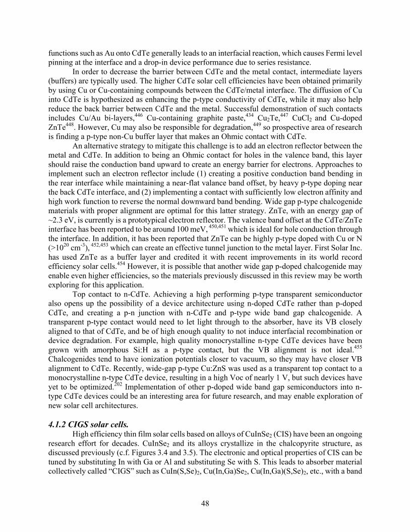
48
functions such as Au onto CdTe generally leads to an interfacial reaction, which causes Fermi level pinning at the interface and a drop-in device performance due to series resistance.
In order to decrease the barrier between CdTe and the metal contact, intermediate layers (buffers) are typically used. The higher CdTe solar cell efficiencies have been obtained primarily by using Cu or Cu-containing compounds between the CdTe/metal interface. The diffusion of Cu into CdTe is hypothesized as enhancing the p-type conductivity of CdTe, while it may also help reduce the back barrier between CdTe and the metal. Successful demonstration of such contacts includes Cu/Au bi-layers,446 Cu-containing graphite paste,434 Cu2Te,447 CuCl2 and Cu-doped ZnTe448. However, Cu may also be responsible for degradation,449 so prospective area of research is finding a p-type non-Cu buffer layer that makes an Ohmic contact with CdTe.
An alternative strategy to mitigate this challenge is to add an electron reflector between the metal and CdTe. In addition to being an Ohmic contact for holes in the valence band, this layer should raise the conduction band upward to create an energy barrier for electrons. Approaches to implement such an electron reflector include (1) creating a positive conduction band bending in the rear interface while maintaining a near-flat valance band offset, by heavy p-type doping near the back CdTe interface, and (2) implementing a contact with sufficiently low electron affinity and high work function to reverse the normal downward band bending. Wide gap p-type chalcogenide materials with proper alignment are optimal for this latter strategy. ZnTe, with an energy gap of ~2.3 eV, is currently is a prototypical electron reflector. The valence band offset at the CdTe/ZnTe interface has been reported to be around 100 meV, 450,451 which is ideal for hole conduction through the interface. In addition, it has been reported that ZnTe can be highly p-type doped with Cu or N (>1020 cm-3), 452,453 which can create an effective tunnel junction to the metal layer. First Solar Inc. has used ZnTe as a buffer layer and credited it with recent improvements in its world record efficiency solar cells.454 However, it is possible that another wide gap p-doped chalcogenide may enable even higher efficiencies, so the materials previously discussed in this review may be worth exploring for this application.
Top contact to n-CdTe. Achieving a high performing p-type transparent semiconductor also opens up the possibility of a device architecture using n-doped CdTe rather than p-doped CdTe, and creating a p-n junction with n-CdTe and p-type wide band gap chalcogenide. A transparent p-type contact would need to let light through to the absorber, have its VB closely aligned to that of CdTe, and be of high enough quality to not induce interfacial recombination or device degradation. For example, high quality monocrystalline n-type CdTe devices have been grown with amorphous Si:H as a p-type contact, but the VB alignment is not ideal.455 Chalcogenides tend to have ionization potentials closer to vacuum, so they may have closer VB alignment to CdTe. Recently, wide-gap p-type Cu:ZnS was used as a transparent top contact to a monocrystalline n-type CdTe device, resulting in a high Voc of nearly 1 V, but such devices have yet to be optimized.202 Implementation of other p-doped wide band gap semiconductors into n-type CdTe devices could be an interesting area for future research, and may enable exploration of new solar cell architectures.
4.1.2 CIGS solar cells.
High efficiency thin film solar cells based on alloys of CuInSe2 (CIS) have been an ongoing research effort for decades. CuInSe2 and its alloys crystallize in the chalcopyrite structure, as discussed previously (c.f. Figures 3.4 and 3.5). The electronic and optical properties of CIS can be tuned by substituting In with Ga or Al and substituting Se with S. This leads to absorber material collectively called “CIGS” such as CuIn(S,Se)2, Cu(In,Ga)Se2, Cu(In,Ga)(S,Se)2, etc., with a band
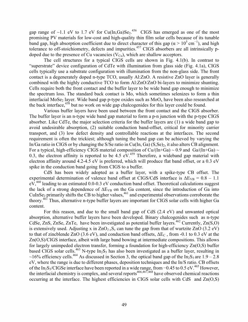
49
gap range of ~1.1 eV to 1.7 eV for Cu(In,Ga)Se2.456 CIGS has emerged as one of the most promising PV materials for low-cost and high-quality thin film solar cells because of its tunable band gap, high absorption coefficient due to direct character of this gap (α > 105 cm−1), and high tolerance to off-stoichiometry, defects and impurities.457 CIGS absorbers are all intrinsically p-doped due to the presence of Cu vacancies (VCu), which are shallow acceptors.
The cell structures for a typical CIGS cells are shown in Fig. 4.1(b). In contrast to “superstrate” device configuration of CdTe with illumination from glass side (Fig. 4.1a), CIGS cells typically use a substrate configuration with illumination from the non-glass side. The front contact is a degenerately doped n-type TCO, usually Al:ZnO. A resistive ZnO layer is generally combined with the highly conductive TCO to form Al:ZnO/ZnO bi-layers to minimize shunting. Cells require both the front contact and the buffer layer to be wide band gap enough to minimize the spectrum loss. The standard back contact is Mo, which sometimes selenizes to form a thin interfacial MoSe2 layer. Wide band gap p-type oxides such as MoOx have been also researched at the back interface,458 but no work on wide gap chalcogenides for this layer could be found.
Various buffer layers have been used between the front contact and the CIGS absorber. The buffer layer is an n-type wide band gap material to form a p-n junction with the p-type CIGS absorber. Like CdTe, the major selection criteria for the buffer layers are (1) a wide band gap to avoid undesirable absorption, (2) suitable conduction band-offset, critical for minority carrier transport, and (3) low defect density and controllable reactions at the interfaces. The second requirement is often the trickiest; although tuning the band gap can be achieved by varying the In/Ga ratio in CIGS or by changing the S/Se ratio in Cu(In, Ga) (S,Se)2, it also alters CB alignment. For a typical, high-efficiency CIGS material composition of Cu/(In+Ga) ~ 0.9 and Ga/(In+Ga) ~ 0.3, the electron affinity is reported to be 4.5 eV.459 Therefore, a wideband gap material with electron affinity around 4.2-4.5 eV is preferred, which will produce flat band offset, or a 0.3 eV spike in the conduction band going from CIGS to a buffer.
CdS has been widely adopted as a buffer layer, with a spike-type CB offset. The experimental determination of valence band offset at CIGS/CdS interface is ΔEVB = 0.8 – 1.1 eV,460 leading to an estimated 0.0-0.3 eV conduction band offset. Theoretical calculations suggest the lack of a strong dependence of ΔEVB on the Ga content, since the introduction of Ga into CuInSe2 primarily shifts the CB to higher values,461 and experimental observations corroborate the theory.461 Thus, alternative n-type buffer layers are important for CIGS solar cells with higher Ga content.
For this reason, and due to the small band gap of CdS (2.4 eV) and unwanted optical absorption, alternative buffer layers have been developed. Binary chalcogenides such as n-type CdSe, ZnS, ZnSe, ZnTe, have been investigated as potential buffer layers.462 Currently, Zn(S,O) is extensively used. Adjusting x in ZnO1-xSx can tune the gap from that of wurtzite ZnO (3.2 eV) to that of zincblende ZnO (3.6 eV), and conduction band offsets, ΔEC , from -0.1 to 0.3 eV at the Zn(O,S)/CIGS interface, albeit with large band bowing at intermediate compositions. This allows for largely unimpeded electron transfer, forming a foundation for high-efficiency Zn(O,S) buffer based CIGS solar cells.463 N-type In2S3 has also been investigated as a buffer layer, resulting in ~16% efficiency cells.464 As discussed in Section 3, the optical band gap of the In2S3 are 1.9 – 2.8 eV, where the range is due to different phases, deposition techniques and the In/S ratio. CB offsets of the In2S3/CIGSe interface have been reported in a wide range, from −0.45 to 0.5 eV.465 However, the interfacial chemistry is complex, and several reports466,467,468 have observed chemical reactions occurring at the interface. The highest efficiencies in CIGS solar cells with CdS and Zn(O,S)
50
buffer layers are 22.3% and 22.8%, respectively, 469 and the search for the next generation of buffer layers is still underway. Other chalcogenide materials mentioned in Section 2 have been also researched for CIGS solar cells. A thin p-type CuGaS2 layer, sandwiched between a p-type CuInS2 absorber layer and a Mo back contact, has a beneficial effect on the performance of thin-film CIGS solar cells fabricated on glass substrates.470 A thin interlayer of CuAlS2 has been also considered promising because this compound shows both high thermal stability and wide band gap. Besides CIGS, n-type and p-type wide chalcogenide materials have been researched for Cu2ZnSn(S,Se)4 solar cells (i.e. CZTS, CZTSSe), with quaternary “kesterite” crystal structures and similar material parameters as CIGS. Similar to CIGS, CdS and ZnS buffer layers have been used for CZTS solar cells.471–473 However, since CZTS devices have similar interfacial properties but lower efficiency than CIGS, this review does not go into detail and instead refers the reader to other references.474 4.1.3 Additional PV applications
An ongoing field of research in silicon heterojunction photovoltaics is the development of hole-selective contacts to Si to replace traditional homojunctions formed by diffusion doping.475 An example of such device is a heterojunction between amorphous Si and crystalline Si in HIT cells (“heterojunction with intrinsic thin layer”). Wide gap p-type transition metal oxides such as MoOx and WO3 have been reported as hole-selective contacts with high VOC, and transparent graphene and carbon nanotubes have been investigated as well.476,477 This is another space where implementation of a wide-gap chalcogenide-based semiconductor with sufficient alignment to the Si valence band could be fruitful, so long as passivation of the absorber is maintained. For example, it was recently demonstrated by that nanocomposites of ZnS:CuxS could be used as a hole-selective contact to n-type Si, and proof-of-concept devices were fabricated with VOC up to 535 mV and JSC of 21 mA/cm2, using 1 sun illumination.478 There also may be applications for contacts in bifacial Si solar cells.
Hybrid organic-inorganic halide perovskite solar cells, based on CH3NH3PbI3 (MAPI) and related absorbers, have gained huge prominence in the last decade, but there are still many major engineering challenges to be solved. The challenge of relevance to this review article is finding a high performing hole transport layer (HTL or HTM).479 Typically, polymer materials such as Spiro-OMeTAD have been used for this layer, but their conductivities are very low, and finding optimal replacements is an active area of research. Wide gap chalcogenides could serve as this layer due to their high mobilities and adequate band alignment. As shown in Figure 4.3a and 4.3b, CuSCN is a common material used as an HTM in both perovskite solar cells and dye sensitized solar cells (DSSC).328,480,481 Kesterite Cu2ZnSnS4 has been also applied as an HTM to perovskite solar cells.482 An additional criteria would be to function dually as a capping layer to protect the perovskite absorber from degradation under ambient atmosphere and heating, so materials with high stability are preferable for this application. CuSCN has been shown to be more thermally stable than the classic Spiro HTM (c.f. Figure 4.3c).483
51
Figure 4.3. CuSCN as a wide gap mixed anion chalcogenide in a perovskite solar cell. (a) Band alignment in a perovskite solar cell, demonstrating the adequate valence band position of CuSCN with respect to CH3NH3PBI3,484 (b) TEM interface image from Arora et al.,480 and (c) reduced thermal degradation of cells using CuSCN, compared to Spiro-OMeTAD, from Jung et al.483
Tandem or multijunction photovoltaics consist of two stacked solar cells that selectively absorb different sections of the solar spectrum.485 In order to make contact between the two layers, these devices require a tunnel p-n junction in between the two cells that can selectively transport current but let enough light through to be absorbed by the bottom cell. N-type TCOs are currently used in this application, and development of an adequate p-type transparent conductor would have important implications. This is another area where a wide gap p-type chalcogenide could be useful.
Intermediate band solar cells (IBSC) is a creative approach to achieve efficiencies beyond the Shockley-Queissar limit.486 Rather than optimizing the fundamental band gap for solar absorption, IBSCs intentionally introduce a deep level, mid-gap defect such that absorption occurs at two different wavelengths, from the CB to the deep level and from the deep level to the VB.255 Wide gap chalcopyrite chalcogenides have been explored as the absorbers for IBSC due to their wide, direct gap, and their ease of dopability. There have been investigations on possible IBSC dopants in chalcopyrites CuAlS2, CuGaS2, AgGaSe2, AgGaT2,256,262,487 but very few device related publications could be found in literature. 4.2OtherDevices 4.2.1Transparentthinfilmtransistors Transparent thin film transistors (TFTs) require wide band gap semiconductors as the active/channel layer to ensure the visible range transparency of the devices. Another advantage of wide band gap semiconductors for TFT applications is that their intrinsic carrier concentrations tend to be lower than for narrow band gap materials (since the former are more difficult to dope) thus achieving low “off” current. One more advantage is that the wider band gap results in a larger band offset, leading to better control of the carrier concentrations by the gate voltage. Simultaneously, high electronic quality of the channel’s interfaces with the insulator is generally required to maintain high carrier mobilities without scattering on interfacial defects. Thus, wide band gap semiconductors with high mobility but low carrier concentrations are suitable as the active layer in transparent TFTs. N-type oxides such as amorphous In-Ga-Zn-O (IGZO) meet these requirements and are the conventional choice of channel layer material in unipolar switching
52
devices. On the other hand, chalcogenide wide band gap semiconductors may enable bipolar devices, complementary metal oxide semiconductor (CMOS) technology and transparent circuits, since they have better propensity for p-type doping the oxides.
Figure 4.1c shows a typical schematic of a thin film transistor and its band alignment under no bias. The source electrode is grounded, a fixed voltage bias is applied to drain electrode, and the gate voltage Vg is used to control the carrier concentration in the channel, e.g. the current between source and drain. For example, in an n-type TFT when Vg is above the threshold voltage Vth, the channel layer CBM bends down and is closer to the Fermi level, leading to a higher concentration near the insulator/channel layer interface, called the “on” state. In contrast, if Vg is lower than Vth, the CBM bends upwards and causes a lower carrier concentration, i.e. the “off” state. Thus, the current between source and drain, IDS, shows a clear on-off switching as a function of Vg. IDS from p-type TFT changes inversely compared to n-type TFT (Figure 4.4). There are several p-type oxides used as TFT channels, mainly based on CuO, SnO, et al.7 But their performance is not as good as for their n-type counterparts, probably due the low hole mobility originated from the localized oxygen 2p orbitals. By introducing a chalcogen, more covalent bonds are formed between cations and anions and a higher mobility is expected, which may lead to better performance. There have only been a few reported attempts to implement chalcogenides into transistors, and their high achieved mobilities offer inspiration to continue to explore other this material space. For example, the fabrication of an n-type SnS2-xSex TFT by spin coating resulted in an n-type mobility greater than 10 cm2
V-1 s-1, comparable to the mobility of IGZO based TFTs (~20 cm2
V-
1 s-1).488,489 TFTs using p-type ZnTe as the channel layer were first reported as far back as 1967,
with mobilities of 1—10 cm2 V-1
s-1. 490 Later p-type ZnTe TFT was prepared again and integrated with n-type ZnO TFTs to form a complementary logic circuit, but the low on-current limited the on/off ratio to only ~100.491 N-type CdS TFTs have also been reported to function in both accumulation and depletion mode, with a mobility of 1.25 cm2
V-1 s-1.492 CdS is promising due to its high mobility >100 cm2
V-1
s-1and its low temperature processing for flexible electronics.493 Additionally, n-type CdSe was reported decades ago with a mobility of 4-30 cm2
V-1 s-1.494 P-type PbS TFTs have been prepared
chemically, with low mobility in as-deposited devices but improvement after thermal annealing.495,496 We note that channel layers are not limited to wide band gap semiconductors. For example TFTs using narrower band gap (<2 eV) semiconductors as channel layers have been reported, e.g. CuInTe2.497

53
Figure 4.4. Example transfer curves of (a) an n-type TFT (IGZO, reproduced from reference),498 and (b) a p-type TFT (SnO, reproduced from reference).499 4.2.2Watersplittingphotocatalystsandphoto-electrocatalysts
Wide band gap (WBG) chalcogenides have suitable properties for applications in both two types of water splitting mechanisms – as photocatalysts for photocatalytic (PC) devices and as photo-electrocatalysts for photoelectrochemical (PEC) devices – and have been extensively investigated.
Photocatalysts. Due to relatively high CB positions compared to oxides, wide band gap chalcogenides are attractive choices as photocatalysts for ‘overall water splitting.’ The three fundamental criteria of photocatalyst material for H2 generation by water splitting are suitable band alignment, optimal band gap, and resistance to corrosion in electrolyte solution. In particular, the conduction band minimum (CBM) potential must be lower than 0 V vs. normal hydrogen electrode (NHE) to reduce water, and the valence band minimum (VBM) potential must be higher than 1.23 V vs. NHE to oxidize water. Although the difference between water reduction and oxidation potentials is only 1.23 eV, for a single material semiconductor photoelectrode the band gap must lie within the range of 1.6 < EG < 2.4 eV;500 due to the required overpotential to drive the hydrogen evolution reaction (HER) and oxygen evolution reaction (OER) at the same time, as well as to account for different loss mechanisms in practical devices. Other desirable properties are high carrier mobility to enhance charge transfer, and good electron and hole mobilities to increase charge separation and to reduce recombination. A trade-off between crystallinity and active surface area is also of interest, as a higher degree of crystallinity improves charge transport while a nanoporous or amorphous structure provides more active sites for catalysis.
Multinary metal chalcogenides such as ZnS-CuInS2, CuGaS2–ZnS, ZnIn2S4 and NaInS2 have been explored in search of improved photocatalytic properties in the visible spectrum.501–504 For a visible light driven hydrogen evolution reaction, the band gaps of ZnS, CuGaS2 and AgGaS2 are too wide to absorb enough light. For CuInS2 and AgInS2, the conduction band potential is too low. Alloyed WBG chalcogenides with optimized compositions (e.g. CuIn0.3Ga0.7S2 and AgIn0.1Ga0.9S2) can balance the optimal properties of band gap and CB alignment and tune them to desirable levels.505,506 Computational screenings have recently provided a promising avenue for searching for photocatalysts. Based on first principles analysis, Ba2ZnSe3, with a band gap of 2.75
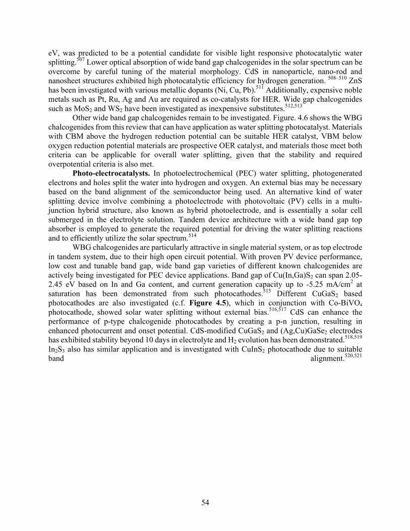
54
eV, was predicted to be a potential candidate for visible light responsive photocatalytic water splitting.507 Lower optical absorption of wide band gap chalcogenides in the solar spectrum can be overcome by careful tuning of the material morphology. CdS in nanoparticle, nano-rod and nanosheet structures exhibited high photocatalytic efficiency for hydrogen generation. 508–510 ZnS has been investigated with various metallic dopants (Ni, Cu, Pb).511 Additionally, expensive noble metals such as Pt, Ru, Ag and Au are required as co-catalysts for HER. Wide gap chalcogenides such as MoS2 and WS2 have been investigated as inexpensive substitutes.512,513
Other wide band gap chalcogenides remain to be investigated. Figure. 4.6 shows the WBG chalcogenides from this review that can have application as water splitting photocatalyst. Materials with CBM above the hydrogen reduction potential can be suitable HER catalyst, VBM below oxygen reduction potential materials are prospective OER catalyst, and materials those meet both criteria can be applicable for overall water splitting, given that the stability and required overpotential criteria is also met.
Photo-electrocatalysts. In photoelectrochemical (PEC) water splitting, photogenerated electrons and holes split the water into hydrogen and oxygen. An external bias may be necessary based on the band alignment of the semiconductor being used. An alternative kind of water splitting device involve combining a photoelectrode with photovoltaic (PV) cells in a multi-junction hybrid structure, also known as hybrid photoelectrode, and is essentially a solar cell submerged in the electrolyte solution. Tandem device architecture with a wide band gap top absorber is employed to generate the required potential for driving the water splitting reactions and to efficiently utilize the solar spectrum.514 WBG chalcogenides are particularly attractive in single material system, or as top electrode in tandem system, due to their high open circuit potential. With proven PV device performance, low cost and tunable band gap, wide band gap varieties of different known chalcogenides are actively being investigated for PEC device applications. Band gap of Cu(In,Ga)S2 can span 2.05-2.45 eV based on In and Ga content, and current generation capacity up to -5.25 mA/cm2 at saturation has been demonstrated from such photocathodes.515 Different CuGaS2 based photocathodes are also investigated (c.f. Figure 4.5), which in conjunction with Co-BiVO4 photocathode, showed solar water splitting without external bias.516,517 CdS can enhance the performance of p-type chalcogenide photocathodes by creating a p-n junction, resulting in enhanced photocurrent and onset potential. CdS-modified CuGaS2 and (Ag,Cu)GaSe2 electrodes has exhibited stability beyond 10 days in electrolyte and H2 evolution has been demonstrated.518,519 In2S3 also has similar application and is investigated with CuInS2 photocathode due to suitable band alignment.520,521
55
Figure 4.5. (a) Photocatalytic H2 production from CuGaS2–ZnS nano-heterostructure under visible light irradiation; reproduced from reference.502 (b) Photoelectrochemical H2 evolution from a Pt/CdS/CuGaSe2 electrode (0.09 cm2) under 300W Xe lamp with an electrode potential of -0.1V RHE; reproduced from reference.518
4.2.3Diodes Light emitting diodes (LEDs) allow for direct conversion of electrical energy to light. A simple device structure is depicted in Figure 4.1e. Holes and electrons are injected via the hole transport and electron injection layer, respectively, and combine in the active layer to emit light. Some wide band gap chalcogenides are used in light emitting diodes (LEDs) as transport and injection layers. Their wide band gaps enable light to escape the device, maximizing the luminescence quantum efficiency. Band alignments of the transport and injection layers with the emitting layer, as well as their high conductivities, are important interface and materials properties for this application. Here, we mention some examples of wide band gap chalcogenides application in Light emitting diodes. In addition to acting as transport layers, wide gap chalogenides have been used as active layers too (e.g. ZnS, CdS, BeS, etc.). N-type CdS has been studied as an electron transport layer in LEDs by forming a heterojunction with poly p-phenylene vinylene (PPV). 522 The close band alignment between CdS and PPV, compared to that between Al and PPV, lowers the energy barrier for electron injection. Concurrently, CdS blocks holes from flowing to the negative electrode, and helps electron injection. 2D materials such as MoS2, WS2, and TaS2 have also been investigated as hole injection layers to replace contact materials in organic LED (OLED) applications, since these chalcogenides won’t cause degradation of the organic components like ITO electrodes do.523 A few p-type chalcogenides have also been deployed in LEDs as hole transport or injection layers. Hole-injection barrier formed between oxygen plasma treated LaCuOSe:Mg and NPB can be as low as 0.3 eV, approximately a half of a conventional ITO/NPB interface, indicating its potential as an efficient transparent anode for OLEDs and other organic electronic devices.524 A chemically inert interface with a hole injection barrier of 0.11 eV was formed at the interface of BaCuSeF/ZnPc (zinc phthalocyanine), probably providing improved device performance for OLEDs and OPVs compared with ITO electrodes.525 The p-type CuSCN layer can help balance the electrons and holes injection rates in n-ZnO nanorods/p-CuSCN heterojunction LEDs, enhancing efficiency of the radiative recombination.526 Besides its application in LEDs, CuSCN
56
also finds its positions in TFTs and PV cells with its wide band gap, hole-transport characteristics, and low-temperature solution-processability.527
In the past, ZnS has been heavily studied as a candidate active material for blue LEDs,528,529 but these research efforts decreased with the advent of GaN-based LEDs. More recently, core/shell nanocrystal quantum dots of CdSe-ZnS530 and CdSe-CdS531, among other systems, were also studied as efficient electroluminescent materials, to be incorporated into light emitting diodes. The good matching between CdSe nanocrystals and the metal electrode contributes a low operating voltage. The color of the emission can also be tuned by voltage due to quantum size effect.532 Single crystal p-type ZnTe can also be made into green LED together with Al.533 4.3BandOffsetsofWide-GapChalcogenidesforDevices In Section 3 we have discussed a large set of wide gap chalcogenide semiconductors that could be used for device applications, and assessed their advantages and disadvantages. However, in Section 4 we have seen that the materials used in solar cells, transparent transistors, etc., are limited to only a few candidates, primarily CdS, ZnS, ZnTe, In2S3 and SnS2. What is preventing researchers from incorporating less conventional chalcogenides into these devices as contacts or active layers? First may be simply the lack of recognition of which materials are available and what their corresponding properties are. We hope to have alleviated this barrier with the discussion of potential materials and their properties in Section 3, including a summary Figure 3.12 and tabulated values in the Supporting Information. Second, in order to select an appropriate material for a device application, it is essential to understand the alignment of the valence and conduction bands at interfaces and the types of junctions that will form. This can be a somewhat trickier constraint, as alignment changes drastically depending on environment, grain orientation, interface configuration, etc.
To help assess band alignment in current and future device applications, in Figure 4.6 we compile and tabulate the band offset positions reported in the literature for many of the wide gap chalcogenide semiconductors discussed previously (c.f. SI table for more details). When available, we have reported measurements from x-ray and ultraviolet electron spectroscopy (XPS/UPS), referenced to vacuum levels. If these have been not experimentally measured, we have reported calculated offsets and denoted these cases with a * prefix (c.f. SI table for level of theory and DFT functional used). Band offsets are arranged in increasing order of ionization potential, and color represents reported doping type in the literature. The grey materials on the right side of the graph are known absorbers in solar cell applications (CdTe, CIGS, Si, GaAs). References for all reported values are tabulated in the SI. We also note that uncertainties in XPS/UPS data are typically >0.1 eV, and that it is strictly a surface measurement. DFT alignments can vary by grain orientations considered in the model and averaging scheme, so they may not robustly represent experimental alignments. In addition to the transport properties we’ve discussed so far, these measurements are key first steps to understanding band bending and charge transport at the interfaces of the heterojunctions we have discussed in this section. The next steps are explicit interface simulations via slab supercell approaches and junction modeling, and are covered in depth elsewhere (c.f. Section 2.5.1). Ultimately experimental band alignment measurements of real interfaces is needed to assess band positions and bending. This has been performed for many of the chalcogenide interfaces discussed in Section 4,114,270,465,317,534 but not for the less heavily studied systems.
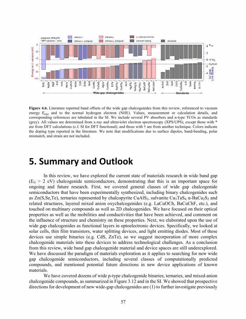
57
Figure 4.6. Literature reported band offsets of the wide gap chalcogenides from this review, referenced to vacuum energy 𝐸x#? and to the normal hydrogen electron (NHE). Values, measurement or calculation details, and corresponding references are tabulated in the SI. We include several PV absorbers and n-type TCOs as standards (grey). All values are determined from x-ray and ultraviolet electron spectroscopy (XPS/UPS), except those with * are from DFT calculations (c.f. SI for DFT functional), and those with † are from another technique. Colors indicate the doping type reported in the literature. We note that modifications due to surface dipoles, band-bending, polar mismatch, and strain are not included.
5.SummaryandOutlook In this review, we have explored the current state of materials research in wide band gap (EG > 2 eV) chalcogenide semiconductors, demonstrating that this is an important space for ongoing and future research. First, we covered general classes of wide gap chalcogenide semiconductors that have been experimentally synthesized, including binary chalcogenides such as Zn(S,Se,Te), ternaries represented by chalcopyrite CuAlS2, sulvanite Cu3TaS4, α-BaCu2S2 and related structures, layered mixed anion oxychalcogenides (e.g. LaCuOCh, BaCuChF, etc.), and touched on multinary compounds as well as 2D chalcogenides. We have focused on their optical properties as well as the mobilities and conductivities that have been achieved, and comment on the influence of structure and chemistry on these properties. Next, we elaborated upon the use of wide gap chalcogenides as functional layers in optoelectronic devices. Specifically, we looked at solar cells, thin film transistors, water splitting devices, and light emitting diodes. Most of these devices use simple binaries (e.g. CdS, ZnTe), so we suggest incorporation of more complex chalcogenide materials into these devices to address technological challenges. As a conclusion from this review, wide band gap chalcogenide material and device spaces are still underexplored. We have discussed the paradigm of materials exploration as it applies to searching for new wide gap chalcogenide semiconductors, including several classes of computationally predicted compounds, and mentioned potential future directions in new device applications of known materials.
We have covered dozens of wide p-type chalcogenide binaries, ternaries, and mixed-anion chalcogenide compounds, as summarized in Figure 3.12 and in the SI. We showed that prospective directions for development of new wide-gap chalcogenides are (1) to further investigate previously
58
synthesized materials in databases for their properties, (2) look towards chemical counterparts (e.g. chalcogenide delafossites or perovskites) to find new materials, or (3) to propose new stoichiometries and chemistries altogether (e.g. Cs2Zn3Se4). These general directions provide a groundwork for further computational and experimental investigation. As noted, only a portion of these materials have been calculated to be p-type dopable, only a fraction of those have specific dopants proposed, and even fewer have been synthesized with proposed dopants. As mentioned previously, now are tools available (e.g. PyCDT, PyLADA) to implement defect calculations in every high throughput computational screening study in order to better understand dopability. In addition to further studies of dopability, defects, and synthesizability, it is also important to consider the band offsets and alignment of these materials to justify their use and pairing in optoelectronic devices. What are some next steps that can be taken in the field? First, we suggest continued research into combining known compounds with complementary properties to tune desired functionality. This involves continued investigation into anion and cation alloying in the materials discussed in this paper (e.g. Cd1-xZnxS, CuxAg1-xAlS2, LaCuOS1-xSex), and in others we have yet to discover. As shown in this review, as well as in the n-type TCO literature, many material breakthroughs have originated from tuning properties in solid solutions and alloys. In addition, exploring composite material systems (e.g. CuyS:ZnS, Section 2.1) and using “δ-doping” (e.g. ZnCh system, Section 2.1) to combine different systems could leverage the desired properties of each subsystem. Second, this review inspires clever engineering of known chalcogenide compounds. This involves using new processing techniques, non-equilibrium synthesis methods, post-processing, etc., to promote carrier transport and high doping in chalcogenide host materials. Additionally, the community can learn from e.g. CuSCN how to engineer similar quasi-molecular structures where the valence band is more disperse than the conduction band, and explore band engineering by thinning materials to tune band gaps and mobilities (c.f. Section 2.6). Both of these suggested approaches are inspired by the progress so far in the wide gap chalcogenide community, as discussed in this review.
Future research in the field will also undoubtedly involve exploration of new chalcogenide compounds and dopants, both 3D and 2D structures, using a variety of strategies. As discussed, new chalcogenides can be explored computationally and experimentally by taking structural analogs of oxides or other counterparts (e.g. chalcogenide delafossites or perovskites, c.f. Sections 3.4.3 and 3.4.4). To this end, the synthesis and characterization of computationally predicted wide gap conducting p-type materials (e.g. ZrOS, Cs2Zn3Se4, etc.) would be important. Specifically, this review has highlighted continued high throughput searches for new Cu-free p-type systems and Cd-free n-type systems for device applications (c.f. Section 4). Defect calculations and corresponding doping experiments will be essential to understand new dopants in these systems of interest. (4)
Finally, this review motivates continued investigation of interfaces of wide band gap chalcogenides and their device applications. Developing a theoretical understanding of stability, degradation and interface modeling in chalcogenides is essential to deciding which can be used in devices. In particular, the band alignment of many of the systems we have discussed remains to be understood, and such understanding is critical to tailoring to a particular device. Experimentally, this can be realized by synthesis of interfacial heterostructures and measurement of their interfacial band offsets. Incorporation of both n-type and p-type chalcogenide materials into existing devices as well as designing new device architectures using these unique materials, has potential to lead to significantly higher performances and efficiencies. Together, this suite of future advances into
59
wide band gap chalcogenide materials and devices could be a key component in accelerating society’s renewable energy transformation and enabling other technological advances.
Acknowledgements
This work was authored in part by the National Renewable Energy Laboratory, operated by Alliance for Sustainable Energy, LLC, for the U.S. Department of Energy (DOE) under Contract No. DE-AC36-08GO28308. Funding provided by U.S. Department of Energy, Office of Science, Basic Energy Sciences, as part of an Energy Frontier Research Center “Center for Next Generation Materials by Design (CNGMD)”. Y.H. acknowledges his stipend from China Scholarship Council, and in particular thanks Yan Wang for her inspiration and discussion. R.W.R. acknowledges her Ph.D. funding from the UC Berkeley Chancellor’s Fellowship and the National Science Foundation (NSF) Graduate Research Fellowship Program (GRFP) under Grant Numbers DGE1106400 and DGE1752814. The views expressed in the article do not necessarily represent the views of the DOE or the U.S. Government.
AuthorContributions A.Z, Y.H., and R.W.R. conceptualized the review and edited the manuscript. Y.H. and R.W.R. co-wrote Section 2 and Sections 3.1-3.5. R.W.R. wrote Section 1, Section 4.3, Section 5, and introductions to all sections. H.Z. wrote Section 3.6. T.A. and R.W.R. wrote Section 4.1. Y.H. wrote section 4.2.1 and 4.2.3. I.K. wrote section 4.2.2. A.Z. and K.P. supervised the work.
References (1) Wager,J.F.;Keszler,D.A.;Presley,R.E.TransparentElectronics;2010.(2) Minami,T.TransparentConductingOxideSemiconductorsforTransparentElectrodes.
Semicond.Sci.Technol.2005,20(4).(3) Rakhshani,A.E.;Makdisi,Y.;Ramazaniyan,H.A.ElectronicandOpticalPropertiesof
Fluorine-DopedTinOxideFilms.J.Appl.Phys.1998,83(2).(4) Jiang,X.;Wong,F.L.;Fung,M.K.;Lee,S.T.Aluminum-DopedZincOxideFilmsas
TransparentConductiveElectrodeforOrganicLight-EmittingDevices.Appl.Phys.Lett.2003,83(9),1875–1877.
(5) Nomura,K.;Ohta,H.;Takagi,A.;Kamiya,T.;Hirano,M.;Hosono,H.Room-TemperatureFabricationofTransparentFlexibleThin-FilmTransistorsUsingAmorphousOxideSemiconductors.Nature2004,432(7016),488–492.
(6) Kawazoe,H.;Yasukawa,M.;Hyodo,H.P-TypeElectricalConductioninTransparentThin
60
FilmsofCuAlO2.Nature1997,289,939–942.(7) Wang,Z.;Nayak,P.K.;Caraveo-Frescas,J.A.;Alshareef,H.N.RecentDevelopmentsinP-
TypeOxideSemiconductorMaterialsandDevices.Adv.Mater.2016,28(20),3831–3892.(8) Cheng,J.;Fan,D.;Wang,H.;Liu,B.;Zhang,Y.;Yan,H.ChemicalBathDepositionof
CrystallineZnSThinFilms.Semicond.Sci.Technol.2003,18(7),676–679.(9) Choi,J.Y.;Kim,K.-J.;Yoo,J.-B.;Kim,D.PropertiesofCadmiumSulfideThinFilms
DepositedbyChemicalBathDepositionwithUltrasonication.Sol.Energy1998,64(1–3),41–47.
(10) Gordillo,J.A.R.G.StudyofElectriclaPropertiesinZnxCd1-XSThinFilms.Sol.EnergyMater.1989,19,421–431.
(11) Liu,M.;Wang,Y.;Huang,F.OpticalandElectricalPropertiesStudyonP-TypeConductingCuAlS2+xwithWideBandGap.2007,57,1133–1136.
(12) Han,Y.;Siol,S.;Zhang,Q.;Zakutayev,A.OptoelectronicPropertiesofStrontiumandBariumCopperSulfidesPreparedbyCombinatorialSputtering.Chem.Mater.2017,29(19),8239–8248.
(13) Newhouse,P.F.;Hersh,P.A.;Zakutayev,A.;Richard,A.;Platt,H.A.S.;Keszler,D.A.;Tate,J.ThinFilmPreparationandCharacterizationofWideBandGapCu3TaQ4(Q=SorSe)p-TypeSemiconductors.ThinSolidFilms2009,517(7),2473–2476.
(14) Hiramatsu,H.;Kamioka,H.;Ueda,K.;Ohta,H.;Kamiya,T.;Hirano,M.;Hosono,H.Opto-ElectronicPropertiesandLight-EmittingDeviceApplicationofWidegapLayeredOxychalcogenides:LaCuOCh(Ch=Chalcogen)andLa2CdO2Se2.Phys.StatusSolidiAppl.Mater.Sci.2006,203(11),2800–2811.
(15) Hatch,S.M.;Briscoe,J.;Dunn,S.ASelf-PoweredZnO-Nanorod/CuSCNUVPhotodetectorExhibitingRapidResponse.Adv.Mater.2013,25(6),867–871.
(16) Kim,K.S.;Zhao,Y.;Jang,H.;Lee,S.Y.;Kim,J.M.;Kim,K.S.;Ahn,J.H.;Kim,P.;Choi,J.Y.;Hong,B.H.Large-ScalePatternGrowthofGrapheneFilmsforStretchableTransparentElectrodes.Nature2009,457(7230),706–710.
(17) Che,Y.;Chen,H.;Gui,H.;Liu,J.;Liu,B.;Zhou,C.ReviewofCarbonNanotubeNanoelectronicsandMacroelectronics.Semicond.Sci.Technol.2014,29(7).
(18) Casady,J.B.;Johnson,R.W.StatusofSiliconCarbide(SiC)asaWide-BandgapSemiconductorforHigh-TemperatureApplications:AReview.InHigh-TemperatureElectronics;1998.
(19) Mohammad,S.N.;Salvador,A.A.;Morkoç,H.EmergingGalliumNitrideBasedDevices.Proc.IEEE1995.
(20) Rajan,S.;Jena,D.GalliumNitrideElectronics.SemiconductorScienceandTechnology.2013.
(21) Aperathitis,E.;Kambilafka,V.;Modreanu,M.PropertiesofN-TypeZnNThinFilmsasChannelforTransparentThinFilmTransistors.ThinSolidFilms2009,518(4),1036–1039.
(22) Grundmann,M.;Schein,F.L.;Lorenz,M.;Böntgen,T.;Lenzner,J.;VonWenckstern,H.CuprousIodide-Ap-TypeTransparentSemiconductor:HistoryandNovelApplications.Phys.StatusSolidiAppl.Mater.Sci.2013,210(9),1671–1703.
(23) Takahashi,K.;Yoshikawa,A.;Sandhu,A.WideBandgapSemiconductors;2007;Vol.10.(24) Zhang,K.H.L.;Xi,K.;Blamire,M.G.;Egdell,R.G.P-TypeTransparentConductingOxides.
J.Phys.Condens.Matter2016,28(38),383002.
61
(25) Delahoy,A.E.;Guo,S.TransparentConductingOxidesforPhotovoltaics.InHandbookofPhotovoltaicScienceandEngineering;Luque,A.,Hegedus,S.,Eds.;JohnWiley&Sons,Ltd.,2011;pp716–796.
(26) Morko,H.HandbookofNitrideSemiconductorsandDevices;2008.(27) Pierson,H.O.HandbookofRefractoryCarbidesandNitrides :Properties,Characteristics,
Processing,andApplications.Handb.Refract.CarbidesNitrides1996.(28) Allen,M.J.;Tung,V.C.;Kaner,R.B.HoneycombCarbon:AReviewofGraphene.Chem.
Rev.2009,110(1),132–145.(29) Ruda,H.E.WidegapII–VICompoundsforOpto-ElectronicApplications;Ruda,H.E.,Ed.;
SpringerScience&BusinessMedia,2013.(30) Tate,J.;Ju,H.L.;Moon,J.C.;Zakutayev,A.;Richard,A.P.;Russell,J.;McIntyre,D.H.
OriginofP-TypeConductioninSingle-CrystalCuAlO2.Phys.Rev.B2009,80(16),165206.(31) Huang,F.;Liu,M.;Yang,C.HighlyEnhancedp-TypeElectricalConductioninWideBand
Gap.Sol.EnergyMater.Sol.Cells2011,95(10),2924–2927.(32) Hiramatsu,H.;Ueda,K.;Ohta,H.;Hirano,M.;Kamiya,T.;Hosono,H.DegenerateP-Type
ConductivityinWide-GapLaCuOS1xSex(X=0-1)EpitaxialFilms.Appl.Phys.Lett.2003,82(7),1048–1050.
(33) Zunger,A.PracticalDopingPrinciples.Appl.Phys.Lett.2003,83(1),57.(34) Chan,M.K.Y.;Ceder,G.EfficientBandGapPredictionforSolids.Phys.Rev.Lett.2010,
105(19),196403.(35) Sun,W.;Bartel,C.J.;Arca,E.;Bauers,S.R.;Matthews,B.;Orvañanos,B.;Chen,B.R.;
Toney,M.F.;Schelhas,L.T.;Tumas,W.;etal.AMapoftheInorganicTernaryMetalNitrides.Nat.Mater.2019.
(36) Bauers,S.R.;Holder,A.;Sun,W.;Melamed,C.L.;Woods-Robinson,R.;Mangum,J.;Perkins,J.;Tumas,W.;Gorman,B.;Tamboli,A.;etal.TernaryNitrideSemiconductorsintheRocksaltCrystalStructure.Proc.Natl.Acad.Sci.2019,201904926.
(37) Han,Y.;Holder,A.M.;Siol,S.;Lany,S.;Zhang,Q.;Zakutayev,A.Zinc-StabilizedManganeseTelluridewithWurtziteCrystalStructure.J.Phys.Chem.C2018,122(32),18769–18775.
(38) Bureau,B.;Zhang,X.H.;Smektala,F.;Adam,J.L.;Troles,J.;Ma,H.L.;Boussard-Plèdel,C.;Lucas,J.;Lucas,P.;LeCoq,D.;etal.RecentAdvancesinChalcogenideGlasses.J.Non.Cryst.Solids2004,345,276–283.
(39) Zakery,A.;Elliott,S.R.OpticalPropertiesandApplicationsofChalcogenideGlasses:AReview.J.Non.Cryst.Solids2003,330(1–3),1–12.
(40) Jain,A.;Ong,S.P.;Hautier,G.;Chen,W.;Richards,W.D.;Dacek,S.;Cholia,S.;Gunter,D.;Skinner,D.;Ceder,G.;etal.Commentary:TheMaterialsProject:AMaterialsGenomeApproachtoAcceleratingMaterialsInnovation.APLMater.2013,1(1),011002.
(41) Curtarolo,S.;Setyawan,W.;Wang,S.;Xue,J.;Yang,K.;Taylor,R.H.;Nelson,L.J.;Hart,G.L.W.;Sanvito,S.;Buongiorno-Nardelli,M.;etal.AFLOWLIB.ORG:ADistributedMaterialsPropertiesRepositoryfromHigh-ThroughputAbInitioCalculations.Comput.Mater.Sci.2012,58,227–235.
(42) Lany,S.Band-StructureCalculationsforthe3dTransitionMetalOxidesinGW.Phys.Rev.B2013,87(8),085112.
(43) Lany,S.SemiconductingTransitionMetalOxides.J.Phys.Condens.Matter2015,27(28),
62
283203.(44) Stevanović,V.;Lany,S.;Zhang,X.;Zunger,A.CorrectingDensityFunctionalTheoryfor
AccuratePredictionsofCompoundEnthalpiesofFormation:FittedElemental-PhaseReferenceEnergies.Phys.Rev.B2012,85(11),115104.
(45) Kirklin,S.;Saal,J.E.;Meredig,B.;Thompson,A.;Doak,J.W.;Aykol,M.;Rühl,S.;Wolverton,C.TheOpenQuantumMaterialsDatabase(OQMD):AssessingtheAccuracyofDFTFormationEnergies.npjComput.Mater.2015,1.
(46) Woods-Robinson,R.;Broberg,D.;Faghaninia,A.;Jain,A.;Dwaraknath,S.S.;Persson,K.A.AssessingHigh-ThroughputDescriptorsforPredictionofTransparentConductors.Chem.Mater.2018,30(22),8375–8389.
(47) Hautier,G.;Ong,S.P.;Jain,A.;Moore,C.J.;Ceder,G.AccuracyofDensityFunctionalTheoryinPredictingFormationEnergiesofTernaryOxidesfromBinaryOxidesandItsImplicationonPhaseStability.Phys.Rev.B-Condens.MatterMater.Phys.2012,85(15).
(48) Aykol,M.;Dwaraknath,S.S.;Sun,W.;Persson,K.A.ThermodynamicLimitforSynthesisofMetastableInorganicMaterials.Sci.Adv.2018,4(4),1–8.
(49) Singh,A.K.;Zhou,L.;Shinde,A.;Suram,S.K.;Montoya,J.H.;Winston,D.;Gregoire,J.M.;Persson,K.A.ElectrochemicalStabilityofMetastableMaterials.Chem.Mater.2017,29,10159−10167.
(50) Nian,H.;Hahn,S.H.;Koo,K.-K.;Shin,E.W.;Kim,E.J.Sol–GelDerivedN-DopedZnOThinFilms.Mater.Lett.2009,63(26),2246–2248.
(51) Bian,J.M.;Li,X.M.;Gao,X.D.;Yu,W.D.;Chen,L.D.DepositionandElectricalPropertiesofN–InCodopedp-TypeZnOFilmsbyUltrasonicSprayPyrolysis.Appl.Phys.Lett.2004,84(4),541.
(52) Cao,Z.ThinFilmGrowth:Physics,MaterialScienceandApplications;2011.(53) Rockett,A.TheMaterialsScienceofSemiconductors;2008.(54) Seshan,K.HandbookofThinFilmDeposition.HandbookofThinFilmDeposition.2012,p
412.(55) Holloway,P.H.;Mcguire,G.E.HandbookofCompoundSemiconductors :Growth,
Processing,Characterization,andDevices(MaterialsScienceandProcessTechnologySeries).Mater.Sci.ProcessTechnol.Ser.1995,1–3.
(56) Capper,P.BulkCrystalGrowthofElectronic,OpticalandOptoelectronicMaterials;2010.(57) Rocket,A.PhysicalVaporDeposition.Mater.Sci.Semicond.2008,505–572.(58) Depla,D.;Mahieu,S.;Greene,J.E.SputterDepositionProcesses.InHandbookof
DepositionTechnologiesforFilmsandCoatings;2010;pp253–296.(59) Fujioka,H.PulsedLaserDeposition(PLD).InHandbookofCrystalGrowth;2015;pp365–
397.(60) Bishop,C.A.;Bishop,C.A.ThermalEvaporation.InVacuumDepositionOntoWebs,Films
andFoils;2015;pp301–331.(61) Bishop,C.A.ElectronBeam(E-Beam)Evaporation.InVacuumDepositionOntoWebs,
FilmsandFoils;2015;pp289–299.(62) Arthur,J.R.MolecularBeamEpitaxy.Surf.Sci.2002,500(1–3),189–217.(63) Waag,A.;Heinke,H.;Scholl,S.;Becker,C.R.;Landwehr,G.GrowthofMgTeandCd1−
XMgxTeThinFilmsbyMolecularBeamEpitaxy.J.Cryst.Growth1993,131(3–4),607–611.
63
(64) Ritala,M.;Niinisto,J.AtomicLayerDeposition¨.InChemicalVaporDeposition;2009;pp158–206.
(65) Pakkala,A.;Putkonen,M.AtomicLayerDeposition.InHandbookofDepositionTechnologiesforFilmsandCoatings;2010;pp364–391.
(66) Thompson,A.G.MOCVDTechnologyforSemiconductors.Mater.Lett.1997,30(4),255–263.
(67) Reif,R.;Kern,W.Plasma-EnhancedChemicalVaporDeposition.InThinFilmProcessesII;2012;pp525–564.
(68) KoppAlves,A.;Bergmann,C.P.;Berutti,F.A.SprayPyrolysis.InNovelSynthesisandCharacterizationofNanostructuredMaterials;2013;pp23–30.
(69) Hench,L.L.;West,J.K.TheSol-GelProcess.Chem.Rev.1990,90(1),33–72.(70) Levy,D.;Zayat,M.TheSol-GelHandbook;2015;Vol.1–3.(71) DeGuire,M.R.;Bauermann,L.P.;Parikh,H.;Bill,J.ChemicalBathDeposition.In
ChemicalSolutionDepositionofFunctionalOxideThinFilms;2013;Vol.9783211993,pp319–339.
(72) Goushi,Y.;Hakuma,H.;Tabuchi,K.;Kijima,S.;Kushiya,K.FabricationofPentanaryCu(InGa)(SeS)2AbsorbersbySelenizationandSulfurization.Sol.EnergyMater.Sol.Cells2009,93(8),1318–1320.
(73) Fiory,A.T.MethodsinRapidThermalAnnealing.InProceedingsofRTP2000;2000;pp15–25.
(74) Lüdge,A.;Riemann,H.;Wünscher,M.;Behr,G.;Löser,W.;Muiznieks,A.;Cröll,A.FloatingZoneCrystalGrowth.InCrystalGrowthProcessesBasedonCapillarity;2010;pp203–275.
(75) Souza,A.S.,dosSantos,deR.;Alves.CzochralskiCrystalGrowth.Igarss20142014,No.1,1–5.
(76) Jurisch,M.;Eichler,S.;Bruder,M.VerticalBridgmanGrowthofBinaryCompoundSemiconductors.InHandbookofCrystalGrowth:BulkCrystalGrowth:SecondEdition;2014;Vol.2,pp331–372.
(77) Mannix,A.J.;Kiraly,B.;Hersam,M.C.;Guisinger,N.P.SynthesisandChemistryofElemental2DMaterials.Nat.Rev.Chem.2017,1(2),0014.
(78) Kvick,Å.X-RayDiffraction,MaterialsScienceApplications.InEncyclopediaofSpectroscopyandSpectrometry;2017;pp648–655.
(79) Stahel,W.R.TheCircularEconomy.Nature.2016,p435.(80) Li,W.;Walther,C.F.J.;Kuc,A.;Heine,T.DensityFunctionalTheoryandbeyondforBand-
GapScreening:PerformanceforTransition-MetalOxidesandDichalcogenides.J.Chem.TheoryComput.2013,9(7),2950–2958.
(81) Pankove,J.I.OpticalProcessesinSemiconductors;CourierCorporation,1975.(82) Sardela,M.PracticalMaterialsCharacterization;2014.(83) Bashara,N.EllipsometryandPolarizedLight;NorthHolland,1987.(84) Faix,O.FourierTransformInfraredSpectroscopy.MethodsLigninChem.1992,83–109.(85) Kittel,C.;Kittel,B.IntroductiontoSolidStatePhysics.1986.(86) Madsen,G.K.H.;Singh,D.J.BoltzTraP.ACodeforCalculatingBand-StructureDependent
Quantities.Comput.Phys.Commun.2006,175(1),67–71.(87) Sutton,A.;Fonari,C.EffectiveMassCalculatorforSemiconductors.2012.
64
(88) Hautier,G.;Miglio,A.;Ceder,G.;Rignanese,G.-M.;Gonze,X.IdentiCationandDesignPrinciplesofLowHoleEffectiveMassp-TypeTransparentConductingOxides,SupplementaryInformation.Nat.Commun.2013,4,1–51.
(89) Zhang,D.H.;Ma,H.L.ScatteringMechanismsofChargeCarriersinTransparentConductingOxideFilms.Appl.Phys.AMater.Sci.Process.1996,62(5),487–492.
(90) Gantmakher,V.F.;Levinson,Y.B.;Grinberg,A.a.;Luryi,S.CarrierScatteringinMetalsandSemiconductors.PhysicsToday.1988,p84.
(91) Herring,C.;Vogt,E.TransportandDeformation-PotentialTheoryforMany-ValleySemiconductorswithAnisotropicScattering.Phys.Rev.1956,101(3),944–961.
(92) Granqvist,C.G.TransparentConductorsasSolarEnergyMaterials:APanoramicReview.Sol.EnergyMater.Sol.Cells2007,91(17),1529–1598.
(93) Ellmer,K.PastAchievementsandFutureChallengesintheDevelopmentofOpticallyTransparentElectrodes.Nat.Photonics2012,6(12),809–817.
(94) Faghaninia,A.;Ager,J.W.;Lo,C.S.AbInitioElectronicTransportModelwithExplicitSolutiontotheLinearizedBoltzmannTransportEquation.Phys.Rev.B2015,91(23),235123.
(95) Mishima,Y.;Hirose,M.;Osaka,Y.OpticalDeterminationofMobilityandCarrierConcentrationinHeavilyDopedPolycrystallineSilicon.J.Appl.Phys.1980,51(2),1157–1159.
(96) VanDeWalle,C.G.;Neugebauer,J.First-PrinciplesCalculationsforDefectsandImpurities:ApplicationstoIII-Nitrides.J.Appl.Phys.2004,95(8),3851–3879.
(97) Freysoldt,C.;Grabowski,B.;Hickel,T.;Neugebauer,J.;Kresse,G.;Janotti,A.;VanDeWalle,C.G.First-PrinciplesCalculationsforPointDefectsinSolids.Rev.Mod.Phys.2014,86(1),253–305.
(98) Broberg,D.;Medasani,B.;Zimmermann,N.E.R.;Yu,G.;Canning,A.;Haranczyk,M.;Asta,M.;Hautier,G.PyCDT:APythonToolkitforModelingPointDefectsinSemiconductorsandInsulators.Comput.Phys.Commun.2018,226,165–179.
(99) Goyal,A.;Gorai,P.;Peng,H.;Lany,S.;Stevanović,V.AComputationalFrameworkforAutomationofPointDefectCalculations.Comput.Mater.Sci.2017,130,1–9.
(100)Zakutayev,A.;Caskey,C.M.;Fioretti,A.N.;Ginley,D.S.;Vidal,J.;Stevanovic,V.;Tea,E.;Lany,S.DefectTolerantSemiconductorsforSolarEnergyConversion.J.Phys.Chem.Lett.2014,5(7),1117–1125.
(101)Walsh,A.;Zunger,A.InstillingDefectToleranceinNewCompounds.Nat.Mater.2017,16(10),964–967.
(102)Lany,S.;Zunger,A.Dopability,IntrinsicConductivity,andNonstoichiometryofTransparentConductingOxides.Phys.Rev.Lett.2007,98(4),045501.
(103)VanDeWalle,C.G.UniversalAlignmentofHydrogenLevelsinSemiconductorsandInsulators.Phys.BCondens.Matter2006,376–377(1),1–6.
(104)Schleife,A.;Fuchs,F.;Rödl,C.;Furthmüller,J.;Bechstedt,F.Branch-PointEnergiesandBandDiscontinuitiesofIII-NitridesandIII-/II-OxidesfromQuasiparticleBand-StructureCalculations.Appl.Phys.Lett.2009,94(1),10–13.
(105)Sarmadian,N.;Saniz,R.;Partoens,B.;Lamoen,D.EasilyDopedP-Type,LowHoleEffectiveMass,TransparentOxides.Sci.Rep.2016,6(February),1–9.
(106)Shi,J.;Cerqueira,T.F.T.;Cui,W.;Nogueira,F.;Botti,S.;Marques,M.A.L.High-

65
ThroughputSearchofTernaryChalcogenidesforp-TypeTransparentElectrodes.Sci.Rep.2017,7(March),1–13.
(107)Varley,J.B.;Samanta,A.;Lordi,V.Descriptor-BasedApproachforthePredictionofCationVacancyFormationEnergiesandTransitionLevels.J.Phys.Chem.Lett.2017,8(20),5059–5063.
(108)Walker,A.V.SecondaryIonMassSpectrometry.InEncyclopediaofSpectroscopyandSpectrometry;2010;pp2504–2510.
(109)Heinrich,K.F.J.;Newbury,D.E.SecondaryIonMassSpectrometry.InProceedingsofaWorkshoponSecondaryIonMassSpectrometryandIonMicroprobeMassAnalysis;1975;p227.
(110)Fritsche,J.;Kraft,D.;Thißen,A.;Mayer,T.;Klein,A.;Jaegermann,W.BandEnergyDiagramofCdTeThinFilmSolarCells.InThinSolidFilms;2002;Vol.403–404,pp252–257.
(111)Sun,W.;Ceder,G.EfficientCreationandConvergenceofSurfaceSlabs.Surf.Sci.2013,617,53–59.
(112)Park,J.-S.;Jung,Y.-K.;Butler,K.T.;Walsh,A.Quick-StartGuideforFirst-PrinciplesModellingofSemiconductorInterfaces.J.Phys.Energy2018.
(113)DeWaele,S.;Lejaeghere,K.;Sluydts,M.;Cottenier,S.ErrorEstimatesforDensity-FunctionalTheoryPredictionsofSurfaceEnergyandWorkFunction.Phys.Rev.B2016,94(23),235418.
(114)Klein,A.;Körber,C.;Wachau,A.;Säuberlich,F.;Gassenbauer,Y.;Harvey,S.P.;Proffit,D.E.;Mason,T.O.TransparentConductingOxidesforPhotovoltaics:ManipulationofFermiLevel,WorkFunctionandEnergyBandAlignment.Materials(Basel).2010.
(115)Vaughan,D.J.;Craig,J.R.MineralChemistryofMetalSulfides.Earth-ScienceRev.1978,15(4),494.
(116)Wu,X.;Coutts,T.J.;Mulligan,W.P.PropertiesofTransparentConductingOxidesFormedfromCdOandZnOAlloyedwithSnO2andIn2O3.J.Vac.Sci.Technol.AVacuum,Surfaces,Film.1997,15(3),1057–1062.
(117)Kennedy,J.;Murmu,P.P.;Gupta,P.S.;Carder,D.A.;Chong,S.V;Leveneur,J.;Rubanov,S.EffectsofAnnealingontheStructuralandOpticalPropertiesofZincSulfideThinFilmsDepositedbyIonBeamSputtering.Mater.Sci.Semicond.Process.2014,26,561–566.
(118)Han,J.;Fu,G.;Krishnakumar,V.;Liao,C.;Jaegermann,W.;Besland,M.-P.PreparationandCharacterizationofZnS/CdSBi-LayerforCdTeSolarCellApplication.J.Phys.Chem.Solids2013,74(12),1879–1883.
(119)Wang,J.;Isshiki,M.Wide-BandgapII–VISemiconductors:GrowthandProperties.InSpringerHandbookofElectronicandPhotonicMaterials;2006;pp325–342.
(120)Tate,J.;Newhouse,P.F.;Kykyneshi,R.;Hersh,P.A.;Kinney,J.;McIntyre,D.H.;Keszler,D.A.Chalcogen-BasedTransparentConductors.ThinSolidFilms2008,516(17),5795–5799.
(121)Göde,F.;Gümüş,C.;Zor,M.InvestigationsonthePhysicalPropertiesofthePolycrystallineZnSThinFilmsDepositedbytheChemicalBathDepositionMethod.J.Cryst.Growth2007,299(1),136–141.
(122)Nagamani,K.;Revathi,N.;Prathap,P.;Lingappa,Y.;Reddy,K.T.R.Al-DopedZnSLayersSynthesizedbySolutionGrowthMethod.Curr.Appl.Phys.2012,12(2),380–384.
66
(123)Mohamed,S.H.Photocatalytic,OpticalandElectricalPropertiesofCopper-DopedZincSulfideThinFilms.J.Phys.D.Appl.Phys.2010,43(3),35406.
(124)Kucukomeroglu,T.;Bacaksiz,E.;Terzioglu,C.;Varilci,A.InfluenceofFluorineDopingonStructural,ElectricalandOpticalPropertiesofSprayPyrolysisZnSFilms.ThinSolidFilms2008,516(10),2913–2916.
(125)Grün,M.;Storzum,A.;Hetterich,M.;Kamilli,A.;Send,W.;Walter,T.;Klingshirn,C.ChlorineDopingofCubicCdSandZnSGrownbyCompoundSourceMolecular-BeamEpitaxy.J.Cryst.Growth1999,201,457–460.
(126)Kishimoto,S.;Kato,A.;Naito,A.;Sakamoto,Y.;Iida,S.AttemptsofHomoP-nJunctionFormationinZnSbyImpurityCo-DopingwithVaporPhaseEpitaxy.Phys.StatusSolidiBasicRes.2002,229(1),391–393.
(127)Svob,L.;Thiandoume,C.;Lusson,A.;Bouanani,M.;Marfaing,Y.;Gorochov,O.P-TypeDopingwithNandLiAcceptorsofZnSGrownbyMetalorganicVaporPhaseEpitaxy.Appl.Phys.Lett.2000,76(13),1695–1697.
(128)Sgiarovello,C.;Binggeli,N.;Baldereschi,A.SurfaceMorphologyandIonizationPotentialsofPolarSemiconductors:TheCaseofGaAs.Phys.Rev.B2004,69(3),35320.
(129)Swank,R.K.SurfacePropertiesofII-VICompounds.Phys.Rev.1967,153(3),844–849.(130)Stevanović,V.;Lany,S.;Ginley,D.S.;Tumas,W.;Zunger,A.AssessingCapabilityof
SemiconductorstoSplitWaterUsingIonizationPotentialsandElectronAffinitiesOnly.Phys.Chem.Chem.Phys.2014,16(8),3706–3714.
(131)KormathMadamRaghupathy,R.;Kühne,T.D.;Felser,C.;Mirhosseini,H.RationalDesignofTransparentP-TypeConductingNon-OxideMaterialsfromHigh-ThroughputCalculations.J.Mater.Chem.C2018,541–549.
(132)Kalita,P.K.R.;Sarma,B.K.;Das,H.L.StructuralCharacterizationofVacuumEvaporatedZnSeThinFilms.Bull.Mater.Sci.2000,23(4),313–317.
(133)Ohtake,Y.;Kushiya,K.;Ichikawa,M.;Yamada,A.;Konagai,M.PolycrystallineCu(InGa)Se2Thin-FilmSolarCellswithZnSeBufferLayers.Jpn.J.Appl.Phys.1995,34(11R),5949.
(134)Yasuda,T.;Mitsuishi,I.;Kukimoto,H.MetalorganicVaporPhaseEpitaxyofLow-Resistivityp-TypeZnSe.Appl.Phys.Lett.1988,52(1),57–59.
(135)Ohkawa,K.;Karasawa,T.;Mitsuyu,T.CharacteristicsofP-TypeZnSeLayersGrownbyMolecularBeamEpitaxywithRadicalDoping.Jpn.J.Appl.Phys.1991,30(2A),L152.
(136)Niina,T.;Minato,T.;Yoneda,K.Ga-DopedZnSeGrownbyMolecularBeamEpitaxyforBlueLightEmittingDiodes.Jpn.J.Appl.Phys.1982,21(6A),L387.
(137)Ohkawa,K.;Mitsuyu,T.;Yamazaki,O.CharacteristicsofCl-dopedZnSeLayersGrownbyMolecular-beamEpitaxy.J.Appl.Phys.1987,62(8),3216–3221.
(138)Yao,T.;Ogura,M.;Matsuoka,S.;Morishita,T.High-qualityZnSeThinFilmsGrownbyMolecularBeamEpitaxy.Appl.Phys.Lett.1983,43(5),499–501.
(139)Rao,G.K.;Bangera,K.V;Shivakumar,G.K.TheEffectofSubstrateTemperatureontheStructural,OpticalandElectricalPropertiesofVacuumDepositedZnTeThinFilms.Vacuum2009,83(12),1485–1488.
(140)Späth,B.;Fritsche,J.;Klein,A.;Jaegermann,W.NitrogenDopingofZnTeandItsInfluenceonCdTe∕ZnTeInterfaces.Appl.Phys.Lett.2007,90(6),62112.
(141)Gessert,T.A.;Mason,A.R.;Reedy,R.C.;Matson,R.;Coutts,T.J.;Sheldon,P.DevelopmentofRfSputtered,Cu-DopedZnTeforUseasaContactInterfaceLayertop-
67
CdTe.J.Electron.Mater.1995,24(10),1443–1449.(142)Barati,A.;Klein,A.;Jaegermann,W.DepositionandCharacterizationofHighlyP-Type
AntimonyDopedZnTeThinFilms.ThinSolidFilms2009,517(7),2149–2152.(143)Chang,J.H.;Takai,T.;Koo,B.H.;Song,J.S.;Handa,T.;Yao,T.Aluminum-Dopedn-Type
ZnTeLayersGrownbyMolecular-BeamEpitaxy.Appl.Phys.Lett.2001,79(6),785–787.(144)Tao,I.W.;Jurkovic,M.;Wang,W.I.DopingofZnTebyMolecularBeamEpitaxy.Appl.
Phys.Lett.1994,64(14),1848–1849.(145)Olusola,O.I.O.;Madugu,M.L.;Dharmadasa,I.M.GrowthofN-andp-TypeZnTe
SemiconductorsbyIntrinsicDoping.InMaterialsResearchInnovations;2015;Vol.19,pp497–502.
(146)Makhny,V.P.;Grivul,V.I.DiffusionZnTe:SnLayerswithn-TypeConductivity.Semiconductors2006,40(7),774–775.
(147)Späth,B.;Fritsche,J.;Säuberlich,F.;Klein,A.;Jaegermann,W.StudiesofSputteredZnTeFilmsasInterlayerfortheCdTeThinFilmSolarCell.ThinSolidFilms2005,480–481,204–207.
(148)Jang,Y.J.;Jeong,I.;Lee,J.;Lee,J.;Ko,M.J.;Lee,J.S.UnbiasedSunlight-DrivenArtificialPhotosynthesisofCarbonMonoxidefromCO2UsingaZnTe-BasedPhotocathodeandaPerovskiteSolarCellinTandem.ACSNano2016,10(7),6980–6987.
(149)Jung,H.D.;Song,C.D.;Wang,S.Q.;Arai,K.;Wu,Y.H.;Zhu,Z.;Yao,T.;Katayama-Yoshida,H.CarrierConcentrationEnhancementofP-TypeZnSeandZnSbyCodopingwithActiveNitrogenandTelluriumbyUsingaδ-DopingTechnique.Appl.Phys.Lett.1997,70(9),1143–1145.
(150)Zakutayev,A.BaCuChF(Ch=S,Se,Te)p-TypeTransparentConductors.2010.(151)Madelung,O.Semiconductors:DataHandbook;Ix-VIyCompounds.InSemiconductors:
DataHandbook3rdEd.;2004;pp220–235.(152)Okuyama,H.;Nakano,K.;Miyajima,T.;Akimoto,K.EpitaxialGrowthofZnMgSSeonGaAs
SubstratebyMolecularBeamEpitaxy.Jpn.J.Appl.Phys.1991,30(9B),L1620.(153)Rajashree,C.;Balu,A.R.;Nagarethinam,V.S.EnhancementinthePhysicalPropertiesof
SprayDepositedNanostructuredTernaryPbMgSThinFilmstowardsOptoelectronicApplications.J.Mater.Sci.Mater.Electron.2016,27(5),5070–5078.
(154)Pelucchi,E.;Rubini,S.;Bonanni,B.;Franciosi,A.;Zaoui,A.;Peressi,M.;Baldereschi,A.;DeSalvador,D.;Berti,M.;Drigo,A.StructuralandElectronicPropertiesofWideBandGapZn1−xMgxSeAlloys.J.Appl.Phys.2004,95(8),4184–4192.
(155)Duman,S.;Bağcı,S.;Tütüncü,H.M.;Srivastava,G.P.First-PrinciplesStudiesofGround-StateandDynamicalPropertiesofMgS,MgSe,andMgTeintheRocksalt,ZincBlende,Wurtzite,andNickelArsenidePhases.Phys.Rev.B2006,73(20),205201.
(156)Gümüş,C.;Ulutaş,C.;Ufuktepe,Y.OpticalandStructuralPropertiesofManganeseSulfideThinFilms.Opt.Mater.(Amst).2007,29(9),1183–1187.
(157)Wang,L.;Sivananthan,S.;Sporken,R.;Caudano,R.InterfacePropertiesandValence-BandDiscontinuityofMnS/ZnSeHeterostructures.Phys.Rev.B-Condens.MatterMater.Phys.1996,54(4),2718–2722.
(158)Lokhande,C.D.;Ennaoui,A.;Patil,P.S.;Giersig,M.;Muller,M.;Diesner,K.;Tributsch,H.ProcessandCharacterisationofChemicalBathDepositedManganeseSulphide(MnS)ThinFilms.ThinSolidFilms1998,330(2),70–75.
68
(159)Pathan,H.M.;Kale,S.S.;Lokhande,C.D.;Han,S.H.;Joo,O.S.PreparationandCharacterizationofAmorphousManganeseSulfideThinFilmsbySILARMethod.Mater.Res.Bull.2007,42(8),1565–1569.
(160)Heikens,H.H.;VanBruggen,C.F.;Haas,C.ElectricalPropertiesofα-MnS.J.Phys.Chem.Solids1978,39(8),833–840.
(161)Pramanik,P.;Akhter,M.A.;Basu,P.K.ASolutionGrowthTechniquefortheDepositionofManganeseSulphideThinFilm.ThinSolidFilms1988,158(2),271–275.
(162)Kim,D.S.;Lee,J.Y.;Na,C.W.;Yoon,S.W.;Kim,S.Y.;Park,J.;Jo,Y.;Jung,M.H.SynthesisandPhotoluminescenceofCd-Dopedα-MnSNanowires.J.Phys.Chem.B2006,110(37),18262–18266.
(163)Murray,R.M.;Forbes,B.C.;Heyding,R.D.ThePreparationandParamagneticSusceptibilityofβ-MnSe.Can.J.Chem.1972,50(24),4059–4061.
(164)Kan,S.;Felner,I.;Banin,U.Synthesis,Characterization,andMagneticPropertiesofΑ-MnSNanocrystals.Isr.J.Chem.2001,41(1),55–62.
(165) Ishibe,I.;Nabetani,Y.;Kato,T.;Matsumoto,T.MBEGrowthandRHEEDCharacterizationofMnSe/ZnSeSuperlatticesonGaAs(100)Substrates.J.Cryst.Growth2000,214,172–177.
(166)Sines,I.T.;Misra,R.;Schiffer,P.;Schaak,R.E.ColloidalSynthesisofNon-EquilibriumWurtzite-TypeMnSe.Angew.ChemieInt.Ed.2010,49(27),4638–4640.
(167)Durbin,S.M.;Han,J.;O,S.;Kobayashi,M.;Menke,D.R.;Gunshor,R.L.;Fu,Q.;Pelekanos,N.;Nurmikko,A.V.;Li,D.;etal.ZincBlendeMnTe:EpilayersandQuantumWellStructures.Appl.Phys.Lett.1989,55(20),2087–2089.
(168)SebastianSiol,YanbingHan,JohnMangum,PhilipSchulz,AaronM.Holder,TalysaR.Klein,MaikelF.A.M.vanHest,BrianGorman,A.Z.StabilizationofWideBand-Gapp-TypeWurtziteMnTeThinFilmsonAmorphousSubstrates.J.Mater.Chem.C2018,6(23),6297–6304.
(169)Thomas,D.G.;Hopfield,J.J.;Power,M.ExcitonsandtheAbsorptionEdgeofCadmiumSulfide.Phys.Rev.1960,119(2),570–574.
(170)Tell,B.;Damen,T.;Porto,S.RamanEffectinCadmiumSulfide.Phys.Rev.1966,144(2),771–774.
(171)Böer,K.W.CadmiumSulfideEnhancesSolarCellEfficiency.InEnergyConversionandManagement;2011;Vol.52,pp426–430.
(172)Lee,S.;Lee,E.S.;Kim,T.Y.;Cho,J.S.;Eo,Y.J.;Yun,J.H.;Cho,A.EffectofAnnealingTreatmentonCdS/CIGSThinFilmSolarCellsDependingonDifferentCdSDepositionTemperatures.Sol.EnergyMater.Sol.Cells2015,141,299–308.
(173)Batlogg,B.;Jayaraman,A.;VanCleve,J.E.;Maines,R.G.OpticalAbsorption,Resistivity,andPhaseTransformationinCdSatHighPressure.Phys.Rev.B1983,27(6),3920–3923.
(174)Cortes,A.;Gómez,H.;Marotti,R.E.;Riveros,G.;Dalchiele,E.A.GrainSizeDependenceoftheBandgapinChemicalBathDepositedCdSThinFilms.Sol.EnergyMater.Sol.Cells2004,82(1),21–34.
(175)Pal,U.;Silva-González,R.;Martínez-Montes,G.;Gracia-Jiménez,M.;Vidal,M.A.;Torres,S.OpticalCharacterizationofVacuumEvaporatedCadmiumSulfideFilms.ThinSolidFilms1997,305(1–2),345–350.
(176)Bicknell,R.N.;Giles,N.C.;Schetzina,J.F.GrowthofHighMobilityN-TypeCdTeby
69
PhotoassistedMolecularBeamEpitaxy.Appl.Phys.Lett.1986,49(17),1095–1097.(177)Broser,I.;Broser,R.;Birkicht,E.OpticalandElectricalPropertiesofHeavilyIndium-
DopedCdSaroundtheSemiconductor-MetalPhaseTransition.J.Cryst.Growth1990,101(1–4),497–501.
(178)Yang,J.;Liu,R.;Huang,S.;Shao,Y.;Huang,Y.;Yu,Y.EnhancedPhotocatalyticActivityandStabilityofInterstitialGa-DopedCdS:CombinationofExperimentandCalculation.Catal.Today2014,224,104–113.
(179)Afify,H.H.;ElZawawi,I.K.;Battisha,I.K.PhotoelectronicPropertiesof(Cu,Fe,Al)IncorporatedCdSThinFilms.J.Mater.Sci.Electron.1999,10(7),497–502.
(180)Wu,C.;Jie,J.;Wang,L.;Yu,Y.;Peng,Q.;Zhang,X.;Cai,J.;Guo,H.;Wu,D.;Jiang,Y.Chlorine-Dopedn-TypeCdSNanowireswithEnhancedPhotoconductivity.Nanotechnology2010,21(50).
(181)Sebastian,P.J.P-TypeCdSThinFilmsFormedbyinSituCuDopingintheChemicalBath.Appl.Phys.Lett.1993,62(23),2956–2958.
(182)Kashiwaba,Y.;Kanno,I.;Ikeda,T.P-TypeCharacteristicsofCu-DopedCdSThinFilms.Jpn.J.Appl.Phys.1992,31(4R),1170–1175.
(183)Chernow,F.;Eldridge,G.;Ruse,G.;Wåhlin,L.HighConductivityP-TypeCdS.Appl.Phys.Lett.1968,12(10),339–341.
(184)Lade,S.J.;Uplane,M.D.;Lokhande,C.D.PhotoelectrochemicalPropertiesofCdX(X=S,Se,Te)FilmsElectrodepositedfromAqueousandNon-AqueousBaths.Mater.Chem.Phys.2001,68(1–3),36–41.
(185)Herndon,M.K.;Gupta,A.;Kaydanov,V.;Collins,R.T.EvidenceforGrain-Boundary-AssistedDiffusionofSulfurinPolycrystallineCdS/CdTeHeterojunctions.Appl.Phys.Lett.1999,75(22),3503–3505.
(186)Yim,W.M.;Dismukes,J.P.;Stofko,E.J.;Paff,R.J.SynthesisandSomePropertiesofBeTe,BeSeandBeS.J.Phys.Chem.Solids1972,33(2),501–505.
(187)Wilmers,K.;Wethkamp,T.;Esser,N.;Cobet,C.;Richter,W.;Wagner,V.;Waag,A.;Lugauer,H.;Fischer,F.;Gerhard,T.;etal.VUVEllipsometryonBerylliumChalcogenides.Phys.StatusSolidiBasicRes.1999,215(1),15–20.
(188)Lugauer,H.J.;Fischer,F.;Litz,T.;Waag,A.;Zehnder,U.;Ossau,W.;Gerhard,T.;Landwehr,G.;Becker,C.;Kruse,R.;etal.P-TypeDopingofBerylliumChalcogenides.Mater.Sci.Eng.B1997,43(1–3),88–91.
(189)Kumar,V.;Singh,N.;Kumar,R.;Lochab,S.P.SynthesisandCharacterizationofBismuthDopedCalciumSulfideNanocrystallites.J.Phys.Condens.Matter2006,18(22),5029–5036.
(190)Hu,Y.;Zhuang,W.;Ye,H.;Zhang,S.;Fang,Y.;Huang,X.PreparationandLuminescentPropertiesof(Ca1-x,Srx)S:Eu2+Red-EmittingPhosphorforWhiteLED.J.Lumin.2005,111(3),139–145.
(191)Nagata,K.;Goto,K.S.IonicConductivityofSolidCalciumSulfideat650to1000°C.Metall.Trans.1974,5(4),899–903.
(192)Sato,M.;Imanaka,N.;Adachi,G.;Shiokawa,J.ElectricalPropertiesofLa2S3-DopedCalciumSulfideSolidElectrolyte.Mater.Res.Bull.1981,16(2),215–222.
(193)Saum,G.A.;Hensley,E.B.FundamentalOpticalAbsorptionintheIIA-VIBCompounds.Phys.Rev.1959,113(4),1019–1022.
70
(194)Ha,V.-A.;Yu,G.;Ricci,F.;Dahliah,D.;vanSetten,M.J.;Giantomassi,M.;Rignanese,G.-M.;Hautier,G.ComputationallyDrivenHigh-ThroughputIdentificationofCaTeandLi3SbasPromisingCandidatesforHigh-Mobilityp-TypeTransparentConductingMaterials.Phys.Rev.Mater.2019,3(3),34601.
(195)Banu,I.B.S.;Rajagopalan,M.;Palanivel,B.;Kalpana,G.;Shenbagaraman,P.StructuralandElectronicPropertiesofSrS,SrSe,andSrTeUnderPressure.J.LowTemp.Phys.1998,112(3),211–226.
(196)Egami,A.;Onoye,T.;Narita,K.ElectricalConductivitiesofAlkalineEarthSulfides.Trans.JapanInst.Met.1981,22(6),399–409.
(197)Bacaksiz,E.;Tomakin,M.;Altunbaş,M.;Parlak,M.;Çolakoǧlu,T.Structural,OpticalandMagneticPropertiesofCd1-XCoXSThinFilmsPreparedbySprayPyrolysis.Phys.BCondens.Matter2008,403(19–20),3740–3745.
(198)Stevanović,V.;Zakutayev,A.;Lany,S.CompositionDependenceoftheBandGapandDopinginCu2O-BasedAlloysasPredictedbyanExtensionoftheDilute-DefectModel.Phys.Rev.Appl.2014,2(4),044005.
(199)Zakutayev,A.;Stevanovic,V.;Lany,S.Non-EquilibriumAlloyingControlsOptoelectronicPropertiesinCu2OThinFilmsforPhotovoltaicAbsorberApplications.Appl.Phys.Lett.2015,106(12),123903.
(200)Woods-Robinson,R.;Xu,X.;Ager,J.W.Low-TemperatureSynthesized,p-TypeTransparentConductingMaterialsforPhotovoltaicDevices.In2015IEEE42ndPhotovoltaicSpecialistConference(PVSC);2015;pp1–3.
(201)Woods-Robinson,R.;Han,Y.;Mangum,J.S.;Melamed,C.L.;Gorman,B.P.;Mehta,A.;Persson,K.A.;Zakutayev,A.CombinatorialTuningofStructuralandOptoelectronicPropertiesinCuxZn1-XS.Matter2019,1(5).
(202)Becker,J.;Xu,X.;Woods-Robinson,R.;Campbell,C.;Lassise,M.;Ager,J.;Zhang,Y.-H.CuZnSHoleContactsonMonocrystallineCdTeSolarCells.Proc.44thPVSC2017.
(203)Jiang,T.;Ozin,G.A.NewDirectionsinTinSulfideMaterialsChemistry.J.Mater.Chem.1998,8(5),1099–1108.
(204)Deshpande,N.G.;Sagade,A.A.;Gudage,Y.G.;Lokhande,C.D.;Sharma,R.GrowthandCharacterizationofTinDisulfide(SnS2)ThinFilmDepositedbySuccessiveIonicLayerAdsorptionandReaction(SILAR)Technique.J.AlloysCompd.2007,436(1),421–426.
(205)Thangaraju,B.;Kaliannan,P.SprayPyrolyticDepositionandCharacterizationofSnSandSnS2ThinFilms.J.Phys.D.Appl.Phys.2000,33(9),1054.
(206)Burton,L.a;Colombara,D.;Abellon,R.D.;Grozema,F.C.;Peter,L.M.;Savenije,T.J.;Dennler,G.;Walsh,A.Synthesis,Characterization,andElectronicStructureofSingle-CrystalSnS,Sn2S3,andSnS2.Chem.Mater.2013,25(24),4908–4916.
(207)Lucovsky,G.;MikkelsenJr,J.C.;Liang,W.Y.;White,R.M.;Martin,R.M.OpticalPhononAnisotropiesintheLayerCrystalsSnS2andSnSe2.Phys.Rev.B1976,14(4),1663.
(208)Wold,A.;Dwight,K.BinarySulfides.InSolidStateChemistry;1993;pp171–197.(209)Kim,W.;Kim,C.OpticalEnergyGapsofΒ-In2S3ThinFilmsGrownbySprayPyrolysis.J.
Appl.Phys.1986,60(7),2631–2633.(210)Sandoval-Paz,M.G.;Sotelo-Lerma,M.;Valenzuela-Jáuregui,J.J.;Flores-Acosta,M.;
Ramírez-Bon,R.StructuralandOpticalStudiesonThermal-AnnealedIn2S3FilmsPreparedbytheChemicalBathDepositionTechnique.ThinSolidFilms2005,472(1–2).
71
(211)Barreau,N.;Marsillac,S.;Albertini,D.;Bernede,J.C.Structural,OpticalandElectricalPropertiesofβ-In2S3-3xO3xThinFilmsObtainedbyPVD.ThinSolidFilms2002,403–404,331–334.
(212)Mathew,M.;Gopinath,M.;Kartha,C.S.;P.Vijayakumar,K.;Kashiwaba,Y.;Abe,T.TinDopinginSprayPyrolysedIndiumSulfideThinFilmsforSolarCellApplications.Sol.Energy2010,84(6),888–897.
(213)Lontchi,J.;Khalfallah,B.;Abaab,M.ThermalEvaporatedUndopedandNa-DopedCuInS2withCopperContactforPhotovoltaicApplications.Int.J.Renew.EnergyRes.2016,6(2),520–526.
(214)Tapia,C.;Berglund,S.P.;Friedrich,D.;Dittrich,T.;Bogdanoff,P.;Liu,Y.;Levcenko,S.;Unold,T.;Conesa,J.C.;DeLacey,A.L.;etal.SynthesisandCharacterizationofV-Dopedβ-In2S3ThinFilmsonFTOSubstrates.J.Phys.Chem.C2016,120(50),28753–28761.
(215)Datta,A.;Gorai,S.;Chaudhuri,S.SynthesisandCharacterizationofSol-GelDerivedMn2+DopedIn2S3NanocrystallitesEmbeddedinaSilicaMatrix.J.NanoparticleRes.2006,8(6),919–926.
(216)Kauer,E.;Rabenau,A.ZurKenntnisDesHalbleiterverhaltensDerChalkogenideDesAluminiumsGalliumsUndIndiums.ZeitschriftNaturforsch.Tl.A1958,13,531.
(217)Tredgold,R.H.;Clark,A.HoppingConductioninGalliumSelenideSingleCrystals.SolidStateCommun.1969.
(218)Manfredotti,C.;Murri,R.;Rizzo,A.;Vasanelli,L.HallEffectinN-TypeGaS.SolidStateCommun.1976,19(4),339–342.
(219)DiSalvo,F.J.;Graebner,J.E.TheLowTemperatureElectricalPropertiesof1T-TaS2.SolidStateCommun.1977,23(11),825–828.
(220)Siebentritt,S.WideGapChalcopyrites:MaterialPropertiesandSolarCells.InThinSolidFilms;2002;Vol.403–404,pp1–8.
(221)Siebentritt,S.;Rau,U.Wide-GapChalcopyrites;2006.(222)Shay,J.L.;Wernick,J.H.TernaryChalcopyriteSemiconductors:Growth,Electronic
Properties,andApplications:InternationalSeriesofMonographsintheScienceoftheSolidState,Vol.7.;Elsevier,2017.
(223)Pamplin,B.R.;Kiyosawa,T.;Masumoto,K.TernaryChalcopyriteCompounds.Prog.Cryst.GrowthCharact.1979,1(4),331–387.
(224)Zhang,Y.;Xi,L.;Wang,Y.;Zhang,J.;Zhang,P.;Zhang,W.ElectronicPropertiesofEnergyHarvestingCu-Chalcogenides:P-dHybridizationandd-ElectronLocalization.Comput.Mater.Sci.2015,108,239–249.
(225)Jaffe,J.E.;Zunger,A.TheoryoftheBand-GapAnomalyinABC2ChalcopyriteSemiconductors.Phys.Rev.B1984,29(4),1882–1906.
(226)S.B.Zhang,Su-HuaiWei,AlexZunger,andH.K.-Y.DefectPhysicsoftheCuInSe2ChalcopyriteSemiconductor.Phys.Rev.B1998,57,9642.
(227)Persson,C.;Zunger,A.CompositionallyInducedValence-BandOffsetattheGrainBoundaryofPolycrystallineChalcopyritesCreatesaHoleBarrier.Appl.Phys.Lett.2005,87(21),1–3.
(228)Notes,S.;Physics,S.;Aksenov,I.A.;Makuvetskaya,L.A.ElectricalPropertiesofCadmiumandZincDopedCuAlS2.1988,63,63–65.
(229)Morita,Y.;Narusawa,T.;Crystals,H.A.S.;Majima,M.;Otogawa,T.;Kitagawara,Y.;
72
Bhandari,R.K.;Ito,K.;Ghosh,B.;Pradhan,S.K.;etal.RelatedContentCharacterizationofCuAlS2FilmsGrownbyMolecularBeamEpitaxy.1992.
(230)Ghosh,B.;Pradhan,S.K.One-StepFastestMethodofNanocrystallineCuAlS2chalcopyriteSynthesis,andItsNanostructureCharacterization.J.NanoparticleRes.2011,13(6),2343–2350.
(231)Caglar,M.;Ilican,S.;Caglar,Y.Structural,MorphologicalandOpticalPropertiesofCuAlS2FilmsDepositedbySprayPyrolysisMethod.Opt.Commun.2008,281,1615–1624.
(232)Shirakata,S.;Aksenov,I.;Sato,K.;Isomura,S.PhotoluminescenceStudiesinCuAlS2Crystals.Jpn.J.Appl.Phys.1992,31,L1071–L1074.
(233)Vahidshad,Y.;Ghasemzadeh,R.;Zad,A.I.;Mirkazemi,S.M.SolvothermalSynthesisofCuMS2(M=Al,In,Fe)NanoparticlesandeEctofCoordinatingSolventontheCrystallineStructure.Sci.Iran.Trans.FNanotechnol.2014,21(August2016),2468–2479.
(234)MinLingLiu,FuQiangHuang,L.D.C.P-TypeTransparentConductivityofCu1-XAlS2(x=0~0.08).KeyEng.Mater.2008,368–372,666–668.
(235)Banguero,E.;Gordillo,G.RelatedContentCuAlS2Thin-FilmsPreparedbySulfurizationofMetallicPrecursorsandTheirProperties.2004,1–5.
(236)Duclaux,L.;Donsanti,F.;Vidal,J.;Bouttemy,M.;Schneider,N.;Naghavi,N.SimulationandGrowingStudyofCu-Al-SThinFilmsDepositedbyAtomicLayerDeposition.InThinSolidFilms;2015;Vol.594,pp232–237.
(237)Huang,D.;Zhao,Y.;Tang,W.;Liang,X.;Zhou,W.;Li,C.;Yao,C.;Guo,J.UnderstandingtheHighP-TypeConductivityinCu-ExcessCuAlS2:AFirst-PrinciplesStudy.Appl.Phys.Express2016,9(3).
(238)Liu,M.;Huang,F.;Chen,L.;Wang,Y.;Wang,Y.;Li,G.;Zhang,Q.;Liu,M.;Huang,F.;Chen,L.;etal.P-TypeTransparentConductor :Zn-DopedCuAlS2.2009,072109(2007),7–10.
(239)Cuals,M.;Liu,M.;Huang,F.;Chen,L.P-TypeElectricalConductionandWideOpticalBandGapinMgDopedCuAlS2.2008,58,1002–1005.
(240)M.Bettini.ReflectionMeasurementswithPolarizationModulation:AMethodtoInvestigateBandgapsinBirefringentMaterialslikeI-III-VI2ChalcopyriteCompounds.SolidStateCommun.1973,13(5),599–602.
(241)Reddy,Y.B.K.;Raja,V.S.EffectofCu/AlRatioonthePropertiesofCuAlSe2ThinFilmsPreparedbyCo-Evaporation.2006,100,152–157.
(242)Jin,M.;Min,S.;Mei-zhen,G.;Yue-gang,C.;Yan-hua,W.;Ramanujam,J.;Singh,U.P.;Rubel,O.;Darbandi,A.RelatedContentPreparationandPropertiesofSingleCrystalCuAlSe2Film.Jpn.J.Appl.Phys.1991,30(7B),L1238.
(243)Moctar,C.El.StudyontheFabricationofN-TypeCuAlSe2ThinFilms.2003,432(03),99–104.
(244)E.Gombia,F.Leccabue,C.P.TheCVDGrowthofCuAlTe2SingleCrystals.Mater.Lett.1984,2(5),429–431.
(245)Benchouk,K.;Benseddik,E.;ElMoctar,C.O.;Bernède,J.C.;Marsillac,S.;Pouzet,J.;Khellil,A.NewBufferLayers,LargeBandGapTernaryCompounds:CuAlTe2.EPJAppl.Phys.2000,10(1),9–14.
(246)ElAssali,K.;Chahboun,N.;Bekkay,T.;Ameziane,E.L.;Boustani,M.;Khiara,A.ElectricalPropertiesofCuAlTe2ThinFilmsandMoCuAlTe2ContactPreparedbyRfSputtering.Sol.EnergyMater.Sol.Cells1995,39(1),33–38.
73
(247)Chahboun,N.;Assali,K.El;Khiara,A.;Ameziane,E.L.;Bekkay,T.GrowthofCuAlTe2FilmsbyRFSputtering.Sol.EnergyMater.Sol.Cells1994,32,213–218.
(248)Bernède,J.C.;Zoaeter,M.;Marsillak,S.;Barreauk,N.;OukldElMoctark,C.;Benchouk,K.;Khelil,A.CdFreeBufferLayersforSolarCells.2000Mediterr.Conf.Environ.Solar,COMPLES20002001,00(C),13–16.
(249)Guillén,C.;Herrero,J.CuInS2andCuGaS2ThinFilmsGrownbyModulatedFluxDepositionwithVariousCuContents.2006,2443(10),2438–2443.
(250)Prabukanthan,P.;Dhanasekaran,R.GrowthofCuGaS2SingleCrystalsbyChemicalVaporTransportandCharacterization.Cryst.growthDes.20072007,7(4),0–5.
(251)Yu,P.W.;Downing,D.L.;Park,Y.S.;Yu,P.W.;Downing,D.L.;Park,Y.S.ElectricalPropertiesofCuGaS2SingleCrystals.1974,45(12).
(252)Jeong,W.;Park,G.StructuralandElectricalPropertiesofCuGaS2ThinFilmsbyElectronBeamEvaporation.2003,75,93–100.
(253)Abdullaev,N.A.;Aliguliyeva,K.V.;Aliyeva,L.N.;Qasimoglu,I.;Kerimova,T.G.Low-TemperatureConductivityinCuGaS2SingleCrystals.Semiconductors2015,49(4),440–443.
(254)Bailey,C.L.;Liborio,L.;Mallia,G.;Tomić,S.;Harrison,N.M.DefectPhysicsofCuGaS_{2}.Phys.Rev.B2010,81(20),205214.
(255)CastellanosÁguila,J.E.;Palacios,P.;Conesa,J.C.;Arriaga,J.;Wahnón,P.TheoreticalBandAlignmentinanIntermediateBandChalcopyriteBasedMaterial.Appl.Surf.Sci.2017,424,132–136.
(256)Marsen,B.;Klemz,S.;Unold,T.;Schock,H.W.InvestigationoftheSub-BandgapPhotoresponseinCuGaS2:FeforIntermediateBandSolarCells.InProgressinPhotovoltaics:ResearchandApplications;2012;Vol.20,pp625–629.
(257)LeÛn,M.;DÌaz,R.;Rueda,F.;Berghol,M.AComparativeStudyofOptical,ElectricalandStructuralPropertiesofCuGaSe2andCuGaTe2ThinFilms.Sol.EnergyMater.Sol.Cells1992,26(4),295–307.
(258)Ho,C.;Pan,C.OpticalBehaviorandStructuralPropertyofCuAlS2andAgAlS2Wide-BandgapChalcopyrites.2014,53(22),7–13.
(259)Ho,C.;Pan,C.SurfaceSensingBehaviorandBandEdgePropertiesofAgAlS2 :ExperimentalObservationsinOptical,Chemical,andThermoreflectanceSpectroscopy.2012,022123(2).
(260)Hellstrom,E.E.;Huggins,R.A.SilverIonicandElectronicConductivityinAg9GaS6,Ag9AlS6,AgGaS2,AgAlS2,andAgAl5S8.J.SolidStateChem.1980,35(2),207–214.
(261)Hussien,B.H.StudyofSomeStructuralandOpticalPropertiesofAgAlSe2ThinFilms.2016,29(2),41–51.
(262)Jiang,J.;Cen,X.;Dong,W.;Zhou,W.;Liang,X.;Liu,Y.;Guo,J.;Huang,D.TheoreticalDesignoftheAbsorberforIntermediateBandSolarCellsfromGroup-IV(Si,Ge,andSn)-DopedAgAlSe2.Phys.StatusSolidiBasicRes.2018,255(7),1800031.
(263)Uruno,A.;Usui,A.;Kobayashi,M.StructuralandOpticalPropertiesofAgAlTe2LayersGrownonSapphireSubstratesbyClosedSpaceSublimationMethod.J.Appl.Phys.2014,116(18),183504.
(264)Karaagac,H.;Parlak,M.TheInvestigationofStructural,Electrical,andOpticalPropertiesofThermalEvaporatedAgGaS2ThinFilms.ThinSolidFilms2011,519(7),2055–2061.
74
(265)Tell,B.;Shay,J.L.;Kasper,H.M.;Tell,B.;Shay,J.L.;Laboratories,B.T.;Hill,M.Room-TemperatureElectricalPropertiesofTenaryI-III-VI2Semiconductors.1972,2469,5–7.
(266)Yu,P.W.;Manthuruthil,J.;Park,Y.S.;Yu,P.W.;Manthuruthnt,J.;Park,Y.S.SomeElectricalPropertiesofAgGaS2.J.Appl.Phys.1974,3694.
(267)Campe,H.v.GrowthandElectricalPropertiesofAgGaS2thinFilms.ThinSolidFilms1984,111(1),17–35.
(268)Bairamov,B.H.;Rud’,V.Y.;Rud’,Y.V.PropertiesofDopantsinZnGeP2,CdGeAs2,AgGaS2andAgGaSe2.MRSBull.1998,23(7),41–44.
(269)Korzun,B.V.;Fadzeyeva,A.A.;Bente,K.;Schmitz,W.;Kommichau,G.PhaseCorrelationsintheCuAlSe2-CuAlTe2System.Phys.StatusSolidi2005,242(8),1581–1587.
(270)Wei,S.H.;Zunger,A.BandOffsetsandOpticalBowingsofChalcopyritesandZn-BasedII-VIAlloys.J.Appl.Phys.1995,78(6),3846–3856.
(271)Niiyama,Y.;Watanabe,M.BeMgZnSe-BasedUltravioletLasers.Semicond.Sci.Technol.2005,20(12),1187–1197.
(272)Ogawa,A.;Sudo,R.;Gupta,A.;Shirakata,S.;Chichibu,S.;Matsumoto,S.;Isomura,S.PreparationandCharacterizationofCu(Al,Ga)(s,Se)2PenternaryAlloys.Jpn.J.Appl.Phys.1993,32(S3),588–589.
(273)Ahmad,S.M.StudyofStructuralandOpticalPropertiesofQuaternaryCuxAg1-xAlS2ThinFilms.2016,127,10004–10013.
(274)Choi,I.;Eom,S.;Yu,P.Y.;Choi,I.;Eom,S.TheOpticalandVibrationalPropertiesoftheQuaternaryChalcopyriteSemiconductorAlloyAgxCu1-xGaS2.2003,3815(2000).
(275)Brik,M.G.;Ma,C.G.TailoringtheElectronicandElasticPropertiesbyVaryingtheCompositionoftheCuGa1-XAlxS2ChalcopyriteSemiconductor.J.Phys.D.Appl.Phys.2013,46(28).
(276)Tsuboi,N.;Kobayashi,S.;Kaneko,F.;Maruyama,T.DependenceofEnergyGaponxinCuAlxGa1-XS2MixedCrystalSystem.Jpn.J.Appl.Phys.1998,27(6R),972.
(277)Wen-Chen,Z.;Shao-Yi,W.;Bei-Jun,Z.;Shi-Fu,Z.SubstitutionalSitesofCo2+ionsinCuGa1-XAlxSe2:Co2+crystals.J.Phys.Chem.Solids2002,63(5),895–897.
(278)Jin,M.S.;Kim,W.T.;Yoon,C.S.OpticalPropertiesofUndopedandCo-DopedCuGa1-XAlXSe2singleCrystals.J.Phys.Chem.Solids1993,54(11),1509–1513.
(279)Reshak,A.H.TransportPropertiesofMixedCuAl(S1-XSex)2asPromisingThermoelectricCrystallineMaterials.J.Phys.Chem.Solids2015,78,46–52.
(280) Iglesias,J.E.;Pachali,K.E.;Steinfink,H.StructuralChemistryofBa2CdS3,Ba2CdSe3,BaCdS2,BaCu2S2andBaCu2Se2.J.SolidStateChem.1974,9(1),6–14.
(281)Kurosaki,K.;Uneda,H.;Muta,H.;Yamanaka,S.ElectricalPropertiesofβ-BaCu2S2.J.AlloysCompd.2004,385(1–2),312–315.
(282)Kurosaki,K.;Uneda,H.;Muta,H.;Yamanaka,S.ThermoelectricPropertiesofβ-BaCu2S2.J.AlloysCompd.2005,388(1),122–125.
(283)Park,S.;Keszler,D.A.;Valencia,M.M.;Hoffman,R.L.;Bender,J.P.;Wager,J.F.TransparentP-TypeConductingBaCu2S2Films.Appl.Phys.Lett.2002,80(23),4393–4394.
(284)Wang,Y.;Liu,M.;Huang,F.;Chen,L.;Li,H.;Lin,X.;Wang,W.;Xia,Y.Solution-Processedp-TypeTransparentConductingBaCu2S2ThinFilm.2007,No.19,3102–3104.
(285)Liu,G.B.;Wang,X.Q.;Kuang,X.J.;L.He,A.First-PrinciplesStudyontheElectronic
75
PropertiesofBaCu2S2.Phys.BCondens.Matter2010,405(21),4582–4585.(286)Krishnapriyan,A.;Barton,P.T.;Miao,M.;Seshadri,R.First-PrinciplesStudyofBand
Alignmentsinthep-TypeHostsBaM2X2(M=Cu,Ag;X=S,Se).J.Phys.Condens.Matter2014,26(15),155802.
(287)Ohtani,T.;Takeuchi,H.;Koh,K.;Kaneko,T.ElectricalPropertiesandPhaseTransitionsofTlCu3S2andBaCu2S2.J.AlloysCompd.2001,317,201–207.
(288)McGuire,M.a.;May,A.F.;Singh,D.J.;Du,M.-H.;Jellison,G.E.TransportandOpticalPropertiesofHeavilyHole-DopedSemiconductorsBaCu2Se2andBaCu2Te2.J.SolidStateChem.2011,184(10),2744–2750.
(289)Kehoe,A.B.;Scanlon,O.;Watson,G.W.TheElectronicStructureofSulvaniteStructuredCu3MCh4(M=V,Nb,Ta;Ch=S,Se,Te):ProspectsforOptoelectronicApplications.J.Mater.Chem.C2015,3,12236–12244.
(290)Ricci,F.;Chen,W.;Aydemir,U.;Snyder,G.J.;Rignanese,G.-M.;Jain,A.;Hautier,G.AnAbInitioElectronicTransportDatabaseforInorganicMaterials.Sci.Data2017,4,170085.
(291)Hersh,P.A.WideBandGapSemiconductorsandInsulators:Synthesis,ProcessingandCharacterization,2007.
(292)EricaM.Chen,StanislavS.Stoyko,J.A.A.andP.F.P.P.TuningtheOptical,ElectronicandThermalPropertiesofCu3NbS4-XSexthroughChemicalSubstitution.Inorg.Chem.Front.2017,No.4,1493–1500.
(293)A.Ibers,Y.-J.SynthesisandCharacterizationofCu3NbSe4andKCu2TaSe4.J.SolidStateChem.1993,107(1),58–62.
(294)Br,W.;Grima-gallardo,P.;Silva,P.DevelopmentandCharacterizationofaP-nJunctionofSi-Cu3NbSe4.2015,66(2),66–71.
(295)Pfitzner,A.;Reiser,S.RefinementoftheCrystalStructuresofCu3PS4andCu3SbS4andaCommentonNormalTetrahedralStructures.ZeitschriftfürKrist.Mater.2002,217(2),51–54.
(296)Marzik,J.V;Hsieh,A.K.;Dwight,K.;Wold,A.PhotoelectronicPropertiesofCu3PS4andCu3PS3SeSingleCrystals.J.SolidStateChem.1983,49(1),43–50.
(297)Ma,Z.;Yi,Z.;Sun,J.;Wu,K.ElectronicandPhotocatalyticPropertiesofAg3PC4VI(C=O,S,Se):ASystemicHybridDFTStudy.J.Phys.Chem.C2012,116(47),25074–25080.
(298)Yanagi,H.;Inoue,S.;Ueda,K.;Kawazoe,H.;Hosono,H.;Hamada,N.ElectronicStructureandOptoelectronicPropertiesofTransparentP-TypeConductingCuAlO2.J.Appl.Phys.2000,88(7),4159.
(299)Banerjee,A.N.;Nandy,S.;Ghosh,C.K.;Chattopadhyay,K.K.FabricationandCharacterizationofAll-OxideHeterojunctionp-CuAlO2+x/n-Zn1-XAlxOTransparentDiodeforPotentialApplicationin“InvisibleElectronics.”ThinSolidFilms2007,515(18),7324–7330.
(300)Kawazoe,H.;Yasukawa,M.;Hyodo,H.;Kurita,M.;Yanagi,H.;Hosono,H.P-TypeElectricalConductioninTransparentThinFilmsofCuAlO2.Nature1997,389(6654),939–942.
(301)Nagarajan,R.;Draeseke,A.D.;Sleight,A.W.;Tate,J.P-TypeConductivityinCuCr1-XMgxO2FilmsandPowders.J.Appl.Phys.2001,89(12),8022–8025.
(302)Yanagi,H.;Hase,T.;Ibuki,S.;Ueda,K.;Hosono,H.;Yanagi,H.;Hase,T.;Ibuki,S.;Ueda,K.;Hosono,H.BipolarityinElectricalConductionofTransparentOxideSemiconductor
76
DelafossiteStructureBipolarityinElectricalConductionofTransparentOxideSemiconductorCuInO2withDelafossiteStructure.2001,1583,10–13.
(303)Shannon,R.D.;Gillson,J.L.;Bouchard,R.J.SingleCrystalSynthesisandElectricalPropertiesofCdSnO3,Cd2SnO4,In2TeO6andCdln2O4.J.Phys.Chem.Solids1977,38(8),877–881.
(304)Kim,H.J.;Kim,U.;Kim,H.M.;Kim,T.H.;Mun,H.S.;Jeon,B.-G.;Hong,K.T.;Lee,W.-J.;Ju,C.;Kimy,K.H.;etal.HighMobilityinaStableTransparentPerovskiteOxide.Appl.Phys.Express52012,5(6),061102.
(305)Huang,W.;Nechache,R.;Li,S.;Chaker,M.;Rosei,F.ElectricalandOpticalPropertiesofTransparentConductingp-TypeSrTiO3ThinFilms.J.Am.Ceram.Soc.2016,99(1),226–233.
(306)Zhang,K.H.L.;Du,Y.;Papadogianni,A.;Bierwagen,O.;Sallis,S.;Piper,L.F.J.;Bowden,M.E.;Shutthanandan,V.;Sushko,P.V;Chambers,S.a.PerovskiteSr-DopedLaCrO3asaNewp-TypeTransparentConductingOxide.Adv.Mater.2015,27(35),5191–5195.
(307)Kuhar,K.;Crovetto,A.;Pandey,M.;Thygesen,K.S.;Seger,B.;Vesborg,P.C.K.;Hansen,O.;Chorkendorff,I.;Jacobsen,K.W.SulfidePerovskitesforSolarEnergyConversionApplications:ComputationalScreeningandSynthesisoftheSelectedCompoundLaYS3.EnergyEnviron.Sci.2017,10,2579–2593.
(308)Androulakis,J.;Peter,S.C.;Li,H.;Malliakas,C.D.;Peters,J.A.;Liu,Z.;Wessels,B.W.;Song,J.;Jin,H.;Freeman,A.J.;etal.DimensionalReduction :ADesignToolforNewRadiationDetectionMaterials.2011,4163–4167.
(309)Shi,H.;Saparov,B.;Singh,D.J.;Sefat,A.S.;Du,M.-H.TernaryChalcogenidesCs2Zn3Se4andCs2Zn3Te4 :Potentialp-TypeTransparentConductingMaterials.Phys.Rev.B2014,90(18),184104.
(310)Johnsen,S.;Peter,S.C.;Nguyen,S.L.;Song,J.;Jin,H.;Freeman,A.J.;Kanatzidis,M.G.Tl2Hg3Q4(Q=S,Se,andTe):High-Density,Wide-Band-Gap.2011,4,4375–4383.
(311)Kehoe,A.B.;Temple,D.J.;Watson,G.W.;Scanlon,D.O.Cu3MCh3(M=Sb,Bi;Ch=S,Se)asCandidateSolarCellAbsorbers:InsightsfromTheory.Phys.Chem.Chem.Phys.2013,15(37),15477.
(312)Wang,M.X.;Yue,G.H.;Fan,X.Y.;Yan,P.X.PropertiesandCharacterizationofCu3SbS3NanowiresSynthesizedbySolvothermalRoute.J.Cryst.Growth2008,310(12),3062–3066.
(313)Bhattacharya,S.;Chmielowski,R.;Dennler,G.;Madsen,G.K.H.HighThroughputTransportandDefectCalculations†.J.Mater.Chem.AMater.energySustain.2016,4,11086–11093.
(314)Hiramatsu,H.;Ueda,K.;Takafuji,K.;Ohta,H.;Hirano,M.;Kamiya,T.;Hosono,H.DegenerateElectricalConductiveandExcitonicPhotoluminescencePropertiesofEpitaxialFilmsofWideGapP-TypeLayeredOxychalcogenides,LnCuOCh(Ln=La,PrandNd;Ch=SorSe).Appl.Phys.A2004,79(4–6),1521–1523.
(315)Ueda,K.;Inoue,S.;Hirose,S.;Kawazoe,H.;Hosono,H.TransparentP-TypeSemiconductor:LaCuOSLayeredOxysulfide.Appl.Phys.Lett.2000,77(17),2701–2703.
(316)平松秀典;上岡隼人;植田和茂;平野正浩;細野秀雄.ElectricalandPhotonicFunctionsOriginatingfromLow-DimensionalStructuresinWide-GapSemiconductorsLnCuOCh(Ln=Lanthanide,Ch=Chalcogen):AReview.J.Ceram.Soc.Japan2005,113(1313),10–
77
16.(317)Ueda,K.;Hosono,H.BandGapEngineering,BandEdgeEmission,andp-Type
ConductivityinWide-GapLaCuOS1−xSexOxychalcogenides.J.Appl.Phys.2002,91(7),4768–4770.
(318)Hiramatsu,H.;Ueda,K.;Ohta,H.;Hirano,M.;Kamiya,T.;Hosono,H.WideGapP-TypeDegenerateSemiconductor:Mg-DopedLaCuOSe.ThinSolidFilms2003,445(2),304–308.
(319)Hiramatsu,H.;Kamiya,T.;Tohei,T.;Ikenaga,E.;Mizoguchi,T.;Ikuhara,Y.;Kobayashi,K.;Hosono,H.OriginsofHoleDopingandRelevantOptoelectronicPropertiesofWideGapP-TypeSemiconductor,LaCuOSe.J.Am.Chem.Soc.2010,132(42),15060–15067.
(320)Ueda,K.;Hosono,H.;Hamada,N.EnergyBandStructureofLaCuOCh(Ch=S,SeandTe)CalculatedbytheFull-PotentialLinearizedAugmentedPlane-WaveMethod.J.Phys.Condens.Matter2004,16(28),5179.
(321)Liu,M.L.;Wu,L.Bin;Huang,F.Q.;Chen,L.D.;Ibers,J.A.Syntheses,CrystalandElectronicStructure,andSomeOpticalandTransportPropertiesofLnCuOTe(Ln=La,Ce,Nd).J.SolidStateChem.2007,180(1),62–69.
(322) Ijjaali,I.;Haynes,C.L.;McFarland,A.D.;VanDuyne,R.P.;Ibers,J.A.Synthesis,Structure,andOpticalPropertiesoftheNewLanthanumCopperOxysulfideLa3CuO2S3.J.SolidStateChem.2003,172(2),257–260.
(323)Yanagi,H.;Tate,J.;Park,S.;Park,C.-H.;Keszler,D.A.P-TypeConductivityinWide-Band-GapBaCuQF(Q=S,Se).Appl.Phys.Lett.2003,82(17),2814–2816.
(324)Kykyneshi,R.;McIntyre,D.H.;Tate,J.;Park,C.-H.;Keszler,D.A.ElectricalandOpticalPropertiesofEpitaxialTransparentConductiveBaCuTeFThinFilmsDepositedbyPulsedLaserDeposition.SolidStateSci.2008,10(7),921–927.
(325)Kabbour,H.;Cario,L.;Jobic,S.;Corraze,B.P-TypeTransparentConductorsSr1−xNaxFCuSandSrF1−xOxCuS:Design,SynthesisandPhysicalProperties.J.Mater.Chem.2006,16(42),4165–4169.
(326)Boudiaf,K.;Bouhemadou,A.;Al-Douri,Y.;Khenata,R.;Bin-Omran,S.;Guechi,N.ElectronicandThermoelectricPropertiesoftheLayeredBaFAgCh(Ch=S,SeandTe):First-PrinciplesStudy.J.AlloysCompd.2018,759,32–43.
(327)Jaffe,J.E.;Kaspar,T.C.;Droubay,T.C.;Varga,T.;Bowden,M.E.;Exarhos,G.J.ElectronicandDefectStructuresofCuSCN.J.Phys.Chem.C2010,114(19),9111–9117.
(328)Perera,V.P.S.;Senevirathna,M.K.I.;Pitigala,P.;Tennakone,K.DopingCuSCNFilmsforEnhancementofConductivity:ApplicationinDye-SensitizedSolid-StateSolarCells.Sol.energyMater.Sol.cells2005,86(3),443–450.
(329)Pattanasattayavong,P.;Ndjawa,G.O.N.;Zhao,K.;Chou,K.W.;Yaacobi-Gross,N.;O’Regan,B.C.;Amassian,A.;Anthopoulos,T.D.ElectricField-InducedHoleTransportinCopper(I)Thiocyanate(CuSCN)Thin-FilmsProcessedfromSolutionatRoomTemperature.Chem.Commun.2013,49(39),4154–4156.
(330)Sankapal,B.R.;Goncalves,E.;Ennaoui,A.;Lux-Steiner,M.C.WideBandGapP-TypeWindowsbyCBDandSILARMethods.ThinSolidFilms2004,451,128–132.
(331)Lévy-Clément,C.;Tena-Zaera,R.;Ryan,M.A.;Katty,A.;Hodes,G.CdSe-SensitizedP-CuSCN/NanowireN-ZnOHeterojunctions.Adv.Mater.2005,17(12),1512–1515.
(332)Tennakone,K.;Wijayanayake,R.H.SemiconductingPropertiesofSilverThiocyanate.J.Phys.D.Appl.Phys.1983,16(4),L79.
78
(333)Fiorani,M.;Magno,F.AStudyofAg/Ag2SandAg/AgSCNElectrodes:CoulometricProductionofSulphideandThiocyanateIons.Anal.Chim.Acta1967,39(C),285–291.
(334)Soofivand,F.;Salavati-Niasari,M.;Mohandes,F.AgSCNMicro/Nanostructures:FacileSonochemicalSynthesis,Characterization,andPhotoluminescenceProperties.J.Ind.Eng.Chem.2014,20(5),3780–3788.
(335)Hirose,H.;Ueda,K.;Kawazoe,H.;Hosono,H.ElectronicStructureofSr2Cu2ZnO2S2LayeredOxysulfidewithCuSLayers.Chem.Mater.2002,14(3),1037–1041.
(336)Ueda,K.;Hirose,S.;Kawazoe,H.;Hosono,H.ElectricalandOpticalPropertiesofLayeredOxysulfideswithCuSLayers:Sr−Cu−M−O−SSystem(M=Zn,Ga,In).Chem.Mater.2001,13(5),1880–1883.
(337)Liu,M.-L.;Wu,L.-B.;Huang,F.-Q.;Chen,L.-D.;Chen,I.-W.APromisingP-TypeTransparentConductingMaterial:LayeredOxysulfide[Cu2S2][Sr3Sc2O5].J.Appl.Phys.2007,102,116108.
(338)Setyawan,W.;Gaume,R.M.;Lam,S.;Feigelson,R.S.;Curtarolo,S.High-ThroughputCombinatorialDatabaseofElectronicBandStructuresforInorganicScintillatorMaterials.ACSComb.Sci.2011,13(4),382–390.
(339)Wu,P.;Christuk,A.E.;Ibers,J.A.NewQuaternaryChalcogenidesBaLnMQ3(Ln=RareEarthorSc;M=Cu,Ag;Q=S,Se):II.StructureandPropertyVariationvsRare-EarthElement.J.SolidStateChem.1994,110(2),337–344.
(340)Sikerina,N.V;Andreev,O.V.CrystalStructuresofSrLnCuS3(Ln=Gd,Lu).Russ.J.Inorg.Chem.2007,52(4),581–584.
(341)Schevciw,O.;White,W.B.TheOpticalAbsorptionEdgeofRareEarthSesquisulfidesandAlkalineEarth-RareEarthSulfides.Mater.Res.Bull.1983,18(9),1059–1068.
(342)Mitchell,K.;Haynes,C.L.;McFarland,A.D.;VanDuyne,R.P.;Ibers,J.A.TuningofOpticalBandGaps:Syntheses,Structures,MagneticProperties,andOpticalPropertiesofCsLnZnSe3(Ln=Sm,Tb,Dy,Ho,Er,Tm,Yb,andY).Inorg.Chem.2002,41(5),1199–1204.
(343)Butler,S.Z.;Hollen,S.M.;Cao,L.;Cui,Y.;Gupta,J.A.;Gutiérrez,H.R.;Heinz,T.F.;Hong,S.S.;Huang,J.;Ismach,A.F.Progress,Challenges,andOpportunitiesinTwo-DimensionalMaterialsbeyondGraphene.ACSNano2013,7(4),2898–2926.
(344)Wang,Q.H.;Kalantar-Zadeh,K.;Kis,A.;Coleman,J.N.;Strano,M.S.ElectronicsandOptoelectronicsofTwo-DimensionalTransitionMetalDichalcogenides.Nat.Nanotechnol.2012,7(11),699.
(345)Choi,W.;Choudhary,N.;Han,G.H.;Park,J.;Akinwande,D.;Lee,Y.H.RecentDevelopmentofTwo-DimensionalTransitionMetalDichalcogenidesandTheirApplications.Mater.Today2017,20(3),116–130.
(346)Geim,A.K.;Grigorieva,I.V.VanDerWaalsHeterostructures.Nature2013,499(7459),419.
(347)Osada,M.;Sasaki,T.Two-DimensionalDielectricNanosheets:NovelNanoelectronicsFromNanocrystalBuildingBlocks.Adv.Mater.2012,24(2),210–228.
(348)Beal,A.R.;Knights,J.C.;Liang,W.Y.TransmissionSpectraofSomeTransitionMetalDichalcogenides.II.GroupVIA:TrigonalPrismaticCoordination.J.Phys.CSolidStatePhys.1972,5(24),3540.
(349)Robertson,J.ElectronicStructureofGaSe,GaS,InSeandGaTe.J.Phys.CSolidStatePhys.1979,12(22),4777.
79
(350)Du,K.;Wang,X.;Liu,Y.;Hu,P.;Utama,M.I.B.;Gan,C.K.;Xiong,Q.;Kloc,C.WeakVanDerWaalsStacking,Wide-RangeBandGap,andRamanStudyonUltrathinLayersofMetalPhosphorusTrichalcogenides.ACSNano2016,10(2),1738–1743.
(351)Zhao,W.;Ghorannevis,Z.;Chu,L.;Toh,M.;Kloc,C.;Tan,P.-H.;Eda,G.EvolutionofElectronicStructureinAtomicallyThinSheetsofWS2andWSe2.ACSNano2012,7(1),791–797.
(352)Radisavljevic,B.;Kis,A.MobilityEngineeringandaMetal–InsulatorTransitioninMonolayerMoS2.Nat.Mater.2013,12(9),815.
(353)Kam,K.K.;Parkinson,B.A.DetailedPhotocurrentSpectroscopyoftheSemiconductingGroupVIBTransitionMetalDichalcogenides.J.Phys.Chem.1982,86(4),463–467.
(354)Kuc,A.;Zibouche,N.;Heine,T.InfluenceofQuantumConfinementontheElectronicStructureoftheTransitionMetalSulfideTS2.Phys.Rev.B2011,83(24),245213–245213.
(355)Gutiérrez,H.R.;Perea-López,N.;Elías,A.L.;Berkdemir,A.;Wang,B.;Lv,R.;López-Urías,F.;Crespi,V.H.;Terrones,H.;Terrones,M.ExtraordinaryRoom-TemperaturePhotoluminescenceinTriangularWS2Monolayers.NanoLett.2012,13(8),3447–3454.
(356)Tonti,D.;Varsano,F.;Decker,F.;Ballif,C.;Regula,M.;Remškar,M.PreparationandPhotoelectrochemistryofSemiconductingWS2ThinFilms.J.Phys.Chem.B1997,101(14),2485–2490.
(357)Zhang,W.;Huang,Z.;Zhang,W.;Li,Y.Two-DimensionalSemiconductorswithPossibleHighRoomTemperatureMobility.NanoRes.2014,7(12),1731–1737.
(358)Cui,Y.;Xin,R.;Yu,Z.;Pan,Y.;Ong,Z.-Y.;Wei,X.;Wang,J.;Nan,H.;Ni,Z.;Wu,Y.;etal.High-PerformanceMonolayerWS2Field-EffectTransistorsonHigh-κDielectrics.Adv.Mater.2015,27(35),5230–5234.
(359)Jiang,J.;Zhang,Q.;Wang,A.;Zhang,Y.;Meng,F.;Zhang,C.;Feng,X.;Feng,Y.;Gu,L.;Liu,H.;etal.AFacileandEffectiveMethodforPatchingSulfurVacanciesofWS2viaNitrogenPlasmaTreatment.Small2019,15(36),1901791.
(360)Kang,K.;Xie,S.;Huang,L.;Han,Y.;Huang,P.Y.;Mak,K.F.;Kim,C.-J.;Muller,D.;Park,J.High-MobilityThree-Atom-ThickSemiconductingFilmswithWafer-ScaleHomogeneity.Nature2015,520,656.
(361)Li,H.;Huang,J.;Shi,Y.;Li,L.TowardtheGrowthofHighMobility2DTransitionMetalDichalcogenideSemiconductors.Adv.Mater.Interfaces2019,1900220.
(362)Tedstone,A.A.;Lewis,D.J.;O’Brien,P.Synthesis,Properties,andApplicationsofTransitionMetal-DopedLayeredTransitionMetalDichalcogenides.Chem.Mater.2016,28(7),1965–1974.
(363)Kobayashi,Y.;Yoshida,S.;Sakurada,R.;Takashima,K.;Yamamoto,T.;Saito,T.;Konabe,S.;Taniguchi,T.;Watanabe,K.;Maniwa,Y.;etal.ModulationofElectricalPotentialandConductivityinanAtomic-LayerSemiconductorHeterojunction.Sci.Rep.2016,6,31223.
(364)Huang,P.;Wang,Z.;Liu,Y.;Zhang,K.;Yuan,L.;Zhou,Y.;Song,B.;Li,Y.Water-Soluble2DTransitionMetalDichalcogenidesastheHole-TransportLayerforHighlyEfficientandStablep–i–nPerovskiteSolarCells.ACSAppl.Mater.Interfaces2017,9(30),25323–25331.
(365)Kim,Y.G.;Kwon,K.C.;Le,Q.Van;Hong,K.;Jang,H.W.;Kim,S.Y.AtomicallyThinTwo-DimensionalMaterialsasHoleExtractionLayersinOrganoleadHalidePerovskite
80
PhotovoltaicCells.J.PowerSources2016,319,1–8.(366)Lashgari,H.;Boochani,A.;Shekaari,A.;Solaymani,S.;Sartipi,E.;Mendi,R.T.Electronic
andOpticalPropertiesof2DGraphene-likeZnS:DFTCalculations.Appl.Surf.Sci.2016,369,76–81.
(367)Sabaghi,V.;Davar,F.;Fereshteh,Z.ZnSNanoparticlesPreparedviaSimpleRefluxandHydrothermalMethod:OpticalandPhotocatalyticProperties.Ceram.Int.2018.
(368)Venkatachalam,S.;Agilan,S.;Mangalaraj,D.;Narayandass,S.K.OptoelectronicPropertiesofZnSeThinFilms.Mater.Sci.Semicond.Process.2007,10(2),128–132.
(369)Bacaksiz,C.;Senger,R.T.;Sahin,H.Ultra-ThinZnSe:AnisotropicandFlexibleCrystalStructure.Appl.Surf.Sci.2017,409,426–430.
(370)Sun,Y.;Sun,Z.;Gao,S.;Cheng,H.;Liu,Q.;Piao,J.;Yao,T.;Wu,C.;Hu,S.;Wei,S.;etal.FabricationofFlexibleandFreestandingZincChalcogenideSingleLayers.Nat.Commun.2012,3,1057.
(371)Li,L.;Li,P.;Lu,N.;Dai,J.;Zeng,X.C.SimulationEvidenceofHexagonal-to-TetragonalZnSeStructureTransition:AMonolayerMaterialwithaWide-RangeTunableDirectBandgap.Adv.Sci.2015,2(12),1500290.
(372)Gao,T.;Wang,T.Two-DimensionalSingleCrystalCdSNanosheets:SynthesisandProperties.Cryst.GrowthDes.2010,10(11),4995–5000.
(373)Son,J.S.;Park,K.;Kwon,S.G.;Yang,J.;Choi,M.K.;Kim,J.;Yu,J.H.;Joo,J.;Hyeon,T.Dimension-ControlledSynthesisofCdSNanocrystals:From0DQuantumDotsto2DNanoplates.Small2012,8(15),2394–2402.
(374)SankarMaiti,P.;Sadan,M.B.TuningtheSurfacePropertiesofAlloyedCdSxSe1−x2DNanosheets.RSCAdv.2015,5(122),100834–100837.
(375)Han,C.;Chen,Z.;Zhang,N.;Colmenares,J.C.;Xu,Y.-J.HierarchicallyCdSDecorated1DZnONanorods-2DGrapheneHybrids:LowTemperatureSynthesisandEnhancedPhotocatalyticPerformance.Adv.Funct.Mater.2015,25(2),221–229.
(376)Bera,R.;Kundu,S.;Patra,A.2DHybridNanostructureofReducedGrapheneOxide–CdSNanosheetforEnhancedPhotocatalysis.ACSAppl.Mater.Interfaces2015,7(24),13251–13259.
(377)Zhang,N.;Zhang,Y.;Pan,X.;Fu,X.;Liu,S.;Xu,Y.-J.AssemblyofCdSNanoparticlesontheTwo-DimensionalGrapheneScaffoldasVisible-Light-DrivenPhotocatalystforSelectiveOrganicTransformationunderAmbientConditions.J.Phys.Chem.C2011,115(47),23501–23511.
(378)Ma,F.;Wu,Y.;Shao,Y.;Zhong,Y.;Lv,J.;Hao,X.0D/2DNanocompositeVisibleLightPhotocatalystforHighlyStableandEfficientHydrogenGenerationviaRecrystallizationofCdSonMoS2Nanosheets.NanoEnergy2016,27,466–474.
(379)Ma,S.;Xie,J.;Wen,J.;He,K.;Li,X.;Liu,W.;Zhang,X.Constructing2DLayeredHybridCdSNanosheets/MoS2HeterojunctionsforEnhancedVisible-LightPhotocatalyticH2Generation.Appl.Surf.Sci.2017,391,580–591.
(380)Yang,H.;Li,J.;Yu,L.;Huang,B.;Ma,Y.;Dai,Y.ATheoreticalStudyontheElectronicPropertiesofIn-PlaneCdS/ZnSeHeterostructures:Type-IIBandAlignmentforWaterSplitting.J.Mater.Chem.A2018,6(9),4161–4166.
(381)Guo,Y.;Robertson,J.BandStructure,BandOffsets,SubstitutionalDoping,andSchottkyBarriersofBulkandMonolayerInSe.Phys.Rev.Mater.2017,1(4),044004.
81
(382)Sun,C.;Xiang,H.;Xu,B.;Xia,Y.;Yin,J.;Liu,Z.AbInitioStudyofCarrierMobilityofFew-LayerInSe.Appl.Phys.Express2016,9(3),035203.
(383)Bandurin,D.A.;Tyurnina,A.V.;Yu,G.L.;Mishchenko,A.;Zólyomi,V.;Morozov,S.V.;Kumar,R.K.;Gorbachev,R.V.;Kudrynskyi,Z.R.;Pezzini,S.;etal.HighElectronMobility,QuantumHallEffectandAnomalousOpticalResponseinAtomicallyThinInSe.Nat.Nanotechnol.2017,12(3),223–227.
(384)Lei,S.;Ge,L.;Najmaei,S.;George,A.;Kappera,R.;Lou,J.;Chhowalla,M.;Yamaguchi,H.;Gupta,G.;Vajtai,R.;etal.EvolutionoftheElectronicBandStructureandEfficientPhoto-DetectioninAtomicLayersofInSe.ACSNano2014,8(2),1263–1272.
(385)Tamalampudi,S.R.;Lu,Y.-Y.;KumarU.,R.;Sankar,R.;Liao,C.-D.;MoorthyB.,K.;Cheng,C.-H.;Chou,F.C.;Chen,Y.-T.HighPerformanceandBendableFew-LayeredInSePhotodetectorswithBroadSpectralResponse.NanoLett.2014,14(5),2800–2806.
(386)Hu,P.;Wang,L.;Yoon,M.;Zhang,J.;Feng,W.;Wang,X.;Wen,Z.;Idrobo,J.C.;Miyamoto,Y.;Geohegan,D.B.;etal.HighlyResponsiveUltrathinGaSNanosheetPhotodetectorsonRigidandFlexibleSubstrates.NanoLett.2013,13(4),1649–1654.
(387)Ma,Y.;Dai,Y.;Guo,M.;Yu,L.;Huang,B.TunableElectronicandDielectricBehaviorofGaSandGaSeMonolayers.Phys.Chem.Chem.Phys.2013,15(19),7098–7105.
(388)Minder,R.;Ottaviani,G.;Canali,C.ChargeTransportinLayerSemiconductors.J.Phys.Chem.Solids1976,37(4),417–424.
(389)Carey,B.J.;Ou,J.Z.;Clark,R.M.;Berean,K.J.;Zavabeti,A.;Chesman,A.S.R.;Russo,S.P.;Lau,D.W.M.;Xu,Z.-Q.;Bao,Q.;etal.Wafer-ScaleTwo-DimensionalSemiconductorsfromPrintedOxideSkinofLiquidMetals.Nat.Commun.2017,8,14482.
(390)Late,D.J.;Liu,B.;Luo,J.;Yan,A.;Matte,H.S.S.R.;Grayson,M.;Rao,C.N.R.;Dravid,V.P.GaSandGaSeUltrathinLayerTransistors.Adv.Mater.2012,24(26),3549–3554.
(391)Li,F.;Liu,X.;Wang,Y.;Li,Y.GermaniumMonosulfideMonolayer:ANovelTwo-DimensionalSemiconductorwithaHighCarrierMobility.J.Mater.Chem.C2016,4(11),2155–2159.
(392)Ji,Y.;Yang,M.;Dong,H.;Hou,T.;Wang,L.;Li,Y.Two-DimensionalGermaniumMonochalcogenidePhotocatalystforWaterSplittingunderUltraviolet,Visibletonear-InfraredLight.Nanoscale2017,9(25),8608–8615.
(393)Zhang,S.;Wang,N.;Liu,S.;Huang,S.;Zhou,W.;Cai,B.;Xie,M.;Yang,Q.;Zeng,H.Two-DimensionalGeSwithTunableElectronicPropertiesviaExternalElectricFieldandStrain.Nanotechnology2016,27(27),274001.
(394)Ma,S.;Yuan,D.;Wang,Y.;Jiao,Z.MonolayerGeSasaPotentialCandidateforNO2GasSensorsandCapturers.J.Mater.Chem.C2018,6(30),8082–8091.
(395)Karmakar,S.;Chowdhury,C.;Datta,A.Noble-Metal-SupportedGeSMonolayerasPromisingSingle-AtomCatalystforCOOxidation.J.Phys.Chem.C2018,122(26),14488–14498.
(396)Gu,D.;Tao,X.;Chen,H.;Zhu,W.;Ouyang,Y.;Peng,Q.EnhancedPhotocatalyticActivityforWaterSplittingofBlue-PhaseGeSandGeSeMonolayersviaBiaxialStraining.Nanoscale2019,11(5),2335–2342.
(397)Williams,R.H.;Murray,R.B.;Govan,D.W.;Thomas,J.M.;Evans,E.L.BandStructureandPhotoemissionStudiesofSnS2andSnSe2.I.Experimental.J.Phys.CSolidStatePhys.1973,6(24),3631.
82
(398)Price,L.S.;Parkin,I.P.;Hardy,A.M.E.;Clark,R.J.H.;Hibbert,T.G.;Molloy,K.C.AtmosphericPressureChemicalVaporDepositionofTinSulfides(SnS,Sn2S3,andSnS2)onGlass.Chem.Mater.1999,11(7),1792–1799.
(399)Gonzalez,J.M.;Oleynik,I.I.Layer-DependentPropertiesofSnS2andSnSe2Two-DimensionalMaterials.Phys.Rev.B2016,94(12),125443.
(400)Song,H.S.;Li,S.L.;Gao,L.;Xu,Y.;Ueno,K.;Tang,J.;Cheng,Y.B.;Tsukagoshi,K.High-PerformanceTop-GatedMonolayerSnS2Field-EffectTransistorsandTheirIntegratedLogicCircuits.Nanoscale2013,5(20),9666–9670.
(401)Huang,Y.;Sutter,E.;Sadowski,J.T.;Cotlet,M.;Monti,O.L.A.;Racke,D.A.;Neupane,M.R.;Wickramaratne,D.;Lake,R.K.;Parkinson,B.A.;etal.TinDisulfide—AnEmergingLayeredMetalDichalcogenideSemiconductor:MaterialsPropertiesandDeviceCharacteristics.ACSNano2014,8(10),10743–10755.
(402)Asikainen,T.;Ritala,M.;Leskelä,M.GrowthofIn2S3ThinFilmsbyAtomicLayerEpitaxy.Appl.Surf.Sci.1994,82–83,122–125.
(403)Acharya,S.;Sarkar,S.;Pradhan,N.SubnanometerThinβ-IndiumSulfideNanosheets.J.Phys.Chem.Lett.2012,3(24),3812–3817.
(404)Tian,Y.;Wang,L.;Tang,H.;Zhou,W.UltrathinTwo-Dimensionalβ-In2S3Nanocrystals:Oriented-AttachmentGrowthControlledbyMetalIonsandPhotoelectrochemicalProperties.J.Mater.Chem.A2015,3(21),11294–11301.
(405)Huang,W.;Gan,L.;Yang,H.;Zhou,N.;Wang,R.;Wu,W.;Li,H.;Ma,Y.;Zeng,H.;Zhai,T.ControlledSynthesisofUltrathin2Dβ-In2S3withBroadbandPhotoresponsebyChemicalVaporDeposition.Adv.Funct.Mater.2017,27(36),1702448.
(406)Mamedov,S.;Drichko,N.Characterizationof2DAs2S3CrystalbyRamanSpectroscopy.MRSAdv.2018,3(6–7),385–390.
(407)Katayama,S.;Kashida,S.;Hori,T.StructuralInstabilityandPhotoconductionofTl1+(Tl3+S22-).Jpn.J.Appl.Phys.1993,32(S3),639.
(408)Panich,A.M.ElectronicPropertiesandPhaseTransitionsinLow-DimensionalSemiconductors.J.Phys.Condens.Matter2008,20(29),293202.
(409)Hanias,M.P.;Anagnostopoulos,A.N.;Kambas,K.;Spyridelis,J.ElectricalandOpticalPropertiesofAs-GrownTlInS2,TlGaSe2andTlGaS2SingleCrystals.Mater.Res.Bull.1992,27(1),25–38.
(410)Yang,S.;Wu,M.;Wang,H.;Cai,H.;Huang,L.;Jiang,C.;Tongay,S.UltrathinTernarySemiconductorTlGaSe2PhototransistorswithBroad-SpectralResponse.2DMater.2017,4(3),035021.
(411)Wei,J.;Wang,C.;Zhang,T.;Dai,C.-M.;Chen,S.High-ThroughputScreeningandClassificationofLayeredDi-MetalChalcogenides.Nanoscale2019,11(29),13924–13933.
(412)Liu,J.;Li,X.-B.;Wang,D.;Lau,W.-M.;Peng,P.;Liu,L.-M.DiverseandTunableElectronicStructuresofSingle-LayerMetalPhosphorusTrichalcogenidesforPhotocatalyticWaterSplitting.J.Chem.Phys.2014,140(5),054707.
(413)Li,X.;Wu,X.;Yang,J.Half-MetallicityinMnPSe3ExfoliatedNanosheetwithCarrierDoping.J.Am.Chem.Soc.2014,136(31),11065–11069.
(414)Zhang,X.;Zhao,X.;Wu,D.;Jing,Y.;Zhou,Z.MnPSe3Monolayer:APromising2DVisible-LightPhotohydrolyticCatalystwithHighCarrierMobility.Adv.Sci.2016,3(10),1600062.
(415)Sang,L.;Liao,M.;Sumiya,M.AComprehensiveReviewofSemiconductorUltraviolet

83
Photodetectors:FromThinFilmtoOne-DimensionalNanostructures.Sensors(Switzerland)2013,13(8),10482–10518.
(416)Haase,M.A.;Qiu,J.;DePuydt,J.M.;Cheng,H.Blue-GreenLaserDiodes.Appl.Phys.Lett.1991,59(11),1272–1274.
(417)Cheng,P.C.;Pan,S.J.;Shih,A.;Kim,K.S.;Liou,W.S.;Park,M.S.HighlyEfficientUpconvertersforMultiphotonFluorescenceMicroscopy.J.Microsc.1998,189(3),199–212.
(418)Weber,M.J.InorganicScintillators:TodayandTomorrow.J.Lumin.2002.(419)Gas’kov,A.M.;Rumyantseva,M.N.MaterialsforSolid-StateGasSensors.Inorg.Mater.
2000,36(3),293–301.(420)Sootsman,J.R.;Chung,D.Y.;Kanatzidis,M.G.NewandOldConceptsinThermoelectric
Materials.AngewandteChemie-InternationalEdition.2009.(421)Chung,D.Y.;Lordanidis,L.;Choi,K.S.;Kanatzidis,M.G.ComplexChalcogenidesas
ThermoelectricMaterials:ASolidStateChemistryApproach.Bull.KoreanChem.Soc.1998,19,1283–1293.
(422)Rauh,R.D.ElectrochromicWindows:AnOverview.Electrochim.Acta1999,44(18),3165–3176.
(423)Runnerstrom,E.L.;Llordés,A.;Lounis,S.D.;Milliron,D.J.NanostructuredElectrochromicSmartWindows:TraditionalMaterialsandNIR-SelectivePlasmonicNanocrystals.Chem.Commun.2014,50(73),10555–10572.
(424)Rashid,M.H.PowerElectronicsHandbook;2007.(425)Dye,N.;Granberg,H.RadioFrequencyTransistors:PrinciplesandPracticalApplications,
2nded.;Elsevier:Wobern,MA,2001.(426)Perrenoud,J.C.LowTemperatureGrownCdTeThinFilmSolarCellsfortheApplication
onFlexibleSubstrates,ETHZurich,2012.(427)Azimi,H.;Hou,Y.;Brabec,C.J.TowardsLow-Cost,EnvironmentallyFriendlyPrinted
ChalcopyriteandKesteriteSolarCells.EnergyEnviron.Sci.2014,7(6),1829–1849.(428)P.S.,S.IntroductiontoOrganicElectronicMaterials;2014.(429)McCandless,B.E.;Sites,J.R.CadmiumTellurideSolarCells.Handb.Photovolt.Sci.Eng.
2011,600–641.(430)Shafarman,W.N.;Siebentritt,S.;Stolt,L.Cu(InGa)Se2SolarCells.Handb.Photovolt.Sci.
Eng.2011,2,546–599.(431)Green,M.A.;Dunlop,E.D.;Levi,D.H.;Hohl-Ebinger,J.;Yoshita,M.;Ho-Baillie,A.W.Y.
SolarCellEfficiencyTables(Version54).Prog.PhotovoltaicsRes.Appl.2019,27(NREL/JA-5K00-74116).
(432)Triboulet,R.;Siffert,P.CdTeandRelatedCompounds;Physics,Defects,Hetero-andNano-Structures,CrystalGrowth,SurfacesandApplications:Physics,CdTe-BasedNanostructures,CdTe-BasedSemimagneticSemiconductors,Defects;Elsevier,2009.
(433)Chu,T.L.;Chu,S.S.;Ferekides,C.;Wu,C.Q.;Britt,J.;Wang,C.13.4%EfficientThin-filmCdS/CdTeSolarCells.J.Appl.Phys.1991,70(12),7608–7612.
(434)Britt,J.;Ferekides,C.Thin-FilmCdS/CdTeSolarCellwith15.8%Efficiency.Appl.Phys.Lett.1993,62(22),2851–2852.
(435)Durose,K.;Edwards,P.R.;Halliday,D.P.MaterialsAspectsofCdTe/CdSSolarCells.J.Cryst.Growth1999,197(3),733–742.
84
(436)Wu,X.High-EfficiencyPolycrystallineCdTeThin-FilmSolarCells.Sol.energy2004,77(6),803–814.
(437)Hsiao,K.;Sites,J.R.ElectronReflectortoEnhancePhotovoltaicEfficiency:ApplicationtoThin-filmCdTeSolarCells.Prog.PhotovoltaicsRes.Appl.2012,20(4),486–489.
(438)Coutts,T.J.;Wu,X.;Mulligan,W.P.;Webb,J.M.High-Performance,TransparentConductingOxidesBasedonCadmiumStannate.J.Electron.Mater.1996,25(6),935–943.
(439)Wu,X.;Mulligan,W.P.;Coutts,T.J.RecentDevelopmentsinRFSputteredCadmiumStannateFilms.ThinSolidFilms1996,286(1–2),274–276.
(440)Yun,J.H.;Kim,K.H.;Lee,D.Y.;Ahn,B.T.BackContactFormationUsingCu2TeasaCu-DopingSourceandasanElectrodeinCdTeSolarCells.Sol.EnergyMater.Sol.Cells2003,75(1–2),203–210.
(441)Song,T.;Moore,A.;Sites,J.R.TeLayertoReducetheCDTEBack-ContactBarrier.IEEEJ.Photovoltaics2017,8(1),293–298.
(442)Song,T.;Kanevce,A.;Sites,J.R.Emitter/AbsorberInterfaceofCdTeSolarCells.J.Appl.Phys.2016,119(23),233104.
(443)Ablekim,T.;Perkins,C.;Zheng,X.;Reich,C.;Swanson,D.;Colegrove,E.;Duenow,J.N.;Albin,D.;Nanayakkara,S.;Reese,M.O.TailoringMgZnO/CdSeTeInterfacesforPhotovoltaics.IEEEJ.Photovoltaics2019,9(3),888–892.
(444)Fritsche,J.;Klein,A.;Jaegermann,W.ThinFilmSolarCells:MaterialsScienceatInterfaces.Adv.Eng.Mater.2005,7(10),914–920.
(445)Wei,S.-H.;Zhang,S.B.;Zunger,A.First-PrinciplesCalculationofBandOffsets,OpticalBowings,andDefectsinCdS,CdSe,CdTe,andTheirAlloys.J.Appl.Phys.2000,87(3),1304–1311.
(446)Santos-Cruz,J.;Torres-Delgado,G.;Castanedo-Pérez,R.;Jiménez-Sandoval,S.;Márquez-Marín,J.;Zelaya-Angel,O.Au–Cu/p–CdTe/n–CdO/Glass-TypeSolarCells.Sol.EnergyMater.Sol.Cells2006,90(15),2272–2279.
(447)Uda,H.;Ikegami,S.;Sonomura,H.AnnealingEffectofCu2Te/AuContacttoEvaporatedCdTeFilmonPhotovoltaicPropertiesofCdS/CdTeSolarCell.Sol.EnergyMater.Sol.Cells1998,50(1–4),141–146.
(448)Gessert,T.A.;Mason,A.R.;Sheldon,P.;Swartzlander,A.B.;Niles,D.;Coutts,T.J.DevelopmentofCu-dopedZnTeasaBack-contactInterfaceLayerforThin-filmCdS/CdTeSolarCells.J.Vac.Sci.Technol.AVac.SurfacesFilm.1998,14(3),806–812.
(449)Guo,D.;Brinkman,D.;Shaik,A.R.;Ringhofer,C.;Vasileska,D.MetastabilityandReliabilityofCdTeSolarCells.J.Phys.D.Appl.Phys.2018,51(15),153002.
(450)Continenza,A.;Massidda,S.ElectronicPropertiesandValence-BandOffsetofStrainedZnTe/CdTe(001)Superlattices.Phys.Rev.B1994,50(16),11949.
(451)Niles,D.W.;Höchst,H.;Rioux,D.ValenceBandDiscontinuityattheZnTe/CdTeInterface:MakingOhmicContacttoP-typeCdTe.InAIPConferenceProceedings;AIP,1992;Vol.268,pp279–284.
(452)John,V.S.;Mahalingam,T.;Chu,J.P.SynthesisandCharacterizationofCopperDopedZincTellurideThinFilms.Solid.State.Electron.2005,49(1),3–7.
(453)Baron,T.;Saminadayar,K.;Magnea,N.NitrogenDopingofTe-BasedII–VICompoundsduringGrowthbyMolecularBeamEpitaxy.J.Appl.Phys.1998,83,1354.
85
(454)Strevel,N.;Trippel,L.;Kotarba,C.;Khan,I.ImprovementsinCdTeModuleReliabilityandLong-TermDegradationthroughAdvancesinConstructionandDeviceInnovation;2014;Vol.22.
(455)Zhao,Y.;Boccard,M.;Liu,S.;Becker,J.;Zhao,X.H.;Campbell,C.M.;Suarez,E.;Lassise,M.B.;Holman,Z.;Zhang,Y.H.MonocrystallineCdTeSolarCellswithOpen-CircuitVoltageover1vandEfficiencyof17%.Nat.Energy2016,1(6).
(456)Boyle,J.H.;McCandless,B.E.;Shafarman,W.N.;Birkmire,R.W.StructuralandOpticalPropertiesof(Ag,Cu)(In,Ga)Se2PolycrystallineThinFilmAlloys.J.Appl.Phys.2014,115(22),223504.
(457)Mohan,R.;Paulose,R.BriefReviewonCopperIndiumGalliumDiselenide(CIGS)SolarCells.PhotoenergyThinFilmMater.2019,157–192.
(458)Ong,K.H.;Ramasamy,A.;Arnou,P.;Maniscalco,B.;W.Bowers,J.;BteMarsadek,M.FormationofMoOxBarrierLayerunderAtmosphericBasedConditiontoControlMoSe2FormationinCIGSThinFilmSolarCell.Mater.Technol.2018,33(11),723–729.
(459)Wei,S.-H.;Zhang,S.B.;Zunger,A.EffectsofGaAdditiontoCuInSe2onItsElectronic,Structural,andDefectProperties.Appl.Phys.Lett.1998,72(24),3199–3201.
(460)Schulmeyer,T.;Hunger,R.;Klein,A.;Jaegermann,W.;Niki,S.PhotoemissionStudyandBandAlignmentoftheCuInSe2(001)/CdSHeterojunction.Appl.Phys.Lett.2004,84(16),3067–3069.
(461)Zhang,S.B.;Wei,S.-H.;Zunger,A.APhenomenologicalModelforSystematizationandPredictionofDopingLimitsinII–VIandI–III–VI2Compounds.J.Appl.Phys.1998,83(6),3192–3196.
(462)Schulmeyer,T.;Kniese,R.;Hunger,R.;Jaegermann,W.;Powalla,M.;Klein,A.InfluenceofCu(In,Ga)Se2BandGapontheValenceBandOffsetwithCdS.ThinSolidFilms2004,451(none),420–423.
(463)Mezher,M.;Garris,R.;Mansfield,L.M.;Horsley,K.;Weinhardt,L.;Duncan,D.A.;Blum,M.;Rosenberg,S.G.;Bär,M.;Ramanathan,K.;etal.ElectronicStructureoftheZn(O,S)/Cu(In,Ga)Se2Thin-FilmSolarCellInterface.Prog.PhotovoltaicsRes.Appl.2016,24(8),1142–1148.
(464)Naghavi,N.;Spiering,S.;Powalla,M.;Cavana,B.;Lincot,D.High-EfficiencyCopperIndiumGalliumDiselenide(CIGS)SolarCellswithIndiumSulfideBufferLayersDepositedbyAtomicLayerChemicalVaporDeposition(ALCVD).Prog.PhotovoltaicsRes.Appl.2003,11(7),437–443.
(465)Bernède,J.C.;Barreau,N.;Marsillac,S.;Assmann,L.BandAlignmentatβ-In2S3/TCOInterface.Appl.Surf.Sci.2002,195(1–4),222–228.
(466)Abou-Ras,D.;Kostorz,G.;Strohm,A.;Schock,H.-W.;Tiwari,A.N.InterfacialLayerFormationsbetweenCu(In,Ga)Se2andInxSyLayers.J.Appl.Phys.2005,98(12),123512.
(467)Gall,S.;Barreau,N.;Harel,S.;Bernede,J.C.;Kessler,J.MaterialAnalysisofPVD-GrownIndiumSulphideBufferLayersforCu(In,Ga)Se2-BasedSolarCells.ThinSolidFilms2005,480,138–141.
(468)Bär,M.;Allsop,N.;Lauermann,I.;Fischer,C.-H.DepositionofIn2S3onCu(In,Ga)(S,Se)2ThinFilmSolarCellAbsorbersbySprayIonLayerGasReaction:EvidenceofStrongInterfacialDiffusion.Appl.Phys.Lett.2007,90(13),132118.
(469)Kamada,R.;Yagioka,T.;Adachi,S.;Handa,A.;Tai,K.F.;Kato,T.;Sugimoto,H.NewWorld
86
RecordCu(In,Ga)(Se,S)2thinFilmSolarCellEfficiencybeyond22%.In2016IEEE43rdPhotovoltaicSpecialistsConference(PVSC);2016;pp1287–1291.
(470)Goto,H.;Hashimoto,Y.;Ito,K.EfficientThinFilmSolarCellConsistingofTCO/CdS/CuInS2/CuGaS2Structure.ThinSolidFilms2004,451,552–555.
(471)Rondiya,S.;Rokade,A.;Sharma,P.;Chaudhary,M.;Funde,A.;Jadhav,Y.;Haram,S.;Pathan,H.;Jadkar,S.CZTS/CdS:InterfacePropertiesandBandAlignmentStudytowardsPhotovoltaicApplications.J.Mater.Sci.Mater.Electron.2018,29(5),4201–4210.
(472)Boutebakh,F.Z.;Zeggar,M.L.;Attaf,N.;Aida,M.S.ElectricalPropertiesandBackContactStudyofCZTS/ZnSHeterojunction.Optik(Stuttg).2017,144,180–190.
(473)Guitouni,S.;Khammar,M.;Messaoudi,M.;Attaf,N.;Aida,M.S.ElectricalPropertiesofCu4ZnSnS2/ZnSHeterojunctionPreparedbyUltrasonicSprayPyrolysis.J.Semicond.2016,37(12),122001-(1-4).
(474)Katagiri,H.;Jimbo,K.;Maw,W.S.;Oishi,K.;Yamazaki,M.;Araki,H.;Takeuchi,A.DevelopmentofCZTS-BasedThinFilmSolarCells.ThinSolidFilms2009,517(7),2455–2460.
(475)DeWolf,S.;Descoeudres,A.;Holman,Z.C.;Ballif,C.High-EfficiencySiliconHeterojunctionSolarCells:AReview.Green2012,2(1),7–24.
(476)Bullock,J.;Hettick,M.;Geissbühler,J.;Ong,A.J.;Allen,T.;Sutter-Fella,C.M.;Chen,T.;Ota,H.;Schaler,E.W.;DeWolf,S.;etal.EfficientSiliconSolarCellswithDopant-FreeAsymmetricHeterocontacts.Nat.Energy2016,1(3),15031.
(477)Battaglia,C.;Cuevas,A.;DeWolf,S.High-EfficiencyCrystallineSiliconSolarCells:StatusandPerspectives.EnergyEnviron.Sci.2016,9(5),1552–1576.
(478)Xu,X.;Bullock,J.;Schelhas,L.T.;Stutz,E.Z.;Fonseca,J.J.;Hettick,M.;Pool,V.L.;Tai,K.F.;Toney,M.F.;Fang,X.;etal.ChemicalBathDepositionofP-TypeTransparent,HighlyConducting(CuS)x:(ZnS)1-xNanocompositeThinFilmsandFabricationofSiHeterojunctionSolarCells.NanoLett.2016,16(3),1925–1932.
(479)Juarez-Perez,E.J.;Wußler,M.;Fabregat-Santiago,F.;Lakus-Wollny,K.;Mankel,E.;Mayer,T.;Jaegermann,W.;Mora-Sero,I.RoleoftheSelectiveContactsinthePerformanceofLeadHalidePerovskiteSolarCells.J.Phys.Chem.Lett.2014,5(4),680–685.
(480)Arora,N.;Dar,M.I.;Hinderhofer,A.;Pellet,N.;Schreiber,F.;Zakeeruddin,S.M.;Grätzel,M.PerovskiteSolarCellswithCuSCNHoleExtractionLayersYieldStabilizedEfficienciesGreaterthan20%.Science(80-.).2017,358(6364),768–771.
(481)Qin,P.;Tanaka,S.;Ito,S.;Tetreault,N.;Manabe,K.;Nishino,H.;Nazeeruddin,M.K.;Grätzel,M.InorganicHoleConductor-BasedLeadHalidePerovskiteSolarCellswith12.4%ConversionEfficiency.Nat.Commun.2014,5,3834.
(482)Wu,Q.;Xue,C.;Li,Y.;Zhou,P.;Liu,W.;Zhu,J.;Dai,S.;Zhu,C.;Yang,S.KesteriteCu2ZnSnS4asaLow-CostInorganicHole-TransportingMaterialforHigh-EfficiencyPerovskiteSolarCells.ACSAppl.Mater.Interfaces2015,7(51),28466–28473.
(483)Jung,M.;Kim,Y.C.;Jeon,N.J.;Yang,W.S.;Seo,J.;Noh,J.H.;IlSeok,S.ThermalStabilityofCuSCNHoleConductor-BasedPerovskiteSolarCells.ChemSusChem2016,9(18),2592–2596.
(484)Park,N.G.PerovskiteSolarCells:AnEmergingPhotovoltaicTechnology.Mater.Today2015,18(2),65–72.
87
(485)Philipps,S.P.;Dimroth,F.;Bett,A.W.High-EfficiencyIII-VMultijunctionSolarCells.InMcEvoy’sHandbookofPhotovoltaics:FundamentalsandApplications;2017.
(486)Okada,Y.;Ekins-Daukes,N.J.;Kita,T.;Tamaki,R.;Yoshida,M.;Pusch,A.;Hess,O.;Phillips,C.C.;Farrell,D.J.;Yoshida,K.;etal.IntermediateBandSolarCells:RecentProgressandFutureDirections.Appl.Phys.Rev.2015,2(2),021302.
(487)Huang,D.;Jiang,J.-W.;Guo,J.;Zhao,Y.-J.;Chen,R.;Persson,C.Group-IV(Si,Ge,andSn)-DopedAgAlTe2forIntermediateBandSolarCellfromFirst-PrinciplesStudy.Semicond.Sci.Technol.2017,32,065007.
(488)Mitzi,D.B.;Kosbar,L.L.;Murray,C.E.;Copel,M.;Afzali,A.High-MobilityUltrathinSemiconductingFilmsPreparedbySpinCoating.Nature2004,428(6980),299–303.
(489)Shin,K.Y.;Tak,Y.J.;Kim,W.-G.;Hong,S.;Kim,H.J.ImprovementofElectricalCharacteristicsandStabilityofAmorphousIndiumGalliumZincOxideThinFilmTransistorsUsingNitrocellulosePassivationLayer.ACSAppl.Mater.Interfaces2017,9(15),13278–13285.
(490)Spinulescu-Carnaru,I.ZnTeandInSbThin-FilmTransistors.Electron.Lett.1967,3(6),268–269.
(491)Bowen,W.E.;Wang,W.;Phillips,J.D.ComplementaryThin-FilmElectronicsBasedonn-ChannelZnOandp-ChannelZnTe.IEEEElectronDeviceLett.2009,30(12),1314–1316.
(492)Voss,C.;Subramanian,S.;Chang,C.-H.CadmiumSulfideThin-FilmTransistorsFabricatedbyLow-TemperatureChemical-BathDeposition.J.Appl.Phys.2004,96(10),5819–5823.
(493)Salas-Villasenor,A.L.;Mejia,I.;Hovarth,J.;Alshareef,H.N.;Cha,D.K.;Ramirez-Bon,R.;Gnade,B.E.;Quevedo-Lopez,M.A.ImpactofGateDielectricinCarrierMobilityinLowTemperatureChalcogenideThinFilmTransistorsforFlexibleElectronics.Electrochem.Solid-StateLett.2010,13(9),H313–H316.
(494)Shallcross,F.V.CadmiumSelenideThin-FilmTransistors.Proc.IEEE1963,51(5),851.(495)Morales-Fernández,I.E.;Medina-Montes,M.I.;González,L.A.;Gnade,B.;Quevedo-
López,M.A.;Ramírez-Bon,R.ElectricalBehaviorofP-TypePbS-BasedMetal-Oxide-SemiconductorThinFilmTransistors.ThinSolidFilms2010,519(1),512–516.
(496)Carrillo-Castillo,A.;Salas-Villasenor,A.;Mejia,I.;Aguirre-Tostado,S.;Gnade,B.E.;Quevedo-López,M.A.P-TypeThinFilmsTransistorswithSolution-DepositedLeadSulfideFilmsasSemiconductor.ThinSolidFilms2012,520(7),3107–3110.
(497)Mitzi,D.B.;Copel,M.;Murray,C.E.High-MobilityP-TypeTransistorBasedonaSpin-CoatedMetalTellurideSemiconductor.Adv.Mater.2006,18(18),2448–2452.
(498)Yabuta,H.;Sano,M.;Abe,K.;Aiba,T.;Den,T.;Kumomi,H.;Nomura,K.;Kamiya,T.;Hosono,H.High-MobilityThin-FilmTransistorwithAmorphousInGaZnO4ChannelFabricatedbyRoomTemperatureRf-MagnetronSputtering.Appl.Phys.Lett.2006,89(11),112123.
(499)Myeonghun,U.;Han,Y.J.;Song,S.H.;Cho,I.T.;Lee,J.H.;Kwon,H.I.HighPerformanceP-TypeSnOThin-FilmTransistorwithSiOxGateInsulatorDepositedbyLow-TemperaturePECVDMethod.J.Semicond.Technol.Sci.2014,14(5),666–672.
(500)Bolton,J.R.;Strickler,S.J.;Connolly,J.S.LimitingandRealizableEfficienciesofSolarPhotolysisofWater.Nature1985,316(6028),495.
(501)Tsuji,I.;Kato,H.;Kudo,A.PhotocatalyticHydrogenEvolutiononZnS−CuInS2−AgInS2SolidSolutionPhotocatalystswithWideVisibleLightAbsorptionBands.Chem.Mater.
88
2006,18(7),1969–1975.(502)Zhao,M.;Huang,F.;Lin,H.;Zhou,J.;Xu,J.;Wu,Q.;Wang,Y.CuGaS2–ZnSp–n
Nanoheterostructures:APromisingVisibleLightPhoto-CatalystforWater-SplittingHydrogenProduction.Nanoscale2016,8(37),16670–16676.
(503)Wei,L.;Chen,Y.;Lin,Y.;Wu,H.;Yuan,R.;Li,Z.MoS2asNon-Noble-MetalCo-CatalystforPhotocatalyticHydrogenEvolutionoverHexagonalZnIn2S4underVisibleLightIrradiations.Appl.Catal.BEnviron.2014,144,521–527.
(504)Kudo,A.;Nagane,A.;Tsuji,I.;Kato,H.H2EvolutionfromAqueousPotassiumSulfiteSolutionsunderVisibleLightIrradiationoveraNovelSulfidePhotocatalystNaInS2withaLayeredStructure.Chem.Lett.2002,31(9),882–883.
(505)Sun,J.;Chen,G.;Xiong,G.;Pei,J.;Dong,H.HierarchicalMicroarchitecturesofAgGa1−XInxS2:LongChainAlcoholAssistedSynthesis,BandGapTailoringandPhotocatalyticActivitiesofHydrogenGeneration.Int.J.HydrogenEnergy2013,38(25),10731–10738.
(506)Yu,X.;An,X.;Shavel,A.;Ibanez,M.;Cabot,A.TheEffectoftheGaContentonthePhotocatalyticHydrogenEvolutionofCuIn1−xGaxS2Nanocrystals.J.Mater.Chem.A2014,2(31),12317–12322.
(507)Zhou,M.;Xiao,K.;Jiang,X.;Huang,H.;Lin,Z.;Yao,J.;Wu,Y.Visible-Light-ResponsiveChalcogenidePhotocatalystBa2ZnSe3:CrystalandElectronicStructure,Thermal,Optical,andPhotocatalyticActivity.Inorg.Chem.2016,55(24),12783–12790.
(508)Sathish,M.;Viswanath,R.P.PhotocatalyticGenerationofHydrogenoverMesoporousCdSNanoparticle:EffectofParticleSize,NobleMetalandSupport.Catal.Today2007,129(3–4),421–427.
(509)Li,C.;Yuan,J.;Han,B.;Shangguan,W.SynthesisandPhotochemicalPerformanceofMorphology-ControlledCdSPhotocatalystsforHydrogenEvolutionunderVisibleLight.Int.J.HydrogenEnergy2011,36(7),4271–4279.
(510)Xu,Y.;Zhao,W.;Xu,R.;Shi,Y.;Zhang,B.SynthesisofUltrathinCdSNanosheetsasEfficientVisible-Light-DrivenWaterSplittingPhotocatalystsforHydrogenEvolution.Chem.Commun.2013,49(84),9803–9805.
(511)Kudo,A.;Miseki,Y.HeterogeneousPhotocatalystMaterialsforWaterSplitting.Chem.Soc.Rev.2009,38(1),253–278.
(512)Karunadasa,H.I.;Montalvo,E.;Sun,Y.;Majda,M.;Long,J.R.;Chang,C.J.AMolecularMoS2EdgeSiteMimicforCatalyticHydrogenGeneration.Science(80-.).2012,335(6069),698–702.
(513)Yan,Y.;Xia,B.;Li,N.;Xu,Z.;Fisher,A.;Wang,X.VerticallyOrientedMoS2andWS2NanosheetsDirectlyGrownonCarbonClothasEfficientandStable3-DimensionalHydrogen-EvolvingCathodes.J.Mater.Chem.A2015,3(1),131–135.
(514)Miller,E.L.;Marsen,B.;Paluselli,D.;Rocheleau,R.OptimizationofHybridPhotoelectrodesforSolarWater-Splitting.Electrochem.Solid-StateLett.2005,8(5),A247–A249.
(515)Gaillard,N.;Prasher,D.;Chong,M.;DeAngelis,A.D.;Horsley,K.;Ishii,H.A.;Bradley,J.;Varley,J.B.;Ogitsu,T.Wide-BandgapCu(In,Ga)S2PhotocathodesIntegratedonTransparentConductiveF:SnO2SubstratesforChalcopyrite-BasedWaterSplittingTandemDevices.ACSAppl.EnergyMater.2019,2(8),5319–6111.
(516) Iwase,A.;Ng,Y.H.;Amal,R.;Kudo,A.SolarHydrogenEvolutionUsingaCuGaS2
89
PhotocathodeImprovedbyIncorporatingReducedGrapheneOxide.J.Mater.Chem.A2015,3(16),8566–8570.
(517)Kaga,H.;Tsutsui,Y.;Nagane,A.;Iwase,A.;Kudo,A.AnEffectofAg(i)-SubstitutionatCuSitesinCuGaS2onPhotocatalyticandPhotoelectrochemicalPropertiesforSolarHydrogenEvolution.J.Mater.Chem.A2015,3(43),21815–21823.
(518)Moriya,M.;Minegishi,T.;Kumagai,H.;Katayama,M.;Kubota,J.;Domen,K.StableHydrogenEvolutionfromCdS-ModifiedCuGaSe2PhotoelectrodeunderVisible-LightIrradiation.J.Am.Chem.Soc.2013,135(10),3733–3735.
(519)Zhang,L.;Minegishi,T.;Nakabayashi,M.;Suzuki,Y.;Seki,K.;Shibata,N.;Kubota,J.;Domen,K.DurableHydrogenEvolutionfromWaterDrivenbySunlightUsing(Ag,Cu)GaSe2PhotocathodesModifiedwithCdSandCuGa3Se5.Chem.Sci.2015,6(2),894–901.
(520)Septina,W.;Harada,T.;Nose,Y.;Ikeda,S.InvestigationoftheElectricStructuresofHeterointerfacesinPt-andIn2S3-ModifiedCuInS2PhotocathodesUsedforSunlight-InducedHydrogenEvolution.ACSAppl.Mater.Interfaces2015,7(29),16086–16092.
(521)Haris,A.;Widiyandari,H.;Septina,W.;Ikeda,S.;others.InvestigationonStabilityofElectroplated-SulfurizedCuInS2-BasedPhotocathodeModifiedwithanIn2S3LayerforH2EvolutionunderVariousPHConditions.Orient.J.Chem.2017,33(2),556–561.
(522)DeepakKumar,N.;Joshi,M.P.;Friend,C.S.;Prasad,P.N.;Burzynski,R.Organic–InorganicHeterojunctionLightEmittingDiodesBasedonPoly(p-PhenyleneVinylene)/CadmiumSulfideThinFilms.Appl.Phys.Lett.1997,71(10),1388–1390.
(523)Kim,C.;Nguyen,T.P.;Le,Q.Van;Jeon,J.;Jang,H.W.;Kim,S.Y.PerformancesofLiquid-ExfoliatedTransitionMetalDichalcogenidesasHoleInjectionLayersinOrganicLight-EmittingDiodes.Adv.Funct.Mater.2015,25(28),4512–4519.
(524)Yanagi,H.;Kikuchi,M.;Kim,K.-B.;Hiramatsu,H.;Kamiya,T.;Hirano,M.;Hosono,H.LowandSmallResistanceHole-InjectionBarrierforNPBRealizedbyWide-Gapp-TypeDegenerateSemiconductor,LaCuOSe:Mg.Org.Electron.2008,9(5),890–894.
(525)Zakutayev,A.;Tate,J.;Platt,H.A.S.;Keszler,D.A.;Hein,C.;Mayer,T.;Klein,A.;Jaegermann,W.ElectronicPropertiesofBaCuChF(Ch=S,Se,Te)SurfacesandBaCuSeF/ZnPcInterfaces.J.Appl.Phys.2010,107(10),103713.
(526)Zhang,Q.;Guo,H.;Feng,Z.;Lin,L.;Zhou,J.;Lin,Z.N-ZnONanorods/p-CuSCNHeterojunctionLight-EmittingDiodesFabricatedbyElectrochemicalMethod.Electrochim.Acta2010,55(17),4889–4894.
(527)Wijeyasinghe,N.;Anthopoulos,T.D.Copper(I)Thiocyanate(CuSCN)asaHole-TransportMaterialforLarge-AreaOpto/Electronics.Semicond.Sci.Technol.2015,30(10),104002.
(528)Yokogawa,T.;Taguchi,T.;Fujita,S.;Satoh,M.IntenseBlue-EmissionBandandtheFabricationofBlueLightEmittingDiodesinI-DopedandAg-Ion-ImplantedCubicZnS.IEEETrans.ElectronDevices1983,30(4),271–277.
(529)Ohno,T.;Kurisu,K.;Taguchi,T.GrowthofHigh-QualityCubicZnSCrystalsandTheirApplicationtoMISBlueLight-EmittingDiodes.J.Cryst.Growth1990,99(1–4),737–742.
(530)Dabbousi,B.O.;Rodriguez-Viejo,J.;Mikulec,F.V;Heine,J.R.;Mattoussi,H.;Ober,R.;Jensen,K.F.;Bawendi,M.G.(CdSe)ZnSCore−ShellQuantumDots:SynthesisandCharacterizationofaSizeSeriesofHighlyLuminescentNanocrystallites.J.Phys.Chem.B1997,101(46),9463–9475.
90
(531)Li,J.J.;Wang,Y.A.;Guo,W.;Keay,J.C.;Mishima,T.D.;Johnson,M.B.;Peng,X.Large-ScaleSynthesisofNearlyMonodisperseCdSe/CdSCore/ShellNanocrystalsUsingAir-StableReagentsviaSuccessiveIonLayerAdsorptionandReaction.J.Am.Chem.Soc.2003,125(41),12567–12575.
(532)Colvin,V.L.;Schlamp,M.C.;Alivisatos,A.P.Light-EmittingDiodesMadefromCadmiumSelenideNanocrystalsandaSemiconductingPolymer.Nature1994,370(6488),354.
(533)Tanaka,T.;Kume,Y.;Nishio,M.;Guo,Q.;Ogawa,H.;Yoshida,A.FabricationofZnTeLight-EmittingDiodesUsingBridgman-GrownSubstrates.Jpn.J.Appl.Phys.2003,42(4A),L362.
(534)Miao,M.S.;Yarbro,S.;Barton,P.T.;Seshadri,R.ElectronAffinitiesandIonizationEnergiesofCuandAgDelafossiteCompounds:AHybridFunctionalStudy.Phys.Rev.B-Condens.MatterMater.Phys.2014,89(4),1–8.