Embed Size (px)
Citation preview

August 21, 2008APWCS 2008
Review of Research and Development on Antennas in Tohoku University
Kunio SawayaDepartment of Electrical and Communication Engineering
School of EngineeringTohoku University
Sendai, Japan

• Tohoku University-History and outline of Tohoku University-School of Engineering-ECEI Group
• History of researches on antenna engineering in Tohoku University*-Yagi-Uda Antenna-Self-complementary antenna-One wavelength loop antenna
• Current researches in Electromagnetic Wave Engineering Laboratory-Method of Moments (MoM)-Finite Difference Time Domain (FDTD)-Fast measurement system of radiation characteristics of antennas
-Long range RFID-Adaptive array antenna-Realistic simulation of MIMO
Contents 2
*K. Sawaya, “Review of Research and Development on Linear Antennas,” IEICE Trans. Communications, Vol.E86-B, No.3, pp.892-899, March 2003.

• Tohoku University was founded in Sendai in 1907 as Tohoku Imperial University.
• It was the 3rd national university in Japan, and comprised of the College of Agriculture and College of Science.
History of Tohoku University 3

Famous foreign studentFamous foreign student from China (Qing). He stayed in Tohoku University.
4Mr. Lu Xun (魯迅)

First female student in national university in Japan
First female student Chika KurodaChika Kuroda with her teachers and classmates, 1913
Open door policy
5

Dr. A. Einstein visited Tohoku University on Dec. 3, 19226
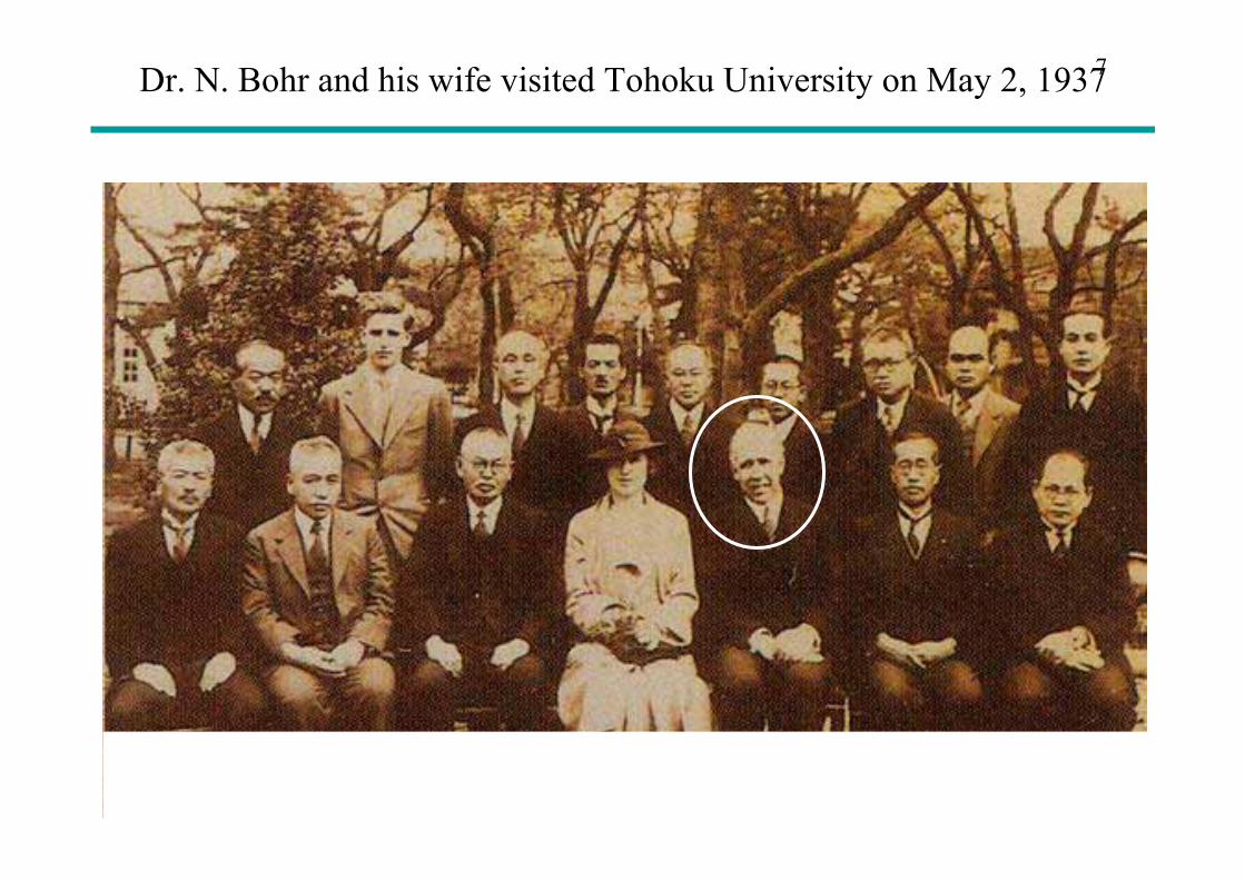
Dr. N. Bohr and his wife visited Tohoku University on May 2, 19377

Outline of Tohoku University-Number of Faculties
Professors: 821Associate Professors: 638Senior Assistant Professors: 153Assistant Professors: 994Research Associates: 69Total: 2,675
-Number of Administrativeand Technical Staff: 2,691
-Number of StudentsUndergraduate: 10,913 Graduate 4,155 (Master Course)
2,740 (Doctor Course)Total: 17,849
・Number of Students/Number of Faculties=6.67
8

Organization of Tohoku University10 undergraduate schools and 15 graduate schools• Graduate School/Faculty of Arts and Letters • Graduate School/Faculty of Education • Graduate School/Faculty of Law • Graduate School of Economics and Management/Faculty of Economics• Graduate School/Faculty of Science• Graduate School/School of Medicine • Graduate School/School of Dentistry • Graduate School/Faculty of Pharmaceutical Sciences • Graduate School/School of Engineering• Graduate School of Agricultural Sciences/Faculty of Agriculture • Graduate School of International Cultural Studies • Graduate School of Information Sciences• Graduate School of Life Sciences• Graduate School of Environmental Sciences• Graduate School of Biomedical Engineering5 Institutes• Institute for Materials Research • Institute of Development, Aging and Cancer • Institute of Fluid Science • Research Institute of Electrical Communication• Institute of Multidisciplinary Research for Advanced Materials
9

The School of Engineering in Tohoku Imperial University wasfounded in 1919 with three departments:• Mechanical Engineering, • Electrical Engineering, and • Applied Chemistry.Departments of • Electrical Communications in 1941• Electronic Engineering in 1958• Information Engineering in 1984
History of School of Engineering 10

Department of Mechanical Systems and DesignDepartment of NanomechanicsDepartment of Aerospace EngineeringDepartment of Quantum Science and Energy EngineeringDepartment of Bioengineering and Robotics
Department of Electrical and Communication EngineeringDepartment of Electronic EngineeringDepartment of Applied Physics
Department of MetallurgyDepartment of Materials ScienceDepartment of Materials Processing
Department of Architecture and Building ScienceDepartment of Civil and Environmental Engineering
Department of Management Science and Technology
Department of Information and Intelligent Systems
Department of Mechanical and Aerospace Engineering
Department of Applied Chemistry, Chemical Engineering and Biomolecular Engineering
Department of Applied ChemistryDepartment of Chemical EngineeringDepartment of Biomolecular Engineering
Department of Civil Engineering and Architecture
Department of Materials Science and Engineering
Graduate School of Engineering (17 Departments)
School of Engineering (5 Departments)
Organization of School/Graduate School of Engineering 11

ECEI GroupECEI Group: Electrical Engineering
Communication EngineeringElectronic EngineeringInformation Engineering
is composed of 1. Graduate School of Engineering
Department of Electrical and Communication EngineeringDepartment of Electronic Engineering
2. Graduate School of Information SciencesDepartment of Computer and Mathematical SciencesDepartment of System Information ScienceDepartment of Applied Information Sciences
3. Graduate School of Biomedical Engineering4. Research Institute of Electrical Communication5. New Industry Creation Hatchery Center (NICHe)6. Cyberscience Center
12

ECEI Group
・Number of FacultiesProfessors: 70Associate Professors: 49Senior Assistant Professors: 1Assistant Professors: 59Research Associate: 1 Total 180
One of the largest electronic and computer engineering complexes in the world.
13

• Yagi-Uda antennaby Prof. H. Yagi and Prof. S. Uda
• Split-anode magnetron tubeby Prof. K. Okabe
• Magnetic recording using AC biasing methodby Prof. K. Nagai
• Pioneer research in electronics by Prof. Y. Watanabe
• Semiconductor science and optoelectronicsby Prof. J. Nishizawa
• High density magnetic recordingby Prof. S. Iwasaki
Outstanding researches in ECEI Group 14

Koichi Tanaka – Prize Award Photo
Photo: Hans Mehlin, Nobel e-Museum
1959 ・Born in Toyama, Japan
1983 ・Graduated from Department of Electrical
Engineering, School of Engineering,
Tohoku University
・Researcher in Shimadzu Corporation
2002 ・The Nobel Prize in Chemistry 2002
“The development of methods for
identification and structure analyses
of biological macromolecules”
・Honorary Doctor of Tohoku University
Mr. Koichi TANAKA, Nobel Laureate
15
15

• The first report describing methods to obtain a sharp beam by using parasitic elements was published by Uda of Tohoku University, Japan in 1925 [1]
• Details of the geometry of the Yagi-Udaantenna were reported by Yagi and Udain 1926 [2].
[1] S. Uda, “On the wireless beam of short electric waves,” J. IEEJ, No. 450, p. 1128, Dec. 1925 (in Japanese).
[2] H. Yagi and S. Uda, “Projector of the Sharpest beam of electric waves,” Proc. Imperial Academy Japan, Vol. 2, No. 2, pp. 49-52, 1926.
Yagi-Uda Antenna
Hidetsugu YAGI(1886-1976)
Shintaro UDA(1896-1976)
16

Geometry of Yagi-Uda Antenna
Reflector elementsExciting element
Director elements
Reflector elements had already been used for directional antennas.Wave directing effects of director elements had not been reported.
17

Uda performed numerous experiments on antennas having many parasitic elements with varying their length and published eleven papers entitled “On the wireless beam of short electric waves” in Journal of IEE Japan in 1926-29.
1. S. Uda, “On the wireless beam of short electric waves (I),” J. IEEJ, No. 452, pp. 273-282, March 1926 (in Japanese).2. S. Uda, "On the wireless beam of short electric waves (II)," J. IEEJ, No. 453, pp. 335-351, April 1926 (in Japanese).3. S. Uda, "On the wireless beam of short electric waves (III)," J. IEEJ, No. 456, pp. 712-724, July 1926 (in Japanese).4. S. Uda, "On the wireless beam of short electric waves (IV)," J. IEEJ, No. 462, pp. 26-51, Jan. 1927 (in Japanese).5. S. Uda, “On the wireless beam of short electric waves (V) -High angle radiation of short wave beam -," J. IEEJ, No.
462, pp. 52-62, Jan. 1927 (in Japanese).6. S. Uda, "On the wireless beam of short electric waves (VI) -Direction control of the beam-," J. IEEJ, No. 465, pp.
396-403, April 1927 (in Japanese).7. S. Uda, "On the wireless beam of short electric waves (VII) -A new electric wave projector-," J. IEEJ, No. 467, pp.
623-634, June 1927 (in Japanese).8. S. Uda, "On the wireless beam of short electric waves (VIII) -Horizontally polarized wave projector-," J. IEEJ, No.
471, pp. 1092-1100, Oct. 1927 (in Japanese).9. S. Uda, "On the wireless beam of short electric waves (IX) -The effects of wave reflector and director on sending
antenna-," J. IEEJ, No. 467, pp. 1201-1219, Nov. 1927 (in Japanese).10. S. Uda, “On the wireless beam of short electric waves (X) -High angle radiation of horizontally polarized waves-,"
J. IEEJ, No. 477, pp. 395-405, April 1928 (in Japanese).11. S. Uda, “On the wireless beam of short electric waves (XI) -Propagation of a few meter waves-," J. IEEJ, No. 492,
pp. 755-770, July 1929 (in Japanese).
Reports on Yagi-Uda Antenna 18

Nd=6
Nd:Number of director elements
Nd=11
Nd=14
S. Uda, “On the wireless beam of short electric waves (VII) -A new electric wave projector-,” J. IEEJ, No. 467, pp. 623-634, June 1927 (in Japanese).
Example of radiation pattern of multi-element Yagi-Uda antenna19

S. Uda, "On the wireless beam of short electric waves (VII) -A new electric wave projector-," J. IEEJ, No. 467, pp. 623-634, June 1927.
Example of radiation pattern of multi-element Yagi-Uda antenna20

• In 1927, Prof. Yagi visited the United States and lectured at several meetings on the experimental results of Yagi-Uda antenna and UHF generating split-anode magnetron tube invented by Okabe of Tohoku University.
• Yagi also published a paper in the Proceedings of IRE in 1928. H. Yagi, “Beam Transmission of Ultra Short Waves,” Proc. IRE, Vol. 16, No. 6, pp. 715-741, June 1928.(Reprint appeared in Proc. IEEE, vol. 72, no. 5, pp. 634-645, May 1985).
• IRE paper stimulated worldwide interests in UHF technology.
• Yagi-Uda antennas were recognized as a useful antenna for VHF and UHF because of the simple but high gain property and were used for radar systems in Europe and America.
• However, little attention was paid to the Yagi-Uda antenna in Japan for radars.
IRE Paper by Prof. Yagi 21

Invention of split-anode magnetron tube
• Albert W. Hull had first invented magnetron in 1921, but the generated power was low.
• Okabe in Tohoku University invented the split-anode magnetron tube, which can generate high power EM wave in VHF and UHF bands.
Kinjiro OKABE(1896-1984)
Magnetic field
Cathode
Anode
22

Electrical Engineering Milestone
• IEEE sent the Electrical Engineering Milestone entitled “Directive Short-Wave Antenna” to Tohoku University, Japan for the outstanding achievement by Yagi and Uda in 1995.
• This is the first Milestone sent to the Asian region.
23

After the invention of Yagi-Udaantenna, Uda started research and development of transmitter and receiver in VHF frequency range.
S. Uda, B. Obara, I. Arisaka, and T. Seki, “Communication tests on ultra short waves between small islands and main land,” J. IEEJ, No. 532, pp. 868-872, Nov. 1932 (in Japanese).
Development of VHF transmitter and receiver 24

Sado Island
Niigata CityJapan Sea
About 50 km
Communication experiments at 65 MHz and 53MHz
• Uda succeeded in communication experiments at 65 MHz and 53 MHz for a distance of about 50 km in 1931.
• These transmitters and receivers using Yagi-Uda antennas were put into police radiotelephone systems between main-land Japan and Sado island in 1933.
25

Sakata City
About 40 km
Tobishima Island
Communication experiments at 38 MHz
• Uda also succeeded in communication experiments at 38 MHz for a distance of about 30 km in 1932.
• These transmitters and receivers using the Yagi-Uda antennas were put into public services of radio wave telecommunication systems between Sakata City and Tobishima Island in 1933.
Japan Sea
26

Uda also performed the development of transmitter and receiver in the UHF frequency range.
S. Uda, “Radiotelegraphy and radiotelephony on half-meter waves,” Proc. IRE, vol. 18, no. 6, pp. 1047-1063, June 1930.
Development of UHF transmitter and receiver 27

Uda succeeded in a communication experiment at a distance of about 30km operating at 600 MHz in 1929, which was the world’s longest record in UHF radio communication.
Communication experiment at 600 MHz
Sendai City
Sendai Bay
Otakamori
MatsushimaBay
28

Replicas of transmitters and receivers using Yagi-Uda antennas
600 MHz tranceiver 600 MHz receiver.
29

MJ =m0
NJ =0
11, HEµε ,
Electric wall
mS
S
22 , HEµε ,
mS
SNJ =m0
MJ 20
01Z
−=
⎪⎭
⎪⎬⎫
−==
21
2201
EHHE Z
Magnetic wall Electric wall
Magnetic wall
Duality of electromagentic field
Electric current density
Magnetic current density
Magnetic current density
Electric current density
][1200
00 Ω≈= π
εµ
Z
Structure #1Structure #2
30

x
y
z
11, HE
NN ′
x
y
z
22 , HE
NN ′−
S
S
Electric wall S
S
(a)Symetric electric current sources
(b) Antisymmetric magnetic currentsources
Babinet’s principle
Electric wall
0,, 212201
><=±= zZ EHHE m
31

Zd ~E2H2
V2I2
adb
c
20( / 2)
sd
ZZ
Z=
][1200
00 Ω≈= π
εµ
Z
Booker ’s relation
Zs ~V1, I1
E1H1
a b
Slot antennaPlanar dipole antenna
Zs:Input impedance of slotantenna
Zd:Input impedance of planar dipole antenna
32
Y. Mushiake, “The input impedances of slit antennas,” J. IEE Japan, vol. 69, no. 3, pp.87-88, March 1949 (in Japanese).S. Uda and Y. Mushiake, “The input impedances of slit antennas,” Tech. Rep. Tohoku Univ., vol. 14, no. 1, pp. 46-59, Sep. 1949.H. G. Booker, “Slot aerials and their relation to complementary wire aerials,” Proc. IEE pt. IIIA, vol. 90, no. 4, pp. 620-629, April 1946.
Y. Mushiake, “The input impedances of slit antenna,” Joint Convention Record of Tohoku Sections of IEE and IECE of Japan, pp.25-26, June 1948 (in Japanese).

Yasuto MUSHIAKE(1921-)• Mushiake in Tohoku University originated self-
complementary structures and found that the input impedance of self-complementary antennas is constant independently of the frequency.
Mushiake’s relation
Ω≈≈= 1886021
0 πZZin
Self-complementary antennas
33
Mushiake's Relationship
V. H. Rumsey, “Frequency Independent Antennas,” 1957 IRE National Conv. Record, pt. I, pp.114-118, March 1957. V. H. Rumsey, “Frequency Independent Antennas,” Academic Press, New York, 1966.

~
• Self-complementary antennas are very interesting since there is an infinite variety of self-complementary structures.
• Rumsey [1] and DuHamel [2] found the importance of the principle of self-complementarity.
• DuHamel [1] developed a wideband planar antenna based on the principle of the self-complementarity using log-periodically spaced notches and monopoles.
Rn+1Rn
1 : Const.n
n
RR
τ +=
Self-complementary antenna having monopoles and notches.
Self-complementarity using log-periodically spaced notches and monopoles proposed by DuHamel
Self-complementary antennas 34
[1] V. H. Rumsey, “Frequency Independent Antennas,”1957 IRE National Conv. Record, pt. I, pp.114-118, March 1957.[2] R. H. DuHamel and D. E. Isbell, “Broadband logarithmically periodic antenna structures," 1957 IRE National Conv.
Record, pt. I, pp.119-128, March 1957.

Planar self-complementary antenna radiates bi-directionally and a directional antenna wasdesired.
Modified self-complementary antennas
V. H. Rumsey, “Frequency Independent Antennas,” Academic Press, New York, 1966.
35

ψ
ψ
DuHamel tried to deform the structure by bending the planar antenna and obtained a modified self-complementary antenna called a “log-periodic antenna” having directional radiation pattern.
Modified self-complementary antennas
V. H. Rumsey, “Frequency Independent Antennas,”Academic Press, New York, 1966.
R. H. DuHamel and F. R. Ore, “Logarithmically periodic antenna design,” 1958 IRE Int. Conv. Record, pt. I, pp.139-151, March 1958.

Main beam
Main beam
Planar structure
Wire structure
Modified self-complementary antennas 37
R. H. DuHamel and F. R. Ore, “Logarithmically periodic antenna design,” 1958 IRE Int. Conv. Record, pt. I, pp.139-151, March 1958.

Feed point
Coaxial cable
Feed
Log-periodic dipole array antenna
• Log-periodic antenna was further deformed to log-periodic dipole array (LPDA) antenna.
• LPDA antenna has been widely used for extremely wide frequency operation in communications and measurements, especially in EMC measurements.
Main beam
38
D. E. Isbell, “Log periodic dipole arrays,” IRE Trans. Antennas Propagat., vol. 8, no. 3, pp. 260-267, May 1960.

Y. Mushiake, “Constant impedance antennas,” J. IECE, vol. 48, no.4, pp. 580-584, April 1965.
Y. Mushiake, “Self-Complementary Antennas,” IEEE Antennas Propagat. Magazine, vol. 34, no. 6, pp. 23-39, Dec. 1992.
Y. Mushiake, “Self-Complementary Antennas –Principle of Self-complementarity for Constant Impedance,” Springer-Verlag London, 1996.
Y. Mushiake, “Log-periodic structure provides no broad-band property for antennas,” J. IEICE, vol. 82, no. 5, pp. 510-511, May 1999 (in Japanese).
Other papers ralated to self-complementary antennas39

x,y
z
Small loop antenna
• Prior to the 1950’s, loop antennas were used in low frequency range as infinitesimal magnetic dipole.
• Maximum radiation occurs in the direction perpendicular to the axis of loop for the case of electrically small loop antenna.
λπ <<b2 λ :wavelength
40

• The characteristics of a loop antenna changes drastically in the high frequency range and more rigorous treatment was desired.
• Adachi and Mushiake [1] performed analyses of loaded and short-circuited loop antenna as a boundary problem based on the Hallén type integral equation.
• They also derived a compact solution in the first order approximation which is satisfactory for practical purposes [2].
ZL
~
[1] S. Adachi and Y. Mushiake, “Theoretical formulation for circular loop antennas,” Sci. Rep. Research Institute of Electrical Communication, Tohoku Univ., B, vol. 9, no. 1. pp.9-18, May 1957.
[2] S. Adachi and Y. Mushiake, “Studies of large circular loop antennas,”Sci. Rep. Research Institute of Electrical Communication, Tohoku Univ., B, vol. 9, no. 2. pp. 79-103, Sep. 1957.
Saburo ADACHI(1930-)
Large circular loop antenna.
Large loop antenna 41

z
x
y
z
One wavelength loop antenna 42
• Adachi found that a large loop antenna having a conducting wire of one wavelength has maximum radiation in the axial direction.

Loop array antennas
• Because of the high directivity, one wavelength loop antennas are used as elements in arrays such as the Yagi-Uda loop array antenna [1], [2] and the log-periodic loop array antenna [3].
S. Adachi and Y. Mushiake, “Directive loop antennas,” Sci. Rep. Research Institute of Electrical Communication, Tohoku Univ., B, vol. 9, no. 2. pp.
105-112, Sep. 1957.S. Adachi, Y. Mushiake, T. Kasahara, and G. Saito, “Characteristics of loop-
directive antennas and broadening of their frequency bandwidths,” J. IEEJapan, vol.48, no. 4, pp.720-724, April 1965 (in Japanese).B. Rojarayanount and T. Sekiguchi, “A study on log-periodic loop antennas,”
Trans. IECE B, Vol. J60-B, No. 8, pp. 583-589, Aug. 1977 (in Japanese).
43

One wavelengthloop antenna
~Half wavelength
Twin loop antennas
• Twin loop antenna is a type of antennas using one wavelength loop antennas, which have only one driving point but has high gain and wide bandwidth.
44

0.25λ
~
~
Twin loop antennas
• Four element (4L) twin loop antenna and six element (6L) twin loop antenna were also developed in Japan.
• 2L, 4L and 6L twin loop antennas located in front of conducting plane with a spacing of a quarter wavelength have been widely used for UHF TV broadcasting antennas in Japan.
4L twin loop antenna
4L twin loop antenna with reflector.
45
K. Endo, Y. Endo, and H. Okamura, “Stacked loopantenna for UHF television broadcasting,” J. Inst.Television Engineers (ITE) Japan, vol. 18, no. 5, pp.281-287, May 1964 (in Japanese).

Mr. Koichi TANAKA
Prof. Adachi was the supervisor of Mr. Koichi TANAKA (received the Nobel Prize in Chemistry 2002)
46

Current researches in Electromagnetic Wave Engineering Laboratory
Fundamental Studies
EM wave Theory• Theoretical investigation of
scattering and diffraction of EM wave.
• Numerical methods to analyze scattering and diffraction of EM wave (MoM and FDTD).
• Development of highly accurate EM simulators for antennas and EM wave.
Measurement systems of antenna characteristics and EM Fields.
• Measurement of radiation characteristics of antennas.
• Visualization of EM field.
Applications
Antenna EngineeringDevelopment of antennas for • Portable telephone.• Magnetic Resonance Imaging
(MRI)• Production and heating of RF
plasma• Long range RFID systemAdaptive array antennasMIMO
Electromagnetic Compatibility (EMC)• Estimation of source location of
undesired EM wave• Suppression of undesired EM wave
emission
47
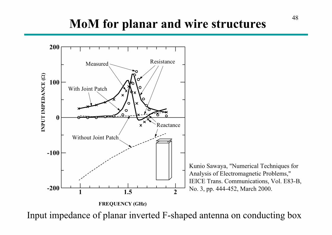
MoM for planar and wire structures
Input impedance of planar inverted F-shaped antenna on conducting boxFREQUENCY (GHz)
INPU
T IM
PED
AN
CE
(Ω)
ResistanceMeasured
With Joint Patch
Without Joint Patch
Reactance
1 1.5 2-200
-100
0
100
200
48
Kunio Sawaya, "Numerical Techniques for Analysis of Electromagnetic Problems," IEICE Trans. Communications, Vol. E83-B, No. 3, pp. 444-452, March 2000.

Folded array antenna used for plasma production
Conductor plateGlass substrateFolded antenna
yx
z
Coaxial cable
x
z
y
z
xy
Antenna No. #1 ~ #25
Glass substrate
[mm]
49
H. Sato, K. Tamashiro, K. Sasaki, T. Takagi, M. Ueda, Y. Watabe, and K. Sawaya, “Design of Folded Monopole Array Antenna Used for Large Area Plasma Production,” 2004 IEEE AP-S International Symposium, Monterey, CA, pp. 1026-1029, June 2004.

Fast measurement system of radiation characteristics of antennas
RF combiner Wideband RF Receiver
ProbeController
Turntable
Computer
Modulation Circuit Box
Receiving Antenna
Device Under Test
Received IF Signal
• 16 modulation probe elements.• 0 to 168.75 degrees in elevation angle. • Cross dipole antenna is used as probe• Horizontal and vertical dipoles are
electrically switched.• Local frequency of 20 MHz to 40
MHz for each probe.• Wideband spectrum analyzer Modulation
probeModulation Circuit
AUT
Turn table
50
Q. Chen, K. Sawaya, T. Habu, and R. Hasumi, “Simultaneous Electromagnetic Measurement Using a Parallel Modulated Probe Array,” IEEE Trans. Electromagnetic Compatibility, Vol. 49, No. 2, pp.263-269, May 2007.

Spectrum of Received Signal
Frequency[GHz]
Rec
evie
d P
ower
[dB
m]
1.05 1.055 1.06 1.065 1.07 1.075-80
-60
-40
-20
0
Spectrum of received IF signal observed by real-time spectrum analyzer. 18 peaks of the spectrum correspond to the RF signal level excited on the 18 modulation probes.
fRF=1GHz
#1#16
51

Manufactured Measurement System
• Cross dipole element• Isolation is more than 30
dB. • Modulation circuit box.
52

Summary of Measurement System
> 30 dBPolarization isolation
< 0.3 dBGain measurement repeatability
16 sec.Total measurement time
2 MHzFrequency bandwidth
800 - 1200 MHzFrequency range
1.03 mRadius of semicircular arch
PerformanceItem
53

Measured 3-D Radiation Pattern
Half wavelength dipole
54

Measurement of Radiation EfficiencyMeasurement of Radiation Efficiency
6.9 D
Salt solution(10 * 10 * 5)
Ground plane (30 * 30)
1.7
27 D
Salt solution(10 * 10 * 5)
Ground plane (30 * 30)Inverted FInverted F--shaped antennashaped antennaMonopole antennaMonopole antenna
• Radiation efficiency is defined by a ratio of radiated power to incident power to the antenna.
• AUT is located in the vicinity of a rectangular container filled with a salt solution.
• Absorbed power in salt solution is a part of the antenna loss.
55

D [cm]
Rad
iatio
n Ef
ficie
ncy
[%]
FDTD Analysis
Measurement
f=1 GHz1% salt solution (εr=77.8, σ=0.39 S/m)
D
0 1 2 3 4 5 6
10
20
30
40
50
60
70
80
90
100
Measured Radiation Efficiency
Monopole antenna
56

D [cm]
Rad
iatio
n Ef
ficie
ncy
[%]
FDTD Analysis
Measurement
f=1 GHz1% salt solution (εr=77.8, σ=0.39 S/m)
D
0 1 2 3 4 5 6
10
20
30
40
50
60
70
80
90
100
Measured Radiation Pattern
Inverted F-shaped antenna
57

RFID tags are required to be compact, low price and long life without any maintenance.
Distance r between the reader and the tag is limited because the received power at the tag from the reader is proportional to the (λ/r)2, and the responding signal power at the reader from the tag is proportional to the (λ/r)4.
Background 58
RFID tag
Base station (reader)
r(λ/r)4
(λ/r)2
0.9 GHz band 10m2.45 GHz band 4m

Passive RFID tag for a range longer than 20 m is proposed for tag systems at 900 MHz band 2.45 GHz band.
A high gain antenna and a rectifying circuit having high multiplying ratio are proposed to obtain long range passive RFID tag system.
Goal 59
RFID tag
Base station (reader)
r
m20>r
• High gain antenna• Rectifying circuit having
high multiplying ratio
H. Kitayoshi and K. Sawaya, “Long Range Passive RFID-Tag for Temperature Monitor System,” Proc. International Symposium on Antennas and Propagation (ISAP2005), Seoul, Korea, pp. 1257-1260, Aug. 2005.
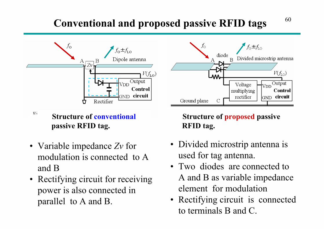
• Variable impedance Zv for modulation is connected to A and B
• Rectifying circuit for receiving power is also connected in parallel to A and B.
• Divided microstrip antenna is used for tag antenna.
• Two diodes are connected to A and B as variable impedance element for modulation
• Rectifying circuit is connected to terminals B and C.
Structure of proposed passive RFID tag.
Structure of conventionalpassive RFID tag.
Conventional and proposed passive RFID tags 60

Received signal level
Fig. 4
PIN diode: Rs=1 Ω, C0=2 pF
61

-10dBm2.45 GHz
50 Ω λ/4 short stub0.15 pF
15 pF15 pF
1 pF
RL=33kΩ
100 nH
10 pF
DC output
D1D2 D3
D1,D2,D3HSMS-286
Tank circuit
Parallel resonance
62Rectifying circuit
Modified 3 stage Cockcroft-Walton circuit

Rectifying circuit 63
Input power=-10 dBmLoad resistance RL=33 kΩ. .

Lomg range RFID Summary• Passive RFID tags for a long reading range have been proposed.• Divided microstrip antenna is used for tag antenna.• Rectifying circuit boosting DC voltage composed of a tank circuit of
a λ/4 short stub and modified Cockcroft-Walton circuit has been proposed.
Size of tags: 90×60×4 mm for 900 MHz band60×25×4 mm for 2.45 GHz band
• Estimation system of location of RFID-tag has been also resented.
64
30 mRCR STD-1(Japan) 0.3 W, 20 dBi 11 mFCC 15.247(U.S.A.) 1 W, 6 dBi
2.45 GHz
30 mFCC 15.247 (U.S.A.)ARIB STD-T89 (Japan)1 W, 6 dBi900MHz
Reading rangeStandard specificationTx power &
antenna gainFrequencyband

Patch antenna elements of adaptive array antenna
Receiver using adaptive array antennaAccess Type: W-CDMA DPCHCarrier Frequency: 2.4GHzBandwidth: 5MHzSampling Clock 3.84MHz×4Number of Array Element: 4Calibration: Blind automatic calibration
Adaptive array antenna 65

Experimental setup for evaluation of adaptive array antenna
Desied signal
Interference
Adaptive array antenna
66

4 monopole Adaptive Array Antenna
Single monopole
SIR [dB]
BER
-25 -20 -15 -10 -5 010-4
10-3
10-2
10-1
100
4 monopole Adaptive Array Antenna
Single monopole
SIR [dB]B
ER-25 -20 -15 -10 -5 010-4
10-3
10-2
10-1
100
13dB
Unechoic chamber
10dB
Indoor
Measured BER 67

Receivingports
Prototype transceiver for wireless LAN Transmission system Single carrier, Frequency domain equalizer
QPSKBaud rate 20MbaudFrequency 2.45 GHzTransmission rate 17.78 MbpsError correction Encoding ratio:1/2, Constraint length:7, ViterbiFilter 50% Root Nyquist Filter
Adaptive array antenna combined with frequency domain equalizer
Transmittingport
68
x#1
y
#Nt
0
DD
EyEzEx
#2
z
3m7m
1.5m
FDTD FDTD methodmethod
TransmitterTransmitter ReceiverReceiver
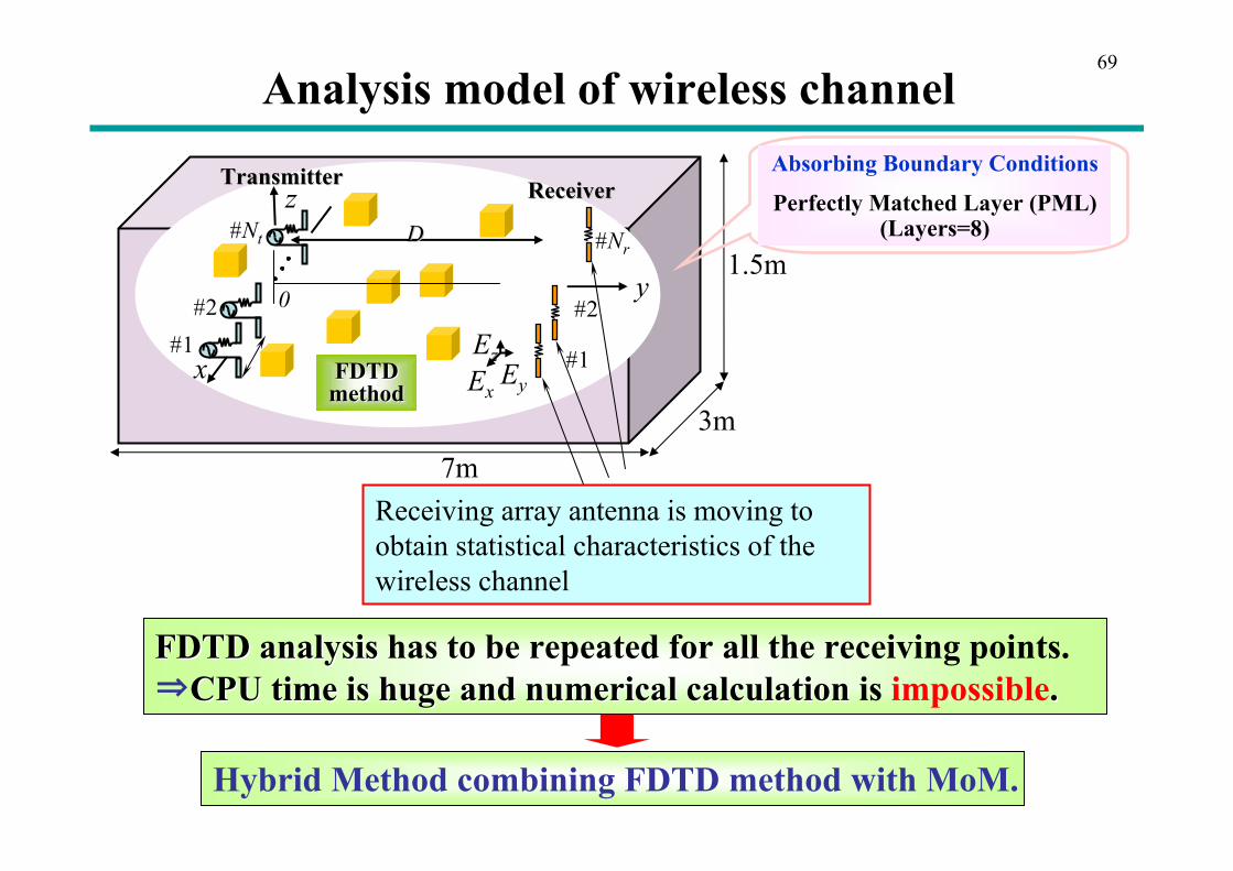
Analysis model of wireless channelAbsorbing Boundary Conditions
Perfectly Matched Layer (PML)(Layers=8)
FDTD analysis FDTD analysis has to be repeated for all the receiving points. ⇒CPU time is huge and numerical calculation CPU time is huge and numerical calculation is impossible..
69
#1
#2
#Nr
Receiving array antenna is moving to obtain statistical characteristics of the wireless channel
Hybrid Method combining FDTD method with MoM.

Hybrid method of FDTD method and MoM
Ez1Ez2
2a
∆z
z( ) ( )
( )zkazzk
zwzf mm
∆−∆
=
=
0
0
sin2sinπ
)(sincos1
)()(
2100
0zz
mm
EEzkkzk
dzV
+∆∆−
=
⋅= ∫ rErw
Moving Area MoM
Absorbing Boundary Conditions
Perfectly Matched Layer (PML)(Layers=8)
Sinusoidal function is used as basis function and weighting function
FDTD is used to analyze transmitting antennas and propagation channel
MoM is used to analyze received voltage
Electric field at every Yee cell inside moving area is calculated by using FDTD
70
5λ
5λ
#1#2#Nr
λ/2
d
Required CPU time can be significantly reduced.
x#1
y
#Nt
0
D
EyEzEx
#2
z
3m7m
1.5m
FDTD method
Transmitter Receiver

Parameters for numerical simulation
8192Time Step (FDTD)
Conducting Cubes withScatterers
Cell Size (FDTD)Number of Yee cells (FDTD)
1.5GHzCarrier FrequencyBPSKModulation
Vertical half wavelength dipole Array Antenna
FixedTransmitting AntennaMoving (in several wavelengths)Receiving AntennaUniform Power Allocation
Fixed regardless of KTransmitted power
222 λλλ ××
150701301 ××cm1cm1cm1 ××
71
X. P. Yang, K. Yamaguchi, Q. Chen, and K. Sawaya, “Numerical Simulation for MIMO Wireless Channel by Using Hybrid Method of FDTD and MoM,” Proc. International Symposium on Antennas and Propagation (ISAP ‘04), Sendai, Japan, vol. 1, pp. 313-316, Aug. 2004.

… …
Tra
nsm
itter
Rec
eive
r
Rich multipath environment, but small received signal
Total radiation power Pr
Ns is large.
Number of scatterers Ns is small.
… …
Tra
nsm
itter
Rec
eive
r
Nt
Poor multipath environment, but large received signal
Effect of number of scatterers Ns72
Nt Nr
Nr

Comparison of fixed and moving receiving antennas
• Hybrid method yields average capacity and BER.• CPU time of hybrid method for statistic evaluation is much
shorter than that of FDTD (1:12,000).
73
Ns: number of scatterers
b 0
Receiving antennas is fixedFDTD method
0 10 20 30
10
20
30
40
Cap
acity
[bps
/Hz]
Ns=0Ns=100
Ns=300
Ns=500
Received Eb/N0 [dB]0 10 20 30
10
20
30
40
Cap
acity
[bps
/Hz]
Ns=0Ns=100
Ns=300
Ns=500
Received Eb/N0 [dB]b 0
Receiving antennas is movingHybrid method
0 10 20 30
10
20
30
40
Cap
acity
[bps
/Hz]
Ns=0Ns=100
Ns=300
Ns=500
Received E /N [dB]0 10 20 30
10
20
30
40
Cap
acity
[bps
/Hz]
Ns=0Ns=100
Ns=300
Ns=500
Received E /N [dB]
Channel capacity versus received Eb/N0Nt=Nr=4

Received Eb/N0 [dB]
Cap
acity
[bps
/Hz]
Ns=0
Ns=300Ns=500
Ns=100
0 10 20 30
10
20
30
40
74
Capacity and BER versus received Eb/N0
• Capacity increases and BER decreases as number of scatterers increases.
Ns: number of scatterers
BER
Received Eb/N0 [dB]
Ns=0
Ns=100
Ns=300Ns=500
0 10 20 3010-4
10-3
10-2
10-1
100
Nt=Nr=4
BER
Transmitted Power [dBm]
Ns=0
Ns=100
Ns=300
Ns=500
-60 -50 -40 -3010-4
10-3
10-2
10-1
100
Cap
acity
[bps
/Hz]
Transmitted Power [dBm]
Ns=0
Ns=100Ns=300
Ns=500
-60 -50 -40 -300
10
20
30
40
75
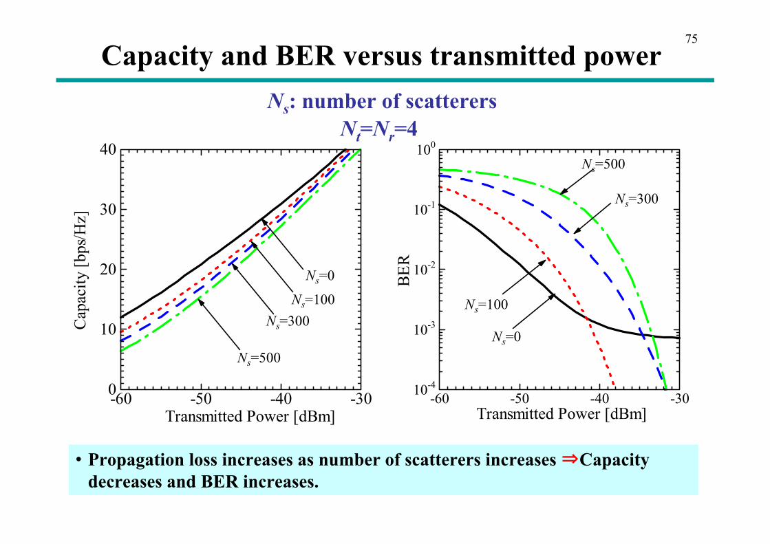
Capacity and BER versus transmitted power
• Propagation loss increases as number of scatterers increases ⇒Capacity decreases and BER increases.
Ns: number of scatterersNt=Nr=4

Simulation of MIMO Summary
A hybrid method combining FDTD method with MoM has been proposed for simulation of the MIMO wireless channel analysis.
Channel capacity and bit error rate have been analyzed using realistic antenna and propagation model.
The numerical results indicate that -both the effect of propagation channel and the antenna
properties should be included in the analysis of MIMO-propagation loss due to scatterers should be incorporated
76

ECEI Group of Tohoku University- One of the largest electronic and computer engineeringcomplexes in the world
- Outstanding researches have been achievedHistorical review of researches on antenna engineering
- Yagi-Uda Antenna- Self-complementary antenna- One wavelength loop antenna
Current researches in Electromagnetic Wave Engineering Laboratory- Method of Moments (MoM)- Finite Difference Time Domain (FDTD)- Fast measurement system of radiation characteristics of antennas
- Long range RFID- Adaptive array antenna- Realistic simulation of MIMO
Conclusion77