Embed Size (px)
Citation preview
Pu et al. Nanoscale Res Lett (2021) 16:101 https://doi.org/10.1186/s11671-021-03554-7
NANO REVIEW
Review of Recent Progress on Vertical GaN-Based PN DiodesTaofei Pu1,2, Usman Younis1, Hsien‑Chin Chiu3, Ke Xu4, Hao‑Chung Kuo5 and Xinke Liu1*
Abstract
As a representative wide bandgap semiconductor material, gallium nitride (GaN) has attracted increasing attention because of its superior material properties (e.g., high electron mobility, high electron saturation velocity, and critical electric field). Vertical GaN devices have been investigated, are regarded as one of the most promising candidates for power electronics application, and are characterized by the capacity for high voltage, high current, and high break‑down voltage. Among those devices, vertical GaN‑based PN junction diode (PND) has been considerably investigated and shows great performance progress on the basis of high epitaxy quality and device structure design. However, its device epitaxy quality requires further improvement. In terms of device electric performance, the electrical field crowding effect at the device edge is an urgent issue, which results in premature breakdown and limits the releasing superiorities of the GaN material, but is currently alleviated by edge termination. This review emphasizes the advances in material epitaxial growth and edge terminal techniques, followed by the exploration of the current GaN develop‑ments and potential advantages over silicon carbon (SiC) for materials and devices, the differences between GaN Schottky barrier diodes (SBDs) and PNDs as regards mechanisms and features, and the advantages of vertical devices over their lateral counterparts. Then, the review provides an outlook and reveals the design trend of vertical GaN PND utilized for a power system, including with an inchoate vertical GaN PND.
Keywords: Gallium nitride, Vertical PN junction diode, Electrical field crowding, Edge termination techniques
© The Author(s) 2021. Open Access This article is licensed under a Creative Commons Attribution 4.0 International License, which permits use, sharing, adaptation, distribution and reproduction in any medium or format, as long as you give appropriate credit to the original author(s) and the source, provide a link to the Creative Commons licence, and indicate if changes were made. The images or other third party material in this article are included in the article’s Creative Commons licence, unless indicated otherwise in a credit line to the material. If material is not included in the article’s Creative Commons licence and your intended use is not permitted by statutory regulation or exceeds the permitted use, you will need to obtain permission directly from the copyright holder. To view a copy of this licence, visit http:// creat iveco mmons. org/ licen ses/ by/4. 0/.
IntroductionGlobal energy consumption is rising much more rapidly than in the past few decades because of the rapid growth in industry and economy. Therefore, advanced energy-saving technologies are required to alleviate the issues of increasing energy consumption.
Silicon-based devices are currently the dominant type among power devices [1]. Among these power devices, the insulated gate bipolar transistor (IGBTs) structures play a significant role and display a growing trend toward the replacement of the power bipolar junction transis-tor (BJT) and metal oxide semiconductor field effect transistor (MOSFET) since the invention of the IGBTs
in 1982 [2]. Presently, IGBTs are essential elements of power electronic fields for conversion and transmission [3]. However, silicon-based power devices have reached their fundamental material limits to date and are utilized widely in electric energy application.
Given its outstanding properties, GaN is one of wide bandgap semiconductor materials (including SiC, GaN, Ga2O3 and diamond) capable of fabricating power devices with a low capacitance and resistance for a speci-fied breakdown voltage with respect to the Si-based devices. Thus, GaN-based devices with low energy con-sumption, high power densities, and high conversion effi-ciency for power electronic systems are expected.
As shown in Table 1, GaN has a much higher Baliga’s figure of merit (BFOM) than SiC (which has been com-mercialized), a feature which is ascribed to its higher electron saturation velocity and higher critical electrical field. However, SiC has better thermal conductivity. In
Open Access
*Correspondence: [email protected] College of Materials Science and Engineering, Shenzhen University–Hanshan Normal University Postdoctoral Workstation, Shenzhen University, Shenzhen 518060, ChinaFull list of author information is available at the end of the article
Page 2 of 14Pu et al. Nanoscale Res Lett (2021) 16:101
addition, GaN possesses a higher carrier mobility µ and a higher thermal conductivity, and achieved both p- and n-type doping compared to Ga2O3. Meanwhile, for the ultimate wide bandgap semiconductor, diamond, consid-erable progress must be achieved to reach the practical stage. To date, GaN-based devices, e.g., three-terminal device (Heterostructure field-effect transistors (HFETs) and MOSFETs) and two-terminal devices (SBDs and PNDs) have become key research topics, and great pro-gress has been achieved in their applications in power rectification and power conversion.
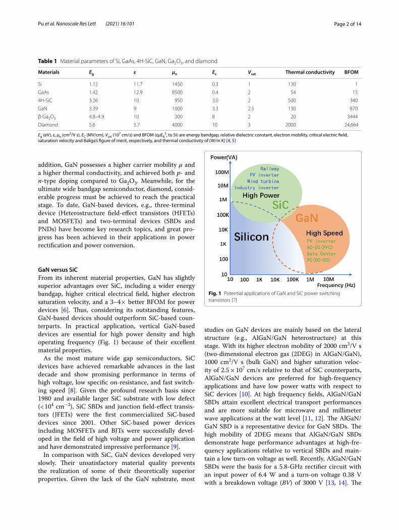
GaN versus SiCFrom its inherent material properties, GaN has slightly superior advantages over SiC, including a wider energy bandgap, higher critical electrical field, higher electron saturation velocity, and a 3–4× better BFOM for power devices [6]. Thus, considering its outstanding features, GaN-based devices should outperform SiC-based coun-terparts. In practical application, vertical GaN-based devices are essential for high power density and high operating frequency (Fig. 1) because of their excellent material properties.
As the most mature wide gap semiconductors, SiC devices have achieved remarkable advances in the last decade and show promising performance in terms of high voltage, low specific on-resistance, and fast switch-ing speed [8]. Given the profound research basis since 1980 and available larger SiC substrate with low defect (< 104 cm−2), SiC SBDs and junction field-effect transis-tors (JFETs) were the first commercialized SiC-based devices since 2001. Other SiC-based power devices including MOSFETs and BJTs were successfully devel-oped in the field of high voltage and power application and have demonstrated impressive performance [9].
In comparison with SiC, GaN devices developed very slowly. Their unsatisfactory material quality prevents the realization of some of their theoretically superior properties. Given the lack of the GaN substrate, most
studies on GaN devices are mainly based on the lateral structure (e.g., AlGaN/GaN heterostructure) at this stage. With its higher electron mobility of 2000 cm2/V s (two-dimensional electron gas (2DEG) in AlGaN/GaN), 1000 cm2/V s (bulk GaN) and higher saturation veloc-ity of 2.5 × 107 cm/s relative to that of SiC counterparts, AlGaN/GaN devices are preferred for high-frequency applications and have low power watts with respect to SiC devices [10]. At high frequency fields, AlGaN/GaN SBDs attain excellent electrical transport performances and are more suitable for microwave and millimeter wave applications at the watt level [11, 12]. The AlGaN/GaN SBD is a representative device for GaN SBDs. The high mobility of 2DEG means that AlGaN/GaN SBDs demonstrate huge performance advantages at high-fre-quency applications relative to vertical SBDs and main-tain a low turn-on voltage as well. Recently, AlGaN/GaN SBDs were the basis for a 5.8-GHz rectifier circuit with an input power of 6.4 W and a turn-on voltage 0.38 V with a breakdown voltage (BV) of 3000 V [13, 14]. The
Table 1 Material parameters of Si, GaAs, 4H‑SiC, GaN, Ga2O3, and diamond
Eg (eV), ε, µn (cm2/V s), EC (MV/cm), Vsat (107 cm/s) and BFOM (εµEb3, to Si) are energy bandgap, relative dielectric constant, electron mobility, critical electric field,
saturation velocity and Baliga’s figure of merit, respectively, and thermal conductivity of (W/m K) [4, 5]
Materials Eg ε µn Ec Vsat Thermal conductivity BFOM
Si 1.12 11.7 1450 0.3 1 130 1
GaAs 1.42 12.9 8500 0.4 2 54 15
4H‑SiC 3.26 10 950 3.0 2 500 340
GaN 3.39 9 1000 3.3 2.5 130 870
β‑Ga2O3 4.8–4.9 10 300 8 2 20 3444
Diamond 5.6 5.7 4000 10 3 2000 24,664
Fig. 1 Potential applications of GaN and SiC power switching transistors [7]
Page 3 of 14Pu et al. Nanoscale Res Lett (2021) 16:101
maximum cutoff frequency is close to 1 THz at 0 V with an anode-to-cathode distance of 70 nm [15].
For GaN-based power devices, the GaN substrate (bulk GaN) is ideal for epitaxy growth, which could uti-lize homo-epitaxy technology to eliminate the mismatch. The low dislocation density of bulk GaN is essential for the epitaxial substrate because the high dislocation den-sity can affect performance characteristics such as BV, reverse leakage current, production volume, and reliabil-ity [16]. The developments of vertical GaN-based devices have been driven by the progress of the GaN substrate in recent years. However, given the relatively immature technology for the vertical triode, the vertical GaN diode has become a hot research topic at this initial stage. Com-pared to AlGaN/GaN SBDs, vertical GaN SBDs have sim-ilar advantages at frequency fields such as high switching speed with low reverse recovery time and low conduction loss; nevertheless, the latter has large current density and less leakage path than the former [17, 18].
Some issues have arisen for the GaN substrate. First, GaN substrates are currently available with dislocation densities of 104–106 cm−2, but these dislocation densities are still much higher than those of Si and SiC substrates [19]. Second, with respect to the 4–6 inch wafer size and reasonable cost (10 euro/cm2) of SiC, the 2–3 inch size and relatively high cost (100 euro/cm2) of the GaN sub-strate inhibit GaN commercialization and productivity on a large scale [20]. Aside from increasing the supply-ing vendors, the heteroepitaxy on foreign substrates (Si, sapphire, or SiC) is an alternative way to reduce the cost of GaN substrate, but the challenge of relatively high mis-match and defects must be addressed.
In addition to the aforementioned issues in bulk mate-rials, the challenge for the GaN diode is to achieve a high quality of the p-type material. With respect to the rela-tively advanced techniques for forming p-type SiC by Al ion implantation, immature p-type ion implantation technology and the low acceptor activation for p-type GaN are vital hindrances, which limit the development of the structure and fabrication of GaN-based devices. Thus, different kinds of edge termination structures are proposed to improve the GaN diode performance and constitute a key part of this review.
Vertical GaN‑Based Devices on the FS‑SubstrateUntil 10 years ago, most GaN diodes, including SBDs and PNDs, were fabricated on foreign substrates form-ing lateral or quasi-vertical device structures because of the unavailability of a bulk GaN substrate. Lateral or quasi-vertical diodes show outstanding electrical char-acteristics, but they still suffer from inherent drawbacks from the device structure [21]. First, the mismatch and defects are inevitable. Then, for GaN devices on foreign
substrates, a buffer is essential between the GaN drift layer and foreign substrate. Thus, the stress relaxation of the buffer layer would cause a wafer bowing, which will lower the thickness of the GaN epitaxy layers [22]. In addition, the large thermal boundary resistance (GaN with substrate) has a serious influence on device perfor-mance for the GaN devices working at high power den-sity [23].
According to the development of epitaxy techniques, free-standing GaN (FS-GaN) substrate with low disloca-tion density adopted for vertical GaN devices has made great progress. The material quality of homoepitaxial GaN on the FS-GaN substrate has an obvious improve-ment and shows the potential for power applications. Vertical GaN devices could mitigate the drawbacks of lat-eral GaN counterparts. First, thicker GaN epitaxial layers can be grown without any buffer, and higher BV (which exceed that of lateral GaN devices) can be obtained and determined by the thickness of the drift layer. Meanwhile, a maximum electric field is located at the inner part of devices and is far from the device surface (eliminating the effect of electron trapping which generally occurs in lat-eral devices). Given the high quality of the FS-GaN sub-strate, vertical GaN devices have been studied since 2011 [24]. Since then, vertical GaN PNDs with high BV and low on-state resistance have been fabricated and achieve remarkable performance.
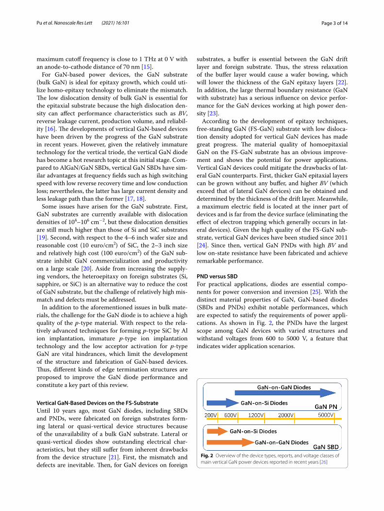
PND versus SBDFor practical applications, diodes are essential compo-nents for power conversion and inversion [25]. With the distinct material properties of GaN, GaN-based diodes (SBDs and PNDs) exhibit notable performances, which are expected to satisfy the requirements of power appli-cations. As shown in Fig. 2, the PNDs have the largest scope among GaN devices with varied structures and withstand voltages from 600 to 5000 V, a feature that indicates wider application scenarios.
Fig. 2 Overview of the device types, reports, and voltage classes of main vertical GaN power devices reported in recent years [26]
Page 4 of 14Pu et al. Nanoscale Res Lett (2021) 16:101
Compared with PNDs, which have no minority car-rier storage issue and lower SBD barrier height, GaN SBDs feature a low forward turn-on voltage (Von) and fast reverse recovery, and these characteristics indicate that the merits of SBD are revealed in low conduction/switching loss, high-frequency operation, but a lower BV value than that of PND; moreover, note that high turn-on voltage can lead a high conduction loss and degrade the efficiency of circuits and systems [27, 28].
At the high-power fields, quasi-vertical or vertical SBDs have excellent advantages over AlGaN/GaN SBDs [29]. Moreover, a low turn-on voltage (< 0.5 V) is achieved by adjusting the barrier height with a low work function metal. However, a low barrier height may easily lead to the high reverse leakage current and lower the BV. Con-sequently, varied edge termination structures are pro-posed to improve performance. Through the assistance of varied edge termination technologies [27, 28, 30, 31], the high current density at KA/cm2 grade with BVs over 1 kV is confirmed. Meanwhile, vertical SBDs also exhibit great capability for high frequency, such as 177–183 GHz and a maximum of 902 GHz cutoff frequency at 0 V, a feature which is expected for power sources in terahertz-wireless communication systems [12, 32].
With respect to n-type GaN, the p-type GaN grown by metalorganic chemical vapor deposition (MOCVD) and molecular beam epitaxy (MBE) was introduced by using Mg as an acceptor [33]. Compared with GaN SBDs, GaN PNDs have many advantages, such as low specific on-resistance (RonA) and adequate device stability and capability of inhibiting surge currents. Despite the high turn-on voltage (> 3 V) and relatively low switching speed, an ultralow leakage current because of the higher barrier height and high BV is obtained. Note that a high BV from 0.6 to 5 kV is the most outstanding performance for GaN-based PNDs. Thus, GaN-based PNDs have great potential as important building blocks of the next-gener-ation power systems for high power applications, which require high efficiency and low energy loss [34]. Similar to vertical GaN SBDs, the edge terminations for GaN PNDs are also fabricated to alleviate electric field crowd-ing around anode, a feature that would be described in detail later in this article.
In power devices, the PN junction can be also treated as a novel junction structure. For utilizing a high BV with low reverse leakage current of PNDs, high switching per-formance and low turn-on voltage of SBDs at the same time, novel device structures including the junction bar-rier Schottky (JBS) and merged PN Schottky (MPS) gen-erate a combination of SBD and PND by the formation of p-type grid regions in the Schottky contact region. JBS or MPS devices possess the characteristics of for-ward conduction of SBDs and reverse blocking of PNDs
and are expected to have better switching performance and higher reverse voltage than conventional PNDs and SBDs, respectively [35].
Besides their high-power application, GaN PNDs are also adopted for optoelectronic devices such as light-emitting diodes (LEDs), photodetectors, and for flame sensing because of the low dark currents of a few pA in GaN-based PN junction photodiodes [36, 37].
Purpose of This ReviewOn the basis of the superior material properties of GaN, GaN-based devices have been investigated widely and utilized in power electronics applications as the one of the hottest semiconductor materials. Among GaN-based devices, the vertical GaN-based PND has been consider-ably explored and shows excellent BFOM. The edge ter-minal techniques are also essential to alleviate the electric field crowding around the anode pad.
In this review, the advances in material epitaxy growth and edge terminal techniques as the main emphases are followed by illustrating the current GaN developments, the differences between GaN SBDs and PNDs in terms of mechanisms and features, and the advantages of verti-cal devices over lateral one. This review provides an out-look and reveals the design trend of vertical GaN PNDs utilized for a power system, including inchoate vertical GaN PNDs. The development of epitaxial growth cor-responding to a different layer in vertical GaN PNDs is introduced in Sect. 2. The edge terminal technologies are explored in Sect. 3. In Sect. 4, the vertical GaN PNDs on Si substrate are demonstrated as an alternative method. Finally, the conclusion and outlook of future develop-ment of vertical GaN PNDs are provided.
Material Epitaxy GrowthGaN Substrate of Vertical PNDsAs a mainstream epitaxial process, vertical device epi-taxial layers are currently mainly grown by MOCVD on conductive GaN substrates fabricated by hydride vapor phase epitaxy (HVPE). In this structure, the quality of the substrate directly affects the following epitaxial structure. Many failure mechanisms in the device originate from substrate epitaxy quality [38]. A high quality of conduc-tive GaN substrate must be obtained to further improve the forward and reverse I–V performances, especially the reverse leakage current and BV capability.
Substrate grown by HVPE has been considered as a most convenient method for mass production because of its relatively low cost and reproducibility. However, in the early stage, the immature growth technology meant that GaN substrate grown by HVPE had high background carrier concentration (> 1019 cm−3) and unsatisfactory crystal quality. Therefore, the HVPE was
Page 5 of 14Pu et al. Nanoscale Res Lett (2021) 16:101
not adopted to grow the device structure [39]. By the rapid development of epitaxy growth technology, high-quality bulk GaN materials by HVPE become gradually possible [40, 41]. Aside from the substrate, the partially epitaxial layer in device can now be grown by HVPE and can result in higher current uniformity and the elimination of the macrostep on the GaN surface by combining HVPE and the MOCVD epitaxial process with carbon-free technology compared devices grown solely by MOCVD [42].
Currently, a commercial GaN substrate with mini-mum dislocation density of less than 104 cm−2 is avail-able. The GaN vertical PNDs on low defect density GaN substrate were processed. However, wafer bowing remains an issue. As a promising solution, the ammon-othermal method can achieve a GaN substrate with better epitaxy quality. With the high-pressure auto-claves and supercritical ammonia, the threading dis-location can be significantly reduced to 104–105 cm−2 [43]. Using the ammonothermal method, a low resist-ance of 0.001 Ω cm2 in the GaN substrate with highly doped n-type (1 × 10¹⁹–1 × 1020 cm−3) was reported as well as the BV of 3 kV [44]. However, the drawback of the ammonothermal method is the low growth rate of approximately 80–90 μm/day, a feature that is adverse for practical production. Improving the growth rate and maintaining high material quality are also profit-able directions for subsequent research.
In addition to the commercial GaN substrate, some substrates were also investigated for distinctive perfor-mances, including the non-Ga-plane (c-plane) substrates. Generally, a Ga-polar (i.e., c-plane) substrate is employed for a GaN vertical device. Then, the following epitaxial layers show a drastic polarization effect. However, in the opposite direction of the Ga-polar counterparts, the homoepitaxial layers along the N-polar direction dem-onstrate unique device properties because of the higher decomposition temperature and polarity-dependent property [45, 46]. With the N-polar single-crystal FS-GaN substrate, an electric field of 2.2 MV/cm without any edge terminations was achieved, as well as a BV of 2.4 kV with N2O surface plasma treatment and field plate (FP) [46, 47]. As another special GaN substrate, the m-plane also attracts wide attention given its nonpolar property for which the Ga:N was 1:1 in the m-plane with respect to only Ga in the c-polar and only N in the N-polar sub-strates. With this nonpolar GaN substrate, the character-istics of PNDs were reported with the critical electrical field of 2.0 MV/cm and high on/off ratio with no FP or edge termination [48].
N‑GaN Epitaxial TechniquesPrior to the existence of high-quality conductive GaN substrates, GaN PNDs were mainly fabricated on foreign substrates including Si, SiC, and sapphire. Therefore, the structure of devices was always limited to lateral ones. A method based on the lateral structure was proposed to improve the epitaxial quality. Given low threading dis-location (TD) on the window region at lateral devices, the GaN epitaxial layer grown laterally across the mask can achieve a much lower TD density. Thus, lateral epi-taxial overgrowth was performed to grow the GaN epi-taxial layer on a sapphire substrate for lateral PNDs. The reverse leakage current was suppressed by three orders of magnitude [49].
With the development of epitaxial technology, high-quality single-crystal GaN substrates with low disloca-tion densities of 3 × 10⁻⁶ cm−2 became available, and GaN PNDs were fabricated on GaN substrates. Com-bined with upper epitaxial layers by MOCVD grown, the devices show a low leakage current and high BV of 600 V to 4 kV corresponding to drift thickness from 6 to 40 μm [16, 50]. With respect to the device on the sapphire substrate, reverse leakage current and BV significantly improved [51].
With the native GaN substrate, no special buffer layer usually occurs in the PND epitaxial structure like that on a foreign substrate. The effect of the buffer layer in the PND on the GaN substrate was investigated as refer-ence. The existence of a buffer layer means that the drift layer has lower defect density. Meanwhile, a higher BV can be obtained with a thinner drift layer but a thicker buffer layer. The reverse leakage current of the device was improved as well. These device parameters exhibit a strong relationship to the thickness of the buffer layer, which has a slight effect on the forward characteristics of the device [52].
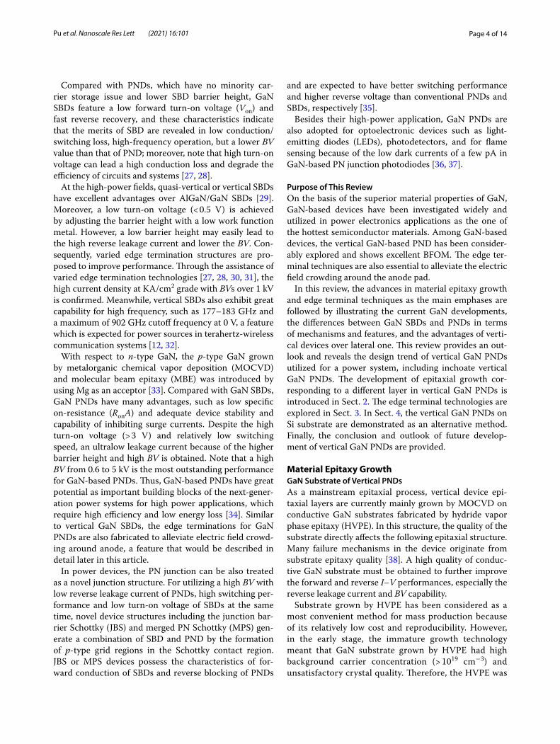
The upper epitaxial layers are deposited by the MOCVD, metal organic vapor phase epitaxy (MOVPE), and MBE, as discussed in this portion. The epitaxial structure of PNDs includes a highly doped n+-GaN layer and a drift layer of n−-GaN between the substrate and p-GaN (Fig. 3). The highly doped n+-GaN layer acts as a transition layer on the conductive GaN substrate in some reports.
In general, the BV determines the application scenarios of devices. For example, the higher BV for a SiC device relative to that with GaN allows the SiC device to be uti-lized in high-power and high-voltage applications like electric vehicles and bullet trains (Fig. 1). Similarly, PN diodes are usually applied in higher voltages with respect to the Schottky diode and HEMTs. In PNDs, the BV is mainly undertaken by the drift layer (lightly doped n−-GaN layer) with the broadening of the depletion region
Page 6 of 14Pu et al. Nanoscale Res Lett (2021) 16:101
(as represented in Eq. 1 with applied voltage V for which V is positive/negative for the forward/reverse bias when the device is under reverse bias. Moreover, the break-down occurs with further increase in the reverse bias.
where S, q, Vbi, ND, and NA are the area of the junction, electronic charge, built-in potential, donor concentra-tion, and acceptor concentration, respectively [53].
According to the depletion width, the devices can be divided into nonpunch-through [WD > WDm (WDm: maximum depletion-layer width)] and punch-through (WD < WDm). Given the issues of epitaxy structure and edge, most GaN vertical devices fall under the punch-through type, i.e., their depletion regions expand beyond the entire n−-GaN layer and reach the n+-GaN substrate prior to breakdown.
Moreover, as described in Eq. (2), the BV can be enhanced by increasing the thickness and decreasing the n-type doping concentration of the drift layer.
where EC, q, t, ND, and εr are the critical electric field, electron charge, n−-GaN layer thickness, net carrier concentration of the n−-GaN layer, and semiconductor permittivity, respectively [54]. Fortunately, experience indicates that a drift layer with thicker thickness and lower doping contributes only to a slight increase for on-state resistance in forward conduction.
Compared with enhancing the BV by increasing the drift layer thickness, decreasing of the n-type doping concentration in the n−-GaN layer is currently difficult, because of the high background concentrations including those of Si, O and so on. For further decrease in the dop-ing concentration in the n−-GaN layer, the unintentional doping concentration is investigated. Many research groups introduced a nominal i-GaN approximate
(1)WD =
√
2εs(Vbi − V )
q
NA + ND
NAND
(2)BV = ECt −qNDt
2
2ε0εr
1015–1016 cm−3 contacting p-GaN to form the p–i–n structure to improve the BV of diodes [55].
Certainly, the precondition of these measures is a high epitaxial quality of the drift layer owing because the TDs can increase the off-state leakage and degrade the BV properties [56].
To further improve the epitaxial quality of the drift layer in GaN vertical PNDs, growth by MBE was inves-tigated on the GaN substrate. A leakage current of less than 3 nA/cm2 and electric field of 3.1 MV/cm were obtained by the very low dislocation density. The nearly ideal breakdown performances indicate that the MBE is an effective method for growing epitaxial layers in GaN vertical PNDs [56]. However, similar to ammonothermal growth, the epitaxial rate is another disadvantage.
P‑GaN EpitaxyP-GaN, an important component in GaN vertical PNDs, was reported in 1989 since the appearance of GaN by HVPE in 1969 [57, 58]. It was first utilized to obtain blue LED. Then, the p-GaN was gradually employed at electric devices field such as normally-off devices and PNDs. In vertical GaN PNDs, the p-GaN constitutes light (around 1019 cm−3) and heavy (≥ 1020 cm−3) doping concentra-tion, which correspond to forming a PN junction layer with the drift layer and facilitating ohmic contacts as the anode electrode.
Generally, the epitaxial growth of a p-GaN is fabri-cated by MOCVD at a temperature of about 1000 °C and adopts the Mg2+ as acceptor. Then, the grown p-GaN layer must be activated at high temperatures of 700–800 °C in N2 ambient or 400 °C in O2 ambient, thereby facilitating a relatively high hole concentration [59–61]. However, the high ionization energy of 150–200 meV of Mg-H bond means a p-GaN activation rate of only 1–3%. A low activation rate is also related to the temperature. The Mg dopants can be re-passivated in high tempera-tures of ≥ 600 °C in NH3 or hydrogen ambient [62]. To improve hole concentration, solely raising the doping concentration is not feasible because a higher doping concentration in the p-GaN could lead to a deterioration of the crystalline quality of the layer and reduce the hole density through a self-compensation effect [63]. At pre-sent, a peak of hole density can usually be achieved at an acceptor concentration of approximately 3 × 1019 cm−3 [64]. Although being some issues for p-GaN, related investigation reports are not much. It may be ascribed to two reasons. One is the limitations of the intrinsic properties of material and epitaxial equipment. Another is that the present p-GaN can also obtain comparative device performance.
However, the optimization of the growth condition and novel epitaxial process are still being investigated. For
Cathoden+-GaN Substrate
n+-GaN
p-GaNAnode
n--GaN
Fig. 3 Schematic structure and fabrication process of GaN vertical PND
Page 7 of 14Pu et al. Nanoscale Res Lett (2021) 16:101
example, in 2017, the non-activated regrown p-GaN by MBE was proposed and has an advantage over MOCVD. With the low hydrogen growth environment, a BV of 1.1 kV and ideality factor of 2.5 were achieved by the fabricated vertical GaN PNDs [65]. Another interesting p-GaN fabrication method is Mg ion implantation with an ultra-high-pressure annealing (UHPA) process. The results reveal that a high activation ratio of 70% and hole mobility of 24.1 cm2V−1 s−1 were achieved with a post-implantation annealing at temperature of 1573–1753 K in N2 pressure of 1 GPa. This result is comparable with that of epitaxy growth by MOCVD [66].
In conclusion, for substrate, the commercial low defect GaN substrate is now available. Meanwhile, epitaxial technology is still developing, a situation which strongly affects on device performances. In comparison with MOCVD, the MBE can achieve excellent epitaxial qual-ity, thereby resulting in great device performance without any edge terminations. However, its slow growth rate and high cost render the MBE unfit for large-scale productiv-ity. The epitaxy growth by MOCVD is still the main pro-ductive method in practice. Thus, improving the quality of epitaxial layers grown by MOCVD is an urgent issue, which would take considerable time. Therefore, advanced device structure design or measures are proposed for great performance at this stage.
Edge Termination TechniquesFor a vertical GaN PNDs, BV is an important parameter. Almost all investigations on vertical GaN PNDs are cen-tered on improving the withstanding voltage at reverse (i.e., BV). However, due to the electric field crowding at the edge of PN junction, the depletion layer edge, or the electrode edge, premature breakdown often occurs. Therefore, to reduce the electric field crowding of the device, advanced device structure designs (i.e., edge ter-mination techniques) are developed. Varied edge ter-mination techniques have now been adopted to relax the electric field crowding at the edge of GaN PNDs for a higher BV. These techniques include mainly the field plate (FP), ion implantation and plasma treatment, and mesa etching in varied angle or steps and guard rings (GRs) [49, 67–69]. These features are discussed in this section.
Metal Field PlatesThe FP has been widely utilized in GaN-based devices for transferring the peak electric field far from the edge of the gate, anode, or junction. This method has an identical feature to relax the intensity of the electric field at the PN edge under reverse bias. Moreover, the low leakage cur-rent and high breakdown voltage under reverse voltage
can be achieved by using FP termination, which has a relatively simple fabricating process as well.
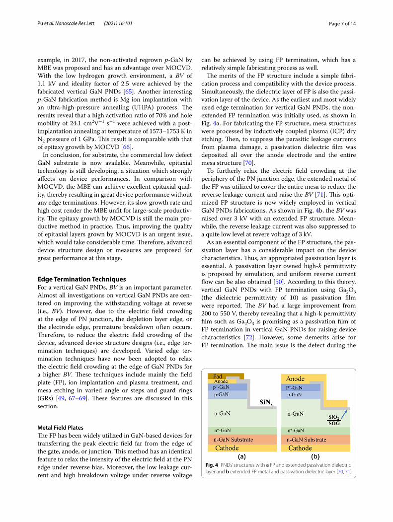
The merits of the FP structure include a simple fabri-cation process and compatibility with the device process. Simultaneously, the dielectric layer of FP is also the passi-vation layer of the device. As the earliest and most widely used edge termination for vertical GaN PNDs, the non-extended FP termination was initially used, as shown in Fig. 4a. For fabricating the FP structure, mesa structures were processed by inductively coupled plasma (ICP) dry etching. Then, to suppress the parasitic leakage currents from plasma damage, a passivation dielectric film was deposited all over the anode electrode and the entire mesa structure [70].
To furtherly relax the electric field crowding at the periphery of the PN junction edge, the extended metal of the FP was utilized to cover the entire mesa to reduce the reverse leakage current and raise the BV [71]. This opti-mized FP structure is now widely employed in vertical GaN PNDs fabrications. As shown in Fig. 4b, the BV was raised over 3 kV with an extended FP structure. Mean-while, the reverse leakage current was also suppressed to a quite low level at revere voltage of 3 kV.
As an essential component of the FP structure, the pas-sivation layer has a considerable impact on the device characteristics. Thus, an appropriated passivation layer is essential. A passivation layer owned high-k permittivity is proposed by simulation, and uniform reverse current flow can be also obtained [50]. According to this theory, vertical GaN PNDs with FP termination using Ga2O3 (the dielectric permittivity of 10) as passivation film were reported. The BV had a large improvement from 200 to 550 V, thereby revealing that a high-k permittivity film such as Ga2O3 is promising as a passivation film of FP termination in vertical GaN PNDs for raising device characteristics [72]. However, some demerits arise for FP termination. The main issue is the defect during the
Fig. 4 PNDs’ structures with a FP and extended passivation dielectric layer and b extended FP metal and passivation dielectric layer [70, 71]
Page 8 of 14Pu et al. Nanoscale Res Lett (2021) 16:101
dielectric layer deposition and interface between the die-lectric and GaN, which result in carrier trapping. These would lead to the instability of device performance dur-ing long-term use. Therefore, the optimized deposition process of the dielectric layer must be investigated.
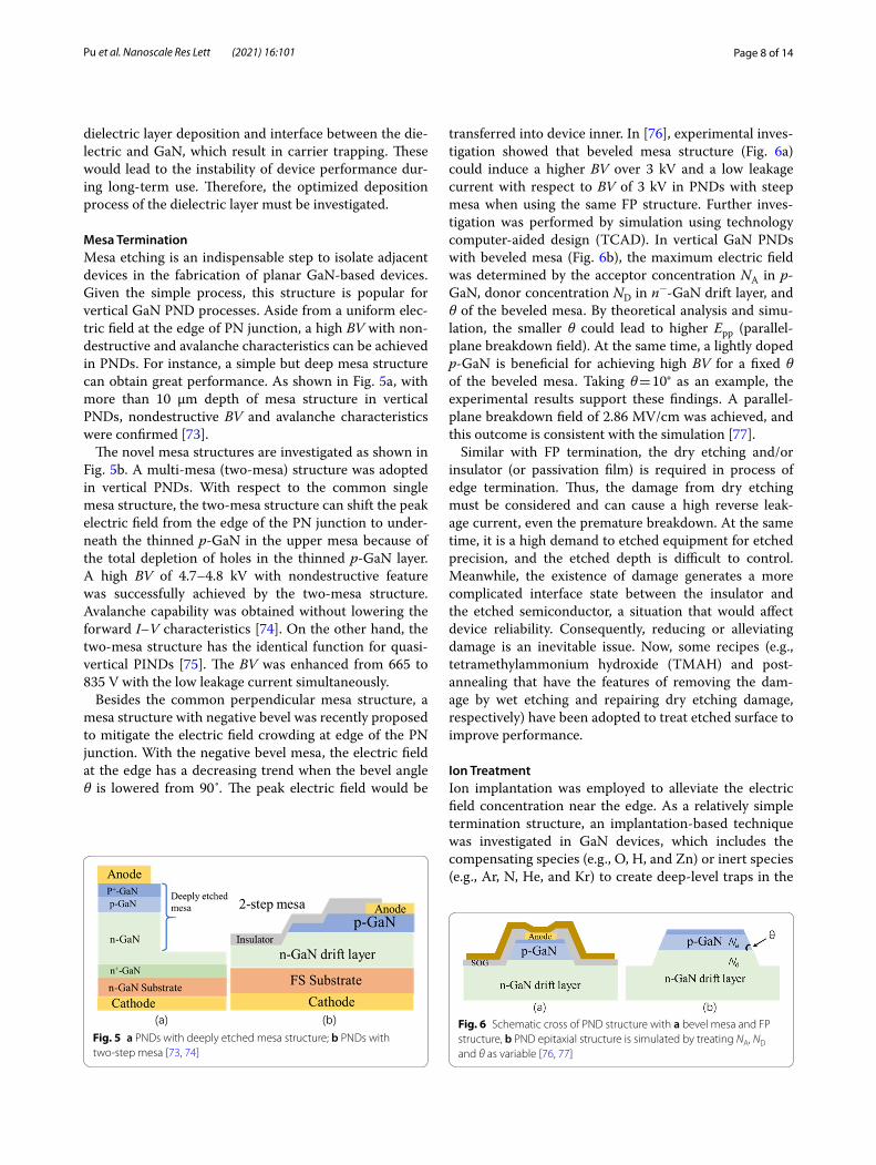
Mesa TerminationMesa etching is an indispensable step to isolate adjacent devices in the fabrication of planar GaN-based devices. Given the simple process, this structure is popular for vertical GaN PND processes. Aside from a uniform elec-tric field at the edge of PN junction, a high BV with non-destructive and avalanche characteristics can be achieved in PNDs. For instance, a simple but deep mesa structure can obtain great performance. As shown in Fig. 5a, with more than 10 µm depth of mesa structure in vertical PNDs, nondestructive BV and avalanche characteristics were confirmed [73].
The novel mesa structures are investigated as shown in Fig. 5b. A multi-mesa (two-mesa) structure was adopted in vertical PNDs. With respect to the common single mesa structure, the two-mesa structure can shift the peak electric field from the edge of the PN junction to under-neath the thinned p-GaN in the upper mesa because of the total depletion of holes in the thinned p-GaN layer. A high BV of 4.7–4.8 kV with nondestructive feature was successfully achieved by the two-mesa structure. Avalanche capability was obtained without lowering the forward I–V characteristics [74]. On the other hand, the two-mesa structure has the identical function for quasi-vertical PINDs [75]. The BV was enhanced from 665 to 835 V with the low leakage current simultaneously.
Besides the common perpendicular mesa structure, a mesa structure with negative bevel was recently proposed to mitigate the electric field crowding at edge of the PN junction. With the negative bevel mesa, the electric field at the edge has a decreasing trend when the bevel angle θ is lowered from 90˚. The peak electric field would be
transferred into device inner. In [76], experimental inves-tigation showed that beveled mesa structure (Fig. 6a) could induce a higher BV over 3 kV and a low leakage current with respect to BV of 3 kV in PNDs with steep mesa when using the same FP structure. Further inves-tigation was performed by simulation using technology computer-aided design (TCAD). In vertical GaN PNDs with beveled mesa (Fig. 6b), the maximum electric field was determined by the acceptor concentration NA in p-GaN, donor concentration ND in n−-GaN drift layer, and θ of the beveled mesa. By theoretical analysis and simu-lation, the smaller θ could lead to higher Epp (parallel-plane breakdown field). At the same time, a lightly doped p-GaN is beneficial for achieving high BV for a fixed θ of the beveled mesa. Taking θ = 10° as an example, the experimental results support these findings. A parallel-plane breakdown field of 2.86 MV/cm was achieved, and this outcome is consistent with the simulation [77].
Similar with FP termination, the dry etching and/or insulator (or passivation film) is required in process of edge termination. Thus, the damage from dry etching must be considered and can cause a high reverse leak-age current, even the premature breakdown. At the same time, it is a high demand to etched equipment for etched precision, and the etched depth is difficult to control. Meanwhile, the existence of damage generates a more complicated interface state between the insulator and the etched semiconductor, a situation that would affect device reliability. Consequently, reducing or alleviating damage is an inevitable issue. Now, some recipes (e.g., tetramethylammonium hydroxide (TMAH) and post-annealing that have the features of removing the dam-age by wet etching and repairing dry etching damage, respectively) have been adopted to treat etched surface to improve performance.
Ion TreatmentIon implantation was employed to alleviate the electric field concentration near the edge. As a relatively simple termination structure, an implantation-based technique was investigated in GaN devices, which includes the compensating species (e.g., O, H, and Zn) or inert species (e.g., Ar, N, He, and Kr) to create deep-level traps in the
Fig. 5 a PNDs with deeply etched mesa structure; b PNDs with two‑step mesa [73, 74]
Fig. 6 Schematic cross of PND structure with a bevel mesa and FP structure, b PND epitaxial structure is simulated by treating NA, ND and θ as variable [76, 77]
Page 9 of 14Pu et al. Nanoscale Res Lett (2021) 16:101
termination regions [78–82]. Recently, for moderating the occurring of premature breakdown in vertical GaN PNDs, the ion implanted termination (e.g., N, F, Mg, and H) is also utilized. However, the mechanisms of these ion implanted terminations are different.
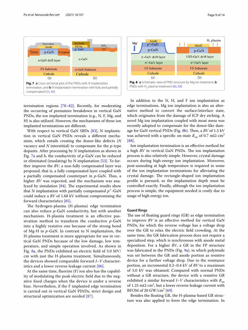
With respect to vertical GaN SBDs [83], N implanta-tion in vertical GaN PNDs reveals a different mecha-nism, which entails creating the donor-like defects (N vacancy and N interstitial) to compensate for the p-type dopants. After processing by N implantation as shown in Fig. 7a and b, the conductivity of p-GaN can be reduced or eliminated (insulating) by N implantation [53]. To fur-ther improve the BV, a non-fully compensated layer was proposed, that is, a fully compensated layer coupled with a partially compensated counterpart in p-GaN. Thus, a higher BV was expected, and the mechanism was ana-lyzed by simulation [84]. The experimental results show that N implantation with partially compensated p+-GaN could induce a BV of 1.68 kV without compromising the forward characteristics [85].
The hydrogen-plasma (H-plasma) edge termination can also reduce p-GaN conductivity, but with another mechanism. H-plasma treatment is an effective pas-sivation method to transform the conductive p-GaN into a highly resistive one because of the strong bond of Mg-H in p-GaN. In contrast to N implantation, the H-plasma treatment is more appropriate for use in ver-tical GaN PNDs because of the low damage, low tem-perature, and simple operation involved. As shown in Fig. 8a, the PNDs exhibited an electric field of 3.0 MV/cm with just the H-plasma treatment. Simultaneously, the devices showed comparable forward I–V character-istics and a lower reverse leakage current [86].
At the same time, fluorine (F) ion also has the capabil-ity of modulating the peak electric field due to the neg-ative fixed charges when the device is under a reverse bias. Nevertheless, if the F implanted edge termination is carried out in vertical GaN PINDs, strict design and structural optimization are needed [87].
In addition to the N, H, and F ion implantation as edge terminations, Mg ion implantation is also an alter-native method to convert the surface/interface state, which originates from the damage of ICP dry etching. A novel Mg ion implantation coupled with moat mesa was recently adopted to compensate for the donor-like dam-age for GaN vertical PNDs (Fig. 8b). Then, a BV of 1.5 kV was achieved with a specific on-state Ron of 0.7 mΩ cm2 [88].
Ion implantation termination is an effective method for a high BV in vertical GaN PNDs. The ion implantation process is also relatively simple. However, crystal damage occurs during high-energy ion implantation. Moreover, post-annealing at high temperature is required in some of the ion implantation terminations for alleviating the crystal damage. The rectangle-shaped ion implantation profile is pursued, so the implantation depth must be controlled exactly. Finally, although the ion implantation process is simple, the equipment needed is costly due to usage of high energy ion.
Guard RingsThe use of floating guard rings (GR) as edge termination to improve BV is an effective method for vertical GaN PNDs, for which the reverse voltage has a voltage drop over the GR to relax the electric field crowding. At the same time, the GR fabrication process does not require a specialized step, which is synchronous with anode metal deposition. For a higher BV, a GR in the FP structure was fabricated in the PNDs (Fig. 9a), in which polyimide was set between the GR and anode portion as resistive device for a further voltage drop. Due to the resistance portion, an incremental 0.2–0.4 kV of BV to a maximum of 5.0 kV was obtained. Compared with normal PNDs without a GR structure, the device with a resistive GR exhibited a similar forward I–V characteristics with Ron of 1.25 mΩ cm2, but a lower reverse leakage current with BFOM of 20 GW/cm2 [69].
Besides the floating GR, the H-plasma-based GR struc-ture was also applied to form the edge termination. In
Fig. 7 a Cross‑sectional plot of the PNDs with N implantation termination, and b N implantation termination with fully and partially compensated [53, 84]
Fig. 8 a Schematic view of PND structure by Mg ion treatment; b PNDs with H2 plasma treatment [86, 88]
Page 10 of 14Pu et al. Nanoscale Res Lett (2021) 16:101
addition to low damage, the low diffusivity of H-plasma could result in relatively ideal profile in GaN [89]. Owing to passivation effect of the H-plasma on p-GaN, the con-ductive p-GaN becomes highly resistive, and the GR structure was subsequently formed by the highly resistive p-GaN ring (Fig. 9b). The narrow GR width of 1–2 µm and decreasing spacing were used to improve the BV. GR structures with varied rings were measured. The PNDs with varied rings have similar forward characteristics with around 0.65 mΩ cm2 and an ideality factor of 1.65 compared with those without GR. More GRs could fur-ther relax the electric field at the device edge. Thus, the devices exhibited a higher BV by increasing the number of rings after measurement. Consequently, the PNDs showed a BV of 1.7 kV with the highest electric field of 3.43 MV/cm 10 GRs [90].
The disadvantage of GR is its low area utilization rate, and the GR structure generally requires a large area, which is even bigger than anode. Then, the amount of GR raises the design difficulty such as the width and spacing of the GR. At present, two and more kinds of edge ter-mination are adopted in single vertical GaN PNDs for a higher BV. These edge terminations typically include the FP, bevel mesa, and guard rings due to the relatively sim-ple fabrications. On the other hand, these edge termina-tions are not meant to introduce the foreign element into the GaN crystal with respect to ion treatment, a feature that is beneficial for device performance. However, the quality of epitaxial layers still occupies a considerable proportion.
Vertical GaN PNDs on Si SubstrateTo date, although vertical GaN-on-GaN devices exhibit excellent performance, the high cost and small diameter of GaN substrates still impede their large-scale market applications. Consider to the merit of a large scale and low cost of Si substrate, GaN-on-Si devices have attracted considerable many attentions at this stage.
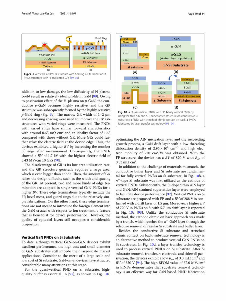
For the quasi-vertical PND on Si substrate, high-quality buffer is essential. In [91], as shown in Fig. 10a,
optimizing the AlN nucleation layer and the succeeding growth process, a GaN drift layer with a low threading dislocation density of 2.95 × 108 cm−2 and high elec-tron mobility of 720 cm2/Vs was obtained. With the FP structure, the device has a BV of 820 V with Ron of 0.33 mΩ cm2.
In addition to the challenge of materials mismatch, the conductive buffer layer and Si substrate are fundamen-tal for fully vertical PNDs on Si substrate. In Fig. 10b, a n+-type Si substrate was first utilized as the cathode of vertical PNDs. Subsequently, the Si-doped thin AlN layer and GaN/AlN strained superlattice layer were employed to facilitate device performance [92]. Vertical PNDs on Si substrate are proposed with FP, and a BV of 288 V is con-firmed with a drift layer of 1.5 µm. Moreover, a higher BV of 720 V in PNDs on Si with 5.7 µm drift layer is reported in Fig. 10c [93]. Unlike the conductive Si substrate method, the cathode ohmic on back approach was made by a trench, which reaches the n+-GaN layer through the selective removal of regular Si substrate and buffer layer.
Besides the conductive Si substrate and trenched ohmic contact on back, substrate removal technology is an alternative method to produce vertical GaN PNDs on Si substrates. In Fig. 10d, a layer transfer technology is used to process vertical PINDs on Si substrate. After Si substrate removal, transfer, n-electrode, and sidewall pas-sivation, the devices exhibit a low Ron of 3.3 mΩ cm2 and BV of 350 V [94]. The high BFOM value of 37.0 MV/cm2 in PINDs demonstrates that substrate removal technol-ogy is an effective way for GaN-based PIND fabrication
Fig. 9 a Vertical GaN PNDs structure with floating GR termination; b PNDs structure with H‑implanted GRs [69, 90]
Fig. 10 a Quasi‑vertical PINDs with FP; b fully vertical PNDs by using the thin AlN and SLS superlattice structure on conductive Si substrate; c PNDs with trenched ohmic contact on back; d PNDs fabricated by layer transfer technology [91–94]
Page 11 of 14Pu et al. Nanoscale Res Lett (2021) 16:101
on Si substrates. Relative to other technologies, however, the more complicated fabrication process and higher production cost are issues that must be addressed during the substrate removal part.
As an alternative technical route, PNDs on Si substrates are fabricated with quasi-vertical or vertical device struc-tures. To mitigate the substantial material mismatch between the Si substrate and GaN epitaxial stacks, a more effective epitaxial technology must be investigated. For a higher BV, thicker drift layer is also essential for a higher BV. This fact presents another key issue to inves-tigate because the drift layer thickness on Si substrate is approximately 5 µm.
Future Challenges and ConclusionVertical PNDs are essential to simultaneously obtain high current (> 100 A) with high voltages (> 600 V), which can meet the requirements of several applications including electric vehicles and recycled energy processing. Despite the great progress achieved, applications of vertical GaN PNDs remain several barriers such as cost and technical limitations.
For FS-GaN substrate, high epitaxial quality with low threading dislocation has been achieved by a common MOCVD. The small size and high cost of the FS-GaN substrate confine the applications of the vertical GaN PNDs within a narrow range, and the small size also raises the price of GaN. The commercial GaN substrate is only 2-inch and is much smaller than 4–6 inch SiC and 8–12 inch Si substrates. The primary challenge for verti-cal GaN PNDs is achieving high epitaxial quality, espe-cially the high quality of the p-GaN layer with a high hole concentration. Recently, novel PNDs are proposed through replacing p-GaN with NiOx synthesized by ther-mal oxidation or sputtering; great performance is also demonstrated as replacement of p-GaN in vertical PND and guard ring in GaN SBD [95–98].
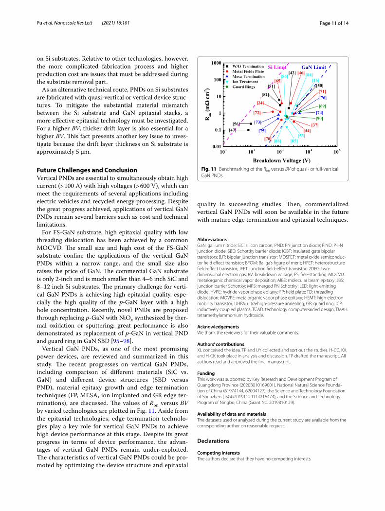
Vertical GaN PNDs, as one of the most promising power devices, are reviewed and summarized in this study. The recent progresses on vertical GaN PNDs, including comparison of different materials (SiC vs. GaN) and different device structures (SBD versus PND), material epitaxy growth and edge termination techniques (FP, MESA, ion implanted and GR edge ter-minations), are discussed. The values of Ron versus BV by varied technologies are plotted in Fig. 11. Aside from the epitaxial technologies, edge termination technolo-gies play a key role for vertical GaN PNDs to achieve high device performance at this stage. Despite its great progress in terms of device performance, the advan-tages of vertical GaN PNDs remain under-exploited. The characteristics of vertical GaN PNDs could be pro-moted by optimizing the device structure and epitaxial
quality in succeeding studies. Then, commercialized vertical GaN PNDs will soon be available in the future with mature edge termination and epitaxial techniques.
AbbreviationsGaN: gallium nitride; SiC: silicon carbon; PND: PN junction diode; PIND: P‑i‑N junction diode; SBD: Schottky barrier diode; IGBT: insulated gate bipolar transistors; BJT: bipolar junction transistor; MOSFET: metal oxide semiconduc‑tor field effect transistor; BFOM: Baliga’s figure of merit; HFET: heterostructure field‑effect transistor; JFET: junction field‑effect transistor; 2DEG: two‑dimensional electron gas; BV: breakdown voltage; FS: free‑standing; MOCVD: metalorganic chemical vapor deposition; MBE: molecular beam epitaxy; JBS: junction barrier Schottky; MPS: merged PN Schottky; LED: light‑emitting diode; HVPE: hydride vapor phase epitaxy; FP: field plate; TD: threading dislocation; MOVPE: metalorganic vapor phase epitaxy; HEMT: high electron mobility transistor; UHPA: ultra‑high‑pressure annealing; GR: guard ring; ICP: inductively coupled plasma; TCAD: technology computer‑aided design; TMAH: tetramethylammonium hydroxide.
AcknowledgementsWe thank the reviewers for their valuable comments.
Authors’ contributionsXL conceived the idea. TP and UY collected and sort out the studies. H‑CC, KX, and H‑CK took place in analysis and discussion. TP drafted the manuscript. All authors read and approved the final manuscript.
FundingThis work was supported by Key Research and Development Program of Guangdong Province (2020B010169001), National Natural Science Founda‑tion of China (61974144, 62004127), the Science and Technology Foundation of Shenzhen (JSGG20191129114216474), and the Science and Technology Program of Ningbo, China (Grant No. 2019B10129).
Availability of data and materialsThe datasets used or analyzed during the current study are available from the corresponding author on reasonable request.
Declarations
Competing interestsThe authors declare that they have no competing interests.
101 102 103 104 1050.01
0.1
1
10
100
1000
.
Si Limit
[37][90][74]
[69]
[76][71]
[50][16]
[84][46][42]
[65][51]
[52]
[24]
[72]
[73]
[75]
[70] [88]
[44][53]
[85]
[56][47]
W/O Termination Metal Fields Plate Mesa Termination Ion Treatment Guard Rings
Ron
(mΩΩ
cm
2 )
Breakdown Voltage (V)
[86]
GaN Limit
Fig. 11 Benchmarking of the Ron versus BV of quasi‑ or full‑vertical GaN PNDs
Page 12 of 14Pu et al. Nanoscale Res Lett (2021) 16:101
Author details1 College of Materials Science and Engineering, Shenzhen University–Hanshan Normal University Postdoctoral Workstation, Shenzhen University, Shenz‑hen 518060, China. 2 Key Laboratory of Optoelectronic Devices and Systems of Ministry of Education and Guangdong Province, College of Physics and Optoelectronic Engineering, Shenzhen University, Shenzhen 518060, China. 3 Department of Electronic Engineering, Chang Gung University, Taoyuan 333, Taiwan. 4 Suzhou Institute of Nano‑Tech and Nano‑Bionics, Chinese Academy of Sciences, Suzhou 215123, China. 5 Photonic and Institute of Electro‑Optical Engineering, National Chiao Tung University, Hsinchu 300, Taiwan.
Received: 30 March 2021 Accepted: 20 May 2021
References 1. Zhang Y, Dadgar A, Palacios T (2018) Gallium nitride vertical power
devices on foreign substrates: a review and outlook. J Phys D Appl Phys 51(27):273001
2. Sheng K, Williams BW, Finney SJ (2000) A review of IGBT models. IEEE Trans Power Electron 15(6):1250–1266
3. Carrasco JM, Franquelo LG, Bialasiewicz JT, Galvan E, PortilloGuisado RC, Parts MAM, Leon JJ, Moreno‑Alfonso N (2006) Power‑electronic systems for the grid integration of renewable energy sources: a survey. IEEE Trans Power Electron 53(4):1002–1016
4. Fujita S (2015) Wide‑bandgap semiconductor materials: for their full bloom. Jpn J Appl Phys 54(3):030101
5. Higashiwaki M, Sasaki K, Murakami H, Kumagai Y, Koukitu A, Kuramata A, Masui T, Yamakoshi S (2016) Recent progress in Ga2O3 power devices. Semicond Sci Technol 31(3):034001
6. Kaminski N, Hilt O (2014) SiC and GaN devices–wide bandgap is not all the same. IET Circuits Devices Syst 8(3):227–236
7. Ueda T (2014) Reliability issues in GaN and SiC power devices. In: 2014 IEEE international reliability physics symposium
8. Rohm Semiconductor Co (2013) SiC power devices and modules. Rohm Semiconductor Co., Appl. Note 13103EAY01
9. Kimoto T (2015) Material science and device physics in SiC technology for high‑voltage power devices. Jpn J Appl Phys 54(4):040103
10. Dang K, Zhang J, Zhou H, Yin S, Zhang T, Ning J, Zhang Y, Bian Z, Chen J, Duan X, Zhao S, Hao Y (2019) Lateral GaN Schottky barrier diode for wireless high‑power transfer application with high RF/DC conversion efficiency: from circuit construction and device technologies to system demonstration. IEEE Trans Ind Electron 67(8):6597–6606
11. Zheng X, Tang Z, Lv L, Bai D, Wang C, Mao W, Cao Y, Ma X, Hao Y (2019) A novel AlGaN/GaN Schottky barrier diode with partial p‑AlGaN cap layer and recessed dual‑metal anode for high breakdown and low turn‑on voltage. Semicond Sci Technol 35(1):015018
12. Liang S, Song X, Zhang L, Lv Y, Wang Y, Wei B, Guo Y, Gu G, Wang B, Cai S, Feng Z (2020) A 177–183 GHz high‑power GaN‑based frequency doubler with over 200 mW output power. IEEE Electron Device Lett 41(5):669–672
13. Zhang T, Zhang J, Zhou H, Wang Y, Chen T, Zhang K, Zhang Y, Dang K, Bian Z, Zhang J, Xu S, Duan X, Ning J, Hao Y (2019) A>3 kV/2.94 mΩ·cm2 and low leakage current with low turn‑on voltage lateral GaN Schottky barrier diode on silicon substrate with anode engineering technique. IEEE Electron Device Lett 40(10):1583–1586
14. Dang K, Zhang J, Zhou H, Huang S, Zhang T, Bian Z, Zhang Y, Wang X, Zhao S, Wei K, Hao Y (2019) A 58 GHz high‑power and high‑efficiency rec‑tifier circuit with lateral GaN Schottky diode for wireless power transfer. IEEE Trans Power Electron 35(3):2247–2252
15. Shinohara K, Regan DC, Tang Y, Corrion AL, Brown DF, Wong JC, Robinson JF, Fung H, Schmitz A, Oh TC, Kim S, Chen PS, Nagele RG, Margomenos AD, Micovic M (2013) Scaling of GaN HEMTs and Schottky diodes for submillimeter‑wave MMIC applications. IEEE Trans Electron Devices 60(10):2982–2996
16. Kizilyalli IC, Edwards AP, Aktas O, Prunty T, Bour D (2015) Vertical power p–n diodes based on bulk GaN. IEEE Trans Electron Devices 62(2):414–422
17. Gu H, Tian F, Zhang C, Xu K, Wang J, Chen Y, Deng X, Liu X (2019) Recov‑ery performance of Ge‑doped vertical GaN Schottky barrier diodes. Nanoscale Res Lett 14(40):2872
18. Liu X, Liu Q, Li C, Wang J, Yu W, Xu K, Ao J‑P (2017) 1.2kV GaN Schottky barrier diodes on free‑standing GaN wafer using a CMOS‑compatible contact material. Jpn J Appl Phys 56(2):026501
19. Oka T (2019) Recent development of vertical GaN power devices. Jpn J Appl Phys 58(SB):SB0805
20. Zhang Y (2020) Comparison between competing requirements of GaN and SiC family of power switching devices. In: 2020 IOP conference series: materials science and engineering, 738:012004
21. Zhang Y, Sun M, Liu Z, Piedra D, Lee H‑S, Gao F, Fujishima T, Palacios T (2013) Electrothermal simulation and thermal performance study of GaN vertical and lateral power transistors. IEEE Trans Electron Devices 60(7):2224–2230
22. Disney D, Nie H, Edwards A, Bour D, Shah H, Kizilyalli IC (2014) Vertical power diodes in bulk GaN. In: 2013 25th International symposium on power semiconductor devices & IC’s (ISPSD)
23. Yates L, Anderson J, Gu X, Lee C, Bai T, Mechienburg M, Aoki T, Goorsky MS, Kuball M, Piner EL, Graham S (2018) Low thermal boundary resist‑ance interfaces for GaN‑on‑diamond devices. ACS Appl Mater Interfaces 10(28):24302–24309
24. Nomoto K, Hatakeyama Y, Katayose H, Kaneda N, Mishima T, Nakamura T (2011) Over 1.0 kV GaN p–n junction diodes on free‑standing GaN substrates. Phys Stat Sol (a) 208(7):1535–1537
25. Sun Y, Kang X, Zheng Y, Lu J, Tian X, Wei K, Wu H, Wang W, Liu X, Zhang G (2019) Review of the recent progress on GaN‑based vertical power Schottky barrier diodes (SBDs). Electronics 8(5):575
26. Amano H, Baines Y, Beam E, Borga M, Bouchet T, Chalker P, Charles M, Chen KJ, Chowdhury N, Chu R et al (2018) The 2018 GaN power electron‑ics roadmap. J Phys D Appl Phys 51(16):163001
27. Han S, Yang S, Li R, Wu X, Sheng K (2018) Current‑collapse‑free and fast reverse recovery performance in vertical GaN‑on‑GaN Schottky barrier diode. IEEE Trans Power Electron 34(6):5012–5018
28. Xu R, Chen P, Liu M, Zhou J, Yang Y, Li Y, Ge C, Peng H, Liu B, Chen D, Xie Z, Zhang R, Zheng Y (2020) 1.4‑kV quasi‑vertical GaN Schottky barrier diode with reverse p–n junction termination. IEEE J Electron Devices Soc 8:316–320
29. Kizilyalli IC, Edwards AP, Nie H, Quang PB, Disney D, Bour D (2014) 400‑A (Pulsed) vertical GaN p–n diode with breakdown voltage of 700 V. IEEE Electron Device Lett 35(6):654–656
30. Yin R, Li Y, Wen CP, Fu Y, Hao Y, Wang M, Shen B (2020) High voltage verti‑cal GaN‑on‑GaN Schottky barrier diode with high energy fluorine ion implantation based on space charge induced field modulation (SCIFM) effect. In: 2020 IEEE 32nd international symposium on power semicon‑ductor devices and ICs (ISPSD)
31. Yang T, Fu H, Fu K, Yang C, Montes J, Huang X, Chen H, Zhou J, Qi X, Deng X, Zhao Y (2020) Vertical GaN‑on‑GaN Schottky barrier diodes with multi‑floating metal rings. IEEE J Electron Devices Soc 8:857–863
32. Liang S, Fang Y, Xing D, Zhang Z, Wang J, Guo H, Zhang L, Gu G, Feng Z (2016) GaN planar Schottky barrier diode with cut‑off frequency of 902 GHz”. Electron Lett 52(16):1408–1410
33. Dmitriev VA, Irvine KG, Carter CH (1998) Electric breakdown in GaN p–n junctions. Appl Phys Lett 68(2):229
34. Nie K, Xu W, Ren F, Zhou D, Pan D, Ye J, Chen D, Zhang R, Zheng Y, Lu H (2020) Highly enhanced inductive current sustaining capability and ava‑lanche ruggedness in GaN p‑i‑n diodes with shallow bevel termination. IEEE Electron Device Lett 41(3):469–472
35. Zhang Y, Lu X, Zou X (2019) Device design assessment of GaN merged P‑i‑N Schottky diodes, vertical GaN junction barrier Schottky diodes. Electronics 8(12):1550
36. Kuksenkov DV, Temkin H (1998) Low‑frequency noise and performance of GaN p–n junction photodetectors. J Appl Phys 83(4):2142
37. Nomoto K, Song B, Hu Z, Zhu M, Qi M, Kaneda N, Mishima T, Nakamura T, Jena D, Xing HG (2015) 1.7 kV and 0.55 mΩ·cm2 GaN p–n diodes on bulk GaN substrates with avalanche capability. IEEE Electron Device Lett 37(2):161–164
38. Kizilyalli IC, Quang PB, Disney D, Bhatia H, Aktas O (2015) Reliability stud‑ies of vertical GaN devices based on bulk GaN substrates. Microelectron Reliabil 55(9):1654
39. Molnar RJ, Nichols KB, Maki P, Brown ER, Melngailis I (1995) The role of impurities in hydride vapor phase epitaxially grown gallium nitride. MRS Proc 378:479
Page 13 of 14Pu et al. Nanoscale Res Lett (2021) 16:101
40. Oshima Y, Eri T, Shibata M, Sunakawa H, Usui A (2002) Fabrication of free‑standing GaN wafers by hydride vapor‑phase epitaxy with void‑assisted separation. Phys Stat Sol (a) 194(2):554–558
41. Gu H, Ren G, Zhou T, Tian F, Xu Y, Zhang Y, Wang M, Wang J, Xu K (2015) The electrical properties of bulk GaN crystals grown by HVPE. J Cryst Growth 436:76–81
42. Fujikura H, Hayashi K, Horikiri F, Narita Y, Konno T, Yoshida T, Ohta H, Mishima T (2018) Elimination of macrostep‑induced current flow nonu‑niformity in vertical GaN PN diode using carbon‑free drift layer grown by hydride vapor phase epitaxy. Appl Phys Exp 11(4):045502
43. Bliss D, Wang B, Suscavage M, Lancto R, Swider S, Eikenberry W, Lynch C (2010) Ammonothermal GaN: morphology and properties. J Cryst Growth 312(8):1069–1073
44. Chen SWH, Wang HY, Hu C, Chen Y, Wang H, Wang J, He W, Sun X, Chiu HC, Kuo H, Wang W, Xu K, Li D, Liu XK (2019) Vertical GaN‑on‑GaN PIN diodes fabricated on free‑standing GaN wafer using an ammonothermal method. J Alloys Compds 804:435–440
45. Wienecke S, Romanczyk B, Guidry M, Li H, Zheng X, Ahmadi E, Hestroffer K, Megalini L, Keller S, Mishra UK (2016) N‑Polar deep recess MISHEMTs with record 2.9 W/mm at 94 GHz. IEEE Electron Device Lett 37(6):713
46. Liu X, Chiu HC, Wang HY, Hu C, Wang HC, Kao HL, Chien FT (2018) 2.4 kV vertical GaN PN diodes on free standing GaN wafer using CMOS‑compat‑ible contact materials. IEEE J Electron Devices Soc 6:825–829
47. Cho YJ, Hu Z, Nomoto K, Xing HG, Jena D (2017) Single‑crystal N‑polar GaN p‑n diodes by plasma‑assisted molecular beam epitaxy. Appl Phys Lett 110(25):253506
48. Fu H, Zhang X, Fu K, Liu H, Alugubelli SR, Huang X, Chen H, Baranow‑ski I, Yang TH, Xu K (2018) Nonpolar vertical GaN‑on‑GaN p–n diodes grown on free‑standing (1010) m‑plane GaN substrates. Appl Phys Exp 11(11):111003
49. Kozodoy P, Ibbetson JP, Marchand H, Fini PT, Keller S, Speck JS, DenBaars SP, Mishra UK (1998) Electrical characterization of GaN p–n junctions with and without threading dislocations. Appl Phys Lett 73(7):975–977
50. Kizilyalli IC, Prunty T, Aktas O (2015) 4 kV and 28 mΩ·cm2 Vertical GaN p–n diodes with low leakage currents. IEEE Electron Device Lett 36(10):1073–1075
51. Yoshizumi Y, Hashimoto S, Tanabe T, Kiyama M (2007) High‑break‑down‑voltage pn‑junction diodes on GaN substrates. J Cryst Growth 298:875–878
52. Fu H, Huang X, Chen H, Lu Z, Zhang X, Zhao YJ (2017) Effect of buffer layer design on vertical GaN‑on‑GaN p–n and Schottky power diodes. IEEE Electron Device Lett 38(6):763–766
53. Han S, Yang S, Li Y, Liu Y, Sheng K (2019) Photon‑enhanced conductivity modulation and surge current capability in vertical GaN power rectifiers. In: 2019 31st International symposium on power semiconductor devices and ICs (ISPSD). IEEE, pp 63–66
54. Yoshino M, Horikiri F, Ohta H, Yamamoto Y, Mishima T, Nakamura T (2016) High‑k dielectric passivation for GaN diode with a field plate termination. Electron 5(2):15
55. Cao XA, Lu H, LeBoeuf SF, Cowen C, Arthur SD (2005) Growth and char‑acterization of GaN PiN rectifiers on free‑standing GaN. Appl Phys Lett 87(5):053503
56. Qi M, Nomoto K, Zhu M, Hu Z, Zhao Y, Protasenko V, Song B, Yan X, Li G, Verma J, Bader S, Fay P, Xing HG, Jena D (2015) High breakdown single‑crystal GaN p–n diodes by molecular beam epitaxy. Appl Phys Lett 107(23):232101
57. Maruska HP, Tietjen JJ (1969) The preparation and properties of vapor‑deposited single‑crystal‑line GaN. Appl Phys Lett 15(10):327–329
58. Amano H, Kito M, Hiramatsu K, Akasaki I (1989) P‑type conduction in Mg‑doped GaN treated with low‑energy electron beam irradiation (LEEBI). Jpn J Appl Phys 28(12):L2112–L2114
59. Posthuma NE, You S, Liang H, Ronchi N, Kang X, Wellekens D, Saripalli YN, Decoutere S (2016) Impact of Mg out‑diffusion and activation on the p‑GaN gate HEMT device performance. In: 2016 28th International symposium on power semiconductor devices and ICs (ISPSD). IEEE, pp. 95–98
60. Nakamura S, Mukai T, Senoh M, Iwasa N (1992) Thermal annealing effects on P‑type Mg‑doped GaN films. Jpn J Appl Phys 31(28):L139–L142
61. Kuo CH, Chang SJ, Su YK, Wu LW, Sheu JK, Chen CH, Chi GC (2002) Low temperature activation of Mg‑doped GaN in O2 ambient. Jpn J Appl Phys 41(2A):L112
62. Nakamura S, Iwasa N, Senoh M, Mukai T (1992) Hole compensation mechanism of p‑type GaN films. Jpn J Appl Phys 31(5R):1258–1266
63. Kaufmann U, Schlotter P, Obloh H, Kohler K, Maier M (2000) Hole conductivity and compensation in epitaxial GaN: Mg layers. Phys Rev B 62(16):10867
64. Kozodoy P, Xing H, DenBaars SP, Mishra UK (1999) Heavy doping effects in Mg‑doped GaN. J Appl Phys 87(4):1832–1835
65. Hu Z, Nomoto K, Qi M, Li W, Zhu M, Gao X, Jena D, Xing HG (2017) 1.1 kV vertical GaN p–n diodes with p‑GaN regrown by molecular beam epitaxy. IEEE Electron Device Lett 38(8):1071–1074
66. Sakurai H, Omori M, Yamada S, Furukawa Y, Suzuki H, Narita T, Kataoka K, Horita M, Bockowski M, Suda J, Kachi T (2019) Highly effective activa‑tion of Mg‑implanted p‑type GaN by ultra‑high‑pressure annealing. Appl Phys Lett 115(14):142104
67. Kumta A, Tin CC, Ahn J (2006) Design of field‑plate terminated 4H‑SiC Schottky diodes using high‑k dielectrics. Microelectron Reliab 46(8):1295–1302
68. Ikeda K, Umezawa H, Shikata S (2008) Edge termination techniques for p‑type diamond Schottky barrier diodes. Diam Relat Mater 17(4–5):809–812
69. Ohta H, Hayashi K, Horikiri F, Yoshino M, Nakamura T, Mishima T (2018) 5.0 kV breakdown‑voltage vertical GaN p–n junction diodes. Jpn J Appl Phys 57(4):04FG09
70. Hatakeyama Y, Nomoto K, Kaneda N, Kawano T, Mishima T, Naka‑mura T (2011) Over 3.0 GW/cm2 figure‑of‑merit GaN p–n junction diodes on free‑standing GaN substrates. IEEE Electron Device Lett 32(12):1674–1676
71. Hatakeyama Y, Nomoto K, Terano A, Kaneda N, Tsuchiya T, Mishima T, Nakamura T (2013) High‑breakdown‑voltage and low‑specific‑on‑resistance GaN p–n junction diodes on free‑standing GaN substrates fabricated through low‑damage field‑plate process. Jpn J Appl Phys 52(28):028007
72. Ueoka Y, Deki M, Honda Y, Amano H (2018) Improvement of break‑down voltage of vertical GaN p–n junction diode with Ga2O3 pas‑sivated by sputtering. Jpn J Appl Phys 57(7):070302
73. Fukushima H, Usami S, Ogura M, Ando Y, Tanaka A, Deki M, Kushimoto M, Nitta S, Honda Y, Amano H (2019) Vertical GaN pn diode with deeply etched mesa and capability of avalanche breakdown. Appl Phys Exp 12:026502
74. Ohta H, Asai N, Horikiri F, Narita Y, Yoshida T, Mishima T (2019) Two‑step mesa structure GaN p–n diodes with low ON‑resistance, high breakdown voltage, and excellent avalanche capabilities. IEEE Electron Device Lett 41(1):123–126
75. Yu CJ, Lu JY, Shan LW, Chen CJ, Liao JH, Wu MC (2019) Over 1 GW/cm2 for high‑power GaN p‑i‑n diodes with edge termination structure and laser annealing. J Vac Sci Technol B 37(1):011208
76. Nomoto K, Hu Z, Song B, Zhu M, Qi M, Yan R, Protasenko V, Imhoff E, Kuo J, Kaneda N, Mishima T, Nakamura T, Jena D, Xing HG (2015) GaN‑on‑GaN p–n power diodes with 3.48 kV and 0.95 mΩ·cm2: a record high figure‑of‑merit of 12.8 GW/cm2. In: 2015 IEEE international electron devices meeting (IEDM)
77. Maeda T, Narita T, Ueda H, Kanechika M, Uesugi T, Kachi T, Kimoto T, Horita M, Suda J (2019) Design and fabrication of GaN p–n junction diodes with negative beveled‑mesa termination. IEEE Electron Device Lett 40(6):941–944
78. Ozbek AM, Baliga BJ (2011) Planar nearly ideal edge‑termination tech‑nique for GaN devices. IEEE Electron Device Lett 32(3):300–302
79. Shiu J, Huang J, Desmaris V, Chang C, Lu C, Kumakura K, Makimoto T, Zirath H, Rorsman N, Chang EY (2011) Oxygen ion implantation isola‑tion planar process for AlGaN/GaN HEMTs. IEEE Electron Device Lett 28(6):476–478
80. Jiang Y, Wang Q, Zhang F, Li L, Shinkai S, Wang D, Ao J (2016) Improve‑ment of device isolation using field implantation for GaN MOSFETs. Semicond Sci Technol 31(3):035019
81. Nie H, Edwards AP, Disney DR, Brown RJ, Kizilyalli IC (2014) Method and system for junction termination in GaN materials using conductivity modulation. U.S. patent application 8716716B2
82. Laroche JR, Ren F, Baik KW, Pearton SJ, Shelton BS, Peres B (2005) Design of edge termination for GaN power Schottky diodes. J Electron Mater 34:370–374

Page 14 of 14Pu et al. Nanoscale Res Lett (2021) 16:101
83. Han S, Yang S, Sheng K (2018) High‑voltage and high‑ION/IOFF vertical GaN‑on‑GaN Schottky barrier diode with nitridation‑based termination. IEEE Electron Device Lett 39(4):572–575
84. Dickerson JR, Allerman AA, Bryant BN, Fischer AJ, King MP, Moseley MW, Armstrong AM, Kaplar RJ, Kizilyalli IC, Aktas O, Werer JJ (2016) Vertical GaN power diodes with a bilayer edge termination. IEEE Trans Electron Devices 63(1):419–425
85. Wang J, Cao L, Xie J, Beam E, McCarthy R, Youtsey C, Fay P (2018) High voltage, high current GaN‑on‑GaN p‑n diodes with partially compen‑sated edge termination. Appl Phys Lett 113(2):023502
86. Ji D, Li S, Ercan B, Ren C, Chowdhury S (2019) Design and fabrication of ion‑implanted moat etch termination resulting in 0.7 mΩ·cm2/1500 V GaN Diodes. IEEE Electron Device Lett 41(2):264–267
87. Liu Y, Yang S, Sheng K (2020) Design and optimization of vertical GaN PiN diodes with fluorine‑implanted termination. IEEE J Electron Devices Soc 8:241–250
88. Fu H, Fu K, Huang X, Chen H, Baranowski I, Yang TH, Montes J, Zhao Y (2018) High performance vertical GaN‑on‑GaN p–n power diodes with hydrogen‑plasma‑based edge termination. IEEE Electron Device Lett 39(7):1018–1021
89. Götz W, Johnson NM, Walker J, Bour DP, Amano H, Akasaki I (2005) Hydro‑gen passivation of Mg acceptors in GaN grown by metalorganic chemical vapor deposition. Appl Phys Lett 67(18):2666
90. Fu H, Fu K, Alugubelli SR, Cheng CY, Huang X, Chen H, Yang TH, Yang C, Zhou J, Montes J, Deng X, Qi X, Goodnick SM, Ponce FA, Zhao YJ (2019) High voltage vertical GaN p–n diodes with hydrogen‑plasma based guard rings. IEEE Electron Device Lett 41(1):127–130
91. Khadar RA, Liu C, Zhang L, Xiang P, Cheng K, Matioli E (2018) 820 V GaN‑on‑Si quasi‑vertical p‑i‑n diodes with BFOM of 2.0 GW/cm2. IEEE Electron Device Lett 39(3):401–404
92. Mase S, Urayama Y, Hamada T, Freedsman JJ, Egawa T (2016) Novel fully vertical GaN p–n diode on Si substrate grown by metalorganic chemical vapor deposition. Appl Phys Lett 9(11):111005
93. Zhang Y, Yuan M, Chowdhury N, Cheng K, Palacios T (2016) 720 V/0.35 mΩ·cm2 fully‑vertical GaN‑on‑Si power diodes by selective removal of Si substrates and buffer layers. IEEE Electron Device Lett 39(5):715–718
94. Zou X, Zhang X, Lu X, Tang CW, Lau KM (2016) Fully vertical GaN p‑i‑n diodes using GaN‑on‑Si Epilayers. IEEE Electron Device Lett 37(5):636–639
95. Li X, Pu T, Zhang T, Li X, Li L, Ao J‑P (2020) p‑NiO/n‑GaN heterostructure diode for temperature sensor application. IEEE Sens J 20(1):62–66
96. Wang Y, Pu T, Li X, Li L, Ao J‑P (2021) Application of p‑type NiO deposited by magnetron reactive sputtering on GaN vertical diodes. Mater Sci Semi‑cond Proc 125:105628
97. Zhou J, He L, Li X, Pu T, Li L, Ao J‑P (2021) Vertical GaN Schottky barrier diodes with area‑selectively deposited p‑NiO guard ring termination structure. Superlattices Microstruct 151:106820
98. Li L, Wang X, Liu Y, Ao J‑P (2015) NiO/GaN heterojunction diode deposited through magnetron reactive sputtering. J Vac Sci Technol A 34(2):02D104
Publisher’s NoteSpringer Nature remains neutral with regard to jurisdictional claims in pub‑lished maps and institutional affiliations.