Embed Size (px)
Citation preview

Review of ATLAS Simulation Tools
151
Appendix A
REVIEW OF ATLAS
SIMULATION TOOLS
A.1 Overview of ATLAS
ATLAS provides general capabilities for physically-based two dimensional (2D)
simulation tools of semiconductor devices. It predicts the electrical behavior of
specified semiconductor structures and provides insight into the internal physical
mechanisms associated with device operation.
It is designed to be used with the virtual wafer fabrication (VWF) interactive
tools. The VWF interactive tools are DECKBUILD and TONYPLOT. An ATLAS
command file is a list of commands for ATLAS to execute. This list is stored as an
ASCII text file that can be prepared in DECKBUILD or in any text editor. Preparing
an input file in DECKBUILD is preferred. The input file contains a sequence of
statements. Each statement consists of a keyword that identifies the statement and a
set of parameters. ATLAS can read up to 256 characters on one line. But it is better
to spread long input statements over several lines to make the input file more
readable. The “\” character at the end of a line indicates continuation.
A.2 ATLAS Input/Output Files
Fig A.1 shows the types of information that flow from input to output of ATLAS.
Most ATLAS simulations use two input files. The first input file is a text file that
contains commands for ATLAS to execute. The second input file is a structure file
that defines the structure that will be simulated.

Review of ATLAS Simulation Tools
152
This tool produces three types of output files. The first type of output file is the
run-time output, which gives the progress, error and warning messages as the
simulation proceeds. The second type of output file is the log file, which stores all
terminal voltages and currents from the device analysis. The third type of output file
is the solution file, which stores 2D data relating to the values of solution variables
within the device at a given bias point.
Figure A.1: ATLAS input/output files [A.1].
A.3 Order of ATLAS Commands
The order in which statements occur in an ATLAS input file is important. These
are five groups of statements that must occur in the correct order (see Fig.A.2).
Otherwise, an error message will appear, which may cause incorrect operation or
termination of the program. For example, if the material parameters or models are set
in the wrong order, then they may not be used in the calculations. The order of
statements within the mesh definition, structural definition, and solution groups is
also important. Otherwise, it may also cause incorrect operation or termination of the
program [A.1].

Review of ATLAS Simulation Tools
153
Figure A.2: ATLAS commands group with the primary statements in each group.
A.4 ATLAS Commands Syntax
The input file contains a sequence of statements. Each statement consists of a
keyword that indentifies the statement and set of parameters. The general format is:
<STATEMENT> <PARAMETER> <VALUE>
With a few exceptions, the input syntax is not case sensitive. There are some
commands described in this tool as being executed by DECKBUILD is case
sensitive. These include EXTRACT, SET, GO and SYSTEM. Also filenames for
input and output are case sensitive.
A.4.1 Defining a structure
The first statement must be
Specification
Mesh
generation
Region
Assignment
Electrode
Assignment
Doping
profile
Contact
name
Material
Assignment
Parameter
extraction
Structure for
different bias
Plot of
graph
1. Structure Specification
2. Material Model
specification
3. Numerical method selection
4. Solution Specification
5. Results Analysis
Start
End
Review of ATLAS Simulation Tools
154
MESH SPACE.MULT =<value>
This is followed by a series of X.MESH and Y.MESH statements such as:
X.MESH location =<value> spacing =<value>
Y.MESH location =< value> spacing =< value>
The SPACE.MULT parameter value is used as a scaling factor for the mesh created
by the X.MESH and Y.MESH statements. The defaults value is 1. Values greater
than 1 will create a globally coarser mesh for fast simulation. Values less than 1 will
create a globally finer mesh for increased accuracy. The X.MESH and Y.MESH
statements are used to specify the locations in microns of vertical and horizontal
lines, respectively.
A.4.2 Specifying regions and materials
Once the mesh is specified, every part of it must be assigned a region and each
region a material type. This is done with REGION statement. For example:
REGION numbers=<integer> < material type> < position parameters>
Region numbers must start at 1 and are increased for each subsequent region
statement. You can have up to 200 different regions in ATLAS. A large number of
materials is available. If a composition material type is defined, the X and Y
composition fractions can also be specified in the REGION statement.
The position parameters of regions are specified in microns using the X.MIN,
X.MAX, Y.MIN, and Y.MAX parameters. If the position parameters of a new
statement overlapped with previous REGION statement, the overlapped area is need
to be assigned the new region and new material type, otherwise a error messages will
appear and ATLAS won’t run successfully. Furthermore, the MATERIAL statement
is used to specify the material properties in the defined regions.
A.4.3 Specifying electrode
Once the regions and materials have been specified, define at least one electrode
that contacts a semiconductor material. This is done with the ELECTRODE
statement. For example:
Electrode name = <electrode name> < position_parameters>

Review of ATLAS Simulation Tools
155
Maximum 50 electrodes can specify. The position parameters are specified in
microns using the X.MIN, X.MESH, Y.MIN, and Y.MAX parameters. Multiple
electrode statements may have the same electrode name. Nodes that are associated
with the same electrode name are treated as being electrically connected.
A.4.4 Specifying doping
The analytical doping distributions can be specified in deckbuild and the syntax
of the DOPING statement is given as below:
DOPING < distribution _type > < dopant_type> < position_parametrs >
Analytical doping profiles can have uniform or Gaussian forms. The parameters
defining the analytical distribution are specified in the DOPING statement and
position parameters X.MIN, X.MAX , Y.MIN, Y.MAX and Y.MAX can be used
instead of a region number.
A.4.5 Defining material parameters and models
Once the mesh, geometry, and doping profiles are defined, program can modify
the characteristics of electrodes, change the default material parameters, and choose
which physical models ATLAS will use during the device simulation. To accomplish
these actions, use the CONTACT, MATERIAL, and MODELS statements
respectively. Impact ionization models can be enabled using the IMPACT statement.
Interface properties are set by using the INTERFACE statement [1].
An electrode in contact with semiconductor material is assumed by default to be
ohmic. If a work function is defined, the electrode is treated as a Schottky contact.
The CONTACT statement is used to specify the metal work function of one or more
electrodes. The NAME parameters is used to identify in which electrode will have its
modified properties. Physical models are specified using the MODELS and IMPACT
statements. Parameters for these models appear on many statements including:
MODELS, IMPACT, MOBILITY, and MATERIAL, the physical models can be
grouped into five classes: mobility, recombination, and carrier statistics, impact
ionization, and tunneling. Several different numerical methods can be used for
calculating the solutions to semiconductor device problems.

Review of ATLAS Simulation Tools
156
Numerical methods can be written in the METHOD statements of the input file.
Different combinations of models will appear ATLAS to solve up to six equations.
For each of the model types , there are basically three types of solutions technique :
(a) decoupled GUMMEL, (b) fully coupled NEWTON and (c) BLOCK. The
GUMMEL, method will solve for each unknown in turn keeping the other variables
constant, repeating the process until a stable solution is achieved. The NEWTON
method solves the total system of unknowns together. The BLOCK methods will
solve some equations fully coupled while others are decoupled.
A.5 Obtaining Solutions
ATLAS can calculate DC, AC small-signal, and transient solutions. Obtaining
solutions is similar to setting up parametric test equipment for device tests. You
usually define the voltages on each of the electrodes in the device. ATLAS then
calculates the current through each electrode. ATLAS also calculates internal
quantities, such as carrier concentrations and electric fields throughout the device.
This information is very important for getting the internal device status [A.2].
A.5.1 DC solution
In DC solution, the voltage on each electrode is specified using the SOLVE
statement. For example, the statements:
SOLVE VGATE=0.2
SOLVE VGATE=0.4
solves a single bias point with 0.2V and then 0.4V on the gate electrode. One
important rule in ATLAS is that when the voltage on any electrode is not specified in
a given SOLVE statement, the value from the last SOLVE statement is assumed
A.5.2 Small-signal AC solution
Specifying AC simulations is a simple extension of the DC solution syntax.
AC small-signal analysis is performed as a post-processing operation to a DC

Review of ATLAS Simulation Tools
157
solution. The results of AC simulations are the conductance and capacitance between
each pair of electrodes [A.3].
A.5.3 Parameter extractions
The EXTRACT command is provided within the DECKBUILD environment. It
allows you to extract device parameters. The command has a flexible syntax that
allows users to construct specific EXTRACT routines. EXTRACT operates on the
previous solved curve or structure file. By default, EXTRACT uses the currently
open log file. To override this default, supply the name of a file to be used by
EXTRACT before the extraction routine, i.e.:
EXTRACT INIT INF="<filename>"
A.6 Mixed mode Device and Circuit Simulations
Mixed modde is a circuit simulator that can include elements simulated using
device simulation and compact circuit models. It combines different levels of
abstraction to simulate relatively small circuits where compact models for single
devices are unavailable or sufficiently accurate. Mixed mode also allows once to do
multi-device simulations. It uses advanced numerical algorithms that are efficient and
robust for DC, transient, small-signal AC and small-signal network analysis.
Mixed mode circuits can include up to 200 nodes, 300 elements, and up to ten
numerical simulated ATLAS devices. These limits are reasonable for most
applications. The circuit elements that are supported include dependent and
independent voltage and current sources as well as resistors, capacitors, inductors,
coupled inductors, MOSFETs, BJTs, diodes, and switches. The SPICE input
language is used for circuit specification.
A.6.1 General Syntax rule
The SPICE-like part of any mixed mode input file starts with the .BEGIN
statement. The SPICE-like part of the input file ends with .END. All parameters
related to the device simulation models appear after the .END statement [A.1][A.3].

Review of ATLAS Simulation Tools
158
The SPICE-like mixed mode statements can be divided into three categories:
Ø Element Statements: These statements define the circuit netlist. Each device in
the circuit is described by an element statement. The element statement contains
the element name, the circuit nodes to which the element is connected and the
values of the element parameters. The first letter of an element name specifies the
type of element to be simulated. i.e., a resistor name must begin with the letter, R,
and can contain one or more characters.
Ø Simulation Control Statements: These statements specify the analysis to be
performed in mixed mode. These take the place of the SOLVE statements in a
regular ATLAS input file. At least one of these statements must appear in each
mixed mode input file. These statements are:
DC : Steady state analysis including loops.
TRAN : Transient analysis.
AC : Small-signal AC analysis.
NET : Small-signal parameter extraction (e.g. s-parameters)
Ø If you wish to perform a DC analysis, you should have an associated DC
source to relate the DC analysis to. Likewise, for an AC analysis you should
have an associated AC source that you relate the AC analysis to. For a
transient analysis, you should have an associated source with transient
properties that you relate the transient analysis to. Failing to correctly run an
analysis on the same sort of source could yield simulation problems, such an
running an AC analysis on an independent voltage source where no AC
magnitude for the source has been specified.
Ø Special Statements: These statements typically related to numeric’s and output
(first character being a dot “.”). These include numerical options, file input and
output, and device parameter output such as .MODEL, .PRINT, .OPTIONS.
The specification of the circuit and analysis part has to be bracketed by .BEGIN
and .END statements. In other words, all mixed mode statements before .BEGIN or
after .END will be ignored or regarded as an error. The order is between .BEGIN and
.END is arbitrary.

Review of ATLAS Simulation Tools
159
Reference
[A.1] ATLAS Users Manual, SILVACO Intl. Santa Clara, CA, 2011. www.silvaco.com
[A.2] A Hume “Simulation standard – A journal for process and device engineers “Vol. 19
No.3 September 2009.
[A.3] Shaobo Man “Simulation of 0.25 µm CMOS process and device simulation by using
SILVACO TCAD” Singapore. Jan 2007.

Overview of MOSFETs Gains
160
Appendix B OVERVIEW OF MOSFETs GAINS
The two most important features of transistor are its ability to amplify (important
for analog and RF) and its ability to act as a switch (important for digital electronics
and mixers). These two characteristics are evaluated using the gain definition for
analog/RF and the Ion/Ioff performances for digital electronics. Today, SOI technology
has to deal with these two important figures of merit. Unilateral gain is used to
evaluate the figure of merit maximum oscillation frequency fMAX. fMAX is the
frequency at which the unilateral power gain is unity (0dB). The current gain is used
to evaluate the figure of merit transit-time frequency fT. The fT of the device is the
frequency at which the short circuit current gain falls to unity (0dB). The transistors
may evaluated using the maximum stable gain (MSG), the available signal power
gain (G), the unilateral power gain or Mason gain (ULG) and the current gain (H21).
All these gain definitions are given below [B.1] [B.2].
B.1 Maximum Stable Gain (MSG)
The maximum stable gain (MSG) is defined as given below:
B.2 Available Signal power Gain (G)
The available signal power gain G is the ratio of power (PL) available from the
amplifier at load (ZL) to power (Pin) available from the source [B.3]. Therefore, the
available signal power gain is represented by:

Overview of MOSFETs Gains
161
G =
B.3 Unilateral Power Gain (ULG)
The unilateral power gain is defined as the power gain of a two-port having no
output to input feedback, with input and output conjugate impedance matched to
signal source and load, respectively: it can be calculated as discussed in [B.1] and
defined below:
Where k is a stability factor and the unilateral power gain is used to define the figure
of merit fMAX.
B.4 Forward Current gain (H21)
The forward current gain is used to define the figure of merit fT. The device fT is
the frequency at which the short circuit current gain falls to unity (0dB). As discussed
in [B.4] it is defined as below:

Overview of MOSFETs Gains
162
References
[B.1] A. Niknejad, H. Hashemi, “MM-wave silicon technology: 60GHz and beyond”,
(Eds.), Springer, Feb. 2008.
[B.2] C.Raynaud, “Advanced SOI technology for RF applications,” IEEE International
SOI Conference Short Course, Oct- 2007.
[B.3] H. Lit “Technology scaling and device design for 350 GHz RF performance in a
45nm bulk CMOS process”, Symposium on VLSI Technology Digest of Technical
Papers, pp. 56-57, 2007.
[B.4] N.Zamdmer. “A 0.13µm SOI CMOS technology for low-power digital and RF
applications,” Symposium on VLSI Technology Digest of Technical Papers, 2001.

SOI-BSIM 4 Model Card
163
Appendix C
SOI-BSIM 4 MODEL CARD C.1 Introduction
SOI-BSIM 4 model is backward compatible with its previous versions
(SOI-BSIM 3 or below). The development of SOI BSIM 4 benefited from the input
of many BSIM SOI users, especially the Compact Model Council (CMC) member
companies.
The SOI-BSIM4 model parameters for n-channel MOSFET used carry out in
simulation. The various parameters used in the model card play an important role in
RF applications. Manufactured devices from foundry are bound to show variation in
their characteristics due to the changes in the process variable. Therefore, foundry
provides corner model within range of which all manufactured devices lies. The
parameter which changes in the corner models are VTH0, TOX, WINT, LINT,
CGDO, and CGSO. Some of the important process parameters of SOI BSIM 4 model
are given in Table C.1 [C.1] [C.2].
Table C.1: Symbol used in equation and SPICE model
Symbol used in
equation
Symbol used in
SPICE
Description Unit Default
Tsi Tsi Silicon film thickness m 10-7
TBOX Tbox Buried Oxide thickness m 3x10⁻⁷
TOX tox Gate oxide thicknes m 2.5x10⁻⁸
NA Nch Channel doping cm-3
1.7x10¹⁷
ND Nsub Substrate doping cm-3
6x10¹⁶
W weffe Effective width µm 10

SOI-BSIM 4 Model Card
164
C.1.1 Model instance syntax
Some of the model instance syntax which are summarized as follows:
Mname < D node > < G node > < S node > < E node > [P node]
[B node] [T node] < model >
[ L = <val >] [ W = < val >]
[AD = < val >] [AS = < val >] [PD = < val >] [ PS = < val >]
[NRS = < val >] [NRD = < val >] [NRB = < val >]
[OFF] [BJT OFF = < val >]
[IC = < val >,< val >,< val >,< val> ,<val>]
[RTH0 = <val>] [CTH0 = < val>]
[DEBUG = < val >]
[DELVTO = < val >]
[SA = < val >][SB = < val>][SD =<val>]
[NF= < val>]
[NBC = <val>] [NSEG = < val >] [PDBCP = < val >] [PSBCP = < val >]
[AGBCP = <val>][ AEBCP =< val>][ VBSUSR =<val>][TNODEOUT]
[FRBODY=<val>][AGBCPD=<val>]
Description
<D node> Drain node
<G node> Gate node
<S node> Source node
<E node> Substrate node
[P node] (Optional) external body contact node
[B node] (Optional) internal body node
[T node] (Optional) temperature node
<model> Level 9 BSIM4 SOI model name
[L] Channel length
[W] Channel width
[AD] Drain diffusion area
[AS] Source diffusion area

SOI-BSIM 4 Model Card
165
[PD] Drain diffusion perimeter length
[PS] Source diffusion perimeter length
[NRS] Number of squares in source series resistance
[NRD] Number of squares in drain series resistance
[NRB] Number of squares in body series resistance
[OFF] Device simulation off
[BJTOFF] Turn off BJT current if equal to 1
[IC] Initial guess in the order of (Vds, Vgs, Vbs, Ves, Vps). (Vps will be ignored in the
case of 4-terminal device)
[RTH0] Thermal resistance per unit width
· If not specified, RTH0 is extracted from model card.
· If specified, it will override the one in model card.
[CTH0] Thermal capacitance per unit width
· If not specified, CTH0 is extracted from model card.
· If specified, it will over-ride the one in model card.
[DEBUG] indicate the debugging
[DELVTO] Zero bias threshold voltage variation
[SA] Stress effect parameter
[SB] Stress effect parameter
[SD] Stress effect parameter
[NF] Number of fingers
[NBC] Number of body contact isolation edge
[NSEG] Number of segments for channel width partitioning
[PDBCP] Parasitic perimeter length for body contact at drain side
[PSBCP] Parasitic perimeter length for body contact at source side
[AGBCP] Parasitic gate-to-body overlap area for body contact (n+-p)
[AGBCP2] Parasitic gate-to-body overlap area for body contact (p+-p)
[AEBCP] Parasitic body-to-substate overlap area for body contact
[VBSUSR] Optional initial value of Vbs specified by user for transient analysis
[TNODEOUT] Temperature node flag indicating the usage of T node
[FRBODY] Layout-dependent body resistance coefficient

SOI-BSIM 4 Model Card
166
[AGBCPD] Parasitic gate-to-body overlap area for body contact in DC
[RBDB] Resistance between b Node and db Node
[RBSB] Resistance between b Node and sb Node
C.1.2 SOI-BSIM4 model card
.model NMOS NMOS
+Level = 49
+Lint = 1.5e-08 Tox = 2.5e-09
+Vth0 = 0.2607 Rdsw = 180
+lmin=1.0e-7 lmax=1.0e-7 wmin=1.0e-7 wmax=1.0e-4
+Tref=27.0 version =3.1
+Xj= 4.0000000E-08 Nch= 9.7000000E+17
+lln= 1.0000000 lwn= 1.0000000 wln= 0.00
+wwn= 0.00 ll= 0.00
+lw= 0.00 lwl= 0.00 wint= 0.00
+wl= 0.00 ww= 0.00 wwl= 0.00
+Mobmod= 1 binunit= 2 xl= 0.00
+xw= 0.00 binflag= 0
+Dwg= 0.00 Dwb= 0.00
+ACM= 0 ldif=0.00 hdif=0.00
+rsh= 7 rd= 0 rs= 0
+rsc= 0 rdc= 0
+K1= 0.3950000 K2= 1.0000000E-02 K3= 0.00
+Dvt0= 1.0000000 Dvt1= 0.4000000 Dvt2= 0.1500000
+Dvt0w= 0.00 Dvt1w= 0.00 Dvt2w= 0.00
+Nlx= 4.8000000E-08 W0= 0.00 K3b= 0.00
+Ngate= 5.0000000E+20
+Vsat= 1.1000000E+05 Ua= -6.0000000E-10 Ub= 8.0000000E-
19
+Uc= -2.9999999E-11
+Prwb= 0.00 Prwg= 0.00 Wr= 1.0000000
+U0= 1.7999999E-02 A0= 1.1000000 Keta=
4.0000000E-02
+A1= 0.00 A2= 1.0000000 Ags= -
1.0000000E-02
+B0= 0.00 B1= 0.00
+Voff= -2.9999999E-02 NFactor= 1.5000000 Cit= 0.00
+Cdsc= 0.00 Cdscb= 0.00 Cdscd= 0.00
+Eta0= 0.1500000 Etab= 0.00 Dsub= 0.6000000
+Pclm= 0.1000000 Pdiblc1= 1.2000000E-02 Pdiblc2=
7.5000000E-03
+Pdiblcb= -1.3500000E-02 Drout= 2.0000000 Pscbe1=
8.6600000E+08

SOI-BSIM 4 Model Card
167
+Pscbe2= 1.0000000E-20 Pvag= -0.2800000 Delta=
1.0000000E-02
+Alpha0= 0.00 Beta0= 30.0000000
+kt1= -0.3700000 kt2= -4.0000000E-02 At=
5.5000000E+04
+Ute= -1.4800000 Ua1= 9.5829000E-10 Ub1= -
3.3473000E-19
+Uc1= 0.00 Kt1l= 4.0000000E-09 Prt= 0.00
+Cj= 0.0015 Mj= 0.72 Pb= 1.25
+Cjsw= 2E-10 Mjsw= 0.37 Php= 0.773
+Cjgate= 2E-14 Cta= 0 Ctp= 0
+Pta= 0 Ptp= 0 JS=1.50E-08
+JSW=2.50E-13 N=1.0 Xti=3.0
+Cgdo=3.493E-10 Cgso=3.493E-10 Cgbo=0.0E+00
+Capmod= 2 NQSMOD= 0 Elm= 5
+Xpart= 1 cgsl= 0.582E-10 cgdl= 0.582E-10
+ckappa= 0.28 cf= 1.177e-10 clc=
1.0000000E-07
+cle= 0.6000000 Dlc= 2E-08 Dwc= 0

SOI-BSIM 4 Model Card
168
References
[C.1] SOI BSIM 4 MOSFET Model Users’ Manual BSIM GROUP Department of
Electrical Engineering and Computer Sciences, University of California, Berkeley,
CA 94720, December 2010.
[C.2] C. L. Chen, J. M. Knecht, J. Kedzierski, C. K. Chen, P. M. Gouker, D.-R. Yost, P.
Healey, P. W. Wyatt, and C. L. Keast “Improvement of SOI MOSFET RF
performance by implant optimization” IEEE Microwave and Wireless Components
Letters, Vol. 20, No. 5, May 2010.

Overview of Advanced Design System (ADS) Tools
169
Appendix D
OVERVIEW OF ADVANCED DESIGN SYSTEM (ADS) TOOLS
D.1 What is ADS?
Advanced Design System (ADS) by Agilent Technology (USA) is a leading
electronic design automation software tools for RF and microwave applications. It
can be used for making a simple circuit to building of complex systems. It provides
an integrated design environment to design of RF electronics products such as mobile
phones, pagers, wireless systems, satellite communication systems, radar systems and
high speed data links. The software also supports several different types of simulation
technologies such as high frequency circuit, schematic capture, layout,
frequency-domain and time-domain or electromagnetic field simulations, including
optimization capabilities.
D.2 Objective of This Literature
The objective of this literature is to explain the basic commands to use ADS for
RF circuit design. In this work the ADS simulated circuits are low noise amplifier
and a mixer. I have explained how to setup a design project and display data in
several ways and combinations, such as optimization of impedance matching
networks, analysis of an RF signal in-terms of trajectory and spectral components,
noise power simulations, inter-modulation, the steps used during the simulation in a
LNA and mixer,. Furthermore, they have been evaluated with different simulation
modes such as S-parameters, harmonic balance simulation noise simulation, and
inter-modulation distortions.

Overview of Advanced Design System (ADS) Tools
170
D.3 Creating a New ADS Project
To start ADS we need to load a module from a terminal in operating system.
Open a terminal window and Write the following two commands.
“module add agilent/ADS2009_U1 ads &”
D.3.1 Creating a new project directory
Create a new project by clicking on ‘Create a new project’ icon (marked with a
circle) as shown in Fig.D.1.
Figure D.1: Create new project
Click on drop-down list and set the ‘Project Technology file’ to ‘Length Unit – micron’
as in Figure D.2. Write the name of the project in the name box, typically ‘Lab1_prj’.
click on ‘OK’ to create the project.
Overview of Advanced Design System (ADS) Tools
171
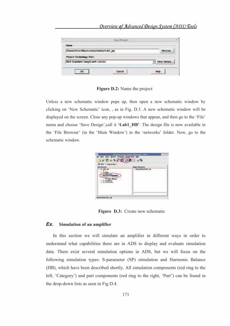
Figure D.2: Name the project
Unless a new schematic window pops up, then open a new schematic window by
clicking on ‘New Schematic’ icon, , as in Fig. D.3. A new schematic window will be
displayed on the screen. Close any pop-up windows that appear, and then go to the ‘File’
menu and choose ‘Save Design’,call it ‘Lab1_HB’. The design file is now available in
the ‘File Browser’ (in the ‘Main Window’) in the ‘networks’ folder. Now, go to the
schematic window.
Figure D.3: Create new schematic
Ex. Simulation of an amplifier
In this section we will simulate an amplifier in different ways in order to
understand what capabilities there are in ADS to display and evaluate simulation
data. There exist several simulation options in ADS, but we will focus on the
following simulation types: S-parameter (SP) simulation and Harmonic Balance
(HB), which have been described shortly. All simulation components (red ring to the
left, ‘Category’) and part components (red ring to the right, ‘Part’) can be found in
the drop-down lists as seen in Fig D.4.

Overview of Advanced Design System (ADS) Tools
172
Figure D.4: "Category" and "Part" drop-down list
D.4 Simulation modes
A brief description of simulation involved in LNA and mixer has been presented
here and details can be found in [D.1]. The main simulation of LNA and mixer are
S-parameters and HB simulation which are given below.
D.4.1 S-parameter (SP) simulation
The S-parameter controller (‘S_Param’) is used to define the signal-wave
response of an n-port electrical element at a given frequency. It is a type of
small-signal AC simulation that is commonly used to characterize a passive RF
component and establish the small-signal characteristics of a device at a specific bias
and temperature. The simulation tasks involving S-parameters also include
information about how to optimize component values and simulation expressions. If
there is not a perfect match between the output port and input port in above mention
block. Therefore, in the S-parameter simulation we need to adjust the input and
output impedances of the amplifier for some mismatch, and then create matching
networks in order to correct this mismatch and achieve good amplification [D.1].

Overview of Advanced Design System (ADS) Tools
173
Then click on the SP control box and enable this control by clicking on the
‘disable’ button. Consequently, the disable button can be used for both disabling and
enabling components, not only control boxes but also e.g. resistors and signal
sources. Add five variables to a ‘Var’ box:
Name Value
Zin 100
Zout 25
fStart 0.1
fStop 1.9
fStep 0.025
Double-click on the amplifier symbol and set parameters and follows:
Name Value
Z1 Zin
Z2 Zout
By setting these impedance parameters it means that the amplifier will relate its
S-parameters to these impedance values. This section also shows how circuit
parameters can be optimized based on user-defined requirements in the S-parameters
control box change as shown in Fig.D.5: the simulated S-parameters data are
obtained as shown in Fig. D.6. In the S-parameter simulation there is no need to
change anything, but the message will disappear if the ‘MeasEqn’ box is disabled. As
before an empty new DDW is displayed on the screen. Click on the plot symbol,
and several new data items are available for representing the data.
(a) (b)
Figure D.5: (a) S-parameters control box (b) Modifications used for simulations.

Overview of Advanced Design System (ADS) Tools
174
Figure D.6: S-parameter simulation data
D.4.2 Harmonic Balance (HB) simulation
The harmonic balance (‘HB’) controller is used for simulating analog/RF and
microwave circuits considered as non-linear. Within the context of high-frequency
circuit and system simulation, harmonic balance offers benefits over conventional
time-domain transient analysis. Harmonic balance captures the steady-state spectral
response directly while conventional transient methods must integrate over many
periods of the lowest-frequency sinusoid to reach steady state. Harmonic balance is
faster at solving typical high-frequency problems that transient analysis can not
accurately solve or can solve at prohibitive costs. It is more accurate at solving high
frequencies where many linear models are best represented in the frequency domain.
Use the HB controller to determine the spectral content of voltages or currents,
calculate quantities such as third-order intercept points, total harmonic distortion,
inter-modulation distortion components and noise.
Initially, we will not run different simulation types at the same time. Therefore,
choosing at first the HB, we would like to disable the ‘S-parameters’ and ‘Envelope’

Overview of Advanced Design System (ADS) Tools
175
simulation boxes which can achieved by selecting the both boxes and clicking on the
symbol, in the menu as shown in Fig.D.7. Now, only the HB simulation mode is
available.
Figure D.7: Disabling simulation control boxes.
To run the simulations, press the simulation button, in the menu. A small
simulation window will pop-up and tell the user about the status of the simulation. If
the simulation is successfully completed, a ‘Data display window’ (DDW) with the
same name as the design will be opened, in this case ‘Lab1_HB’. In ADS there exist
three types of files related to an actual design. They are design file (.dsn): schematic
(and layout) for each design in the networks folder, data display window (.dds): the
window where the simulation results can be displayed. This file is saved in the
project directory. Data set (.ds): the simulation results are saved in the ‘data’ folder in
the project directory and are created/updated when a simulation is completed. The
DDW is initially empty and can be filled with any operation on the simulation data.
To verify that the amplifier gives a gain of 0 dB (1 in linear scale) we simply plot the
harmonic contents of the ‘vload’. In the list of different display options (see Fig. D.8)

Overview of Advanced Design System (ADS) Tools
176
we choose the regular. plot function, . Click on the symbol and place it in the
empty white space.
Figure D.8: ‘Data display window’, DDW
D.4.3 Two-tone HB simulation with variables
A more sensitive way to evaluate the large signal handling capability of a mixer is
to apply two or more signals to the input. These dual or multiple signals (tones) mix
together and form inter-modulation products. Two-tone simulations are used in the
mixer to evaluate the inter-modulation distortion (IMD) generation in the mixer.
All of the following simulation files require such as select the RF center
frequency (RFfreq), LO frequency (LOfreq), and a spacing frequency, Fspacing,
between the two input signals. Thus, the two RF inputs are located at
RFfreq +/- Fspacing/2. Also one need to specify the load impedance, Zload, and in
some cases, source impedance, Zsource and change the source to a P_nTone , set the all
these values as shown in Fig.D.9 [D.2].
Edit the HB controller as shown in Fig.D.10, adding another frequency, Freq[2],
and the values as shown, using the spacing variable / 2. Also, set Order = 4 for both
and set MaxOrder = 8. In this case, the two RF tones are spaced 1 MHz apart.
Simulate and plot the spectrum of Vout in dBm and put a marker on a desire tone.

Overview of Advanced Design System (ADS) Tools
177
Figure D.9: Two-tone HB balance controller input port
Figure D.10: Two-tone HB controller

Overview of Advanced Design System (ADS) Tools
178
References
[D.1] Advanced Design System (ADS) 2012; www.agilent.com.
[D.2] Mixer design guide from ADS manual-2011.