Embed Size (px)
Citation preview
REVIEW
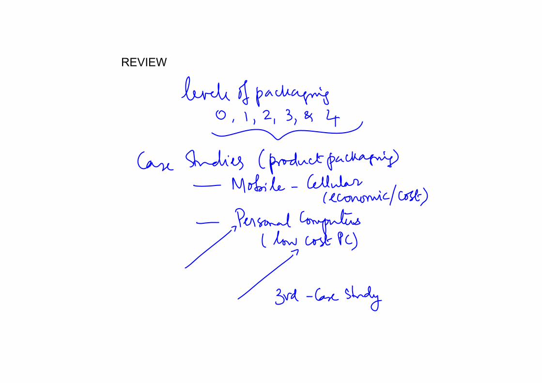
!"#$%&'"!()!$*+,-,./0!"102+3,452!678+0-8!!
&30804+!9!/037!:5;2*1+!,<039.4=!04/53,4-04+!! !!!!',4=!109:!.-08!+,!:0/01,<>!+,,1>!94:!?*915@7!!!!!!!!!A0@,30!<3,:*2.,4!! !!!!B5=C!10/01!,@!+02C45291!94:!<038,4401!8*<<,3+!!! !!!!',D!<3,E+!-93=548!!!$*+,-,./0!"102+3,452!678+0-8!930!F19885E0:!54+,!!! !!!!"4=540!2,4+3,1!94:!-949=0-04+!878+0-8!! !!!!G3948-5885,4!2,4+3,11038!! !!!!F3*580!2,4+3,11038!!
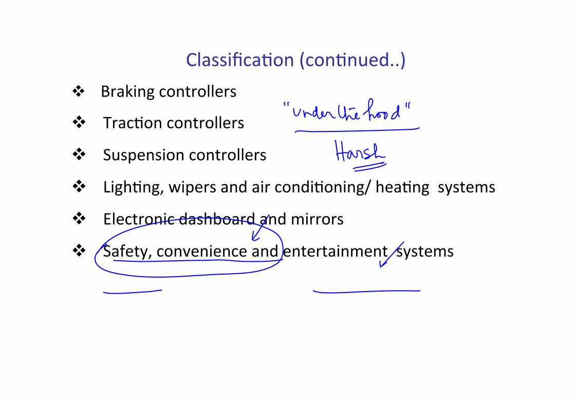
F19885E29.,4!H2,4.4*0:IIJ!! !!!!K39L54=!2,4+3,11038!
! !!!!G392.,4!2,4+3,11038!
! !!!!6*8<0485,4!2,4+3,11038!
! !!!!'5=C.4=>!D5<038!94:!953!2,4:5.,454=M!C09.4=!!878+0-8!!
! !!!!"102+3,452!:98CA,93:!94:!-533,38!!
! !!!!69@0+7>!2,4/0450420!94:!04+03+954-04+!!878+0-8!
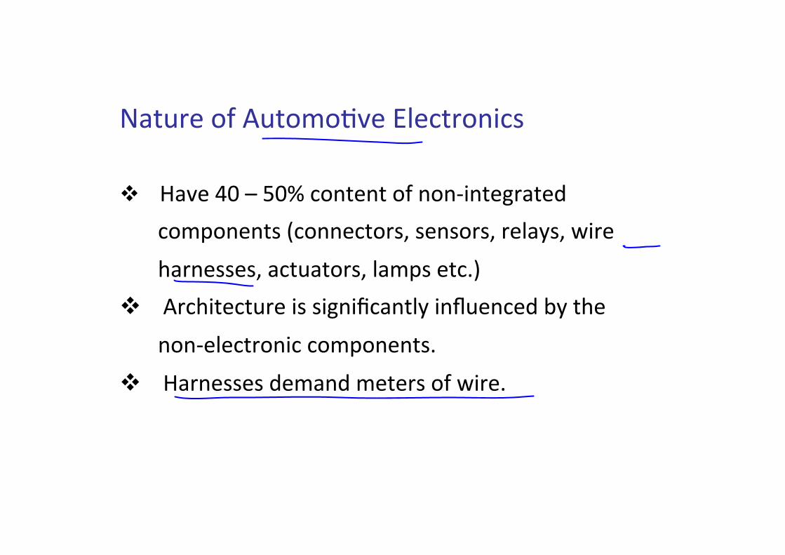
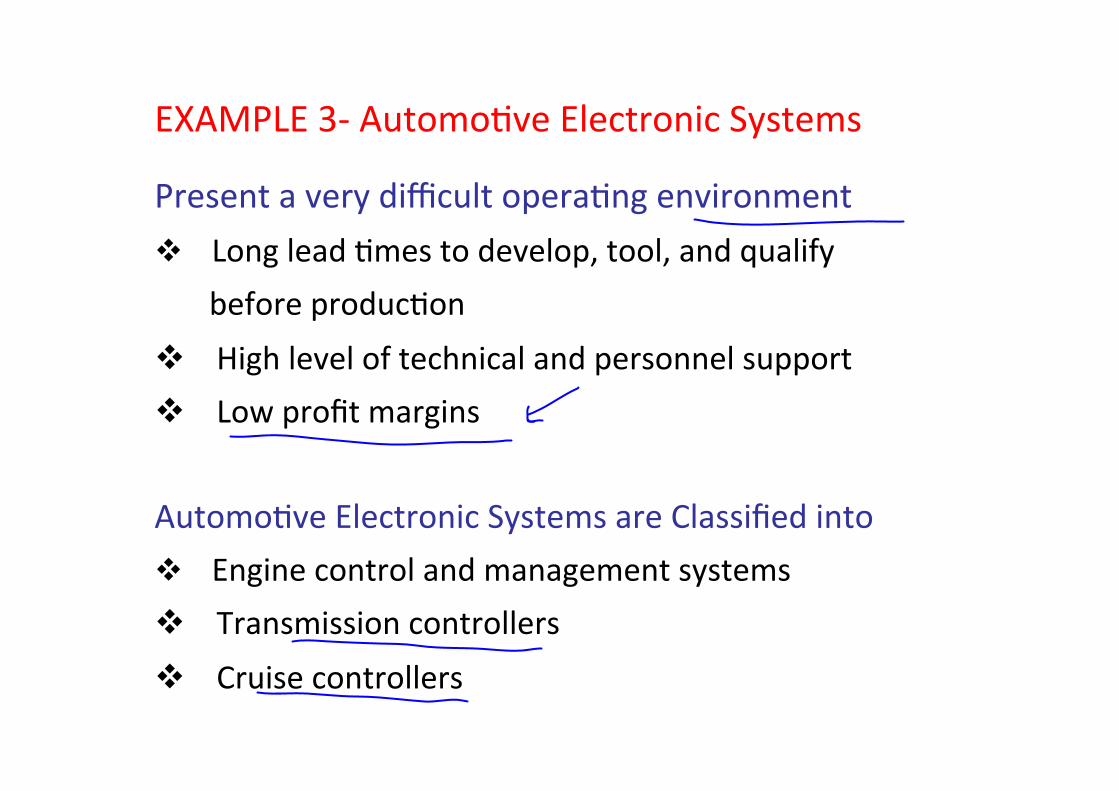
!N9+*30!,@!$*+,-,./0!"102+3,4528!!! !!!!B9/0!OP!Q!RPS!2,4+04+!,@!4,4)54+0=39+0:!!!!!!!!2,-<,404+8!H2,4402+,38>!8048,38>!301978>!D530!!!!!!!!C93408808>!92+*9+,38>!19-<8!0+2IJ!! !!!!$32C5+02+*30!58!85=45E294+17!54T*0420:!A7!+C0!!!!!!!!!4,4)0102+3,452!2,-<,404+8I!! !!!!B93408808!:0-94:!-0+038!,@!D530I!!
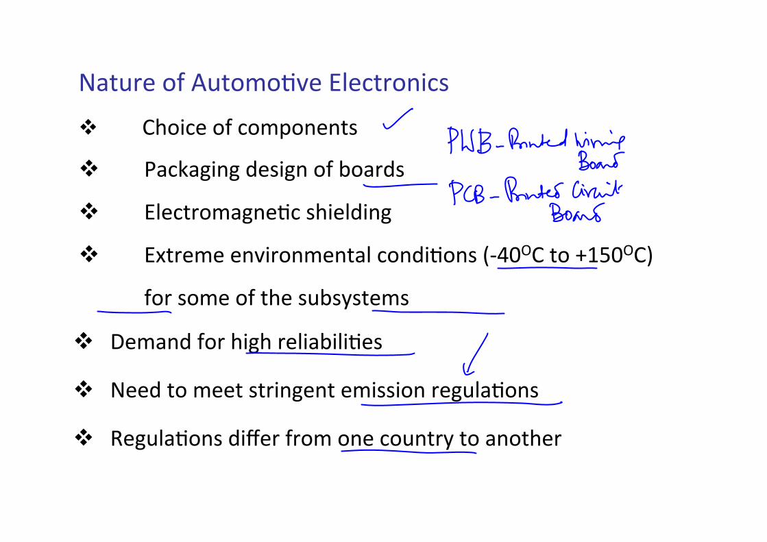
N9+*30!,@!$*+,-,./0!"102+3,4528!
! !FC,520!,@!2,-<,404+8!
! ! !&92L9=54=!:085=4!,@!A,93:8!
! ! !"102+3,-9=40.2!8C501:54=!
! ! !"U+30-0!04/53,4-04+91!2,4:5.,48!H)OPVF!+,!WXRPVFJ!
!@,3!8,-0!,@!+C0!8*A878+0-8!!!! !!!Y0-94:!@,3!C5=C!30159A515.08!
! !!!N00:!+,!-00+!8+354=04+!0-5885,4!30=*19.,48!
! !!!Z0=*19.,48!:5[03!@3,-!,40!2,*4+37!+,!94,+C03!!
F,421*85,4!FC9<+03!X!\!F*3304+!+304:8!54!&92L9=54=!!!!!!!!!!!!!!!60-52,4:*2+,38!!
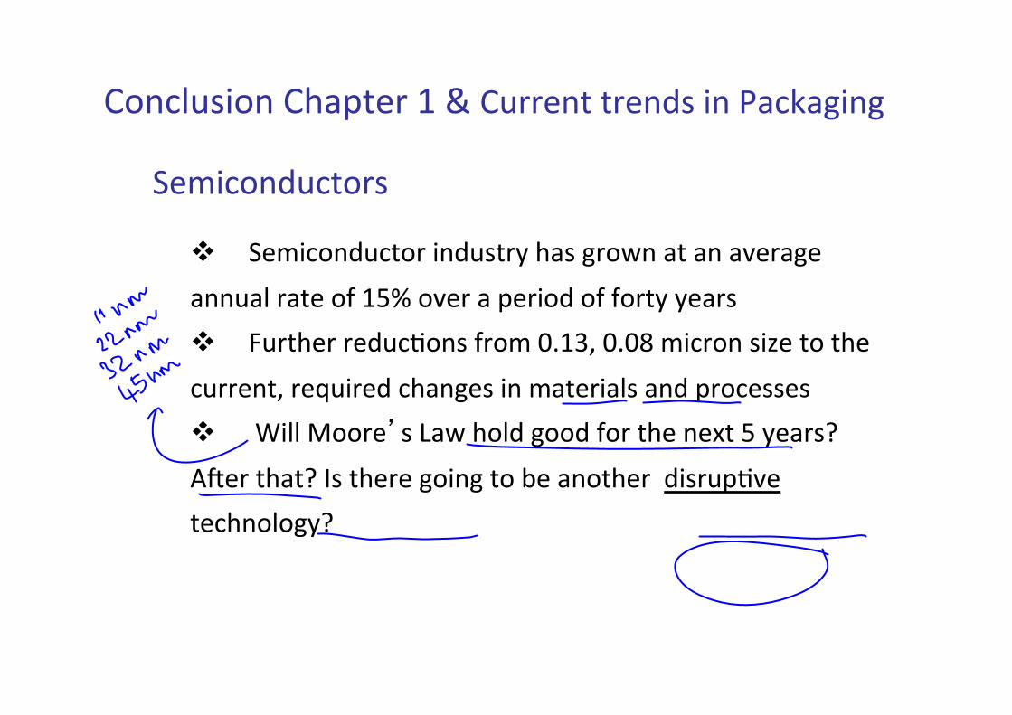
! !!!!!60-52,4:*2+,3!54:*8+37!C98!=3,D4!9+!94!9/039=0!944*91!39+0!,@!XRS!,/03!9!<035,:!,@!@,3+7!70938!! !!!!!]*3+C03!30:*2.,48!@3,-!PIX(>!PIP^!-523,4!85_0!+,!+C0!2*3304+>!30?*530:!2C94=08!54!-9+035918!94:!<3,208808!! !!!!!!`511!%,,30’8!'9D!C,1:!=,,:!@,3!+C0!40U+!R!70938a!$b03!+C9+a!c8!+C030!=,54=!+,!A0!94,+C03!!:583*<./0!+02C4,1,=7a!
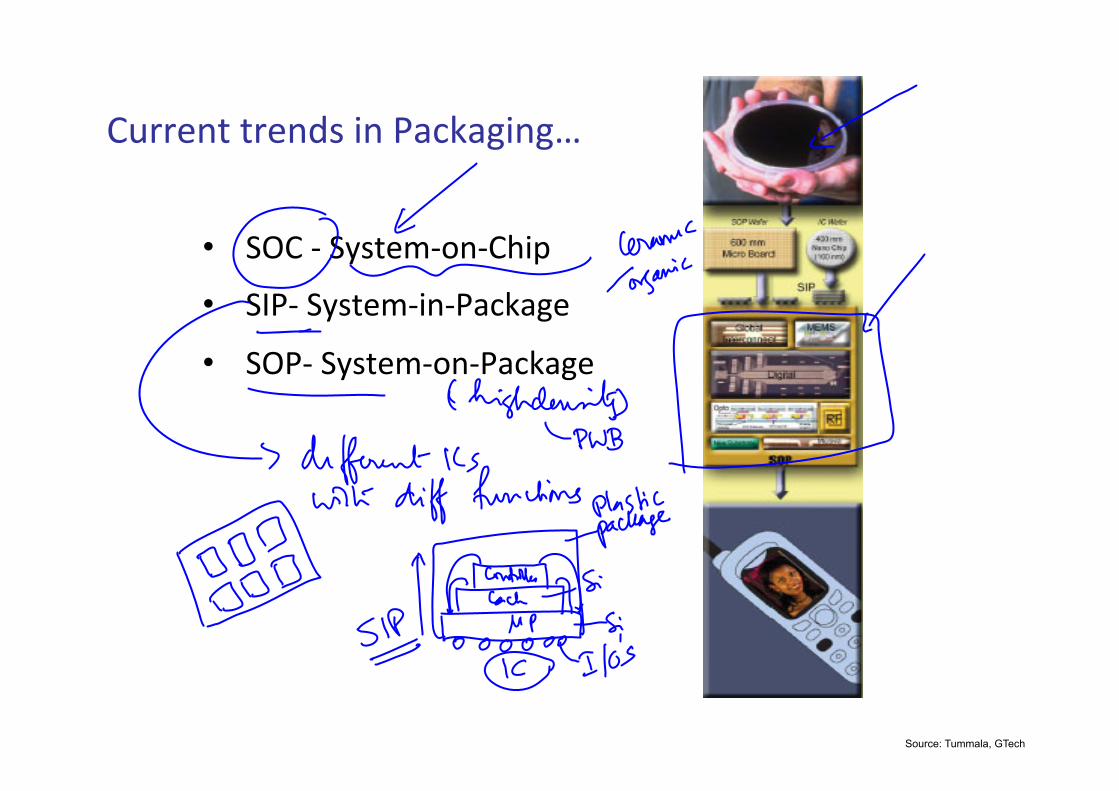
F*3304+!+304:8!54!&92L9=54=d!!
• !!!!6VF!)!678+0-),4)FC5<!
• !!!!6c&)!678+0-)54)&92L9=0 !!!
• !!!!6V&)!678+0-),4)&92L9=0!
Source: Tummala, GTech
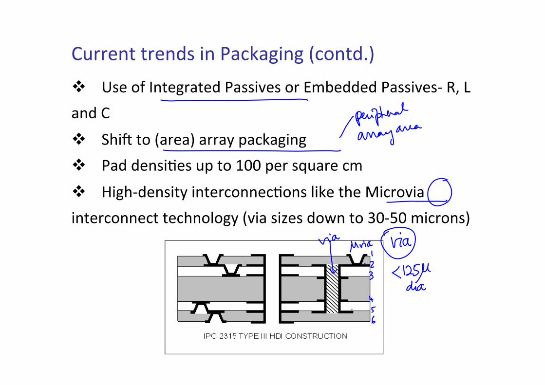
F*3304+!+304:8!54!&92L9=54=!H2,4+:IJ!!
! !!!!e80!,@!c4+0=39+0:!&9885/08!,3!"-A0::0:!&9885/08)!Z>!'!94:!F!! !!!!6C5b!+,!H9309J!93397!<92L9=54=!! !!!!&9:!:0485.08!*<!+,!XPP!<03!8?*930!2-!! !!!!B5=C):0485+7!54+032,4402.,48!15L0!+C0!%523,/59!54+032,4402+!+02C4,1,=7!H/59!85_08!:,D4!+,!(P)RP!-523,48J!
&354+0:!`5354=!K,93:!H&`KJ!!! !!!!GC0!-,8+!5-<,3+94+!,@!878+0-!10/01!<92L9=08!
! !!!!&3,/5:08!54+032,4402.,48!9-,4=!:0/5208!+C3,*=C!!
!!!!!!!5+8!!2,<<03!+392L8!!
! !!!!%02C945291!8*<<,3+!+,!+C0!2,-<,404+8!!
&354+0:!`5354=!K,93:!H&`KJd!
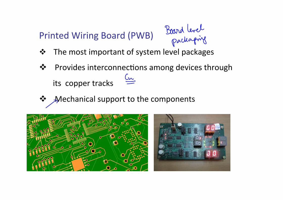
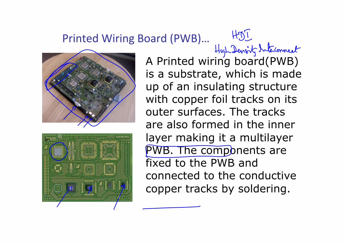
A Printed wiring board(PWB) is a substrate, which is made up of an insulating structure with copper foil tracks on its outer surfaces. The tracks are also formed in the inner layer making it a multilayer PWB. The components are fixed to the PWB and connected to the conductive copper tracks by soldering.
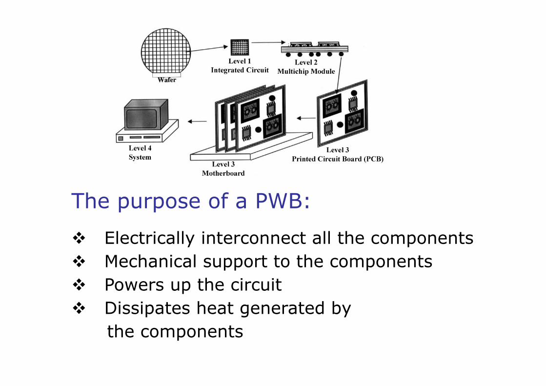
The purpose of a PWB:
! Electrically interconnect all the components ! Mechanical support to the components ! Powers up the circuit ! Dissipates heat generated by the components
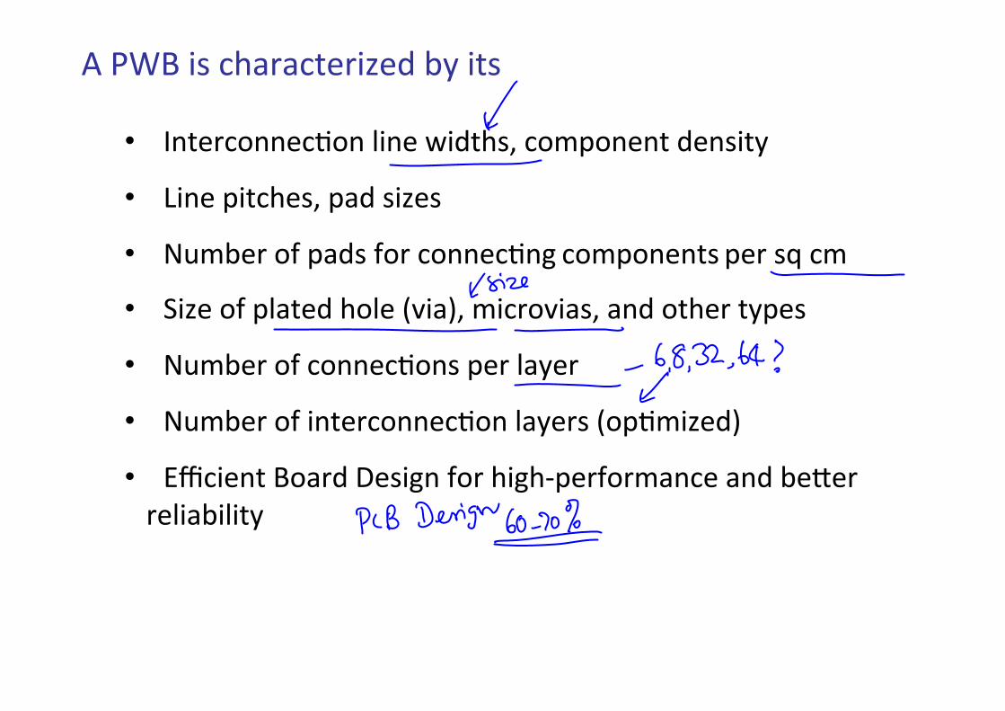
$!&`K!58!2C9392+035_0:!A7!5+8!!!
• !!!!c4+032,4402.,4!1540!D5:+C8>!2,-<,404+!:0485+7!
• !!!!'540!<5+2C08>!<9:!85_08!
• !!!!N*-A03!,@!<9:8!@,3!2,4402.4=!2,-<,404+8!<03!8?!2-!
• !!!!65_0!,@!<19+0:!C,10!H/59J>!-523,/598>!94:!,+C03!+7<08!
• !!!!N*-A03!,@!2,4402.,48!<03!19703!
• !!!!N*-A03!,@!54+032,4402.,4!197038!H,<.-5_0:J!
• !!!!";2504+!K,93:!Y085=4!@,3!C5=C)<03@,3-9420!94:!A0f03!!!!!!30159A515+7!
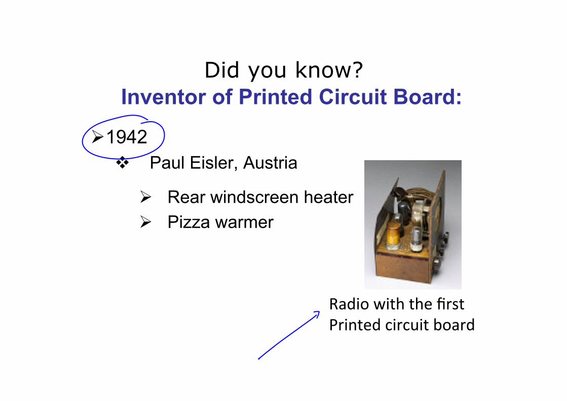
Did you know? Inventor of Printed Circuit Board:
" 1942 ! Paul Eisler, Austria
" Rear windscreen heater " Pizza warmer
Z9:5,!D5+C!+C0!E38+!&354+0:!2532*5+!A,93:!
Next Chapter is on “Semiconductor packaging” “Semiconductor process overview”
Chapter 1 ends here and it’s time for tutorials
TUTORIALS
Please do further reading on the chapter by using the suggested textbooks- details given in introduction class.
Q-1 What is a microsystem? Compare with microelectronics. A microsystem is a microminiaturized and integrated system based on microelectronics, RF, photonics, micro-electro-mechanical systems, and packaging technologies. A microsystem provides a number of integrated functions such as computing, communication, consumer and sensing to serve a variety of human needs. In contrast, microelectronics is based on three circuit elements; transistors, capacitors and resistors, fabricated at sub micron dimensions as an “integrated circuit” or IC. The IC forms the basis for most of today’s microelectronic systems of which computers are an example.
Q-2 Why integrate microsystem technologies into single products? Microsystem technologies which includes digital, RF, optical, MEMS and sensing technologies are integrated into single miniaturized products in order to provide services and functions in the least amount of space and at least cost. A cell phone is an example of a microsystem. It is a microminiaturized, integrated system—a computer and a wireless product, based on processors, RF passives, MEMs switches, display technology, image acquisition and human interface technology via voice or key pad. It is compact and convenient to use and is cheap to manufacture because of high volume fabrication.
Q-3 What is the role of packaging in microsystems? Packaging provides a set of interconnections at IC or device level as well as at the interface and interconnections between ICs, MEMS, photonic, RF, and other components into a System- level board to form electronic products. Historically, these interconnections have been electrical. As microsystem performance increases, we may see photonic interconnections in the near future.
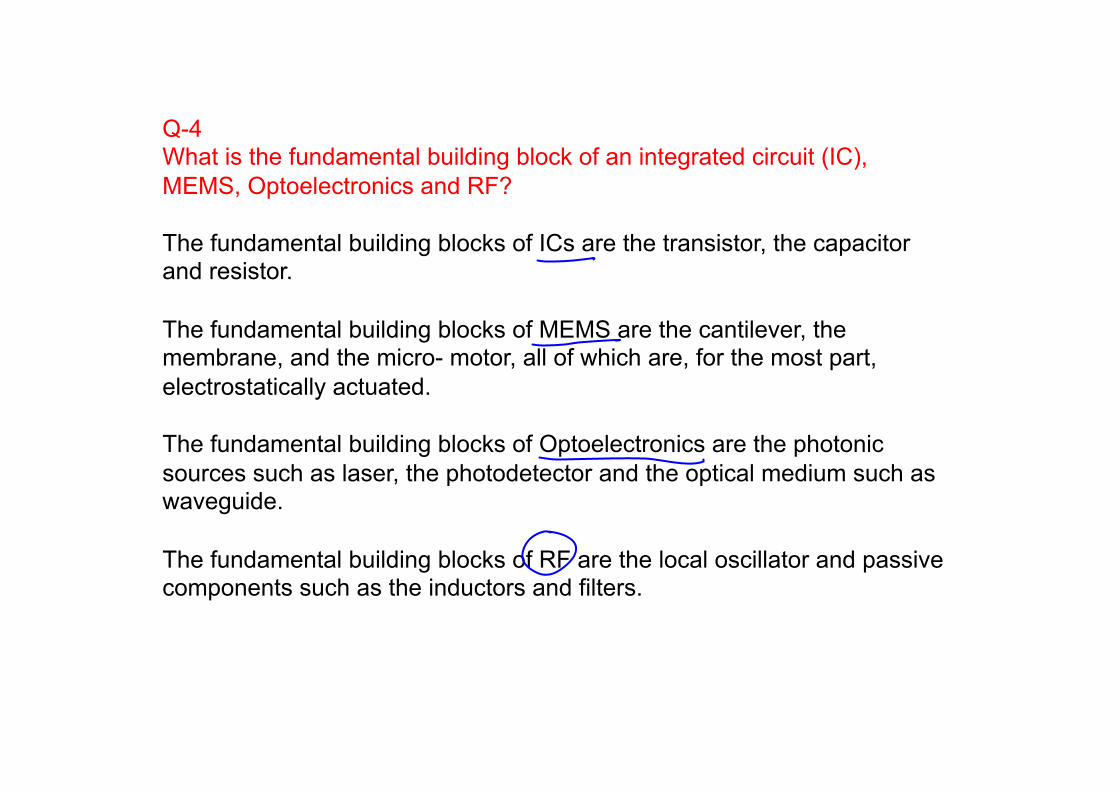
Q-4 What is the fundamental building block of an integrated circuit (IC), MEMS, Optoelectronics and RF? The fundamental building blocks of ICs are the transistor, the capacitor and resistor. The fundamental building blocks of MEMS are the cantilever, the membrane, and the micro- motor, all of which are, for the most part, electrostatically actuated. The fundamental building blocks of Optoelectronics are the photonic sources such as laser, the photodetector and the optical medium such as waveguide. The fundamental building blocks of RF are the local oscillator and passive components such as the inductors and filters.
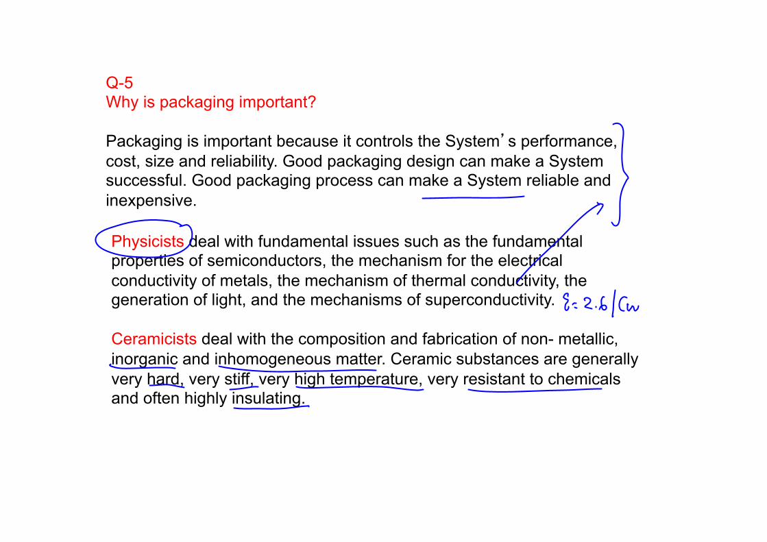
Q-5 Why is packaging important? Packaging is important because it controls the System’s performance, cost, size and reliability. Good packaging design can make a System successful. Good packaging process can make a System reliable and inexpensive.
Physicists deal with fundamental issues such as the fundamental properties of semiconductors, the mechanism for the electrical conductivity of metals, the mechanism of thermal conductivity, the generation of light, and the mechanisms of superconductivity. Ceramicists deal with the composition and fabrication of non- metallic, inorganic and inhomogeneous matter. Ceramic substances are generally very hard, very stiff, very high temperature, very resistant to chemicals and often highly insulating.
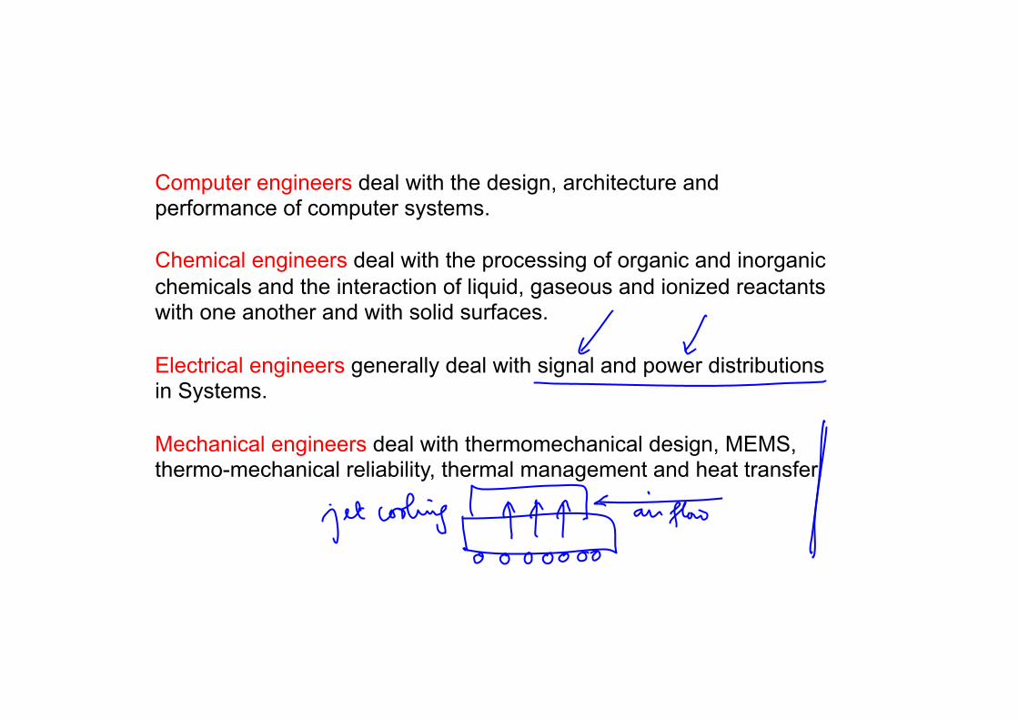
Computer engineers deal with the design, architecture and performance of computer systems. Chemical engineers deal with the processing of organic and inorganic chemicals and the interaction of liquid, gaseous and ionized reactants with one another and with solid surfaces. Electrical engineers generally deal with signal and power distributions in Systems. Mechanical engineers deal with thermomechanical design, MEMS, thermo-mechanical reliability, thermal management and heat transfer.
Q-6 Why are packaging considerations for automotive electronics different? The main factor that distinguishes automotive electronics products from consumer electronics products is the environment in which they must perform. Cost, size and weight reductions are also major factors that influence packaging of automotive electronics products. Automotive control systems packaging requirements are not similar to conventional printed circuit-board mounted plastic or ceramic units. Processing is distributed around the vehicle as dictated by the locations of sensors and actuators, and packaging requirements are changing accordingly.
Tutorial references taken from “Fundamentals of Microelectronics Sys Packaging” Rao Tummala
To the next TOPIC now..
Next Chapter is on “Semiconductor packaging” “Semiconductor process overview”