Embed Size (px)
Citation preview
Review for Midterm #2
Wireless Networking and Communications Group
April 19, 2023
Prof. Brian L. Evans
EE 445S Real-Time Digital Signal Processing Laboratory
2
Outline
Introduction Signal processing building blocks
Filters Data conversion Rate changers
Communication systems
Design tradeoffs in signal quality vs. implementation complexity
3
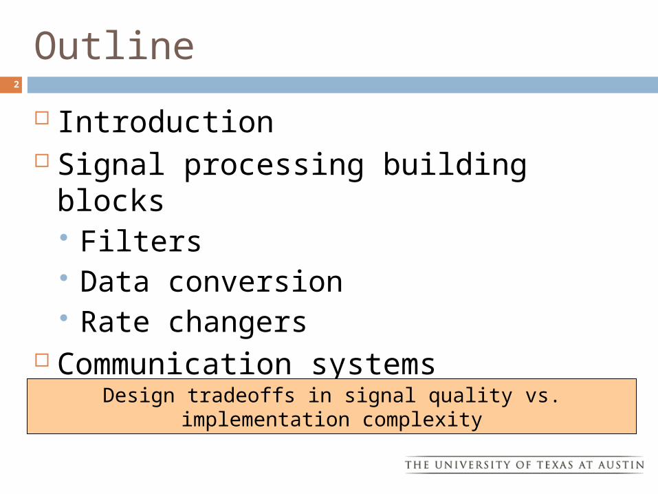
Introduction Signal processing algorithms
Multirate processing: e.g. interpolation Local feedback: e.g. IIR filters Iteration: e.g. phase locked loops
Signal representations Bits, symbols Real-valued symbol amplitudes Complex-valued symbol amplitudes (I-Q) Vectors/matrices of scalar data types
Algorithm implementation Dominated by multiplication/addition High-throughput input/output
Do not needrecursion
Often iterative
Bit error rate vs. Signal-to-noise ratio (Eb/No)
Communication signal quality plot
4
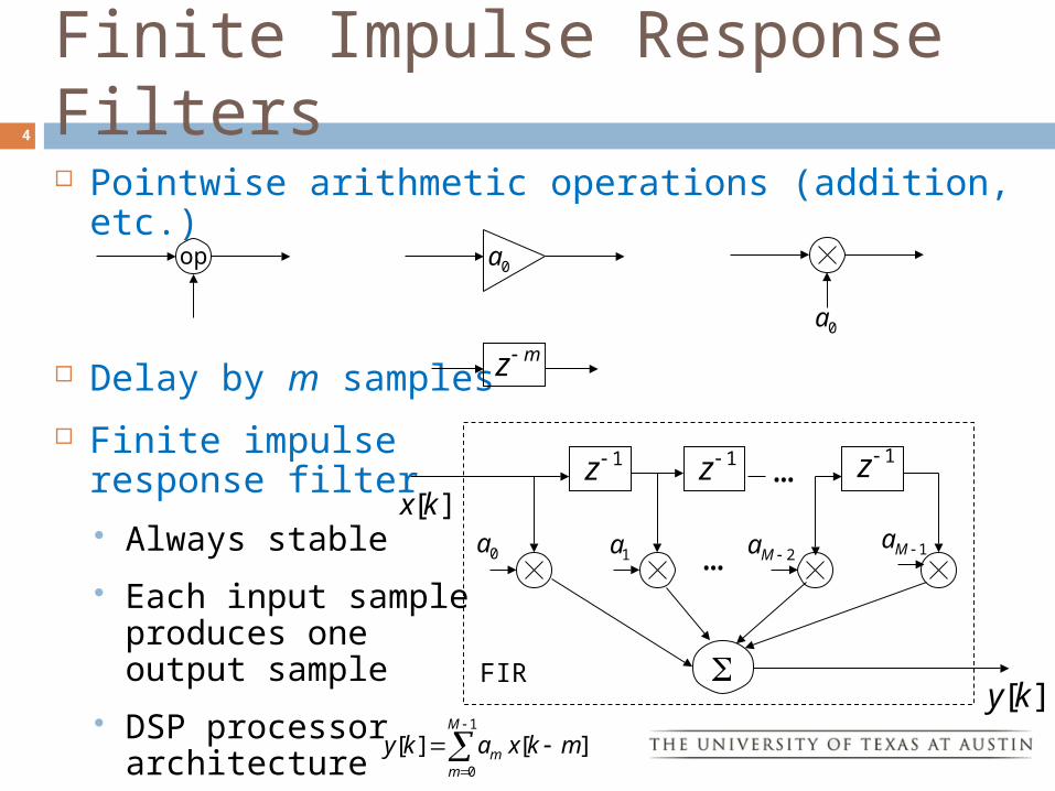
Finite Impulse Response Filters Pointwise arithmetic operations (addition, etc.)
Delay by m samples Finite impulse
response filter Always stable Each input sample
produces oneoutput sample
DSP processorarchitecture
0a
op
0amz
1
0
][ ][M
mm mkxaky
][kx
1z
][ky
0a 1Ma2Ma1a …
…1z1z
FIR
5
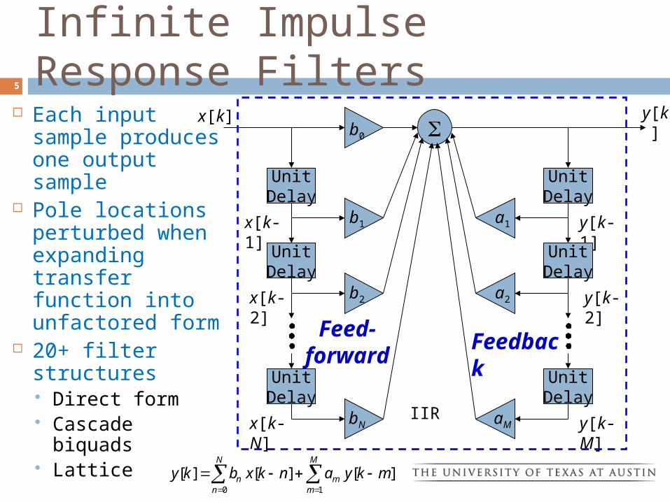
Infinite Impulse Response Filters
M
mm
N
nn mkyankxbky
10
][ ][ ][
x[k] y[k]
y[k-M]
x[k-1]
x[k-2] b2
b1
b0
UnitDelay
UnitDelay
UnitDelay
x[k-N] bN
Feed-forward
a1
a2
y[k-1]
y[k-2]
UnitDelay
UnitDelay
UnitDelay
aM
Feedback
IIR
Each inputsample producesone output sample
Pole locations perturbed when expanding transfer function into unfactored form
20+ filter structures Direct form Cascade biquads Lattice
6
Data Conversion
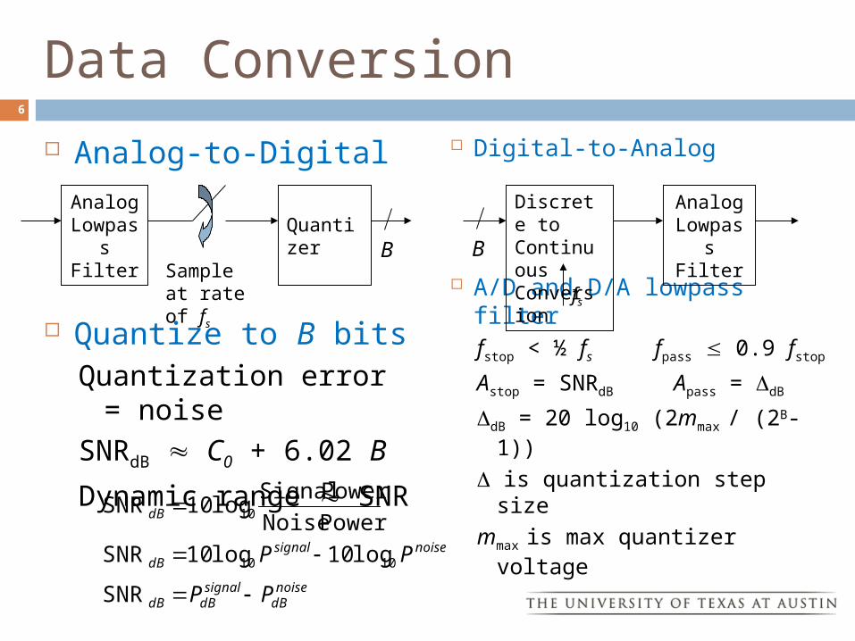
Analog-to-Digital
Quantize to B bitsQuantization error = noiseSNRdB C0 + 6.02 B
Dynamic range SNR
Digital-to-Analog
A/D and D/A lowpass filterfstop < ½ fs fpass 0.9 fstop
Astop = SNRdB Apass = dB
dB = 20 log10 (2mmax / (2B-1))
is quantization step sizemmax is max quantizer voltage
Analog Lowpass
Filter
Discrete to Continuous Conversion
fs
Analog Lowpass
FilterQuantizer
Sample at rate of fs
noisedB
signaldBdB
noisesignaldB
dB
PP
PP
SNR
log10log10SNR
Power Noise
Power Signallog10SNR
1010
10
B B
7
7
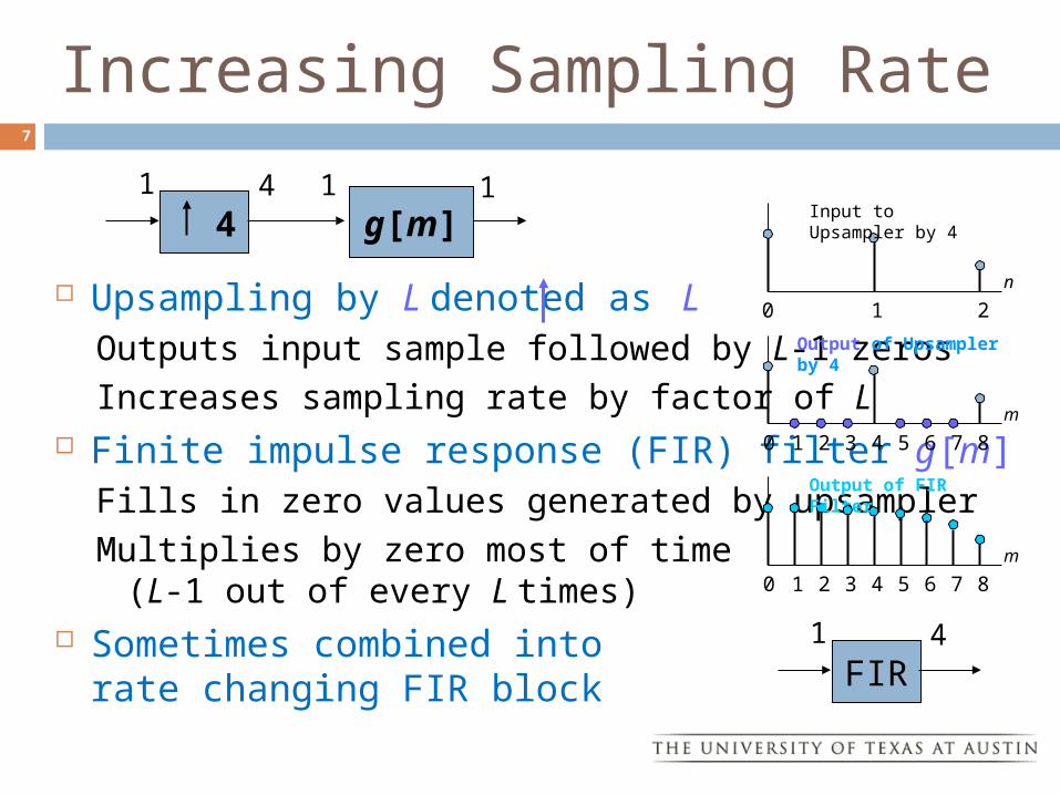
Increasing Sampling Rate
Upsampling by L denoted as LOutputs input sample followed by L-1 zerosIncreases sampling rate by factor of L
Finite impulse response (FIR) filter g[m]Fills in zero values generated by upsamplerMultiplies by zero most of time
(L-1 out of every L times) Sometimes combined into
rate changing FIR block
m
Output of Upsampler by 4
1 2 3 4 5 6 7 80
1 2
Output of FIR Filter
3 4 5 6 7 8
m
0
1 2
Input to Upsampler by 4
n
0
g[m] 41 4 1 1
FIR1 4
8
8
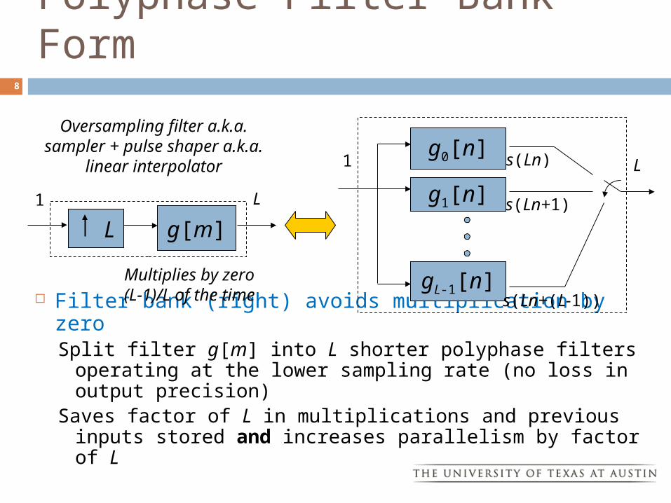
Polyphase Filter Bank Form
Filter bank (right) avoids multiplication by zeroSplit filter g[m] into L shorter polyphase filters operating at the
lower sampling rate (no loss in output precision)Saves factor of L in multiplications and previous inputs stored and increases parallelism by factor of L
g0[n]
g1[n]
gL-1[n]
s(Ln)
s(Ln+1)
s(Ln+(L-1))
g[m] L
Oversampling filter a.k.a. sampler + pulse shaper a.k.a.
linear interpolator
Multiplies by zero (L-1)/L of the time
1 L
L1
9
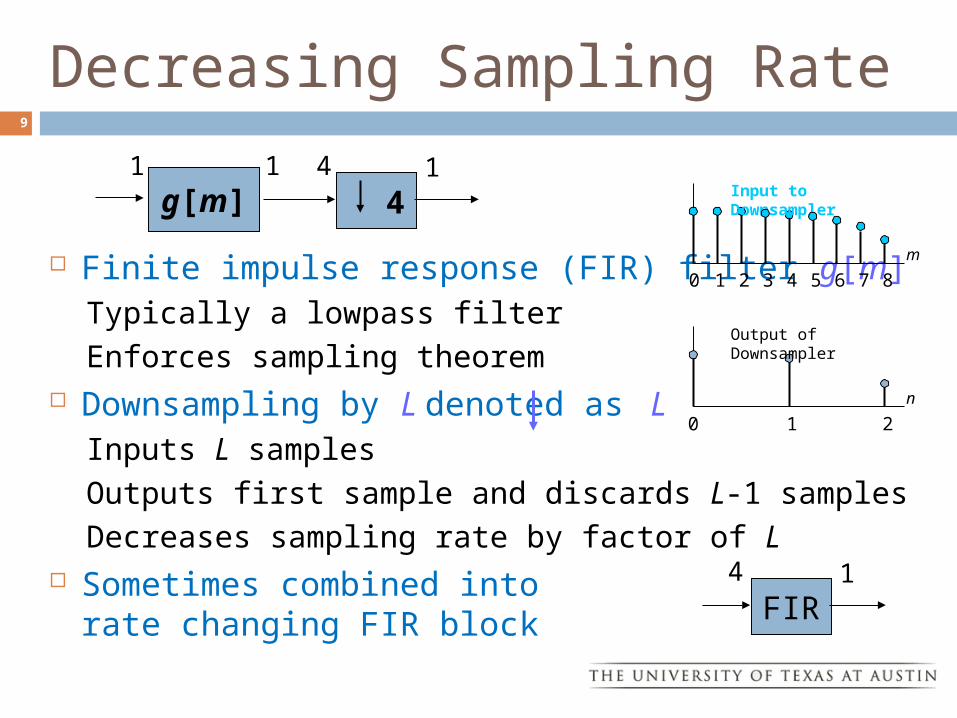
Decreasing Sampling Rate
Finite impulse response (FIR) filter g[m]Typically a lowpass filterEnforces sampling theorem
Downsampling by L denoted as LInputs L samplesOutputs first sample and discards L-1 samplesDecreases sampling rate by factor of L
Sometimes combined intorate changing FIR block
44 1
g[m]1 1
1 2
Input to Downsampler
3 4 5 6 7 8
m
0
1 2
Output of Downsampler
n
0
FIR4 1
10
10
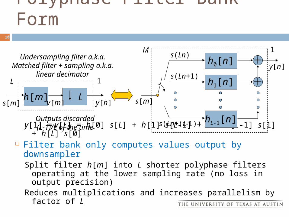
Polyphase Filter Bank Form
y[1] = v[L] = h[0] s[L] + h[1] s[L-1] + … + h[L-1] s[1] + h[L] s[0] Filter bank only computes values output by downsampler
Split filter h[m] into L shorter polyphase filters operating at the lower sampling rate (no loss in output precision)
Reduces multiplications and increases parallelism by factor of L
h0[n]
h1[n]
hL-1[n]
h[m] L
s(Ln)
s(Ln+1)
s(Ln+(L-1))
Undersampling filter a.k.a. Matched filter + sampling a.k.a.
linear decimator
Outputs discarded (L-1)/L of the time
1
1
L
M
s[m] s[m]y[n]
y[n]
v[m]
11
11
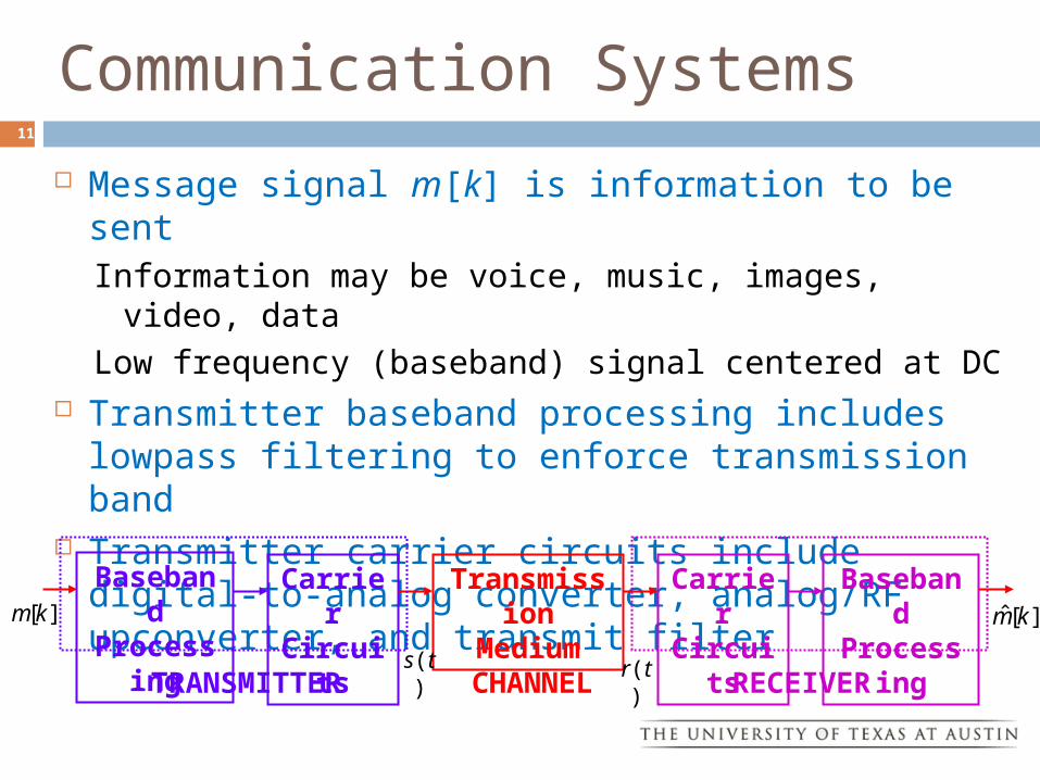
Communication Systems
Message signal m[k] is information to be sentInformation may be voice, music, images, video, dataLow frequency (baseband) signal centered at DC
Transmitter baseband processing includes lowpass filtering to enforce transmission band
Transmitter carrier circuits include digital-to-analog converter, analog/RF upconverter, and transmit filter
BasebandProcessing
CarrierCircuits
Transmission Medium
Carrier Circuits
BasebandProcessing
TRANSMITTER RECEIVERs(t) r(t)
][ˆ km
CHANNEL
][km
12
12
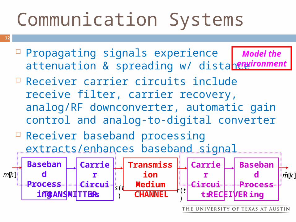
Communication Systems
Propagating signals experienceattenuation & spreading w/ distance
Receiver carrier circuits include receive filter, carrier recovery, analog/RF downconverter, automatic gain control and analog-to-digital converter
Receiver baseband processing extracts/enhances baseband signal
BasebandProcessing
CarrierCircuits
Transmission Medium
Carrier Circuits
BasebandProcessing
TRANSMITTER RECEIVERs(t) r(t)
][ˆ km
CHANNEL
][km
Model the environment
13
13
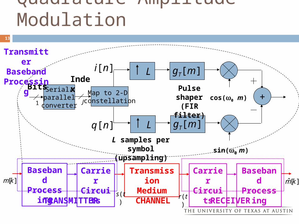
Quadrature Amplitude Modulation
i[n] gT[m] L
+cos(0 m)
q[n] gT[m] L
sin(0 m)
Serial/parallel
converter1
BitsMap to 2-D constellationJ
L samples per symbol (upsampling)
Transmitter Baseband Processing
Pulse shaper
(FIR filter)
Index
BasebandProcessing
CarrierCircuits
Transmission Medium
Carrier Circuits
BasebandProcessing
TRANSMITTER RECEIVERs(t) r(t)
][ˆ km
CHANNEL
][km
14
14
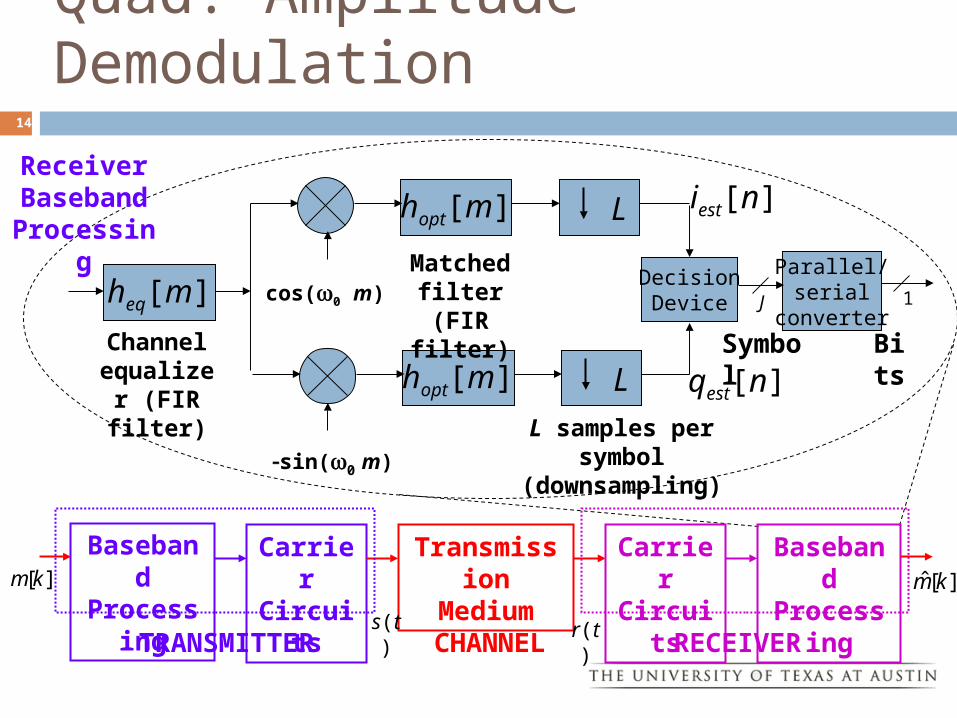
Quad. Amplitude Demodulation
iest[n]hopt[m] L
cos(0 m)
hopt[m] L
sin(0 m)
L samples per symbol (downsampling)
Matched filter
(FIR filter)
qest[n]
Parallel/serial
converterJ
Bits
DecisionDevice 1
Symbol
BasebandProcessing
CarrierCircuits
Transmission Medium
Carrier Circuits
BasebandProcessing
TRANSMITTER RECEIVERs(t) r(t)
][ˆ km
CHANNEL
][km
heq[m]
Channel equalizer (FIR filter)
Receiver Baseband Processing
15
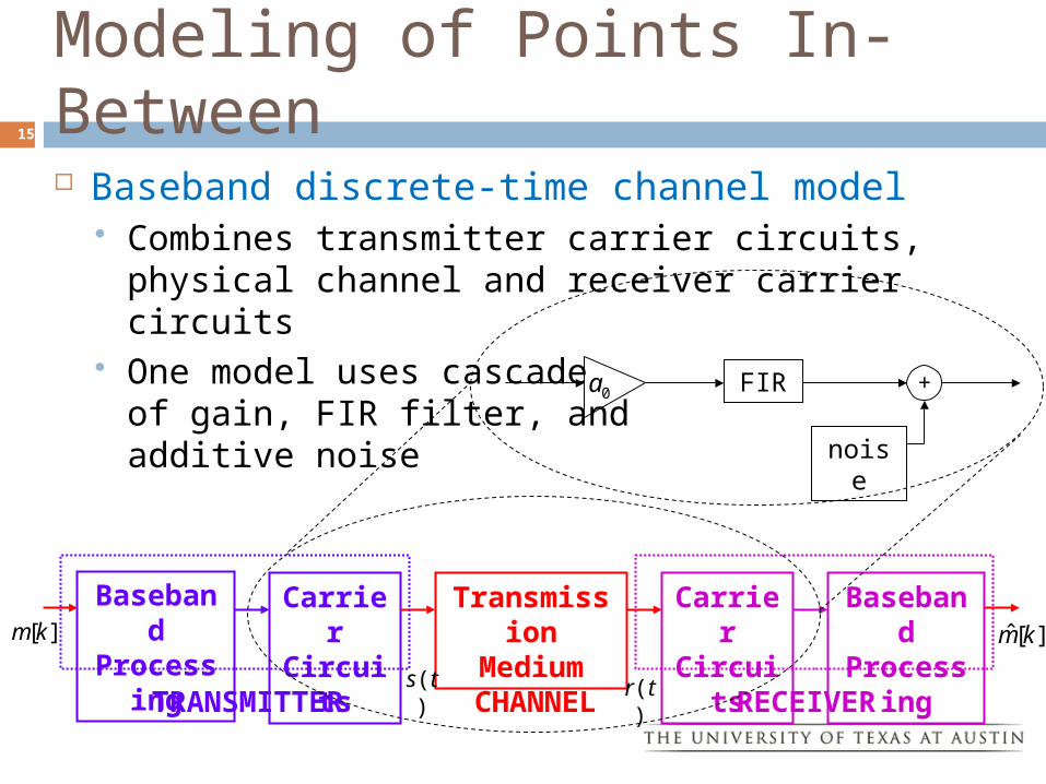
Modeling of Points In-Between
Baseband discrete-time channel model Combines transmitter carrier circuits, physical channel and
receiver carrier circuits One model uses cascade
of gain, FIR filter, andadditive noise
BasebandProcessing
CarrierCircuits
Transmission Medium
Carrier Circuits
BasebandProcessing
TRANSMITTER RECEIVERs(t) r(t)
][ˆ km
CHANNEL
][km
0a FIR +
noise
16
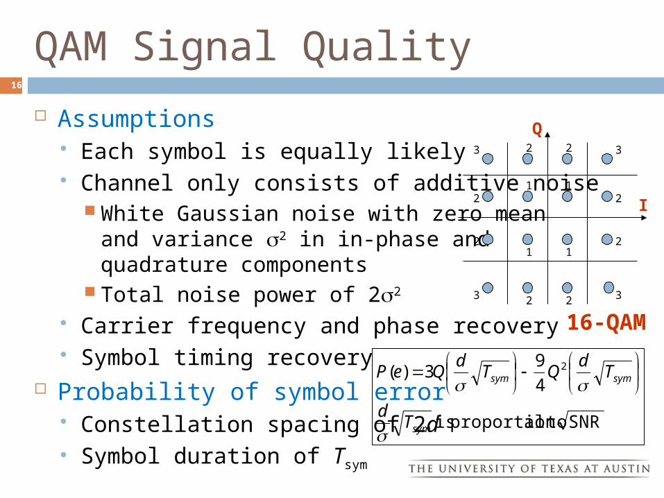
QAM Signal Quality
Assumptions Each symbol is equally likely Channel only consists of additive noise
White Gaussian noise with zero meanand variance 2 in in-phase andquadrature components
Total noise power of 22 Carrier frequency and phase recovery Symbol timing recovery
Probability of symbol error Constellation spacing of 2d Symbol duration of Tsym
3
3
3
3
2 2
2
2
2 2
2
211
1 1
I
Q
16-QAM
SNR toalproportion is
4
93)( 2
sym
symsym
Td
Td
QTd
QeP