Embed Size (px)
Citation preview
1
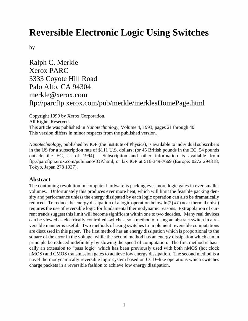
Reversible Electronic Logic Using Switchesby
Ralph C. MerkleXerox PARC3333 Coyote Hill RoadPalo Alto, CA [email protected]://parcftp.xerox.com/pub/merkle/merklesHomePage.html
Copyright 1990 by Xerox Corporation.All Rights Reserved.This article was published in Nanotechnology, Volume 4, 1993, pages 21 through 40.This version differs in minor respects from the published version.
Nanotechnology, published by IOP (the Institute of Physics), is available to individual subscribersin the US for a subscription rate of $111 U.S. dollars; (or 45 British pounds in the EC, 54 poundsoutside the EC, as of 1994). Subscription and other information is available fromftp://parcftp.xerox.com/pub/nano/IOP.html, or fax IOP at 516-349-7669 (Europe: 0272 294318;Tokyo, Japan 278 1937).
AbstractThe continuing revolution in computer hardware is packing ever more logic gates in ever smallervolumes. Unfortunately this produces ever more heat, which will limit the feasible packing den-sity and performance unless the energy dissipated by each logic operation can also be dramaticallyreduced. To reduce the energy dissipation of a logic operation below ln(2) kT (near thermal noise)requires the use of reversible logic for fundamental thermodynamic reasons. Extrapolation of cur-rent trends suggest this limit will become significant within one to two decades. Many real devicescan be viewed as electrically controlled switches, so a method of using an abstract switch in a re-versible manner is useful. Two methods of using switches to implement reversible computationsare discussed in this paper. The first method has an energy dissipation which is proportional to thesquare of the error in the voltage, while the second method has an energy dissipation which can inprinciple be reduced indefinitely by slowing the speed of computation. The first method is basi-cally an extension to “pass logic” which has been previously used with both nMOS (hot clocknMOS) and CMOS transmission gates to achieve low energy dissipation. The second method is anovel thermodynamically reversible logic system based on CCD−like operations which switchescharge packets in a reversible fashion to achieve low energy dissipation.
2
Introduction
There is now a fairly extensive literature on reversible computation[11] which shows that the en-ergy dissipation per device operation cannot be reduced below ln(2) kT (where k is Boltzman’sconstant and T is the temperature; kT is roughly the thermal energy of a single atom) if the deviceis not reversible.
For the last 50 years the energy dissipation per gate operation has been declining with remarkableregularity[6]. Extrapolation of this trend shows the energy dissipation per device operation reach-ing kT by the year 2015. (This assumes that T is 300 Kelvin − more on this later). To gain someperspective on this consider that an “AND” gate which has a power supply of one volt and whichallows 100 electrons to go from that one volt supply to ground during the course of a switchingoperation will dissipate 100 electron volts. Although 100 electron volts is about 4,000 times kT(and well above the theoretical limit), it will be difficult for simple improvements of irreversibleapproaches to reach even this level of energy dissipation. Extrapolating present trends, we shouldreach 4,000 kT before the year 2000, e.g., within ten years. While reversible logic is an absolutenecessity if we are to reduce energy dissipation per device operation below kT, it is a useful heu-ristic for designing systems that have low energy dissipation even when the actual energy dissipa-tion is well above kT.
Even if we do develop irreversible devices that approach ln(2) kT, a computer operating at roomtemperature at a frequency of one gigahertz with 1018 logic gates packed into a volume not muchlarger than a cubic centimeter would dissipate over three megawatts. The drive for ever greatercomputational power with ever more densely packed logic elements will eventually require that asingle logic operation dissipate orders of magnitude energy less than kT. If we are to realize thefull potential of nanoelectronics and molecular logic devices, at some point in the future we willbe forced to use thermodynamically reversible logic elements for a substantial fraction of logic op-erations.
We can state quite confidently that one of three things will occur: (a) the historic rate of decreasingenergy dissipation per device operation will slow or halt in the next one or two decades or (b) wewill operate computers at lower temperatures or (c) we will develop new methods of computing ina reversible way that can beat the kT barrier.
The first option is unattractive. First, cooling is a major problem. The heroic cooling methods usedin the Cray 3 supercomputer to remove the heat generated by the computer’s operation suggest thatfailure to reduce energy dissipation per gate operation would be a major limiting factor in futurecomputer performance. While both air-cooling a single chip that dissipates 150 watts[62] and wa-ter cooling of a chip dissipating 790 watts/cm2 have been demonstrated[64], and more effectivecooling methods should be feasible in the future[18], we will eventually reach a limit to heat re-moval. Second, in many applications power is limited. Portable computers, remote sensors andother isolated systems have only a limited amount of power available. Third, although the raw costof electrical power is not yet a major limitation it would become so in the future if reductions inenergy dissipation did not keep pace with advances in other areas. The Wall Street Journal[63]said “Computer systems currently account for 5% of commercial electricity use in the U.S., withthe potential to grow to 10% by the year 2000.”

3
Operating computers at a lower temperature will not reduce overall energy dissipation. If we op-erated future devices at 3 Kelvins we would reduce kT by a factor of 100 and so could reduce en-ergy dissipation per logic operation by a similar factor − but for fundamental thermodynamic rea-sons the coefficient of performance of the refrigerator for the system can be at best 3K/(300K −3K) ≈ 0.01[5]. Thus, the lower energy required per gate operation will be almost exactly balancedby the increased energy needed by the refrigerator. In many applications refrigeration is not anattractive option. Lap top and portable computers[59], embedded systems, various “smart” appli-ances and other applications make the use of refrigeration undesirable.
Factors other than net energy savings can make low temperature operation worthwhile. For ex-ample, some potentially attractive devices don’t operate at higher temperatures. In large computersoperating in stable environments (the traditional computer center, for example) refrigeration mightbe attractive, particularly if it permits the use of devices that provide much better performance butwhich require low temperature for their operation (Josephson junction devices might be an exam-ple). Refrigeration per se, however, does not seem too attractive.
Finally, and most attractively, we could use reversible computation to reduce energy dissipation.This would, in principle, allow energy dissipations indefinitely below kT per logic operation.While some barrier should eventually be encountered, the use of reversible logic should allow usto continue current trends in energy dissipation per logic operation for the longest possible time.It is interesting to note that certain uses of pass logic, transmission gates, and hot clock nMOS doin fact perform some logic operations in a thermodynamically reversible fashion. Research in thedesign and utilization of reversible logic to futher lower energy dissipation will simply recognizeand make explicit a trend that has already begun. Further research in this area is the most appro-priate response to the rather limited range of possibilities that face us.
Reversible Architectures
One concern about this approach is the need to use reversible computer architectures. Such archi-tectures are entirely feasible[6, 7, 8, 11, 15, 19]. A wide variety of computations can be done in alogically reversible manner. Bennett[15] concluded: “...for any ε > 0, ordinary multitape Turing
machines using time T and space S can be simulated by reversible ones using time O(T1+ε) and
space O(S log T) or in linear time and space O(STε).” This general result shows that even arbitraryirreversible computations can be mapped into reversible computations. Specific irreversible com-putations can often be mapped into reversible computations with little or no loss of efficiency.Even if we do not adopt new reversible computer architectures, simple applications of reversiblecomputation could be made within the framework of existing architectures. A typical computerexecutes a sequence of instructions, and each instruction will typically change the contents of a sin-gle register or memory location. Although loading the result of the instruction into a register willnormally be irreversible (it erases the previous contents of the register) it is still the case that allother operations performed by the computer during instruction execution could in principle bemade reversible. Thus, although we would have to dissipate roughly kT energy for each bit in theoutput register for each instruction execution, we need not use dissipative logic throughout thecomputer (as is currently done).
We can go one step further without making significant changes in computer architecture: the simple
4
register−register add instruction R1 = R1 + R2 is logically reversible. With proper hardware, thisparticular instruction could in principle be made to dissipate as little energy as we desired. Whilenon−reversible instructions (e.g., R1 = 0) would still dissipate greater energy, the overall energydissipation of the computer could be reduced significantly if a reversible approach were developedand used to implement the reversible instructions. Of course, once the energy−wasting instructionswere identified, compilers would learn to avoid using them. Today, compilers can optimize forspeed of computation and for the amount of memory used. In the future, compilers could also op-timize a program to minimize the energy dissipated during computation, e.g., to minimize the num-ber of bits that are erased. This would provide an entirely evolutionary path from the currentirreversible designs to computer architectures that were as reversible as was practically feasible.While it is perhaps not obvious how far this trend can go it is clear that a very large percentage ofcomputer operations can be made reversible − perhaps a remarkably large percentage.
Reversible Devices
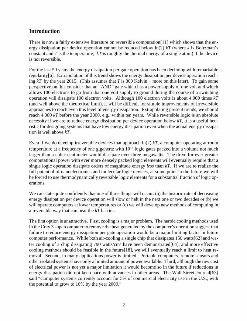
Several reversible devices have been proposed over the years. Von Neumann and independentlyGoto proposed the parametron[37] which encodes information in the phase of an oscillation. Fred-kin and Toffoli[23] proposed an electronic reversible logic family which used switches, capacitorsand inductors. By turning the switches on and off at just the right times, charge could be transferredbetween the capacitors through the inductors with minimal energy loss. By increasing the size ofthe inductors it would be possible to create a family of ever slower but ever more energy efficient
INPUT
OUTPUT
CONTROL Figure 1. An Electrostatic VoltageControlled Switch
Charged plate
Figure 2. Symbol for a Voltage Controlled Switch
INPUT
CONTROL
OUTPUT
5
circuits. As the LC time constant is increased, the energy dissipation can be decreased to an arbi-trary extent. A proposal by Likharev based on Josephson junctions[9, 10] “...is particularly signif-icant, because it is a genuine example ... of a system that has frictional forces proportional to ve-locity” according to Landauer[6]. The parametric quantron is based on Josephson junctions andoperates at low temperatures. It should dissipate less than kT when operating at 4 kelvins and witha switching time of 1 nanosecond[9]. Modern “high temperature” superconductors might allowoperation at relatively high temperatures, including that of liquid nitrogen[45]. Even these temper-atures would still be a significant disadvantage. Molecular−scale mechanical reversible “rod log-ic” has been proposed by Drexler which should dissipate less than kT when operating at room tem-perature at a speed of 50 to 100 nanoseconds[2, 18]. Drexler’s proposal is also significantly small-er than the parametric quantron. While the ability to fabricate Drexler’s proposal is some decadesaway, it provides a good argument that molecular−scale reversible devices should be feasible.
Although the parametric quantron can be used in a reversible fashion to achieve low energy dissi-pation it uses magnetic fields to couple logic devices, requires low temperatures to operate and willlikely prove resistant to scaling to the molecular size range. By contrast, Drexler’s mechanical pro-posal might well prove smaller than even the smallest of future electronic devices. Mechanical de-vices depend fundamentally on the position of the nuclei of the atoms of which they are made. Theposition of the nucleus of an atom can be much more precisely known than the position of an elec-tron: quantum uncertainty in the position of the electron is much greater because the mass of theelectron is much smaller. If device function depends on the position of an electron then device sizewill be larger than if device function depends on the position of the nucleus. Such molecular me-chanical proposals will, however, almost certainly be slower because of the greater mass of the nu-clei of atoms as compared with the mass of electrons. In this paper we discuss simple methods ofusing relatively conventional electronic switching devices in a reversible fashion which can bescaled to a very small size. The methods described here allow a simple voltage−controlled switchto be used in a reversible manner, both to implement combinational logic and also to iterate an ar-bitrary reversible logic function. Other methods are feasible. For example, helical logic -- an el-egant form of reversible electronic logic -- has recently been proposed by Merkle and Drexler[67].
Voltage controlled switches of various types have long been used in electronic devices[56, 66].Not all voltage controlled switches are suitable for use in low energy designs because of their in-trinsic energy dissipation. Traditional relays actuated by electromagnets dissipate comparativelylarge amounts of energy. Even if a switch were suited for low energy operation it would still dis-sipate energy if it were turned on when there was a voltage across it. The abrupt rush of currentthat normally occurs when a switch is turned on would insure this. Most previous logic designsbased on switches operated in this manner (though the proposal by Fredkin and Toffoli[23] avoidsthis problem, and the proposal by Seitz et. al. [29] eliminates dissipative switch closures for com-binational logic, although not for sequential logic). The switch is turned on for the purpose ofdraining charge when the charge is no longer wanted. That is, a logic “1” might be encoded by acharge on a capacitor. Turning on a switch to drain away that charge would dissipate energy evenif the switch itself were perfectly non-dissipative.
A related but distinct line of research also emphasizes the importance of energy dissipation, butassumes that the losses involved in dissipatively switching a wire from one logic state to anotherare fixed and cannot be altered, e.g., that slowing the switching speed will not reduce energy dis-

6
sipation. Even assuming that this is true, clever design of the circuit can greatly reduce the numberof times it is necessary to take such a dissipative action[52, 65]. Further research which combinesboth this approach and the approaches described here would seem fruitful.
Even relatively recently some authors have argued that switching devices must fundamentally dis-sipate more than kT regardless of how slowly they operate[57]. It is worth noting, therefore, thatcharging and discharging a condenser need not dissipate the energy involved. For example, a sim-ple LC oscillator will repeatedly charge and discharge a condenser. Although the energy stored onthe condenser is 1/2 CV2, this energy need not be dissipated during a charge/discharge cycle. Ifthe Q of the circuit is high the energy dissipation per cycle will be small. In addition, the energydissipation of such an oscillator depends on frequency. By using larger condensers and inductorsthe frequency of operation can be slowed and the fraction of energy dissipated per cycle reduced(see Drexler[18] for a discussion of scaling laws). If all linear dimensions of a device are scaledin size in proportion to some characteristic length L then capacitance and inductance are propor-tional to L while frequency and resistance are proportional to 1/L. The Q of the circuit is propor-tional to L so the percentage of the total energy in the oscillator that is dissipated per cycle can bereduced simply by increasing all linear dimensions equally. Different scaling methods can producebetter results.
If we assume that a fixed capacitive load is charged through a fixed resistance by a voltage that isramped up over a period of time T, then the energy dissipated by the resistance is approximately1/2 CV2 x 2RC/T (for RC << T). This dissipation can be reduced as much as we might want byincreasing T (and leaving the circuit components unchanged). Koller and Athas[61] have calledthis adiabatic charging[61]. We will call it “thermodynamically reversible” or simply “reversible,”relying on context to make it clear that we are referring to an asymptotically non-dissipative pro-cess. Note that the term “reversible” can also be used to mean “logically reversible” with no im-plication that it is asymptotically non-dissipative. A logically reversible process might be highlydissipative, so it is sometimes necessary to distinguish between “logically reversible” and “ther-modynamically reversible.” The term “reversible” in this paper will usually mean “thermodynam-ically reversible and asymptotically non-dissipative.” The reversible charging of a condenser isillustrated in figure 3.
The situation is quite different for a step function in which the voltage is ramped up instantly (T=0).This process dissipates 1/2 CV2. Charge falls through the fixed potential drop in a dissipative fash-ion much as water goes over Niagra falls. This is illustrated in figure 4. Although this is the meth-
Figure 3Power Dissipated is
1/2 CV2 x 2RC/T(for T >> RC)
T

7
od in common use today to charge and discharge the various capacitive loads in computer circuits,it is not the method that we will be considering.
Comparing figures 3 and 4 shows that the advantage of reversible charging is in the factor of2RC/T. Normally the switching time T must be longer than the RC time constant of the circuitsimply to insure that the output has time to settle to its proper value. By using reversible charging,further increases in the switching time can be used to decrease the energy dissipation per logic op-eration. This, of course, results in a slower speed of operation leading to a trade-off between speedand energy dissipation.
How to arrange matters so that current flows smoothly and reversibly is the principle topic of therest of the paper. This is challenging because the basic switching devices are (1) abrupt and dis-continuous and (2) pass through a dissipative intermediate state (which is neither fully on nor fullyoff) while switching.
The First Method
The first method uses a conventional voltage controlled switch but in a somewhat unusual manner.In essence we never turn a switch on or off when there is either a voltage across it or current goingthrough it. This mode of operation is reversible.
This approach has previously been used to compute combinational functions e.g., appropriatelyimplemented pass logic[55, 57] or CMOS transmission gates[53]; see Seitz et. al.[29] for a descrip-tion of hot clock nMOS. We extend this approach to implement a sequential circuit which can it-erate the computation of a reversible logic function. Several authors have pursued this approachrecently, including van de Snepscheut[60], Koller and Athas[61], and Hall[21], and have reachedsimilar conclusions. It is also related to “dry switching,” a method for using relays which avoidsturning relays on or off when there is a voltage across them[68]. The primary purpose of dryswitching is to avoid deterioration of the relay contacts, rather than minimize switching energy.
Conceptually, a voltage controlled switch can be thought of as a relay which is controlled electro-statically, as illustrated in Figure 1. We adopt the symbol shown in Figure 2 for a voltage con-trolled switch. We also adopt the following convention for turning a switch on and off: when thecontrol input to the switch is at logic “0” (low) the switch is turned on and current can flow fromthe input to the output or from the output to the input. When the control input is “1” (high) theswitch is turned off and current cannot flow.
Figure 4Power Dissipated is
1/2 CV2

8
The reader should note that this convention is not the usual one. We adopt it instead of its opposite−−where a “1” turns the switch on and a “0” turns it off−− because it is more intuitive when appliedto the second proposal discussed later in this paper, the CCD−based reversible logic element.
The proposed mode of operation is fundamentally clocked and multi−staged. The outputs of stagei drive the inputs of stage i+1. For the moment, we assume the output of stage 0 is simply given.That is, a set of input lines are assumed to have fixed voltages upon them representing the inputdata. The value of the succesive logic levels can then be computed in turn. The logic values (volt-ages) produced by stage 1 are computed from the logic values given by stage 0; The logic valuesproduced by stage 2 are computed from the logic values produced by stage 1; etc. etc.
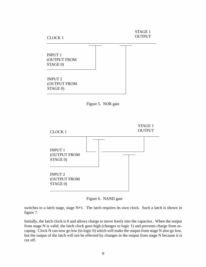
Simple pass logic can be employed to implement combinational logic. A “NOR” operation in thislogic is simply two switches in series. A clock signal (initially at logic 0) is connected to the inputof the first switch. If the control inputs of both switches have settled to logic 0, then both switcheswill conduct. The clock input connected to the first switch is slowly raised (from logic 0 to logic1). Both switches will conduct and the output will gradually shift to a logic 1. If either input is 1,one of the switches will not conduct and the output will remain at 0. Because the clock signal canbe raised and lowered slowly and reversibly, energy dissipation can in principle be made as smallas desired for this operation simply by slowing down the speed with which we clock the circuit. Asimple “NOR” gate is illustrated in figure 5. A “NAND” gate is illustrated in figure 6.
Making an N−level Circuit
We assume that we have an N level combinational circuit, and that N “clock signals” are provided.Initially, clocks 1 through N are low (logic 0), and the outputs of stage 0 are at some preset values.The outputs from stage 1 are computed as simple logical functions from the outputs of stage 0. Theoutputs from stage i are used as the inputs to stage i+1. A “NOR” and “NAND” gate from stage 1are shown in Figures 5 and 6. The NAND gate is logically complete so any arbitrary boolean func-tion can be implemented by using an appropriately connected collection of them.
The clock signals are now raised in turn. The output of “stage 0” is assumed to be valid prior tothe start of operations, and clock 0 is unspecified (for now). Clock 1 is raised, and the outputs fromstage 1 become valid. Clock 2 is raised, and the outputs from stage 2 become valid. This sequencecontinues, until clock N is raised, and the outputs from stage N become valid.
A single stage in the N level circuit could in principle implement an arbitrary boolean switchingfunction by an appropriate arrangement of switches. This might require an exponential number ofswitches and so multiple stages appear to be useful. Also, although for simplicity we have assumedthat the outputs of stage i are used directly only in stage i+1, they could equally be used in stagesi+2, i+3, etc. We will not consider these additional complexities here because they are secondaryto the fundamental issues.
Latches
What has been described so far will allow the construction of an N level reversible combinationallogic circuit. To be useful, we must also specify a latch which can store the output of the circuit.This can be done by holding charge on a capacitor. The outputs of stage N are connected through
9
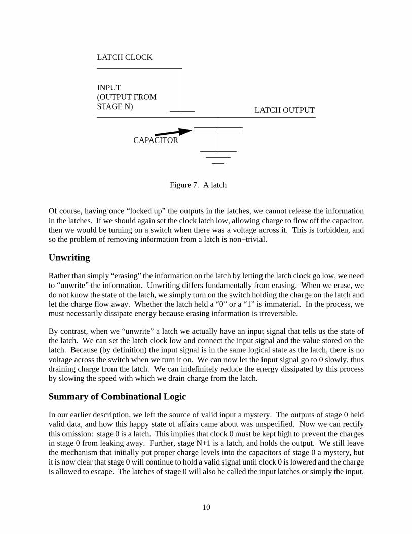
switches to a latch stage, stage N+1. The latch requires its own clock. Such a latch is shown infigure 7.
Initially, the latch clock is 0 and allows charge to move freely into the capacitor. When the outputfrom stage N is valid, the latch clock goes high (changes to logic 1) and prevents charge from es-caping. Clock N can now go low (to logic 0) which will make the output from stage N also go low,but the output of the latch will not be effected by changes in the output from stage N because it iscut off.
Figure 5. NOR gate
INPUT 2(OUTPUT FROMSTAGE 0)
INPUT 1(OUTPUT FROMSTAGE 0)
STAGE 1OUTPUTCLOCK 1
Figure 6. NAND gate
INPUT 2(OUTPUT FROMSTAGE 0)
INPUT 1(OUTPUT FROMSTAGE 0)
STAGE 1OUTPUTCLOCK 1
10
Of course, having once “locked up” the outputs in the latches, we cannot release the informationin the latches. If we should again set the clock latch low, allowing charge to flow off the capacitor,then we would be turning on a switch when there was a voltage across it. This is forbidden, andso the problem of removing information from a latch is non−trivial.
Unwriting
Rather than simply “erasing” the information on the latch by letting the latch clock go low, we needto “unwrite” the information. Unwriting differs fundamentally from erasing. When we erase, wedo not know the state of the latch, we simply turn on the switch holding the charge on the latch andlet the charge flow away. Whether the latch held a “0” or a “1” is immaterial. In the process, wemust necessarily dissipate energy because erasing information is irreversible.
By contrast, when we “unwrite” a latch we actually have an input signal that tells us the state ofthe latch. We can set the latch clock low and connect the input signal and the value stored on thelatch. Because (by definition) the input signal is in the same logical state as the latch, there is novoltage across the switch when we turn it on. We can now let the input signal go to 0 slowly, thusdraining charge from the latch. We can indefinitely reduce the energy dissipated by this processby slowing the speed with which we drain charge from the latch.
Summary of Combinational Logic
In our earlier description, we left the source of valid input a mystery. The outputs of stage 0 heldvalid data, and how this happy state of affairs came about was unspecified. Now we can rectifythis omission: stage 0 is a latch. This implies that clock 0 must be kept high to prevent the chargesin stage 0 from leaking away. Further, stage N+1 is a latch, and holds the output. We still leavethe mechanism that initially put proper charge levels into the capacitors of stage 0 a mystery, butit is now clear that stage 0 will continue to hold a valid signal until clock 0 is lowered and the chargeis allowed to escape. The latches of stage 0 will also be called the input latches or simply the input,
Figure 7. A latch
INPUT(OUTPUT FROMSTAGE N)
LATCH CLOCK
LATCH OUTPUT
CAPACITOR
11
while the latches of stage N+1 will also be called the output latches or simply the output.
We can now specify our initial state as one in which appropriate charges are held on the input, clock0 is high (to prevent charge from the input latches from leaking away), while clocks 1 through Nare held low; as is clock signal N+1 (that is, there are no charges held on the output latches and theswitch connecting the output latches to the final logic stage is turned on). We raise clock signals1 through N in turn, computing the values of each logic level in turn. Finally, we raise clock signalN+1, thus trapping the output signals in the output latches. We are then free to lower clock signalN, then N−1, then N−2, etc. until we have finally worked our way back to the first logic level.When the computation is done, all clock signals from 1 through N are held low, while clock signals0 and N+1 remain high. Charge is trapped in stage 0 corresponding to the input, and charge istrapped in stage N+1 corresponding to the output. The outputs of stage 0 and N+1 are valid. Allother outputs are 0.
Iteration of a Reversible Logic Function
At a higher level of abstraction, we can say that the outputs of stage N+1 are equal to some com-binational function F applied to the outputs of stage 0, or output = F(input). Of course, we’re nowstuck. We cannot unwrite the input latches because we don’t know what information is stored inthem.
We can solve this dilemma by requiring that F be reversible. That is, we demand that F-1(F(input))= input for all possible values of the input on stage 0. This allows us to compute the values storedin stage 0 from the values stored in stage N+1. We need merely compute F-1(output). That is, weadd additional logic stages N+2, N+3, ..., N+M which compute the inverse of F. The output ofstage N+M will then be the same as the input. Because we now have data values which are iden-tical to the contents of stage 0, we can unwrite stage 0 in a fully reversible fashion. That is, we canlower clock 0 and allow the charge on the capacitors in stage 0 to be connected with the outputsignals from stage N+M. Because they are identical the energy loss from this operation can bemade arbitrarily small. Then, clock signal N+M can be lowered, clock signal N+M−1 can be low-ered, etc. until we finally lower clock signal N+2. Clock signal N+1 (the latch control clock signalfor the output) is high (to hold the output steady in the output latches) and remains high.
To review the cycle of operations from the initial state: we start with a valid input in stage 0, withclock signal 0 held high (to hold the charge in the latches of stage 0) and with all other clock signalsheld low. From this intial state, we start the computation by raising clock signals 1 through N inturn, computing F(input). Clock signal N+1 is then raised to hold the output values in the outputlatches of stage N+1, and then clock signals N, N−1, N−2, ..., 1 are lowered in their turn to “un-compute” the calculation of F. We then compute F-1(output) by raising clock signals N+2, N+3,N+4, ..., N+M. This computation produces exactly the values that are stored in stage 0, and so wecan now unwrite the contents of stage 0 by lowering clock 0: this turns on the switches connectingthe latches of stage 0 to the output of stage N+M. We then uncompute the calculation of F-1(output)by succesively lowering clock signals N+M, N+M−1, N+M−2, ..., and N+2. Finally, we again raiseclock 0 to again isolate the input (which is now all 0).
At the end of this process the outputs are stored in stage N+1 and the input is all 0. The entire pro-
12
cess was carried out in a fully reversible manner, and so energy dissipation can in principle be madearbitrarily small. The only thing we need finally do is exchange the data in the input and outputlatches (we assume that the input and output latches have the same number of bits). To do this, wefirst transfer the data in the output latches into the input latches and then “unwrite” the output latch-es. While the circuitry for this is not entirely trivial, it should be clear that the principles developedshould allow us to do this. The sequence of steps involved is gone over in detail in the followingseveral paragraphs.
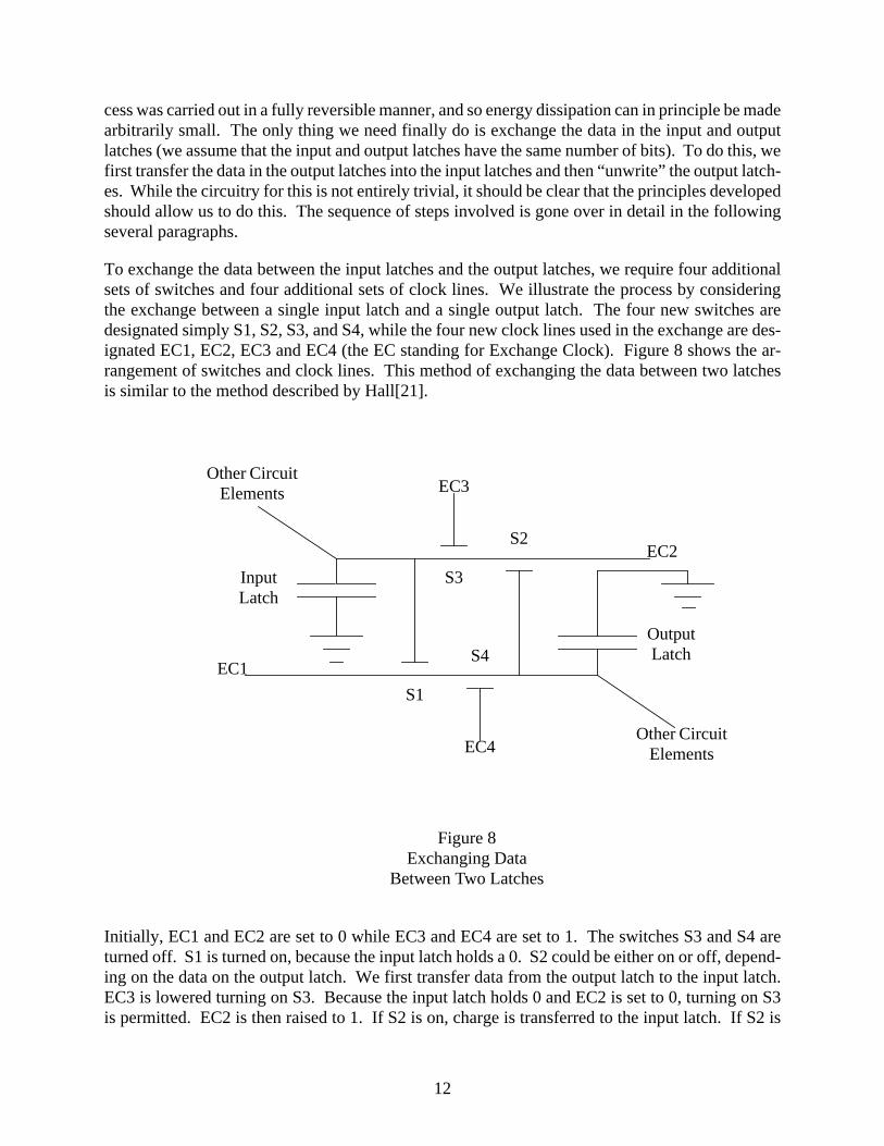
To exchange the data between the input latches and the output latches, we require four additionalsets of switches and four additional sets of clock lines. We illustrate the process by consideringthe exchange between a single input latch and a single output latch. The four new switches aredesignated simply S1, S2, S3, and S4, while the four new clock lines used in the exchange are des-ignated EC1, EC2, EC3 and EC4 (the EC standing for Exchange Clock). Figure 8 shows the ar-rangement of switches and clock lines. This method of exchanging the data between two latchesis similar to the method described by Hall[21].
Initially, EC1 and EC2 are set to 0 while EC3 and EC4 are set to 1. The switches S3 and S4 areturned off. S1 is turned on, because the input latch holds a 0. S2 could be either on or off, depend-ing on the data on the output latch. We first transfer data from the output latch to the input latch.EC3 is lowered turning on S3. Because the input latch holds 0 and EC2 is set to 0, turning on S3is permitted. EC2 is then raised to 1. If S2 is on, charge is transferred to the input latch. If S2 is
Figure 8Exchanging Data
Between Two Latches
Other CircuitElements
Other CircuitElements
EC2
EC1
EC3
EC4
S1
S2
InputLatch
OutputLatchS4
S3

13
off, charge is not transferred. Thus, if the output latch holds a 1 the input latch will be set to 0. Ifthe output latch holds a 0, the input latch will be set to 1. In the process of transferring the datafrom the output latch to the input latch, we have also inverted it. To correct this omission wouldrequire an inverter in the diagram of figure 8, or some modifications to F and F-1. This would takean additional switch and an additional clock line, as well as additional explanation. The figure,however, would rapidly become cluttered so we have chosen to omit the inverter to clarify the ex-position. This ommision has no impact on the basic concept.
Having set the input latch with data from the output latch, we now raise EC3 and turn off S3. Fi-nally, we lower EC2. This completes the transfer of data from the output latches to the input latch-es. We must now unwrite the output latches.
Unwriting the output latches is similar to setting the input latches, but the exact sequence of oper-ations is changed. Our first step is to raise EC1. We then lower EC4 turning on S4. EC1 is high,so if there is charge on the output latch then we have turned on a switch when there is no voltageacross it, which is permitted. If there is no charge on the output latch, then there will be charge onthe input latch (because we transferred the complement of the output latch to the input latch in theearlier steps) and this charge will turn off S1. Therefore, the output latch and EC1 will not be con-nected. Again, we have not turned on a switch with a voltage across it.
At this point, if the output latch is charged it is connected to EC1. By lowering EC1 we can drainthe charge from the output latch. We then raise EC4 turning off S4. This isolates the output latchagain and completes the unwriting of the output latch from the input latch.
The clocking sequence, in brief, is: lower EC3, raise EC2, raise EC3, lower EC2, raise EC1,lower EC4, lower EC1, raise EC4.
This sequence of operations has exchanged the data on the input latch and the output latch, and didnot require turning on a switch when there was a voltage across it. The careful reader might wonderabout the charge that might be trapped on the segment between S1 and S4 or between S2 and S3.These segments are initially 0, and are restored to 0 upon completion of all operations. During theactual transfer and unwriting steps, the charge on these segments is always known and does notresult in turning on a switch with a voltage across it. An explicit capacitance attached to this seg-ment would not alter the conclusions reached here for this specific design. In other designs it mightbe useful to eliminate such segments. Whether or not such segments can be eliminated depends onthe specific implementation. Elimination can often be done by appropriate physical design of theswitches, effectively resulting in a single switch with two control inputs.
We have now completed the full cycle of operations required to compute F(input). We can go onto compute F(F(input)), F(F(F(input))), etc. etc. We assume F is computationally useful (e.g., itimplements a single instruction or step of a reversible computation). As discussed earlier, revers-ible functions can be used to carry out arbitrary computations.
Problems with Inaccurate Voltage
While the system described is reversible in principle, the energy dissipation in a practical imple-mentation would depend upon the accuracy of the voltage. When a switch is turned on, the logical
14
state of the input and output values is the same, but the physical state might differ. A small differ-ence in the voltages at the input and output of the switch would result in energy loss as the switchwas turned on. Even with this restriction, it should be possible to achieve significant reductions inenergy dissipation. The energy dissipated by dissipatively discharging a capacitive load is
where C is the capacitance and V is the voltage. In conventional (irreversible) logic systems, thevoltage V would be the voltage of the power supply. In a reversible system of the type describedhere the voltage V would be the error in the voltage of the power supply, rather than the voltage ofthe power supply itself. Thus, by using reversible instead of irreversible logic, we have effectivelyreduced the value of V. With a power supply accurate to 5%, the energy losses from charging anddischarging the load capacitances associated with the electrical connections would be decreased bya factor of 202 or 400. That is, energy losses would be a function of the error in the voltage of thepower supply, rather than a direct function of the voltage of the power supply itself. There doesnot appear to be any reason in principle why the error in the voltage of the power supply could notbe made as small as desired.
A more fundamental reason for long term optimism is the observation that electric charge is quan-tized. In future systems in which the number of electrons that represents a logic “0” or “1” is bothfinite and small, it should be possible to reduce the energy loss caused by slight inaccuracies in thevoltage supply to 0. It is already possible to control the passage of individual electrons in a cir-cuit[4, 26, 69]. Such highly precise control should eventually make a fully reversible electronicswitch with extremely small energy losses feasible.
Problems with FETS: Voltage Degradation
Switching elements that do not degrade the voltage of the signal being switched are feasible in prin-ciple, as shown by the electrostatic relay illustrated in figure 1. CMOS transmission gates can alsobe used as switches without concern about voltage degradation. Transmission gates require thatboth the control signal and its inverse be provided. A simple method of satisfying this requirementwould be to use two−rail logic. To use nMOS (or pMOS) by itself, we must overcome certainshortcomings. In particular an nMOS switch, when used in pass logic, will cause voltage degra-dation. As a consequence, deterioration of the voltage through multiple logic levels would imposea severe limit on the capabilities of the system.
Boosting voltage in a fully reversible fashion is, however, straightforwards in principle. The volt-age on a capacitor will increase if the capacitance decreases. Variable capacitors are well knownbased both on physical motion of the capacitor plates, or on changes in charge distribution second-ary to a voltage change. Varactors in which the capacitance C changes by a factor of 10 or morein response to a voltage change of little more than a volt are feasible [25, 30]. The approach out-lined here is abstractly similar to the proposal by Joynson et. al.[28].
Boosting voltage is illustrated in figure 9. Before starting, the switch is turned on and current canflow onto the varactor. The high−voltage clock then opens the switch, trapping the charge on the
Energy12---CV2=

15
varactor. Finally, the capacitance of the varactor is reduced. Because the voltage on a capacitor is
(where V is voltage, Q is charge and C is capacitance) the voltage across the varactor will increaseas its capacitance decreases. Because the voltage on the high−voltage clock is large, there is morethan sufficient control voltage to insure that the switch remains turned off even though the voltageacross the switch has been increased. The low−voltage input, boosted to a medium−voltage output,can then be used to switch a low−voltage signal, which can again be used as the input to a reversiblevoltage booster.
To reverse this cycle of operations, the capacitance of the varactor is returned to its original value.This will also return the voltage on the output to its original value, and the high−voltage switch canbe turned on with minimal energy loss. This energy loss will be a function of the square of the errorin the voltage regulation. If the number of electrons that charge the varactor (and any stray outputcapacitance) is reduced to a small integer number, it should eventually be possible to eliminatelosses due to small inaccuracies in voltage regulation.
Seitz et. al. [29] commented that “...the isolation transistor can turn on while there is voltage acrossit, and accordingly, it dissipates power in charging or discharging the bootstrap node. The goal ofexporting all of the dynamic power is elusive.” Translating from their language to the languageused here, they sometimes allowed the high−voltage clock to turn on the high−voltage switch whena voltage existed across the switch, thus dissipating energy. They did not consider the computationof F-1 and “unwriting” operations, and so were sometimes obliged to engage in the dissipative op-eration of discharging the gate of a FET to ground. In essence, they were able to eliminate unnec-essarily dissipative operations for combinational logic, but not for sequential logic. As shown here,appropriate design of a reversible sequential circuit eliminates the unnecessarily dissipative steps.
Figure 9. A ReversibleVoltage Booster
LOWVOLTAGE
INPUT
HIGH VOLTAGECLOCK
VARACTOR
MEDIUMVOLTAGEOUTPUT
VQC----=
16
Problems with FETS: Leakage Current
Another problem with FET’s is leakage current. Even a FET in which the gate voltage is sufficientto insure that the FET is completely cut off will still pass a small current. If our objective is toachieve energy dissipations below kT, any significant leakage current is intolerable.
Leakage current occurs because thermally generated electron−hole pairs are created in the semi-conductor material of the FET. Thermal agitation will occasionally cause an electron in the valenceband (e.g., an electron which normally would not be able to move because it was fixed in place aspart of a covalent bond) to leap into the conduction band. An electron in the conduction band isfree to move throughout the crystal and so to conduct electric current. The energy gap between thevalence band and the conduction band will govern the concentration of electrons that are availableto carry leakage current. In silicon, the bandgap is 1.12 electron volts. At 300 kelvins, this willproduce 1.45 x 10¹⁰ electrons per cubic centimeter of silicon. This “intrinsic carrier concentration”will result in dissipative energy losses.
Three obvious methods are available for reducing the leakage current:
(1) Reduce the physical size of the device. An intrinsic carrier concentration of 1.45 x 10¹⁰ elec-trons per cubic centimeter can also be expressed as 1.45 x 10⁻¹¹ electrons per cubic nanometer. Ifthe active region of the device was smaller than a few millions of cubic nanometers, then the prob-ability of finding an undesired charge carrier in that region would be relatively small.
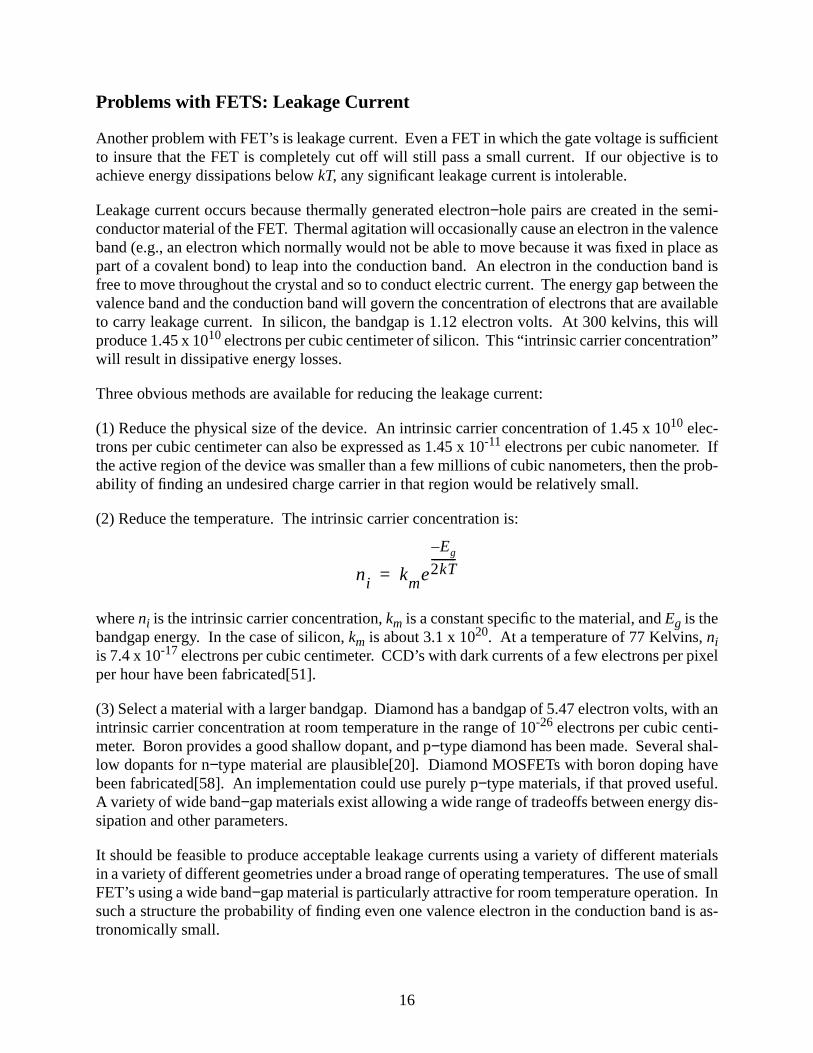
(2) Reduce the temperature. The intrinsic carrier concentration is:
where ni is the intrinsic carrier concentration, km is a constant specific to the material, and Eg is thebandgap energy. In the case of silicon, km is about 3.1 x 10²⁰. At a temperature of 77 Kelvins, niis 7.4 x 10⁻¹⁷ electrons per cubic centimeter. CCD’s with dark currents of a few electrons per pixelper hour have been fabricated[51].
(3) Select a material with a larger bandgap. Diamond has a bandgap of 5.47 electron volts, with anintrinsic carrier concentration at room temperature in the range of 10-26 electrons per cubic centi-meter. Boron provides a good shallow dopant, and p−type diamond has been made. Several shal-low dopants for n−type material are plausible[20]. Diamond MOSFETs with boron doping havebeen fabricated[58]. An implementation could use purely p−type materials, if that proved useful.A variety of wide band−gap materials exist allowing a wide range of tradeoffs between energy dis-sipation and other parameters.
It should be feasible to produce acceptable leakage currents using a variety of different materialsin a variety of different geometries under a broad range of operating temperatures. The use of smallFET’s using a wide band−gap material is particularly attractive for room temperature operation. Insuch a structure the probability of finding even one valence electron in the conduction band is as-tronomically small.
ni kme
Eg–
2kT---------
=
17
Thermally generated leakage current is also of concern in many types of varactors. A reverse−bi-ased P−N junction illustrates the problem: electron−hole pairs generated thermally in the chargedepletion region are swept out of the region, thus conducting current. Leakage current in such var-actors can in principle be made quite small for the same reasons that apply to leakage current in aFET.
Reversible CCD−Based Logic
An alternative approach, which eliminates the need for high accuracy voltage supplies, is to elim-inate the need to turn on the switch when there are charge carriers present. This might be viewedas only turning the switch on and off when the voltage across the switch is 0 volts, but this is not afully adequate description. Even a 0 volt signal is subject to fluctuation and noise. If, however, wetry to put a positive voltage onto the switch (e.g., the inputs and outputs of the switch both have apositive voltage), and if the charge carriers in the switch are electrons, then it is possible to removeall the charge carriers from the channel region. Any charge carriers will be actively swept out ofthe channel region by the positive voltages on the input and output leads. Once all the charge car-riers have been removed from the channel region, then no more current will flow. Precise regula-tion of the positive voltage on the input and output of the switch is not required, for both needmerely be “sufficiently positive” to insure removal of all charge carriers from the channel region.Once the charge carriers have been removed then turning the switch on and off can be done in afully reversible manner. Small errors in the supply voltage can no longer lead to dissipative currentflows when the switch is turned on, because no current can flow.
For purposes of this discussion we will assume our switch is a FET with electrons as the chargecarriers and that the electrons are removed from the FET by a positive voltage on the input andoutput leads. (We could equally well have assumed the charge carriers are holes and that a negativevoltage is placed on the input and output leads: for purposes of explanation the choice is arbitrary).As discussed earlier, it is essential that the device be designed so that the concentration of intrinsiccharge carriers is sufficiently low that energy losses from this source can be neglected. Further, thedensity of device defects must be low enough that defect sites do not appreciably alter device per-formance. We will simply assume that the material is free of defects. Reduction of device sizecoupled with decreases in defect rates should eventually allow construction of devices with a suf-ficiently low defect rate that energy dissipation will not be significantly degraded.
In this approach, 1’s and 0’s are represented by a packet of electrons or the absence of a packet ofelectrons, respectively. The electrons are stored in potential wells which we will call “buckets.”Each packet of electrons is treated as a unit: we never split or merge packets, nor do we create ordestroy packets (except when the system is initialized, which would ideally occur only once).While all packets have approximately the same number of electrons, it is not critical that each pack-et have exactly the right number of electrons. Whether a packet has 99, 100, or 101 electrons won’tmatter.
The use of charge packets is most familiar in the context of CCDs (Charge Coupled Devices)[47,50], or alternatively in the context of BBD’s, or Bucket Brigade Devices[49]. In a CCD, chargepackets are transferred from potential well to potential well serially along a row of devices. Theamount of charge in each packet is a measure of some analog quantity. Such devices are primarilyused as memory elements or shift registers, not for computation. Proposals to use the same basic
18
concepts for logic operations have been made since the invention of the CCD[34, 35, 36, 46, 48].Sometimes called “DCCL,” or Digital Charge Coupled Logic, these proposals have explored theadvantages of using charge packets as the basic logic element. The primitive logic elements in pri-or proposals, however, were highly dissipative. For example, Zimmerman et. al.[34] proposed log-ic operations whose computation required merging packets, discarding packets by draining thecharge to ground, etc. The goal of thermodynamically reversible logic was not an objective.Tompsett[48] proposed circuits in which the potential generated by a charge packet in a CCD po-tential well was coupled to the gate of a FET. This FET would then be turned on or off dependingon whether a charge packet was present or absent in the potential well. This was then used to createanother charge packet (rather than to control the movement of an existing charge packet). The cre-ation of a new charge packet would compensate for imperfect charge transfer. NAND and NORoperations could be performed by applying the potential from two potential wells to two gates oftwo FETs, which could then be connected in serial or parallel. Again, the objective of thermody-namic reversibility was not considered. The method of sensing charge in the potential well wasdissipative and the sensed packets, no longer needed, were to be dissipatively discarded.
For simplicity, we will assume that packets never gain or lose electrons (due to defects in the ma-terial or to thermal noise). In fact, present day devices can gain or lose charge at the rate of a fewparts per million[51]. As discussed earlier, such gains or losses should eventually be reduced toinsignificant levels. Even if we allow packets to gain or lose electrons at some low rate, we couldperiodically “refresh” the packets, and so prevent malfunction. Tompsett[48] first proposed meth-ods of refreshing packets (though he did not consider reversible methods). To the extent that thepacket has gained or lost an unpredictable amount of charge, “refreshing” the packet must funda-mentally dissipate energy. Other than this fundamental loss, however, we wish to keep energy dis-sipation to a minimum. A reversible method of refreshing a packet would be to use the old packetto charge a bucket in a reversible fashion (as discussed in the first method), and then to “unwrite”or discharge the bucket holding the old packet by using the new packet as the source of informa-tion. This method of refreshing a packet would, of course, dissipate energy as a function of theerrors in the voltages involved (as discussed earlier). If the refresh operations were done infre-quently (e.g., a packet would be refreshed only after a large number of logic operations) then theenergy dissipation per logic operation from this source would be quite small.
While CCD and DCCL circuits are today implemented on a semiconductor surface using planartechnology, for purposes of this discussion we will initially ignore this geometrical constraint andinstead focus on more fundamental issues. A planar version of the ideas described here is given inthe section on “A Planar Version of RCT Logic.”
Figure 10 illustrates the “hydraulic” model[1] of charge transfer in a CCD. Charge is transferredfrom one potential well to the next much like water would flow to a gradually sinking region in apond. This process can be thermodynamically reversible when appropriately implemented.
One aspect of figure 10 might be slightly misleading. While water has a sharply defined surface,the energy of an electron at some non-zero temperature T is statistical. While figure 10 might leadone to conclude that extremely small perturbations in the potential might cause significant changesin the pattern of charge flow, in fact thermal noise will allow electrons to surmount small barrierse.g., where the barriers have a potential similar in magnitude to kT/e or .026 volts at room temper-ature (where e is the charge on an electron). Small perturbations and errors in the potential do not

19
fundamentally create dissipative problems.
Tranferring Charge With Little Dissipation
Before discussing the more complex operations needed for computation, we first consider a simple
Figure 10Hydraulic Model of Charge Transfer
in a CCD (Adapted from Sze[1])
5 volts 10 volts 5 volts
Silicon Dioxide
5 volts 10 volts 12 volts
Silicon Dioxide
p-Si
Negative Charge(electrons)
5 volts 10 volts 15 volts
Silicon Dioxide
p-Si
p-Si

20
sequence that transfers charge from a source bucket to a destination bucket with as little energy lossas desired. This is illustrated in figure 11 . (Note that the illustration shows that the two buckets
have semiconductor plates joined by a semiconductor path. The use of metallic plates or a metallicconnection between the two plates would cause unwanted energy dissipation). At first, both thesource clock and destination clock are + (positive), and the charge packet is entirely in the sourcebucket. The clocking sequence will then shift the charge from the source bucket to the destination
+
+
-
-
+
+
-
-
+
+
----
----
- - - -
----
----Charge
Distribution
1 +
2 +
3 −
4 −
5 +
+
−
−
+
+
----
----
- - - -
----
----Charge
Distribution
Figure 11Transferring Charge
With Little Dissipation
SOURCE DESTINATION
SourceClock
DestinationClock
SemiconductorRegion
21
bucket in a series of steps, where each step can dissipate an arbitrarily small amount of energy. Aswe move from state 1 to state 2, the destination clock is changed from + to −. This change resultsin negligible energy dissipation, because no charge can move at this time. As we move from state2 to state 3, the source clock is changed from + to −. The charge carriers in the charge packet (elec-trons in our example) now move out of the source bucket. Because the destination clock is nega-tive, the electrons will migrate smoothly out of the source bucket. (If the destination clock were +at this point instead of −, the electrons would move out of the source bucket and then “fall downhill” into the destination bucket, dissipating energy). As we move from state 3 to state 4, the des-tination clock changes from − to +, thus slowly attracting the electrons and gathering them into thedestination bucket. Finally, as we move from state 4 to state 5, the source clock changes from − to+ restoring the system to its original condition, but with the charge packet in the destination bucketinstead of the source bucket.
The primary source of energy dissipation in this sequence is from state 2 to state 3, and from state3 to state 4. These transitions involve charge migration, and will therefore result in dissipative loss-es. As we slow the clock frequency the clock voltages change more slowly, the charges move moreslowly, and hence dissipate less energy. Because energy dissipation is a function of the square ofthe current, reducing the frequency of operation by a factor of two will also reduce the current bya factor of two but will reduce the energy dissipation by a factor of 4. This will reduce the energydissipated per logic operation by a factor of 2. Thus, by sufficiently slowing the clock frequencywe can dissipate as little energy per operation as might be desired.
It is important to notice that these operations do not erase information. We start with a charge pack-et in a single potential well on the left, and we end with a charge packet in a single potential wellon the right. During the course of moving the charge packet we slowly change the shape and po-sition of the potential well, but at no point do we merge potential wells. The potential well at theright is initially empty, which is why the transition from step 1 to step 2 in figure 11 is allowed andnondissipative. This transition eliminates the right hand potential well without merging it with thewell on the left. An attempt to merge the two potential wells would be dissipative. The transitionfrom step 2 to step 3 slowly changes the shape of the potential well, but the charge packet is alwayscontained in a single potential well and is always at or near thermodynamic equilibrium within thatwell.
The Primitive Operation
We now consider the somewhat more complex operation that is required to support computation ina reversible fashion. The single primitive operation is:
Transfer charge out of a source bucket and into an empty destination bucket if a “condition” bucketholds a “0”, but do not transfer the charge if the condition bucket holds a “1”. If the transfer doesnot take place (the condition bucket is “1”), the destination bucket need not be empty.
“Empty” in this context means “has no charge carriers present.” That is, an “empty” bucket is inlogic state “0.”
We will call this device a 3-bucket Reversible Charge Transfer device, or (where context makes itclear which type of RCT we are referring to) simply an RCT. The RCT is a reversible DCCL de-
22
vice. At a logical level the RCT is related to (but somewhat different from) a switch gate[7, page241] implemented using charge packets instead of colliding billiard balls. The particular logicfunction described here is but one example of the range of logic functions that involve the revers-ible transfer of charge from one bucket to another. During normal operation, RCT devices (1) nev-er merge or split charge packets (2) never discharge charge packets to ground, and (3) move chargepackets in a thermodynamically reversible fashion from a set of source buckets to a set of destina-tion buckets, conditional on the presence or absence of charge in a set of condition buckets. In thiscontext thermodynamic reversibility means that energy dissipation per device operation, in the ab-sence of manufacturing defects, could be made much smaller than kT simply by slowing the speedof operation. The number of charge packets is conserved and therefore RCT devices are conser-vative logic devices (in conservative logic devices, the number of 1’s is conserved during the com-putation, so the number of 1’s at the input is the same as the number of 1’s at the output). We havedescribed the 3-bucket RCT, which has one condition bucket, one source bucket, and one destina-tion bucket. More complex RCT’s have more buckets and the pattern of charge transfer is morecomplex. Some of these RCT’s will be considered later.
The simple 3-bucket RCT operation might be written in C as:
if (Condition==0) Destination = Source; Source = 0;
while a somewhat briefer notation would be:
If Condition is 0 then Destination = Source.
(Note that in this briefer notation, the “=” sign is used to indicate both the assignment of the Sourcevalue to the Destination, and setting the Source to 0 after the assignment).
The precondition that must be true prior to execution of the 3−bucket RCT is:
(Destination==0) OR (Condition==1)
Violation of this precondition would result in an unwanted dissipative step, which is banned inRCT devices. While it might at first seem that satisyfing this precondition would make the 3−buck-et RCT data dependent, it is in fact possible to design a circuit in which we know that the precon-dition is satisfied without knowing what values are presented as inputs to the circuit.
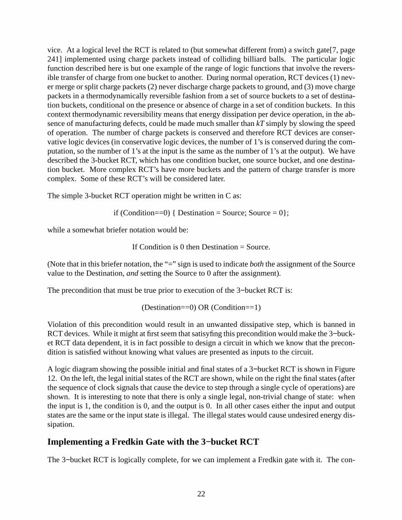
A logic diagram showing the possible initial and final states of a 3−bucket RCT is shown in Figure12. On the left, the legal initial states of the RCT are shown, while on the right the final states (afterthe sequence of clock signals that cause the device to step through a single cycle of operations) areshown. It is interesting to note that there is only a single legal, non-trivial change of state: whenthe input is 1, the condition is 0, and the output is 0. In all other cases either the input and outputstates are the same or the input state is illegal. The illegal states would cause undesired energy dis-sipation.
Implementing a Fredkin Gate with the 3−bucket RCT
The 3−bucket RCT is logically complete, for we can implement a Fredkin gate with it. The con-
23
struction used here is related to (though diffrent from) that used by Fredkin and Toffoli[7] for con-structing a billiard ball Fredkin gate from a billiard ball switch gate.
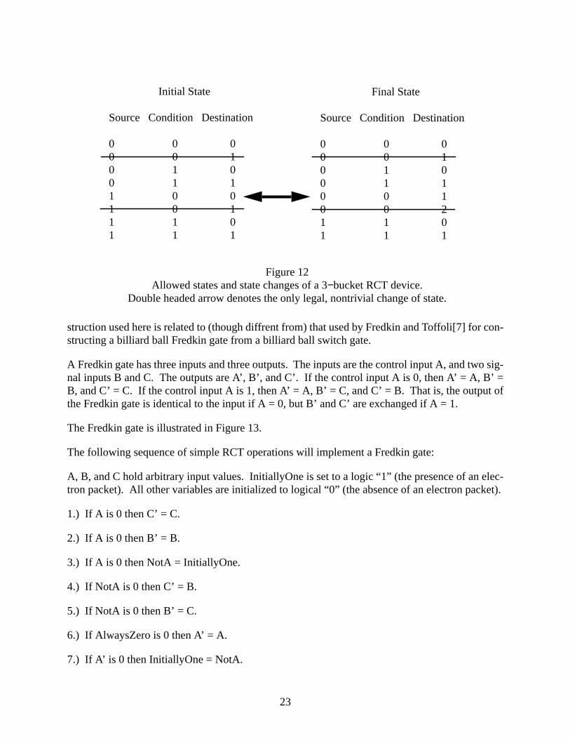
A Fredkin gate has three inputs and three outputs. The inputs are the control input A, and two sig-nal inputs B and C. The outputs are A’, B’, and C’. If the control input A is 0, then A’ = A, B’ =B, and C’ = C. If the control input A is 1, then A’ = A, B’ = C, and C’ = B. That is, the output ofthe Fredkin gate is identical to the input if A = 0, but B’ and C’ are exchanged if A = 1.
The Fredkin gate is illustrated in Figure 13.
The following sequence of simple RCT operations will implement a Fredkin gate:
A, B, and C hold arbitrary input values. InitiallyOne is set to a logic “1” (the presence of an elec-tron packet). All other variables are initialized to logical “0” (the absence of an electron packet).
1.) If A is 0 then C’ = C.
2.) If A is 0 then B’ = B.
3.) If A is 0 then NotA = InitiallyOne.
4.) If NotA is 0 then C’ = B.
5.) If NotA is 0 then B’ = C.
6.) If AlwaysZero is 0 then A’ = A.
7.) If A’ is 0 then InitiallyOne = NotA.
Figure 12Allowed states and state changes of a 3−bucket RCT device.
Double headed arrow denotes the only legal, nontrivial change of state.
Initial State
Source Condition Destination
0 0 00 0 10 1 00 1 11 0 01 0 11 1 01 1 1
Final State
Source Condition Destination
0 0 00 0 10 1 00 1 10 0 10 0 21 1 01 1 1
24
Steps 1 and 2 simply transfer charge from B and C into B’ and C’ if A is 0. B’ and C’ are initiallyempty, so this transfer satisfies the RCT preconditions.
Step 3 computes the logical negation of A and leaves that logical negation in “NotA.”
Steps 4 and 5 transfer charge from B and C into C’ and B’, exchanging the outputs. The precondi-tion is satisfied, for if A is 0, then NotA will be 1 and the transfer will not take place. If the transferdoes not take place, the prior contents of B’ and C’ are irrelevant. If A is 1, then NotA will be 0and the transfer will take place. In this case, B’ and C’ will be empty (have logic values 0) and sothe transfer will take place correctly.
B
C C’ = C
B’ = B
A’ = 0A = 0
B
C C’ = B
B’ = C
A = 1 A’ = 1
Figure 13A Fredkin Gate

25
Step 6 copies A into A’ unconditionally.
Step 7 restores the value of InitiallyOne if it was altered during the computation.
This implementation of a Fredkin gate will take three arbitrary input values and, after a sequenceof RCT operations, produce three output values. We could clearly apply N Fredkin gates to 3Ninput values and produce 3N output values at the same time. We require that all output values beinitially 0. After finishing the sequence of clocking operations, the inputs are all 0 and the outputshold arbitrary values. At this point, the “input” and “output” can be logically exchanged (e.g., nophysical operation takes place, but we relabel the “input” variables as “output,” and the “output”variables as “input”). Following this logical exchange, we have reestablished the preconditions forthe next sequence of operations: the (just relabeled) inputs again hold arbitrary logic values, whilethe (just relabeled) outputs hold logic 0’s. We now drive a (different) set of clock lines to apply the(different) Fredkin gates to generate the next “state” of the computation.
Viewed globally, this is a “ping-pong” or “double buffer” scheme for computing successive valuesof the global state of the system. If we call the two sets of variables A and B, and we call the twologic functions for the “next state” of the system F and G, then we first compute B=F(A). B is ini-tially all zeroes, while A holds arbitrary logic values. On completion of the computation of F, A isall zeroes while B holds arbitrary logic values. We then compute A=G(B). Because G uses B asits input and A as its output, the condition that the outputs be all zeroes is met during the compua-tion of G. This returns us to the state where A holds arbitrary logic values and B holds all zeroes.We can repeat this cycle indefinitely.
Implementation of a 3−bucket RCT
A planar layout of a 3−bucket RCT is shown in figure 14. Many kinds of implementations wouldbe feasible, for example Silicon−On−Insulator technology (the FET used for the transfer switchwould be “tilted on its side” in this approach). Note that many of the conductive paths are reallysemiconductors. Each bucket also has one semiconductor plate. The gate is also a semiconductor.Use of metallic wires for these components would compromise device function. A planar RCT isdescribed in a later section.
This RCT can be viewed as a combination of three CCD potential wells and a FET. A charge pack-et is first transferred from the “condition” potential well to the gate of the FET. The charge packetin the “source” potential well is then moved to the source of the FET and (the charge on the gateof the FET permitting) through the channel and out the drain of the FET into the “destination” po-tential well.
Tompsett[48] proposed sensing the presence or absence of a charge in a CCD potential well by con-necting the potential well via a doped region connected ohmically to a metalization that becamethe gate electrode of a FET. Charge injection from the gate into the doped region, while small ifthe capacitance of the gate is small, still introduces an unwanted source of energy dissipation. Oth-er aspects of Tompsett’s proposal were also irreversible or highly dissipative. In the present pro-posal, we require that both the gate of the FET and the connecting path from the potential well to
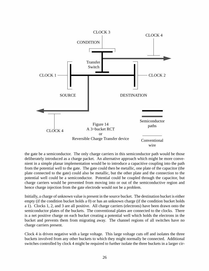
26
the gate be a semiconductor. The only charge carriers in this semiconductor path would be thosedeliberately introduced as a charge packet. An alternative approach which might be more conve-nient in a simple planar implementation would be to introduce a capacitive coupling into the pathfrom the potential well to the gate. The gate could then be metallic, one plate of the capacitor (theplate connected to the gate) could also be metallic, but the other plate and the connection to thepotential well could be a semiconductor. Potential could be coupled through the capacitor, butcharge carriers would be prevented from moving into or out of the semiconductive region andhence charge injection from the gate electrode would not be a problem.
Initially, a charge of unknown value is present in the source bucket. The destination bucket is eitherempty (if the condition bucket holds a 0) or has an unknown charge (if the condition bucket holdsa 1). Clocks 1, 2, and 3 are all positive. All charge carriers (electrons) have been drawn onto thesemiconductor plates of the buckets. The conventional plates are connected to the clocks. Thereis a net positive charge on each bucket creating a potential well which holds the electrons in thebucket and prevents them from migrating away. The channel regions of all switches have nocharge carriers present.
Clock 4 is driven negative with a large voltage. This large voltage cuts off and isolates the threebuckets involved from any other buckets to which they might normally be connected. Additionalswitches controlled by clock 4 might be required to further isolate the three buckets in a larger cir-
Figure 14A 3−bucket RCT
orReversible Charge Transfer device
CLOCK 1 CLOCK 2
CLOCK 3CLOCK 4
CLOCK 4
SOURCE DESTINATION
CONDITION
Semiconductorpaths
Conventionalwire
Transfer Switch
27
cuit, but are not shown in this small example. The two gray channels do not actively participatein the process of reversible charge transfer, they are present merely to show that connections to oth-er circuit components will be present in a real system.
Clock 3 is driven negative, forcing charge from the condition bucket onto the gate of the transferswitch. If no charge is present on the condition bucket, no charge will be put onto the transfer gate,while if charge is present then it will be transferred to the transfer gate, cutting off the transferswitch. Note that the circuit is so arranged that only a medium voltage will be developed on thetransfer gate, and this medium voltage can be contained by the high voltage of the cut off clock,clock 4.
Clock 2 is driven negative. If there is charge on the destination bucket, then the transfer switch isturned off and the charge on the destination bucket goes nowhere. If there is no charge on the des-tination bucket, then whether the transfer switch is turned off or on is immaterial, for no charge willbe transferred.
Clock 1 is driven negative. If the transfer switch is turned off, no charge will be transferred. If thetransfer switch is turned on, charge will move gradually through the transfer switch into the desti-nation bucket. Because clock 2 is negative, charge will not “fall down hill” in a dissipative fashionwhen moving into the destination bucket. Clock 1 has a low voltage so a low voltage is generatedduring the transfer operation. The medium voltage on the transfer gate is sufficient to block chargetransfer if charge transfer is not supposed to take place.
Clock 2 is driven positive, allowing charge to flow smoothly into the destination bucket. Whenclock 2 reaches its full positive value, all the charge is held on the destination bucket and no chargecarriers are present in either the source bucket or the transfer switch channel region (if the transferswitch was turned on).
Clock 1 is driven positive, which has no effect if the transfer took place and simply allows thecharge to return to its original state if the transfer did not take place.
Clock 3 is driven positive, allowing the charge on the transfer gate to return to the condition bucket.
Clock 4 is driven positive, opening the cut off switches that isolated the three buckets from outsideinfluence during the reversible transfer operation.
This cycle of operations reversibly transfers charge from the source bucket to the destination buck-et if the condition bucket holds a logic “0” (e.g., no charge).
Energy Loss
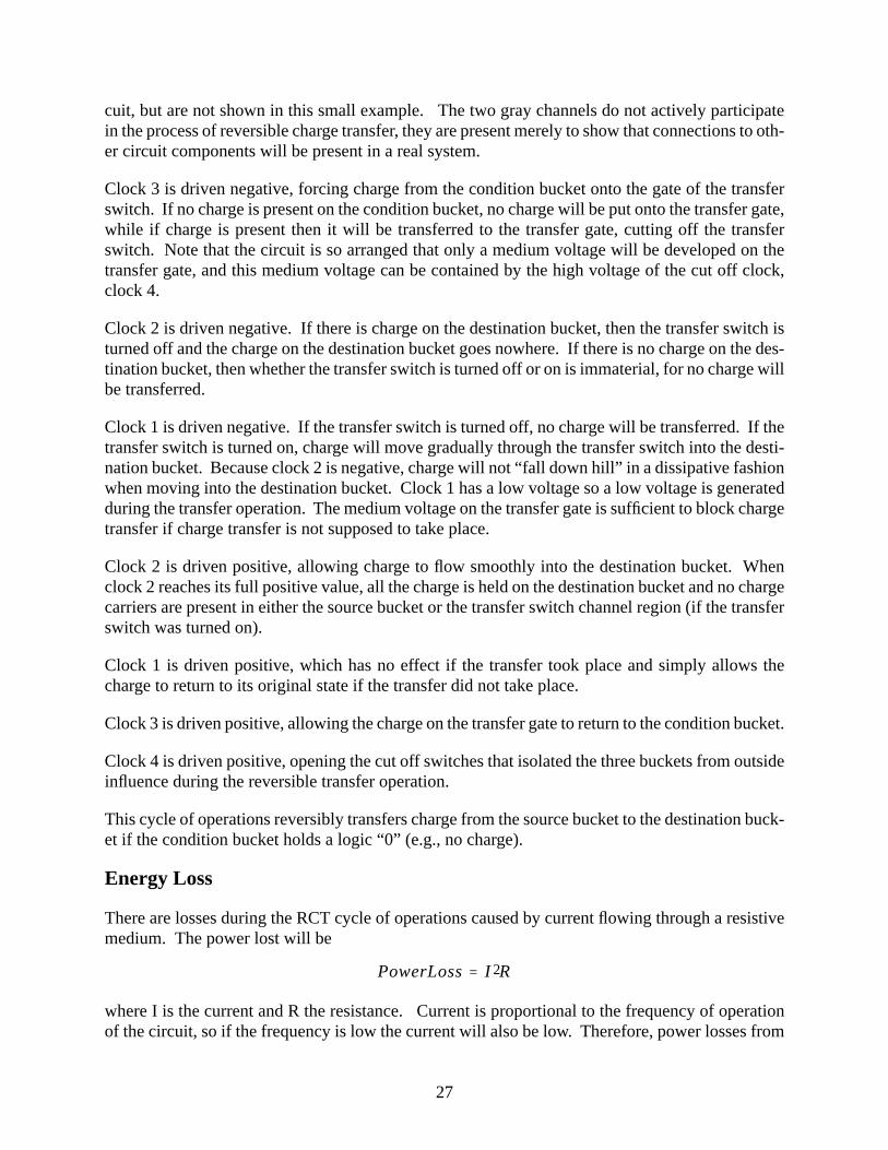
There are losses during the RCT cycle of operations caused by current flowing through a resistivemedium. The power lost will be
where I is the current and R the resistance. Current is proportional to the frequency of operationof the circuit, so if the frequency is low the current will also be low. Therefore, power losses from
PowerLoss I 2R=
28
resistive losses will fall off with the square of the frequency:
Because the number of operations per second is also lower at a lower frequency, the actual energyloss per device operation is proportional to the frequency of operation:
By reducing the frequency of operation, the energy loss per operation can be reduced to whateverextent is desired. It should be remembered that “low frequency” operation is relative: CCD’s with0.9997 charge transfer efficiency operating at 1 gigahertz have been demonstrated[54].
More specifically, the electron drift velocity vd equals the electric field E times the mobility µ:
If we let d be the distance traveled by an electron as it moves from one bucket to the next, and t bethe time of a single logic operation, then it is approximately the case that:
The total energy dissipated by the movement of n electrons as they move from the source to thedestination is simply the force times the distance times the number of electrons, or:
where Edissipated is the energy dissipated, n is the number of electrons in a packet, and e is thecharge of an electron.
Putting these together yields:
If we assume that the distance traveled by the charge packet as it moves from one bucket to the nextis .1 microns (10-5 centimeters), that one packet has 100 electrons, that the mobility is1800 cm2/V−s (the approximate mobility of diamond or silicon near room temperature), that thetime allotted for one operation is 1 nanosecond, and the charge e on an electron is 1.6 x 10⁻¹⁹ cou-lombs, then the energy dissipated is approximately 10-21 joules.
This estimate is based on a classical model and involves some significant simplifications. Mostsignificantly, the mean free path will of necessity be less than .1 micron in a device whose maxi-mum dimension is .1 micron, and so the meaning of the electron mobility µ is somewhat obscured.A more detailed quantum analysis is essential as the size becomes smaller[44]. A rough approxi-
PowerLoss f 2∝
EnergyLoss f∝
vd Eµ=
d vdt=
Edissipated neEd=
Edissipatedned2
µt------------=
29
mation to such an analysis can be based on the observation that the resistance of the channel of asufficiently small FET (e.g., one in which the channel width is perhaps a few nanometers and onlya single transmission mode exists) is roughly half of h/e2, where h is Planck’s constant. This is afundamental unit of resistance of about 26KΩ. A packet of n electrons flowing in time t producesa current of ne/t. The power produced by such a current flow is I2R, while the energy dissipationper logic operation is I2R x t, or (ne/t)2 x h/(2e2) x t which simplifies to:
For a switching time t of 1 nanosecond and a packet size n of 100 electrons, this is 3 x 10-21 joulesfor each packet that is passed through the channel of the FET. Under the specific conditionsconsidered here this second approximation agrees at least in order of magnitude with the estimatebased on a classical model.
It is interesting to note that the two equations have significant differences. The resistance of thechannel in the classical case varies with the length of the channel. The length of the channel is lesssignificant in the nonclassical case. The size of the charge packet, n, also influences energy dissi-pation in different ways in the two cases. In the classical case, the energy dissipation is a functionof n rather than n2. In the classical case, two electrons drifting under the influence of the same elec-tric field in separate regions of the channel will dissipate twice as much energy as a single electron.In effect, the resistance has been halved because the number of charge carriers has been doubled.A similar effect would occur in a doped semiconductor if the doping density were doubled. If weassume a narrow channel that can only support a single transmission mode, however, then doublingthe size of the charge packet will cause more electrons to move through the same channel in thesame time period, with a resulting increase in interactions among the electrons. The reader shouldnote that no claim of universality or high accuracy is implied for either of the above equations.They are rough approximations that apply only under a limited range of conditions. These condi-tions need not, in general, be true. In particular, it would seem attractive to design devices in whichsingle electrons are always close to their ground state both during charge transport and duringswitching operations. This would occur if the electron were always confined in a time varying po-tential well of relatively small dimensions. Devices with this property should be feasible when weare able to manufacture devices of sufficiently small size[67]. This should have a favorable influ-ence on energy dissipation.
The major factor ignored in this analysis is the energy dissipated by the clock signals. Many meth-ods of providing periodic clocking pulses are possible. Three methods are discussed in the nextsection.
The mobility can be substantially increased by reducing the temperature. Mobilities greater than1,000,000 have been demonstrated in GaAs−AlGaAs HFET’s at around 10 K[1, page 298]. Whilethe impact of this is unclear when the device size is much smaller than the mean free path (whichoccurs with such high mobilities), it does mean that larger devices could be made which wouldhave very low energy dissipation.
The energy dissipation for this type of reversible electronic logic (as estimated here) is greater than
Edissipatedhn2
2t---------=
30
the dissipation of Drexler’s rod logic[18] operated at a cycle time of 100 picoseconds (some 10times faster than the 1 nanosecond considered here for the RCT). When RCT device operationusing single electrons becomes feasible[4], then energy dissipation using RCT’s would presumablybe reduced. Likharev’s parametric quantron has an energy dissipation which (when adjusted forthe temperature difference and the differing speeds of operation) is not as good as rod logic. Theparametric quantron also requires low temperature. Rod logic should work at room temperature.It is possible that mechanical molecular logic might have very favorable energy dissipation prop-erties at low temperature[16].
While it is premature to draw conclusions it is not obvious that electronic devices must necessarilyprove better than molecular mechanical devices in terms of energy dissipation at a given speed andtemperature of operation.
Clocking
To insure that overall energy dissipation is reduced we need a method of providing suitable clocksthat does not itself dissipate too much energy. We first consider a conceptually simple method ofproviding arbitrarily complex clock signals which can be made to dissipate as little energy as de-sired.
The loads presented to the clock in the proposals discussed here are purely capacitive. If we as-sume, for the moment, that the energy dissipated when a clock signal charges and discharges suchpurely capacitive loads is 1/2 CV2, then the only method of reducing the energy dissipation is toreduce the voltage. Assume, for the moment, that we want a clock signal to increase from 0 voltsto 5 volts. If we simply connect the clock line to a 5 volt source, then the energy dissipated will be1/2 CV2 = 12.5 C joules. If we have 10 voltage supplies, with voltages of 0.5, 1.0, 1.5, 2.0, 2.5,3.0, 3.5, 4.0, 4.5, and 5.0 volts, then we can successively connect our clock line to each voltagesupply in turn. The voltage to the clock line would then be stepped up in 0.5 volt increments, andso the energy dissipated by a single step would be 1/2 C(V/10)2 = 0.125 C (e.g., the energy dissi-pation per step is decreased by a factor of 100 because the size of the voltage step is decreased bya factor of 10).
To increase the voltage from 0 to 5 volts involves 10 steps, and so we will dissipate 10 x (0.125 C)or 1.25 C joules. This is 10 times smaller than the 12.5 C joules we would have dissipated usinga single 5 volt supply. Thus, be using 10 DC power supplies and switching the clock line succes-sively from one power supply to the next, we have reduced energy dissipation by a factor of 10.Clearly, we can reduce energy dissipation by a factor of N if we use N DC power supplies. Noticethat the larger we make N the more time we must take to increase the voltage from 0 to 5 volts.Each time we take a step in voltage we must wait somewhat longer than one RC time constant forthe voltage to settle at the new value. This settling time will remain about the same for each step,even as we decrease the size of the voltage step by increasing N. As N increases and the numberof steps increases, the total time taken for N steps will also increase.
This approach is very flexible because the clock waveform can rise and fall at arbitrary times.Complex clock signals can be easily generated.
There are many alternative clocking schemes. While the method just described is asymptotically

31
nondissipative if a sufficiently large number of DC power supplies are used, it still involves movingelectrons through wires to carry the clock signal throughout the circuit. This does not appear to bethe major limiting factor in energy dissipation when using today’s planar technology. However, ifin the future we use single electron logic devices, then moving large numbers of electrons over longdistances to provide the clock signals would seem inappropriate.
There are approaches to clock distribution which avoid the need to move charge through wires. Aconceptually simple approach is to provide clock distribution by the use of charges that are fixedto a rotating tube or disk. A facing disk or a smaller concentric drum would carry the logic circuit-ry. As the disk spun the charges fixed to its surface would move, but this motion would not involveelectrons flowing within a conductor. The electric charges on the surface of the disk would thenmove past the logic elements on the facing surface of the opposing disk, providing the repetitivevoltage changes required to clock the logic circuitry. In principle this method of moving chargeswould result in no conventional resistive losses at all because the charge would not be movingthrough a conductor. There would still be radiative losses caused by the acceleration of the chargedparticles, and electrostatic attraction and repulsion would produce forces between the charges onthe two disks which would lead to losses simply by alternately compressing and decompressing thematerial of the disk.
While this approach might not be attractive with current technology, it might prove attractive atsome point in the future if strong materials could be rotated at high speeds, thus providing a highinterfacial velocity between the two opposing surfaces; and the pattern of charges on the surfacecould be both precisely controlled and have high resolution. This should eventually be feasible[18,32], though whether or not it will prove competitive with other approaches is uncertain.
Another method of providing a time−varying electric field would be to use a simple rotating elec-tric field. Such a rotating electric field could then be used to clock the circuit. While the methodsdescribed here do not obviously lend themselves to such an approach, helical logic[67] uses suchrotating electric fields to drive thermodynamically reversible logic operations. Charge is transport-ed along a helix much as water is transported along an Archimedes screw. Single electron versionsof helical logic should eventually be feasible. Rotating electric fields can be provided by severalmethods, including cavity resonators or multiple LC oscillators connected to plates arranged in anappropriate pattern in space.
Other RCT’s
The 3−bucket RCT is not the only type of RCT that is useful. For example, if we use two conditionbuckets C1 and C2, and require that the charge packets in C1 and C2 be complementary (e.g., C1is the negation of C2); and if we use a single source bucket S and two destination buckets D1 andD2; then we can implement the primitive “Transfer charge from S to D1 if C1 is false, but from Sto D2 if C1 is true.” We will again need a pre−condition that effectively prevents the merging oftwo packets; we omit the precise statement of this precondition. This 5−bucket primitive is logi-cally complete (we leave this as an exercise for the reader) and has certain implementation advan-tages. It is illustrated in Figure 15. In particular, because both C1 and its complement C2 areavailable, we need only “steer” the charge in the source bucket to either of the destination buckets.We need not “bottle up” the charge on the source bucket in the event the transfer is not to take place(as occurs with the 3-bucket RCT). Because the charge packet in bucket S is guaranteed to move

32
to some destination bucket (either D1 or D2), the actual voltage that must be generated to preventthe charge from moving in the wrong direction is smaller than the voltage required in the simpleRCT to prevent the charge from transferring to its single destination bucket.
The same logic function could also be implemented in a somewhat different fashion by using a 4-bucket RCT with a single source bucket S, a single condition bucket C and two destination bucketsD1 and D2. This is illustrated in Figure 16. In this alternative implementation, the charge in C
Figure 15A 5−bucket RCT
Charge flows either toDestination 1 or 2.Condition 1 and 2
are Complimentary
CLOCK 1 CLOCK 2
CLOCK 3CLOCK 4
CLOCK 4
SOURCE
DESTINATION 1
CONDITION 1 = A
Semiconductorpaths
Conventionalwire
Transfer Switch 1
DESTINATION 2
CLOCK 2
CLOCK 3CLOCK 4
CONDITION 2 = NOT A
Transfer Switch 2
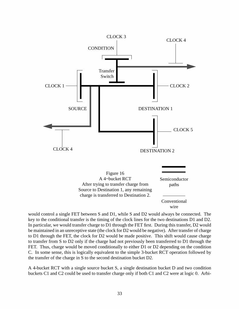
33
would control a single FET between S and D1, while S and D2 would always be connected. Thekey to the conditional transfer is the timing of the clock lines for the two destinations D1 and D2.In particular, we would transfer charge to D1 through the FET first. During this transfer, D2 wouldbe maintained in an unreceptive state (the clock for D2 would be negative). After transfer of chargeto D1 through the FET, the clock for D2 would be made positive. This shift would cause chargeto transfer from S to D2 only if the charge had not previously been transferred to D1 through theFET. Thus, charge would be moved conditionally to either D1 or D2 depending on the conditionC. In some sense, this is logically equivalent to the simple 3-bucket RCT operation followed bythe transfer of the charge in S to the second destination bucket D2.
A 4-bucket RCT with a single source bucket S, a single destination bucket D and two conditionbuckets C1 and C2 could be used to transfer charge only if both C1 and C2 were at logic 0. Arbi-
Figure 16A 4−bucket RCT
After trying to transfer charge fromSource to Destination 1, any remainingcharge is transferred to Destination 2.
CLOCK 1 CLOCK 2
CLOCK 3CLOCK 4
CLOCK 4
SOURCE DESTINATION 1
CONDITION
Semiconductorpaths
Conventionalwire
Transfer Switch
DESTINATION 2
CLOCK 5

34
trary switching functions could be imposed between the source and destination buckets, and thenumber of condition buckets could be increased arbitrarily.
It should be clear that a myriad variations on this theme are possible.
A Planar Version of RCT Logic
It would be advantageous to have a planar layout for an RCT that used only sine waves for clock-ing. This would be easy to implement in current planar technology, and the clock signals could begenerated by LC oscillators. These constraints can be met. In particular, we start by consideringa 3-phase CCD as illustrated in figure 16. The three clocks, Φ0, Φ120 and Φ240, represent three sine
waves offset by 0, 120, and 240 degrees respectively. Charge packets will move from left to rightas the three clock signals vary sinusoidally over time. The illustration shows a top view, the blacksquares being the metalization regions. The metalization typically would be on top of SiO2, withthe bulk Si beneath that. A profile view of charge transfer is given in figure 10.
To provide a switching operation, we must provide some sort of choice for the charge packets mov-ing along the CCD. This is illustrated in figure 18, where the source CCD shift register divides intotwo offspring. To control the direction in which the charge packets are moved, we assume that two“condition” CCD shift registers provide the needed condition packets that will cause charge to se-lect one offspring shift register over the other. Note that this device is just a 5−bucket RCT with asomewhat different geometry and clocking sequence. It uses 3−phase sine wave clocks to movecharge through the device. An additional fourth phase (Φ180) is required to control the conditionalcharge transfer from the single large source well (the large rectangle in the figure) to the two des-tination wells directly to its right.
In this particular planar RCT, Condition1 and Condition2 are two CCD shift registers which holdcomplementary charges. If a potential well in the Condition1 shift register contains a charge pack-et, then the corresponding potential well in the Condition2 shift register does not (and vice versa).The condition charge packet moves from left to right. When it reaches the well clocked by Φ180,the presence or absence of the charge packet changes the voltage on the corresponding gate elec-trode. There are two gate electrodes controlled by the two complementary charge packets. The
Figure 17A 3-phase CCD
Φ0 Φ120 Φ240 Φ0 Φ120 Φ240 Φ0 Φ120 Φ240
Metalization
Direction of packet motion
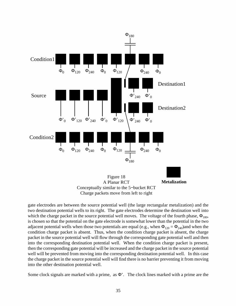
35
gate electrodes are between the source potential well (the large rectangular metalization) and thetwo destination potential wells to its right. The gate electrodes determine the destination well intowhich the charge packet in the source potential well moves. The voltage of the fourth phase, Φ180,is chosen so that the potential on the gate electrode is somewhat lower than the potential in the twoadjacent potential wells when those two potentials are equal (e.g., when Φ120 = Φ240)and when thecondition charge packet is absent. Thus, when the condition charge packet is absent, the chargepacket in the source potential well will flow through the corresponding gate potential well and theninto the corresponding destination potential well. When the condition charge packet is present,then the corresponding gate potential will be increased and the charge packet in the source potentialwell will be prevented from moving into the corresponding destination potential well. In this casethe charge packet in the source potential well will find there is no barrier preventing it from movinginto the other destination potential well.
Some clock signals are marked with a prime, as Φ’. The clock lines marked with a prime are the
Figure 18A Planar RCT
Conceptually similar to the 5−bucket RCTCharge packets move from left to right
Φ0 Φ120 Φ240 Φ0 Φ120 Φ240 Φ0
Φ0 Φ120 Φ240 Φ0 Φ120 Φ240 Φ0
Φ’0 Φ’120 Φ’240 Φ’0 Φ’120 Φ’240 Φ’0
Φ’240 Φ’0
Φ180
Metalization
Φ180
Condition2
Condition1
Source
Destination2
Destination1

36
same as the those that are not so marked except for their DC bias level. Because the condition shiftregisters and the source/destination shift registers share the metalization for the Φ180 clock, andbecause basically different things must occur when a charge packet passes beneath the Φ180 met-alization in the two cases, the DC bias levels for the two sets of clock signals need to be separatelyadjustable. Otherwise, when the gate electrode blocked a charge packet from moving from thesource to the unselected destination, the same voltages applied to the metalizations on the corre-sponding condition shift register would likewise prevent the condition charge packet from movingalong the condition shift register: this, of course, would cause problems. By adjusting the DC biason the condition register clocks, we can insure that condition charge packets will move from leftto right in a regular manner regardless of the voltage variation on the Φ180 clock caused by thepresence or absence of the condition charge packet. In the same way, by adjusting the bias on thesource/destination clocks, we can insure that the voltage variation on the gate electrodes will pre-vent charge packets from moving into the wrong destination, thus insuring reliable switching ac-tion.
In a real circuit, many RCT devices would be interconnected by a complex pattern of CCD shiftregisters. In most cases, this will force the data in one CCD shift register to cross over other shiftregisters. The use of a planar geometry makes the design of such a cross-over nonobvious. A rel-atively simple approach would be to use two crossing sets of metalizations which define two CCDshift registers, and then apply a bias voltage to inactivate one of the shift registers. A charge packetwould be carried along the active shift register and would not be diverted into the inactive shift reg-ister because the bias voltage applied to the inactive shift register would eliminate the potentialwells into which the charge packet might fall. By alternately inactivating one or the other shift reg-ister, charge packets could be carried across in first one and then the other direction. This can belikened to a traffic crossing with a traffic light, where two cars approaching at right angles cannotsimultaneously occupy the intersection. The traffic light is first green in one direction, allowingone car to cross; and is then green in the other direction, allowing the other car to cross.
To summarize this planar RCT: a charge packet moving along a CCD shift register will be movedinto one of two “offspring” or “descendant” shift registers. Which descendant is selected will de-pend on which of two condition shift registers is occupied by a charge packet. This operation islogically universal: it can be used to implement a Fredkin gate and therefore any reversible logiccircuit. Just as this planar RCT is conceptually similar to a 5−bucket RCT, so too a planar versionsimilar to the 4−bucket RCT would also be feasible and would have the practical advantage thatonly a single condition would be required to operate it. The planar 5−bucket RCT suggested hereis intended to show that planar RCT’s using simple sine waves for clocking are feasible. The de-sign of an actual device might well differ significantly.
Conclusions
The historical trend in computer systems is to pack ever more logic gates into ever smaller vol-umes. This trend can only be continued if the energy dissipation per logic operation also continuesto decline. The potential packing densities that nanoelectronic and molecular logic devices shouldbe able to achieve will only be realized if the energy dissipated per logic operation can be reducedto extremely small values. Projections of current trends in energy dissipation per gate operation[6]suggest that the kT “barrier” will become significant within ten to twenty years. This barrier can

37
be overcome by using reversible logic. Reversible logic will be valuable well before the kT barrieris reached. Even though not inherently required when the energy dissipation per logic operation isgreater than kT, reversible designs can more easily reduce energy dissipation than irreversible de-signs even when the actual energy dissipation is orders of magnitude greater than kT. Two methodsof electronic reversible logic using simple electronically controlled switches and capacitors werediscussed. Both approaches can use FET−type switches in their operation. A planar implementa-tion of the CCD based approach using simple sine waves for clocking should be particularly effec-tive in achieving low energy dissipation per logic operation. Breaking the kT barrier is feasible inprinciple, and will eventually be necessary if we are to continue the dramatic improvements incomputer hardware performance and packing densities that we have seen during the last severaldecades. The ultimate limit for electronic devices will be reached when we are able to fabricateatomically precise logic elements that are thermodynamically reversible and use single electronsto represent information. This is likely to occur sometime early in the 21st century.
Acknowledgements
The author would like to thank Bill Athas, Jim Burr, Tord Claeson, Eric Drexler, Edward Fredkin,Mike Hack, Jeff Koller, Rolf Landauer, Alan Lewis, Norman Margolus, Jim Mikkelsen, JohnNorthrup, J. Storrs Hall, Bohumil Polata, Ed Richley, John Shaw, Jeff Soreff, Tommaso Toffoli,Bill Turner and Chris van de Walle.
References
1.) High−Speed Semiconductor Devices, by S. M. Sze, Wiley Interscience 1990.
2.) Rod Logic and Thermal Noise in the Mechanical Nanocomputer, by K. Eric Drexler, in Pro-ceedings of the 3rd International Symposium on Molecular Electronic Devices, F.L. Carter, R.E.Siatkowski, H. Wohltjen, eds., North−Holland 1988.
3.) The Fundamental Physical Limits of Computation, by Charles H. Bennett and Rolf Landau-er, Scientific American, July 1985, pages 48−56.
4.) Single Electronics, by Konstantin K. Likharev and Tord Claeson, Scientific American Vol266 No. 6, June 1992, pages 80−85.
5.) The Fundamentals of Physics, Extended Third Edition, by David Halliday and RobertResnick, Wiley 1988.
6.) Dissipation and noise immunity in computation and communication, by Rolf Landauer, Na-ture, Vol. 335, October 27 1988, page 779.
7.) Conservative Logic, by Edward Fredkin and Tommaso Toffoli, International Journal of The-oretical Physics, Vol. 21, Nos. 3/4, 1982, pages 219−253.
8.) The Thermodynamics of Computation − A Review, by Charles H. Bennett, International Jour-nal of Theoretical Physics, Vol. 21, No. 12, 1982, pages 905−940.
38
9.) Classical and Quantum Limitations on Energy Consumption in Computation, by K. K.Likharev, International Journal of Theoretical Physics, Vol. 21, Nos 3/4, 1982, pages 311 to 326.
10.) Reversible Conveyer Computation in Array of Parametric Quantrons, by K. K. Likharev, S.V. Rylov, and M. K. Semenov, IEEE Transactions on Magnetics, Vol. MAG−21, No. 2, March1985, pages 947−950.
11.) Notes on the History of Reversible Computation, by Charles H. Bennett, IBM J. Researchand Development, Vol. 32, No. 1, January 1988, pages 16− 23.
12.) Engines of Creation, by K. Eric Drexler, Doubleday, 1986.
13.) There’s Plenty of Room at the Bottom, a talk by Richard Feynman (awarded the Nobel Prizein Physics in 1965) at an annual meeting of the American Physical Society given on December 29,1959. Reprinted in “Miniaturization”, edited by H. D. Gilbert (Reinhold, New York, 1961) pages282−296.
14.) A Small Revolution Gets Under Way, by Robert Pool, Science, Jan. 5 1990.
15.) Time/Space Trade−offs for Reversible Computation, by Charles H. Bennett, SIAM J. Com-puting, Vol. 18, No. 4, pages 766−776, August 1989.
16.) Two Types Of Mechanical Reversible Logic, by Ralph C. Merkle, submitted to Nanotechnol-ogy.
18.) Nanosystems: Molecular Machinery, Manufacturing, and Computation, by K. Eric Drexler,John Wiley, 1992.
19.) The Design of a Conservative Logic Computer and a Graphical Editor Simulator, by An-drew Lewis Ressler, Master’s Thesis, Department of Electrical Engineering and Computer Sci-ence, Massachusetts Institute of Technology, January 1981.
20.) Donor Impurities, N−type Doping, and Impurity Diffusion in Diamond, by J. Bernholc, S. A.Kajihara, and A. Antonelli, 20th International Conference on Semiconductors, Volume 1, page332−335.
21.) An Electroid Switching Model for Reversible Computer Architectures, by J. Storrs Hall, Lab-oratory for Computer Science Research, Rutgers University; presented at the Physics of Computa-tion Workshop, Dallas Texas, Oct 2-4 1992.
22.) Quantum photoyield of diamond (111) −−− A Stable negative−affinity emitter, by F. J.Himpsel, J.A. Knapp, J.A. Van Vechten, and D. E. Eastman, Phys. Rev. B, Vol. 20 No. 2, pages624−627.
23.) Design Principles for Achieving High−Performance Submicron Digital Technologies, byEdward Fredkin and Tommaso Toffoli, November 1978 DARPA proposal.
24.) Magnetic Bubbles, by Andrew H. Bobeck and H.E.D. Scovil, Scientific American, June
39
1971, Vol. 224, No. 6, pages 78−91.
25.) Ideal MOS Curves for Silicon, by A. Goetzberger, Bell Systems Technical Journal, Vol 45,September 1966, pages 1097−1122
26.) Single atoms as transistors, by Sean Washburn, Nature Vol 357, May 21 1992, pages 199−200.
27.) A CCD/CMOS process for integrated image acquistion and early vision signal processing,by Craig L. Keast and Charles G. Sodini, SPIE Vol. 1242 Charge−Coupled Devices and Solid StateOptical Sensors (1990), pages 152−161.
28.) Eliminating Threshold Losses in MOS Circuits by Bootstrapping Using Varactor Coupling,by Reuben E Joynson, Joseph L. Mundy, and Constantine Neugebauer, IEEE Journal of Solid−State Circuits, Vol SC−7, No. 3, June 1972, pages 217−224.
29.) Hot−Clock nMOS, by Charles L. Seitz, Alexander H. Frey, Sven Mattisson, Steve D. Rabin,Don A. Speck, Jan L.A. van de Sneepscheut, 1985 Chapel Hill Conference on VLSI, ComputerScience Press, pages 1−17.
30.) Semiconductor Surface Varactor by R. Lindner, The Bell System Technical Journal, Vol. 41No. 3, May 1962, pages 803−831.
31.) Energy−Time Trade−Offs in VLSI Computations, by Akhilesh Tyagi, pages 301−311; inLecture Notes in Computer Science, 1989, Volume 405: Foundations of Software Technology andTheoretical Computer Science, Ninth Conference, Bangalore India, edited by C. E. VeniMadhaven, December 1989.
32.) A Proof about Molecular Bearings, by Ralph C. Merkle, submitted to Nanotechnology.
33.) Private communication, K. Eric Drexler.
34.) Digital Charge-Coupled Logic (DCCL), by T. A. Zimmerman, R. A. Allen, and Robert W.Jacobs, IEEE Journal of Solid State-Circuits, Vol. SC-12, No. 5, October 1977, pages 473-485.
35.) Combinatorial Digital Logic Using Charge−Coupled Devices, by J. Greg Nash, Journal ofSolid−State Circuits, Vol SC−17, No. 5, October 1982, pages 957−963.
36.) Basic C.C.D. Logic Gates, by J. H. Montgomery and H. S. Gamble, The Radio and Electron-ic Engineer, Vol. 50, No. 5., pages 258-268, May 1980.
37.) A New Concept in Computing, by R. L Wigington, Proceedings of the IRE, April 1959, Vol47, No 4, page 516-523.
44.) Approaching the Quantum Limit, by Karl Hess and Gerald J. Iafrate, IEEE Spectrum, Vol.29 No. 7, July 1992, pages 44-49.
45.) Natural Josephson Junctions, by Colin Pegrum, Nature, Vol. 358, July 16 1992, page 193.
40
46.) A Charge-Transfer-Device Logic Cell, by T. D. Mok and C. A. Salama, Solid State Electron-ics 1974, Vol. 17, pages 1147-1154.
47.) Charge Coupled Semiconductor Devices, by W. S. Boyle and G. E. Smith, Bell Sys. Tech.J., Vol. 49, pages 587-593, April 1970.
48.) A Simple Charge Regenerator for Use With Charge-Transfer Devices and the Design ofFunctional Logic Arrays, by Michael F. Tompsett, IEEE Journal of Solid-State Circuits, Vol. SC-7, No. 3, June 1972, pages 237-242.
49.) Bucket−Brigade Electronics − New Possibilities for Delay, Time−Axis Conversion, andScanning, by F.L.J. Sangster and K. Teer, IEEE Journal of Solid−State Circuits, Vol. SC−4, No. 3,June 1969, pages 131−136.
50.) Charge Transfer Devices, by M. F. Tompsett, J. Vac. Sci. Technol., Vol. 9, No. 4, July−Au-gust 1972, pages 1166−1181.
51.) Performance Tests of Large CCD’s, by Lloyed Robinson, William Brown, Kirk Gilmore,Richard Stover, Mingzhi Wei, and John Geary,SPIE Vol. 1447 Charge Coupled Devices and SolidState Optical Sensors II (1991).
52.) The Role of Energy in VLSI Computation, by Akhilesh Tyagi, Ph.D. thesis, University ofWashington, Computer Science, 1988.
53.) CMOS Differential Pass−Transistor Logic Design, by John H. Pasternak, Alex S. Shubat,and C. Andre T. Salama, IEEE Journal of Solid−State Circuits, Vol. SC−22, No. 2, April 1987,pages 216−222.
54.) Two-Dimensional Electron Gas Charge-Coupled Devices (2DEG-CCD’s), by Eric R. Fos-sum, Jong-In Song, and David V. Rossi, IEEE Transactions on Electron Devices, Vol. 38, No. 5,May 1991, pages 1182-1192.
55.) A Unified Theory for MOS circuit design−switching network logic, by Min−You Wu, WeiShu, and Shu−Park Chan, Int. J. Electronics, 1985, Vol. 58 No. 1, pages 1−33.
56.) Boolean Matrices and the Design of Combinational Relay Switching Circuits, by Franz E.Hohn and L. Robert Schissler, Bell System Technical Journal, January 1955, Volume 34, No. 1,pages 177-202.
57.) Introduction to VLSI Systems, by Carver Mead and Lynn Conway, Addison−Wesley 1980.
58.) Diamond Thin−Film Recessed Gate Field−Effect Transistors Fabricated by Electron Cyclo-tron Resonance Plasma Etching, by S. A. Grot, G. Sh. Gildenblat, and A. R. Badzian, IEEE Elec-tron Device Letters, Vol. 13 No. 9, September 1992, pages 462-464.
59.) Low-Power CMOS Digital Design, by Anantha P. Chandrakasan, Samuel Sheng, and RobertW. Brodersen, IEEE Journal of Solid-State Circuits, Vol. 27, No. 4, April 1992, pages 473-484.
41
60.) Course Notes on Program Inversion, by Jan van de Snepscheut, Caltech, 1992, to appear inIntroduction to Computer Science, Spring Verlag, (David Gries’s series) (in preparation).
61.) Adiabiatic Switching, Low Energy Computing, and the Physics of Storing and Erasing In-formation, by Jeffrey G. Koller and William C. Athas, Physics of Computation Workshop, October2-4, Dallas Texas 1992.
62.) Packaging a 150 W Bipolar ECL Microprocessor, by William R. Hamburgen and John S.Fitch, WRL Research Report 92/1, March 1992, Digital Western Research Laboratory, Palo Alto,CA. Also published in 42nd Electronics Components and Technology Conference, Sand Diego,California, May 18-20 1992.
63.) Intel Takes Step To Get Computers To Save Energy, by Rose Gutfield, Wall Street Journal,Thursday October 15, 1992, page B6.
64.) High-performance Heat Sinking for VLSI, by D. B. Tuckerman and R. F. W. Pease, IEEEElectron Device Letters, Vol. EDL-2, No. 5, May 1981, pages 126-129.
65.) Upper and Lower Bounds on Switching Energy in VLSI, by Gloria Kissin, Journal of theACM, Vol. 38, No. 1, January 1991, pages 222-254.
66.) A Symbolic Analysis of Relay and Switching Circuits, by Claude E. Shannon, Transactionsof the American Institute of Electrical Engineers, Volume 57, 1938, pages 713-723.
67.) Helical Logic, by Ralph C. Merkle and K. Eric Drexler, in preparation.
68.) Edward Fredkin, private communication.
69.) Single Charge Tunneling, by H. Grabert and M.H. Devoret (eds), Plenum Press, 1992.