Embed Size (px)
Citation preview

DL150/DRev. 2, May-2001
TVS/Z
ener D
evice
Data
TVS/Zener Device Data
05/01DL150REV 2
DL150/D
ON Semiconductor and are trademarks of Semiconductor Components Industries, LLC (SCILLC). SCILLC reserves the right to make changes without further notice to any products herein. SCILLC makes no warranty, representation or guarantee regarding the suitability of its products for any particular purpose, nor does SCILLC assume any liability arising out of the application or use of any product or circuit, and specifically disclaims any and all liability, including without limitation special, consequential or incidental damages. “Typical” parameters which may be provided in SCILLC data sheets and/or specifications can and do vary in different applications and actual performance may vary over time. All operating parameters, including “Typicals” must be validated for each customer application by customer’s technical experts. SCILLC does not convey any license under its patent rights nor the rights of others. SCILLC products are not designed, intended, or authorized for use as components in systems intended for surgical implant into the body, or other applications intended to support or sustain life, or for any other application in which the failure of the SCILLC product could create a situation where personal injury or death may occur. Should Buyer purchase or use SCILLC products for any such unintended or unauthorized application, Buyer shall indemnify and hold SCILLC and its officers, employees, subsidiaries, affiliates, and distributors harmless against all claims, costs, damages, and expenses, and reasonable attorney fees arising out of, directly or indirectly, any claim of personal injury or death associated with such unintended or unauthorized use, even if such claim alleges that SCILLC was negligent regarding the design or manufacture of the part. SCILLC is an Equal Opportunity/Affirmative Action Employer.
NORTH AMERICA Literature Fulfillment: Literature Distribution Center for ON Semiconductor P.O. Box 5163, Denver, Colorado 80217 USA Phone: 303-675-2175 or 800-344-3860 Toll Free USA/Canada Fax: 303-675-2176 or 800-344-3867 Toll Free USA/Canada Email: [email protected] Fax Response Line: 303-675-2167 or 800-344-3810 Toll Free USA/Canada
N. American Technical Support: 800-282-9855 Toll Free USA/Canada
EUROPE: LDC for ON Semiconductor - European Support German Phone: (+1) 303-308-7140 (Mon-Fri 2:30pm to 7:00pm CET) Email: [email protected] French Phone: (+1) 303-308-7141 (Mon-Fri 2:00pm to 7:00pm CET) Email: [email protected] English Phone: (+1) 303-308-7142 (Mon-Fri 12:00pm to 5:00pm GMT) Email: [email protected]
EUROPEAN TOLL-FREE ACCESS*: 00-800-4422-3781 *Available from Germany, France, Italy, UK, Ireland
CENTRAL/SOUTH AMERICA: Spanish Phone: 303-308-7143 (Mon-Fri 8:00am to 5:00pm MST) Email: [email protected] Toll-Free from Mexico: Dial 01-800-288-2872 for Access - then Dial 866-297-9322
ASIA/PACIFIC: LDC for ON Semiconductor - Asia Support Phone: 303-675-2121 (T-F 9:00am to 1:00pm Hong Kong Time) Toll Free from Hong Kong & Singapore: 001-800-4422-3781 Email: [email protected]
JAPAN: ON Semiconductor, Japan Customer Focus Center 4-32-1 Nishi-Gotanda, Shinagawa-ku, Tokyo, Japan 141-0031 Phone: 81-3-5740-2700 Email: [email protected]
ON Semiconductor Website: http://onsemi.com
PUBLICATION ORDERING INFORMATION
For additional information, please contact your local SalesRepresentative
TVS/Zeners Device Data
Transient Voltage Suppressors and Zener Diodes
DL150/DRev. 2, May–2001
SCILLC, 2001Previous Edition 1994“All Rights Reserved’’

http://onsemi.com2
This book presents technical data for the broad line of ON Semiconductor Transient Voltage Suppressors and Zener Diodes.Complete specifications for the individual devices are provided in the form of data sheets. A comprehensive Selector Guideand Industry Cross Reference Guide are included to simplify the task of choosing the best set of components required for aspecific application. For additional information, please visit our website at: http://onsemi.com
Although information in this book has been carefully checked, no responsibility for inaccuracies can be assumed byON Semiconductor. Please consult your nearest ON Semiconductor sales office for further assistance regarding any aspect ofON Semiconductor products.
ON Semiconductor and are trademarks of Semiconductor Components Industries, LLC (SCILLC). SCILLC reserves the right to make changeswithout further notice to any products herein. SCILLC makes no warranty, representation or guarantee regarding the suitability of its products for any particularpurpose, nor does SCILLC assume any liability arising out of the application or use of any product or circuit, and specifically disclaims any and all liability,including without limitation special, consequential or incidental damages. “Typical” parameters which may be provided in SCILLC data sheets and/orspecifications can and do vary in different applications and actual performance may vary over time. All operating parameters, including “Typicals” must bevalidated for each customer application by customer’s technical experts. SCILLC does not convey any license under its patent rights nor the rights of others.SCILLC products are not designed, intended, or authorized for use as components in systems intended for surgical implant into the body, or other applicationsintended to support or sustain life, or for any other application in which the failure of the SCILLC product could create a situation where personal injury ordeath may occur. Should Buyer purchase or use SCILLC products for any such unintended or unauthorized application, Buyer shall indemnify and holdSCILLC and its officers, employees, subsidiaries, affiliates, and distributors harmless against all claims, costs, damages, and expenses, and reasonableattorney fees arising out of, directly or indirectly, any claim of personal injury or death associated with such unintended or unauthorized use, even if such claimalleges that SCILLC was negligent regarding the design or manufacture of the part. SCILLC is an Equal Opportunity/Affirmative Action Employer.
PUBLICATION ORDERING INFORMATIONCENTRAL/SOUTH AMERICA:Spanish Phone : 303–308–7143 (Mon–Fri 8:00am to 5:00pm MST)
Email : ONlit–[email protected]–Free from Mexico: Dial 01–800–288–2872 for Access –
then Dial 866–297–9322
ASIA/PACIFIC : LDC for ON Semiconductor – Asia SupportPhone : 1–303–675–2121 (Tue–Fri 9:00am to 1:00pm, Hong Kong Time)
Toll Free from Hong Kong & Singapore:001–800–4422–3781
Email : ONlit–[email protected]
JAPAN : ON Semiconductor, Japan Customer Focus Center4–32–1 Nishi–Gotanda, Shinagawa–ku, Tokyo, Japan 141–0031Phone : 81–3–5740–2700Email : [email protected]
ON Semiconductor Website : http://onsemi.com
For additional information, please contact your localSales Representative.
NORTH AMERICA Literature Fulfillment :Literature Distribution Center for ON SemiconductorP.O. Box 5163, Denver, Colorado 80217 USAPhone : 303–675–2175 or 800–344–3860 Toll Free USA/CanadaFax: 303–675–2176 or 800–344–3867 Toll Free USA/CanadaEmail : [email protected] Response Line: 303–675–2167 or 800–344–3810 Toll Free USA/Canada
N. American Technical Support : 800–282–9855 Toll Free USA/Canada
EUROPE: LDC for ON Semiconductor – European SupportGerman Phone : (+1) 303–308–7140 (Mon–Fri 2:30pm to 7:00pm CET)
Email : ONlit–[email protected] Phone : (+1) 303–308–7141 (Mon–Fri 2:00pm to 7:00pm CET)
Email : ONlit–[email protected] Phone : (+1) 303–308–7142 (Mon–Fri 12:00pm to 5:00pm GMT)
Email : [email protected]
EUROPEAN TOLL–FREE ACCESS*: 00–800–4422–3781*Available from Germany, France, Italy, UK, Ireland

http://onsemi.com3
ON SEMICONDUCTOR DEVICE CLASSIFICATIONS
In an effort to provide up–to–date information to the customer regarding the status of any given device, ON Semiconductorhas classified all devices into three categories: Preferred devices, Current products and Not Recommended for New Designproducts.
A Preferred type is a device which is recommended as a first choice for future use. These devices are “preferred” by virtueof their performance, price, functionality, or combination of attributes which offer the overall “best” value to the customer. Thiscategory contains both advanced and mature devices which will remain available for the foreseeable future.
“Preferred devices” are denoted below the device part numbers on the individual data sheets.
Device types identified as “current” may not be a first choice for new designs, but will continue to be available because ofthe popularity and/or standardization or volume usage in current production designs. These products can be acceptable for newdesigns but the preferred types are considered better alternatives for long term usage.
Any device that has not been identified as a “preferred device” is a “current” device.
This data book does not contain any “Not Recommended for New Design” devices.
Surmetic and MOSORB are trademarks of Semiconductor Components Industries, LLC (SCILLC).
Thermal Clad is a trademark of the Bergquist Company.
All brand names and product names appearing in this document are registered trademarks or trademarks of their respectiveholders.
http://onsemi.com4
Table of Contents
PageChapter 1: Alphanumeric Index of Part Numbers 5. . . .
Chapter 2: Selector Guide for TransientVoltage Suppressors and Zener Diodes 13. . . . . . . . . .
Chapter 3: Transient Voltage Suppressors –Axial Leaded Data Sheets 43. . . . . . . . . . . . . . . . . . . . . . .
P6KE6.8A Series 45. . . . . . . . . . . . . . . . . . . . . . . . . . . . . . P6KE6.8CA Series 51. . . . . . . . . . . . . . . . . . . . . . . . . . . . . 1N6267A Series 57. . . . . . . . . . . . . . . . . . . . . . . . . . . . . . . SA5.0A Series 63. . . . . . . . . . . . . . . . . . . . . . . . . . . . . . . . SA5.0CA Series 68. . . . . . . . . . . . . . . . . . . . . . . . . . . . . . . 1.5KE6.8CA Series 72. . . . . . . . . . . . . . . . . . . . . . . . . . . . 1N5908 78. . . . . . . . . . . . . . . . . . . . . . . . . . . . . . . . . . . . . . 1N6373 Series 83. . . . . . . . . . . . . . . . . . . . . . . . . . . . . . . . 1N6382 Series 88. . . . . . . . . . . . . . . . . . . . . . . . . . . . . . . .
Chapter 4: Transient Voltage Suppressors –Surface Mounted Data Sheets 93. . . . . . . . . . . . . . . . . . .
1PMT5.0AT3 Series 94. . . . . . . . . . . . . . . . . . . . . . . . . . . . 1SMA5.0AT3 Series 98. . . . . . . . . . . . . . . . . . . . . . . . . . . . 1SMA10CAT3 Series 102. . . . . . . . . . . . . . . . . . . . . . . . . . 1SMB5.0AT3 Series 105. . . . . . . . . . . . . . . . . . . . . . . . . . . P6SMB6.8AT3 Series 111. . . . . . . . . . . . . . . . . . . . . . . . . 1SMB10CAT3 Series 117. . . . . . . . . . . . . . . . . . . . . . . . . . P6SMB11CAT3 Series 122. . . . . . . . . . . . . . . . . . . . . . . . 1SMC5.0AT3 Series 127. . . . . . . . . . . . . . . . . . . . . . . . . . 1.5SMC6.8AT3 Series 133. . . . . . . . . . . . . . . . . . . . . . . . .
Chapter 5: Transient Voltage Suppressor Arrays –Surface Mounted Data Sheets 139. . . . . . . . . . . . . . . . . .
MMBZ5V6ALT1 Series 140. . . . . . . . . . . . . . . . . . . . . . . . MMBZ15VDLT1, MMBZ27VCLT1 146. . . . . . . . . . . . . . . MMQA5V6T1 Series 150. . . . . . . . . . . . . . . . . . . . . . . . . . MSQA6V1W5T2 155. . . . . . . . . . . . . . . . . . . . . . . . . . . . . . DF6A6.8FUT1 158. . . . . . . . . . . . . . . . . . . . . . . . . . . . . . . . SMS05T1 160. . . . . . . . . . . . . . . . . . . . . . . . . . . . . . . . . . . .
Chapter 6: Zener Voltage Regulator Diodes –Axial Leaded Data Sheets 163. . . . . . . . . . . . . . . . . . . . . .
1N4370A Series 165. . . . . . . . . . . . . . . . . . . . . . . . . . . . . . 1N957B Series 173. . . . . . . . . . . . . . . . . . . . . . . . . . . . . . . 1N5985B Series 181. . . . . . . . . . . . . . . . . . . . . . . . . . . . . . BZX79C2V4RL Series 189. . . . . . . . . . . . . . . . . . . . . . . . . 1N4678 Series 197. . . . . . . . . . . . . . . . . . . . . . . . . . . . . . . 1N5221B Series 206. . . . . . . . . . . . . . . . . . . . . . . . . . . . . . 1N4728A Series 215. . . . . . . . . . . . . . . . . . . . . . . . . . . . . . BZX85C3V3RL Series 221. . . . . . . . . . . . . . . . . . . . . . . . . 1N5913B Series 228. . . . . . . . . . . . . . . . . . . . . . . . . . . . . . 3EZ4.3D5 Series 234. . . . . . . . . . . . . . . . . . . . . . . . . . . . . MZP4729A Series 240. . . . . . . . . . . . . . . . . . . . . . . . . . . . 1N5333B Series 246. . . . . . . . . . . . . . . . . . . . . . . . . . . . . .
PageChapter 7: Zener Voltage Regulator Diodes –Surface Mounted Data Sheets 253. . . . . . . . . . . . . . . . . .
MM3Z2V4T1 Series 254. . . . . . . . . . . . . . . . . . . . . . . . . . . BZX84C2V4LT1 Series 259. . . . . . . . . . . . . . . . . . . . . . . . MMBZ5221BLT1 Series 264. . . . . . . . . . . . . . . . . . . . . . . MMSZ5221BT1 Series 269. . . . . . . . . . . . . . . . . . . . . . . . MMSZ4678T1 Series 274. . . . . . . . . . . . . . . . . . . . . . . . . . MMSZ2V4T1 Series 279. . . . . . . . . . . . . . . . . . . . . . . . . . . 1PMT5920BT3 Series 283. . . . . . . . . . . . . . . . . . . . . . . . . 1SMA5913BT3 Series 287. . . . . . . . . . . . . . . . . . . . . . . . . 1SMB5913BT3 Series 292. . . . . . . . . . . . . . . . . . . . . . . . .
Chapter 8: Surface Mount Information andPackaging Specifications 297. . . . . . . . . . . . . . . . . . . . . .
Footprints for Soldering 302. . . . . . . . . . . . . . . . . . . . . . . .
Chapter 9: Package Outline Dimensions 311. . . . . . . . .
Chapter 10: Technical Information,Application Notes and Articles 321. . . . . . . . . . . . . . . . . .
Zener Diode Theory 323. . . . . . . . . . . . . . . . . . . . . . . . . . . Zener Diode Fabrication Techniques 328. . . . . . . . . . . . . Reliability 332. . . . . . . . . . . . . . . . . . . . . . . . . . . . . . . . . . . . Zener Diode Characteristics 338. . . . . . . . . . . . . . . . . . . . Temperature Compensated Zeners 350. . . . . . . . . . . . . . Basic Voltage Regulation Using Zener Diodes 354. . . . Zener Protective Circuits and Techniques:
Basic Design Considerations 364. . . . . . . . . . . . . . . . Zener Voltage Sensing Circuits and Applications 374. . Miscellaneous Applications of
Zener Type Devices 381. . . . . . . . . . . . . . . . . . . . . . . . Transient Voltage Suppression 383. . . . . . . . . . . . . . . . . AN784 402. . . . . . . . . . . . . . . . . . . . . . . . . . . . . . . . . . . . . . AN843 404. . . . . . . . . . . . . . . . . . . . . . . . . . . . . . . . . . . . . . Design Considerations and Performance of
Temperature Compensated Zener Diodes 417. . . . . MOSORBs 422. . . . . . . . . . . . . . . . . . . . . . . . . . . . . . . . . . . AR450 426. . . . . . . . . . . . . . . . . . . . . . . . . . . . . . . . . . . . . . Measurement of Zener Voltage to Thermal
Equilibrium with Pulsed Test Current 439. . . . . . . . . . Sales Office List 447. . . . . . . . . . . . . . . . . . . . . . . . . . . . . . Standard Document Type Definitions 448. . . . . . . . . . . .

http://onsemi.com5
CHAPTER 1Alphanumeric Index of Part Numbers

http://onsemi.com6
DEVICE PAGE
1.5KE100A 59
1.5KE100CA 74
1.5KE10A 59
1.5KE10CA 74
1.5KE110A 59
1.5KE110CA 74
1.5KE11A 59
1.5KE11CA 74
1.5KE120A 59
1.5KE120CA 74
1.5KE12A 59
1.5KE12CA 74
1.5KE130A 59
1.5KE130CA 74
1.5KE13A 59
1.5KE13CA 74
1.5KE150A 59
1.5KE150CA 74
1.5KE15A 59
1.5KE15CA 74
1.5KE160A 59
1.5KE160CA 74
1.5KE16A 59
1.5KE16CA 74
1.5KE170A 59
1.5KE170CA 74
1.5KE180A 59
1.5KE180CA 74
1.5KE18A 59
1.5KE18CA 74
1.5KE200A 59
1.5KE200CA 74
1.5KE20A 59
1.5KE20CA 74
1.5KE220A 59
1.5KE220CA 74
1.5KE22A 59
1.5KE22CA 74
1.5KE24A 59
1.5KE24CA 74
1.5KE250A 59
1.5KE250CA 74
1.5KE27A 59
1.5KE27CA 74
1.5KE30A 59
1.5KE30CA 74
DEVICE PAGE
1.5KE33A 59
1.5KE33CA 74
1.5KE36A 59
1.5KE36CA 74
1.5KE39A 59
1.5KE39CA 74
1.5KE43A 59
1.5KE43CA 74
1.5KE47A 59
1.5KE47CA 74
1.5KE51A 59
1.5KE51CA 74
1.5KE56A 59
1.5KE56CA 74
1.5KE6.8A 59
1.5KE6.8CA 74
1.5KE62A 59
1.5KE62CA 74
1.5KE68A 59
1.5KE68CA 74
1.5KE7.5A 59
1.5KE7.5CA 74
1.5KE75A 59
1.5KE75CA 74
1.5KE8.2A 59
1.5KE8.2CA 74
1.5KE82A 59
1.5KE82CA 74
1.5KE9.1A 59
1.5KE9.1CA 74
1.5KE91A 59
1.5KE91CA 74
1.5SMC10AT3 135
1.5SMC11AT3 135
1.5SMC12AT3 135
1.5SMC13AT3 135
1.5SMC15AT3 135
1.5SMC16AT3 135
1.5SMC18AT3 135
1.5SMC20AT3 135
1.5SMC22AT3 135
1.5SMC24AT3 135
1.5SMC27AT3 135
1.5SMC30AT3 135
1.5SMC33AT3 135
1.5SMC36AT3 135
DEVICE PAGE
1.5SMC39AT3 135
1.5SMC43AT3 135
1.5SMC47AT3 135
1.5SMC51AT3 135
1.5SMC56AT3 135
1.5SMC6.8AT3 135
1.5SMC62AT3 135
1.5SMC68AT3 135
1.5SMC7.5AT3 135
1.5SMC75AT3 135
1.5SMC8.2AT3 135
1.5SMC82AT3 135
1.5SMC9.1AT3 135
1.5SMC91AT3 135
1N4370A 166
1N4371A 166
1N4372A 166
1N4678 199
1N4679 199
1N4680 199
1N4681 199
1N4682 199
1N4683 199
1N4684 199
1N4685 199
1N4686 199
1N4687 199
1N4688 199
1N4689 199
1N4690 199
1N4691 199
1N4692 199
1N4693 199
1N4694 199
1N4695 199
1N4696 199
1N4697 199
1N4698 199
1N4699 199
1N4700 199
1N4701 199
1N4702 199
1N4703 199
1N4704 199
1N4705 199
1N4707 199
DEVICE PAGE
1N4711 199
1N4728A 216
1N4729A 216
1N4730A 216
1N4731A 216
1N4732A 216
1N4733A 216
1N4734A 216
1N4735A 216
1N4736A 216
1N4737A 216
1N4738A 216
1N4739A 216
1N4740A 216
1N4741A 216
1N4742A 216
1N4743A 216
1N4744A 216
1N4745A 216
1N4746A 217
1N4747A 217
1N4748A 217
1N4749A 217
1N4750A 217
1N4751A 217
1N4752A 217
1N4753A 217
1N4754A 217
1N4755A 217
1N4756A 217
1N4757A 217
1N4758A 217
1N4759A 217
1N4760A 217
1N4761A 217
1N4762A 217
1N4763A 217
1N5221B 207
1N5222B 207
1N5223B 207
1N5224B 207
1N5225B 207
1N5226B 207
1N5227B 207
1N5228B 207
1N5229B 207

http://onsemi.com7
DEVICE PAGE
1N5230B 207
1N5231B 207
1N5232B 207
1N5233B 207
1N5234B 207
1N5235B 207
1N5236B 208
1N5237B 208
1N5238B 208
1N5239B 208
1N5240B 208
1N5241B 208
1N5242B 208
1N5243B 208
1N5244B 208
1N5245B 208
1N5246B 208
1N5247B 208
1N5248B 208
1N5249B 208
1N5250B 208
1N5251B 208
1N5252B 208
1N5253B 208
1N5254B 208
1N5255B 208
1N5256B 208
1N5257B 208
1N5258B 208
1N5259B 208
1N5260B 208
1N5261B 208
1N5262B 208
1N5263B 208
1N5264B 208
1N5265B 208
1N5266B 208
1N5267B 208
1N5268B 208
1N5269B 208
1N5270B 208
1N5333B 248
1N5334B 248
1N5335B 248
1N5336B 248
1N5337B 248
DEVICE PAGE
1N5338B 248
1N5339B 248
1N5340B 248
1N5341B 248
1N5342B 248
1N5343B 248
1N5344B 248
1N5345B 248
1N5346B 248
1N5347B 248
1N5348B 248
1N5349B 248
1N5350B 248
1N5351B 248
1N5352B 248
1N5353B 248
1N5354B 248
1N5355B 248
1N5356B 248
1N5357B 248
1N5358B 248
1N5359B 248
1N5360B 248
1N5361B 248
1N5362B 248
1N5363B 249
1N5364B 249
1N5365B 249
1N5366B 249
1N5367B 249
1N5368B 249
1N5369B 249
1N5370B 249
1N5371B 249
1N5372B 249
1N5373B 249
1N5374B 249
1N5375B 249
1N5376B 249
1N5377B 249
1N5378B 249
1N5379B 249
1N5380B 249
1N5381B 249
1N5382B 249
1N5383B 249
DEVICE PAGE
1N5384B 249
1N5385B 249
1N5386B 249
1N5387B 249
1N5388B 249
1N5908 78
1N5913B 230
1N5917B 230
1N5919B 230
1N5920B 230
1N5921B 230
1N5923B 230
1N5924B 230
1N5925B 230
1N5926B 230
1N5927B 230
1N5929B 230
1N5930B 230
1N5931B 230
1N5932B 230
1N5933B 230
1N5934B 230
1N5935B 230
1N5936B 230
1N5937B 230
1N5938B 230
1N5940B 230
1N5941B 230
1N5942B 230
1N5943B 230
1N5944B 230
1N5945B 230
1N5946B 230
1N5947B 230
1N5948B 230
1N5950B 230
1N5951B 230
1N5952B 230
1N5953B 230
1N5954B 230
1N5955B 230
1N5956B 230
1N5985B 182
1N5987B 182
1N5988B 182
1N5990B 182
DEVICE PAGE
1N5991B 182
1N5992B 182
1N5993B 182
1N5994B 182
1N5995B 182
1N5996B 182
1N5997B 182
1N5998B 182
1N5999B 182
1N6000B 182
1N6001B 182
1N6002B 182
1N6004B 182
1N6007B 182
1N6373 84
1N6374 84
1N6375 84
1N6376 84
1N6377 84
1N6378 84
1N6379 84
1N6380 84
1N6381 84
1N6382 89
1N6383 89
1N6384 89
1N6385 89
1N6386 89
1N6387 89
1N6388 89
1N6389 89
1N746A 166
1N747A 166
1N748A 166
1N749A 166
1N750A 166
1N751A 166
1N752A 166
1N753A 166
1N754A 166
1N755A 166
1N756A 166
1N757A 166
1N758A 166
1N759A 166
1N957B 174

http://onsemi.com8
DEVICE PAGE
1N958B 174
1N959B 174
1N960B 174
1N961B 174
1N962B 174
1N963B 174
1N964B 174
1N965B 174
1N966B 174
1N967B 174
1N968B 174
1N969B 174
1N970B 174
1N971B 174
1N972B 174
1N973B 174
1N974B 174
1N975B 174
1N978B 174
1N979B 174
1N982B 174
1PMT12AT3 95
1PMT16AT3 95
1PMT18AT3 95
1PMT22AT3 95
1PMT24AT3 95
1PMT26AT3 95
1PMT28AT3 95
1PMT30AT3 95
1PMT33AT3 95
1PMT36AT3 95
1PMT40AT3 95
1PMT48AT3 95
1PMT5.0AT3 95
1PMT51AT3 95
1PMT58AT3 95
1PMT5920BT3 284
1PMT5219BT3 284
1PMT5922BT3 284
1PMT5923BT3 284
1PMT5924BT3 284
1PMT5925BT3 284
1PMT5927BT3 284
1PMT5929BT3 284
1PMT5930BT3 284
1PMT5931BT3 284
DEVICE PAGE
1PMT5933BT3 284
1PMT5934BT3 284
1PMT5935BT3 284
1PMT5936BT3 284
1PMT5939BT3 284
1PMT7.0AT3 284
1PMT59BT3 95
1SMA10AT3 100
1SMA10CAT3 103
1SMA11AT3 100
1SMA11CAT3 103
1SMA12AT3 100
1SMA12CAT3 103
1SMA13AT3 100
1SMA13CAT3 103
1SMA14AT3 100
1SMA14CAT3 103
1SMA15AT3 100
1SMA15CAT3 103
1SMA16AT3 100
1SMA16CAT3 103
1SMA17AT3 100
1SMA17CAT3 103
1SMA18AT3 100
1SMA18CAT3 103
1SMA20AT3 100
1SMA20CAT3 103
1SMA22AT3 100
1SMA22CAT3 103
1SMA24AT3 100
1SMA24CAT3 103
1SMA26AT3 100
1SMA26CAT3 103
1SMA28AT3 100
1SMA28CAT3 103
1SMA30AT3 100
1SMA30CAT3 103
1SMA33AT3 100
1SMA33CAT3 103
1SMA36AT3 100
1SMA36CAT3 103
1SMA40AT3 100
1SMA40CAT3 103
1SMA43AT3 100
1SMA43CAT3 103
1SMA45AT3 100
DEVICE PAGE
1SMA45CAT3 103
1SMA48AT3 100
1SMA48CAT3 103
1SMA5.0AT3 100
1SMA51AT3 100
1SMA51CAT3 103
1SMA54AT3 100
1SMA54CAT3 103
1SMA58AT3 100
1SMA58CAT3 103
1SMA5913BT3 289
1SMA5914BT3 289
1SMA5915BT3 289
1SMA5916BT3 289
1SMA5917BT3 289
1SMA5918BT3 289
1SMA5919BT3 289
1SMA5920BT3 289
1SMA5921BT3 289
1SMA5922BT3 289
1SMA5923BT3 289
1SMA5924BT3 289
1SMA5925BT3 289
1SMA5926BT3 289
1SMA5927BT3 289
1SMA5928BT3 289
1SMA5929BT3 289
1SMA5930BT3 289
1SMA5931BT3 289
1SMA5932BT3 289
1SMA5933BT3 289
1SMA5934BT3 289
1SMA5935BT3 289
1SMA5936BT3 289
1SMA5937BT3 289
1SMA5938BT3 289
1SMA5939BT3 289
1SMA5940BT3 289
1SMA5941BT3 289
1SMA5942BT3 289
1SMA5943BT3 289
1SMA5944BT3 289
1SMA5945BT3 289
1SMA6.0AT3 100
1SMA6.5AT3 100
1SMA60AT3 100
DEVICE PAGE
1SMA60CAT3 103
1SMA64AT3 100
1SMA64CAT3 103
1SMA7.0AT3 100
1SMA7.5AT3 100
1SMA70AT3 100
1SMA70CAT3 103
1SMA75AT3 100
1SMA75CAT3 103
1SMA78AT3 100
1SMA78CAT3 103
1SMA8.0AT3 100
1SMA8.5AT3 100
1SMA9.0AT3 100
1SMB100AT3 107
1SMB10AT3 107
1SMB10CAT3 118
1SMB110AT3 107
1SMB11AT3 107
1SMB11CAT3 118
1SMB120AT3 107
1SMB12AT3 107
1SMB12CAT3 118
1SMB130AT3 107
1SMB13AT3 107
1SMB13CAT3 118
1SMB14AT3 107
1SMB14CAT3 118
1SMB150AT3 107
1SMB15AT3 107
1SMB15CAT3 118
1SMB160AT3 107
1SMB16AT3 107
1SMB16CAT3 118
1SMB170AT3 107
1SMB17AT3 107
1SMB17CAT3 118
1SMB18AT3 107
1SMB18CAT3 118
1SMB20AT3 107
1SMB20CAT3 118
1SMB22AT3 107
1SMB22CAT3 118
1SMB24AT3 107
1SMB24CAT3 118
1SMB26AT3 107

http://onsemi.com9
DEVICE PAGE
1SMB26CAT3 118
1SMB28AT3 107
1SMB28CAT3 118
1SMB30AT3 107
1SMB30CAT3 118
1SMB33AT3 107
1SMB33CAT3 118
1SMB36AT3 107
1SMB36CAT3 118
1SMB40AT3 107
1SMB40CAT3 118
1SMB43AT3 107
1SMB43CAT3 118
1SMB45AT3 107
1SMB45CAT3 118
1SMB48AT3 107
1SMB48CAT3 118
1SMB5.0AT3 107
1SMB51AT3 107
1SMB51CAT3 118
1SMB54AT3 107
1SMB54CAT3 118
1SMB58AT3 107
1SMB58CAT3 118
1SMB5913BT3 294
1SMB5914BT3 294
1SMB5915BT3 294
1SMB5916BT3 294
1SMB5917BT3 294
1SMB5918BT3 294
1SMB5919BT3 294
1SMB5920BT3 294
1SMB5921BT3 294
1SMB5922BT3 294
1SMB5923BT3 294
1SMB5924BT3 294
1SMB5925BT3 294
1SMB5926BT3 294
1SMB5927BT3 294
1SMB5928BT3 294
1SMB5929BT3 294
1SMB5930BT3 294
1SMB5931BT3 294
1SMB5932BT3 294
1SMB5933BT3 294
1SMB5934BT3 294
DEVICE PAGE
1SMB5935BT3 294
1SMB5936BT3 294
1SMB5937BT3 294
1SMB5938BT3 294
1SMB5939BT3 294
1SMB5940BT3 294
1SMB5941BT3 294
1SMB5942BT3 294
1SMB5943BT3 294
1SMB5944BT3 294
1SMB5945BT3 294
1SMB5946BT3 294
1SMB5947BT3 294
1SMB5948BT3 294
1SMB5949BT3 294
1SMB5950BT3 294
1SMB5951BT3 294
1SMB5952BT3 294
1SMB5953BT3 294
1SMB5954BT3 294
1SMB5955BT3 294
1SMB5956BT3 294
1SMB6.0AT3 107
1SMB6.5AT3 107
1SMB60AT3 107
1SMB60CAT3 118
1SMB64AT3 107
1SMB64CAT3 118
1SMB7.0AT3 107
1SMB7.5AT3 107
1SMB70AT3 107
1SMB70CAT3 118
1SMB75AT3 107
1SMB75CAT3 118
1SMB78AT3 107
1SMB78CAT3 118
1SMB8.0AT3 107
1SMB8.5AT3 107
1SMB85AT3 107
1SMB9.0AT3 107
1SMB90AT3 107
1SMC10AT3 129
1SMC11AT3 129
1SMC12AT3 129
1SMC13AT3 129
1SMC14AT3 129
DEVICE PAGE
1SMC15AT3 129
1SMC16AT3 129
1SMC17AT3 129
1SMC18AT3 129
1SMC20AT3 129
1SMC22AT3 129
1SMC24AT3 129
1SMC26AT3 129
1SMC28AT3 129
1SMC30AT3 129
1SMC33AT3 129
1SMC36AT3 129
1SMC40AT3 129
1SMC43AT3 129
1SMC45AT3 129
1SMC48AT3 129
1SMC5.0AT3 129
1SMC51AT3 129
1SMC54AT3 129
1SMC58AT3 129
1SMC6.0AT3 129
1SMC6.5AT3 129
1SMC60AT3 129
1SMC64AT3 129
1SMC7.0AT3 129
1SMC7.5AT3 129
1SMC70AT3 129
1SMC75AT3 129
1SMC78AT3 129
1SMC8.0AT3 129
1SMC8.5AT3 129
1SMC9.0AT3 129
3EZ10D5 236
3EZ13D5 236
3EZ15D5 236
3EZ16D5 236
3EZ18D5 236
3EZ220D5 236
3EZ240D5 236
3EZ24D5 236
3EZ330D5 236
3EZ36D5 236
3EZ39D5 236
3EZ4.3D5 236
3EZ6.2D5 236
3EZ8.2D5 236
DEVICE PAGE
BZX79C10RL 190
BZX79C12RL 190
BZX79C15RL 190
BZX79C16RL 190
BZX79C18RL 190
BZX79C22RL 190
BZX79C24RL 190
BZX79C27RL 190
BZX79C2V4RL 190
BZX79C2V7RL 190
BZX79C30RL 190
BZX79C33RL 190
BZX79C3V0RL 190
BZX79C3V3RL 190
BZX79C3V6RL 190
BZX79C3V9RL 190
BZX79C4V7RL 190
BZX79C5V1RL 190
BZX79C5V6RL 190
BZX79C6V2RL 190
BZX79C6V8RL 190
BZX79C7V5RL 190
BZX79C8V2RL 190
BZX84C10LT1 261
BZX84C11LT1 261
BZX84C12LT1 261
BZX84C13LT1 261
BZX84C15LT1 261
BZX84C16LT1 261
BZX84C18LT1 261
BZX84C20LT1 261
BZX84C22LT1 261
BZX84C24LT1 261
BZX84C27LT1 261
BZX84C2V4LT1 261
BZX84C2V7LT1 261
BZX84C30LT1 261
BZX84C33LT1 261
BZX84C36LT1 261
BZX84C39LT1 261
BZX84C3V0LT1 261
BZX84C3V3LT1 261
BZX84C3V6LT1 261
BZX84C3V9LT1 261
BZX84C43LT1 261
BZX84C47LT1 261

http://onsemi.com10
DEVICE PAGE
BZX84C4V3LT1 261
BZX84C4V7LT1 261
BZX84C51LT1 261
BZX84C56LT1 261
BZX84C5V1LT1 261
BZX84C5V6LT1 261
BZX84C62LT1 261
BZX84C68LT1 261
BZX84C6V2LT1 261
BZX84C6V8LT1 261
BZX84C75LT1 261
BZX84C7V5LT1 261
BZX84C8V2LT1 261
BZX84C9V1LT1 261
BZX85C10RL 223
BZX85C12RL 223
BZX85C13RL 223
BZX85C15RL 223
BZX85C16RL 223
BZX85C18RL 223
BZX85C22RL 223
BZX85C24RL 223
BZX85C27RL 223
BZX85C30RL 223
BZX85C33RL 223
BZX85C36RL 223
BZX85C3V3RL 223
BZX85C3V6RL 223
BZX85C3V9RL 223
BZX85C43RL 223
BZX85C47RL 223
BZX85C4V3RL 223
BZX85C4V7RL 223
BZX85C5V1RL 223
BZX85C5V6RL 223
BZX85C62RL 223
BZX85C6V2RL 223
BZX85C6V8RL 223
BZX85C75RL 223
BZX85C7V5RL 223
BZX85C82RL 223
BZX85C8V2RL 223
BZX85C9V1RL 223
DF6A6.8FUT1 158
ICTE–10 84
ICTE–10C 89
DEVICE PAGE
ICTE–12 84
ICTE–12C 89
ICTE–15 84
ICTE–15C 89
ICTE–18 84
ICTE–18C 89
ICTE–22 84
ICTE–22C 89
ICTE–36 84
ICTE–36C 89
ICTE–5 84
MM3Z10VT1 256
MM3Z11VT1 256
MM3Z12VT1 256
MM3Z13VT1 256
MM3Z15VT1 256
MM3Z16VT1 256
MM3Z18VT1 256
MM3Z20VT1 256
MM3Z22VT1 256
MM3Z24VT1 256
MM3Z27VT1 256
MM3Z2V4T1 256
MM3Z2V7T1 256
MM3Z30VT1 256
MM3Z33VT1 256
MM3Z36VT1 256
MM3Z39VT1 256
MM3Z3V0T1 256
MM3Z3V3T1 256
MM3Z3V6T1 256
MM3Z3V9T1 256
MM3Z43VT1 256
MM3Z47VT1 256
MM3Z4V3T1 256
MM3Z4V7T1 256
MM3Z51VT1 256
MM3Z56VT1 256
MM3Z5V1T1 256
MM3Z5V6T1 256
MM3Z62VT1 256
MM3Z68VT1 256
MM3Z6V2T1 256
MM3Z6V8T1 256
MM3Z75VT1 256
MM3Z7V5T1 256
DEVICE PAGE
MM3Z8V2T1 256
MM3Z9V1T1 256
MMBZ10VALT1 140
MMBZ12VALT1 140
MMBZ15VALT1 140
MMBZ15VDLT1 146
MMBZ18VALT1 140
MMBZ20VALT1 140
MMBZ27VALT1 140
MMBZ27VCLT1 146
MMBZ33VALT1 140
MMBZ5221BLT1 266
MMBZ5222BLT1 266
MMBZ5223BLT1 266
MMBZ5224BLT1 266
MMBZ5225BLT1 266
MMBZ5226BLT1 266
MMBZ5227BLT1 266
MMBZ5228BLT1 266
MMBZ5229BLT1 266
MMBZ5230BLT1 266
MMBZ5231BLT1 266
MMBZ5232BLT1 266
MMBZ5233BLT1 266
MMBZ5234BLT1 266
MMBZ5235BLT1 266
MMBZ5236BLT1 266
MMBZ5237BLT1 266
MMBZ5238BLT1 266
MMBZ5239BLT1 266
MMBZ5240BLT1 266
MMBZ5241BLT1 266
MMBZ5242BLT1 266
MMBZ5243BLT1 266
MMBZ5244BLT1 266
MMBZ5245BLT1 266
MMBZ5246BLT1 266
MMBZ5247BLT1 266
MMBZ5248BLT1 266
MMBZ5249BLT1 266
MMBZ5250BLT1 266
MMBZ5251BLT1 266
MMBZ5252BLT1 266
MMBZ5253BLT1 266
MMBZ5254BLT1 266
MMBZ5255BLT1 266
DEVICE PAGE
MMBZ5256BLT1 266
MMBZ5257BLT1 266
MMBZ5258BLT1 266
MMBZ5259BLT1 266
MMBZ5260BLT1 266
MMBZ5261BLT1 266
MMBZ5262BLT1 266
MMBZ5263BLT1 266
MMBZ5264BLT1 266
MMBZ5265BLT1 266
MMBZ5266BLT1 266
MMBZ5267BLT1 266
MMBZ5268BLT1 266
MMBZ5269BLT1 266
MMBZ5270BLT1 266
MMBZ5V6ALT1 140
MMBZ6V2ALT1 140
MMBZ6V8ALT1 140
MMBZ9V1ALT1 140
MMQA12VT1 151
MMQA13VT1 151
MMQA15VT1 151
MMQA18VT1 151
MMQA20VT1 151
MMQA21VT1 151
MMQA22VT1 151
MMQA24VT1 151
MMQA27VT1 151
MMQA30VT1 151
MMQA33VT1 151
MMQA5V6T1 151
MMQA6V2T1 151
MMQA6V8T1 151
MMSZ10T1 280
MMSZ11T1 280
MMSZ12T1 280
MMSZ13T1 280
MMSZ15T1 280
MMSZ16T1 280
MMSZ18T1 280
MMSZ20T1 280
MMSZ22T1 280
MMSZ24T1 280
MMSZ27T1 280
MMSZ2V4T1 280
MMSZ2V7T1 280

http://onsemi.com11
DEVICE PAGE
MMSZ30T1 280
MMSZ33T1 280
MMSZ36T1 280
MMSZ39T1 280
MMSZ3V0T1 280
MMSZ3V3T1 280
MMSZ3V6T1 280
MMSZ3V9T1 280
MMSZ43T1 280
MMSZ4678T1 276
MMSZ4679T1 276
MMSZ4680T1 276
MMSZ4681T1 276
MMSZ4682T1 276
MMSZ4683T1 276
MMSZ4684T1 276
MMSZ4685T1 276
MMSZ4686T1 276
MMSZ4687T1 276
MMSZ4688T1 276
MMSZ4689T1 276
MMSZ4690T1 276
MMSZ4691T1 276
MMSZ4692T1 276
MMSZ4693T1 276
MMSZ4694T1 276
MMSZ4695T1 276
MMSZ4696T1 276
MMSZ4697T1 276
MMSZ4698T1 276
MMSZ4699T1 276
MMSZ4700T1 276
MMSZ4701T1 276
MMSZ4702T1 276
MMSZ4703T1 276
MMSZ4704T1 276
MMSZ4705T1 276
MMSZ4706T1 276
MMSZ4707T1 276
MMSZ4708T1 276
MMSZ4709T1 276
MMSZ4710T1 276
MMSZ4711T1 276
MMSZ4712T1 276
MMSZ4713T1 276
MMSZ4714T1 276
DEVICE PAGE
MMSZ4715T1 276
MMSZ4716T1 276
MMSZ4717T1 276
MMSZ4V3T1 280
MMSZ4V7T1 280
MMSZ51T1 280
MMSZ5221BT1 271
MMSZ5222BT1 271
MMSZ5223BT1 271
MMSZ5224BT1 271
MMSZ5225BT1 271
MMSZ5226BT1 271
MMSZ5227BT1 271
MMSZ5228BT1 271
MMSZ5229BT1 271
MMSZ5230BT1 271
MMSZ5231BT1 271
MMSZ5232BT1 271
MMSZ5233BT1 271
MMSZ5234BT1 271
MMSZ5235BT1 271
MMSZ5236BT1 271
MMSZ5237BT1 271
MMSZ5238BT1 271
MMSZ5239BT1 271
MMSZ5240BT1 271
MMSZ5241BT1 271
MMSZ5242BT1 271
MMSZ5243BT1 271
MMSZ5244BT1 271
MMSZ5245BT1 271
MMSZ5246BT1 271
MMSZ5247BT1 271
MMSZ5248BT1 271
MMSZ5249BT1 271
MMSZ5250BT1 271
MMSZ5251BT1 271
MMSZ5252BT1 271
MMSZ5253BT1 271
MMSZ5254BT1 271
MMSZ5255BT1 271
MMSZ5256BT1 271
MMSZ5257BT1 271
MMSZ5258BT1 271
MMSZ5259BT1 271
MMSZ5260BT1 271
DEVICE PAGE
MMSZ5261BT1 271
MMSZ5262BT1 271
MMSZ5263BT1 271
MMSZ5264BT1 271
MMSZ5265BT1 271
MMSZ5266BT1 271
MMSZ5267BT1 271
MMSZ5268BT1 271
MMSZ5269BT1 271
MMSZ5270BT1 271
MMSZ5272BT1 271
MMSZ56T1 280
MMSZ5V1T1 280
MMSZ5V6T1 280
MMSZ6V2T1 280
MMSZ6V8T1 280
MMSZ7V5T1 280
MMSZ8V2T1 280
MMSZ9V1T1 280
MSQA6V1W5T2 155
MZP4729A 242
MZP4734A 242
MZP4735A 242
MZP4736A 242
MZP4737A 242
MZP4738A 242
MZP4740A 242
MZP4741A 242
MZP4744A 242
MZP4745A 242
MZP4746A 242
MZP4749A 242
MZP4750A 242
MZP4751A 242
MZP4752A 242
MZP4753A 242
P6KE100A 47
P6KE100CA 53
P6KE10A 47
P6KE10CA 53
P6KE110A 47
P6KE110CA 53
P6KE11A 47
P6KE11CA 53
P6KE120A 47
P6KE120CA 53
DEVICE PAGE
P6KE12A 47
P6KE12CA 53
P6KE130A 47
P6KE130CA 53
P6KE13A 47
P6KE13CA 53
P6KE150A 47
P6KE150CA 53
P6KE15A 47
P6KE15CA 53
P6KE160A 47
P6KE160CA 53
P6KE16A 47
P6KE16CA 53
P6KE170A 47
P6KE170CA 53
P6KE180A 47
P6KE180CA 53
P6KE18A 47
P6KE18CA 53
P6KE200A 47
P6KE200CA 53
P6KE20A 47
P6KE20CA 53
P6KE22A 47
P6KE22CA 53
P6KE24A 47
P6KE24CA 53
P6KE27A 47
P6KE27CA 53
P6KE30A 47
P6KE30CA 53
P6KE33A 47
P6KE33CA 53
P6KE36A 47
P6KE36CA 53
P6KE39A 47
P6KE39CA 53
P6KE43A 47
P6KE43CA 53
P6KE47A 47
P6KE47CA 53
P6KE51A 47
P6KE51CA 53
P6KE56A 47
P6KE56CA 53

http://onsemi.com12
DEVICE PAGE
P6KE6.8A 47
P6KE6.8CA 53
P6KE62A 47
P6KE62CA 53
P6KE68A 47
P6KE68CA 53
P6KE7.5A 47
P6KE7.5CA 53
P6KE75A 47
P6KE75CA 53
P6KE8.2A 47
P6KE8.2CA 53
P6KE82A 47
P6KE82CA 53
P6KE9.1A 47
P6KE9.1CA 53
P6KE91A 47
P6KE91CA 53
P6SMB100AT3 113
P6SMB10AT3 113
P6SMB110AT3 113
P6SMB11AT3 113
P6SMB11CAT3 123
P6SMB120AT3 113
P6SMB12AT3 113
P6SMB12CAT3 123
P6SMB130AT3 113
P6SMB13AT3 113
P6SMB13CAT3 123
P6SMB150AT3 113
P6SMB15AT3 113
P6SMB15CAT3 123
P6SMB160AT3 113
P6SMB16AT3 113
P6SMB16CAT3 123
P6SMB170AT3 113
P6SMB180AT3 113
P6SMB18AT3 113
P6SMB18CAT3 123
P6SMB200AT3 113
P6SMB20AT3 113
P6SMB20CAT3 123
DEVICE PAGE
P6SMB22AT3 113
P6SMB22CAT3 123
P6SMB24AT3 113
P6SMB24CAT3 123
P6SMB27AT3 113
P6SMB27CAT3 123
P6SMB30AT3 113
P6SMB30CAT3 123
P6SMB33AT3 113
P6SMB33CAT3 123
P6SMB36AT3 113
P6SMB36CAT3 123
P6SMB39AT3 113
P6SMB39CAT3 123
P6SMB43AT3 113
P6SMB43CAT3 123
P6SMB47AT3 113
P6SMB47CAT3 123
P6SMB51AT3 113
P6SMB51CAT3 123
P6SMB56AT3 113
P6SMB56CAT3 123
P6SMB6.8AT3 113
P6SMB62AT3 113
P6SMB62CAT3 123
P6SMB68AT3 113
P6SMB68CAT3 123
P6SMB7.5AT3 113
P6SMB75AT3 113
P6SMB75CAT3 123
P6SMB8.2AT3 113
P6SMB82AT3 113
P6SMB82CAT3 123
P6SMB9.1AT3 113
P6SMB91AT3 113
P6SMB91CAT3 123
SA100A 65
SA100CA 70
SA10A 65
SA10CA 69
SA110A 65
DEVICE PAGE
SA110CA 70
SA11A 65
SA11CA 69
SA120A 65
SA120CA 70
SA12A 65
SA12CA 69
SA130A 65
SA130CA 70
SA13A 65
SA13CA 69
SA14A 65
SA14CA 69
SA150A 65
SA150CA 70
SA15A 65
SA15CA 69
SA160A 65
SA160CA 70
SA16A 65
SA16CA 69
SA170A 65
SA170CA 70
SA17A 65
SA17CA 69
SA18A 65
SA18CA 69
SA20A 65
SA20CA 69
SA22A 65
SA22CA 69
SA24A 65
SA24CA 69
SA26A 65
SA26CA 69
SA28A 65
SA28CA 69
SA30A 65
SA30CA 69
SA33A 65
SA33CA 69
DEVICE PAGE
SA36A 65
SA36CA 69
SA40A 65
SA40CA 69
SA43A 65
SA43CA 69
SA45A 65
SA45CA 69
SA48A 65
SA48CA 69
SA5.0A 65
SA5.0CA 69
SA51A 65
SA51CA 69
SA58A 65
SA58CA 69
SA6.0A 65
SA6.0CA 69
SA60A 65
SA60CA 69
SA64A 65
SA64CA 70
SA7.0A 65
SA7.0CA 69
SA7.5A 65
SA7.5CA 69
SA70A 65
SA70CA 70
SA78A 65
SA78CA 70
SA8.0A 65
SA8.0CA 69
SA8.5A 65
SA8.5CA 69
SA85CA 70
SA9.0A 65
SA9.0CA 69
SA90A 65
SA90CA 70
SMS05T1 160
SMS05T3 160

http://onsemi.com13
CHAPTER 2Selector Guide for Transient Voltage Suppressors
and Zener Diodes

http://onsemi.com14
ON Semiconductor’s standard TVS (TransientVoltage Suppressors) and Zener diodes comprise thelargest inventoried line in the industry. Continuousdevelopment of improved manufacturing techniqueshave resulted in computerized diffusion and test, as wellas critical process controls learned fromsurface–sensitive MOS fabrication. The resulting higheryields have lowered the factory costs. Check thefollowing features for application to your specificrequirements:
• Wide selection of package materials and styles:– Plastic (Surmetic) for low cost, mechanical
ruggedness– Glass for high reliability, low cost– Surface Mount packages for state of the art
designs• Steady State Power Dissipation from 0.25 to
5.0 Watts• Breakdown voltages from 1.8 to 400 Volts in
approximately 10% steps• Transient Voltage Suppression Protection from 24 to
1500 Watts with Working Peak Reverse Voltagefrom 5.0 to 214 Volts
• ESD protection devices• Special selection of electrical characteristics
available at low cost due to high–volume lines(check your ON Semiconductor sales representativefor special quotations)
• UL Recognition on many TVS device types• Tape and Reel options available on all axial leaded
and surface mount types• Many TVS are offered as bidirectional
(clipper devices)• Standard Zener tolerance is 5.0%
PageZener Diodes 15. . . . . . . . . . . . . . . . . . . . . . . . . . . . . . . .
Axial Leaded 15. . . . . . . . . . . . . . . . . . . . . . . . . . . . . . Surface Mount 17. . . . . . . . . . . . . . . . . . . . . . . . . . . .
TVS (Transient Voltage Suppressors) 21. . . . . . . . . . . Axial Leaded 21. . . . . . . . . . . . . . . . . . . . . . . . . . . . . .
500 Watt 21. . . . . . . . . . . . . . . . . . . . . . . . . . . . . . . 600 Watt 23. . . . . . . . . . . . . . . . . . . . . . . . . . . . . . . 1500 Watt 25. . . . . . . . . . . . . . . . . . . . . . . . . . . . . .
Surface Mount Packages 28. . . . . . . . . . . . . . . . . . . 175 Watt (Powermite) 28. . . . . . . . . . . . . . . . . . . . 400 Watt (SMA) 29. . . . . . . . . . . . . . . . . . . . . . . . . 600 Watt (SMB) 31. . . . . . . . . . . . . . . . . . . . . . . . . 1500 Watt (SMC) 36. . . . . . . . . . . . . . . . . . . . . . .
Multiple Device Packages 38. . . . . . . . . . . . . . . . . . . Duals (Typical) 38. . . . . . . . . . . . . . . . . . . . . . . . . . Quads (Typical) 40. . . . . . . . . . . . . . . . . . . . . . . . .

http://onsemi.com15
Zener Diodes — Regulation in Axial Leads
Table 1. Axial Leaded — 3, 5 Watt
Nominal 3 Watt 5 Watto aZener
3 a 5 aZener
BreakdownBreakdownVoltage Cathode = Polarity Band Cathode =Polarity Band
VoltsPlastic
Surmetic 30Case 59-03
(DO-41)
PlasticSurmetic 40
Case 17
1.82.02.22.42.5
2.72.83.03.3 1N5913B 1N5333B3.6 MZP4729A 1N5914B 1N5334B
3.9 MZP4730A 1N5915B 1N5335B4.3 MZP4731A 1N5916B 1N5336B4.7 MZP4732A 1N5917B 1N5337B5.1 MZP4733A 1N5918B 1N5338B5.6 MZP4734A 1N5919B 1N5339B
6.0 1N5340B6.2 MZP4735A 1N5920B 1N5341B6.8 MZP4736A 1N5921B 1N5342B7.5 MZP4737A 1N5922B 1N5343B8.2 MZP4738A 1N5923B 1N5344B
8.7 1N5345B9.1 MZP4739A 1N5924B 1N5346B10 MZP4740A 1N5925B 1N5347B11 MZP4741A 1N5926B 1N5348B12 1N5927B 1N5349B
13 MZP4743A 1N5928B 1N5350B14 1N5351B15 MZP4744A 1N5929B 1N5352B16 MZP4745A 1N5930B 1N5353B17 1N5354B
18 MZP4746A 1N5931B 1N5355B19 1N5356B20 MZP4747A 1N5932B 1N5357B22 MZP4748A 1N5933B 1N5358B24 MZP4749A 1N5934B 1N5359B
Devices listed in bold , italic are ON Semiconductor preferred devices.

http://onsemi.com16
Zener Diodes — Regulation in Axial Leads (continued)
Table 1. Axial Leaded — 3, 5 Watt (continued)
Nominal 3 Watt 5 Watto aZener
3 a 5 aZener
BreakdownBreakdownVoltage Cathode = Polarity Band Cathode = Polarity Band
VoltsPlastic
Surmetic 30Case 59-03
(DO-41)
PlasticSurmetic 40
Case 17
25 1N5360B27 MZP4750A 1N5935B 1N5361B28 1N5362B30 MZP4751A 1N5936B 1N5363B33 1N5937B 1N5364B
36 1N5938B 1N5365B39 1N5939B 1N5366B43 1N5940B 1N5367B47 1N5941B 1N5368B51 1N5942B 1N5369B
56 1N5943B 1N5370B60 1N5371B62 1N5944B 1N5372B68 1N5945B 1N5373B75 1N5946B 1N5374B
82 1N5947B 1N5375B87 1N5376B91 1N5948B 1N5377B100 1N5949B 1N5378B110 1N5950B 1N5379B
120 1N5951B 1N5380B130 1N5952B 1N5381B140 1N5382B150 1N5953B 1N5383B160 1N5954B 1N5384B
170 1N5385B180 1M180ZS5 1N5955B 1N5386B190 1N5387B200 1M200ZS5 1N5956B 1N5388B220
240270300330360
400

http://onsemi.com17
Zener Diodes — Regulation in Surface Mount
Table 2. Surface Mount Packages — .2, .225, .5 Watt
Nominal 200 mW 225 mW 500 mWZener
Break–downVoltage
SOD–323 SOT-23 SOD-123
Volts
Case 477Style 1
PlasticCase 318TO-236AB
AnodeCathode
No Connection
PlasticCase 425, Style 1
ÁÁÁÁÁÁÁÁÁÁ
1.8 ÁÁÁÁÁÁÁÁÁÁ
ÁÁÁÁÁÁÁÁÁÁÁÁ
ÁÁÁÁÁÁÁÁÁÁÁÁ
ÁÁÁÁÁÁÁÁÁÁ
ÁÁÁÁÁÁÁÁÁÁ
MMSZ4678T1ÁÁÁÁÁÁÁÁÁÁÁÁÁÁÁÁÁ2.0 ÁÁÁÁÁÁÁÁÁÁÁÁÁÁÁÁÁÁÁÁÁÁÁÁÁÁÁMMSZ4679T1ÁÁÁÁÁÁÁÁÁÁÁ
ÁÁÁÁÁ2.2ÁÁÁÁÁÁÁÁÁÁ
ÁÁÁÁÁÁÁÁÁÁÁÁ
ÁÁÁÁÁÁÁÁÁÁÁÁ
ÁÁÁÁÁÁÁÁÁÁ
ÁÁÁÁÁÁÁÁÁÁ
MMSZ4680T1ÁÁÁÁÁÁÁÁÁÁÁÁÁÁÁÁÁ
ÁÁÁÁÁ2.4 ÁÁÁÁÁÁÁÁÁÁ
MM3Z2V4T1ÁÁÁÁÁÁÁÁÁÁÁÁ
BZX84C2V4LT1 ÁÁÁÁÁÁÁÁÁÁÁÁ
MMBZ5221BLT1 ÁÁÁÁÁÁÁÁÁÁ
MMSZ2V4T1 ÁÁÁÁÁÁÁÁÁÁ
MMSZ4681T1ÁÁÁÁÁÁÁÁÁÁÁÁ
MMSZ5221BT1
ÁÁÁÁÁÁÁÁÁÁ
2.5 ÁÁÁÁÁÁÁÁÁÁ
ÁÁÁÁÁÁÁÁÁÁÁÁ
ÁÁÁÁÁÁÁÁÁÁÁÁ
MMBZ5222BLT1 ÁÁÁÁÁÁÁÁÁÁ
ÁÁÁÁÁÁÁÁÁÁ
ÁÁÁÁÁÁÁÁÁÁÁÁ
MMSZ5222BT1
ÁÁÁÁÁ2.7 ÁÁÁÁÁMM3Z2V7T1ÁÁÁÁÁÁBZX84C2V7LT1 ÁÁÁÁÁÁMMBZ5223BLT1 ÁÁÁÁÁMMSZ2V7T1 ÁÁÁÁÁMMSZ4682T1ÁÁÁÁÁÁMMSZ5223BT1ÁÁÁÁÁÁÁÁÁÁ
2.8ÁÁÁÁÁÁÁÁÁÁ
ÁÁÁÁÁÁÁÁÁÁÁÁ
ÁÁÁÁÁÁÁÁÁÁÁÁ
MMBZ5224BLT1ÁÁÁÁÁÁÁÁÁÁ
ÁÁÁÁÁÁÁÁÁÁ
ÁÁÁÁÁÁÁÁÁÁÁÁ
MMSZ5224BT1ÁÁÁÁÁÁÁÁÁÁ
3.0 ÁÁÁÁÁÁÁÁÁÁ
MM3Z3V0T1ÁÁÁÁÁÁÁÁÁÁÁÁ
BZX84C3V0LT1 ÁÁÁÁÁÁÁÁÁÁÁÁ
MMBZ5225BLT1 ÁÁÁÁÁÁÁÁÁÁ
MMSZ3V0T1 ÁÁÁÁÁÁÁÁÁÁ
MMSZ4683T1ÁÁÁÁÁÁÁÁÁÁÁÁ
MMSZ5225BT1
ÁÁÁÁÁ3.3 ÁÁÁÁÁMM3Z3V3T1ÁÁÁÁÁÁBZX84C3V3LT1 ÁÁÁÁÁÁMMBZ5226BLT1 ÁÁÁÁÁMMSZ3V3T1 ÁÁÁÁÁMMSZ4684T1ÁÁÁÁÁÁMMSZ5226BT1ÁÁÁÁÁÁÁÁÁÁ
3.6ÁÁÁÁÁÁÁÁÁÁ
MM3Z3V6T1ÁÁÁÁÁÁÁÁÁÁÁÁ
BZX84C3V6LT1ÁÁÁÁÁÁÁÁÁÁÁÁ
MMBZ5227BLT1ÁÁÁÁÁÁÁÁÁÁ
MMSZ3V6T1ÁÁÁÁÁÁÁÁÁÁ
MMSZ4685T1ÁÁÁÁÁÁÁÁÁÁÁÁ
MMSZ5227BT1ÁÁÁÁÁÁÁÁÁÁ
3.9ÁÁÁÁÁÁÁÁÁÁ
MM3Z3V9T1ÁÁÁÁÁÁÁÁÁÁÁÁ
BZX84C3V9LT1ÁÁÁÁÁÁÁÁÁÁÁÁ
MMBZ5228BLT1ÁÁÁÁÁÁÁÁÁÁ
MMSZ3V9T1ÁÁÁÁÁÁÁÁÁÁ
MMSZ4686T1ÁÁÁÁÁÁÁÁÁÁÁÁ
MMSZ5228BT1ÁÁÁÁÁÁÁÁÁÁ
4.3 ÁÁÁÁÁÁÁÁÁÁ
MM3Z4V3T1ÁÁÁÁÁÁÁÁÁÁÁÁ
BZX84C4V3LT1 ÁÁÁÁÁÁÁÁÁÁÁÁ
MMBZ5229BLT1 ÁÁÁÁÁÁÁÁÁÁ
MMSZ4V3T1 ÁÁÁÁÁÁÁÁÁÁ
MMSZ4687T1ÁÁÁÁÁÁÁÁÁÁÁÁ
MMSZ5229BT1
ÁÁÁÁÁÁÁÁÁÁ
4.7 ÁÁÁÁÁÁÁÁÁÁ
MM3Z4V7T1ÁÁÁÁÁÁÁÁÁÁÁÁ
BZX84C4V7LT1 ÁÁÁÁÁÁÁÁÁÁÁÁ
MMBZ5230BLT1 ÁÁÁÁÁÁÁÁÁÁ
MMSZ4V7T1 ÁÁÁÁÁÁÁÁÁÁ
MMSZ4688T1ÁÁÁÁÁÁÁÁÁÁÁÁ
MMSZ5230BT1
ÁÁÁÁÁ5.1 ÁÁÁÁÁMM3Z5V1T1ÁÁÁÁÁÁBZX84C5V1LT1 ÁÁÁÁÁÁMMBZ5231BLT1 ÁÁÁÁÁMMSZ5V1T1 ÁÁÁÁÁMMSZ4689T1ÁÁÁÁÁÁMMSZ5231BT1ÁÁÁÁÁÁÁÁÁÁ
5.6 ÁÁÁÁÁÁÁÁÁÁ
MM3Z5V6T1ÁÁÁÁÁÁÁÁÁÁÁÁ
BZX84C5V6LT1 ÁÁÁÁÁÁÁÁÁÁÁÁ
MMBZ5232BLT1 ÁÁÁÁÁÁÁÁÁÁ
MMSZ5V6T1 ÁÁÁÁÁÁÁÁÁÁ
MMSZ4690T1ÁÁÁÁÁÁÁÁÁÁÁÁ
MMSZ5232BT1
ÁÁÁÁÁÁÁÁÁÁ
6.0 ÁÁÁÁÁÁÁÁÁÁ
ÁÁÁÁÁÁÁÁÁÁÁÁ
ÁÁÁÁÁÁÁÁÁÁÁÁ
MMBZ5233BLT1 ÁÁÁÁÁÁÁÁÁÁ
ÁÁÁÁÁÁÁÁÁÁ
ÁÁÁÁÁÁÁÁÁÁÁÁ
MMSZ5233BT1
ÁÁÁÁÁÁÁÁÁÁ
6.2 ÁÁÁÁÁÁÁÁÁÁ
MM3Z6V2T1ÁÁÁÁÁÁÁÁÁÁÁÁ
BZX84C6V2LT1 ÁÁÁÁÁÁÁÁÁÁÁÁ
MMBZ5234BLT1 ÁÁÁÁÁÁÁÁÁÁ
MMSZ6V2T1 ÁÁÁÁÁÁÁÁÁÁ
MMSZ4691T1ÁÁÁÁÁÁÁÁÁÁÁÁ
MMSZ5234BT1
ÁÁÁÁÁ6.8 ÁÁÁÁÁMM3Z6V8T1ÁÁÁÁÁÁBZX84C6V8LT1 ÁÁÁÁÁÁMMBZ5235BLT1 ÁÁÁÁÁMMSZ6V8T1 ÁÁÁÁÁMMSZ4692T1ÁÁÁÁÁÁMMSZ5235BT1ÁÁÁÁÁÁÁÁÁÁ
7.5 ÁÁÁÁÁÁÁÁÁÁ
MM3Z7V5T1ÁÁÁÁÁÁÁÁÁÁÁÁ
BZX84C7V5LT1 ÁÁÁÁÁÁÁÁÁÁÁÁ
MMBZ5236BLT1 ÁÁÁÁÁÁÁÁÁÁ
MMSZ7V5T1 ÁÁÁÁÁÁÁÁÁÁ
MMSZ4693T1ÁÁÁÁÁÁÁÁÁÁÁÁ
MMSZ5236BT1ÁÁÁÁÁÁÁÁÁÁ
8.2 ÁÁÁÁÁÁÁÁÁÁ
MM3Z8V2T1ÁÁÁÁÁÁÁÁÁÁÁÁ
BZX84C8V2LT1 ÁÁÁÁÁÁÁÁÁÁÁÁ
MMBZ5237BLT1 ÁÁÁÁÁÁÁÁÁÁ
MMSZ8V2T1 ÁÁÁÁÁÁÁÁÁÁ
MMSZ4694T1ÁÁÁÁÁÁÁÁÁÁÁÁ
MMSZ5237BT1
ÁÁÁÁÁÁÁÁÁÁ
8.7 ÁÁÁÁÁÁÁÁÁÁ
ÁÁÁÁÁÁÁÁÁÁÁÁ
ÁÁÁÁÁÁÁÁÁÁÁÁ
MMBZ5238BLT1 ÁÁÁÁÁÁÁÁÁÁ
ÁÁÁÁÁÁÁÁÁÁ
MMSZ4695T1ÁÁÁÁÁÁÁÁÁÁÁÁ
MMSZ5238BT1
ÁÁÁÁÁ9.1 ÁÁÁÁÁMM3Z9V1T1ÁÁÁÁÁÁBZX84C9V1LT1 ÁÁÁÁÁÁMMBZ5239BLT1 ÁÁÁÁÁMMSZ9V1T1 ÁÁÁÁÁMMSZ4696T1ÁÁÁÁÁÁMMSZ5239BT1ÁÁÁÁÁÁÁÁÁÁ
10 ÁÁÁÁÁÁÁÁÁÁ
MM3Z10VT1ÁÁÁÁÁÁÁÁÁÁÁÁ
BZX84C10LT1ÁÁÁÁÁÁÁÁÁÁÁÁ
MMBZ5240BLT1ÁÁÁÁÁÁÁÁÁÁ
MMSZ10T1ÁÁÁÁÁÁÁÁÁÁ
MMSZ4697T1ÁÁÁÁÁÁÁÁÁÁÁÁ
MMSZ5240BT1ÁÁÁÁÁÁÁÁÁÁ
11 ÁÁÁÁÁÁÁÁÁÁ
MM3Z11VT1ÁÁÁÁÁÁÁÁÁÁÁÁ
BZX84C11LT1 ÁÁÁÁÁÁÁÁÁÁÁÁ
MMBZ5241BLT1 ÁÁÁÁÁÁÁÁÁÁ
MMSZ11T1 ÁÁÁÁÁÁÁÁÁÁ
MMSZ4698T1ÁÁÁÁÁÁÁÁÁÁÁÁ
MMSZ5241BT1
ÁÁÁÁÁ12 ÁÁÁÁÁMM3Z12VT1ÁÁÁÁÁÁBZX84C12LT1 ÁÁÁÁÁÁMMBZ5242BLT1 ÁÁÁÁÁMMSZ12T1 ÁÁÁÁÁMMSZ4699T1ÁÁÁÁÁÁMMSZ5242BT1ÁÁÁÁÁÁÁÁÁÁ13
ÁÁÁÁÁÁÁÁÁÁMM3Z13VT1
ÁÁÁÁÁÁÁÁÁÁÁÁBZX84C13LT1
ÁÁÁÁÁÁÁÁÁÁÁÁMMBZ5243BLT1
ÁÁÁÁÁÁÁÁÁÁMMSZ13T1
ÁÁÁÁÁÁÁÁÁÁMMSZ4700T1
ÁÁÁÁÁÁÁÁÁÁÁÁMMSZ5243BT1ÁÁÁÁÁ
ÁÁÁÁÁ14ÁÁÁÁÁÁÁÁÁÁ
ÁÁÁÁÁÁÁÁÁÁÁÁ
ÁÁÁÁÁÁÁÁÁÁÁÁ
MMBZ5244BLT1ÁÁÁÁÁÁÁÁÁÁ
ÁÁÁÁÁÁÁÁÁÁ
MMSZ4701T1ÁÁÁÁÁÁÁÁÁÁÁÁ
MMSZ5244BT1ÁÁÁÁÁÁÁÁÁÁ
15 ÁÁÁÁÁÁÁÁÁÁ
MM3Z15VT1ÁÁÁÁÁÁÁÁÁÁÁÁ
BZX84C15LT1 ÁÁÁÁÁÁÁÁÁÁÁÁ
MMBZ5245BLT1 ÁÁÁÁÁÁÁÁÁÁ
MMSZ15T1 ÁÁÁÁÁÁÁÁÁÁ
MMSZ4702T1ÁÁÁÁÁÁÁÁÁÁÁÁ
MMSZ5245BT1
ÁÁÁÁÁ16 ÁÁÁÁÁMM3Z16VT1ÁÁÁÁÁÁBZX84C16LT1 ÁÁÁÁÁÁMMBZ5246BLT1 ÁÁÁÁÁMMSZ16T1 ÁÁÁÁÁMMSZ4703T1ÁÁÁÁÁÁMMSZ5246BT1ÁÁÁÁÁÁÁÁÁÁ
17ÁÁÁÁÁÁÁÁÁÁ
ÁÁÁÁÁÁÁÁÁÁÁÁ
ÁÁÁÁÁÁÁÁÁÁÁÁ
MMBZ5247BLT1ÁÁÁÁÁÁÁÁÁÁ
ÁÁÁÁÁÁÁÁÁÁ
MMSZ4704T1ÁÁÁÁÁÁÁÁÁÁÁÁ
MMSZ5247BT1ÁÁÁÁÁÁÁÁÁÁ
18ÁÁÁÁÁÁÁÁÁÁ
MM3Z18VT1ÁÁÁÁÁÁÁÁÁÁÁÁ
BZX84C18LT1ÁÁÁÁÁÁÁÁÁÁÁÁ
MMBZ5248BLT1ÁÁÁÁÁÁÁÁÁÁ
MMSZ18T1ÁÁÁÁÁÁÁÁÁÁ
MMSZ4705T1ÁÁÁÁÁÁÁÁÁÁÁÁ
MMSZ5248BT1ÁÁÁÁÁÁÁÁÁÁ
19 ÁÁÁÁÁÁÁÁÁÁ
ÁÁÁÁÁÁÁÁÁÁÁÁ
ÁÁÁÁÁÁÁÁÁÁÁÁ
MMBZ5249BLT1 ÁÁÁÁÁÁÁÁÁÁ
ÁÁÁÁÁÁÁÁÁÁ
MMSZ4706T1ÁÁÁÁÁÁÁÁÁÁÁÁ
MMSZ5249BT1
ÁÁÁÁÁÁÁÁÁÁ
20 ÁÁÁÁÁÁÁÁÁÁ
MM3Z20VT1ÁÁÁÁÁÁÁÁÁÁÁÁ
BZX84C20LT1 ÁÁÁÁÁÁÁÁÁÁÁÁ
MMBZ5250BLT1 ÁÁÁÁÁÁÁÁÁÁ
MMSZ20T1 ÁÁÁÁÁÁÁÁÁÁ
MMSZ4707T1ÁÁÁÁÁÁÁÁÁÁÁÁ
MMSZ5250BT1
ÁÁÁÁÁ22ÁÁÁÁÁ
MM3Z22VT1ÁÁÁÁÁÁ
BZX84C22LT1ÁÁÁÁÁÁ
MMBZ5251BLT1ÁÁÁÁÁ
MMSZ22T1ÁÁÁÁÁ
MMSZ4708T1ÁÁÁÁÁÁ
MMSZ5251BT1ÁÁÁÁÁÁÁÁÁÁ
24 ÁÁÁÁÁÁÁÁÁÁ
MM3Z24VT1ÁÁÁÁÁÁÁÁÁÁÁÁ
BZX84C24LT1 ÁÁÁÁÁÁÁÁÁÁÁÁ
MMBZ5252BLT1 ÁÁÁÁÁÁÁÁÁÁ
MMSZ24T1 ÁÁÁÁÁÁÁÁÁÁ
MMSZ4709T1ÁÁÁÁÁÁÁÁÁÁÁÁ
MMSZ5252BT1
ÁÁÁÁÁÁÁÁÁÁ
25 ÁÁÁÁÁÁÁÁÁÁ
ÁÁÁÁÁÁÁÁÁÁÁÁ
ÁÁÁÁÁÁÁÁÁÁÁÁ
MMBZ5253BLT1 ÁÁÁÁÁÁÁÁÁÁ
ÁÁÁÁÁÁÁÁÁÁ
MMSZ4710T1ÁÁÁÁÁÁÁÁÁÁÁÁ
MMSZ5253BT1
ÁÁÁÁÁÁÁÁÁÁ
27 ÁÁÁÁÁÁÁÁÁÁ
MM3Z27VT1ÁÁÁÁÁÁÁÁÁÁÁÁ
BZX84C27LT1 ÁÁÁÁÁÁÁÁÁÁÁÁ
MMBZ5254BLT1 ÁÁÁÁÁÁÁÁÁÁ
MMSZ27T1 ÁÁÁÁÁÁÁÁÁÁ
MMSZ4711T1ÁÁÁÁÁÁÁÁÁÁÁÁ
MMSZ5254BT1
ÁÁÁÁÁ28 ÁÁÁÁÁÁÁÁÁÁÁÁÁÁÁÁÁMMBZ5255BLT1 ÁÁÁÁÁÁÁÁÁÁMMSZ4712T1ÁÁÁÁÁÁMMSZ5255BT1ÁÁÁÁÁÁÁÁÁÁ
30 ÁÁÁÁÁÁÁÁÁÁ
MM3Z30VT1ÁÁÁÁÁÁÁÁÁÁÁÁ
BZX84C30LT1 ÁÁÁÁÁÁÁÁÁÁÁÁ
MMBZ5256BLT1 ÁÁÁÁÁÁÁÁÁÁ
MMSZ30T1 ÁÁÁÁÁÁÁÁÁÁ
MMSZ4713T1ÁÁÁÁÁÁÁÁÁÁÁÁ
MMSZ5256BT1
ÁÁÁÁÁÁÁÁÁÁ
33 ÁÁÁÁÁÁÁÁÁÁ
MM3Z33VT1ÁÁÁÁÁÁÁÁÁÁÁÁ
BZX84C33LT1 ÁÁÁÁÁÁÁÁÁÁÁÁ
MMBZ5257BLT1 ÁÁÁÁÁÁÁÁÁÁ
MMSZ33T1 ÁÁÁÁÁÁÁÁÁÁ
MMSZ4714T1ÁÁÁÁÁÁÁÁÁÁÁÁ
MMSZ5257BT1

http://onsemi.com18
Zener Diodes — Regulation in Surface Mount (continued)
Table 2. Surface Mount Packages — .2, .225, .5 Watt (continued)
Nominal 200 mW 225 mW 500 mWZener
Break–downVoltage
SOD–323 SOT-23 SOD-123
Volts
Case 477Style 1
PlasticCase 318TO-236AB
AnodeCathode
No Connection
PlasticCase 425, Style 1
ÁÁÁÁÁÁÁÁÁÁ
36 ÁÁÁÁÁÁÁÁÁÁ
MM3Z36VT1ÁÁÁÁÁÁÁÁÁÁÁÁ
BZX84C36LT1 ÁÁÁÁÁÁÁÁÁÁÁÁ
MMBZ5258BLT1 ÁÁÁÁÁÁÁÁÁÁ
MMSZ36T1 ÁÁÁÁÁÁÁÁÁÁ
MMSZ4715T1ÁÁÁÁÁÁÁÁÁÁÁÁ
MMSZ5258BT1
ÁÁÁÁÁ39 ÁÁÁÁÁMM3Z39VT1ÁÁÁÁÁÁBZX84C39LT1 ÁÁÁÁÁÁMMBZ5259BLT1 ÁÁÁÁÁMMSZ39T1 ÁÁÁÁÁMMSZ4716T1ÁÁÁÁÁÁMMSZ5259BT1ÁÁÁÁÁÁÁÁÁÁ
43ÁÁÁÁÁÁÁÁÁÁ
MM3Z43VT1ÁÁÁÁÁÁÁÁÁÁÁÁ
BZX84C43LT1ÁÁÁÁÁÁÁÁÁÁÁÁ
MMBZ5260BLT1ÁÁÁÁÁÁÁÁÁÁ
MMSZ43T1ÁÁÁÁÁÁÁÁÁÁ
MMSZ4717T1ÁÁÁÁÁÁÁÁÁÁÁÁ
MMSZ5260BT1ÁÁÁÁÁÁÁÁÁÁ
47 ÁÁÁÁÁÁÁÁÁÁ
MM3Z47VT1ÁÁÁÁÁÁÁÁÁÁÁÁ
BZX84C47LT1 ÁÁÁÁÁÁÁÁÁÁÁÁ
MMBZ5261BLT1 ÁÁÁÁÁÁÁÁÁÁ
MMSZ47T1 ÁÁÁÁÁÁÁÁÁÁ
ÁÁÁÁÁÁÁÁÁÁÁÁ
MMSZ5261BT1
ÁÁÁÁÁÁÁÁÁÁ
51 ÁÁÁÁÁÁÁÁÁÁ
MM3Z51VT1ÁÁÁÁÁÁÁÁÁÁÁÁ
BZX84C51LT1 ÁÁÁÁÁÁÁÁÁÁÁÁ
MMBZ5262BLT1 ÁÁÁÁÁÁÁÁÁÁ
MMSZ51T1 ÁÁÁÁÁÁÁÁÁÁ
ÁÁÁÁÁÁÁÁÁÁÁÁ
MMSZ5262BT1
ÁÁÁÁÁ56 ÁÁÁÁÁMM3Z56VT1ÁÁÁÁÁÁBZX84C56LT1 ÁÁÁÁÁÁMMBZ5263BLT1 ÁÁÁÁÁMMSZ56T1 ÁÁÁÁÁÁÁÁÁÁÁMMSZ5263BT1ÁÁÁÁÁÁÁÁÁÁ
60ÁÁÁÁÁÁÁÁÁÁ
ÁÁÁÁÁÁÁÁÁÁÁÁ
ÁÁÁÁÁÁÁÁÁÁÁÁ
MMBZ5264BLT1ÁÁÁÁÁÁÁÁÁÁ
ÁÁÁÁÁÁÁÁÁÁ
ÁÁÁÁÁÁÁÁÁÁÁÁ
MMSZ5264BT1ÁÁÁÁÁÁÁÁÁÁ
62 ÁÁÁÁÁÁÁÁÁÁ
MM3Z62VT1ÁÁÁÁÁÁÁÁÁÁÁÁ
BZX84C62LT1 ÁÁÁÁÁÁÁÁÁÁÁÁ
MMBZ5265BLT1 ÁÁÁÁÁÁÁÁÁÁ
MMSZ62T1 ÁÁÁÁÁÁÁÁÁÁ
ÁÁÁÁÁÁÁÁÁÁÁÁ
MMSZ5265BT1
ÁÁÁÁÁ68 ÁÁÁÁÁMM3Z68VT1ÁÁÁÁÁÁBZX84C68LT1 ÁÁÁÁÁÁMMBZ5266BLT1 ÁÁÁÁÁMMSZ68T1 ÁÁÁÁÁÁÁÁÁÁÁMMSZ5266BT1ÁÁÁÁÁÁÁÁÁÁ
75ÁÁÁÁÁÁÁÁÁÁ
MM3Z75VT1ÁÁÁÁÁÁÁÁÁÁÁÁ
BZX84C75LT1ÁÁÁÁÁÁÁÁÁÁÁÁ
MMBZ5267BLT1ÁÁÁÁÁÁÁÁÁÁ
MMSZ75T1ÁÁÁÁÁÁÁÁÁÁ
ÁÁÁÁÁÁÁÁÁÁÁÁ
MMSZ5267BT1ÁÁÁÁÁÁÁÁÁÁ
82ÁÁÁÁÁÁÁÁÁÁ
ÁÁÁÁÁÁÁÁÁÁÁÁ
ÁÁÁÁÁÁÁÁÁÁÁÁ
MMBZ5268BLT1ÁÁÁÁÁÁÁÁÁÁ
ÁÁÁÁÁÁÁÁÁÁ
ÁÁÁÁÁÁÁÁÁÁÁÁ
MMSZ5268BT1ÁÁÁÁÁÁÁÁÁÁ
87 ÁÁÁÁÁÁÁÁÁÁ
ÁÁÁÁÁÁÁÁÁÁÁÁ
ÁÁÁÁÁÁÁÁÁÁÁÁ
MMBZ5269BLT1 ÁÁÁÁÁÁÁÁÁÁ
ÁÁÁÁÁÁÁÁÁÁ
ÁÁÁÁÁÁÁÁÁÁÁÁ
MMSZ5269BT1
ÁÁÁÁÁÁÁÁÁÁ
91 ÁÁÁÁÁÁÁÁÁÁ
ÁÁÁÁÁÁÁÁÁÁÁÁ
ÁÁÁÁÁÁÁÁÁÁÁÁ
MMBZ5270BLT1 ÁÁÁÁÁÁÁÁÁÁ
ÁÁÁÁÁÁÁÁÁÁ
ÁÁÁÁÁÁÁÁÁÁÁÁ
MMSZ5270BT1
ÁÁÁÁÁ100 ÁÁÁÁÁÁÁÁÁÁÁÁÁÁÁÁÁÁÁÁÁÁÁÁÁÁÁÁÁÁÁÁÁÁÁÁÁÁÁÁÁÁÁ
110 ÁÁÁÁÁÁÁÁÁÁ
ÁÁÁÁÁÁÁÁÁÁÁÁ
ÁÁÁÁÁÁÁÁÁÁÁÁ
ÁÁÁÁÁÁÁÁÁÁ
ÁÁÁÁÁÁÁÁÁÁ
ÁÁÁÁÁÁÁÁÁÁÁÁÁÁÁÁÁ
ÁÁÁÁÁ120 ÁÁÁÁÁÁÁÁÁÁ
ÁÁÁÁÁÁÁÁÁÁÁÁ
ÁÁÁÁÁÁÁÁÁÁÁÁ
ÁÁÁÁÁÁÁÁÁÁ
ÁÁÁÁÁÁÁÁÁÁ
ÁÁÁÁÁÁÁÁÁÁÁÁÁÁÁÁÁ
ÁÁÁÁÁ130 ÁÁÁÁÁÁÁÁÁÁ
ÁÁÁÁÁÁÁÁÁÁÁÁ
ÁÁÁÁÁÁÁÁÁÁÁÁ
ÁÁÁÁÁÁÁÁÁÁ
ÁÁÁÁÁÁÁÁÁÁ
ÁÁÁÁÁÁÁÁÁÁÁÁÁÁÁÁÁ150 ÁÁÁÁÁÁÁÁÁÁÁÁÁÁÁÁÁÁÁÁÁÁÁÁÁÁÁÁÁÁÁÁÁÁÁÁÁÁ
ÁÁÁÁÁ160 ÁÁÁÁÁÁÁÁÁÁ
ÁÁÁÁÁÁÁÁÁÁÁÁ
ÁÁÁÁÁÁÁÁÁÁÁÁ
ÁÁÁÁÁÁÁÁÁÁ
ÁÁÁÁÁÁÁÁÁÁ
ÁÁÁÁÁÁÁÁÁÁÁÁÁÁÁÁÁ
ÁÁÁÁÁ180 ÁÁÁÁÁÁÁÁÁÁ
ÁÁÁÁÁÁÁÁÁÁÁÁ
ÁÁÁÁÁÁÁÁÁÁÁÁ
ÁÁÁÁÁÁÁÁÁÁ
ÁÁÁÁÁÁÁÁÁÁ
ÁÁÁÁÁÁÁÁÁÁÁÁÁÁÁÁÁ200 ÁÁÁÁÁÁÁÁÁÁÁÁÁÁÁÁÁÁÁÁÁÁÁÁÁÁÁÁÁÁÁÁÁ

http://onsemi.com19
Zener Diodes — Regulation in Surface Mount (continued)
Table 3. Surface Mount Packages — 1.5, 3 Watt
Nominal 1.5 Watt 3 Watt 3 WattZener
Break–downVoltage
SMA Powermite SMB
VoltsPlastic
Case 403BCathode = Notch
PlasticCase 457
Cathode
AnodePlastic
Case 403A
ÁÁÁÁÁÁÁÁÁÁÁÁÁÁ
1.8ÁÁÁÁÁÁÁÁÁÁÁÁÁÁÁÁÁÁ
ÁÁÁÁÁÁÁÁÁÁÁÁÁÁÁÁÁÁ
ÁÁÁÁÁÁÁÁÁÁÁÁÁÁÁÁÁÁÁÁÁÁÁÁÁÁÁ
ÁÁÁÁÁÁÁ2.0 ÁÁÁÁÁÁÁÁÁ
ÁÁÁÁÁÁÁÁÁÁÁÁÁÁÁÁÁÁÁÁÁÁÁÁÁÁÁ
ÁÁÁÁÁÁÁÁÁÁÁÁÁÁÁÁÁÁÁÁÁÁÁÁÁÁÁ
ÁÁÁÁÁÁÁ2.2 ÁÁÁÁÁÁÁÁÁ
ÁÁÁÁÁÁÁÁÁÁÁÁÁÁÁÁÁÁÁÁÁÁÁÁÁÁÁ
ÁÁÁÁÁÁÁÁÁÁÁÁÁÁÁÁÁÁÁÁÁÁÁÁÁÁÁ
2.4ÁÁÁÁÁÁÁÁÁÁÁÁÁÁÁÁÁÁÁÁÁÁÁÁÁÁÁÁÁÁÁÁÁÁÁ
ÁÁÁÁÁÁÁ2.5 ÁÁÁÁÁÁÁÁÁ
ÁÁÁÁÁÁÁÁÁÁÁÁÁÁÁÁÁÁÁÁÁÁÁÁÁÁÁ
ÁÁÁÁÁÁÁÁÁÁÁÁÁÁÁÁÁÁÁÁÁÁÁÁÁÁÁ
ÁÁÁÁÁÁÁ2.7 ÁÁÁÁÁÁÁÁÁ
ÁÁÁÁÁÁÁÁÁÁÁÁÁÁÁÁÁÁÁÁÁÁÁÁÁÁÁ
ÁÁÁÁÁÁÁÁÁÁÁÁÁÁÁÁÁÁÁÁÁÁÁÁÁÁÁ
ÁÁÁÁÁÁÁ2.8 ÁÁÁÁÁÁÁÁÁ
ÁÁÁÁÁÁÁÁÁÁÁÁÁÁÁÁÁÁÁÁÁÁÁÁÁÁÁ
ÁÁÁÁÁÁÁÁÁÁÁÁÁÁÁÁÁÁÁÁÁÁÁÁÁÁÁ3.0 ÁÁÁÁÁÁÁÁÁÁÁÁÁÁÁÁÁÁÁÁÁÁÁÁÁÁÁÁÁÁÁÁÁÁÁ
ÁÁÁÁÁÁÁ3.3 ÁÁÁÁÁÁÁÁÁ
ÁÁÁÁÁÁÁÁÁ1SMA5913BT3 ÁÁÁÁÁÁÁÁÁ
ÁÁÁÁÁÁÁÁÁÁÁÁÁÁÁÁÁÁÁÁÁÁÁÁÁÁÁÁÁ
1SMB5913BT3
ÁÁÁÁÁÁÁÁÁÁÁÁÁÁ
3.6 ÁÁÁÁÁÁÁÁÁÁÁÁÁÁÁÁÁÁ
1SMA5914BT3 ÁÁÁÁÁÁÁÁÁÁÁÁÁÁÁÁÁÁ
ÁÁÁÁÁÁÁÁÁÁÁÁÁÁÁÁÁÁÁÁ
1SMB5914BT3
ÁÁÁÁÁÁÁÁÁÁÁÁÁÁ
3.9 ÁÁÁÁÁÁÁÁÁÁÁÁÁÁÁÁÁÁ
1SMA5915BT3 ÁÁÁÁÁÁÁÁÁÁÁÁÁÁÁÁÁÁ
ÁÁÁÁÁÁÁÁÁÁÁÁÁÁÁÁÁÁÁÁ
1SMB5915BT3
ÁÁÁÁÁÁÁ4.3 ÁÁÁÁÁÁÁÁÁ1SMA5916BT3 ÁÁÁÁÁÁÁÁÁÁÁÁÁÁÁÁÁÁÁ1SMB5916BT3ÁÁÁÁÁÁÁÁÁÁÁÁÁÁ
4.7 ÁÁÁÁÁÁÁÁÁÁÁÁÁÁÁÁÁÁ
1SMA5917BT3 ÁÁÁÁÁÁÁÁÁÁÁÁÁÁÁÁÁÁ
ÁÁÁÁÁÁÁÁÁÁÁÁÁÁÁÁÁÁÁÁ
1SMB5917BT3ÁÁÁÁÁÁÁÁÁÁÁÁÁÁ
5.1 ÁÁÁÁÁÁÁÁÁÁÁÁÁÁÁÁÁÁ
1SMA5918BT3 ÁÁÁÁÁÁÁÁÁÁÁÁÁÁÁÁÁÁ
ÁÁÁÁÁÁÁÁÁÁÁÁÁÁÁÁÁÁÁÁ
1SMB5918BT3
ÁÁÁÁÁÁÁ5.6 ÁÁÁÁÁÁÁÁÁ1SMA5919BT3 ÁÁÁÁÁÁÁÁÁÁÁÁÁÁÁÁÁÁÁ1SMB5919BT3ÁÁÁÁÁÁÁÁÁÁÁÁÁÁ6.0
ÁÁÁÁÁÁÁÁÁÁÁÁÁÁÁÁÁÁ
ÁÁÁÁÁÁÁÁÁÁÁÁÁÁÁÁÁÁ
ÁÁÁÁÁÁÁÁÁÁÁÁÁÁÁÁÁÁÁÁÁÁÁÁÁÁÁ
ÁÁÁÁÁÁÁ6.2
ÁÁÁÁÁÁÁÁÁÁÁÁÁÁÁÁÁÁ
1SMA5920BT3ÁÁÁÁÁÁÁÁÁÁÁÁÁÁÁÁÁÁ
1PMT5920BT3ÁÁÁÁÁÁÁÁÁÁÁÁÁÁÁÁÁÁÁÁ
1SMB5920BT3ÁÁÁÁÁÁÁÁÁÁÁÁÁÁ
6.8 ÁÁÁÁÁÁÁÁÁÁÁÁÁÁÁÁÁÁ
1SMA5921BT3 ÁÁÁÁÁÁÁÁÁÁÁÁÁÁÁÁÁÁ
1PMT5921BT3 ÁÁÁÁÁÁÁÁÁÁÁÁÁÁÁÁÁÁÁÁ
1SMB5921BT3
ÁÁÁÁÁÁÁ7.5 ÁÁÁÁÁÁÁÁÁ1SMA5922BT3 ÁÁÁÁÁÁÁÁÁ1PMT5922BT3 ÁÁÁÁÁÁÁÁÁÁ1SMB5922BT3ÁÁÁÁÁÁÁÁÁÁÁÁÁÁ
8.2ÁÁÁÁÁÁÁÁÁÁÁÁÁÁÁÁÁÁ
1SMA5923BT3ÁÁÁÁÁÁÁÁÁÁÁÁÁÁÁÁÁÁ
1PMT5923BT3ÁÁÁÁÁÁÁÁÁÁÁÁÁÁÁÁÁÁÁÁ
1SMB5923BT3ÁÁÁÁÁÁÁÁÁÁÁÁÁÁ
8.7ÁÁÁÁÁÁÁÁÁÁÁÁÁÁÁÁÁÁ
ÁÁÁÁÁÁÁÁÁÁÁÁÁÁÁÁÁÁ
ÁÁÁÁÁÁÁÁÁÁÁÁÁÁÁÁÁÁÁÁÁÁÁÁÁÁÁ
ÁÁÁÁÁÁÁ9.1 ÁÁÁÁÁÁÁÁÁ
ÁÁÁÁÁÁÁÁÁ1SMA5924BT3 ÁÁÁÁÁÁÁÁÁ
ÁÁÁÁÁÁÁÁÁ1PMT5924BT3 ÁÁÁÁÁÁÁÁÁÁ
ÁÁÁÁÁÁÁÁÁÁ1SMB5924BT3
ÁÁÁÁÁÁÁ10 ÁÁÁÁÁÁÁÁÁ1SMA5925BT3 ÁÁÁÁÁÁÁÁÁ1PMT5925BT3 ÁÁÁÁÁÁÁÁÁÁ1SMB5925BT3ÁÁÁÁÁÁÁÁÁÁÁÁÁÁ
11ÁÁÁÁÁÁÁÁÁÁÁÁÁÁÁÁÁÁ
1SMA5926BT3ÁÁÁÁÁÁÁÁÁÁÁÁÁÁÁÁÁÁ
ÁÁÁÁÁÁÁÁÁÁÁÁÁÁÁÁÁÁÁÁ
1SMB5926BT3ÁÁÁÁÁÁÁÁÁÁÁÁÁÁ
12 ÁÁÁÁÁÁÁÁÁÁÁÁÁÁÁÁÁÁ
1SMA5927BT3 ÁÁÁÁÁÁÁÁÁÁÁÁÁÁÁÁÁÁ
1PMT5927BT3 ÁÁÁÁÁÁÁÁÁÁÁÁÁÁÁÁÁÁÁÁ
1SMB5927BT3
ÁÁÁÁÁÁÁÁÁÁÁÁÁÁ
13 ÁÁÁÁÁÁÁÁÁÁÁÁÁÁÁÁÁÁ
1SMA5928BT3 ÁÁÁÁÁÁÁÁÁÁÁÁÁÁÁÁÁÁ
ÁÁÁÁÁÁÁÁÁÁÁÁÁÁÁÁÁÁÁÁ
1SMB5928BT3
ÁÁÁÁÁÁÁÁÁÁÁÁÁÁ
14 ÁÁÁÁÁÁÁÁÁÁÁÁÁÁÁÁÁÁ
ÁÁÁÁÁÁÁÁÁÁÁÁÁÁÁÁÁÁ
1PMT5929BT3 ÁÁÁÁÁÁÁÁÁÁÁÁÁÁÁÁÁÁÁÁ
1SMB5929BT3
ÁÁÁÁÁÁÁ15 ÁÁÁÁÁÁÁÁÁ1SMA5929BT3 ÁÁÁÁÁÁÁÁÁÁÁÁÁÁÁÁÁÁÁÁÁÁÁÁÁÁÁÁÁÁÁÁÁ
16 ÁÁÁÁÁÁÁÁÁÁÁÁÁÁÁÁÁÁ
1SMA5930BT3 ÁÁÁÁÁÁÁÁÁÁÁÁÁÁÁÁÁÁ
1PMT5930BT3 ÁÁÁÁÁÁÁÁÁÁÁÁÁÁÁÁÁÁÁÁ
1SMB5930BT3
ÁÁÁÁÁÁÁÁÁÁÁÁÁÁ
17 ÁÁÁÁÁÁÁÁÁÁÁÁÁÁÁÁÁÁ
ÁÁÁÁÁÁÁÁÁÁÁÁÁÁÁÁÁÁ
ÁÁÁÁÁÁÁÁÁÁÁÁÁÁÁÁÁÁÁÁÁÁÁÁÁÁÁ
ÁÁÁÁÁÁÁ18 ÁÁÁÁÁÁÁÁÁ
ÁÁÁÁÁÁÁÁÁ1SMA5931BT3 ÁÁÁÁÁÁÁÁÁ
ÁÁÁÁÁÁÁÁÁ1PMT5931BT3 ÁÁÁÁÁÁÁÁÁÁ
ÁÁÁÁÁÁÁÁÁÁ1SMB5931BT3
ÁÁÁÁÁÁÁ19 ÁÁÁÁÁÁÁÁÁÁÁÁÁÁÁÁÁÁÁÁÁÁÁÁÁÁÁÁÁÁÁÁÁÁÁÁÁÁÁÁÁÁ
20 ÁÁÁÁÁÁÁÁÁÁÁÁÁÁÁÁÁÁ
1SMA5932BT3 ÁÁÁÁÁÁÁÁÁÁÁÁÁÁÁÁÁÁ
ÁÁÁÁÁÁÁÁÁÁÁÁÁÁÁÁÁÁÁÁ
1SMB5932BT3
ÁÁÁÁÁÁÁÁÁÁÁÁÁÁ
22 ÁÁÁÁÁÁÁÁÁÁÁÁÁÁÁÁÁÁ
1SMA5933BT3 ÁÁÁÁÁÁÁÁÁÁÁÁÁÁÁÁÁÁ
1PMT5933BT3 ÁÁÁÁÁÁÁÁÁÁÁÁÁÁÁÁÁÁÁÁ
1SMB5933BT3
ÁÁÁÁÁÁÁ24 ÁÁÁÁÁÁÁÁÁ1SMA5934BT3 ÁÁÁÁÁÁÁÁÁ1PMT5934BT3 ÁÁÁÁÁÁÁÁÁÁ1SMB5934BT3ÁÁÁÁÁÁÁÁÁÁÁÁÁÁ25
ÁÁÁÁÁÁÁÁÁÁÁÁÁÁÁÁÁÁ
ÁÁÁÁÁÁÁÁÁÁÁÁÁÁÁÁÁÁ
ÁÁÁÁÁÁÁÁÁÁÁÁÁÁÁÁÁÁÁÁÁÁÁÁÁÁÁ
ÁÁÁÁÁÁÁ27 ÁÁÁÁÁÁÁÁÁ
ÁÁÁÁÁÁÁÁÁ1SMA5935BT3 ÁÁÁÁÁÁÁÁÁ
ÁÁÁÁÁÁÁÁÁ1PMT5935BT3 ÁÁÁÁÁÁÁÁÁÁ
ÁÁÁÁÁÁÁÁÁÁ1SMB5935BT3
ÁÁÁÁÁÁÁÁÁÁÁÁÁÁ
28 ÁÁÁÁÁÁÁÁÁÁÁÁÁÁÁÁÁÁ
ÁÁÁÁÁÁÁÁÁÁÁÁÁÁÁÁÁÁ
ÁÁÁÁÁÁÁÁÁÁÁÁÁÁÁÁÁÁÁÁÁÁÁÁÁÁÁ30 ÁÁÁÁÁÁÁÁÁ1SMA5936BT3 ÁÁÁÁÁÁÁÁÁ1PMT5936BT3 ÁÁÁÁÁÁÁÁÁÁ1SMB5936BT3ÁÁÁÁÁÁÁ
ÁÁÁÁÁÁÁ33
ÁÁÁÁÁÁÁÁÁÁÁÁÁÁÁÁÁÁ
1SMA5937BT3ÁÁÁÁÁÁÁÁÁÁÁÁÁÁÁÁÁÁ
ÁÁÁÁÁÁÁÁÁÁÁÁÁÁÁÁÁÁÁÁ
1SMB5937BT3

http://onsemi.com20
Zener Diodes — Regulation in Surface Mount (continued)
Table 3. Surface Mount Packages — 1.5, 3 Watt (continued)
Nominal 1.5 Watt 3 Watt 3 WattZener
Break–downVoltage
SMA Powermite SMB
VoltsPlastic
Case 403BCathode = Notch
PlasticCase 457
Cathode
AnodePlastic
Case 403A
ÁÁÁÁÁÁÁÁÁÁÁÁÁÁ
36ÁÁÁÁÁÁÁÁÁÁÁÁÁÁÁÁÁÁ
1SMA5938BT3ÁÁÁÁÁÁÁÁÁÁÁÁÁÁÁÁÁÁ
ÁÁÁÁÁÁÁÁÁÁÁÁÁÁÁÁÁÁÁÁ
1SMB5938BT3ÁÁÁÁÁÁÁÁÁÁÁÁÁÁ
39 ÁÁÁÁÁÁÁÁÁÁÁÁÁÁÁÁÁÁ
1SMA5939BT3 ÁÁÁÁÁÁÁÁÁÁÁÁÁÁÁÁÁÁ
1PMT5939BT3 ÁÁÁÁÁÁÁÁÁÁÁÁÁÁÁÁÁÁÁÁ
1SMB5939BT3
ÁÁÁÁÁÁÁÁÁÁÁÁÁÁ
43 ÁÁÁÁÁÁÁÁÁÁÁÁÁÁÁÁÁÁ
1SMA5940BT3 ÁÁÁÁÁÁÁÁÁÁÁÁÁÁÁÁÁÁ
ÁÁÁÁÁÁÁÁÁÁÁÁÁÁÁÁÁÁÁÁ
1SMB5940BT3
ÁÁÁÁÁÁÁ47
ÁÁÁÁÁÁÁÁÁ1SMA5941BT3
ÁÁÁÁÁÁÁÁÁ1PMT5941BT3
ÁÁÁÁÁÁÁÁÁÁ1SMB5941BT3
ÁÁÁÁÁÁÁÁÁÁÁÁÁÁ
51 ÁÁÁÁÁÁÁÁÁÁÁÁÁÁÁÁÁÁ
1SMA5942BT3 ÁÁÁÁÁÁÁÁÁÁÁÁÁÁÁÁÁÁ
ÁÁÁÁÁÁÁÁÁÁÁÁÁÁÁÁÁÁÁÁ
1SMB5942BT3
ÁÁÁÁÁÁÁÁÁÁÁÁÁÁ
56 ÁÁÁÁÁÁÁÁÁÁÁÁÁÁÁÁÁÁ
1SMA5943BT3 ÁÁÁÁÁÁÁÁÁÁÁÁÁÁÁÁÁÁ
ÁÁÁÁÁÁÁÁÁÁÁÁÁÁÁÁÁÁÁÁ
1SMB5943BT3
ÁÁÁÁÁÁÁÁÁÁÁÁÁÁ
60 ÁÁÁÁÁÁÁÁÁÁÁÁÁÁÁÁÁÁ
ÁÁÁÁÁÁÁÁÁÁÁÁÁÁÁÁÁÁ
ÁÁÁÁÁÁÁÁÁÁÁÁÁÁÁÁÁÁÁÁÁÁÁÁÁÁÁ62 ÁÁÁÁÁÁÁÁÁ1SMA5944BT3 ÁÁÁÁÁÁÁÁÁÁÁÁÁÁÁÁÁÁÁ1SMB5944BT3ÁÁÁÁÁÁÁ
ÁÁÁÁÁÁÁ68 ÁÁÁÁÁÁÁÁÁ
ÁÁÁÁÁÁÁÁÁ1SMA5945BT3 ÁÁÁÁÁÁÁÁÁ
ÁÁÁÁÁÁÁÁÁÁÁÁÁÁÁÁÁÁÁÁÁÁÁÁÁÁÁÁÁ
1SMB5945BT3
ÁÁÁÁÁÁÁÁÁÁÁÁÁÁ
75 ÁÁÁÁÁÁÁÁÁÁÁÁÁÁÁÁÁÁ
ÁÁÁÁÁÁÁÁÁÁÁÁÁÁÁÁÁÁ
ÁÁÁÁÁÁÁÁÁÁÁÁÁÁÁÁÁÁÁÁ
1SMB5946BT3
ÁÁÁÁÁÁÁÁÁÁÁÁÁÁ
82 ÁÁÁÁÁÁÁÁÁÁÁÁÁÁÁÁÁÁ
ÁÁÁÁÁÁÁÁÁÁÁÁÁÁÁÁÁÁ
ÁÁÁÁÁÁÁÁÁÁÁÁÁÁÁÁÁÁÁÁ
1SMB5947BT3
ÁÁÁÁÁÁÁ87 ÁÁÁÁÁÁÁÁÁÁÁÁÁÁÁÁÁÁÁÁÁÁÁÁÁÁÁÁÁÁÁÁÁÁÁÁÁÁÁÁÁÁ
91 ÁÁÁÁÁÁÁÁÁÁÁÁÁÁÁÁÁÁ
ÁÁÁÁÁÁÁÁÁÁÁÁÁÁÁÁÁÁ
ÁÁÁÁÁÁÁÁÁÁÁÁÁÁÁÁÁÁÁÁ
1SMB5948BT3ÁÁÁÁÁÁÁÁÁÁÁÁÁÁ
100 ÁÁÁÁÁÁÁÁÁÁÁÁÁÁÁÁÁÁ
ÁÁÁÁÁÁÁÁÁÁÁÁÁÁÁÁÁÁ
ÁÁÁÁÁÁÁÁÁÁÁÁÁÁÁÁÁÁÁÁ
1SMB5949BT3
ÁÁÁÁÁÁÁ110 ÁÁÁÁÁÁÁÁÁÁÁÁÁÁÁÁÁÁÁÁÁÁÁÁÁÁÁÁ1SMB5950BT3ÁÁÁÁÁÁÁÁÁÁÁÁÁÁ120
ÁÁÁÁÁÁÁÁÁÁÁÁÁÁÁÁÁÁ
ÁÁÁÁÁÁÁÁÁÁÁÁÁÁÁÁÁÁ
ÁÁÁÁÁÁÁÁÁÁÁÁÁÁÁÁÁÁÁÁ1SMB5951BT3ÁÁÁÁÁÁÁ
ÁÁÁÁÁÁÁ130
ÁÁÁÁÁÁÁÁÁÁÁÁÁÁÁÁÁÁ
ÁÁÁÁÁÁÁÁÁÁÁÁÁÁÁÁÁÁ
ÁÁÁÁÁÁÁÁÁÁÁÁÁÁÁÁÁÁÁÁ
1SMB5952BT3ÁÁÁÁÁÁÁÁÁÁÁÁÁÁ
150 ÁÁÁÁÁÁÁÁÁÁÁÁÁÁÁÁÁÁ
ÁÁÁÁÁÁÁÁÁÁÁÁÁÁÁÁÁÁ
ÁÁÁÁÁÁÁÁÁÁÁÁÁÁÁÁÁÁÁÁ
1SMB5953BT3
ÁÁÁÁÁÁÁ160 ÁÁÁÁÁÁÁÁÁÁÁÁÁÁÁÁÁÁÁÁÁÁÁÁÁÁÁÁ1SMB5954BT3ÁÁÁÁÁÁÁÁÁÁÁÁÁÁ
180ÁÁÁÁÁÁÁÁÁÁÁÁÁÁÁÁÁÁ
ÁÁÁÁÁÁÁÁÁÁÁÁÁÁÁÁÁÁ
ÁÁÁÁÁÁÁÁÁÁÁÁÁÁÁÁÁÁÁÁ
1SMB5955BT3ÁÁÁÁÁÁÁÁÁÁÁÁÁÁ
200 ÁÁÁÁÁÁÁÁÁÁÁÁÁÁÁÁÁÁ
ÁÁÁÁÁÁÁÁÁÁÁÁÁÁÁÁÁÁ
ÁÁÁÁÁÁÁÁÁÁÁÁÁÁÁÁÁÁÁÁ
1SMB5956BT3

http://onsemi.com21
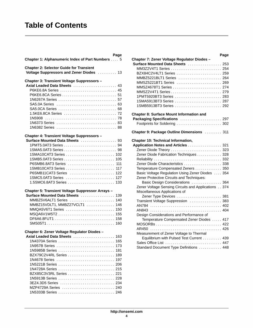
TVS — in Axial Leads
Table 4. Peak Power Dissipation, 500 Watts @ 1 ms SurgeCase 59-04 — Mini Mosorb
CASE 59-04PLASTIC
Cathode = Polarity Band
0 1 2 3 4 5 6
IRSM
IRSM
Time (ms)
Surge Current Characterisitcs
2
(Mini Mosorb )
ELECTRICAL CHARACTERISTICS (TA = 25°C unless otherwise noted) VF = 3.5 V Max, IF = 35 A Pulse(except bidirectional devices).
Working PeakBreakdown Voltage
Maxim m Maxim mWorking PeakReverse
MaximumReverse Maxim m
MaximumReverse VoltageReverse
Voltage VBR @ IT
ReverseLeakage
MaximumReverse S rge
Reverse Voltage@ IRSMVoltage
VRWM
VBR(Volts)
@ ITP lse
Leakage@ VRWM
Reverse SurgeC rrent I RSM
@ IRSM(Clamping Voltage)VRWM
(Volts) Device Min MaxPulse(mA)
@ VRWMIR (µA)
Curren t IRSM(Amps)
(Clamping Voltage)VRSM (Volts)
5 SA5.0A 6.4 7 10 600 54.3 9.26 SA6.0A 6.67 7.37 10 600 48.5 10.3
6.5 SA6.5A 7.22 7.98 10 400 44.7 11.27 SA7.0A 7.78 8.6 10 150 41.7 12
7.5 SA7.5A 8.33 9.21 1 50 38.8 12.98 SA8.0A 8.89 9.83 1 25 36.7 13.6
8.5 SA8.5A 9.44 10.4 1 5 34.7 14.49 SA9.0A 10 11.1 1 1 32.5 15.4
10 SA10A 11.1 12.3 1 1 29.4 1711 SA11A 12.2 13.5 1 1 27.4 18.212 SA12A 13.3 14.7 1 1 25.1 19.913 SA13A 14.4 15.9 1 1 23.2 21.5
14 SA14A 15.6 17.2 1 1 21.5 23.215 SA15A 16.7 18.5 1 1 20.6 24.416 SA16A 17.8 19.7 1 1 19.2 2617 SA17A 18.9 20.9 1 1 18.1 27.6
18 SA18A 20 22.1 1 1 17.2 29.220 SA20A 22.2 24.5 1 1 15.4 32.422 SA22A 24.4 26.9 1 1 14.1 35.524 SA24A 26.7 29.5 1 1 12.8 38.9
26 SA26A 28.9 31.9 1 1 11.9 42.128 SA28A 31.1 34.4 1 1 11 45.430 SA30A 33.3 36.8 1 1 10.3 48.433 SA33A 36.7 40.6 1 1 9.4 53.3
For bidirectional types use CA suffix, SA6.5CA, SA12CA, SA13CA and SA15CA are ON Semiconductor preferred devices.Bi–directional devices have cathode polarity band on each end. (Consult factory for availability).
http://onsemi.com22
TVS — in Axial Leads (continued)
Table 4. Peak Power Dissipation, 500 Watts @ 1 ms SurgeCase 59-04 — Mini Mosorb (continued)
ELECTRICAL CHARACTERISTICS (TA = 25°C unless otherwise noted) VF = 3.5 V Max, IF = 35 A Pulse(except bidirectional devices).
Working PeakBreakdown Voltage
Maxim m Maxim mWorking PeakReverse
MaximumReverse Maxim m
MaximumReverse VoltageReverse
Voltage VBR @ IT
ReverseLeakage
MaximumReverse S rge
Reverse Voltage@ IRSMVoltage
VRWM
VBR(Volts)
@ ITP lse
Leakage@ VRWM
Reverse SurgeC rrent I RSM
@ IRSM(Clamping Voltage)VRWM
(Volts) Device Min MaxPulse(mA)
@ VRWMIR (µA)
Curren t IRSM(Amps)
(Clamping Voltage)VRSM (Volts)
36 SA36A 40 44.2 1 1 8.6 58.140 SA40A 44.4 49.1 1 1 7.8 64.543 SA43A 47.8 52.8 1 1 7.2 69.445 SA45A 50 55.3 1 1 6.9 72.7
48 SA48A 53.3 58.9 1 1 6.5 77.451 SA51A 56.7 62.7 1 1 6.1 82.454 SA54A 60 66.3 1 1 5.7 87.158 SA58A 64.4 71.2 1 1 5.3 93.6
60 SA60A 66.7 73.7 1 1 5.2 96.864 SA64A 71.1 78.6 1 1 4.9 10370 SA70A 77.8 86 1 1 4.4 11375 SA75A 83.3 92.1 1 1 4.1 121
78 SA78A 86.7 95.8 1 1 4 12685 SA85A 94.4 104 1 1 3.6 13790 SA90A 100 111 1 1 3.4 146100 SA100A 111 123 1 1 3.1 162
110 SA110A 122 135 1 1 2.8 177120 SA120A 133 147 1 1 2.5 193130 SA130A 144 159 1 1 2.4 209150 SA150A 167 185 1 1 2.1 243
160 SA160A 178 197 1 1 1.9 259170 SA170A 189 209 1 1 1.8 275
For bidirectional types use CA suffix, SA18CA and SA24CA are ON Semiconductor preferred devices.Bi–directional devices have cathode polarity band on each end. (Consult factory for availability).

http://onsemi.com23
TVS — in Axial Leads (continued)
Table 5. Peak Power Dissipation, 600 Watts @ 1 ms SurgeCase 17 — Surmetic 40
CASE 17PLASTIC
Cathode = Polarity Band
0 1 2 3 4 5 6
IRSM
IRSM
Time (ms)
Surge Current Characterisitcs
2
ELECTRICAL CHARACTERISTICS (TA = 25°C unless otherwise noted) VF = 3.5 V Max, IF = 50 A Pulse(except bidirectional devices).
Breakdownea doVoltage Working Peak
RMaximumR
MaximumR V lt
VBR @ IT
gReverseVoltage
ReverseLeakage
MaximumReverse S rge
Reverse Voltage@ IRSM
BR(Volts)
@ ITPulse
VoltageVRWM
Leakage@ VRWM
Reverse SurgeCurrent I RSM
@ IRSM(Clamping Voltage)
NomPulse(mA) Device
VRWM(Volts)
@ VRWMIR (µA)
Curren t IRSM(Amps)
(Clamping Voltage)VRSM (Volts)Nom (mA) Device (Volts) IR (µA) (Amps ) VRSM (Volts)
6.8 10 P6KE6.8A 5.8 1000 57 10.57.5 10 P6KE7.5A 6.4 500 53 11.38.2 10 P6KE8.2A 7.02 200 50 12.19.1 1 P6KE9.1A 7.78 50 45 13.4
10 1 P6KE10A 8.55 10 41 14.511 1 P6KE11A 9.4 5 38 15.612 1 P6KE12A 10.2 5 36 16.713 1 P6KE13A 11.1 5 33 18.2
15 1 P6KE15A 12.8 5 28 21.216 1 P6KE16A 13.6 5 27 22.518 1 P6KE18A 15.3 5 24 25.220 1 P6KE20A 17.1 5 22 27.7
22 1 P6KE22A 18.8 5 20 30.624 1 P6KE24A 20.5 5 18 33.227 1 P6KE27A 23.1 5 16 37.530 1 P6KE30A 25.6 5 14.4 41.4
33 1 P6KE33A 28.2 5 13.2 45.736 1 P6KE36A 30.8 5 12 49.939 1 P6KE39A 33.3 5 11.2 53.943 1 P6KE43A 36.8 5 10.1 59.3
47 1 P6KE47A 40.2 5 9.3 64.851 1 P6KE51A 43.6 5 8.6 70.156 1 P6KE56A 47.8 5 7.8 7762 1 P6KE62A 53 5 7.1 85
68 1 P6KE68A 58.1 5 6.5 9275 1 P6KE75A 64.1 5 5.8 10382 1 P6KE82A 70.1 5 5.3 11391 1 P6KE91A 77.8 5 4.8 125
100 1 P6KE100A 85.5 5 4.4 137110 1 P6KE110A 94 5 4 152120 1 P6KE120A 102 5 3.6 165130 1 P6KE130A 111 5 3.3 179
For bidirectional types use CA suffix, P6KE7.5CA and P6KE11CA are ON Semiconductor preferred devices.

http://onsemi.com24
TVS — in Axial Leads (continued)
Table 5. Peak Power Dissipation, 600 Watts @ 1 ms SurgeCase 17 — Surmetic 40 (continued)
ELECTRICAL CHARACTERISTICS (TA = 25°C unless otherwise noted) VF = 3.5 V Max, IF = 50 A Pulse(except bidirectional devices).
Breakdownea doVoltage Working Peak
RMaximumR
MaximumR V l
VBR @ IT
gReverseVoltage
ReverseLeakage
MaximumReverse S rge
Reverse Voltage@ IRSM
BR(Volts)
@ ITPulse
VoltageVRWM
Leakage@ VRWM
Reverse SurgeCurrent I RSM
@ IRSM(Clamping Voltage)
NomPulse(mA) Device
VRWM(Volts)
@ VRWMIR (µA)
Curren t IRSM(Amps)
(Clamping Voltage)VRSM (Volts)Nom (mA) Device (Volts) IR (µA) (Amps ) VRSM (Volts)
150 1 P6KE150A 128 5 2.9 207160 1 P6KE160A 136 5 2.7 219170 1 P6KE170A 145 5 2.6 234180 1 P6KE180A 154 5 2.4 246200 1 P6KE200A 171 5 2.2 274
For bidirectional types use CA suffix. Bi–directional devices have cathode polarity band on each end. (Consult factory foravailability).

http://onsemi.com25
TVS — in Axial Leads (continued)
Table 6. Peak Power Dissipation, 1500 Watts @ 1 ms SurgeCase 41A — Mosorb
CASE 41APLASTIC
Cathode = Polarity Band
0 1 2 3 4 5 6
IRSM
IRSM
Time (ms)
Surge Current Characterisitcs
2
ELECTRICAL CHARACTERISTICS (TA = 25°C unless otherwise noted) VF = 3.5 V Max, IF = 100 A Pulse)ELECTRICAL CHARACTERISTICS (C suffix denotes standard back to back bidirectional versions. Test both polarities)
Clamping Voltage (9)
MaxReverseStand-
BreakdownVoltage
MaximumMaximumReverse
MaximumReverse
Voltage @IRSM
PeakPulse
Current @
PeakPulse
Current @Ipp2 =Stand-
OffVoltageVRWM(Volts)
JEDECDevice Device
VBRVoltsMin
@ ITPulse(mA)
Maxim umReverseLeakage@ VRWMIR (µA)
ReverseSurge
CurrentIRSM
(Volts)
IRSM(ClampingVoltage)
VRSM(Volts)
Current @Ipp1 = 1 A
VC1(Voltsmax)
Ipp2 =10 AVC2
(Voltsmax)
5 1N5908 6 1 300 120 8.5 7.6 @30 A
8 @60 A
5 1N6373 ICTE-5/MPTE-5 6 1 300 160 9.4 7.1 7.58 1N6374 ICTE-8/MPTE-8 9.4 1 25 100 15 11.3 11.58 1N6382 ICTE-8C/MPTE-8C 9.4 1 25 100 15 11.4 11.6
10 1N6375 ICTE-10/MPTE-10 11.7 1 2 90 16.7 13.7 14.110 1N6383 ICTE-10C/MPTE-10C 11.7 1 2 90 16.7 14.1 14.512 1N6376 ICTE-12/MPTE-12 14.1 1 2 70 21.2 16.1 16.512 1N6384 ICTE-12C/MPTE-12C 14.1 1 2 70 21.2 16.7 17.1
15 1N6377 ICTE-15/MPTE-15 17.6 1 2 60 25 20.1 20.615 1N6385 ICTE-15C/MPTE-15C 17.6 1 2 60 25 20.8 21.418 1N6378 ICTE-18/MPTE-18 21.2 1 2 50 30 24.2 25.218 1N6386 ICTE-18C/MPTE-18C 21.2 1 2 50 30 24.8 25.5
22 1N6379 ICTE-22/MPTE-22 25.9 1 2 40 37.5 29.8 3222 1N6387 ICTE-22C/MPTE-22C 25.9 1 2 40 37.5 30.8 3236 1N6380 ICTE-36/MPTE-36 42.4 1 2 23 65.2 50.6 54.336 1N6388 ICTE-36C/MPTE-36C 42.4 1 2 23 65.2 50.6 54.3
45 1N6381 ICTE-45/MPTE-45 52.9 1 2 19 78.9 63.3 7045 1N6389 ICTE-45C/MPTE-45C 52.9 1 2 19 78.9 63.3 70
1N6382 thru 1N6389 and C suffix ICTE/MPTE device types are bidirectional. Bi–directional devices have cathode polarity band on eachend. All other device types are unidirectional only. (Consult factory for availability)
http://onsemi.com26
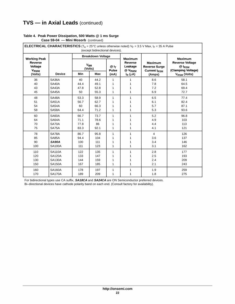
TVS — in Axial Leads (continued)
Table 7. Peak Power Dissipation, 1500 Watts @ 1 ms SurgeCase 41A – Mosorb
0 1 2 3 4 5 6
IRSM
IRSM
Time (ms)
Surge Current Characterisitcs
2
CASE 41APLASTIC
Cathode = Polarity Band
ELECTRICAL CHARACTERISTICS (TA = 25°C unless otherwise noted) VF = 3.5 V Max, IF = 100 A Pulse
Breakdown VoltageWorking Maxim m
MaximumReverseV lt
VBRVolts @ IT
WorkingPeak
ReverseVoltage
MaximumReverseLeakage
MaximumReverseSurge
Current
Voltage@ IRSM
(ClampingVoltage)
Nom
@ ITPulse(mA)
JEDECDevice Device
VoltageVRWM(Volts)
Leakage@ VRWMIR (µA)
CurrentIRSM
(Amps)
Voltage)VRSM(Volts)
6.8 10 1N6267A 1.5KE6.8A 5.8 1000 143 10.57.5 10 1N6268A 1.5KE7.5A 6.4 500 132 11.38.2 10 1N6269A 1.5KE8.2A 7.02 200 124 12.19.1 1 1N6270A 1.5KE9.1A 7.78 50 112 13.4
10 1 1N6271A 1.5KE10A 8.55 10 103 14.511 1 1N6272A 1.5KE11A 9.4 5 96 15.612 1 1N6273A 1.5KE12A 10.2 5 90 16.713 1 1N6274A 1.5KE13A 11.1 5 82 18.2
15 1 1N6275A 1.5KE15A 12.8 5 71 21.216 1 1N6276A 1.5KE16A 13.6 5 67 22.518 1 1N6277A 1.5KE18A 15.3 5 59.5 25.220 1 1N6278A 1.5KE20A 17.1 5 54 27.7
22 1 1N6279A 1.5KE22A 18.8 5 49 30.624 1 1N6280A 1.5KE24A 20.5 5 45 33.227 1 1N6281A 1.5KE27A 23.1 5 40 37.530 1 1N6282A 1.5KE30A 25.6 5 36 41.4
33 1 1N6283A 1.5KE33A 28.2 5 33 45.736 1 1N6284A 1.5KE36A 30.8 5 30 49.939 1 1N6285A 1.5KE39A 33.3 5 28 53.943 1 1N6286A 1.5KE43A 36.8 5 25.3 59.3
47 1 1N6287A 1.5KE47A 40.2 5 23.2 64.851 1 1N6288A 1.5KE51A 43.6 5 21.4 70.156 1 1N6289A 1.5KE56A 47.8 5 19.5 7762 1 1N6290A 1.5KE62A 53 5 17.7 85
68 1 1N6291A 1.5KE68A 58.1 5 16.3 9275 1 1N6292A 1.5KE75A 64.1 5 14.6 10382 1 1N6293A 1.5KE82A 70.1 5 13.3 11391 1 1N6294A 1.5KE91A 77.8 5 12 125
100 1 1N6295A 1.5KE100A 85.5 5 11 137110 1 1N6296A 1.5KE110A 94 5 9.9 152120 1 1N6297A 1.5KE120A 102 5 9.1 165130 1 1N6298A 1.5KE130A 111 5 8.4 179
For bidirectional types use CA suffix on 1.5KE series only. Bi–directional devices have cathode polarity band on each end.(Consult factory for availability) 1N6267-6303A series do not have CA option since the CA is not included in EIA Registration.

http://onsemi.com27
TVS — in Axial Leads (continued)
Table 7. Peak Power Dissipation, 1500 Watts @ 1 ms SurgeCase 41A – Mosorb (continued)
ELECTRICAL CHARACTERISTICS (TA = 25°C unless otherwise noted) VF = 3.5 V Max, IF = 100 A Pulse
Breakdown VoltageWorking Maxim m
MaximumReverseV lt
VBRVolts @ IT
WorkingPeak
ReverseVoltage
MaximumReverseLeakage
MaximumReverseSurge
Current
Voltage@ IRSM
(ClampingVoltage)
Nom
@ ITPulse(mA)
JEDECDevice Device
VoltageVRWM(Volts)
Leakage@ VRWMIR (µA)
CurrentIRSM
(Amps)
Voltage)VRSM(Volts)
150 1 1N6299A 1.5KE150A 128 5 7.2 207160 1 1N6300A 1.5KE160A 136 5 6.8 219170 1 1N6301A 1.5KE170A 145 5 6.4 234180 1 1N6302A 1.5KE180A 154 5 6.1 246200 1 1N6303A 1.5KE200A 171 5 5.5 274220 1 1.5KE220A 185 5 4.6 328250 1 1.5KE250A 214 5 5 344
For bidirectional types use CA suffix. Bi–directional devices have cathode polarity band on each end. (Consult factory foravailability). 1N6267-6303A series do not have CA option since the CA is not included in EIA Registration.

http://onsemi.com28
TVS — in Surface Mount
Table 8. 1PMT Series Unidirectional Overvoltage Transient Suppressors, 175 Watts Peak Power@ 1 ms Surge
ELECTRICAL CHARACTERISTICS (TL = 30C unless otherwise noted) (VF = 1.25 Volts @ 200 mA)
Device MarkingVRWM (V) VBR @ IT (V) (Note 2.) IT IR @ VRWM VC @ IPP IPP (A)
Device Marking(Note 1.) Min Nom Max (mA) (µA) (V) (Note 3.)
POWERMITECASE 457–04
PLASTIC 0 1 2 3 4 5 6
IRSM
IRSM
Time (ms)
Surge Current Characterisitcs
2
1PMT5.0AT3 MKE 5.0 6.4 6.7 7.0 10 800 9.2 191PMT7.0AT3 MKM 7.0 7.78 8.2 8.6 10 500 12 14.61PMT12AT3 MLE 12 13.3 14 14.7 1.0 5.0 19.9 8.81PMT16AT3 MLP 16 17.8 18.75 19.7 1.0 5.0 26 7.0
1PMT18AT3 MLT 18 20 21 22.1 1.0 5.0 29.2 6.01PMT22AT3 MLX 22 24.4 25.6 26.9 1.0 5.0 35.5 4.91PMT24AT3 MLZ 24 26.7 28.1 29.5 1.0 5.0 38.9 4.51PMT26AT3 MME 26 28.9 30.4 31.9 1.0 5.0 42.1 4.2
1PMT28AT3 MMG 28 31.1 32.8 34.4 1.0 5.0 45.4 3.91PMT30AT3 MMK 30 33.3 35.1 36.8 1.0 5.0 48.4 3.61PMT33AT3 MMM 33 36.7 38.7 40.6 1.0 5.0 53.3 3.31PMT36AT3 MMP 36 40 42.1 44.2 1.0 5.0 58.1 3.0
1PMT40AT3 MMR 40 44.4 46.8 49.1 1.0 5.0 64.5 2.71PMT48AT3 MMX 48 53.3 56.1 58.9 1.0 5.0 77.4 2.31PMT51AT3 MMZ 51 56.7 59.7 62.7 1.0 5.0 82.4 2.11PMT58AT3 MNG 58 64.4 67.8 71.2 1.0 5.0 93.6 1.9
1. A transient suppressor is normally selected according to the Working Peak Reverse Voltage (VRWM) which should be equal to orgreater than the DC or continuous peak operating voltage level.
2. VBR measured at pulse test current IT at ambient temperature of 25C.3. 10 x 1000 µs exponential decay surge waveform.

http://onsemi.com29
TVS — in Surface Mount (continued)
Table 9. 1SMA Series Unidirectional Overvoltage Transient Suppressors; 400 Watts Peak Power@ 1 ms Surge
ELECTRICAL CHARACTERISTICS (VF = 3.5 Volts @ IF = 40 A for all types)
WorkingPeak
Breakdown Voltage MaximumReverse Voltage
MaximumReverse
Maximum
DevicePeak
ReverseVoltage V RWM
(Volts)
VBRVolts(Min)
ITmA
Reverse Voltage@ IRSM
(Clamping Volt-age) VC (Volts)
ReverseSurge Current
IPP(Amps)
Maxim umReverse Leakage
@ VRWMIR (µA)
DeviceMarking
SMACASE 403B–01
PLASTIC 0 1 2 3 4 5 6
IRSM
IRSM
Time (ms)
Surge Current Characterisitcs
2
1SMA5.0AT3 5.0 6.4 10 9.2 43.5 400 QE1SMA6.0AT3 6.0 6.67 10 10.3 38.8 400 QG1SMA6.5AT3 6.5 7.22 10 11.2 35.7 250 QK1SMA7.0AT3 7.0 7.78 10 12.0 33.3 250 QM
1SMA7.5AT3 7.5 8.33 1 12.9 31.0 50 QP1SMA8.0AT3 8.0 8.89 1 13.6 29.4 25 QR1SMA8.5AT3 8.5 9.44 1 14.4 27.8 5.0 QT1SMA9.0AT3 9.0 10 1 15.4 26.0 2.5 QV
1SMA10AT3 10 11.1 1 17.0 23.5 2.5 QX1SMA11AT3 11 12.2 1 18.2 22.0 2.5 QZ1SMA12AT3 12 13.3 1 19.9 20.1 2.5 RE1SMA13AT3 13 14.4 1 21.5 18.6 2.5 RG
1SMA14AT3 14 15.6 1 23.2 17.2 2.5 RK1SMA15AT3 15 16.7 1 24.4 16.4 2.5 RM1SMA16AT3 16 17.8 1 26.0 15.4 2.5 RP1SMA17AT3 17 18.9 1 27.6 14.5 2.5 RR
1SMA18AT3 18 20 1 29.2 13.7 2.5 RT1SMA20AT3 20 22.2 1 32.4 12.3 2.5 RV1SMA22AT3 22 24.4 1 35.5 11.3 2.5 RX1SMA24AT3 24 26.7 1 38.9 10.3 2.5 RZ
1SMA26AT3 26 28.9 1 42.1 9.5 2.5 SE1SMA28AT3 28 31.1 1 45.4 8.8 2.5 SG1SMA30AT3 30 33.3 1 48.4 8.3 2.5 SK1SMA33AT3 33 36.7 1 53.3 7.5 2.5 SM
1SMA36AT3 36 40 1 58.1 6.9 2.5 SP1SMA40AT3 40 44.4 1 64.5 6.2 2.5 SR1SMA43AT3 43 47.8 1 69.4 5.8 2.5 ST1SMA45AT3 45 50 1 72.2 5.5 2.5 SV
1SMA48AT3 48 53.3 1 77.4 5.2 2.5 SX1SMA51AT3 51 56.7 1 82.4 4.9 2.5 SZ1SMA54AT3 54 60 1 87.1 4.6 2.5 TE1SMA58AT3 58 64.4 1 93.6 4.8 2.5 TG
1SMA60AT3 60 66.7 1 96.8 4.1 2.5 TK1SMA64AT3 64 71.1 1 103.0 3.9 2.5 TM1SMA70AT3 70 77.8 1 113.0 3.5 2.5 TP1SMA75AT3 75 83.3 1 121.0 3.3 2.5 TR1SMA78AT3 78 86.7 1 126.0 3.2 2.5 TS

http://onsemi.com30
TVS — in Surface Mount (continued)
Table 10. 1SMA Series Bidirectional Zener Overvoltage Transient Suppressors; 400 Watts Peak Power@ 1 ms Surge
ELECTRICAL CHARACTERISTICS
WorkingPeak
Breakdown Voltage MaximumReverse Voltage
MaximumReverse Maximum
DevicePeak
ReverseVoltage V RWM
(Volts)
VBRVolts(Min)
ITmA
Reverse Voltage@ IRSM
(ClampingVoltage)
VC (Volts)
ReverseSurge Cur-
rent I PP(Amps)
Maxim umReverse Leakage
@ VRWMIR (µA)
DevceMarking
SMACASE 403B–01
PLASTIC 0 1 2 3 4 5 6
IRSM
IRSM
Time (ms)
Surge Current Characterisitcs
2
1SMA10CAT3 10 11.1 1 17.0 23.5 2.5 QXC1SMA11CAT3 11 12.2 1 18.2 22.0 2.5 QZC1SMA12CAT3 12 13.3 1 19.9 20.1 2.5 REC1SMA13CAT3 13 14.4 1 21.5 18.6 2.5 RGC
1SMA14CAT3 14 15.6 1 23.2 17.2 2.5 RKC1SMA15CAT3 15 16.7 1 24.4 16.4 2.5 RMC1SMA16CAT3 16 17.8 1 26.0 15.4 2.5 RPC1SMA17CAT3 17 18.9 1 27.6 14.5 2.5 RRC
1SMA18CAT3 18 20 1 29.2 13.7 2.5 RTC1SMA20CAT3 20 22.2 1 32.4 12.3 2.5 RVC1SMA22CAT3 22 24.4 1 35.5 11.3 2.5 RXC1SMA24CAT3 24 26.7 1 38.9 10.3 2.5 RZC
1SMA26CAT3 26 28.9 1 42.1 9.5 2.5 SEC1SMA28CAT3 28 31.1 1 45.4 8.8 2.5 SGC1SMA30CAT3 30 33.3 1 48.4 8.3 2.5 SKC1SMA33CAT3 33 36.7 1 53.3 7.5 2.5 SMC
1SMA36CAT3 36 40 1 58.1 6.9 2.5 SPC1SMA40CAT3 40 44.4 1 64.5 6.2 2.5 SRC1SMA43CAT3 43 47.8 1 69.4 5.8 2.5 STC1SMA45CAT3 45 50 1 72.2 5.5 2.5 SVC
1SMA48CAT3 48 53.3 1 77.4 5.2 2.5 SXC1SMA51CAT3 51 56.7 1 82.4 4.9 2.5 SZC1SMA54CAT3 54 60 1 87.1 4.6 2.5 TEC1SMA58CAT3 58 64.4 1 93.6 4.3 2.5 TGC
1SMA60CAT3 60 66.7 1 96.8 4.1 2.5 TKC1SMA64CAT3 64 71.1 1 103.0 3.9 2.5 TMC1SMA70CAT3 70 77.8 1 113.0 3.5 2.5 TPC1SMA75CAT3 75 83.3 1 121.0 3.3 2.5 TRC1SMA78CAT3 78 86.7 1 126.0 3.2 2.5 TSC
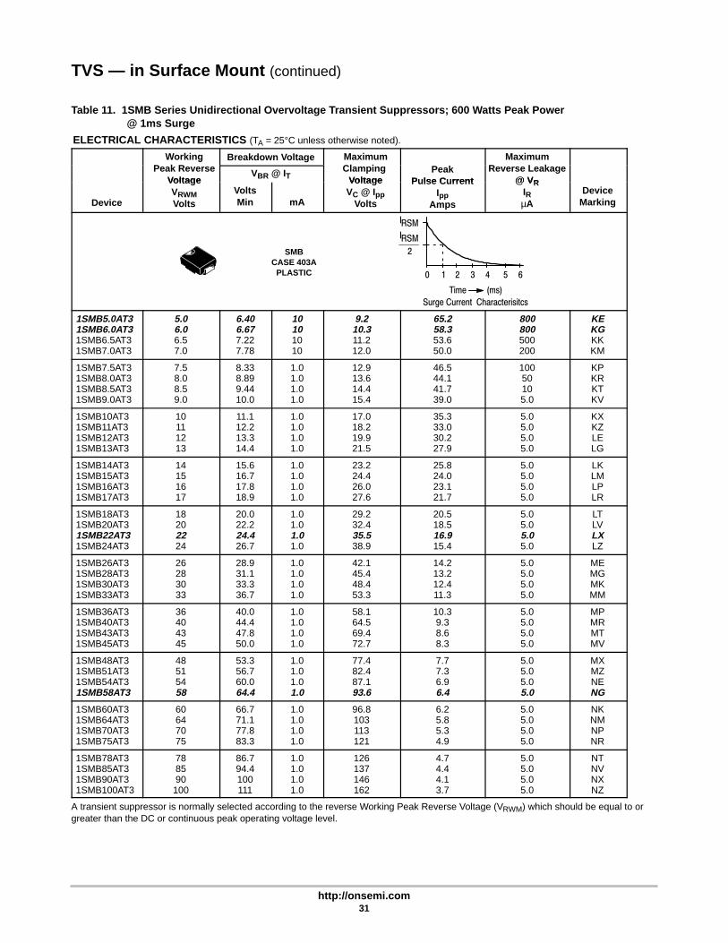
http://onsemi.com31
TVS — in Surface Mount (continued)
Table 11. 1SMB Series Unidirectional Overvoltage Transient Suppressors; 600 Watts Peak Power@ 1ms Surge
ELECTRICAL CHARACTERISTICS (TA = 25°C unless otherwise noted).
WorkingP k R
Breakdown Voltage MaximumCl i
MaximumR L k
gPeak Reverse
VoltageVBR @ IT
Clamping Voltage
PeakP lse C rrent
Reverse Leakage@ VR
Device
VoltageVRWMVolts
VoltsMin mA
VoltageVC @ Ipp
Volts
Pulse Curren tIpp
Amps
@ VRIRµA
DeviceMarking
SMBCASE 403A
PLASTIC 0 1 2 3 4 5 6
IRSM
IRSM
Time (ms)
Surge Current Characterisitcs
2
1SMB5.0AT31SMB6.0AT31SMB6.5AT31SMB7.0AT3
5.06.06.57.0
6.406.677.227.78
10101010
9.210.311.212.0
65.258.353.650.0
800800500200
KEKGKKKM
1SMB7.5AT31SMB8.0AT31SMB8.5AT31SMB9.0AT3
7.58.08.59.0
8.338.899.4410.0
1.01.01.01.0
12.913.614.415.4
46.544.141.739.0
10050105.0
KPKRKTKV
1SMB10AT31SMB11AT31SMB12AT31SMB13AT3
10111213
11.112.213.314.4
1.01.01.01.0
17.018.219.921.5
35.333.030.227.9
5.05.05.05.0
KXKZLELG
1SMB14AT31SMB15AT31SMB16AT31SMB17AT3
14151617
15.616.717.818.9
1.01.01.01.0
23.224.426.027.6
25.824.023.121.7
5.05.05.05.0
LKLMLPLR
1SMB18AT31SMB20AT31SMB22AT31SMB24AT3
18202224
20.022.224.426.7
1.01.01.01.0
29.232.435.538.9
20.518.516.915.4
5.05.05.05.0
LTLVLXLZ
1SMB26AT31SMB28AT31SMB30AT31SMB33AT3
26283033
28.931.133.336.7
1.01.01.01.0
42.145.448.453.3
14.213.212.411.3
5.05.05.05.0
MEMGMKMM
1SMB36AT31SMB40AT31SMB43AT31SMB45AT3
36404345
40.044.447.850.0
1.01.01.01.0
58.164.569.472.7
10.39.38.68.3
5.05.05.05.0
MPMRMTMV
1SMB48AT31SMB51AT31SMB54AT31SMB58AT3
48515458
53.356.760.064.4
1.01.01.01.0
77.482.487.193.6
7.77.36.96.4
5.05.05.05.0
MXMZNENG
1SMB60AT31SMB64AT31SMB70AT31SMB75AT3
60647075
66.771.177.883.3
1.01.01.01.0
96.8103113121
6.25.85.34.9
5.05.05.05.0
NKNMNPNR
1SMB78AT31SMB85AT31SMB90AT31SMB100AT3
788590100
86.794.4100111
1.01.01.01.0
126137146162
4.74.44.13.7
5.05.05.05.0
NTNVNXNZ
A transient suppressor is normally selected according to the reverse Working Peak Reverse Voltage (VRWM) which should be equal to orgreater than the DC or continuous peak operating voltage level.

http://onsemi.com32
TVS — in Surface Mount (continued)
Table 11. 1SMB Series Unidirectional Overvoltage Transient Suppressors; 600 Watts Peak Power@ 1 ms Surge (continued)
ELECTRICAL CHARACTERISTICS (TA = 25°C unless otherwise noted).
WorkingP k R
Breakdown Voltage MaximumCl i
MaximumR L k
gPeak Reverse
VoltageVBR @ IT
Clamping Voltage
PeakP lse C rrent
Reverse Leakage@ VR
Device
VoltageVRWMVolts
VoltsMin mA
VoltageVC @ Ipp
Volts
Pulse Curren tIpp
Amps
@ VRIRµA
DeviceMarking
SMBCASE 403A
PLASTIC 0 1 2 3 4 5 6
IRSM
IRSM
Time (ms)
Surge Current Characterisitcs
2
1SMB110AT31SMB120AT31SMB130AT31SMB150AT3
110120130150
122133144167
1.01.01.01.0
177193209243
3.43.12.92.5
5.05.05.05.0
PEPGPKPM
1SMB160AT31SMB170AT3
160170
178189
1.01.0
259275
2.32.2
5.05.0
PPPR
A transient suppressor is normally selected according to the reverse Working Peak Reverse Voltage (VRWM) which should be equal to orgreater than the DC or continuous peak operating voltage level.

http://onsemi.com33
TVS — in Surface Mount (continued)
Table 12. 1SMB Series Bidirectional Overvoltage Transient Suppressors; 600 Watts Peak Power@ 1ms Surge
ELECTRICAL CHARACTERISTICS (TA = 25°C unless otherwise noted).
WorkingP k R
Breakdown Voltage MaximumCl i
MaximumR L k
gPeak Reverse
VoltageVBR @ IT
Clamping Voltage
PeakP lse C rrent
Reverse Leakage@ VR
Device
VoltageVRWMVolts
VoltsMin mA
VoltageVC @ Ipp
Volts
Pulse Curren tIpp
Amps
@ VRIRµA
DeviceMarking
SMBCASE 403A
PLASTIC 0 1 2 3 4 5 6
IRSM
IRSM
Time (ms)
Surge Current Characterisitcs
2
1SMB10CAT31SMB11CAT31SMB12CAT31SMB13CAT3
10111213
11.112.213.314.4
1.01.01.01.0
17.018.219.921.5
35.333.030.227.9
5.05.05.05.0
KXCKZCLECLGC
1SMB14CAT31SMB15CAT31SMB16CAT31SMB17CAT3
14151617
15.616.717.818.9
1.01.01.01.0
23.224.426.027.6
25.824.023.121.7
5.05.05.05.0
LKCLMCLPCLRC
1SMB18CAT31SMB20CAT31SMB22CAT31SMB24CAT3
18202224
20.022.224.426.7
1.01.01.01.0
29.232.435.538.9
20.518.516.915.4
5.05.05.05.0
LTCLVCLXCLZC
1SMB26CAT31SMB28CAT31SMB30CAT31SMB33CAT3
26283033
28.931.133.336.7
1.01.01.01.0
42.145.448.453.3
14.213.212.411.3
5.05.05.05.0
MECMGCMKCMMC
1SMB36CAT31SMB40CAT31SMB43CAT31SMB45CAT3
36404345
40.044.447.850.0
1.01.01.01.0
58.164.569.472.7
10.39.38.68.3
5.05.05.05.0
MPCMRCMTCMVC
1SMB48CAT31SMB51CAT31SMB54CAT31SMB58CAT3
48515458
53.356.760.064.4
1.01.01.01.0
77.482.487.193.6
7.77.36.96.4
5.05.05.05.0
MXCMZCNECNGC
1SMB60CAT31SMB64CAT31SMB70CAT31SMB75CAT3
60647075
66.771.177.883.3
1.01.01.01.0
96.8103113121
6.25.85.34.9
5.05.05.05.0
NKCNMCNPCNRC
1SMB78CAT3 78 86.7 1.0 126 4.7 5.0 NTC
A transient suppressor is normally selected according to the reverse Working Peak Reverse Voltage (VRWM) which should be equal to orgreater than the DC or continuous peak operating voltage level.
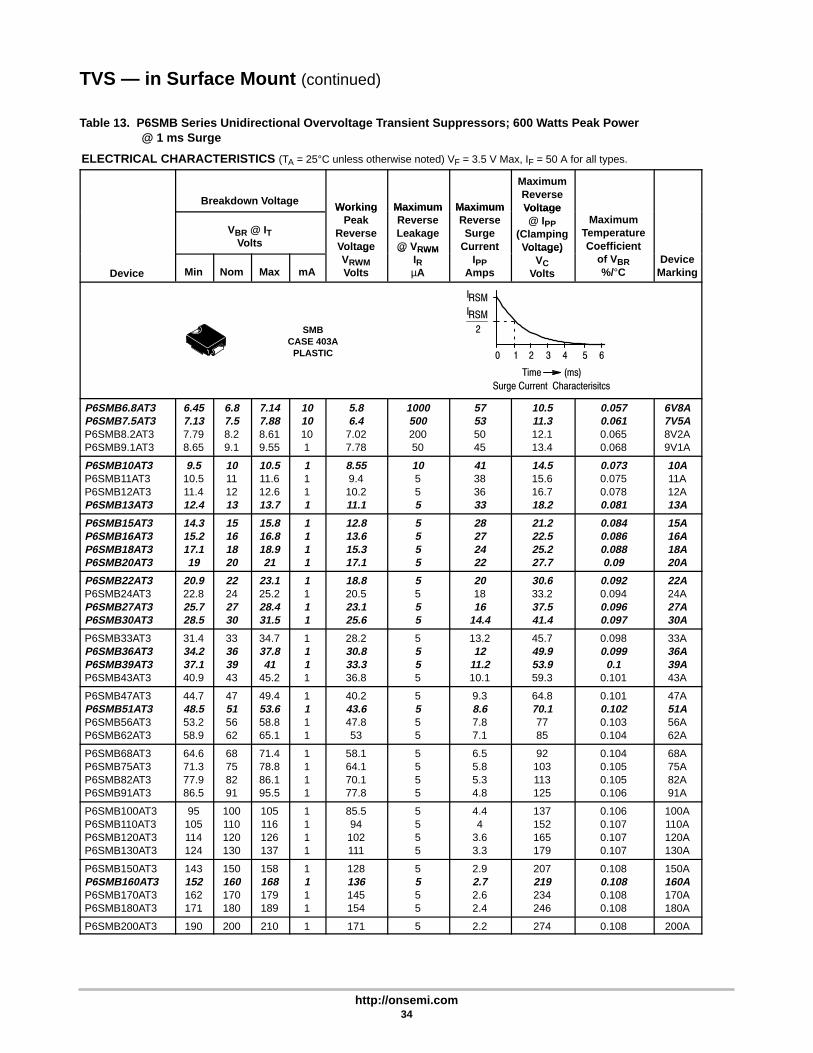
http://onsemi.com34
TVS — in Surface Mount (continued)
Table 13. P6SMB Series Unidirectional Overvoltage Transient Suppressors; 600 Watts Peak Power@ 1 ms Surge
ELECTRICAL CHARACTERISTICS (TA = 25°C unless otherwise noted) VF = 3.5 V Max, IF = 50 A for all types.
Breakdown Voltage Workin g Maximum Maximum
MaximumReverseVolta ge
VBR @ ITVolts
WorkingPeak
ReverseVoltage
Maxim umReverseLeakage@ VRWM
Maxim umReverseSurge
Current
Voltage@ IPP
(ClampingVoltage)
MaximumTemperatureCoefficient
Device Min Nom Max mA
VoltageVRWMVolts
@ VRWMIRµA
CurrentIPP
Amps
Voltage)VC
Volts
Coefficientof VBR%/°C
DeviceMarking
SMBCASE 403A
PLASTIC 0 1 2 3 4 5 6
IRSM
IRSM
Time (ms)
Surge Current Characterisitcs
2
P6SMB6.8AT3P6SMB7.5AT3P6SMB8.2AT3P6SMB9.1AT3
6.457.137.798.65
6.87.58.29.1
7.147.888.619.55
1010101
5.86.47.027.78
100050020050
57535045
10.511.312.113.4
0.0570.0610.0650.068
6V8A7V5A8V2A9V1A
P6SMB10AT3P6SMB11AT3P6SMB12AT3P6SMB13AT3
9.510.511.412.4
10111213
10.511.612.613.7
1111
8.559.410.211.1
10555
41383633
14.515.616.718.2
0.0730.0750.0780.081
10A11A12A13A
P6SMB15AT3P6SMB16AT3P6SMB18AT3P6SMB20AT3
14.315.217.119
15161820
15.816.818.921
1111
12.813.615.317.1
5555
28272422
21.222.525.227.7
0.0840.0860.0880.09
15A16A18A20A
P6SMB22AT3P6SMB24AT3P6SMB27AT3P6SMB30AT3
20.922.825.728.5
22242730
23.125.228.431.5
1111
18.820.523.125.6
5555
201816
14.4
30.633.237.541.4
0.0920.0940.0960.097
22A24A27A30A
P6SMB33AT3P6SMB36AT3P6SMB39AT3P6SMB43AT3
31.434.237.140.9
33363943
34.737.841
45.2
1111
28.230.833.336.8
5555
13.212
11.210.1
45.749.953.959.3
0.0980.0990.1
0.101
33A36A39A43A
P6SMB47AT3P6SMB51AT3P6SMB56AT3P6SMB62AT3
44.748.553.258.9
47515662
49.453.658.865.1
1111
40.243.647.853
5555
9.38.67.87.1
64.870.17785
0.1010.1020.1030.104
47A51A56A62A
P6SMB68AT3P6SMB75AT3P6SMB82AT3P6SMB91AT3
64.671.377.986.5
68758291
71.478.886.195.5
1111
58.164.170.177.8
5555
6.55.85.34.8
92103113125
0.1040.1050.1050.106
68A75A82A91A
P6SMB100AT3P6SMB110AT3P6SMB120AT3P6SMB130AT3
95105114124
100110120130
105116126137
1111
85.594102111
5555
4.44
3.63.3
137152165179
0.1060.1070.1070.107
100A110A120A130A
P6SMB150AT3P6SMB160AT3P6SMB170AT3P6SMB180AT3
143152162171
150160170180
158168179189
1111
128136145154
5555
2.92.72.62.4
207219234246
0.1080.1080.1080.108
150A160A170A180A
P6SMB200AT3 190 200 210 1 171 5 2.2 274 0.108 200A
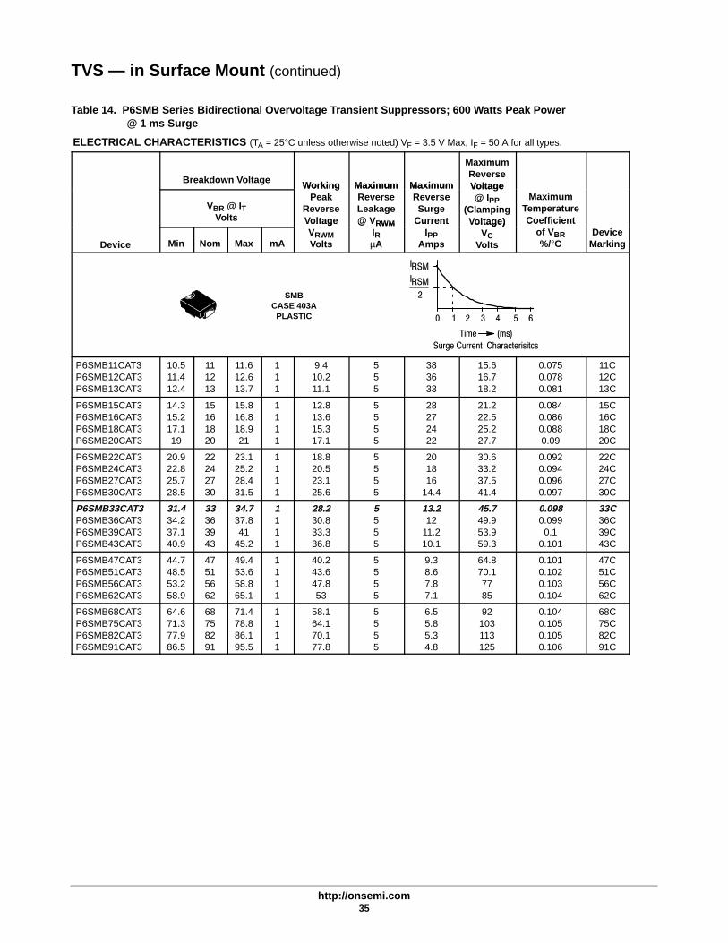
http://onsemi.com35
TVS — in Surface Mount (continued)
Table 14. P6SMB Series Bidirectional Overvoltage Transient Suppressors; 600 Watts Peak Power@ 1 ms Surge
ELECTRICAL CHARACTERISTICS (TA = 25°C unless otherwise noted) VF = 3.5 V Max, IF = 50 A for all types.
Breakdown Voltage Workin g Maximum Maximum
MaximumReverseVolta ge
VBR @ ITVolts
WorkingPeak
ReverseVoltage
Maxim umReverseLeakage@ VRWM
Maxim umReverseSurge
Current
Voltage@ IPP
(ClampingVoltage)
MaximumTemperatureCoefficient
Device Min Nom Max mA
VoltageVRWMVolts
@ VRWMIRµA
CurrentIPP
Amps
Voltage)VC
Volts
Coefficientof VBR%/°C
DeviceMarking
SMBCASE 403A
PLASTIC 0 1 2 3 4 5 6
IRSM
IRSM
Time (ms)
Surge Current Characterisitcs
2
P6SMB11CAT3P6SMB12CAT3P6SMB13CAT3
10.511.412.4
111213
11.612.613.7
111
9.410.211.1
555
383633
15.616.718.2
0.0750.0780.081
11C12C13C
P6SMB15CAT3P6SMB16CAT3P6SMB18CAT3P6SMB20CAT3
14.315.217.119
15161820
15.816.818.921
1111
12.813.615.317.1
5555
28272422
21.222.525.227.7
0.0840.0860.0880.09
15C16C18C20C
P6SMB22CAT3P6SMB24CAT3P6SMB27CAT3P6SMB30CAT3
20.922.825.728.5
22242730
23.125.228.431.5
1111
18.820.523.125.6
5555
201816
14.4
30.633.237.541.4
0.0920.0940.0960.097
22C24C27C30C
P6SMB33CAT3P6SMB36CAT3P6SMB39CAT3P6SMB43CAT3
31.434.237.140.9
33363943
34.737.841
45.2
1111
28.230.833.336.8
5555
13.212
11.210.1
45.749.953.959.3
0.0980.0990.1
0.101
33C36C39C43C
P6SMB47CAT3P6SMB51CAT3P6SMB56CAT3P6SMB62CAT3
44.748.553.258.9
47515662
49.453.658.865.1
1111
40.243.647.853
5555
9.38.67.87.1
64.870.17785
0.1010.1020.1030.104
47C51C56C62C
P6SMB68CAT3P6SMB75CAT3P6SMB82CAT3P6SMB91CAT3
64.671.377.986.5
68758291
71.478.886.195.5
1111
58.164.170.177.8
5555
6.55.85.34.8
92103113125
0.1040.1050.1050.106
68C75C82C91C

http://onsemi.com36
TVS — in Surface Mount (continued)
Table 15. ISMC Series Unidirectional Overvoltage Transient Suppressors; 1500 Watts Peak Power@ 1 ms Surge
ELECTRICAL CHARACTERISTICS (TA = 25°C unless otherwise noted).
WorkingPeak
Breakdown Voltage*Maximum MaximumPeak
ReverseVoltage
VBR @ ITMaximumClamping
VoltagePeak
P lse C rrent
MaximumReverse Leakage
@ V
Device
VoltageVR
Volts
VoltsMin mA
VoltageVC @ Ipp
Volts
Pulse CurrentIpp
Amps
@ VRIRµA
DeviceMarking
SMCCASE 403B
PLASTIC 0 1 2 3 4 5 6
IRSM
IRSM
Time (ms)
Surge Current Characterisitcs
2
1SMC5.0AT31SMC6.0AT31SMC6.5AT31SMC7.0AT3
5.06.06.57.0
6.406.677.227.78
10101010
9.210.311.212.0
163.0145.6133.9125.0
10001000500200
GDEGDGGDKGDM
1SMC7.5AT31SMC8.0AT31SMC8.5AT31SMC9.0AT3
7.58.08.59.0
8.338.899.4410.0
1.01.01.01.0
12.913.614.415.4
116.3110.3104.297.4
100502010
GDPGDRGDTGDV
1SMC10AT31SMC11AT31SMC12AT31SMC13AT3
10111213
11.112.213.314.4
1.01.01.01.0
17.018.219.921.5
88.282.475.369.7
5.05.05.05.0
GDXGDZGEEGEG
1SMC14AT31SMC15AT31SMC16AT31SMC17AT3
14151617
15.616.717.818.9
1.01.01.01.0
23.224.426.027.6
64.761.557.753.3
5.05.05.05.0
GEKGEMGEPGER
1SMC18AT31SMC20AT31SMC22AT31SMC24AT3
18202224
20.022.224.426.7
1.01.01.01.0
29.232.435.538.9
51.446.342.238.6
5.05.05.05.0
GETGEVGEXGEZ
1SMC26AT31SMC28AT31SMC30AT31SMC33AT3
26283033
28.931.133.336.7
1.01.01.01.0
42.145.448.453.3
35.633.031.028.1
5.05.05.05.0
GFEGFGGFKGFM
1SMC36AT31SMC40AT31SMC43AT31SMC45AT3
36404345
40.044.447.850.0
1.01.01.01.0
58.164.569.472.7
25.823.221.620.6
5.05.05.05.0
GFPGFRGFTGFV
1SMC48AT31SMC51AT31SMC54AT31SMC58AT3
48515458
53.356.760.064.4
1.01.01.01.0
77.482.487.193.6
19.418.217.216.0
5.05.05.05.0
GFXGFZGGEGGG
1SMC60AT31SMC64AT31SMC70AT31SMC75AT3
60647075
66.771.177.883.3
1.01.01.01.0
96.8103113121
15.514.613.312.4
5.05.05.05.0
GGKGGMGGPGGR
1SMC78AT3 78 86.7 1.0 126 11.4 5.0 GGT
A transient suppressor is normally selected according to the reverse Working Peak Reverse Voltage (VRWM) which should be equal to orgreater than the DC or continuous peak operating voltage level.

http://onsemi.com37
TVS — in Surface Mount (continued)
Table 16. 1.5 SMC Series Unidirectional Overvoltage Transient Suppressors; 1500 Watts Peak Power@ 1 ms Surge
ELECTRICAL CHARACTERISTICS (TA = 25°C unless otherwise noted) VF = 3.5 V Max, IF = 100 A for all types.
Breakdown Voltage Workin g Maximum Maximum
MaximumReverseVolta ge
VBR @ ITVolts
WorkingPeak
ReverseVoltage
Maxim umReverseLeakage@ VRWM
Maxim umReverseSurge
Current
Voltage@ IPP
(ClampingVoltage)
MaximumTemperatureCoefficient
Device Min Nom Max mA
VoltageVRWMVolts
@ VRWMIRµA
CurrentIPP
Amps
Voltage)VC
Volts
Coefficientof VBR%/°C
DeviceMarking
SMCCASE 403PLASTIC 0 1 2 3 4 5 6
IRSM
IRSM
Time (ms)
Surge Current Characterisitcs
2
1.5SMC6.8AT31.5SMC7.5AT31.5SMC8.2AT31.5SMC9.1AT3
6.457.137.798.65
6.87.58.29.1
7.147.888.619.55
1010101
5.86.47.027.78
100050020050
143132124112
10.511.312.113.4
0.0570.0610.0650.068
6V8A7V5A8V2A9V1A
1.5SMC10AT31.5SMC11AT31.5SMC12AT31.5SMC13AT3
9.510.511.412.4
10111213
10.511.612.613.7
1111
8.559.410.211.1
10555
103969082
14.515.616.718.2
0.0730.0750.0780.081
10A11A12A13A
1.5SMC15AT31.5SMC16AT31.5SMC18AT31.5SMC20AT3
14.315.217.119
15161820
15.816.818.921
1111
12.813.615.317.1
5555
7167
59.554
21.222.525.227.7
0.0840.0860.0880.09
15A16A18A20A
1.5SMC22AT31.5SMC24AT31.5SMC27AT31.5SMC30AT3
20.922.825.728.5
22242730
23.125.228.431.5
1111
18.820.523.125.6
5555
49454036
30.633.237.541.4
0.0920.0940.0960.097
22A24A27A30A
1.5SMC33AT31.5SMC36AT31.5SMC39AT31.5SMC43AT3
31.434.237.140.9
33363943
34.737.841
45.2
1111
28.230.833.336.8
5555
333028
25.3
45.749.953.959.3
0.0980.0990.1
0.101
33A36A39A43A
1.5SMC47AT31.5SMC51AT31.5SMC56AT31.5SMC62AT3
44.748.553.258.9
47515662
49.453.658.865.1
1111
40.243.647.853
5555
23.221.419.517.7
64.870.17785
0.1010.1020.1030.104
47A51A56A62A
1.5SMC68AT31.5SMC75AT31.5SMC82AT31.5SMC91AT3
64.671.377.986.5
68758291
71.478.886.195.5
1111
58.164.170.177.8
5555
16.314.613.312
92103113125
0.1040.1050.1050.106
68A75A82A91A

http://onsemi.com38
Multiple TVS — Duals in Surface Mount
MMBZ15VDLT1 — Common Cathode SeriesTable 17. SOT–23 Bipolar Zener Overvoltage Transient Suppressor; 40 Watts Peak Power (10 x 1000 s)
ELECTRICAL CHARACTERISTICS (TA = 25°C unless otherwise noted)BIDIRECTIONAL (Circuit tied to Pins 1 and 2)(VF = 0.9 V Max @ IF = 10 mA)
Breakdown Voltage ReverseVoltage
MaxMax
ReverseMax ReverseVoltage @ I PP
Maximum
DeviceVBR (Note 1.)
(V) @ IT(mA)
VoltageWorking
PeakV
MaxReverseLeakageCurrent
ReverseSurge
CurrentI
Voltage @ I PP(Clamping
Voltage)V
MaximumTemperatureCoefficient of
VBR
Min Nom Max(mA) VRWM
(V)
CurrentIR (nA)
IPP(A)
VC(V)
VBR(mV/°C)
1
2
3CASE 318–08
TO–236ABLOW PROFILE SOT–23
1
3
2
MMBZ15VDLT1 14.3 15 15.8 1.0 12.8 100 1.9 21.2 12
(VF = 1.1 V Max @ IF = 200 mA)
MMBZ27VCLT1 25.65 27 28.35 1.0 22 50 1.0 38 26
1. VBR measured at pulse test current IT at an ambient temperature of 25°C.
MMBZ5V6ALT1 — Common Anode SeriesTable 18. SOT–23 Dual Zener Overvoltage Transient Suppressor; 24 Watts Peak Power (10 x 1000 s)
ELECTRICAL CHARACTERISTICS (TA = 25°C unless otherwise noted)UNIDIRECTIONAL (Circuit tied to Pins 1 and 3 or Pins 2 and 3)(VF = 0.9 V Max @ IF = 10 mA)
Breakdown VoltageMax Reverse
LeakageCurrent
Max Zener Impedance(Note 3.)
Max ReverseS rge
MaxReverse
Voltage @IPP
MaxTempCo–
Device VBR (Note 2.)(V) @ IT
(mA) IR @ VR (µA) (V)
ZZT @ IZT (Ω) (mA)
ZZK @ IZK (Ω) (mA)
Surge Current
IPP(A)
IPP(ClampingVoltage)
VC
Co–efficientof VBR(mV/°C)
Min Nom Max(mA) (µA) (V) (Ω) (mA) (Ω) (mA) (A) VC
(V)(mV/°C)
1
2
3 CASE 318–08STYLE 12
LOW PROFILE SOT–23PLASTIC
1
3
2
MMBZ5V6ALT1 5.32 5.6* 5.88 20 5.0 3.0 11 1600 0.25 3.0 8.0 1.26
MMBZ6V2ALT1 5.89 6.2* 6.51 1.0 0.5 3.0 — — — 2.76 8.7 2.80
(VF = 1.1 V Max @ IF = 200 mA)
MMBZ6V8ALT1 6.46 6.8 7.14 1.0 0.5 4.5 — — — 2.5 9.6 3.40
MMBZ9V1ALT1 8.65 9.1 9.56 1.0 0.3 6.0 — — — 1.7 14 7.50
MMBZ10VALT1 9.50 10 10.5 1.0 0.3 6.5 – – – 1.7 14.2 7.50
2. VBR measured at pulse test current IT at an ambient temperature of 25°C.3. ZZT and ZZK are measured by dividing the AC voltage drop across the device by the AC current supplied. The specified limits
are IZ(AC) = 0.1 IZ(DC), with AC frequency = 1 kHz.
*Other voltages are available; please contact product marketing.

http://onsemi.com39
Multiple TVS — Duals in Surface Mount (continued)
MMBZ5V6ALT1 — Common Anode Series (continued)
Table 19. SOT–23 Dual Zener Overvoltage Transient Suppressor; 40 Watts Peak Power (10 x 1000 s)
ELECTRICAL CHARACTERISTICS (TA = 25°C unless otherwise noted)UNIDIRECTIONAL (Circuit tied to Pins 1 and 3 or Pins 2 and 3)(VF = 1.1 V Max @ IF = 200 mA)
Breakdown VoltageReverseV lt
MaxMax
R
MaxReverse
V l @Maximum
DeviceVBR (Note 4.)
(V) @ IT(mA)
VoltageWorking
PeakVRWM
Max ReverseLeakageCurrentI (nA)
ReverseSurge Current
IPP
Voltage @IPP
(ClampingVolta ge)
Maxim umTemperatureCoefficient
of VBR(mV/°C)
Min Nom Max
(mA) VRWM(Volts)
IR (nA)IPP(A)
Voltage)VC(V)
(mV/°C)
1
2
3 CASE 318–08STYLE 12
LOW PROFILE SOT–23PLASTIC
1
3
2
MMBZ12VALT1 11.40 12 12.60 1.0 8.5 200 2.35 17 7.50
MMBZ15VALT1 14.25 15 15.75 1.0 12.0 50 1.9 21 12.30
MMBZ18VALT1 17.10 18 18.90 1.0 14.5 50 1.6 25 15.30
MMBZ20VALT1 19.00 20 21.00 1.0 17.0 50 1.4 28 17.20
MMBZ27VALT1 25.65 27 28.35 1.0 22.0 50 1.0 40 24.30
MMBZ33VALT1 31.35 33 34.65 1.0 26.0 50 0.87 46 30.40
4. VBR measured at pulse test current IT at an ambient temperature of 25°C.

http://onsemi.com40
Multiple TVS — Quads in Surface Mount
MMQA SeriesTable 20. SC–74 Quad Transient Voltage Suppressor; 24 Watts Peak Power (10 x 1000 s),
150 Watts Peak Power (8.0 x 20 s)
ELECTRICAL CHARACTERISTICS (TA = 25°C unless otherwise noted)
UNIDIRECTIONAL (Circuit tied to pins 1, 2, and 5; Pins 2, 3, and 5; Pins 2, 4, and 5; or Pins 2, 5, and 6)
(VF = 0.9 V Max @ IF = 10 mA)
Breakdown VoltageMax Reverse
Leakage Current Max ZenerImpedance
MaxReverseS rge
MaxReverse
Voltage @I
MaxTempCoef–
VZT (V) @ IZT IR VRWM
ImpedanceSurge
CurrentIPP
(ClampingVoltage)
Coefficientof VZ
Device Min Nom Max (mA) (nA) (V)ZZT @ IZT (Ω) (mA)
IPP(A)
VC(V) (mV/°C)
CASE 318F-02STYLE 1
SC-74 PLASTIC
1
2
3
6
5
4
4 56
123
MMQA5V6T1,T3 5.32 5.6 5.88 1.0 2000 3.0 400 3.0 8.0 1.26
MMQA6V2T1,T3 5.89 6.2 6.51 1.0 700 4.0 300 2.66 9.0 10.6
MMQA6V8T1,T3 6.46 6.8 7.14 1.0 500 4.3 300 2.45 9.8 10.9
MMQA12VT1,T3 11.4 12 12.6 1.0 75 9.1 80 1.39 17.3 14
MMQA13VT1,T3 12.4 13 13.7 1.0 75 9.8 80 1.29 18.6 15
MMQA15VT1,T3 14.3 15 15.8 1.0 75 11 80 1.1 21.7 16
MMQA18VT1,T3 17.1 18 18.9 1.0 75 14 80 0.923 26 19
MMQA20VT1,T3 19 20 21 1.0 75 15 80 0.84 28.6 20.1
MMQA21VT1,T3 20 21 22.1 1.0 75 16 80 0.792 30.3 21
MMQA22VT1,T3 20.9 22 23.1 1.0 75 17 80 0.758 31.7 22
MMQA24VT1,T3 22.8 24 25.2 1.0 75 18 100 0.694 34.6 25
MMQA27VT1,T3 25.7 27 28.4 1.0 75 21 125 0.615 39 28
MMQA30VT1,T3 28.5 30 31.5 1.0 75 23 150 0.554 43.3 32
MMQA33VT1,T3 31.4 33 34.7 1.0 75 25 200 0.504 48.6 37

http://onsemi.com41
Multiple TVS — Quads in Surface Mount (continued)
Table 21. SC–74 Quad Transient Voltage Suppressor; 40 Watts Peak Power (10 x 1000 s),350 Watts Peak Power (8.0 x 20 s)
ELECTRICAL CHARACTERISTICS (TA = 25°C unless otherwise noted)
UNIDIRECTIONAL (Circuit tied to pins 1, 2, and 5; Pins 2, 3, and 5; Pins 2, 4, and 5; or Pins 2, 5, and 6)
(VF = 0.9 V Max @ IF = 10 mA)
Breakdown VoltageMax Reverse
Leakage Current Max ZenerImpedance
MaxReverseS rge
MaxReverse
Voltage @I
MaxTempCoef–
VZT (V) @ IZT IR VRWM
ImpedanceSurge
CurrentIPP
(ClampingVoltage)
Coefficientof VZ
Device Min Nom Max (mA) (nA) (V)ZZT @ IZT (Ω) (mA)
IPP(A)
VC(V) (mV/°C)
CASE 318F-02STYLE 1
SC-74 PLASTIC
1
2
3
6
5
4
4 56
123
SMS05T1 6.0 6.6 7.2 – 1000 5.0 – 23 15.5 –
MSQA6V1W5Table 22. SC–88A/SOT–353 Quad Array for ESD Protection; 150 Watts (8.0 x 20 s)
Device
Breakdown VoltageVBR @ 1.0 mA (Volts)
Leakage CurrentIR @ VRWM = 3.0 V
TypicalCapacitance@ 0 V Bias
MaxVF @ IF = 200 mA
Min Nom Max (µA) (pF) (V)
CASE 419ASC–88A/SOT–353
5
4
1
2
3
MSQA6V1W5 6.1 6.6 7.2 1.0 90 1.25
NOTE: Contact ON Semiconductor Sales for additional voltages.

http://onsemi.com42
Multiple TVS — Quads in Surface Mount (continued)
DF6A6.8FUTable 23. SC–88 Quad Array for ESD Protection
Device
Breakdown VoltageVBR @ 1.0 mA (Volts)
Maximum LeakageCurrent
IR @ VRWM
TypicalCapacitance@ 0 V Bias
MaxVF @ IF = 10 mA
Min Nom Max (µA) (pF) (V)
CASE 419BSC–88 (SOT–363)
PLASTIC
6
4
1
2
3
5
DF6A6.8FU 6.4 6.8 7.2 1.0 40 1.25
NOTE: Contact ON Semiconductor Sales for additional voltages.
http://onsemi.com43
CHAPTER 3Transient Voltage Suppressors –
Axial Leaded Data Sheets

http://onsemi.com44

Semiconductor Components Industries, LLC, 2001
March, 2001 – Rev. 445 Publication Order Number:
P6KE6.8A/D
P6KE6.8A Series
600 Watt Peak PowerSurmetic-40 Zener TransientVoltage Suppressors
Unidirectional*The P6KE6.8A series is designed to protect voltage sensitive
components from high voltage, high energy transients. They haveexcellent clamping capability, high surge capability, low zenerimpedance and fast response t ime. These devices areON Semiconductor’s exclusive, cost-effective, highly reliableSurmetic axial leaded package and is ideally-suited for use incommunication systems, numerical controls, process controls,medical equipment, business machines, power supplies and manyother industrial/consumer applications.
Specification Features:• Working Peak Reverse Voltage Range – 5.8 to 171 V
• Peak Power – 600 Watts @ 1 ms
• ESD Rating of Class 3 (>16 KV) per Human Body Model
• Maximum Clamp Voltage @ Peak Pulse Current
• Low Leakage < 5 µA above 10 V
• Maximum Temperature Coefficient Specified
• UL 497B for Isolated Loop Circuit Protection
• Response Time is typically < 1 ns
Mechanical Characteristics:CASE: Void-free, Transfer-molded, Thermosetting plasticFINISH: All external surfaces are corrosion resistant and leads arereadily solderableMAXIMUM LEAD TEMPERATURE FOR SOLDERING:230C, 1/16″ from the case for 10 secondsPOLARITY: Cathode indicated by polarity bandMOUNTING POSITION: Any
MAXIMUM RATINGS
Rating Symbol Value Unit
Peak Power Dissipation (Note 1.)@ TL ≤ 25°C
PPK 600 Watts
Steady State Power Dissipation@ TL ≤ 75°C, Lead Length = 3/8″Derated above TL = 75°C
PD 5.0
50
Watts
mW/°C
Thermal Resistance, Junction–to–Lead RJL 15 °C/W
Forward Surge Current (Note 2.)@ TA = 25°C
IFSM 100 Amps
Operating and StorageTemperature Range
TJ, Tstg – 55 to+150
°C
1. Nonrepetitive current pulse per Figure 4 and derated above TA = 25°C perFigure 2.
2. 1/2 sine wave (or equivalent square wave), PW = 8.3 ms, duty cycle = 4 pulsesper minute maximum.
*Please see P6KE6.8CA – P6KE200CA for Bidirectional devices.
Device Package Shipping
ORDERING INFORMATION
P6KExxxA Axial Lead 1000 Units/Box
http://onsemi.com
P6KExxxARL Axial Lead 4000/Tape & Reel
AXIAL LEADCASE 17STYLE 1
L = Assembly LocationP6KExxxA = ON Device CodeYY = YearWW = Work Week
LP6KExxxAYYWW
Cathode Anode
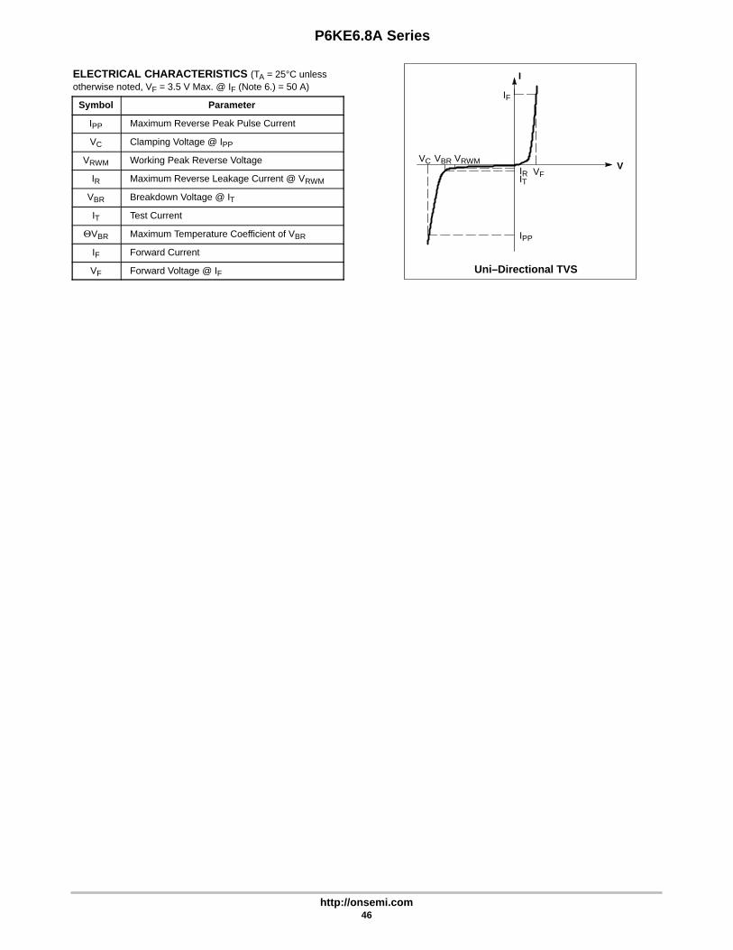
Uni–Directional TVS
IPP
IF
V
I
IRIT
VRWMVC VBRVF
P6KE6.8A Series
http://onsemi.com46
ELECTRICAL CHARACTERISTICS (TA = 25°C unlessotherwise noted, VF = 3.5 V Max. @ IF (Note 6.) = 50 A)
Symbol Parameter
IPP Maximum Reverse Peak Pulse Current
VC Clamping Voltage @ IPP
VRWM Working Peak Reverse Voltage
IR Maximum Reverse Leakage Current @ VRWM
VBR Breakdown Voltage @ IT
IT Test Current
VBR Maximum Temperature Coefficient of VBR
IF Forward Current
VF Forward Voltage @ IF

P6KE6.8A Series
http://onsemi.com47
ELECTRICAL CHARACTERISTICS (TA = 25°C unless otherwise noted, VF = 3.5 V Max. @ IF (Note 6.) = 50 A)
VRWMBreakdown Voltage VC @ IPP (Note 5.)
Device
VRWM(Note 3.) IR @ VRWM VBR (Note 4.) (Volts) @ IT VC IPP VBR
DeviceDevice
Marking Volts µA Min Nom Max mA Volts A %/°C
P6KE6.8A P6KE6.8A 5.8 1000 6.45 6.80 7.14 10 10.5 57 0.057P6KE7.5A P6KE7.5A 6.4 500 7.13 7.51 7.88 10 11.3 53 0.061P6KE8.2A P6KE8.2A 7.02 200 7.79 8.2 8.61 10 12.1 50 0.065P6KE9.1A P6KE9.1A 7.78 50 8.65 9.1 9.55 1 13.4 45 0.068
P6KE10A P6KE10A 8.55 10 9.5 10 10.5 1 14.5 41 0.073P6KE11A P6KE11A 9.4 5 10.5 11.05 11.6 1 15.6 38 0.075P6KE12A P6KE12A 10.2 5 11.4 12 12.6 1 16.7 36 0.078P6KE13A P6KE13A 11.1 5 12.4 13.05 13.7 1 18.2 33 0.081
P6KE15A P6KE15A 12.8 5 14.3 15.05 15.8 1 21.2 28 0.084P6KE16A P6KE16A 13.6 5 15.2 16 16.8 1 22.5 27 0.086P6KE18A P6KE18A 15.3 5 17.1 18 18.9 1 25.2 24 0.088P6KE20A P6KE20A 17.1 5 19 20 21 1 27.7 22 0.09
P6KE22A P6KE22A 18.8 5 20.9 22 23.1 1 30.6 20 0.092P6KE24A P6KE24A 20.5 5 22.8 24 25.2 1 33.2 18 0.094P6KE27A P6KE27A 23.1 5 25.7 27.05 28.4 1 37.5 16 0.096P6KE30A P6KE30A 25.6 5 28.5 30 31.5 1 41.4 14.4 0.097
P6KE33A P6KE33A 28.2 5 31.4 33.05 34.7 1 45.7 13.2 0.098P6KE36A P6KE36A 30.8 5 34.2 36 37.8 1 49.9 12 0.099P6KE39A P6KE39A 33.3 5 37.1 39.05 41 1 53.9 11.2 0.1P6KE43A P6KE43A 36.8 5 40.9 43.05 45.2 1 59.3 10.1 0.101
P6KE47A P6KE47A 40.2 5 44.7 47.05 49.4 1 64.8 9.3 0.101P6KE51A P6KE51A 43.6 5 48.5 51.05 53.6 1 70.1 8.6 0.102P6KE56A P6KE56A 47.8 5 53.2 56 58.8 1 77 7.8 0.103P6KE62A P6KE62A 53 5 58.9 62 65.1 1 85 7.1 0.104
P6KE68A P6KE68A 58.1 5 64.6 68 71.4 1 92 6.5 0.104P6KE75A P6KE75A 64.1 5 71.3 75.05 78.8 1 103 5.8 0.105P6KE82A P6KE82A 70.1 5 77.9 82 86.1 1 113 5.3 0.105P6KE91A P6KE91A 77.8 5 86.5 91 95.5 1 125 4.8 0.106
P6KE100A P6KE100A 85.5 5 95 100 105 1 137 4.4 0.106P6KE110A P6KE110A 94 5 105 110.5 116 1 152 4 0.107P6KE120A P6KE120A 102 5 114 120 126 1 165 3.6 0.107P6KE130A P6KE130A 111 5 124 130.5 137 1 179 3.3 0.107
P6KE150A P6KE150A 128 5 143 150.5 158 1 207 2.9 0.108P6KE160A P6KE160A 136 5 152 160 168 1 219 2.7 0.108P6KE170A P6KE170A 145 5 162 170.5 179 1 234 2.6 0.108P6KE180A P6KE180A 154 5 171 180 189 1 246 2.4 0.108P6KE200A P6KE200A 171 5 190 200 210 1 274 2.2 0.108
3. A transient suppressor is normally selected according to the maximum working peak reverse voltage (VRWM), which should be equal to orgreater than the dc or continuous peak operating voltage level.
4. VBR measured at pulse test current IT at an ambient temperature of 25°C5. Surge current waveform per Figure 4 and derate per Figures 1 and 2.
6. 1/2 sine wave (or equivalent square wave), PW = 8.3 ms, duty cycle = 4 pulses per minute maximum.

P6KE6.8A Series
http://onsemi.com48
100
10
1
0.10.1 µs 1 µs 10 µs 100 µs 1 ms 10 ms
PP
, PE
AK
PO
WE
R (
kW)
tP, PULSE WIDTH
NONREPETITIVE PULSEWAVEFORM SHOWN INFIGURE 4
Figure 1. Pulse Rating Curve
100
80
60
40
20
00 25 50 75 100 125 150 175 200
PE
AK
PU
LSE
DE
RA
TIN
G IN
% O
FP
EA
K P
OW
ER
OR
CU
RR
EN
T @
T A=
25
C
TA, AMBIENT TEMPERATURE (C)
Figure 2. Pulse Derating Curve
K
DE
RA
TIN
G F
AC
TO
R
1 ms
10 µs
10.7
0.5
0.3
0.05
0.1
0.2
0.01
0.02
0.03
0.07
100 µs
0.1 0.2 0.5 2 5 10 501 20 100D, DUTY CYCLE (%)
PULSE WIDTH10 ms
10,000
1000
100
100.1 1 10 100 1000
C, C
AP
AC
ITA
NC
E (
pF)
VBR, BREAKDOWN VOLTAGE (VOLTS)
Figure 3. Capacitance versus Breakdown Voltage
MEASURED @VRWM
MEASURED @ZERO BIAS
100
50
00 1 2 3 4
t, TIME (ms)
VA
LUE
(%
)
tr ≤ 10 µs
tP
PEAK VALUE – IPP
HALF VALUE –IPP2
Figure 4. Pulse Waveform
PULSE WIDTH (tp) ISDEFINED AS THATPOINT WHERE THEPEAK CURRENTDECAYS TO 50% OF IPP.
5
4
3
2
1
25 50 75 100 125 150 175 200
P D, S
TE
AD
Y S
TAT
E P
OW
ER
DIS
SIP
AT
ION
(W
AT
TS
)
TL, LEAD TEMPERATURE C)
3/8″
3/8″
Figure 5. Steady State Power Derating
00
Figure 6. Typical Derating Factor for Duty Cycle
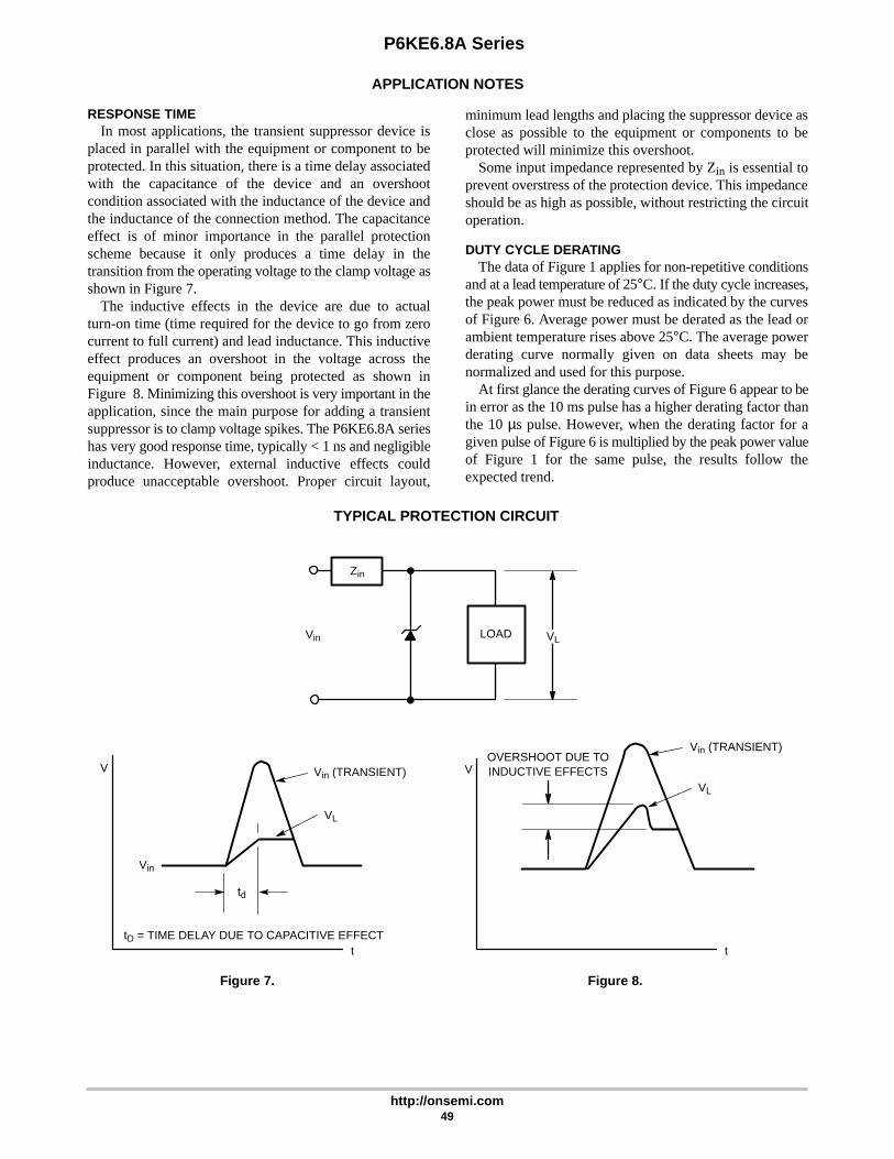
P6KE6.8A Series
http://onsemi.com49
APPLICATION NOTES
RESPONSE TIMEIn most applications, the transient suppressor device is
placed in parallel with the equipment or component to beprotected. In this situation, there is a time delay associatedwith the capacitance of the device and an overshootcondition associated with the inductance of the device andthe inductance of the connection method. The capacitanceeffect is of minor importance in the parallel protectionscheme because it only produces a time delay in thetransition from the operating voltage to the clamp voltage asshown in Figure 7.
The inductive effects in the device are due to actualturn-on time (time required for the device to go from zerocurrent to full current) and lead inductance. This inductiveeffect produces an overshoot in the voltage across theequipment or component being protected as shown inFigure 8. Minimizing this overshoot is very important in theapplication, since the main purpose for adding a transientsuppressor is to clamp voltage spikes. The P6KE6.8A serieshas very good response time, typically < 1 ns and negligibleinductance. However, external inductive effects couldproduce unacceptable overshoot. Proper circuit layout,
minimum lead lengths and placing the suppressor device asclose as possible to the equipment or components to beprotected will minimize this overshoot.
Some input impedance represented by Zin is essential toprevent overstress of the protection device. This impedanceshould be as high as possible, without restricting the circuitoperation.
DUTY CYCLE DERATINGThe data of Figure 1 applies for non-repetitive conditions
and at a lead temperature of 25°C. If the duty cycle increases,the peak power must be reduced as indicated by the curvesof Figure 6. Average power must be derated as the lead orambient temperature rises above 25°C. The average powerderating curve normally given on data sheets may benormalized and used for this purpose.
At first glance the derating curves of Figure 6 appear to bein error as the 10 ms pulse has a higher derating factor thanthe 10 µs pulse. However, when the derating factor for agiven pulse of Figure 6 is multiplied by the peak power valueof Figure 1 for the same pulse, the results follow theexpected trend.
TYPICAL PROTECTION CIRCUIT
Vin
VL
V
Vin
Vin (TRANSIENT)VL
td
V
VL
Vin (TRANSIENT)
Zin
LOAD
OVERSHOOT DUE TOINDUCTIVE EFFECTS
tD = TIME DELAY DUE TO CAPACITIVE EFFECTt t
Figure 7. Figure 8.

P6KE6.8A Series
http://onsemi.com50
UL RECOGNITION*
The entire series including the bidirectional CA suffix hasUnderwriters Laboratory Recognition for the classificationof protectors (QVGV2) under the UL standard for safety497B and File #E 116110. Many competitors only have oneor two devices recognized or have recognition in anon-protective category. Some competitors have norecognition at all. With the UL497B recognition, our partssuccessfully passed several tests including Strike Voltage
Breakdown test, Endurance Conditioning, Temperature test,Dielectric Voltage-Withstand test, Discharge test andseveral more.
Whereas, some competitors have only passed aflammability test for the package material, we have beenrecognized for much more to be included in their protectorcategory.*Applies to P6KE6.8A, CA – P6KE200A, CA.

Semiconductor Components Industries, LLC, 2001
March, 2001 – Rev. 151 Publication Order Number:
P6KE6.8CA/D
P6KE6.8CA Series
600 Watt Peak PowerSurmetic-40 Zener TransientVoltage Suppressors
Bidirectional*The P6KE6.8CA series is designed to protect voltage sensitive
components from high voltage, high energy transients. They haveexcellent clamping capability, high surge capability, low zenerimpedance and fast response t ime. These devices areON Semiconductor’s exclusive, cost-effective, highly reliableSurmetic axial leaded package and is ideally-suited for use incommunication systems, numerical controls, process controls,medical equipment, business machines, power supplies and manyother industrial/consumer applications.
Specification Features:• Working Peak Reverse Voltage Range – 5.8 to 171 V
• Peak Power – 600 Watts @ 1 ms
• ESD Rating of class 3 (>16 KV) per Human Body Model
• Maximum Clamp Voltage @ Peak Pulse Current
• Low Leakage < 5 µA above 10 V
• Maximum Temperature Coefficient Specified
• UL 497B for Isolated Loop Circuit Protection
• Response Time is Typically < 1 ns
Mechanical Characteristics:CASE: Void-free, Transfer-molded, Thermosetting plasticFINISH: All external surfaces are corrosion resistant and leads are
readily solderableMAXIMUM LEAD TEMPERATURE FOR SOLDERING PURPOSES:230°C, 1/16” from the case for 10 secondsPOLARITY: Cathode band does not imply polarityMOUNTING POSITION: Any
MAXIMUM RATINGS
Rating Symbol Value Unit
Peak Power Dissipation (Note 1.)@ TL ≤ 25°C
PPK 600 Watts
Steady State Power Dissipation@ TL ≤ 75°C, Lead Length = 3/8″Derated above TL = 75°C
PD 5
50
Watts
mW/°C
Thermal Resistance,Junction–to–Lead
RJL 15 °C/W
Operating and StorageTemperature Range
TJ, Tstg – 55 to +150 °C
1. Nonrepetitive current pulse per Figure 3 and derated above TA = 25°Cper Figure 2.
*Please see P6KE6.8A – P6KE200A for Unidirectional devices.
Device Package Shipping
ORDERING INFORMATION
P6KExxxCA Axial Lead 1000 Units/Box
AXIAL LEADCASE 17PLASTIC
http://onsemi.com
P6KExxxCARL Axial Lead 4000/Tape & Reel
L = Assembly LocationP6KExxxCA = ON Device CodeYY = YearWW = Work Week
LP6KExxxCAYYWW
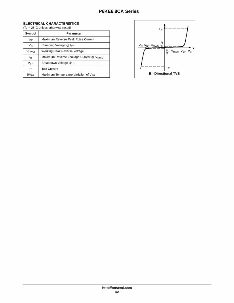
Bi–Directional TVS
IPP
IPP
V
I
IRIT
ITIRVRWMVC VBR
VRWM VCVBR
P6KE6.8CA Series
http://onsemi.com52
ELECTRICAL CHARACTERISTICS(TA = 25°C unless otherwise noted)
Symbol Parameter
IPP Maximum Reverse Peak Pulse Current
VC Clamping Voltage @ IPP
VRWM Working Peak Reverse Voltage
IR Maximum Reverse Leakage Current @ VRWM
VBR Breakdown Voltage @ IT
IT Test Current
VBR Maximum Temperature Variation of VBR

P6KE6.8CA Series
http://onsemi.com53
ELECTRICAL CHARACTERISTICS (TA = 25°C unless otherwise noted.)
VRWMBreakdown Voltage VC @ IPP (Note 4.)
Device
VRWM(Note 2.) IR @ VRWM VBR (Note 3.) (Volts) @ IT VC IPP VBR
DeviceDevice
Marking (Volts) (µA) Min Nom Max (mA) (Volts) (A) (%/°C)
P6KE6.8CA P6KE6.8CA 5.8 1000 6.45 6.80 7.14 10 10.5 57 0.057P6KE7.5CA P6KE7.5CA 6.4 500 7.13 7.51 7.88 10 11.3 53 0.061P6KE8.2CA P6KE8.2CA 7.02 200 7.79 8.2 8.61 10 12.1 50 0.065P6KE9.1CA P6KE9.1CA 7.78 50 8.65 9.1 9.55 1 13.4 45 0.068
P6KE10CA P6KE10CA 8.55 10 9.5 10 10.5 1 14.5 41 0.073P6KE11CA P6KE11CA 9.4 5 10.5 11.05 11.6 1 15.6 38 0.075P6KE12CA P6KE12CA 10.2 5 11.4 12 12.6 1 16.7 36 0.078P6KE13CA P6KE13CA 11.1 5 12.4 13.05 13.7 1 18.2 33 0.081
P6KE15CA P6KE15CA 12.8 5 14.3 15.05 15.8 1 21.2 28 0.084P6KE16CA P6KE16CA 13.6 5 15.2 16 16.8 1 22.5 27 0.086P6KE18CA P6KE18CA 15.3 5 17.1 18 18.9 1 25.2 24 0.088P6KE20CA P6KE20CA 17.1 5 19 20 21 1 27.7 22 0.09
P6KE22CA P6KE22CA 18.8 5 20.9 22 23.1 1 30.6 20 0.092P6KE24CA P6KE24CA 20.5 5 22.8 24 25.2 1 33.2 18 0.094P6KE27CA P6KE27CA 23.1 5 25.7 27.05 28.4 1 37.5 16 0.096P6KE30CA P6KE30CA 25.6 5 28.5 30 31.5 1 41.4 14.4 0.097
P6KE33CA P6KE33CA 28.2 5 31.4 33.05 34.7 1 45.7 13.2 0.098P6KE36CA P6KE36CA 30.8 5 34.2 36 37.8 1 49.9 12 0.099P6KE39CA P6KE39CA 33.3 5 37.1 39.05 41 1 53.9 11.2 0.1P6KE43CA P6KE43CA 36.8 5 40.9 43.05 45.2 1 59.3 10.1 0.101
P6KE47CA P6KE47CA 40.2 5 44.7 47.05 49.4 1 64.8 9.3 0.101P6KE51CA P6KE51CA 43.6 5 48.5 51.05 53.6 1 70.1 8.6 0.102P6KE56CA P6KE56CA 47.8 5 53.2 56 58.8 1 77 7.8 0.103P6KE62CA P6KE62CA 53 5 58.9 62 65.1 1 85 7.1 0.104
P6KE68CA P6KE68CA 58.1 5 64.6 68 71.4 1 92 6.5 0.104P6KE75CA P6KE75CA 64.1 5 71.3 75.05 78.8 1 103 5.8 0.105P6KE82CA P6KE82CA 70.1 5 77.9 82 86.1 1 113 5.3 0.105P6KE91CA P6KE91CA 77.8 5 86.5 91 95.5 1 125 4.8 0.106
P6KE100CA P6KE100CA 85.5 5 95 100 105 1 137 4.4 0.106P6KE110CA P6KE110CA 94 5 105 110.5 116 1 152 4 0.107P6KE120CA P6KE120CA 102 5 114 120 126 1 165 3.6 0.107P6KE130CA P6KE130CA 111 5 124 130.5 137 1 179 3.3 0.107
P6KE150CA P6KE150CA 128 5 143 150.5 158 1 207 2.9 0.108P6KE160CA P6KE160CA 136 5 152 160 168 1 219 2.7 0.108P6KE170CA P6KE170CA 145 5 162 170.5 179 1 234 2.6 0.108P6KE180CA P6KE180CA 154 5 171 180 189 1 246 2.4 0.108P6KE200CA P6KE200CA 171 5 190 200 210 1 274 2.2 0.108
2. A transient suppressor is normally selected according to the maximum working peak reverse voltage (VRWM), which should be equal to orgreater than the dc or continuous peak operating voltage level.
3. VBR measured at pulse test current IT at an ambient temperature of 25°C.4. Surge current waveform per Figure 3 and derate per Figures 1 and 2.

P6KE6.8CA Series
http://onsemi.com54
100
10
1
0.10.1 s 1 s 10 s 100 s 1 s 10 s
PP
, PE
AK
PO
WE
R (
kW)
tP, PULSE WIDTH
NONREPETITIVEPULSE WAVEFORMSHOWN IN FIGURE 3
Figure 1. Pulse Rating Curve
100
80
60
40
20
00 25 50 75 100 125 150 175 200
PE
AK
PU
LSE
DE
RA
TIN
G IN
% O
FP
EA
K P
OW
ER
OR
CU
RR
EN
T @
TA=
25
C
TA, AMBIENT TEMPERATURE (°C)
Figure 2. Pulse Derating Curve
K°
DE
RA
TIN
G F
AC
TO
R
1 ms
10 s
10.7
0.5
0.3
0.05
0.1
0.2
0.01
0.02
0.03
0.07
100 s
0.1 0.2 0.5 2 5 10 501 20 100D, DUTY CYCLE (%)
PULSE WIDTH10 ms
100
50
00 1 2 3 4
t, TIME (ms)
VA
LUE
(%
)
tP
PEAK VALUE – IPP
HALF VALUE –IPP2
Figure 3. Pulse Waveform
PULSE WIDTH (tp) ISDEFINED AS THATPOINT WHERE THEPEAK CURRENTDECAYS TO 50% OF IPP.
5
4
3
2
1
25 50 75 100 125 150 175 200
P D, S
TE
AD
Y S
TAT
E P
OW
ER
DIS
SIP
AT
ION
(W
AT
TS
)
TL, LEAD TEMPERATURE (°C)
3/8,
3/8,
Figure 4. Steady State Power Derating
00
Figure 5. Typical Derating Factor for Duty Cycle
tr ≤ 10 s

P6KE6.8CA Series
http://onsemi.com55
APPLICATION NOTES
RESPONSE TIMEIn most applications, the transient suppressor device is
placed in parallel with the equipment or component to beprotected. In this situation, there is a time delay associatedwith the capacitance of the device and an overshootcondition associated with the inductance of the device andthe inductance of the connection method. The capacitanceeffect is of minor importance in the parallel protectionscheme because it only produces a time delay in thetransition from the operating voltage to the clamp voltage asshown in Figure 6.
The inductive effects in the device are due to actualturn-on time (time required for the device to go from zerocurrent to full current) and lead inductance. This inductiveeffect produces an overshoot in the voltage across theequipment or component being protected as shown inFigure 7. Minimizing this overshoot is very important in theapplication, since the main purpose for adding a transientsuppressor is to clamp voltage spikes. The P6KE6.8A serieshas very good response time, typically < 1 ns and negligibleinductance. However, external inductive effects couldproduce unacceptable overshoot. Proper circuit layout,
minimum lead lengths and placing the suppressor device asclose as possible to the equipment or components to beprotected will minimize this overshoot.
Some input impedance represented by Zin is essential toprevent overstress of the protection device. This impedanceshould be as high as possible, without restricting the circuitoperation.
DUTY CYCLE DERATINGThe data of Figure 1 applies for non-repetitive conditions
and at a lead temperature of 25°C. If the duty cycle increases,the peak power must be reduced as indicated by the curvesof Figure 5. Average power must be derated as the lead orambient temperature rises above 25°C. The average powerderating curve normally given on data sheets may benormalized and used for this purpose.
At first glance the derating curves of Figure 5 appear to bein error as the 10 ms pulse has a higher derating factor thanthe 10 µs pulse. However, when the derating factor for agiven pulse of Figure 5 is multiplied by the peak power valueof Figure 1 for the same pulse, the results follow theexpected trend.
TYPICAL PROTECTION CIRCUIT
Vin
VL
V
Vin
Vin (TRANSIENT)VL
td
V
VL
Vin (TRANSIENT)
Zin
LOAD
OVERSHOOT DUE TOINDUCTIVE EFFECTS
tD = TIME DELAY DUE TO CAPACITIVE EFFECTt t
Figure 6. Figure 7.

P6KE6.8CA Series
http://onsemi.com56
UL RECOGNITION*
The entire series including the bidirectional CA suffix hasUnderwriters Laboratory Recognition for the classificationof protectors (QVGV2) under the UL standard for safety497B and File #E 116110. Many competitors only have oneor two devices recognized or have recognition in anon-protective category. Some competitors have norecognition at all. With the UL497B recognition, our partssuccessfully passed several tests including Strike Voltage
Breakdown test, Endurance Conditioning, Temperature test,Dielectric Voltage-Withstand test, Discharge test andseveral more.
Whereas, some competitors have only passed aflammability test for the package material, we have beenrecognized for much more to be included in their protectorcategory.*Applies to P6KE6.8A, CA – P6KE200A, CA.
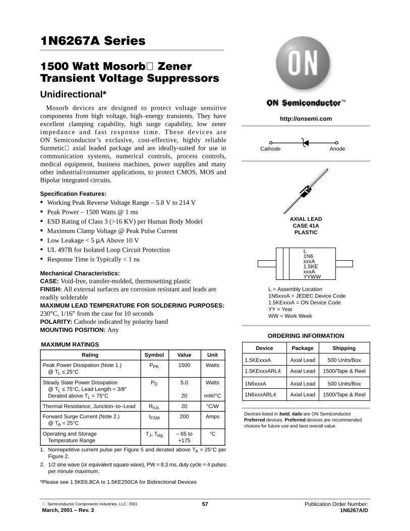
Semiconductor Components Industries, LLC, 2001
March, 2001 – Rev. 357 Publication Order Number:
1N6267A/D
1N6267A Series
1500 Watt Mosorb ZenerTransient Voltage Suppressors
Unidirectional*Mosorb devices are designed to protect voltage sensitive
components from high voltage, high–energy transients. They haveexcellent clamping capability, high surge capability, low zenerimpedance and fast response t ime. These devices areON Semiconductor’s exclusive, cost-effective, highly reliableSurmetic axial leaded package and are ideally-suited for use incommunication systems, numerical controls, process controls,medical equipment, business machines, power supplies and manyother industrial/consumer applications, to protect CMOS, MOS andBipolar integrated circuits.
Specification Features:• Working Peak Reverse Voltage Range – 5.8 V to 214 V
• Peak Power – 1500 Watts @ 1 ms
• ESD Rating of Class 3 (>16 KV) per Human Body Model
• Maximum Clamp Voltage @ Peak Pulse Current
• Low Leakage < 5 µA Above 10 V
• UL 497B for Isolated Loop Circuit Protection
• Response Time is Typically < 1 ns
Mechanical Characteristics:CASE: Void-free, transfer-molded, thermosetting plasticFINISH: All external surfaces are corrosion resistant and leads arereadily solderableMAXIMUM LEAD TEMPERATURE FOR SOLDERING PURPOSES:230°C, 1/16″ from the case for 10 secondsPOLARITY: Cathode indicated by polarity bandMOUNTING POSITION: Any
MAXIMUM RATINGS
Rating Symbol Value Unit
Peak Power Dissipation (Note 1.)@ TL ≤ 25°C
PPK 1500 Watts
Steady State Power Dissipation@ TL ≤ 75°C, Lead Length = 3/8″Derated above TL = 75°C
PD 5.0
20
Watts
mW/°C
Thermal Resistance, Junction–to–Lead RJL 20 °C/W
Forward Surge Current (Note 2.)@ TA = 25°C
IFSM 200 Amps
Operating and StorageTemperature Range
TJ, Tstg – 65 to+175
°C
1. Nonrepetitive current pulse per Figure 5 and derated above TA = 25°C perFigure 2.
2. 1/2 sine wave (or equivalent square wave), PW = 8.3 ms, duty cycle = 4 pulsesper minute maximum.
*Please see 1.5KE6.8CA to 1.5KE250CA for Bidirectional Devices
Devices listed in bold, italic are ON SemiconductorPreferred devices. Preferred devices are recommendedchoices for future use and best overall value.
AXIAL LEADCASE 41APLASTIC
http://onsemi.com
L = Assembly Location1N6xxxA = JEDEC Device Code1.5KExxxA = ON Device CodeYY = YearWW = Work Week
Cathode Anode
Device Package Shipping
ORDERING INFORMATION
1.5KExxxA Axial Lead 500 Units/Box
1.5KExxxARL4 Axial Lead 1500/Tape & Reel
1N6xxxA Axial Lead 500 Units/Box
1N6xxxARL4 Axial Lead 1500/Tape & Reel
L1N6xxxA1.5KExxxAYYWW

Uni–Directional TVS
IPP
IF
V
I
IRIT
VRWMVC VBRVF
1N6267A Series
http://onsemi.com58
ELECTRICAL CHARACTERISTICS (TA = 25°C unlessotherwise noted, VF = 3.5 V Max., IF (Note 3.) = 100 A)
Symbol Parameter
IPP Maximum Reverse Peak Pulse Current
VC Clamping Voltage @ IPP
VRWM Working Peak Reverse Voltage
IR Maximum Reverse Leakage Current @ VRWM
VBR Breakdown Voltage @ IT
IT Test Current
VBR Maximum Temperature Coefficient of VBR
IF Forward Current
VF Forward Voltage @ IF

1N6267A Series
http://onsemi.com59
ELECTRICAL CHARACTERISTICS (TA = 25°C unless otherwise noted, VF = 3.5 V Max. @ IF (Note 3.) = 100 A)
VRWMBreakdown Voltage VC @ IPP (Note 7.)
JEDECDevice
VRWM(Note 5.) IR @ VRWM VBR (Note 6.) (Volts) @ IT VC IPP VBR
DeviceDevice
(Note 4.) (Volts) (µA) Min Nom Max (mA) (Volts) (A) (%/°C)
1.5KE6.8A 1N6267A 5.8 1000 6.45 6.8 7.14 10 10.5 143 0.0571.5KE7.5A 1N6268A 6.4 500 7.13 7.5 7.88 10 11.3 132 0.0611.5KE8.2A 1N6269A 7.02 200 7.79 8.2 8.61 10 12.1 124 0.0651.5KE9.1A 1N6270A 7.78 50 8.65 9.1 9.55 1 13.4 112 0.068
1.5KE10A 1N6271A 8.55 10 9.5 10 10.5 1 14.5 103 0.0731.5KE11A 1N6272A 9.4 5 10.5 11 11.6 1 15.6 96 0.0751.5KE12A 1N6273A 10.2 5 11.4 12 12.6 1 16.7 90 0.0781.5KE13A 1N6274A 11.1 5 12.4 13 13.7 1 18.2 82 0.081
1.5KE15A 1N6275A 12.8 5 14.3 15 15.8 1 21.2 71 0.0841.5KE16A 1N6276A 13.6 5 15.2 16 16.8 1 22.5 67 0.0861.5KE18A 1N6277A 15.3 5 17.1 18 18.9 1 25.2 59.5 0.0881.5KE20A 1N6278A 17.1 5 19 20 21 1 27.7 54 0.09
1.5KE22A 1N6279A 18.8 5 20.9 22 23.1 1 30.6 49 0.0921.5KE24A 1N6280A 20.5 5 22.8 24 25.2 1 33.2 45 0.0941.5KE27A 1N6281A 23.1 5 25.7 27 28.4 1 37.5 40 0.0961.5KE30A 1N6282A 25.6 5 28.5 30 31.5 1 41.4 36 0.097
1.5KE33A 1N6283A 28.2 5 31.4 33 34.7 1 45.7 33 0.0981.5KE36A 1N6284A 30.8 5 34.2 36 37.8 1 49.9 30 0.0991.5KE39A 1N6285A 33.3 5 37.1 39 41 1 53.9 28 0.11.5KE43A 1N6286A 36.8 5 40.9 43 45.2 1 59.3 25.3 0.101
1.5KE47A 1N6287A 40.2 5 44.7 47 49.4 1 64.8 23.2 0.1011.5KE51A 1N6288A 43.6 5 48.5 51 53.6 1 70.1 21.4 0.1021.5KE56A 1N6289 47.8 5 53.2 56 58.8 1 77 19.5 0.1031.5KE62A 1N6290A 53 5 58.9 62 65.1 1 85 17.7 0.104
1.5KE68A 1N6291A 58.1 5 64.6 68 71.4 1 92 16.3 0.1041.5KE75A 1N6292A 64.1 5 71.3 75 78.8 1 103 14.6 0.1051.5KE82A 1N6293A 70.1 5 77.9 82 86.1 1 113 13.3 0.1051.5KE91A 1N6294A 77.8 5 86.5 91 95.5 1 125 12 0.106
1.5KE100A 1N6295A 85.5 5 95 100 105 1 137 11 0.1061.5KE110A 1N6296A 94 5 105 110 116 1 152 9.9 0.1071.5KE120A 1N6297A 102 5 114 120 126 1 165 9.1 0.1071.5KE130A 1N6298A 111 5 124 130 137 1 179 8.4 0.107
1.5KE150A 1N6299A 128 5 143 150 158 1 207 7.2 0.1081.5KE160A 1N6300A 136 5 152 160 168 1 219 6.8 0.1081.5KE170A 1N6301A 145 5 162 170 179 1 234 6.4 0.1081.5KE180A 1N6302A 154 5 171 180 189 1 246 6.1 0.108
1.5KE200A 1N6303A 171 5 190 200 210 1 274 5.5 0.1081.5KE220A 185 5 209 220 231 1 328 4.6 0.1091.5KE250A 214 5 237 250 263 1 344 5 0.109
3. 1/2 sine wave (or equivalent square wave), PW = 8.3 ms, duty cycle = 4 pulses per minute maximum.4. Indicates JEDEC registered data5. A transient suppressor is normally selected according to the maximum working peak reverse voltage (VRWM), which should be equal to or
greater than the dc or continuous peak operating voltage level.6. VBR measured at pulse test current IT at an ambient temperature of 25°C7. Surge current waveform per Figure 5 and derate per Figures 1 and 2.

1N6267A Series
http://onsemi.com60
Figure 1. Pulse Rating Curve
100
80
60
40
20
00 25 50 75 100 125 150 175 200
PE
AK
PU
LSE
DE
RAT
ING
IN %
OF
PE
AK
PO
WE
R O
R C
UR
RE
NT
@ T
A=
25C°
TA, AMBIENT TEMPERATURE (°C)
Figure 2. Pulse Derating Curve
5
4
3
2
1
25 50 75 100 125 150 175 200
P D, S
TE
AD
Y S
TAT
E P
OW
ER
DIS
SIP
AT
ION
(W
AT
TS
)
TL, LEAD TEMPERATURE (°C)
3/8″
3/8″
00
100
50
00 1 2 3 4
t, TIME (ms)
, VA
LUE
(%
)
tr
tP
PEAK VALUE - IPP
HALF VALUE -IPP
2
PULSE WIDTH (tP) IS DEFINED ASTHAT POINT WHERE THE PEAKCURRENT DECAYS TO 50% OF IPP.tr ≤ 10µs
1µs 10µs 100µs 1 ms 10 ms
100
10
1
tP, PULSE WIDTH
PP
K, P
EA
K P
OW
ER
(kW
)NONREPETITIVEPULSE WAVEFORMSHOWN IN FIGURE 5
0.1µs
I PP
Figure 3. Capacitance versus Breakdown Voltage
1N6267A/1.5KE6.8Athrough
1N6303A/1.5KE200A
VBR, BREAKDOWN VOLTAGE (VOLTS)
1 10 100 1000
10,000
1000
100
10
C, C
APA
CIT
AN
CE
(pF
)
MEASURED @ VRWM
MEASURED @ZERO BIAS
Figure 4. Steady State Power Derating Figure 5. Pulse Waveform
1N6373, ICTE-5, MPTE-5,through
1N6389, ICTE-45, C, MPTE-45, C
VBR, BREAKDOWN VOLTAGE (VOLTS)
1 10 100 1000
10,000
1000
100
10
C, C
APA
CIT
AN
CE
(pF
)
MEASURED @ZERO BIAS
MEASURED @ VRWM

1N6267A Series
http://onsemi.com61
1N6373, ICTE-5, MPTE-5,through
1N6389, ICTE-45, C, MPTE-45, C
1.5KE6.8CAthrough
1.5KE200CA
Figure 6. Dynamic Impedance
1000
500
200
100
50
20
10
5
2
1
1000
500
200
100
50
20
10
5
2
10.3 0.5 0.7 1 2 3 5 7 10 20 30
∆VBR, INSTANTANEOUS INCREASE IN VBR ABOVE VBR(NOM) (VOLTS)
0.3 0.5 0.7 1 2 3 5 7 10 20 30
∆VBR, INSTANTANEOUS INCREASE IN VBR ABOVE VBR(NOM) (VOLTS)
I T, T
ES
T C
UR
RE
NT
(AM
PS
)
VBR(NOM)=6.8 to 13VTL=25°CtP=10µs
VBR(NOM)=6.8 to 13V
20V24V 43V
75V
180V
120V
20V24V 43V
Figure 7. Typical Derating Factor for Duty Cycle
DE
RAT
ING
FA
CT
OR
1 ms
10 µs
1
0.7
0.5
0.3
0.05
0.1
0.2
0.01
0.02
0.03
0.07
100 µs
0.1 0.2 0.5 2 5 10 501 20 100
D, DUTY CYCLE (%)
PULSE WIDTH10 ms
TL=25°CtP=10µs
I T, T
ES
T C
UR
RE
NT
(AM
PS
)
APPLICATION NOTES
RESPONSE TIME
In most applications, the transient suppressor device isplaced in parallel with the equipment or component to beprotected. In this situation, there is a time delay associatedwith the capacitance of the device and an overshootcondition associated with the inductance of the device andthe inductance of the connection method. The capacitanceeffect is of minor importance in the parallel protectionscheme because it only produces a time delay in thetransition from the operating voltage to the clamp voltage asshown in Figure 8.
The inductive effects in the device are due to actualturn-on time (time required for the device to go from zerocurrent to full current) and lead inductance. This inductiveeffect produces an overshoot in the voltage across theequipment or component being protected as shown inFigure 9. Minimizing this overshoot is very important in the
application, since the main purpose for adding a transientsuppressor is to clamp voltage spikes. These devices haveexcellent response time, typically in the picosecond rangeand negligible inductance. However, external inductiveeffects could produce unacceptable overshoot. Propercircuit layout, minimum lead lengths and placing thesuppressor device as close as possible to the equipment orcomponents to be protected will minimize this overshoot.
Some input impedance represented by Zin is essential toprevent overstress of the protection device. This impedanceshould be as high as possible, without restricting the circuitoperation.
DUTY CYCLE DERATINGThe data of Figure 1 applies for non-repetitive conditions
and at a lead temperature of 25°C. If the duty cycle increases,the peak power must be reduced as indicated by the curvesof Figure 7. Average power must be derated as the lead or
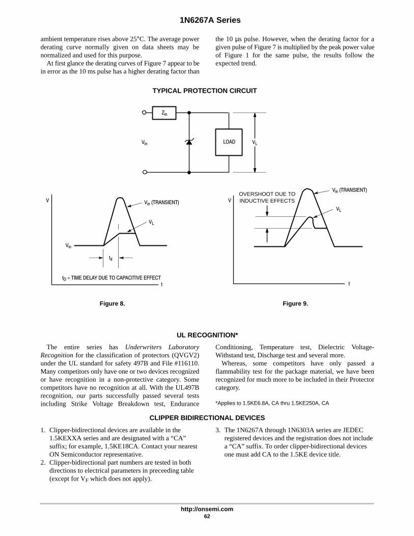
1N6267A Series
http://onsemi.com62
ambient temperature rises above 25°C. The average powerderating curve normally given on data sheets may benormalized and used for this purpose.
At first glance the derating curves of Figure 7 appear to bein error as the 10 ms pulse has a higher derating factor than
the 10 µs pulse. However, when the derating factor for agiven pulse of Figure 7 is multiplied by the peak power valueof Figure 1 for the same pulse, the results follow theexpected trend.
TYPICAL PROTECTION CIRCUIT
Vin
VL
V
Vin
Vin (TRANSIENT)VL
td
V
VL
Vin (TRANSIENT)
Zin
LOAD
OVERSHOOT DUE TOINDUCTIVE EFFECTS
tD = TIME DELAY DUE TO CAPACITIVE EFFECTt t
Figure 8. Figure 9.
UL RECOGNITION*
The entire series has Underwriters LaboratoryRecognition for the classification of protectors (QVGV2)under the UL standard for safety 497B and File #116110.Many competitors only have one or two devices recognizedor have recognition in a non-protective category. Somecompetitors have no recognition at all. With the UL497Brecognition, our parts successfully passed several testsincluding Strike Voltage Breakdown test, Endurance
Conditioning, Temperature test, Dielectric Voltage-Withstand test, Discharge test and several more.
Whereas, some competitors have only passed aflammability test for the package material, we have beenrecognized for much more to be included in their Protectorcategory.
*Applies to 1.5KE6.8A, CA thru 1.5KE250A, CA
CLIPPER BIDIRECTIONAL DEVICES
1. Clipper-bidirectional devices are available in the1.5KEXXA series and are designated with a “CA”suffix; for example, 1.5KE18CA. Contact your nearestON Semiconductor representative.
2. Clipper-bidirectional part numbers are tested in bothdirections to electrical parameters in preceeding table(except for VF which does not apply).
3. The 1N6267A through 1N6303A series are JEDECregistered devices and the registration does not includea “CA” suffix. To order clipper-bidirectional devicesone must add CA to the 1.5KE device title.

Semiconductor Components Industries, LLC, 2001
March, 2001 – Rev. 563 Publication Order Number:
SA5.0A/D
SA5.0A Series
500 Watt Peak PowerMiniMOSORB Zener TransientVoltage Suppressors
Unidirectional*The SA5.0A series is designed to protect voltage sensitive
components from high voltage, high energy transients. They haveexcellent clamping capability, high surge capability, low zenerimpedance and fast response time. The SA5.0A series is supplied inON Semiconductor’s exclusive, cost-effective, highly reliableSurmetic axial leaded package and is ideally-suited for use incommunication systems, numerical controls, process controls,medical equipment, business machines, power supplies and manyother industrial/consumer applications.
Specification Features:• Working Peak Reverse Voltage Range – 5 to 170 V
• Peak Power – 500 Watts @ 1 ms
• ESD Rating of Class 3 (>16 KV) per Human Body Model
• Maximum Clamp Voltage @ Peak Pulse Current
• Low Leakage < 1 µA above 8.5 V
• UL 497B for Isolated Loop Circuit Protection
• Maximum Temperature Coefficient Specified
• Response Time is typically < 1 ns
Mechanical Characteristics:CASE: Void-free, Transfer-molded, Thermosetting plasticFINISH: All external surfaces are corrosion resistant and leads are
readily solderableMAXIMUM LEAD TEMPERATURE FOR SOLDERING: 230C,
1/16″ from the case for 10 secondsPOLARITY: Cathode indicated by polarity band.MOUNTING POSITION: Any
MAXIMUM RATINGS
Rating Symbol Value Unit
Peak Power Dissipation (Note 1.)@ TL ≤ 25°C
PPK 500 Watts
Steady State Power Dissipation@ TL ≤ 75°C, Lead Length = 3/8″Derated above TL = 75°C
PD 3.0
30
Watts
mW/°C
Thermal Resistance, Junction–to–Lead RJL 33.3 °C/W
Forward Surge Current (Note 2.)@ TA = 25°C
IFSM 70 Amps
Operating and Storage TemperatureRange
TJ, Tstg – 55 to+175
°C
1. Nonrepetitive current pulse per Figure 4 and derated above TA = 25°C perFigure 2.
2. 1/2 sine wave (or equivalent square wave), PW = 8.3 ms, duty cycle = 4 pulsesper minute
*Please see SA5.0CA – SA170CA for Bidirectional devices.
Device Package Shipping
ORDERING INFORMATION
SAxxxA Axial Lead 1000 Units/Box
http://onsemi.com
SAxxxARL Axial Lead 5000/Tape & Reel
AXIAL LEADCASE 59PLASTIC
L = Assembly LocationSAxxxA = ON Device CodeYY = YearWW = Work Week
LSAxxxAYYWW
Cathode Anode
Devices listed in bold, italic are ON SemiconductorPreferred devices. Preferred devices are recommendedchoices for future use and best overall value.

Uni–Directional TVS
IPP
IF
V
I
IRIT
VRWMVC VBRVF
SA5.0A Series
http://onsemi.com64
ELECTRICAL CHARACTERISTICS (TA = 25°C unlessotherwise noted, VF = 3.5 V Max. @ IF (Note 6.) = 35 A)
Symbol Parameter
IPP Maximum Reverse Peak Pulse Current
VC Clamping Voltage @ IPP
VRWM Working Peak Reverse Voltage
IR Maximum Reverse Leakage Current @ VRWM
VBR Breakdown Voltage @ IT
IT Test Current
VBR Maximum Temperature Variation of VBR
IF Forward Current
VF Forward Voltage @ IF
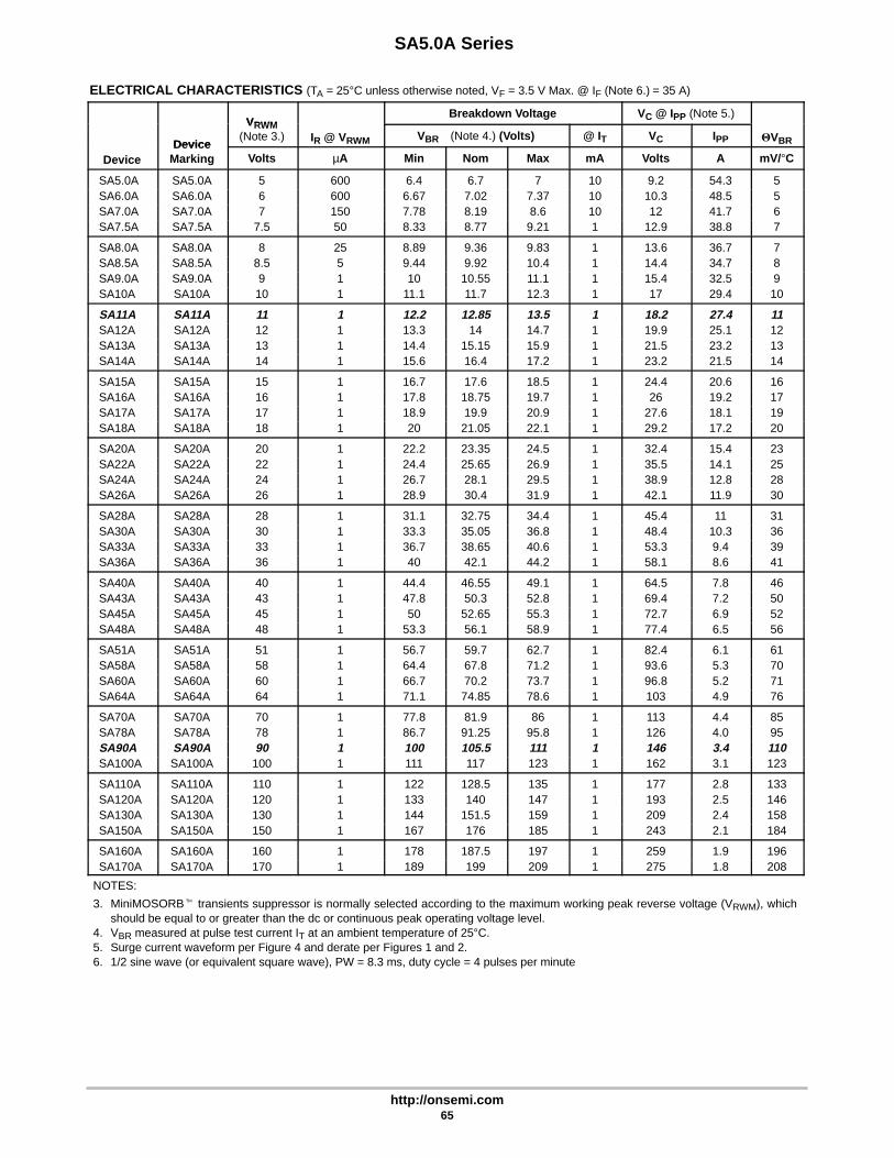
SA5.0A Series
http://onsemi.com65
ELECTRICAL CHARACTERISTICS (TA = 25°C unless otherwise noted, VF = 3.5 V Max. @ IF (Note 6.) = 35 A)
VRWMBreakdown Voltage VC @ IPP (Note 5.)
Device
VRWM(Note 3.) IR @ VRWM VBR (Note 4.) (Volts) @ IT VC IPP VBR
DeviceDevice
Marking Volts µA Min Nom Max mA Volts A mV/°C
SA5.0A SA5.0A 5 600 6.4 6.7 7 10 9.2 54.3 5SA6.0A SA6.0A 6 600 6.67 7.02 7.37 10 10.3 48.5 5SA7.0A SA7.0A 7 150 7.78 8.19 8.6 10 12 41.7 6SA7.5A SA7.5A 7.5 50 8.33 8.77 9.21 1 12.9 38.8 7
SA8.0A SA8.0A 8 25 8.89 9.36 9.83 1 13.6 36.7 7SA8.5A SA8.5A 8.5 5 9.44 9.92 10.4 1 14.4 34.7 8SA9.0A SA9.0A 9 1 10 10.55 11.1 1 15.4 32.5 9SA10A SA10A 10 1 11.1 11.7 12.3 1 17 29.4 10
SA11A SA11A 11 1 12.2 12.85 13.5 1 18.2 27.4 11SA12A SA12A 12 1 13.3 14 14.7 1 19.9 25.1 12SA13A SA13A 13 1 14.4 15.15 15.9 1 21.5 23.2 13SA14A SA14A 14 1 15.6 16.4 17.2 1 23.2 21.5 14
SA15A SA15A 15 1 16.7 17.6 18.5 1 24.4 20.6 16SA16A SA16A 16 1 17.8 18.75 19.7 1 26 19.2 17SA17A SA17A 17 1 18.9 19.9 20.9 1 27.6 18.1 19SA18A SA18A 18 1 20 21.05 22.1 1 29.2 17.2 20
SA20A SA20A 20 1 22.2 23.35 24.5 1 32.4 15.4 23SA22A SA22A 22 1 24.4 25.65 26.9 1 35.5 14.1 25SA24A SA24A 24 1 26.7 28.1 29.5 1 38.9 12.8 28SA26A SA26A 26 1 28.9 30.4 31.9 1 42.1 11.9 30
SA28A SA28A 28 1 31.1 32.75 34.4 1 45.4 11 31SA30A SA30A 30 1 33.3 35.05 36.8 1 48.4 10.3 36SA33A SA33A 33 1 36.7 38.65 40.6 1 53.3 9.4 39SA36A SA36A 36 1 40 42.1 44.2 1 58.1 8.6 41
SA40A SA40A 40 1 44.4 46.55 49.1 1 64.5 7.8 46SA43A SA43A 43 1 47.8 50.3 52.8 1 69.4 7.2 50SA45A SA45A 45 1 50 52.65 55.3 1 72.7 6.9 52SA48A SA48A 48 1 53.3 56.1 58.9 1 77.4 6.5 56
SA51A SA51A 51 1 56.7 59.7 62.7 1 82.4 6.1 61SA58A SA58A 58 1 64.4 67.8 71.2 1 93.6 5.3 70SA60A SA60A 60 1 66.7 70.2 73.7 1 96.8 5.2 71SA64A SA64A 64 1 71.1 74.85 78.6 1 103 4.9 76
SA70A SA70A 70 1 77.8 81.9 86 1 113 4.4 85SA78A SA78A 78 1 86.7 91.25 95.8 1 126 4.0 95SA90A SA90A 90 1 100 105.5 111 1 146 3.4 110SA100A SA100A 100 1 111 117 123 1 162 3.1 123
SA110A SA110A 110 1 122 128.5 135 1 177 2.8 133SA120A SA120A 120 1 133 140 147 1 193 2.5 146SA130A SA130A 130 1 144 151.5 159 1 209 2.4 158SA150A SA150A 150 1 167 176 185 1 243 2.1 184
SA160A SA160A 160 1 178 187.5 197 1 259 1.9 196SA170A SA170A 170 1 189 199 209 1 275 1.8 208
NOTES:
3. MiniMOSORB transients suppressor is normally selected according to the maximum working peak reverse voltage (VRWM), whichshould be equal to or greater than the dc or continuous peak operating voltage level.
4. VBR measured at pulse test current IT at an ambient temperature of 25°C.5. Surge current waveform per Figure 4 and derate per Figures 1 and 2.6. 1/2 sine wave (or equivalent square wave), PW = 8.3 ms, duty cycle = 4 pulses per minute
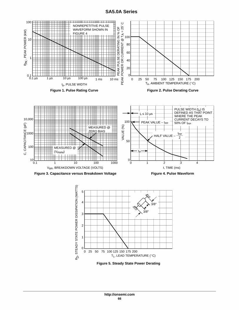
SA5.0A Series
http://onsemi.com66
100
10
1
0.10.1 µs 1 µs 10 µs 100 µs 1 ms 10 ms
P P, P
EA
K P
OW
ER
(kW
)
tp, PULSE WIDTH
Figure 1. Pulse Rating Curve
NONREPETITIVE PULSEWAVEFORM SHOWN INFIGURE 4
100
80
60
40
20
00 25 50 75 100 125 150 175 200
PE
AK
PU
LSE
DE
RA
TIN
G IN
% O
FP
EA
K P
OW
ER
OR
CU
RR
EN
T @
TA
= 2
5C
TA, AMBIENT TEMPERATURE (C)
Figure 2. Pulse Derating Curve
10,000
1000
100
100.1 1 10 100 1000
C, C
AP
AC
ITA
NC
E (
pF)
VBR, BREAKDOWN VOLTAGE (VOLTS)
MEASURED @ZERO BIAS
Figure 3. Capacitance versus Breakdown Voltage
100
50
00 1 2 3 4
t, TIME (ms)
VA
LUE
(%
)
PULSE WIDTH (tp) ISDEFINED AS THAT POINTWHERE THE PEAKCURRENT DECAYS TO50% OF IPP.PEAK VALUE – IPP
HALF VALUE –IPP2
Figure 4. Pulse Waveform
5
4
3
2
1
00 25 50 75 100 125 150 175 200
P D, S
TE
AD
Y S
TAT
E P
OW
ER
DIS
SIP
AT
ION
(W
AT
TS
)
TL, LEAD TEMPERATURE (C)
3/8″
3/8″
Figure 5. Steady State Power Derating
tr ≤ 10 µs
MEASURED @(VRWM) tP
K

SA5.0A Series
http://onsemi.com67
UL RECOGNITION*
The entire series including the bidirectional CA suffix hasUnderwriters Laboratory Recognition for the classificationof protectors (QVGV2) under the UL standard for safety497B and File #E 116110. Many competitors only have oneor two devices recognized or have recognition in anon-protective category. Some competitors have norecognition at all. With the UL497B recognition, our partssuccessfully passed several tests including Strike Voltage
Breakdown test, Endurance Conditioning, Temperature test,Dielectric Voltage-Withstand test, Discharge test andseveral more.
Whereas, some competitors have only passed aflammability test for the package material, we have beenrecognized for much more to be included in their protectorcategory.*Applies to SA5.0A, CA – SA170A, CA.

Semiconductor Components Industries, LLC, 2001
March, 2001 – Rev. 168 Publication Order Number:
SA5.0CA/D
SA5.0CA Series
500 Watt Peak PowerMiniMOSORB Zener TransientVoltage Suppressors
Bidirectional*The SA5.0CA series is designed to protect voltage sensitive
components from high voltage, high–energy transients. They haveexcellent clamping capability, high surge capability, low zenerimpedance and fast response time. The SA5.0CA series is supplied inON Semiconductor’s exclusive, cost-effective, highly reliableSurmetic axial leaded package and is ideally-suited for use incommunication systems, numerical controls, process controls,medical equipment, business machines, power supplies and manyother industrial/consumer applications.
Specification Features:• Working Peak Reverse Voltage Range – 5.0 to 170 V
• Peak Power – 500 Watts @ 1 ms
• ESD Rating of Class 3 (>16 KV) per Human Body Model
• Maximum Clamp Voltage @ Peak Pulse Current
• Low Leakage < 1 µA above 8.5 V
• UL 497B for Isolated Loop Circuit Protection
• Maximum Temperature Coefficient Specified
• Response Time is typically < 1 ns
Mechanical Characteristics:CASE: Void-free, Transfer-molded, Thermosetting plasticFINISH: All external surfaces are corrosion resistant and leads are
readily solderableMAXIMUM LEAD TEMPERATURE FOR SOLDERING PURPOSES:230°C, 1/16″ from the case for 10 secondsPOLARITY: Cathode band does not imply polarityMOUNTING POSITION: Any
MAXIMUM RATINGS
Rating Symbol Value Unit
Peak Power Dissipation (Note 1.)@ TL ≤ 25°C
PPK 500 Watts
Steady State Power Dissipation @TL ≤ 75°C, Lead Length = 3/8″Derated above TL = 75°C
PD 3.0
30
Watts
mW/°C
Thermal Resistance,Junction–to–Lead
RJL 33.3 °C/W
Operating and Storage TemperatureRange
TJ, Tstg – 55 to +175 °C
1. Nonrepetitive current pulse per Figure 3 and derated above TA = 25°Cper Figure 2.
*Please see SA5.0A to SA170A for Unidirectional devices.
Device Package Shipping
ORDERING INFORMATION
AXIAL LEADCASE 59PLASTIC
http://onsemi.com
SAxxxCA Axial Lead 1000 Units/Box
SAxxxCARL Axial Lead 5000/Tape & Reel
L = Assembly LocationSAxxxCA = ON Device CodeYY = YearWW = Work Week
LSAxxxCAYYWW
Devices listed in bold, italic are ON SemiconductorPreferred devices. Preferred devices are recommendedchoices for future use and best overall value.

Bi–Directional TVS
IPP
IPP
V
I
IRIT
ITIRVRWMVC VBR
VRWM VCVBR
SA5.0CA Series
http://onsemi.com69
ELECTRICAL CHARACTERISTICS(TA = 25°C unless otherwise noted)
Symbol Parameter
IPP Maximum Reverse Peak Pulse Current
VC Clamping Voltage @ IPP
VRWM Working Peak Reverse Voltage
IR Maximum Reverse Leakage Current @ VRWM
VBR Breakdown Voltage @ IT
IT Test Current
VBR Maximum Temperature Variation of VBR
ELECTRICAL CHARACTERISTICS (TA = 25°C unless otherwise noted.)
VRWMBreakdown Voltage VC @ IPP (Note 4.)
Device
VRWM(Note 2.) IR @ VRWM VBR (Note 3.) (Volts) @ IT VC IPP VBR
DeviceDevice
Marking (Volts) (µA) Min Nom Max (mA) (Volts) (A) (mV/°C)
SA5.0CA SA5.0CA 5 600 6.4 6.7 7 10 9.2 54.3 5SA6.0CA SA6.0CA 6 600 6.67 7.02 7.37 10 10.3 48.5 5SA6.5CA SA6.5CA 6.5 400 7.22 7.60 7.98 10 11.2 44.7 5SA7.0CA SA7.0CA 7 150 7.78 8.19 8.6 10 12 41.7 6
SA7.5CA SA7.5CA 7.5 50 8.33 8.77 9.21 1 12.9 38.8 7SA8.0CA SA8.0CA 8 25 8.89 9.36 9.83 1 13.6 36.7 7SA8.5CA SA8.5CA 8.5 5 9.44 9.92 10.4 1 14.4 34.7 8SA9.0CA SA9.0CA 9 1 10 10.55 11.1 1 15.4 32.5 9
SA10CA SA10CA 10 1 11.1 11.7 12.3 1 17 29.4 10SA11CA SA11CA 11 1 12.2 12.85 13.5 1 18.2 27.4 11SA12CA SA12CA 12 1 13.3 14 14.7 1 19.9 25.1 12SA13CA SA13CA 13 1 14.4 15.15 15.9 1 21.5 23.2 13
SA14CA SA14CA 14 1 15.6 16.4 17.2 1 23.2 21.5 14SA15CA SA15CA 15 1 16.7 17.6 18.5 1 24.4 20.6 16SA16CA SA16CA 16 1 17.8 18.75 19.7 1 26 19.2 17SA17CA SA17CA 17 1 18.9 19.9 20.9 1 27.6 18.1 19
SA18CA SA18CA 18 1 20 21.05 22.1 1 29.2 17.2 20SA20CA SA20CA 20 1 22.2 23.35 24.5 1 32.4 15.4 23SA22CA SA22CA 22 1 24.4 25.65 26.9 1 35.5 14.1 25SA24CA SA24CA 24 1 26.7 28.1 29.5 1 38.9 12.8 28
SA26CA SA26CA 26 1 28.9 30.4 31.9 1 42.1 11.9 30SA28CA SA28CA 28 1 31.1 32.75 34.4 1 454 11 31SA30CA SA30CA 30 1 33.3 35.05 36.8 1 48.4 10.3 36SA33CA SA33CA 33 1 36.7 38.65 40.6 1 53.3 9.4 39
SA36CA SA36CA 36 1 40 42.1 44.2 1 58.1 8.6 41SA40CA SA40CA 40 1 44.4 46.55 49.1 1 64.5 7.8 46SA43CA SA43CA 43 1 47.8 50.3 52.8 1 69.4 7.2 50SA45CA SA45CA 45 1 50 52.65 55.3 1 72.7 6.9 52
SA48CA SA48CA 48 1 53.3 56.1 58.9 1 77.4 6.5 56SA51CA SA51CA 51 1 56.7 59.7 62.7 1 82.4 6.1 61SA58CA SA58CA 58 1 64.4 67.8 71.2 1 93.6 5.3 70SA60CA SA60CA 60 1 66.7 70.2 73.7 1 96.8 5.2 71
NOTES:
2. MiniMOSORB transient suppressors are normally selected according to the maximum working peak reverse voltage (VRWM), which shouldbe equal to or greater than the dc or continuous peak operating voltage level.
3. VBR measured at pulse test current IT at an ambient temperature of 25°C.4. Surge current waveform per Figure 3 and derate per Figures 1 and 2.

SA5.0CA Series
http://onsemi.com70
ELECTRICAL CHARACTERISTICS (TA = 25°C unless otherwise noted.)
VRWMBreakdown Voltage VC @ IPP (Note 7.)
Device
VRWM(Note 5.) IR @ VRWM VBR (Note 6.) (Volts) @ IT VC IPP VBR
DeviceDevice
Marking (Volts) (µA) Min Nom Max (mA) (Volts) (A) (mV/°C)
SA64CA SA64CA 64 1 71.1 74.85 78.6 1 103 4.9 76SA70CA SA70CA 70 1 77.8 81.9 86 1 113 4.4 85SA78CA SA78CA 78 1 86.7 91.25 95.8 1 126 4.0 95SA85CA SA85CA 85 1 94.4 99.2 104 1 137 3.6 103
SA90CA SA90CA 90 1 100 105.5 111 1 146 3.4 110SA100CA SA100CA 100 1 111 117 123 1 162 3.1 123SA110CA SA110CA 110 1 122 128.5 135 1 177 2.8 133SA120CA SA120CA 120 1 133 140 147 1 193 2.5 146
SA130CA SA130CA 130 1 144 151.5 159 1 209 2.4 158SA150CA SA150CA 150 1 167 176 185 1 243 2.1 184SA160CA SA160CA 160 1 178 187.5 197 1 259 1.9 196SA170CA SA170CA 170 1 189 199 209 1 275 1.8 208
NOTES:
5. MiniMOSORB transient suppressors are normally selected according to the maximum working peak reverse voltage (VRWM), which shouldbe equal to or greater than the dc or continuous peak operating voltage level.
6. VBR measured at pulse test current IT at an ambient temperature of 25°C.7. Surge current waveform per Figure 3 and derate per Figures 1 and 2.
100
10
1
0.10.1 ms 1 ms 10 ms 100 ms 1 ms 10 ms
P P, P
EA
K P
OW
ER
(kW
)
tp, PULSE WIDTH
Figure 1. Pulse Rating Curve
NONREPETITIVE PULSE
WAVEFORM SHOWN IN
FIGURE 3100
80
60
40
20
00 25 50 75 100 125 150 175 200
PE
AK
PU
LSE
DE
RA
TIN
G IN
% O
FP
EA
K P
OW
ER
OR
CU
RR
EN
T @
TA
= 2
5C
TA, AMBIENT TEMPERATURE (°C)
Figure 2. Pulse Derating Curve
100
50
00 1 2 3 4
t, TIME (ms)
VA
LUE
(%
)
PULSE WIDTH (tp) IS DEFINEDAS THAT POINT WHERE THEPEAK CURRENT DECAYS TO 50%OF IPP.
PEAK VALUE - IPP
HALF VALUE -IPP
2
Figure 3. Pulse Waveform
5
4
3
2
1
00 25 50 75 100 125 150 175 200
P D, S
TE
AD
Y S
TAT
E P
OW
ER
DIS
SIP
AT
ION
(W
AT
TS
)
TL, LEAD TEMPERATURE (°C)
3/8″
3/8″
Figure 4. Steady State Power Derating
tr ≤ 10µs
tP
K
°

SA5.0CA Series
http://onsemi.com71
UL RECOGNITION*
The entire series including the bidirectional CA suffix hasUnderwriters Laboratory Recognition for the classificationof protectors (QVGV2) under the UL standard for safety497B and File #E 116110. Many competitors only have oneor two devices recognized or have recognition in anon-protective category. Some competitors have norecognition at all. With the UL497B recognition, our partssuccessfully passed several tests including Strike Voltage
Breakdown test, Endurance Conditioning, Temperature test,Dielectric Voltage-Withstand test, Discharge test andseveral more.
Whereas, some competitors have only passed aflammability test for the package material, we have beenrecognized for much more to be included in their protectorcategory.*Applies to SA5.0A, CA – SA170A, CA.

Semiconductor Components Industries, LLC, 2001
March, 2001 – Rev. 072 Publication Order Number:
1.5KE6.8CA/D
1.5KE6.8CA Series
1500 Watt Mosorb ZenerTransient Voltage Suppressors
Bidirectional*Mosorb devices are designed to protect voltage sensitive
components from high voltage, high–energy transients. They haveexcellent clamping capability, high surge capability, low zenerimpedance and fast response t ime. These devices areON Semiconductor’s exclusive, cost-effective, highly reliableSurmetic axial leaded package and are ideally-suited for use incommunication systems, numerical controls, process controls,medical equipment, business machines, power supplies and manyother industrial/ consumer applications, to protect CMOS, MOS andBipolar integrated circuits.
Specification Features:• Working Peak Reverse Voltage Range – 5.8 V to 214 V
• Peak Power – 1500 Watts @ 1 ms
• ESD Rating of Class 3 (>16 KV) per Human Body Model
• Maximum Clamp Voltage @ Peak Pulse Current
• Low Leakage < 5 µA above 10 V
• UL 497B for Isolated Loop Circuit Protection
• Response Time is typically < 1 ns
Mechanical Characteristics:CASE: Void-free, transfer-molded, thermosetting plasticFINISH: All external surfaces are corrosion resistant and leads are
readily solderableMAXIMUM LEAD TEMPERATURE FOR SOLDERING PURPOSES:
230°C, 1/16″ from the case for 10 secondsPOLARITY: Cathode band does not imply polarityMOUNTING POSITION: Any
MAXIMUM RATINGS
Rating Symbol Value Unit
Peak Power Dissipation (Note 1.)@ TL ≤ 25°C
PPK 1500 Watts
Steady State Power Dissipation@ TL ≤ 75°C, Lead Length = 3/8″Derated above TL = 75°C
PD 5.0
20
Watts
mW/°C
Thermal Resistance, Junction–to–Lead RJL 20 °C/W
Operating and StorageTemperature Range
TJ, Tstg – 65 to+175
°C
1. Nonrepetitive current pulse per Figure 4 and derated above TA = 25°C perFigure 2.
*Please see 1N6267A to 1N6306A (1.5KE6.8A – 1.5KE250A)for Unidirectional Devices
Device Packaging Shipping
ORDERING INFORMATION
1.5KExxCA Axial Lead 500 Units/Box
1.5KExxCARL4 Axial Lead
AXIAL LEADCASE 41APLASTIC
http://onsemi.com
1500/Tape & Reel
L = Assembly Location1N6xxxCA = JEDEC Device Code1.5KExxxCA = ON Device CodeYY = YearWW = Work Week
L1N6xxxCA1.5KExxxCAYYWW

Bi–Directional TVS
IPP
IPP
V
I
IRIT
ITIRVRWMVC VBR
VRWM VCVBR
1.5KE6.8CA Series
http://onsemi.com73
ELECTRICAL CHARACTERISTICS(TA = 25°C unless otherwise noted)
Symbol Parameter
IPP Maximum Reverse Peak Pulse Current
VC Clamping Voltage @ IPP
VRWM Working Peak Reverse Voltage
IR Maximum Reverse Leakage Current @ VRWM
VBR Breakdown Voltage @ IT
IT Test Current
VBR Maximum Temperature Coefficient of VBR

1.5KE6.8CA Series
http://onsemi.com74
ELECTRICAL CHARACTERISTICS (TA = 25°C unless otherwise noted.)
VRWMBreakdown Voltage VC @ IPP (Note 4.)
VRWM(Note 2.) IR @ VRWM VBR (Note 3.) (Volts) @ IT VC IPP VBR
Device (Volts) (µA) Min Nom Max (mA) (Volts) (A) (%/°C)
1.5KE6.8CA 5.8 1000 6.45 6.8 7.14 10 10.5 143 0.0571.5KE7.5CA 6.4 500 7.13 7.5 7.88 10 11.3 132 0.0611.5KE8.2CA 7.02 200 7.79 8.2 8.61 10 12.1 124 0.0651.5KE9.1CA 7.78 50 8.65 9.1 9.55 1 13.4 112 0.068
1.5KE10CA 8.55 10 9.5 10 10.5 1 14.5 103 0.0731.5KE11CA 9.4 5 10.5 11 11.6 1 15.6 96 0.0751.5KE12CA 10.2 5 11.4 12 12.6 1 16.7 90 0.0781.5KE13CA 11.1 5 12.4 13 13.7 1 18.2 82 0.081
1.5KE15CA 12.8 5 14.3 15 15.8 1 21.2 71 0.0841.5KE16CA 13.6 5 15.2 16 16.8 1 22.5 67 0.0861.5KE18CA 15.3 5 17.1 18 18.9 1 25.2 59.5 0.0881.5KE20CA 17.1 5 19 20 21 1 27.7 54 0.09
1.5KE22CA 18.8 5 20.9 22 23.1 1 30.6 49 0.0921.5KE24CA 20.5 5 22.8 24 25.2 1 33.2 45 0.0941.5KE27CA 23.1 5 25.7 27 28.4 1 37.5 40 0.0961.5KE30CA 25.6 5 28.5 30 31.5 1 41.4 36 0.097
1.5KE33CA 28.2 5 31.4 33 34.7 1 45.7 33 0.0981.5KE36CA 30.8 5 34.2 36 37.8 1 49.9 30 0.0991.5KE39CA 33.3 5 37.1 39 41 1 53.9 28 0.11.5KE43CA 36.8 5 40.9 43 45.2 1 59.3 25.3 0.101
1.5KE47CA 40.2 5 44.7 47 49.4 1 64.8 23.2 0.1011.5KE51CA 43.6 5 48.5 51 53.6 1 70.1 21.4 0.1021.5KE56CA 47.8 5 53.2 56 58.8 1 77 19.5 0.1031.5KE62CA 53 5 58.9 62 65.1 1 85 17.7 0.104
1.5KE68CA 58.1 5 64.6 68 71.4 1 92 16.3 0.1041.5KE75CA 64.1 5 71.3 75 78.8 1 103 14.6 0.1051.5KE82CA 70.1 5 77.9 82 86.1 1 113 13.3 0.1051.5KE91CA 77.8 5 86.5 91 95.5 1 125 12 0.106
1.5KE100CA 85.5 5 95 100 105 1 137 11 0.1061.5KE110CA 94 5 105 110 116 1 152 9.9 0.1071.5KE120CA 102 5 114 120 126 1 165 9.1 0.1071.5KE130CA 111 5 124 130 137 1 179 8.4 0.107
1.5KE150CA 128 5 143 150 158 1 207 7.2 0.1081.5KE160CA 136 5 152 160 168 1 219 6.8 0.1081.5KE170CA 145 5 162 170 179 1 234 6.4 0.1081.5KE180CA 154 5 171 180 189 1 246 6.1 0.108
1.5KE200CA 171 5 190 200 210 1 274 5.5 0.1081.5KE220CA 185 5 209 220 231 1 328 4.6 0.1091.5KE250CA 214 5 237 250 263 1 344 5 0.109
2. A transient suppressor is normally selected according to the maximum working peak reverse voltage (VRWM), which should be equal to orgreater than the dc or continuous peak operating voltage level.
3. VBR measured at pulse test current IT at an ambient temperature of 25°C.4. Surge current waveform per Figure 4 and derate per Figures 1 and 2.

1.5KE6.8CA Series
http://onsemi.com75
Figure 1. Pulse Rating Curve
100
80
60
40
20
00 25 50 75 100 125 150 175 200
PE
AK
PU
LSE
DE
RA
TIN
G IN
% O
FP
EA
K P
OW
ER
OR
CU
RR
EN
T @
TA
= 2
5C
TA, AMBIENT TEMPERATURE (C)
Figure 2. Pulse Derating Curve
5
4
3
2
1
25 50 75 100 125 150 175 200
P D, S
TE
AD
Y S
TAT
E P
OW
ER
DIS
SIP
AT
ION
(W
AT
TS
)
TL, LEAD TEMPERATURE (C)
3/8″
3/8″
Figure 3. Steady State Power Derating
00
100
50
00 1 2 3 4
t, TIME (ms)
, VA
LUE
(%
)tr ≤ 10 µs
tP
PEAK VALUE – IPP
HALF VALUE –IPP2
Figure 4. Pulse Waveform
PULSE WIDTH (tP) ISDEFINED AS THATPOINT WHERE THEPEAK CURRENTDECAYS TO 50% OF IPP.
1 µs 10 µs 100 µs 1 ms 10 ms
100
10
1
tP, PULSE WIDTH
P PK
, PE
AK
PO
WE
R (
kW)
NONREPETITIVEPULSE WAVEFORMSHOWN IN FIGURE 4
0.1 µs
I PP
1N6373, ICTE-5, MPTE-5,through
1N6389, ICTE-45, C, MPTE-45, C
1.5KE6.8CAthrough
1.5KE200CA
Figure 5. Dynamic Impedance
1000500
200
100
50
20
10
5
2
1
1000500
200
100
50
20
10
5
2
10.3 0.5 0.7 1 2 3 5 7 10 20 30
∆VBR, INSTANTANEOUS INCREASE IN VBRABOVE VBR(NOM) (VOLTS)
0.3 0.5 0.7 1 2 3 5 7 10 20 30∆VBR, INSTANTANEOUS INCREASE IN VBR
ABOVE VBR(NOM) (VOLTS)
I T, T
ES
T C
UR
RE
NT
(A
MP
S)
VBR(NOM) = 6.8 to 13 VTL = 25CtP = 10 µs
24 V43 V
75 V
180 V
120 V
43 V
TL = 25CtP = 10 µs
I T, T
ES
T C
UR
RE
NT
(A
MP
S)
VBR(NOM) = 6.8 to 13 V
24 V
20 V 20 V

1.5KE6.8CA Series
http://onsemi.com76
Figure 6. Typical Derating Factor for Duty Cycle
DE
RA
TIN
G F
AC
TO
R
1 ms
10 µs
10.7
0.5
0.3
0.05
0.1
0.2
0.01
0.02
0.03
0.07
100 µs
0.1 0.2 0.5 2 5 10 501 20 100D, DUTY CYCLE (%)
PULSE WIDTH10 ms
APPLICATION NOTES
RESPONSE TIME
In most applications, the transient suppressor device isplaced in parallel with the equipment or component to beprotected. In this situation, there is a time delay associatedwith the capacitance of the device and an overshootcondition associated with the inductance of the device andthe inductance of the connection method. The capacitanceeffect is of minor importance in the parallel protectionscheme because it only produces a time delay in thetransition from the operating voltage to the clamp voltage asshown in Figure 7.
The inductive effects in the device are due to actualturn-on time (time required for the device to go from zerocurrent to full current) and lead inductance. This inductiveeffect produces an overshoot in the voltage across theequipment or component being protected as shown inFigure 8. Minimizing this overshoot is very important in theapplication, since the main purpose for adding a transientsuppressor is to clamp voltage spikes. These devices haveexcellent response time, typically in the picosecond rangeand negligible inductance. However, external inductiveeffects could produce unacceptable overshoot. Proper
circuit layout, minimum lead lengths and placing thesuppressor device as close as possible to the equipment orcomponents to be protected will minimize this overshoot.
Some input impedance represented by Zin is essential toprevent overstress of the protection device. This impedanceshould be as high as possible, without restricting the circuitoperation.
DUTY CYCLE DERATINGThe data of Figure 1 applies for non-repetitive conditions
and at a lead temperature of 25°C. If the duty cycle increases,the peak power must be reduced as indicated by the curvesof Figure 6. Average power must be derated as the lead orambient temperature rises above 25°C. The average powerderating curve normally given on data sheets may benormalized and used for this purpose.
At first glance the derating curves of Figure 6 appear to bein error as the 10 ms pulse has a higher derating factor thanthe 10 µs pulse. However, when the derating factor for agiven pulse of Figure 6 is multiplied by the peak power valueof Figure 1 for the same pulse, the results follow theexpected trend.

1.5KE6.8CA Series
http://onsemi.com77
TYPICAL PROTECTION CIRCUIT
Vin
VL
V
Vin
Vin (TRANSIENT)VL
td
V
VL
Vin (TRANSIENT)
Zin
LOAD
OVERSHOOT DUE TOINDUCTIVE EFFECTS
tD = TIME DELAY DUE TO CAPACITIVE EFFECTt t
Figure 7. Figure 8.
UL RECOGNITION*
The entire series has Underwriters LaboratoryRecognition for the classification of protectors (QVGV2)under the UL standard for safety 497B and File #116110.Many competitors only have one or two devices recognizedor have recognition in a non-protective category. Somecompetitors have no recognition at all. With the UL497Brecognition, our parts successfully passed several testsincluding Strike Voltage Breakdown test, Endurance
Conditioning, Temperature test, Dielectric Voltage-Withstand test, Discharge test and several more.
Whereas, some competitors have only passed aflammability test for the package material, we have beenrecognized for much more to be included in their Protectorcategory.
*Applies to 1.5KE6.8CA – 1.5KE250CA
CLIPPER BIDIRECTIONAL DEVICES
1. Clipper-bidirectional devices are available in the1.5KEXXA series and are designated with a “CA”suffix; for example, 1.5KE18CA. Contact your nearestON Semiconductor representative.
2. Clipper-bidirectional part numbers are tested in bothdirections to electrical parameters in preceeding table(except for VF which does not apply).
3. The 1N6267A through 1N6303A series are JEDECregistered devices and the registration does not includea “CA” suffix. To order clipper-bidirectional devicesone must add CA to the 1.5KE device title.

Semiconductor Components Industries, LLC, 2001
May, 2001 – Rev. 278 Publication Order Number:
1N5908/D
1N5908
1500 Watt Mosorb ZenerTransient Voltage Suppressors
Unidirectional*Mosorb devices are designed to protect voltage sensitive
components from high voltage, high–energy transients. They haveexcellent clamping capability, high surge capability, low zenerimpedance and fast response t ime. These devices areON Semiconductor’s exclusive, cost-effective, highly reliableSurmetic axial leaded package and are ideally-suited for use incommunication systems, numerical controls, process controls,medical equipment, business machines, power supplies and manyother industrial/consumer applications, to protect CMOS, MOS andBipolar integrated circuits.
Specification Features:• Working Peak Reverse Voltage Range – 5 V
• Peak Power – 1500 Watts @ 1 ms
• Maximum Clamp Voltage @ Peak Pulse Current
• Low Leakage < 5 µA Above 10 V
• Response Time is Typically < 1 ns
Mechanical Characteristics:CASE: Void-free, transfer-molded, thermosetting plasticFINISH: All external surfaces are corrosion resistant and leads arereadily solderableMAXIMUM LEAD TEMPERATURE FOR SOLDERING PURPOSES:230°C, 1/16″ from the case for 10 secondsPOLARITY: Cathode indicated by polarity bandMOUNTING POSITION: Any
MAXIMUM RATINGS
Rating Symbol Value Unit
Peak Power Dissipation (Note 1.)@ TL ≤ 25°C
PPK 1500 Watts
Steady State Power Dissipation@ TL ≤ 75°C, Lead Length = 3/8″Derated above TL = 75°C
PD 5.0
50
Watts
mW/°C
Thermal Resistance, Junction–to–Lead RJL 20 °C/W
Forward Surge Current (Note 2.)@ TA = 25°C
IFSM 200 Amps
Operating and StorageTemperature Range
TJ, Tstg – 65 to+175
°C
1. Nonrepetitive current pulse per Figure 4 and derated above TA = 25°Cper Figure 2.
2. 1/2 sine wave (or equivalent square wave), PW = 8.3 ms,duty cycle = 4 pulses per minute maximum.
* Bidirectional device will not be available in this device
AXIAL LEADCASE 41APLASTIC
http://onsemi.com
L = Assembly Location1N5908 = JEDEC Device CodeYY = YearWW = Work Week
Cathode Anode
Device Package Shipping
ORDERING INFORMATION
1N5908 Axial Lead 500 Units/Box
1N5908RL4 Axial Lead 1500/Tape & Reel
L1N5908YYWW

Uni–Directional TVS
IPP
IF
V
I
IRIT
VRWMVC VBRVF
1N5908
http://onsemi.com79
ELECTRICAL CHARACTERISTICS (TA = 25°C unlessotherwise noted, VF = 3.5 V Max. @ IF (Note 3.) = 100 A)
Symbol Parameter
IPP Maximum Reverse Peak Pulse Current
VC Clamping Voltage @ IPP
VRWM Working Peak Reverse Voltage
IR Maximum Reverse Leakage Current @ VRWM
VBR Breakdown Voltage @ IT
IT Test Current
IF Forward Current
VF Forward Voltage @ IF
ELECTRICAL CHARACTERISTICS (TA = 25°C unless otherwise noted, VF = 3.5 V Max. @ IF (Note 3.) = 53 A)
VRWMBreakdown Voltage VC (Volts) (Note 6.)
Device(Note
VRWM(Note 4.) IR @ VRWM VBR (Note 5.) (Volts) @ IT(Note
NO TAG) (Volts) (µA) Min Nom Max (mA) @ IPP = 120 A @ IPP = 60 A @ IPP = 30 A
1N5908 5.0 300 6.0 – – 1.0 8.5 8.0 7.6

1N5908
http://onsemi.com80
Figure 1. Pulse Rating Curve
100
80
60
40
20
00 25 50 75 100 125 150 175 200
PE
AK
PU
LSE
DE
RAT
ING
IN %
OF
PE
AK
PO
WE
R O
R C
UR
RE
NT
@ T
A=
25C°
TA, AMBIENT TEMPERATURE (°C)
Figure 2. Pulse Derating Curve
5
4
3
2
1
25 50 75 100 125 150 175 200
P D, S
TE
AD
Y S
TAT
E P
OW
ER
DIS
SIP
AT
ION
(W
AT
TS
)
TL, LEAD TEMPERATURE (°C)
3/8″
3/8″
Figure 3. Steady State Power Derating
00
100
50
00 1 2 3 4
t, TIME (ms)
VA
LUE
(%
)
tr ≤ 10µs
tP
PEAK VALUE - IPP
HALF VALUE -IPP
2
Figure 4. Pulse Waveform
PULSE WIDTH (tP) IS DEFINEDAS THAT POINT WHERE THEPEAK CURRENT DECAYS TO 50%OF IPP.
1µs 10µs 100µs 1 ms 10 ms
100
10
1
tP, PULSE WIDTH
PP
K, P
EA
K P
OW
ER
(kW
)NONREPETITIVE
PULSE WAVEFORM
SHOWN IN FIGURE 5
0.1µs
Figure 5. Typical Derating Factor for Duty Cycle
DE
RAT
ING
FA
CT
OR
1 ms
10 µs
1
0.7
0.5
0.3
0.05
0.1
0.2
0.01
0.02
0.03
0.07
100 µs
0.1 0.2 0.5 2 5 10 501 20 100
D, DUTY CYCLE (%)
PULSE WIDTH10 ms

1N5908
http://onsemi.com81
APPLICATION NOTES
RESPONSE TIME
In most applications, the transient suppressor device isplaced in parallel with the equipment or component to beprotected. In this situation, there is a time delay associatedwith the capacitance of the device and an overshootcondition associated with the inductance of the device andthe inductance of the connection method. The capacitanceeffect is of minor importance in the parallel protectionscheme because it only produces a time delay in thetransition from the operating voltage to the clamp voltage asshown in Figure 6.
The inductive effects in the device are due to actualturn-on time (time required for the device to go from zerocurrent to full current) and lead inductance. This inductiveeffect produces an overshoot in the voltage across theequipment or component being protected as shown inFigure 7. Minimizing this overshoot is very important in theapplication, since the main purpose for adding a transientsuppressor is to clamp voltage spikes. These devices haveexcellent response time, typically in the picosecond rangeand negligible inductance. However, external inductiveeffects could produce unacceptable overshoot. Proper
circuit layout, minimum lead lengths and placing thesuppressor device as close as possible to the equipment orcomponents to be protected will minimize this overshoot.
Some input impedance represented by Zin is essential toprevent overstress of the protection device. This impedanceshould be as high as possible, without restricting the circuitoperation.
DUTY CYCLE DERATINGThe data of Figure 1 applies for non-repetitive conditions
and at a lead temperature of 25°C. If the duty cycle increases,the peak power must be reduced as indicated by the curvesof Figure 5. Average power must be derated as the lead orambient temperature rises above 25°C. The average powerderating curve normally given on data sheets may benormalized and used for this purpose.
At first glance the derating curves of Figure 5 appear to bein error as the 10 ms pulse has a higher derating factor thanthe 10 µs pulse. However, when the derating factor for agiven pulse of Figure 5 is multiplied by the peak power valueof Figure 1 for the same pulse, the results follow theexpected trend.
TYPICAL PROTECTION CIRCUIT
Vin
VL
V
Vin
Vin (TRANSIENT)VL
td
V
VL
Vin (TRANSIENT)
Zin
LOAD
OVERSHOOT DUE TO
INDUCTIVE EFFECTS
tD = TIME DELAY DUE TO CAPACITIVE EFFECTt t
Figure 6. Figure 7.

1N5908
http://onsemi.com82
CLIPPER BIDIRECTIONAL DEVICES
1. Clipper-bidirectional devices are available in the1.5KEXXA series and are designated with a “CA”suffix; for example, 1.5KE18CA. Contact your nearestON Semiconductor representative.
2. Clipper-bidirectional part numbers are tested in bothdirections to electrical parameters in preceeding table(except for VF which does not apply).
3. The 1N6267A through 1N6303A series are JEDECregistered devices and the registration does not includea “CA” suffix. To order clipper-bidirectional devicesone must add CA to the 1.5KE device title.

Semiconductor Components Industries, LLC, 2001
May, 2001 – Rev. 083 Publication Order Number:
1N6373/D
1N6373 - 1N6381 Series(ICTE-5 - ICTE-36,MPTE-5 - MPTE-45)
1500 Watt Peak PowerMosorb Zener TransientVoltage Suppressors
Unidirectional*Mosorb devices are designed to protect voltage sensitive
components from high voltage, high–energy transients. They haveexcellent clamping capability, high surge capability, low zenerimpedance and fast response t ime. These devices areON Semiconductor’s exclusive, cost-effective, highly reliableSurmetic axial leaded package and are ideally-suited for use incommunication systems, numerical controls, process controls,medical equipment, business machines, power supplies and manyother industrial/consumer applications, to protect CMOS, MOS andBipolar integrated circuits.
Specification Features:• Working Peak Reverse Voltage Range – 5 V to 45 V
• Peak Power – 1500 Watts @ 1 ms
• ESD Rating of Class 3 (>16 KV) per Human Body Model
• Maximum Clamp Voltage @ Peak Pulse Current
• Low Leakage < 5 µA Above 10 V
• Response Time is Typically < 1 ns
Mechanical Characteristics:CASE: Void-free, transfer-molded, thermosetting plasticFINISH: All external surfaces are corrosion resistant and leads arereadily solderableMAXIMUM LEAD TEMPERATURE FOR SOLDERING PURPOSES:230°C, 1/16″ from the case for 10 secondsPOLARITY: Cathode indicated by polarity bandMOUNTING POSITION: Any
MAXIMUM RATINGS
Rating Symbol Value Unit
Peak Power Dissipation (Note 1.)@ TL ≤ 25°C
PPK 1500 Watts
Steady State Power Dissipation@ TL ≤ 75°C, Lead Length = 3/8″Derated above TL = 75°C
PD 5.0
20
Watts
mW/°C
Thermal Resistance, Junction–to–Lead RJL 20 °C/W
Forward Surge Current (Note 2.)@ TA = 25°C
IFSM 200 Amps
Operating and StorageTemperature Range
TJ, Tstg – 65 to+175
°C
*Please see 1N6382 – 1N6389 (ICTE–10C – ICTE–36C, MPTE–8C – MPTE–45C)for Bidirectional Devices
AXIAL LEADCASE 41APLASTIC
http://onsemi.com
L = Assembly LocationMPTE–xx = ON Device CodeICTE–xx = ON Device Code1N63xx = JEDEC Device CodeYY = YearWW = Work Week
Cathode Anode
Device Package Shipping
ORDERING INFORMATION
MPTE–xx Axial Lead 500 Units/Box
MPTE–xxRL4 Axial Lead 1500/Tape & Reel
ICTE–xx Axial Lead 500 Units/Box
ICTE–xxRL4 Axial Lead 1500/Tape & Reel
NOTES:
LICTE–xxYYWW
1N63xx Axial Lead 500 Units/Box
1N63xxRL4 Axial Lead 1500/Tape & Reel
LMPTE–xx1N63xxYYWW
1. Nonrepetitive current pulse per Figure 5 and der-ated above TA = 25°C per Figure 2.
2. 1/2 sine wave (or equivalent square wave), PW =8.3 ms, duty cycle = 4 pulses per minute maxi-mum.
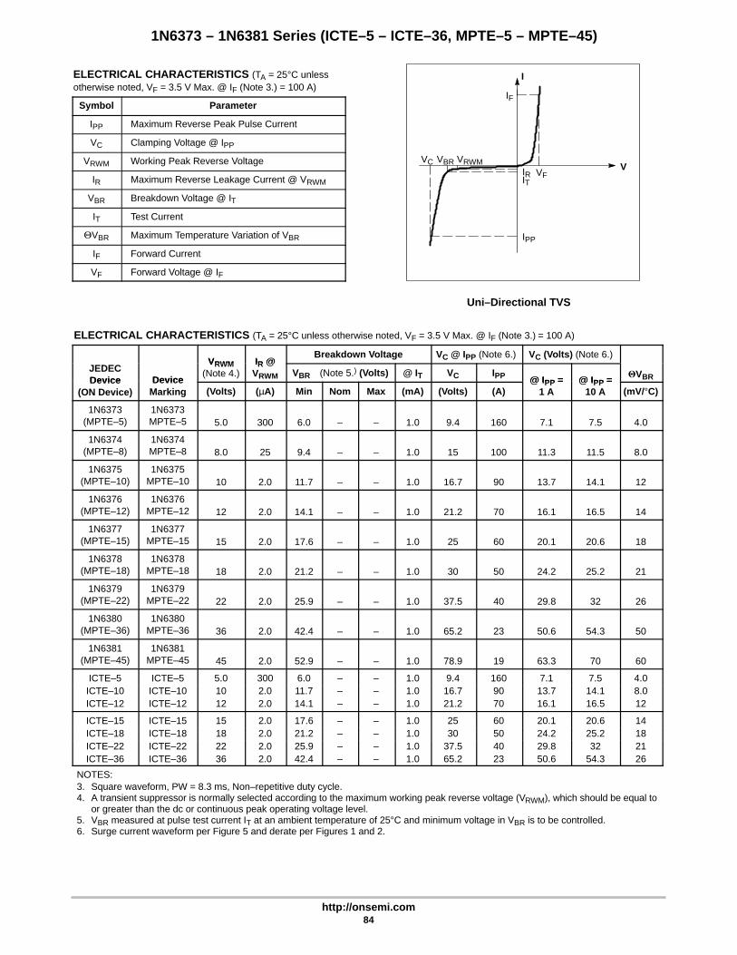
Uni–Directional TVS
IPP
IF
V
I
IRIT
VRWMVC VBRVF
1N6373 – 1N6381 Series (ICTE–5 – ICTE–36, MPTE–5 – MPTE–45)
http://onsemi.com84
ELECTRICAL CHARACTERISTICS (TA = 25°C unlessotherwise noted, VF = 3.5 V Max. @ IF (Note 3.) = 100 A)
Symbol Parameter
IPP Maximum Reverse Peak Pulse Current
VC Clamping Voltage @ IPP
VRWM Working Peak Reverse Voltage
IR Maximum Reverse Leakage Current @ VRWM
VBR Breakdown Voltage @ IT
IT Test Current
VBR Maximum Temperature Variation of VBR
IF Forward Current
VF Forward Voltage @ IF
ELECTRICAL CHARACTERISTICS (TA = 25°C unless otherwise noted, VF = 3.5 V Max. @ IF (Note 3.) = 100 A)
VRWM IR @Breakdown Voltage VC @ IPP (Note 6.) VC (Volts) (Note 6.)
JEDECDevice Device
VRWM(Note 4.)
IR @VRWM VBR (Note 5.) (Volts) @ IT VC IPP @ IPP = @ IPP =
VBRDevice(ON Device)
DeviceMarking (Volts) (µA) Min Nom Max (mA) (Volts) (A)
@ IPP =1 A
@ IPP =10 A (mV/°C)
1N6373(MPTE–5)
1N6373MPTE–5 5.0 300 6.0 – – 1.0 9.4 160 7.1 7.5 4.0
1N6374(MPTE–8)
1N6374MPTE–8 8.0 25 9.4 – – 1.0 15 100 11.3 11.5 8.0
1N6375(MPTE–10)
1N6375MPTE–10 10 2.0 11.7 – – 1.0 16.7 90 13.7 14.1 12
1N6376(MPTE–12)
1N6376MPTE–12 12 2.0 14.1 – – 1.0 21.2 70 16.1 16.5 14
1N6377(MPTE–15)
1N6377MPTE–15 15 2.0 17.6 – – 1.0 25 60 20.1 20.6 18
1N6378(MPTE–18)
1N6378MPTE–18 18 2.0 21.2 – – 1.0 30 50 24.2 25.2 21
1N6379(MPTE–22)
1N6379MPTE–22 22 2.0 25.9 – – 1.0 37.5 40 29.8 32 26
1N6380(MPTE–36)
1N6380MPTE–36 36 2.0 42.4 – – 1.0 65.2 23 50.6 54.3 50
1N6381(MPTE–45)
1N6381MPTE–45 45 2.0 52.9 – – 1.0 78.9 19 63.3 70 60
ICTE–5 ICTE–5 5.0 300 6.0 – – 1.0 9.4 160 7.1 7.5 4.0ICTE–10 ICTE–10 10 2.0 11.7 – – 1.0 16.7 90 13.7 14.1 8.0ICTE–12 ICTE–12 12 2.0 14.1 – – 1.0 21.2 70 16.1 16.5 12
ICTE–15 ICTE–15 15 2.0 17.6 – – 1.0 25 60 20.1 20.6 14ICTE–18 ICTE–18 18 2.0 21.2 – – 1.0 30 50 24.2 25.2 18ICTE–22 ICTE–22 22 2.0 25.9 – – 1.0 37.5 40 29.8 32 21ICTE–36 ICTE–36 36 2.0 42.4 – – 1.0 65.2 23 50.6 54.3 26
NOTES:3. Square waveform, PW = 8.3 ms, Non–repetitive duty cycle.4. A transient suppressor is normally selected according to the maximum working peak reverse voltage (VRWM), which should be equal to
or greater than the dc or continuous peak operating voltage level.5. VBR measured at pulse test current IT at an ambient temperature of 25°C and minimum voltage in VBR is to be controlled.6. Surge current waveform per Figure 5 and derate per Figures 1 and 2.

1N6373 – 1N6381 Series (ICTE–5 – ICTE–36, MPTE–5 – MPTE–45)
http://onsemi.com85
Figure 1. Pulse Rating Curve
100
80
60
40
20
00 25 50 75 100 125 150 175 200
PE
AK
PU
LSE
DE
RAT
ING
IN %
OF
PE
AK
PO
WE
R O
R C
UR
RE
NT
@ T
A=
25C°
TA, AMBIENT TEMPERATURE (°C)
Figure 2. Pulse Derating Curve
5
4
3
2
1
25 50 75 100 125 150 175 200
P D, S
TE
AD
Y S
TAT
E P
OW
ER
DIS
SIP
AT
ION
(W
AT
TS
)
TL, LEAD TEMPERATURE (°C)
3/8″
3/8″
00
100
50
00 1 2 3 4
t, TIME (ms)
, VA
LUE
(%
)
tr ≤ 10 s
tP
PEAK VALUE - IPP
HALF VALUE -IPP
2
PULSE WIDTH (tP) IS DEFINED ASTHAT POINT WHERE THE PEAKCURRENT DECAYS TO 50% OF IPP.
1µs 10µs 100µs 1 ms 10 ms
100
10
1
tP, PULSE WIDTH
PP
K, P
EA
K P
OW
ER
(kW
)NONREPETITIVEPULSE WAVEFORMSHOWN IN FIGURE 5
0.1µs
I PP
Figure 3. Capacitance versus Breakdown Voltage
Figure 4. Steady State Power Derating Figure 5. Pulse Waveform
1N6373, ICTE-5, MPTE-5,through
1N6389, ICTE-45, C, MPTE-45, C
VBR, BREAKDOWN VOLTAGE (VOLTS)
1 10 100 1000
10,000
1000
100
10
C, C
APA
CIT
AN
CE
(pF
)
MEASURED @ZERO BIAS
MEASURED @ VRWM

1N6373 – 1N6381 Series (ICTE–5 – ICTE–36, MPTE–5 – MPTE–45)
http://onsemi.com86
1N6373, ICTE-5, MPTE-5,through
1N6389, ICTE-45, C, MPTE-45, C
1.5KE6.8CAthrough
1.5KE200CA
Figure 6. Dynamic Impedance
1000
500
200
100
50
20
10
5
2
1
1000
500
200
100
50
20
10
5
2
10.3 0.5 0.7 1 2 3 5 7 10 20 30
∆VBR, INSTANTANEOUS INCREASE IN VBR ABOVE VBR(NOM) (VOLTS)
0.3 0.5 0.7 1 2 3 5 7 10 20 30
∆VBR, INSTANTANEOUS INCREASE IN VBR ABOVE VBR(NOM) (VOLTS)
I T, T
ES
T C
UR
RE
NT
(AM
PS
)
VBR(MIN)=6.0 to 11.7VTL=25°CtP=10µs
VBR(NOM)=6.8 to 13V
20V24V 43V
75V
180V
120V
19V21.2V 42.4V
Figure 7. Typical Derating Factor for Duty Cycle
DE
RAT
ING
FA
CT
OR
1 ms
10 µs
1
0.7
0.5
0.3
0.05
0.1
0.2
0.01
0.02
0.03
0.07
100 µs
0.1 0.2 0.5 2 5 10 501 20 100
D, DUTY CYCLE (%)
PULSE WIDTH10 ms
TL=25°CtP=10µs
I T, T
ES
T C
UR
RE
NT
(AM
PS
)

1N6373 – 1N6381 Series (ICTE–5 – ICTE–36, MPTE–5 – MPTE–45)
http://onsemi.com87
APPLICATION NOTES
RESPONSE TIME
In most applications, the transient suppressor device isplaced in parallel with the equipment or component to beprotected. In this situation, there is a time delay associatedwith the capacitance of the device and an overshootcondition associated with the inductance of the device andthe inductance of the connection method. The capacitanceeffect is of minor importance in the parallel protectionscheme because it only produces a time delay in thetransition from the operating voltage to the clamp voltage asshown in Figure 8.
The inductive effects in the device are due to actualturn-on time (time required for the device to go from zerocurrent to full current) and lead inductance. This inductiveeffect produces an overshoot in the voltage across theequipment or component being protected as shown inFigure 9. Minimizing this overshoot is very important in theapplication, since the main purpose for adding a transientsuppressor is to clamp voltage spikes. These devices haveexcellent response time, typically in the picosecond rangeand negligible inductance. However, external inductiveeffects could produce unacceptable overshoot. Proper
circuit layout, minimum lead lengths and placing thesuppressor device as close as possible to the equipment orcomponents to be protected will minimize this overshoot.
Some input impedance represented by Zin is essential toprevent overstress of the protection device. This impedanceshould be as high as possible, without restricting the circuitoperation.
DUTY CYCLE DERATINGThe data of Figure 1 applies for non-repetitive conditions
and at a lead temperature of 25°C. If the duty cycle increases,the peak power must be reduced as indicated by the curvesof Figure 7. Average power must be derated as the lead orambient temperature rises above 25°C. The average powerderating curve normally given on data sheets may benormalized and used for this purpose.
At first glance the derating curves of Figure 7 appear to bein error as the 10 ms pulse has a higher derating factor thanthe 10 µs pulse. However, when the derating factor for agiven pulse of Figure 7 is multiplied by the peak power valueof Figure 1 for the same pulse, the results follow theexpected trend.
TYPICAL PROTECTION CIRCUIT
Vin
VL
V
Vin
Vin (TRANSIENT)VL
td
V
VL
Vin (TRANSIENT)
Zin
LOAD
OVERSHOOT DUE TOINDUCTIVE EFFECTS
tD = TIME DELAY DUE TO CAPACITIVE EFFECTt t
Figure 8. Figure 9.

Semiconductor Components Industries, LLC, 2001
May, 2001 – Rev. 088 Publication Order Number:
1N6382/D
1N6382 - 1N6389 Series(ICTE-10C - ICTE-36C,MPTE-8C - MPTE-45C)
1500 Watt Peak PowerMosorb Zener TransientVoltage Suppressors
Bidirectional*Mosorb devices are designed to protect voltage sensitive
components from high voltage, high–energy transients. They haveexcellent clamping capability, high surge capability, low zenerimpedance and fast response t ime. These devices areON Semiconductor’s exclusive, cost-effective, highly reliableSurmetic axial leaded package and are ideally-suited for use incommunication systems, numerical controls, process controls,medical equipment, business machines, power supplies and manyother industrial/consumer applications, to protect CMOS, MOS andBipolar integrated circuits.
Specification Features:• Working Peak Reverse Voltage Range – 8 V to 45 V
• Peak Power – 1500 Watts @ 1 ms
• ESD Rating of Class 3 (>16 KV) per Human Body Model
• Maximum Clamp Voltage @ Peak Pulse Current
• Low Leakage < 5 µA Above 10 V
• Response Time is Typically < 1 ns
Mechanical Characteristics:CASE: Void-free, transfer-molded, thermosetting plasticFINISH: All external surfaces are corrosion resistant and leads arereadily solderableMAXIMUM LEAD TEMPERATURE FOR SOLDERING PURPOSES:230°C, 1/16″ from the case for 10 secondsPOLARITY: Cathode band does not imply polarityMOUNTING POSITION: Any
MAXIMUM RATINGS
Rating Symbol Value Unit
Peak Power Dissipation (Note 1.)@ TL ≤ 25°C
PPK 1500 Watts
Steady State Power Dissipation@ TL ≤ 75°C, Lead Length = 3/8″Derated above TL = 75°C
PD 5.0
20
Watts
mW/°C
Thermal Resistance, Junction–to–Lead RJL 20 °C/W
Operating and StorageTemperature Range
TJ, Tstg – 65 to+175
°C
1. Nonrepetitive current pulse per Figure 4 and derated above TA = 25°Cper Figure 2.
*Please see 1N6373 – 1N6381 (ICTE–5 – ICTE–36, MPTE–5 – MPTE–45)for Unidirectional Devices
AXIAL LEADCASE 41APLASTIC
http://onsemi.com
L = Assembly LocationMPTE–xxC = ON Device CodeICTE–xxC = ON Device Code1N63xx = JEDEC Device CodeYY = YearWW = Work Week
Device Package Shipping
ORDERING INFORMATION
MPTE–xxC Axial Lead 500 Units/Box
MPTE–xxCRL4 Axial Lead 1500/Tape & Reel
ICTE–xxC Axial Lead 500 Units/Box
ICTE–xxCRL4 Axial Lead 1500/Tape & Reel
LICTE–xxCYYWW
1N63xx Axial Lead 500 Units/Box
1N63xxRL4 Axial Lead 1500/Tape & Reel
LMPTE–xxC1N63xxYYWW

Bi–Directional TVS
IPP
IPP
V
I
IRIT
ITIRVRWMVC VBR
VRWM VCVBR
1N6382 – 1N6389 Series (ICTE–10C – ICTE–36C, MPTE–8C – MPTE–45C)
http://onsemi.com89
ELECTRICAL CHARACTERISTICS(TA = 25°C unless otherwise noted)
Symbol Parameter
IPP Maximum Reverse Peak Pulse Current
VC Clamping Voltage @ IPP
VRWM Working Peak Reverse Voltage
IR Maximum Reverse Leakage Current @ VRWM
VBR Breakdown Voltage @ IT
IT Test Current
VBR Maximum Temperature Variation of VBR
ELECTRICAL CHARACTERISTICS (TA = 25°C unless otherwise noted)
VRWM IR @Breakdown Voltage VC @ IPP (Note 4.) VC (Volts) (Note 4.)
JEDECDevice Device
VRWM(Note 2.)
IR @VRWM VBR (Note 3.) (Volts) @ IT VC IPP @ IPP @ IPP
VBRDevice(ON Device)
DeviceMarking (Volts) (µA) Min Nom Max (mA) (Volts) (A)
@ IPP= 1 A
@ IPP= 10 A (mV/°C)
1N6382(MPTE–8C)
1N6382MPTE–8C 8.0 25 9.4 – – 1.0 15 100 11.3 11.5 8.0
1N6383(MPTE–10C)
1N6383MPTE–10C 10 2.0 11.7 – – 1.0 16.7 90 13.7 14.1 12
1N6384(MPTE–12C)
1N6384MPTE–12C 12 2.0 14.1 – – 1.0 21.2 70 16.1 16.5 14
1N6385(MPTE–15C)
1N6385MPTE–15C 15 2.0 17.6 – – 1.0 25 60 20.1 20.6 18
1N6386(MPTE–18C)
1N6386MPTE–18C 18 2.0 21.2 – – 1.0 30 50 24.2 25.2 21
1N6387(MPTE–22C)
1N6387MPTE–22C 22 2.0 25.9 – – 1.0 37.5 40 29.8 32 26
1N6388(MPTE–36C)
1N6388MPTE–36C 36 2.0 42.4 – – 1.0 65.2 23 50.6 54.3 50
1N6389(MPTE–45C)
1N6389MPTE–45C 45 2.0 52.9 – – 1.0 78.9 19 63.3 70 60
ICTE–10C ICTE–10C 10 2.0 11.7 – – 1.0 16.7 90 13.7 14.1 8.0ICTE–12C ICTE–12C 12 2.0 14.1 – – 1.0 21.2 70 16.1 16.5 12
ICTE–15C ICTE–15C 15 2.0 17.6 – – 1.0 25 60 20.1 20.6 14ICTE–18C ICTE–18C 18 2.0 21.2 – – 1.0 30 50 24.2 25.2 18ICTE–22C ICTE–22C 22 2.0 25.9 – – 1.0 37.5 40 29.8 32 21ICTE–36C ICTE–36C 36 2.0 42.4 – – 1.0 65.2 23 50.6 54.3 26
NOTES:2. A transient suppressor is normally selected according to the maximum working peak reverse voltage (VRWM), which should be equal to
or greater than the dc or continuous peak operating voltage level.3. VBR measured at pulse test current IT at an ambient temperature of 25°C and minimum voltage in VBR is to be controlled.4. Surge current waveform per Figure 4 and derate per Figures 1 and 2.

1N6382 – 1N6389 Series (ICTE–10C – ICTE–36C, MPTE–8C – MPTE–45C)
http://onsemi.com90
Figure 1. Pulse Rating Curve
100
80
60
40
20
00 25 50 75 100 125 150 175 200
PE
AK
PU
LSE
DE
RAT
ING
IN %
OF
PE
AK
PO
WE
R O
R C
UR
RE
NT
@ T
A=
25C°
TA, AMBIENT TEMPERATURE (°C)
Figure 2. Pulse Derating Curve
5
4
3
2
1
25 50 75 100 125 150 175 200
P D, S
TE
AD
Y S
TAT
E P
OW
ER
DIS
SIP
AT
ION
(W
AT
TS
)
TL, LEAD TEMPERATURE (°C)
3/8″
3/8″
00
100
50
00 1 2 3 4
t, TIME (ms)
, VA
LUE
(%
)
tr ≤ 10 s
tP
PEAK VALUE - IPP
HALF VALUE -IPP
2
PULSE WIDTH (tP) IS DEFINED ASTHAT POINT WHERE THE PEAKCURRENT DECAYS TO 50% OF IPP.
1µs 10µs 100µs 1 ms 10 ms
100
10
1
tP, PULSE WIDTH
PP
K, P
EA
K P
OW
ER
(kW
)NONREPETITIVEPULSE WAVEFORMSHOWN IN FIGURE 5
0.1µs
I PP
Figure 3. Steady State Power Derating Figure 4. Pulse Waveform

1N6382 – 1N6389 Series (ICTE–10C – ICTE–36C, MPTE–8C – MPTE–45C)
http://onsemi.com91
1N6373, ICTE-5, MPTE-5,through
1N6389, ICTE-45, C, MPTE-45, C
1.5KE6.8CAthrough
1.5KE200CA
Figure 5. Dynamic Impedance
1000
500
200
100
50
20
10
5
2
1
1000
500
200
100
50
20
10
5
2
10.3 0.5 0.7 1 2 3 5 7 10 20 30
∆VBR, INSTANTANEOUS INCREASE IN VBR ABOVE VBR(NOM) (VOLTS)
0.3 0.5 0.7 1 2 3 5 7 10 20 30
∆VBR, INSTANTANEOUS INCREASE IN VBR ABOVE VBR(NOM) (VOLTS)
I T, T
ES
T C
UR
RE
NT
(AM
PS
)
VBR(MIN)=6.0 to 11.7VTL=25°CtP=10µs
VBR(NOM)=6.8 to 13V
20V24V 43V
75V
180V
120V
19V21.2V 42.4V
Figure 6. Typical Derating Factor for Duty Cycle
DE
RAT
ING
FA
CT
OR
1 ms
10 µs
1
0.7
0.5
0.3
0.05
0.1
0.2
0.01
0.02
0.03
0.07
100 µs
0.1 0.2 0.5 2 5 10 501 20 100
D, DUTY CYCLE (%)
PULSE WIDTH10 ms
TL=25°CtP=10µs
I T, T
ES
T C
UR
RE
NT
(AM
PS
)

1N6382 – 1N6389 Series (ICTE–10C – ICTE–36C, MPTE–8C – MPTE–45C)
http://onsemi.com92
APPLICATION NOTES
RESPONSE TIME
In most applications, the transient suppressor device isplaced in parallel with the equipment or component to beprotected. In this situation, there is a time delay associatedwith the capacitance of the device and an overshootcondition associated with the inductance of the device andthe inductance of the connection method. The capacitanceeffect is of minor importance in the parallel protectionscheme because it only produces a time delay in thetransition from the operating voltage to the clamp voltage asshown in Figure 7.
The inductive effects in the device are due to actualturn-on time (time required for the device to go from zerocurrent to full current) and lead inductance. This inductiveeffect produces an overshoot in the voltage across theequipment or component being protected as shown inFigure 8. Minimizing this overshoot is very important in theapplication, since the main purpose for adding a transientsuppressor is to clamp voltage spikes. These devices haveexcellent response time, typically in the picosecond rangeand negligible inductance. However, external inductiveeffects could produce unacceptable overshoot. Proper
circuit layout, minimum lead lengths and placing thesuppressor device as close as possible to the equipment orcomponents to be protected will minimize this overshoot.
Some input impedance represented by Zin is essential toprevent overstress of the protection device. This impedanceshould be as high as possible, without restricting the circuitoperation.
DUTY CYCLE DERATINGThe data of Figure 1 applies for non-repetitive conditions
and at a lead temperature of 25°C. If the duty cycle increases,the peak power must be reduced as indicated by the curvesof Figure 6. Average power must be derated as the lead orambient temperature rises above 25°C. The average powerderating curve normally given on data sheets may benormalized and used for this purpose.
At first glance the derating curves of Figure 6 appear to bein error as the 10 ms pulse has a higher derating factor thanthe 10 µs pulse. However, when the derating factor for agiven pulse of Figure 6 is multiplied by the peak power valueof Figure 1 for the same pulse, the results follow theexpected trend.
TYPICAL PROTECTION CIRCUIT
Vin
VL
V
Vin
Vin (TRANSIENT)VL
td
V
VL
Vin (TRANSIENT)
Zin
LOAD
OVERSHOOT DUE TOINDUCTIVE EFFECTS
tD = TIME DELAY DUE TO CAPACITIVE EFFECTt t
Figure 7. Figure 8.
http://onsemi.com93
CHAPTER 4Transient Voltage Suppressors –
Surface Mounted Data Sheets
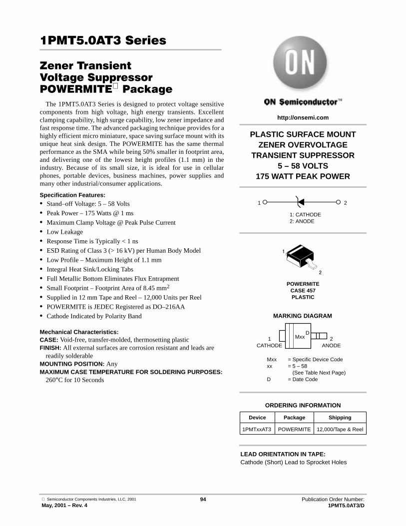
Semiconductor Components Industries, LLC, 2001
May, 2001 – Rev. 494 Publication Order Number:
1PMT5.0AT3/D
1PMT5.0AT3 Series
Zener TransientVoltage SuppressorPOWERMITE Package
The 1PMT5.0AT3 Series is designed to protect voltage sensitivecomponents from high voltage, high energy transients. Excellentclamping capability, high surge capability, low zener impedance andfast response time. The advanced packaging technique provides for ahighly efficient micro miniature, space saving surface mount with itsunique heat sink design. The POWERMITE has the same thermalperformance as the SMA while being 50% smaller in footprint area,and delivering one of the lowest height profiles (1.1 mm) in theindustry. Because of its small size, it is ideal for use in cellularphones, portable devices, business machines, power supplies andmany other industrial/consumer applications.
Specification Features:• Stand–off Voltage: 5 – 58 Volts
• Peak Power – 175 Watts @ 1 ms
• Maximum Clamp Voltage @ Peak Pulse Current
• Low Leakage
• Response Time is Typically < 1 ns
• ESD Rating of Class 3 (> 16 kV) per Human Body Model
• Low Profile – Maximum Height of 1.1 mm
• Integral Heat Sink/Locking Tabs
• Full Metallic Bottom Eliminates Flux Entrapment
• Small Footprint – Footprint Area of 8.45 mm2
• Supplied in 12 mm Tape and Reel – 12,000 Units per Reel
• POWERMITE is JEDEC Registered as DO–216AA
• Cathode Indicated by Polarity Band
Mechanical Characteristics:CASE: Void-free, transfer-molded, thermosetting plasticFINISH: All external surfaces are corrosion resistant and leads are
readily solderableMOUNTING POSITION: AnyMAXIMUM CASE TEMPERATURE FOR SOLDERING PURPOSES:
260°C for 10 Seconds
PLASTIC SURFACE MOUNTZENER OVERVOLTAGE
TRANSIENT SUPPRESSOR5 – 58 VOLTS
175 WATT PEAK POWER
Device Package Shipping
ORDERING INFORMATION
1PMTxxAT3 POWERMITE 12,000/Tape & Reel
POWERMITECASE 457PLASTIC
http://onsemi.com
1 2
1: CATHODE2: ANODE
1
2
LEAD ORIENTATION IN TAPE:Cathode (Short) Lead to Sprocket Holes
Mxx = Specific Device Codexx = 5 – 58
= (See Table Next Page)D = Date Code
MARKING DIAGRAM
MxxD
1CATHODE
2ANODE
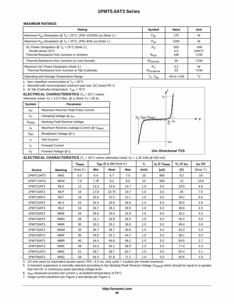
Uni–Directional TVS
IPP
IF
V
I
IRIT
VRWMVC VBRVF
1PMT5.0AT3 Series
http://onsemi.com95
MAXIMUM RATINGS
Rating Symbol Value Unit
Maximum Ppk Dissipation @ TA = 25°C, (PW–10/1000 s) (Note 1.) Ppk 175 W
Maximum Ppk Dissipation @ TA = 25°C, (PW–8/20 s) (Note 1.) Ppk 1000 W
DC Power Dissipation @ TA = 25°C (Note 2.)Derate above 25°C
Thermal Resistance from Junction to Ambient
°PD°
RθJA
5004.0248
°mWmW/°C°C/W
Thermal Resistance from Junction to Lead (Anode) RθJanode 35 °C/W
Maximum DC Power Dissipation (Note 3.)Thermal Resistance from Junction to Tab (Cathode)
°PD°RθJcathode
3.223
W°C/W
Operating and Storage Temperature Range TJ, Tstg –55 to +150 °C
1. Non–repetitive current pulse at TA = 25°C.2. Mounted with recommended minimum pad size, DC board FR–4.3. At Tab (Cathode) temperature, Ttab = 75°CELECTRICAL CHARACTERISTICS (TA = 25°C unlessotherwise noted, VF = 3.5 V Max. @ IF (Note 4.) = 35 A)
Symbol Parameter
IPP Maximum Reverse Peak Pulse Current
VC Clamping Voltage @ IPP
VRWM Working Peak Reverse Voltage
IR Maximum Reverse Leakage Current @ VRWM
VBR Breakdown Voltage @ IT
IT Test Current
IF Forward Current
VF Forward Voltage @ IF
ELECTRICAL CHARACTERISTICS (TL = 30°C unless otherwise noted, VF = 1.25 Volts @ 200 mA)
VRWM VBR @ IT (V) (Note 6.) IT IR @ VRWM VC @ IPP IPP (A)
Device Marking (Note 5.) Min Nom Max (mA) (A) (V) (Note 7.)
1PMT5.0AT3 MKE 5.0 6.4 6.7 7.0 10 800 9.2 19
1PMT7.0AT3 MKM 7.0 7.78 8.2 8.6 10 500 12 14.6
1PMT12AT3 MLE 12 13.3 14.0 14.7 1.0 5.0 19.9 8.8
1PMT16AT3 MLP 16 17.8 18.75 19.7 1.0 5.0 26 7.0
1PMT18AT3 MLT 18 20.0 21.0 22.1 1.0 5.0 29.2 6.0
1PMT22AT3 MLX 22 24.4 25.6 26.9 1.0 5.0 35.5 4.9
1PMT24AT3 MLZ 24 26.7 28.1 29.5 1.0 5.0 38.9 4.5
1PMT26AT3 MME 26 28.9 30.4 31.9 1.0 5.0 42.1 4.2
1PMT28AT3 MMG 28 31.1 32.8 34.4 1.0 5.0 45.4 3.9
1PMT30AT3 MMK 30 33.3 35.1 36.8 1.0 5.0 48.4 3.6
1PMT33AT3 MMM 33 36.7 38.7 40.6 1.0 5.0 53.3 3.3
1PMT36AT3 MMP 36 40.0 42.1 44.2 1.0 5.0 58.1 3.0
1PMT40AT3 MMR 40 44.4 46.8 49.1 1.0 5.0 64.5 2.7
1PMT48AT3 MMX 48 53.3 56.1 58.9 1.0 5.0 77.4 2.3
1PMT51AT3 MMZ 51 56.7 59.7 62.7 1.0 5.0 82.4 2.1
1PMT58AT3 MNG 58 64.4 67.8 71.2 1.0 5.0 93.6 1.9
4. 1/2 sine wave (or equivalent square wave), PW = 8.3 ms, duty cycle = 4 pulses per minute maximum.5. A transient suppressor is normally selected according to the Working Peak Reverse Voltage (VRWM) which should be equal to or greater
than the DC or continuous peak operating voltage level.6. VBR measured at pulse test current IT at ambient temperature of 25°C.7. Surge current waveform per Figure 2 and derate per Figure 4.
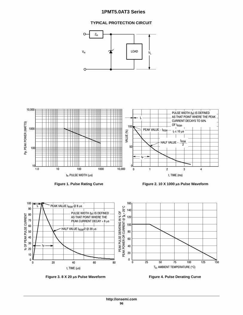
1PMT5.0AT3 Series
http://onsemi.com96
P ,
PE
AK
PO
WE
R (
WA
TT
S)
P
tP, PULSE WIDTH (s)
100
1000
10,000
1.0 10 10010
0 1 2 3 40
50
100
t, TIME (ms)
VA
LUE
(%
)
HALF VALUE -IRSM
2
PEAK VALUE - IRSM
tr
tr≤ 10 µs
TYPICAL PROTECTION CIRCUIT
Vin VL
Zin
LOAD
PE
AK
PU
LSE
DE
RAT
ING
IN %
OF
PE
AK
PO
WE
R O
R C
UR
RE
NT
@ T
A=
25C°
100
80
60
40
20
00 25 50 75 100 125 150
TA, AMBIENT TEMPERATURE (°C)
120
140
160
tP
PULSE WIDTH (tP) IS DEFINED
AS THAT POINT WHERE THE PEAK
CURRENT DECAYS TO 50%
OF IRSM.
Figure 1. Pulse Rating Curve Figure 2. 10 X 1000 s Pulse Waveform
100
90
80
70
60
50
40
30
20
10
00 20 40 60 80
t, TIME (s)
% O
F P
EA
K P
ULS
E C
UR
RE
NT
tP
tr
PULSE WIDTH (tP) IS DEFINED
AS THAT POINT WHERE THE
PEAK CURRENT DECAY = 8 s
PEAK VALUE IRSM @ 8 s
HALF VALUE IRSM/2 @ 20 s
Figure 3. 8 X 20 s Pulse Waveform
1000 10,000
Figure 4. Pulse Derating Curve

1PMT5.0AT3 Series
http://onsemi.com97
Figure 5. Typical Derating Factor for Duty Cycle
DE
RA
TIN
G F
AC
TO
R
1 ms
10 µs
10.7
0.5
0.3
0.05
0.1
0.2
0.01
0.02
0.03
0.07
100 µs
0.1 0.2 0.5 2 5 10 501 20 100
D, DUTY CYCLE (%)
PULSE WIDTH10 ms
Figure 6. Steady State Power Derating
1.2
1.0
0.8
0.6
0.4
0.2
0–55 25 85 150
T, TEMPERATURE (°C)
V, T
YP
ICA
L F
OR
WA
RD
VO
LTA
GE
(V
OLT
S)
F
Figure 7. Forward Voltage
25 50 75 100 125 175
3.5
2.5
2
1.5
1
0
T, TEMPERATURE (°C)
P
, MA
XIM
UM
PO
WE
R D
ISS
IPA
TIO
N (
W)
D
0.5
TL
150
3
10,000
1000
100
101 10 100
WORKING PEAK REVERSE VOLTAGE (VOLTS)
C, C
AP
AC
ITA
NC
E (
pF)
Figure 8. Capacitance versus Working PeakReverse Voltage
MEASURED @ 50% VRWM
MEASURED @ ZERO BIAS

Semiconductor Components Industries, LLC, 2001
May, 2001 – Rev. 498 Publication Order Number:
1SMA5.0AT3/D
1SMA5.0AT3 Series
400 Watt Peak Power ZenerTransient Voltage Suppressors
Unidirectional*The SMA series is designed to protect voltage sensitive
components from high voltage, high energy transients. They haveexcellent clamping capability, high surge capability, low zenerimpedance and fast response time. The SMA series is supplied inON Semiconductor’s exclusive, cost-effective, highly reliableSurmetic package and is ideally suited for use in communicationsystems, automotive, numerical controls, process controls, medicalequipment, business machines, power supplies and many otherindustrial/consumer applications.
Specification Features:• Working Peak Reverse Voltage Range – 5.0 V to 78 V
• Standard Zener Breakdown Voltage Range – 6.7 V to 91.25 V
• Peak Power – 400 Watts @ 1 ms
• ESD Rating of Class 3 (> 16 KV) per Human Body Model
• Response Time is Typically < 1 ns
• Flat Handling Surface for Accurate Placement
• Package Design for Top Slide or Bottom Circuit Board Mounting
• Low Profile Package
Mechanical Characteristics:CASE: Void-free, transfer-molded plasticFINISH: All external surfaces are corrosion resistant and leads are
readily solderableMAXIMUM CASE TEMPERATURE FOR SOLDERING PURPOSES:
260°C for 10 SecondsPOLARITY: Cathode indicated by molded polarity notch or polarity
bandMOUNTING POSITION: Any
MAXIMUM RATINGS
Please See the Table on the Following Page
PLASTIC SURFACE MOUNTZENER OVERVOLTAGE
TRANSIENT SUPPRESSORS5.0–78 VOLTS
400 WATTS PEAK POWER
Device Package Shipping
ORDERING INFORMATION
1SMAxxAT3 SMA 5000/Tape & Reel
SMACASE 403B
PLASTIC
http://onsemi.com
xx = Specific Device Code= (See Table on Page 100)
LL = Assembly LocationY = YearWW = Work Week
xxLLYWW
MARKING DIAGRAM
*Please see 1SMA10CAT3 to 1SMA78CAT3 forBidirectional devices.
†The “T3” suffix refers to a 13 inch reel.
CATHODE ANODE

Uni–Directional TVS
IPP
IF
V
I
IRIT
VRWMVC VBRVF
1SMA5.0AT3 Series
http://onsemi.com99
MAXIMUM RATINGS
Rating Symbol Value Unit
Peak Power Dissipation (Note 1.) @ TL = 25°C, Pulse Width = 1 ms PPK 400 W
DC Power Dissipation @ TL = 75°CMeasured Zero Lead Length (Note 2.)Derate Above 75°C
Thermal Resistance from Junction to Lead
PD
RJL
1.5
2050
W
mW/°C°C/W
DC Power Dissipation (Note 3.) @ TA = 25°CDerate Above 25°C
Thermal Resistance from Junction to Ambient
PD
RJA
0.54.0250
WmW/°C°C/W
Forward Surge Current (Note 4.) @ TA = 25°C IFSM 40 A
Operating and Storage Temperature Range TJ, Tstg –65 to +150 °C
1. 10 X 1000 s, non–repetitive2. 1″ square copper pad, FR–4 board3. FR–4 board, using ON Semiconductor minimum recommended footprint, as shown in 403B case outline dimensions spec.4. 1/2 sine wave (or equivalent square wave), PW = 8.3 ms, duty cycle = 4 pulses per minute maximum.
ELECTRICAL CHARACTERISTICS(TA = 25°C unless otherwise noted, VF = 3.5 V Max. @IF = 30 A for all types) (Note 5.)
Symbol Parameter
IPP Maximum Reverse Peak Pulse Current
VC Clamping Voltage @ IPP
VRWM Working Peak Reverse Voltage
IR Maximum Reverse Leakage Current @ VRWM
VBR Breakdown Voltage @ IT
IT Test Current
IF Forward Current
VF Forward Voltage @ IF
5. 1/2 sine wave or equivalent, PW = 8.3 ms, non–repetitiveduty cycle.

1SMA5.0AT3 Series
http://onsemi.com100
ELECTRICAL CHARACTERISTICS
VRWMBreakdown Voltage VC @ IPP (Note 8.)
Device
VRWM(Note 6.) IR @ VRWM VBR (Volts) (Note 7.) @ IT VC IPP
DeviceDevice
Marking Volts µA Min Nom Max mA Volts Amps
1SMA5.0AT3 QE 5.0 400 6.4 6.7 7.0 10 9.2 43.51SMA6.0AT3 QG 6.0 400 6.67 7.02 7.37 10 10.3 38.81SMA6.5AT3 QK 6.5 250 7.22 7.6 7.98 10 11.2 35.71SMA7.0AT3 QM 7.0 250 7.78 8.19 8.6 10 12.0 33.3
1SMA7.5AT3 QP 7.5 50 8.33 8.77 9.21 1 12.9 31.01SMA8.0AT3 QR 8.0 25 8.89 9.36 9.83 1 13.6 29.41SMA8.5AT3 QT 8.5 5.0 9.44 9.92 10.4 1 14.4 27.81SMA9.0AT3 QV 9.0 2.5 10 10.55 11.1 1 15.4 26.0
1SMA10AT3 QX 10 2.5 11.1 11.7 12.3 1 17.0 23.51SMA11AT3 QZ 11 2.5 12.2 12.85 13.5 1 18.2 22.01SMA12AT3 RE 12 2.5 13.3 14.0 14.7 1 19.9 20.11SMA13AT3 RG 13 2.5 14.4 15.15 15.9 1 21.5 18.6
1SMA14AT3 RK 14 2.5 15.6 16.4 17.2 1 23.2 17.21SMA15AT3 RM 15 2.5 16.7 17.6 18.5 1 24.4 16.41SMA16AT3 RP 16 2.5 17.8 18.75 19.7 1 26.0 15.41SMA17AT3 RR 17 2.5 18.9 19.9 20.9 1 27.6 14.5
1SMA18AT3 RT 18 2.5 20 21.05 22.1 1 29.2 13.71SMA20AT3 RV 20 2.5 22.2 23.35 24.5 1 32.4 12.31SMA22AT3 RX 22 2.5 24.4 25.65 26.9 1 35.5 11.31SMA24AT3 RZ 24 2.5 26.7 28.1 29.5 1 38.9 10.3
1SMA26AT3 SE 26 2.5 28.9 30.4 31.9 1 42.1 9.51SMA28AT3 SG 28 2.5 31.1 32.75 34.4 1 45.4 8.81SMA30AT3 SK 30 2.5 33.3 35.05 36.8 1 48.4 8.31SMA33AT3 SM 33 2.5 36.7 38.65 40.6 1 53.3 7.5
1SMA36AT3 SP 36 2.5 40 42.1 44.2 1 58.1 6.91SMA40AT3 SR 40 2.5 44.4 46.75 49.1 1 64.5 6.21SMA43AT3 ST 43 2.5 47.8 50.3 52.8 1 69.4 5.81SMA45AT3 SV 45 2.5 50 52.65 55.3 1 72.2 5.5
1SMA48AT3 SX 48 2.5 53.3 56.1 58.9 1 77.4 5.21SMA51AT3 SZ 51 2.5 56.7 59.7 62.7 1 82.4 4.91SMA54AT3 TE 54 2.5 60 63.15 66.3 1 87.1 4.61SMA58AT3 TG 58 2.5 64.4 67.8 71.5 1 93.6 4.3
1SMA60AT3 TK 60 2.5 66.7 70.2 73.7 1 96.8 4.11SMA64AT3 TM 64 2.5 71.1 74.85 78.6 1 103 3.91SMA70AT3 TP 70 2.5 77.8 81.9 86.0 1 113 3.51SMA75AT3 TR 75 2.5 83.3 87.7 92.1 1 121 3.31SMA78AT3 TS 78 2.5 86.7 91.25 95.8 1 126 3.2
6. A transient suppressor is normally selected according to the working peak reverse voltage (VRWM), which should be equal to or greater thanthe DC or continuous peak operating voltage level
7. VBR measured at pulse test current IT at an ambient temperature of 25°C8. Surge current waveform per Figure 2 and derate per Figure 3

1SMA5.0AT3 Series
http://onsemi.com101
RATING AND TYPICAL CHARACTERISTIC CURVES
TA = 25°C
PW (ID) IS DEFINED AS THE
POINT WHERE THE PEAK CURRENT
DECAYS TO 50% OF Ipp.
≤ 10 µs
PEAK VALUE
Ippm
HALF VALUE - Ipp/2
10/1000 µs WAVEFORM
AS DEFINED BY R.E.A.
td
120
100
80
60
40
00 1 2 3 4
I ppm
, PE
AK
PU
LSE
CU
RR
EN
T (%
)
20
510-4
100
0.1 1 10
10
1
0.1
tP, PULSE WIDTH (ms)
P pk
NONREPETITIVE
PULSE WAVEFORM
SHOWN IN FIGURE 2.
TA = 25°C
, PE
AK
PO
WE
R (
kW)
0.010.001
t, TIME (ms)
120
100
80
60
40
00 40 80 120 160
TA, AMBIENT TEMPERATURE (°C)
PE
AK
PU
LSE
DE
RAT
ING
IN %
OF
20
200
PE
AK
PO
WE
R O
R C
UR
RE
NT
10 x 1000 WAVEFORM
AS DEFINED BY R.E.A.
10,000
1,000
100
101 2 5 10 20 50 100 200
V(BR), BREAKDOWN VOLTAGE (VOLTS)
MEASURED AT
ZERO BIAS
MEASURED AT
STAND-OFF
VOLTAGE, VWM
TJ = 25°C
f = 1 MHz
Vsig = 50 mVp-p
0
6
T, TEMPERATURE (°C)
50 100 150
PD
, MA
XIM
UM
PO
WE
R D
ISS
IPA
TIO
N (
WA
TT
S)
5
4
3
2
0
1
Figure 1. Pulse Rating Curve Figure 2. Pulse Waveform
Figure 3. Pulse Derating Curve Figure 4. Typical Junction Capacitance
Figure 5. Steady State Power Derating
C, C
APA
CIT
AN
CE
(pF
)
@ TL = 75°CPD = 1.5 W
@ TA = 25°CPD = 0.5 W
25 75 125

Semiconductor Components Industries, LLC, 2001
May, 2001 – Rev. 4102 Publication Order Number:
1SMA10CAT3/D
1SMA10CAT3 Series
400 Watt Peak Power ZenerTransient Voltage Suppressors
Bidirectional*The SMA series is designed to protect voltage sensitive
components from high voltage, high energy transients. They haveexcellent clamping capability, high surge capability, low zenerimpedance and fast response time. The SMA series is supplied inON Semiconductor’s exclusive, cost-effective, highly reliableSurmetic package and is ideally suited for use in communicationsystems, automotive, numerical controls, process controls, medicalequipment, business machines, power supplies and many otherindustrial/consumer applications.
Specification Features:• Working Peak Reverse Voltage Range – 10 V to 78 V
• Standard Zener Breakdown Voltage Range – 11.7 V to 91.3 V
• Peak Power – 400 Watts @ 1 ms
• ESD Rating of Class 3 (> 16 KV) per Human Body Model
• Response Time is Typically < 1 ns
• Flat Handling Surface for Accurate Placement
• Package Design for Top Slide or Bottom Circuit Board Mounting
• Low Profile Package
Mechanical Characteristics:CASE: Void-free, transfer-molded plasticFINISH: All external surfaces are corrosion resistant and leads are
readily solderableMAXIMUM CASE TEMPERATURE FOR SOLDERING PURPOSES:
260°C for 10 SecondsPOLARITY: Cathode polarity notch does not indicate polarityMOUNTING POSITION: Any
MAXIMUM RATINGS
Rating Symbol Value Unit
Peak Power Dissipation (Note 1.)@ TL = 25°C, Pulse Width = 1 ms
PPK 400 W
DC Power Dissipation @ TL = 75°CMeasured Zero Lead Length (Note 2.)Derate Above 75°C
Thermal Resistance from Junction to Lead
PD
RJL
1.5
2050
W
mW/°C°C/W
DC Power Dissipation (Note 3.) @ TA = 25°CDerate Above 25°C
Thermal Resistance from Junctionto Ambient
PD
RJA
0.5
4.0250
W
mW/°C°C/W
Operating and StorageTemperature Range
TJ, Tstg –65 to+150
°C
1. 10 X 1000 s, non–repetitive2. 1″ square copper pad, FR–4 board3. FR–4 board, using ON Semiconductor minimum recommended footprint, as
shown in 403B case outline dimensions spec.
*Please see 1SMA5.0AT3 to 1SMA78AT3 for Unidirectional devices.
PLASTIC SURFACE MOUNTZENER OVERVOLTAGE
TRANSIENT SUPPRESSORS10–78 VOLTS VR
400 WATTS PEAK POWER
Device Package Shipping
ORDERING INFORMATION
1SMAxxCAT3 SMA 5000/Tape & Reel
SMACASE 403B
PLASTIC
http://onsemi.com
xxC = Specific Device Code= (See Table Next Page)
LL = Assembly LocationY = YearWW = Work Week
xxCLLYWW
MARKING DIAGRAM
†The “T3” suffix refers to a 13 inch reel.

Bi–Directional TVS
IPP
IPP
V
I
IRIT
ITIRVRWMVC VBR
VRWM VCVBR
1SMA10CAT3 Series
http://onsemi.com103
ELECTRICAL CHARACTERISTICS(TA = 25°C unless otherwise noted)
Symbol Parameter
IPP Maximum Reverse Peak Pulse Current
VC Clamping Voltage @ IPP
VRWM Working Peak Reverse Voltage
IR Maximum Reverse Leakage Current @ VRWM
VBR Breakdown Voltage @ IT
IT Test Current
ELECTRICAL CHARACTERISTICS
VRWMBreakdown Voltage VC @ IPP (Note 6.)
Device
VRWM(Note 4.) IR @ VRWM VBR (Volts) (Note 5.) @ IT VC IPP
DeviceDevice
Marking Volts µA Min Nom Max mA Volts Amps
1SMA10CAT3 QXC 10 2.5 11.1 11.69 12.27 1.0 17.0 23.51SMA11CAT3 QZC 11 2.5 12.2 12.84 13.48 1.0 18.2 22.01SMA12CAT3 REC 12 2.5 13.3 14.00 14.70 1.0 19.9 20.11SMA13CAT3 RGC 13 2.5 14.4 15.16 15.92 1.0 21.5 18.6
1SMA14CAT3 RKC 14 2.5 15.6 16.42 17.24 1.0 23.2 17.21SMA15CAT3 RMC 15 2.5 16.7 17.58 18.46 1.0 24.4 16.41SMA16CAT3 RPC 16 2.5 17.8 18.74 19.67 1.0 26.0 15.41SMA17CAT3 RRC 17 2.5 18.9 19.90 20.89 1.0 27.6 14.5
1SMA18CAT3 RTC 18 2.5 20 21.06 22.11 1.0 29.2 13.71SMA20CAT3 RVC 20 2.5 22.2 23.37 24.54 1.0 32.4 12.31SMA22CAT3 RXC 22 2.5 24.4 25.69 26.97 1.0 35.5 11.31SMA24CAT3 RZC 24 2.5 26.7 28.11 29.51 1.0 38.9 10.3
1SMA26CAT3 SEC 26 2.5 28.9 30.42 31.94 1.0 42.1 9.51SMA28CAT3 SGC 28 2.5 31.1 32.74 34.37 1.0 45.4 8.81SMA30CAT3 SKC 30 2.5 33.3 35.06 36.81 1.0 48.4 8.31SMA33CAT3 SMC 33 2.5 36.7 38.63 40.56 1.0 53.3 7.5
1SMA36CAT3 SPC 36 2.5 40 42.11 44.21 1.0 58.1 6.91SMA40CAT3 SRC 40 2.5 44.4 46.74 49.07 1.0 64.5 6.21SMA43CAT3 STC 43 2.5 47.8 50.32 52.83 1.0 69.4 5.81SMA45CAT3 SVC 45 2.5 50 52.63 55.26 1.0 72.2 5.5
1SMA48CAT3 SXC 48 2.5 53.3 56.11 58.91 1.0 77.4 5.21SMA51CAT3 SZC 51 2.5 56.7 59.69 62.67 1.0 82.4 4.91SMA54CAT3 TEC 54 2.5 60 63.16 66.32 1.0 87.1 4.61SMA58CAT3 TGC 58 2.5 64.4 67.79 71.18 1.0 93.6 4.3
1SMA60CAT3 TKC 60 2.5 66.7 70.21 73.72 1.0 96.8 4.11SMA64CAT3 TMC 64 2.5 71.1 74.84 78.58 1.0 103 3.91SMA70CAT3 TPC 70 2.5 77.8 81.90 85.99 1.0 113 3.51SMA75CAT3 TRC 75 2.5 83.3 87.69 92.07 1.0 121 3.31SMA78CAT3 TTC 78 2.5 86.7 91.27 95.83 1.0 126 3.2
4. A transient suppressor is normally selected according to the working peak reverse voltage (VRWM), which should be equal to or greater thanthe DC or continuous peak operating voltage level
5. VBR measured at pulse test current IT at an ambient temperature of 25°C6. Surge current waveform per Figure 2 and derate per Figure 3

1SMA10CAT3 Series
http://onsemi.com104
RATING AND TYPICAL CHARACTERISTIC CURVES
TA = 25°C
PW (ID) IS DEFINED AS THE
POINT WHERE THE PEAK CURRENT
DECAYS TO 50% OF Ipp.
= 10 µs
PEAK VALUE
Ippm
HALF VALUE - Ipp/2
10/1000 µs WAVEFORM
AS DEFINED BY R.E.A.
td
120
100
80
60
40
00 1 2 3 4
20
5
Figure 1. Pulse Rating Curve
10-4
100
0.1 1 10
10
1
0.1
tP, PULSE WIDTH (ms)
P pk
NONREPETITIVE
PULSE WAVEFORM
SHOWN IN FIGURE 2.
TA = 25°C
, PE
AK
PO
WE
R (
kW)
0.010.001
Figure 2. Pulse Waveform
t, TIME (ms)
I ppm
, PE
AK
PU
LSE
CU
RR
EN
T (%
)
Figure 3. Pulse Derating Curve
120
100
80
60
40
00 40 80 120 160
TA, AMBIENT TEMPERATURE (°C)
PE
AK
PU
LSE
DE
RAT
ING
IN %
OF
20
200
PE
AK
PO
WE
R O
R C
UR
RE
NT
10 x 1000 WAVEFORM
AS DEFINED BY R.E.A.

Semiconductor Components Industries, LLC, 2001
May, 2001 – Rev. 4105 Publication Order Number:
1SMB5.0AT3/D
1SMB5.0AT3 Series
600 Watt Peak Power ZenerTransient Voltage Suppressors
Unidirectional*The SMB series is designed to protect voltage sensitive
components from high voltage, high energy transients. They haveexcellent clamping capability, high surge capability, low zenerimpedance and fast response time. The SMB series is supplied inON Semiconductor’s exclusive, cost-effective, highly reliableSurmetic package and is ideally suited for use in communicationsystems, automotive, numerical controls, process controls, medicalequipment, business machines, power supplies and many otherindustrial/consumer applications.
Specification Features:• Working Peak Reverse Voltage Range – 5.0 V to 170 V
• Standard Zener Breakdown Voltage Range – 6.7 V to 199 V
• Peak Power – 600 Watts @ 1 ms
• ESD Rating of Class 3 (>16 KV) per Human Body Model
• Maximum Clamp Voltage @ Peak Pulse Current
• Low Leakage < 5 µA Above 10 V
• UL 497B for Isolated Loop Circuit Protection
• Response Time is Typically < 1 ns
Mechanical Characteristics:CASE: Void-free, transfer-molded, thermosetting plasticFINISH: All external surfaces are corrosion resistant and leads are
readily solderableMAXIMUM CASE TEMPERATURE FOR SOLDERING PURPOSES:
260°C for 10 SecondsLEADS: Modified L–Bend providing more contact area to bond padsPOLARITY: Cathode indicated by polarity bandMOUNTING POSITION: Any
MAXIMUM RATINGS
Please See the Table on the Following Page
*Please see 1SMB10CAT3 to 1SMB78CAT3 for Bidirectional devices.
PLASTIC SURFACE MOUNTZENER OVERVOLTAGE
TRANSIENT SUPPRESSORS5.0–170 VOLTS
600 WATT PEAK POWER
Devices listed in bold, italic are ON SemiconductorPreferred devices. Preferred devices are recommendedchoices for future use and best overall value.
Device Package Shipping
ORDERING INFORMATION
1SMBxxxAT3 SMB 2500/Tape & Reel
SMBCASE 403A
PLASTIC
http://onsemi.com
Cathode Anode
Y = YearWW = Work Weekxx = Specific Device Code
= (See Table Page 107)
YWWxx
MARKING DIAGRAM
†The “T3” suffix refers to a 13 inch reel.

Uni–Directional TVS
IPP
IF
V
I
IRIT
VRWMVC VBRVF
1SMB5.0AT3 Series
http://onsemi.com106
MAXIMUM RATINGS
Rating Symbol Value Unit
Peak Power Dissipation (Note 1.) @ TL = 25°C, Pulse Width = 1 ms PPK 600 W
DC Power Dissipation @ TL = 75°CMeasured Zero Lead Length (Note 2.)Derate Above 75°C
Thermal Resistance from Junction to Lead
PD
RJL
3.0
4025
W
mW/°C°C/W
DC Power Dissipation (Note 3.) @ TA = 25°CDerate Above 25°C
Thermal Resistance from Junction to Ambient
PD
RJA
0.554.4226
WmW/°C°C/W
Forward Surge Current (Note 4.) @ TA = 25°C IFSM 100 A
Operating and Storage Temperature Range TJ, Tstg –65 to +150 °C
1. 10 X 1000 s, non–repetitive2. 1″ square copper pad, FR–4 board3. FR–4 board, using ON Semiconductor minimum recommended footprint, as shown in 403A case outline dimensions spec.4. 1/2 sine wave (or equivalent square wave), PW = 8.3 ms, duty cycle = 4 pulses per minute maximum.
ELECTRICAL CHARACTERISTICS (TA = 25°C unlessotherwise noted, VF = 3.5 V Max. @ IF (Note 5.) = 30 A)
Symbol Parameter
IPP Maximum Reverse Peak Pulse Current
VC Clamping Voltage @ IPP
VRWM Working Peak Reverse Voltage
IR Maximum Reverse Leakage Current @ VRWM
VBR Breakdown Voltage @ IT
IT Test Current
IF Forward Current
VF Forward Voltage @ IF
5. 1/2 sine wave (or equivalent square wave), PW = 8.3 ms,non–repetitive duty cycle.

1SMB5.0AT3 Series
http://onsemi.com107
ELECTRICAL CHARACTERISTICS (Devices listed in bold, italic are ON Semiconductor Preferred devices.)
VRWMBreakdown Voltage VC @ IPP (Note 8.)
Device
VRWM(Note 6.) IR @ VRWM VBR (Note 7.) Volts @ IT VC IPP
DeviceDevice
Marking Volts µA Min Nom Max mA Volts Amps
1SMB5.0AT31SMB6.0AT31SMB6.5AT31SMB7.0AT3
KEKGKKKM
5.06.06.57.0
800800500500
6.406.677.227.78
6.77.027.68.19
7.07.377.988.6
10101010
9.210.311.212.0
65.258.353.650.0
1SMB7.5AT31SMB8.0AT31SMB8.5AT31SMB9.0AT3
KPKRKTKV
7.58.08.59.0
10050105.0
8.338.899.4410.0
8.779.369.9210.55
9.219.8310.411.1
1.01.01.01.0
12.913.614.415.4
46.544.141.739.0
1SMB10AT31SMB11AT31SMB12AT31SMB13AT3
KXKZLELG
10111213
5.05.05.05.0
11.112.213.314.4
11.712.85
1415.15
12.313.514.715.9
1.01.01.01.0
17.018.219.921.5
35.333.030.227.9
1SMB14AT31SMB15AT31SMB16AT31SMB17AT3
LKLMLPLR
14151617
5.05.05.05.0
15.616.717.818.9
16.417.618.7519.9
17.218.519.720.9
1.01.01.01.0
23.224.426.027.6
25.824.023.121.7
1SMB18AT31SMB20AT31SMB22AT31SMB24AT3
LTLVLXLZ
18202224
5.05.05.05.0
20.022.224.426.7
21.0523.3525.6528.1
22.124.526.929.5
1.01.01.01.0
29.232.435.538.9
20.518.516.915.4
1SMB26AT31SMB28AT31SMB30AT31SMB33AT3
MEMGMKMM
26283033
5.05.05.05.0
28.931.133.336.7
30.432.7535.0538.65
31.934.436.840.6
1.01.01.01.0
42.145.448.453.3
14.213.212.411.3
1SMB36AT31SMB40AT31SMB43AT31SMB45AT3
MPMRMTMV
36404345
5.05.05.05.0
40.044.447.850.0
42.146.7550.352.65
44.249.152.855.3
1.01.01.01.0
58.164.569.472.7
10.39.38.68.3
1SMB48AT31SMB51AT31SMB54AT31SMB58AT3
MXMZNENG
48515458
5.05.05.05.0
53.356.760.064.4
56.159.763.1567.8
58.962.766.371.2
1.01.01.01.0
77.482.487.193.6
7.77.36.96.4
1SMB60AT31SMB64AT31SMB70AT31SMB75AT3
NKNMNPNR
60647075
5.05.05.05.0
66.771.177.883.3
70.274.8581.987.7
73.778.686
92.1
1.01.01.01.0
96.8103113121
6.25.85.34.9
1SMB78AT31SMB85AT31SMB90AT31SMB100AT3
NTNVNXNZ
788590100
5.05.05.05.0
86.794.4100111
91.2599.2105.5117
95.8104111123
1.01.01.01.0
126137146162
4.74.44.13.7
1SMB110AT31SMB120AT31SMB130AT31SMB150AT3
PEPGPKPM
110120130150
5.05.05.05.0
122133144167
128.5140
151.5176
135147159185
1.01.01.01.0
177193209243
3.43.12.92.5
1SMB160AT31SMB170AT3
PPPR
160170
5.05.0
178189
187.5199
197209
1.01.0
259275
2.32.2
6. A transient suppressor is normally selected according to the working peak reverse voltage (VRWM), which should be equal to or greater thanthe DC or continuous peak operating voltage level.
7. VBR measured at pulse test current IT at an ambient temperature of 25°C.8. Surge current waveform per Figure 2 and derate per Figure 3 of the General Data – 600 W at the beginning of this group.
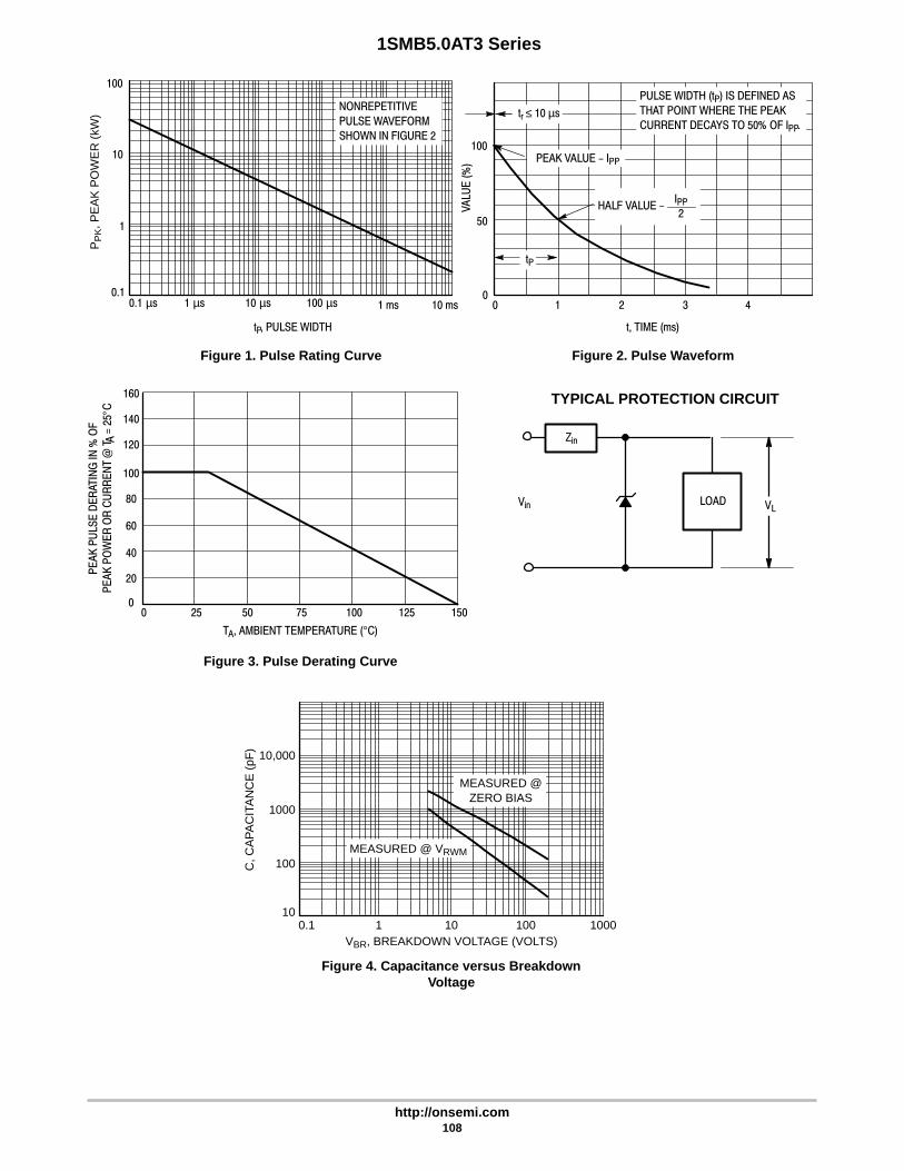
1SMB5.0AT3 Series
http://onsemi.com108
NONREPETITIVE
PULSE WAVEFORM
SHOWN IN FIGURE 2
tP, PULSE WIDTH
1
10
100
0.1 µs 1 µs 10 µs 100 µs 1 ms 10 ms0.1
Figure 1. Pulse Rating Curve
0 1 2 3 40
50
100
t, TIME (ms)
VA
LUE
(%
)
HALF VALUE -IPP
2
PEAK VALUE - IPP
tr≤ 10 µs
Figure 2. Pulse Waveform
TYPICAL PROTECTION CIRCUIT
Vin VL
Zin
LOAD
Figure 3. Pulse Derating Curve
PE
AK
PU
LSE
DE
RAT
ING
IN %
OF
PE
AK
PO
WE
R O
R C
UR
RE
NT
@ T
A=
25C°
100
80
60
40
20
00 25 50 75 100 125 150
TA, AMBIENT TEMPERATURE (°C)
120
140
160
tP
PULSE WIDTH (tP) IS DEFINED AS
THAT POINT WHERE THE PEAK
CURRENT DECAYS TO 50% OF IPP.
VBR, BREAKDOWN VOLTAGE (VOLTS)
Figure 4. Capacitance versus BreakdownVoltage
0.1 1 10 100 100010
100
1000
10,000
C, C
AP
AC
ITA
NC
E (
pF)
MEASURED @ZERO BIAS
MEASURED @ VRWM
PP
K, P
EA
K P
OW
ER
(kW
)

1SMB5.0AT3 Series
http://onsemi.com109
APPLICATION NOTES
RESPONSE TIMEIn most applications, the transient suppressor device is
placed in parallel with the equipment or component to beprotected. In this situation, there is a time delay associatedwith the capacitance of the device and an overshootcondition associated with the inductance of the device andthe inductance of the connection method. The capacitiveeffect is of minor importance in the parallel protectionscheme because it only produces a time delay in thetransition from the operating voltage to the clamp voltage asshown in Figure 5.
The inductive effects in the device are due to actualturn-on time (time required for the device to go from zerocurrent to full current) and lead inductance. This inductiveeffect produces an overshoot in the voltage across theequipment or component being protected as shown inFigure 6. Minimizing this overshoot is very important in theapplication, since the main purpose for adding a transientsuppressor is to clamp voltage spikes. The SMB series havea very good response time, typically < 1 ns and negligibleinductance. However, external inductive effects couldproduce unacceptable overshoot. Proper circuit layout,
minimum lead lengths and placing the suppressor device asclose as possible to the equipment or components to beprotected will minimize this overshoot.
Some input impedance represented by Zin is essential toprevent overstress of the protection device. This impedanceshould be as high as possible, without restricting the circuitoperation.
DUTY CYCLE DERATINGThe data of Figure 1 applies for non-repetitive conditions
and at a lead temperature of 25°C. If the duty cycle increases,the peak power must be reduced as indicated by the curvesof Figure 7. Average power must be derated as the lead orambient temperature rises above 25°C. The average powerderating curve normally given on data sheets may benormalized and used for this purpose.
At first glance the derating curves of Figure 7 appear to bein error as the 10 ms pulse has a higher derating factor thanthe 10 µs pulse. However, when the derating factor for agiven pulse of Figure 7 is multiplied by the peak power valueof Figure 1 for the same pulse, the results follow theexpected trend.

1SMB5.0AT3 Series
http://onsemi.com110
VL
V
Vin
Vin (TRANSIENT)VL
td
V
Vin (TRANSIENT)OVERSHOOT DUE TOINDUCTIVE EFFECTS
tD = TIME DELAY DUE TO CAPACITIVE EFFECT
t t
Figure 5. Figure 6.
Figure 7. Typical Derating Factor for Duty Cycle
DE
RA
TIN
G F
AC
TO
R
1 ms
10 µs
10.7
0.5
0.3
0.05
0.1
0.2
0.01
0.02
0.03
0.07
100 µs
0.1 0.2 0.5 2 5 10 501 20 100D, DUTY CYCLE (%)
PULSE WIDTH10 ms
UL RECOGNITION
The entire series has Underwriters LaboratoryRecognition for the classification of protectors (QVGV2)under the UL standard for safety 497B and File #116110.Many competitors only have one or two devices recognizedor have recognition in a non-protective category. Somecompetitors have no recognition at all. With the UL497Brecognition, our parts successfully passed several tests
including Strike Voltage Breakdown test, EnduranceConditioning, Temperature test, DielectricVoltage-Withstand test, Discharge test and several more.
Whereas, some competitors have only passed aflammability test for the package material, we have beenrecognized for much more to be included in their Protectorcategory.

Semiconductor Components Industries, LLC, 2001
May, 2001 – Rev. 5111 Publication Order Number:
P6SMB6.8AT3/D
P6SMB6.8AT3 Series
600 Watt Peak Power ZenerTransient Voltage Suppressors
Unidirectional*The SMB series is designed to protect voltage sensitive
components from high voltage, high energy transients. They haveexcellent clamping capability, high surge capability, low zenerimpedance and fast response time. The SMB series is supplied inON Semiconductor’s exclusive, cost-effective, highly reliableSurmetic package and is ideally suited for use in communicationsystems, automotive, numerical controls, process controls, medicalequipment, business machines, power supplies and many otherindustrial/consumer applications.
Specification Features:• Working Peak Reverse Voltage Range – 5.8 to 171 V
• Standard Zener Breakdown Voltage Range – 6.8 to 200 V
• Peak Power – 600 Watts @ 1 ms
• ESD Rating of Class 3 (>16 KV) per Human Body Model
• Maximum Clamp Voltage @ Peak Pulse Current
• Low Leakage < 5 µA Above 10 V
• UL 497B for Isolated Loop Circuit Protection
• Response Time is Typically < 1 ns
Mechanical Characteristics:CASE: Void-free, transfer-molded, thermosetting plasticFINISH: All external surfaces are corrosion resistant and leads are
readily solderableMAXIMUM CASE TEMPERATURE FOR SOLDERING PURPOSES:
260°C for 10 SecondsLEADS: Modified L–Bend providing more contact area to bond padsPOLARITY: Cathode indicated by polarity bandMOUNTING POSITION: Any
MAXIMUM RATINGS
Please See the Table on the Following Page
*Please see P6SMB11CAT3 to P6SMB91CAT3 for Bidirectional devices.
PLASTIC SURFACE MOUNTZENER OVERVOLTAGE
TRANSIENT SUPPRESSORS5.8–171 VOLTS
600 WATT PEAK POWER
Devices listed in bold, italic are ON SemiconductorPreferred devices. Preferred devices are recommendedchoices for future use and best overall value.
Device Package Shipping
ORDERING INFORMATION
P6SMBxxxAT3 SMB 2500/Tape & Reel
SMBCASE 403A
PLASTIC
http://onsemi.com
Cathode Anode
Y = YearWW = Work WeekxxxA = Specific Device Code
= (See Table on Page113)
YWWxxxA
MARKING DIAGRAM
†The “T3” suffix refers to a 13 inch reel.

Uni–Directional TVS
IPP
IF
V
I
IRIT
VRWMVC VBRVF
P6SMB6.8AT3 Series
http://onsemi.com112
MAXIMUM RATINGS
Rating Symbol Value Unit
Peak Power Dissipation (Note 1.) @ TL = 25°C, Pulse Width = 1 ms PPK 600 W
DC Power Dissipation @ TL = 75°CMeasured Zero Lead Length (Note 2.)Derate Above 75°C
Thermal Resistance from Junction to Lead
PD
RJL
3.0
4025
W
mW/°C°C/W
DC Power Dissipation (Note 3.) @ TA = 25°CDerate Above 25°C
Thermal Resistance from Junction to Ambient
PD
RJA
0.554.4226
WmW/°C°C/W
Forward Surge Current (Note 4.) @ TA = 25°C IFSM 100 A
Operating and Storage Temperature Range TJ, Tstg –65 to +150 °C
1. 10 X 1000 s, non–repetitive2. 1″ square copper pad, FR–4 board3. FR–4 board, using ON Semiconductor minimum recommended footprint, as shown in 403A case outline dimensions spec.4. 1/2 sine wave (or equivalent square wave), PW = 8.3 ms, duty cycle = 4 pulses per minute maximum.
ELECTRICAL CHARACTERISTICS(TA = 25°C unless otherwise noted, VF = 3.5 V Max. @IF (Note 4) = 30 A) (Note 5.)
Symbol Parameter
IPP Maximum Reverse Peak Pulse Current
VC Clamping Voltage @ IPP
VRWM Working Peak Reverse Voltage
IR Maximum Reverse Leakage Current @ VRWM
VBR Breakdown Voltage @ IT
IT Test Current
VBR Maximum Temperature Coefficient of VBR
IF Forward Current
VF Forward Voltage @ IF
5. 1/2 sine wave or equivalent, PW = 8.3 ms, non–repetitiveduty cycle

P6SMB6.8AT3 Series
http://onsemi.com113
ELECTRICAL CHARACTERISTICS (Devices listed in bold, italic are ON Semiconductor Preferred devices.)
VRWMBreakdown Voltage VC @ IPP (Note 8.)
Device
VRWM(Note 6.) IR @ VRWM VBR Volts (Note 7.) @ IT VC IPP VBR
DeviceDevice
Marking Volts µA Min Nom Max mA Volts Amps %/°C
P6SMB6.8AT3P6SMB7.5AT3P6SMB8.2AT3P6SMB9.1AT3
6V8A7V5A8V2A9V1A
5.86.47.027.78
100050020050
6.457.137.798.65
6.87.518.29.1
7.147.888.619.55
1010101
10.511.312.113.4
57535045
0.0570.0610.0650.068
P6SMB10AT3P6SMB11AT3P6SMB12AT3P6SMB13AT3
10A11A12A13A
8.559.410.211.1
10555
9.510.511.412.4
1011.05
1213.05
10.511.612.613.7
1111
14.515.616.718.2
41383633
0.0730.0750.0780.081
P6SMB15AT3P6SMB16AT3P6SMB18AT3P6SMB20AT3
15A16A18A20A
12.813.615.317.1
5555
14.315.217.119
15.05161820
15.816.818.921
1111
21.222.525.227.7
28272422
0.0840.0860.0880.09
P6SMB22AT3P6SMB24AT3P6SMB27AT3P6SMB30AT3
22A24A27A30A
18.820.523.125.6
5555
20.922.825.728.5
2224
27.0530
23.125.228.431.5
1111
30.633.237.541.4
201816
14.4
0.0920.0940.0960.097
P6SMB33AT3P6SMB36AT3P6SMB39AT3P6SMB43AT3
33A36A39A43A
28.230.833.336.8
5555
31.434.237.140.9
33.0536
39.0543.05
34.737.841
45.2
1111
45.749.953.959.3
13.212
11.210.1
0.0980.0990.1
0.101
P6SMB47AT3P6SMB51AT3P6SMB56AT3P6SMB62AT3
47A51A56A62A
40.243.647.853
5555
44.748.553.258.9
47.0551.05
5662
49.453.658.865.1
1111
64.870.17785
9.38.67.87.1
0.1010.1020.1030.104
P6SMB68AT3P6SMB75AT3P6SMB82AT3P6SMB91AT3
68A75A82A91A
58.164.170.177.8
5555
64.671.377.986.5
6875.05
8291
71.478.886.195.5
1111
92103113125
6.55.85.34.8
0.1040.1050.1050.106
P6SMB100AT3P6SMB110AT3P6SMB120AT3P6SMB130AT3
100A110A120A130A
85.594102111
5555
95105114124
100110.5120
130.5
105116126137
1111
137152165179
4.44.03.63.3
0.1060.1070.1070.107
P6SMB150AT3P6SMB160AT3P6SMB170AT3P6SMB180AT3
150A160A170A180A
128136145154
5555
143152162171
150.5160170180
158168179189
1111
207219234246
2.92.72.62.4
0.1080.1080.1080.108
P6SMB200AT3 200A 171 5 190 200 210 1 274 2.2 0.108
6. A transient suppressor is normally selected according to the working peak reverse voltage (VRWM), which should be equal to or greater thanthe DC or continuous peak operating voltage level.
7. VBR measured at pulse test current IT at an ambient temperature of 25°C.8. Surge current waveform per Figure 2 and derate per Figure 3.

P6SMB6.8AT3 Series
http://onsemi.com114
P ,
PE
AK
PO
WE
R (
kW)
PNONREPETITIVE
PULSE WAVEFORM
SHOWN IN FIGURE 2
tP, PULSE WIDTH
1
10
100
0.1 µs 1 µs 10 µs 100 µs 1 ms 10 ms0.1
Figure 1. Pulse Rating Curve
0 1 2 3 40
50
100
t, TIME (ms)
VA
LUE
(%
)
HALF VALUE -IPP
2
PEAK VALUE - IPP
tr≤ 10 µs
Figure 2. Pulse Waveform
TYPICAL PROTECTION CIRCUIT
Vin VL
Zin
LOAD
Figure 3. Pulse Derating Curve
PE
AK
PU
LSE
DE
RAT
ING
IN %
OF
PE
AK
PO
WE
R O
R C
UR
RE
NT
@ T
A=
25C°
100
80
60
40
20
00 25 50 75 100 125 150
TA, AMBIENT TEMPERATURE (°C)
120
140
160
tP
PULSE WIDTH (tP) IS DEFINED AS
THAT POINT WHERE THE PEAK
CURRENT DECAYS TO 50% OF IPP.
VBR, BREAKDOWN VOLTAGE (VOLTS)
Figure 4. Capacitance versus BreakdownVoltage
0.1 1 10 100 100010
100
1000
10,000
C, C
AP
AC
ITA
NC
E (
pF)
MEASURED @ZERO BIAS
MEASURED @ VRWM

P6SMB6.8AT3 Series
http://onsemi.com115
APPLICATION NOTES
RESPONSE TIMEIn most applications, the transient suppressor device is
placed in parallel with the equipment or component to beprotected. In this situation, there is a time delay associatedwith the capacitance of the device and an overshootcondition associated with the inductance of the device andthe inductance of the connection method. The capacitiveeffect is of minor importance in the parallel protectionscheme because it only produces a time delay in thetransition from the operating voltage to the clamp voltage asshown in Figure 5.
The inductive effects in the device are due to actualturn-on time (time required for the device to go from zerocurrent to full current) and lead inductance. This inductiveeffect produces an overshoot in the voltage across theequipment or component being protected as shown inFigure 6. Minimizing this overshoot is very important in theapplication, since the main purpose for adding a transientsuppressor is to clamp voltage spikes. The SMB series havea very good response time, typically < 1 ns and negligibleinductance. However, external inductive effects couldproduce unacceptable overshoot. Proper circuit layout,
minimum lead lengths and placing the suppressor device asclose as possible to the equipment or components to beprotected will minimize this overshoot.
Some input impedance represented by Zin is essential toprevent overstress of the protection device. This impedanceshould be as high as possible, without restricting the circuitoperation.
DUTY CYCLE DERATINGThe data of Figure 1 applies for non-repetitive conditions
and at a lead temperature of 25°C. If the duty cycle increases,the peak power must be reduced as indicated by the curvesof Figure 7. Average power must be derated as the lead orambient temperature rises above 25°C. The average powerderating curve normally given on data sheets may benormalized and used for this purpose.
At first glance the derating curves of Figure 7 appear to bein error as the 10 ms pulse has a higher derating factor thanthe 10 µs pulse. However, when the derating factor for agiven pulse of Figure 7 is multiplied by the peak power valueof Figure 1 for the same pulse, the results follow theexpected trend.

P6SMB6.8AT3 Series
http://onsemi.com116
VL
V
Vin
Vin (TRANSIENT)VL
td
V
Vin (TRANSIENT)OVERSHOOT DUE TOINDUCTIVE EFFECTS
tD = TIME DELAY DUE TO CAPACITIVE EFFECT
t t
Figure 5. Figure 6.
Figure 7. Typical Derating Factor for Duty Cycle
DE
RA
TIN
G F
AC
TO
R
1 ms
10 µs
10.7
0.5
0.3
0.05
0.1
0.2
0.01
0.02
0.03
0.07
100 µs
0.1 0.2 0.5 2 5 10 501 20 100D, DUTY CYCLE (%)
PULSE WIDTH10 ms
UL RECOGNITION
The entire series has Underwriters LaboratoryRecognition for the classification of protectors (QVGV2)under the UL standard for safety 497B and File #116110.Many competitors only have one or two devices recognizedor have recognition in a non-protective category. Somecompetitors have no recognition at all. With the UL497Brecognition, our parts successfully passed several tests
including Strike Voltage Breakdown test, EnduranceConditioning, Temperature test, DielectricVoltage-Withstand test, Discharge test and several more.
Whereas, some competitors have only passed aflammability test for the package material, we have beenrecognized for much more to be included in their Protectorcategory.

Semiconductor Components Industries, LLC, 2001
May, 2001 – Rev. 4117 Publication Order Number:
1SMB10CAT3/D
1SMB10CAT3 Series
600 Watt Peak Power ZenerTransient Voltage Suppressors
Bidirectional*The SMB series is designed to protect voltage sensitive
components from high voltage, high energy transients. They haveexcellent clamping capability, high surge capability, low zenerimpedance and fast response time. The SMB series is supplied inON Semiconductor’s exclusive, cost-effective, highly reliableSurmetic package and is ideally suited for use in communicationsystems, automotive, numerical controls, process controls, medicalequipment, business machines, power supplies and many otherindustrial/consumer applications.
Specification Features:• Working Peak Reverse Voltage Range – 10 V to 78 V
• Standard Zener Breakdown Voltage Range – 11.7 V to 91.3 V
• Peak Power – 600 Watts @ 1 ms
• ESD Rating of Class 3 (> 16 KV) per Human Body Model
• Maximum Clamp Voltage @ Peak Pulse Current
• Low Leakage < 5 µA Above 10 V
• UL 497B for Isolated Loop Circuit Protection
• Response Time is Typically < 1 ns
Mechanical Characteristics:CASE: Void-free, transfer-molded, thermosetting plasticFINISH: All external surfaces are corrosion resistant and leads are
readily solderableMAXIMUM CASE TEMPERATURE FOR SOLDERING PURPOSES:
260°C for 10 SecondsLEADS: Modified L–Bend providing more contact area to bond padsPOLARITY: Polarity band will not be indicatedMOUNTING POSITION: Any
MAXIMUM RATINGS
Rating Symbol Value Unit
Peak Power Dissipation (Note 1.)@ TL = 25°C, Pulse Width = 1 ms
PPK 600 W
DC Power Dissipation @ TL = 75°CMeasured Zero Lead Length (Note 2.)Derate Above 75°C
Thermal Resistance from Junction to Lead
PD
RJL
3.0
4025
W
mW/°C°C/W
DC Power Dissipation (Note 3.) @ TA = 25°CDerate Above 25°C
Thermal Resistance from Junctionto Ambient
PD
RJA
0.55
4.4226
W
mW/°C°C/W
Operating and StorageTemperature Range
TJ, Tstg –65 to+150
°C
1. 10 X 1000 s, non–repetitive2. 1″ square copper pad, FR–4 board3. FR–4 board, using ON Semiconductor minimum recommended footprint, as
shown in 403A case outline dimensions spec.
*Please see 1SMB5.0AT3 to 1SMB170AT3 for Unidirectional devices.
PLASTIC SURFACE MOUNTZENER OVERVOLTAGE
TRANSIENT SUPPRESSORS10–78 VOLTS
600 WATT PEAK POWER
Devices listed in bold, italic are ON SemiconductorPreferred devices. Preferred devices are recommendedchoices for future use and best overall value.
Device Package Shipping
ORDERING INFORMATION
1SMBxxCAT3 SMB 2500/Tape & Reel
SMBCASE 403A
PLASTIC
http://onsemi.com
Y = YearWW = Work WeekxxC = Specific Device Code
= (See Table Next Page)
YWWxxC
MARKING DIAGRAM
†The “T3” suffix refers to a 13 inch reel.

Bi–Directional TVS
IPP
IPP
V
I
IRIT
ITIRVRWMVC VBR
VRWM VCVBR
1SMB10CAT3 Series
http://onsemi.com118
ELECTRICAL CHARACTERISTICS(TA = 25°C unless otherwise noted)
Symbol Parameter
IPP Maximum Reverse Peak Pulse Current
VC Clamping Voltage @ IPP
VRWM Working Peak Reverse Voltage
IR Maximum Reverse Leakage Current @ VRWM
VBR Breakdown Voltage @ IT
IT Test Current
ELECTRICAL CHARACTERISTICS (Devices listed in bold, italic are ON Semiconductor Preferred devices.)
VRWMBreakdown Voltage VC @ IPP (Note 6.)
Device
VRWM(Note 4.) IR @ VRWM VBR (Note 5.) Volts @ IT VC IPP
DeviceDevice
Marking Volts µA Min Nom Max mA Volts Amps
1SMB10CAT31SMB11CAT31SMB12CAT31SMB13CAT3
KXCKZCLECLGC
10111213
5.05.05.05.0
11.112.213.314.4
11.6912.8414.0015.16
12.2713.514.715.9
1.01.01.01.0
17.018.219.921.5
35.333.030.227.9
1SMB14CAT31SMB15CAT31SMB16CAT31SMB17CAT3
LKCLMCLPCLRC
14151617
5.05.05.05.0
15.616.717.818.9
16.4217.5818.7419.90
17.218.519.720.9
1.01.01.01.0
23.224.426.027.6
25.824.023.121.7
1SMB18CAT31SMB20CAT31SMB22CAT31SMB24CAT3
LTCLVCLXCLZC
18202224
5.05.05.05.0
20.022.224.426.7
21.0623.3725.6928.11
22.124.527.029.5
1.01.01.01.0
29.232.435.538.9
20.518.516.915.4
1SMB26CAT31SMB28CAT31SMB30CAT31SMB33CAT3
MECMGCMKCMMC
26283033
5.05.05.05.0
28.931.133.336.7
30.4232.7435.0638.63
31.934.436.840.6
1.01.01.01.0
42.145.448.453.3
14.213.212.411.3
1SMB36CAT31SMB40CAT31SMB43CAT31SMB45CAT3
MPCMRCMTCMVC
36404345
5.05.05.05.0
40.044.447.850.0
42.1146.7450.3252.63
44.249.152.855.3
1.01.01.01.0
58.164.569.472.2
10.39.38.68.3
1SMB48CAT31SMB51CAT31SMB54CAT31SMB58CAT3
MXCMZCNECNGC
48515458
5.05.05.05.0
53.356.760.064.4
56.1159.6963.1667.79
58.962.766.3271.18
1.01.01.01.0
77.482.487.193.6
7.77.36.96.4
1SMB60CAT31SMB64CAT31SMB70CAT31SMB75CAT3
NKCNMCNPCNRC
60647075
5.05.05.05.0
66.771.177.883.3
70.2174.8481.9091.65
73.7278.5885.9992.07
1.01.01.01.0
96.8103113121
6.25.85.34.9
1SMB78CAT3 NTC 78 5.0 86.7 91.26 95.83 1.0 126 4.7
4. A transient suppressor is normally selected according to the working peak reverse voltage (VRWM), which should be equal to or greater thanthe DC or continuous peak operating voltage level.
5. VBR measured at pulse test current IT at an ambient temperature of 25°C.6. Surge current waveform per Figure 2 and derate per Figure 3 of the General Data – 600 Watt at the beginning of this group.

1SMB10CAT3 Series
http://onsemi.com119
NONREPETITIVE
PULSE WAVEFORM
SHOWN IN FIGURE 2
tP, PULSE WIDTH
1
10
100
0.1 µs 1 µs 10 µs 100 µs 1 ms 10 ms0.1
Figure 1. Pulse Rating Curve
0 1 2 3 40
50
100
t, TIME (ms)
VA
LUE
(%
)
HALF VALUE -IPP
2
PEAK VALUE - IPP
tr≤ 10 µs
Figure 2. Pulse Waveform
TYPICAL PROTECTION CIRCUIT
Vin VL
Zin
LOAD
Figure 3. Pulse Derating Curve
PE
AK
PU
LSE
DE
RAT
ING
IN %
OF
PE
AK
PO
WE
R O
R C
UR
RE
NT
@ T
A=
25C°
100
80
60
40
20
00 25 50 75 100 125 150
TA, AMBIENT TEMPERATURE (°C)
120
140
160
tP
PULSE WIDTH (tP) IS DEFINED
AS THAT POINT WHERE THE PEAK
CURRENT DECAYS TO 50% OF IPP.
PP
K, P
EA
K P
OW
ER
(kW
)
1SMB10CAT3 Series
http://onsemi.com120
APPLICATION NOTES
RESPONSE TIMEIn most applications, the transient suppressor device is
placed in parallel with the equipment or component to beprotected. In this situation, there is a time delay associatedwith the capacitance of the device and an overshootcondition associated with the inductance of the device andthe inductance of the connection method. The capacitiveeffect is of minor importance in the parallel protectionscheme because it only produces a time delay in thetransition from the operating voltage to the clamp voltage asshown in Figure 4.
The inductive effects in the device are due to actualturn-on time (time required for the device to go from zerocurrent to full current) and lead inductance. This inductiveeffect produces an overshoot in the voltage across theequipment or component being protected as shown inFigure 5. Minimizing this overshoot is very important in theapplication, since the main purpose for adding a transientsuppressor is to clamp voltage spikes. The SMB series havea very good response time, typically < 1 ns and negligibleinductance. However, external inductive effects couldproduce unacceptable overshoot. Proper circuit layout,
minimum lead lengths and placing the suppressor device asclose as possible to the equipment or components to beprotected will minimize this overshoot.
Some input impedance represented by Zin is essential toprevent overstress of the protection device. This impedanceshould be as high as possible, without restricting the circuitoperation.
DUTY CYCLE DERATINGThe data of Figure 1 applies for non-repetitive conditions
and at a lead temperature of 25°C. If the duty cycle increases,the peak power must be reduced as indicated by the curvesof Figure 6. Average power must be derated as the lead orambient temperature rises above 25°C. The average powerderating curve normally given on data sheets may benormalized and used for this purpose.
At first glance the derating curves of Figure 6 appear to bein error as the 10 ms pulse has a higher derating factor thanthe 10 µs pulse. However, when the derating factor for agiven pulse of Figure 6 is multiplied by the peak power valueof Figure 1 for the same pulse, the results follow theexpected trend.

1SMB10CAT3 Series
http://onsemi.com121
VL
V
Vin
Vin (TRANSIENT)VL
td
V
Vin (TRANSIENT)OVERSHOOT DUE TOINDUCTIVE EFFECTS
tD = TIME DELAY DUE TO CAPACITIVE EFFECT
t t
Figure 4. Figure 5.
Figure 6. Typical Derating Factor for Duty Cycle
DE
RA
TIN
G F
AC
TO
R
1 ms
10 µs
10.7
0.5
0.3
0.05
0.1
0.2
0.01
0.02
0.03
0.07
100 µs
0.1 0.2 0.5 2 5 10 501 20 100D, DUTY CYCLE (%)
PULSE WIDTH10 ms
UL RECOGNITION
The entire series has Underwriters LaboratoryRecognition for the classification of protectors (QVGV2)under the UL standard for safety 497B and File #116110.Many competitors only have one or two devices recognizedor have recognition in a non-protective category. Somecompetitors have no recognition at all. With the UL497Brecognition, our parts successfully passed several tests
including Strike Voltage Breakdown test, EnduranceConditioning, Temperature test, DielectricVoltage-Withstand test, Discharge test and several more.
Whereas, some competitors have only passed aflammability test for the package material, we have beenrecognized for much more to be included in their Protectorcategory.

Semiconductor Components Industries, LLC, 2001
May, 2001 – Rev. 4122 Publication Order Number:
P6SMB11CAT3/D
P6SMB11CAT3 Series
600 Watt Peak Power ZenerTransient Voltage Suppressors
Bidirectional*The SMB series is designed to protect voltage sensitive
components from high voltage, high energy transients. They haveexcellent clamping capability, high surge capability, low zenerimpedance and fast response time. The SMB series is supplied inON Semiconductor’s exclusive, cost-effective, highly reliableSurmetic package and is ideally suited for use in communicationsystems, automotive, numerical controls, process controls, medicalequipment, business machines, power supplies and many otherindustrial/consumer applications.
Specification Features:• Working Peak Reverse Voltage Range – 9.4 to 77.8 V
• Standard Zener Breakdown Voltage Range – 11 to 91 V
• Peak Power – 600 Watts @ 1 ms
• ESD Rating of Class 3 (>16 KV) per Human Body Model
• Maximum Clamp Voltage @ Peak Pulse Current
• Low Leakage < 5 µA Above 10 V
• UL 497B for Isolated Loop Circuit Protection
• Response Time is Typically < 1 ns
Mechanical Characteristics:CASE: Void-free, transfer-molded, thermosetting plasticFINISH: All external surfaces are corrosion resistant and leads are
readily solderableMAXIMUM CASE TEMPERATURE FOR SOLDERING PURPOSES:
260°C for 10 SecondsLEADS: Modified L–Bend providing more contact area to bond padsPOLARITY: Polarity band will not be indicatedMOUNTING POSITION: Any
MAXIMUM RATINGS
Rating Symbol Value Unit
Peak Power Dissipation (Note 1.)@ TL = 25°C, Pulse Width = 1 ms
PPK 600 W
DC Power Dissipation @ TL = 75°CMeasured Zero Lead Length (Note 2.)Derate Above 75°C
Thermal Resistance from Junction to Lead
PD
RJL
3.0
4025
W
mW/°C°C/W
DC Power Dissipation (Note 3.) @ TA = 25°CDerate Above 25°C
Thermal Resistance from Junctionto Ambient
PD
RJA
0.55
4.4226
W
mW/°C°C/W
Operating and StorageTemperature Range
TJ, Tstg –65 to+150
°C
1. 10 X 1000 s, non–repetitive2. 1″ square copper pad, FR–4 board3. FR–4 board, using ON Semiconductor minimum recommended footprint, as
shown in 403A case outline dimensions spec.
*Please see P6SMB6.8AT3 to P6SMB200AT3 for Unidirectional devices.
PLASTIC SURFACE MOUNTZENER OVERVOLTAGE
TRANSIENT SUPPRESSORS9.4–78 VOLTS
600 WATT PEAK POWER
Devices listed in bold, italic are ON SemiconductorPreferred devices. Preferred devices are recommendedchoices for future use and best overall value.
Device Package Shipping
ORDERING INFORMATION
P6SMBxxCAT3 SMB 2500/Tape & Reel
SMBCASE 403A
PLASTIC
http://onsemi.com
Y = YearWW = Work WeekxxC = Specific Device Code
= (See Table Next Page)
YWWxxC
MARKING DIAGRAM
†The “T3” suffix refers to a 13 inch reel.
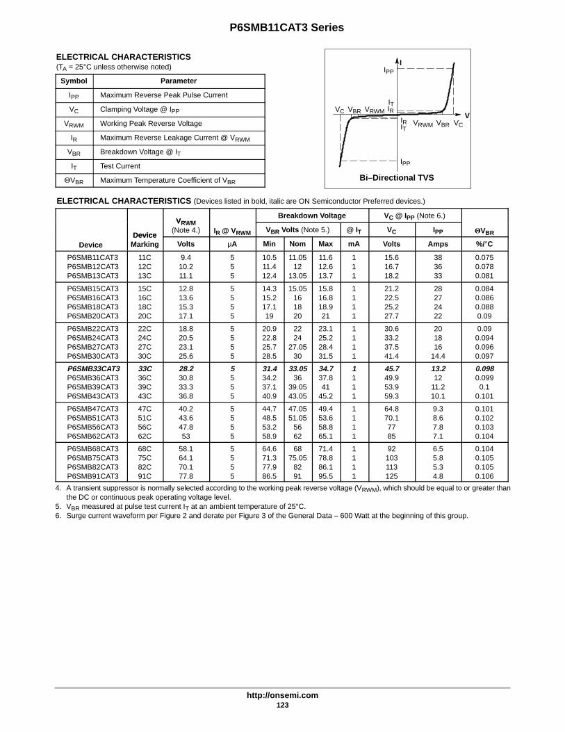
Bi–Directional TVS
IPP
IPP
V
I
IRIT
ITIRVRWMVC VBR
VRWM VCVBR
P6SMB11CAT3 Series
http://onsemi.com123
ELECTRICAL CHARACTERISTICS(TA = 25°C unless otherwise noted)
Symbol Parameter
IPP Maximum Reverse Peak Pulse Current
VC Clamping Voltage @ IPP
VRWM Working Peak Reverse Voltage
IR Maximum Reverse Leakage Current @ VRWM
VBR Breakdown Voltage @ IT
IT Test Current
VBR Maximum Temperature Coefficient of VBR
ELECTRICAL CHARACTERISTICS (Devices listed in bold, italic are ON Semiconductor Preferred devices.)
VRWMBreakdown Voltage VC @ IPP (Note 6.)
Device
VRWM(Note 4.) IR @ VRWM VBR Volts (Note 5.) @ IT VC IPP VBR
DeviceDevice
Marking Volts µA Min Nom Max mA Volts Amps %/°C
P6SMB11CAT3P6SMB12CAT3P6SMB13CAT3
11C12C13C
9.410.211.1
555
10.511.412.4
11.0512
13.05
11.612.613.7
111
15.616.718.2
383633
0.0750.0780.081
P6SMB15CAT3P6SMB16CAT3P6SMB18CAT3P6SMB20CAT3
15C16C18C20C
12.813.615.317.1
5555
14.315.217.119
15.05161820
15.816.818.921
1111
21.222.525.227.7
28272422
0.0840.0860.0880.09
P6SMB22CAT3P6SMB24CAT3P6SMB27CAT3P6SMB30CAT3
22C24C27C30C
18.820.523.125.6
5555
20.922.825.728.5
2224
27.0530
23.125.228.431.5
1111
30.633.237.541.4
201816
14.4
0.090.0940.0960.097
P6SMB33CAT3P6SMB36CAT3P6SMB39CAT3P6SMB43CAT3
33C36C39C43C
28.230.833.336.8
5555
31.434.237.140.9
33.0536
39.0543.05
34.737.841
45.2
1111
45.749.953.959.3
13.212
11.210.1
0.0980.0990.1
0.101
P6SMB47CAT3P6SMB51CAT3P6SMB56CAT3P6SMB62CAT3
47C51C56C62C
40.243.647.853
5555
44.748.553.258.9
47.0551.05
5662
49.453.658.865.1
1111
64.870.17785
9.38.67.87.1
0.1010.1020.1030.104
P6SMB68CAT3P6SMB75CAT3P6SMB82CAT3P6SMB91CAT3
68C75C82C91C
58.164.170.177.8
5555
64.671.377.986.5
6875.05
8291
71.478.886.195.5
1111
92103113125
6.55.85.34.8
0.1040.1050.1050.106
4. A transient suppressor is normally selected according to the working peak reverse voltage (VRWM), which should be equal to or greater thanthe DC or continuous peak operating voltage level.
5. VBR measured at pulse test current IT at an ambient temperature of 25°C.6. Surge current waveform per Figure 2 and derate per Figure 3 of the General Data – 600 Watt at the beginning of this group.

P6SMB11CAT3 Series
http://onsemi.com124
P ,
PE
AK
PO
WE
R (
kW)
PNONREPETITIVE
PULSE WAVEFORM
SHOWN IN FIGURE 2
tP, PULSE WIDTH
1
10
100
0.1 µs 1 µs 10 µs 100 µs 1 ms 10 ms0.1
Figure 1. Pulse Rating Curve
0 1 2 3 40
50
100
t, TIME (ms)
VA
LUE
(%
)
HALF VALUE -IPP
2
PEAK VALUE - IPP
tr≤ 10 µs
Figure 2. Pulse Waveform
TYPICAL PROTECTION CIRCUIT
Vin VL
Zin
LOAD
Figure 3. Pulse Derating Curve
PE
AK
PU
LSE
DE
RAT
ING
IN %
OF
PE
AK
PO
WE
R O
R C
UR
RE
NT
@ T
A=
25C°
100
80
60
40
20
00 25 50 75 100 125 150
TA, AMBIENT TEMPERATURE (°C)
120
140
160
tP
PULSE WIDTH (tP) IS DEFINED AS
THAT POINT WHERE THE PEAK
CURRENT DECAYS TO 50% OF IPP.

P6SMB11CAT3 Series
http://onsemi.com125
APPLICATION NOTES
RESPONSE TIMEIn most applications, the transient suppressor device is
placed in parallel with the equipment or component to beprotected. In this situation, there is a time delay associatedwith the capacitance of the device and an overshootcondition associated with the inductance of the device andthe inductance of the connection method. The capacitiveeffect is of minor importance in the parallel protectionscheme because it only produces a time delay in thetransition from the operating voltage to the clamp voltage asshown in Figure 4.
The inductive effects in the device are due to actualturn-on time (time required for the device to go from zerocurrent to full current) and lead inductance. This inductiveeffect produces an overshoot in the voltage across theequipment or component being protected as shown inFigure 5. Minimizing this overshoot is very important in theapplication, since the main purpose for adding a transientsuppressor is to clamp voltage spikes. The SMB series havea very good response time, typically < 1 ns and negligibleinductance. However, external inductive effects couldproduce unacceptable overshoot. Proper circuit layout,
minimum lead lengths and placing the suppressor device asclose as possible to the equipment or components to beprotected will minimize this overshoot.
Some input impedance represented by Zin is essential toprevent overstress of the protection device. This impedanceshould be as high as possible, without restricting the circuitoperation.
DUTY CYCLE DERATINGThe data of Figure 1 applies for non-repetitive conditions
and at a lead temperature of 25°C. If the duty cycle increases,the peak power must be reduced as indicated by the curvesof Figure 6. Average power must be derated as the lead orambient temperature rises above 25°C. The average powerderating curve normally given on data sheets may benormalized and used for this purpose.
At first glance the derating curves of Figure 6 appear to bein error as the 10 ms pulse has a higher derating factor thanthe 10 µs pulse. However, when the derating factor for agiven pulse of Figure 6 is multiplied by the peak power valueof Figure 1 for the same pulse, the results follow theexpected trend.

P6SMB11CAT3 Series
http://onsemi.com126
VL
V
Vin
Vin (TRANSIENT)VL
td
V
Vin (TRANSIENT)OVERSHOOT DUE TOINDUCTIVE EFFECTS
tD = TIME DELAY DUE TO CAPACITIVE EFFECT
t t
Figure 4. Figure 5.
Figure 6. Typical Derating Factor for Duty Cycle
DE
RA
TIN
G F
AC
TO
R
1 ms
10 µs
10.7
0.5
0.3
0.05
0.1
0.2
0.01
0.02
0.03
0.07
100 µs
0.1 0.2 0.5 2 5 10 501 20 100D, DUTY CYCLE (%)
PULSE WIDTH10 ms
UL RECOGNITION
The entire series has Underwriters LaboratoryRecognition for the classification of protectors (QVGV2)under the UL standard for safety 497B and File #116110.Many competitors only have one or two devices recognizedor have recognition in a non-protective category. Somecompetitors have no recognition at all. With the UL497Brecognition, our parts successfully passed several tests
including Strike Voltage Breakdown test, EnduranceConditioning, Temperature test, DielectricVoltage-Withstand test, Discharge test and several more.
Whereas, some competitors have only passed aflammability test for the package material, we have beenrecognized for much more to be included in their Protectorcategory.

Semiconductor Components Industries, LLC, 2001
May, 2001 – Rev. 3127 Publication Order Number:
1SMC5.0AT3/D
1SMC5.0AT3 Series
1500 Watt Peak Power ZenerTransient Voltage Suppressors
Unidirectional*The SMC series is designed to protect voltage sensitive
components from high voltage, high energy transients. They haveexcellent clamping capability, high surge capability, low zenerimpedance and fast response time. The SMC series is supplied inON Semiconductor’s exclusive, cost-effective, highly reliableSurmetic package and is ideally suited for use in communicationsystems, automotive, numerical controls, process controls, medicalequipment, business machines, power supplies and many otherindustrial/consumer applications.
Specification Features:• Working Peak Reverse Voltage Range – 5.0 V to 78 V
• Standard Zener Breakdown Voltage Range – 6.7 V to 91.25 V
• Peak Power – 1500 Watts @ 1 ms
• ESD Rating of Class 3 (>16 KV) per Human Body Model
• Maximum Clamp Voltage @ Peak Pulse Current
• Low Leakage < 5 µA Above 10 V
• UL 497B for Isolated Loop Circuit Protection
• Maximum Temperature Coefficient Specified
• Response Time is Typically < 1 ns
Mechanical Characteristics:CASE: Void-free, transfer-molded, thermosetting plasticFINISH: All external surfaces are corrosion resistant and leads are
readily solderableMAXIMUM CASE TEMPERATURE FOR SOLDERING PURPOSES:
260°C for 10 SecondsLEADS: Modified L–Bend providing more contact area to bond padsPOLARITY: Cathode indicated by molded polarity notchMOUNTING POSITION: Any
MAXIMUM RATINGS
Please See the Table on the Following Page
PLASTIC SURFACE MOUNTZENER TRANSIENT
VOLTAGE SUPPRESSORS5.0–78 VOLTS
1500 WATT PEAK POWER
Device Package Shipping
ORDERING INFORMATION
1SMCxxxAT3 SMC 2500/Tape & Reel
SMCCASE 403PLASTIC
http://onsemi.com
Cathode Anode
Y = YearWW = Work WeekGxx = Specific Device Code
= (See Table on Page129)
YWWGxx
MARKING DIAGRAM
*Bidirectional devices will not be available in thisseries.
†The “T3” suffix refers to a 13 inch reel.
Devices listed in bold, italic are ON SemiconductorPreferred devices. Preferred devices are recommendedchoices for future use and best overall value.

Uni–Directional TVS
IPP
IF
V
I
IRIT
VRWMVC VBRVF
1SMC5.0AT3 Series
http://onsemi.com128
MAXIMUM RATINGS
Rating Symbol Value Unit
Peak Power Dissipation (Note 1.) @ TL = 25°C, Pulse Width = 1 ms PPK 1500 W
DC Power Dissipation @ TL = 75°CMeasured Zero Lead Length (Note 2.)Derate Above 75°C
Thermal Resistance from Junction to Lead
PD
RJL
4.0
54.618.3
W
mW/°C°C/W
DC Power Dissipation (Note 3.) @ TA = 25°CDerate Above 25°C
Thermal Resistance from Junction to Ambient
PD
RJA
0.756.1165
WmW/°C°C/W
Forward Surge Current (Note 4.) @ TA = 25°C IFSM 200 A
Operating and Storage Temperature Range TJ, Tstg –65 to +150 °C
1. 10 X 1000 s, non–repetitive2. 1″ square copper pad, FR–4 board3. FR–4 board, using ON Semiconductor minimum recommended footprint, as shown in 403 case outline dimensions spec.4. 1/2 sine wave (or equivalent square wave), PW = 8.3 ms, duty cycle = 4 pulses per minute maximum.
ELECTRICAL CHARACTERISTICS (TA = 25°C unlessotherwise noted, VF = 3.5 V Max @ IF = 100 A) (Note 5.)
Symbol Parameter
IPP Maximum Reverse Peak Pulse Current
VC Clamping Voltage @ IPP
VRWM Working Peak Reverse Voltage
IR Maximum Reverse Leakage Current @ VRWM
VBR Breakdown Voltage @ IT
IT Test Current
IF Forward Current
VF Forward Voltage @ IF
5. 1/2 sine wave or equivalent, PW = 8.3 msnon–repetitive duty cycle
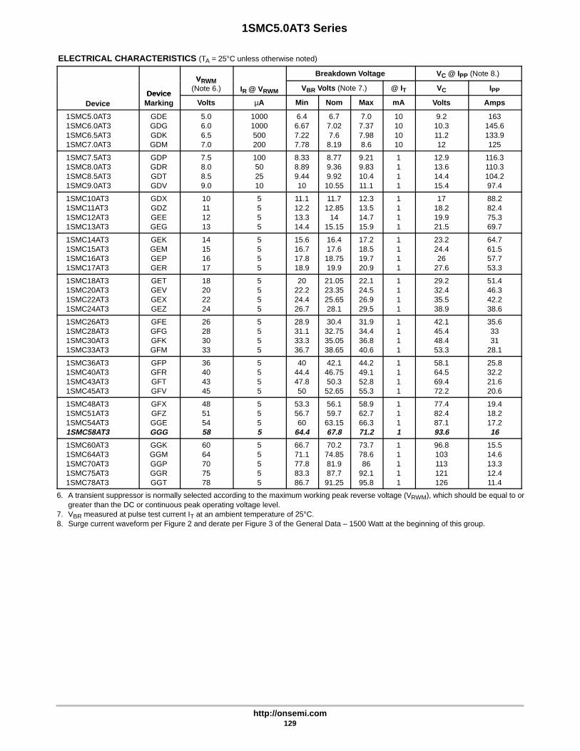
1SMC5.0AT3 Series
http://onsemi.com129
ELECTRICAL CHARACTERISTICS (TA = 25°C unless otherwise noted)
VRWMBreakdown Voltage VC @ IPP (Note 8.)
Device
VRWM(Note 6.) IR @ VRWM VBR Volts (Note 7.) @ IT VC IPP
DeviceDevice
Marking Volts µA Min Nom Max mA Volts Amps
1SMC5.0AT31SMC6.0AT31SMC6.5AT31SMC7.0AT3
GDEGDGGDKGDM
5.06.06.57.0
10001000500200
6.46.677.227.78
6.77.027.68.19
7.07.377.988.6
10101010
9.210.311.212
163145.6133.9125
1SMC7.5AT31SMC8.0AT31SMC8.5AT31SMC9.0AT3
GDPGDRGDTGDV
7.58.08.59.0
100502510
8.338.899.4410
8.779.369.9210.55
9.219.8310.411.1
1111
12.913.614.415.4
116.3110.3104.297.4
1SMC10AT31SMC11AT31SMC12AT31SMC13AT3
GDXGDZGEEGEG
10111213
5555
11.112.213.314.4
11.712.85
1415.15
12.313.514.715.9
1111
1718.219.921.5
88.282.475.369.7
1SMC14AT31SMC15AT31SMC16AT31SMC17AT3
GEKGEMGEPGER
14151617
5555
15.616.717.818.9
16.417.618.7519.9
17.218.519.720.9
1111
23.224.426
27.6
64.761.557.753.3
1SMC18AT31SMC20AT31SMC22AT31SMC24AT3
GETGEVGEXGEZ
18202224
5555
2022.224.426.7
21.0523.3525.6528.1
22.124.526.929.5
1111
29.232.435.538.9
51.446.342.238.6
1SMC26AT31SMC28AT31SMC30AT31SMC33AT3
GFEGFGGFKGFM
26283033
5555
28.931.133.336.7
30.432.7535.0538.65
31.934.436.840.6
1111
42.145.448.453.3
35.63331
28.1
1SMC36AT31SMC40AT31SMC43AT31SMC45AT3
GFPGFRGFTGFV
36404345
5555
4044.447.850
42.146.7550.352.65
44.249.152.855.3
1111
58.164.569.472.2
25.832.221.620.6
1SMC48AT31SMC51AT31SMC54AT31SMC58AT3
GFXGFZGGEGGG
48515458
5555
53.356.760
64.4
56.159.763.1567.8
58.962.766.371.2
1111
77.482.487.193.6
19.418.217.216
1SMC60AT31SMC64AT31SMC70AT31SMC75AT31SMC78AT3
GGKGGMGGPGGRGGT
6064707578
55555
66.771.177.883.386.7
70.274.8581.987.791.25
73.778.686
92.195.8
11111
96.8103113121126
15.514.613.312.411.4
6. A transient suppressor is normally selected according to the maximum working peak reverse voltage (VRWM), which should be equal to orgreater than the DC or continuous peak operating voltage level.
7. VBR measured at pulse test current IT at an ambient temperature of 25°C.8. Surge current waveform per Figure 2 and derate per Figure 3 of the General Data – 1500 Watt at the beginning of this group.

1SMC5.0AT3 Series
http://onsemi.com130
NONREPETITIVE
PULSE WAVEFORM
SHOWN IN FIGURE 2
tP, PULSE WIDTH
1
10
100
0.1 µs 1 µs 10 µs 100 µs 1 ms 10 ms
Figure 1. Pulse Rating Curve
0 1 2 3 40
50
100
t, TIME (ms)
VA
LUE
(%
)
HALF VALUE -IPP
2
PEAK VALUE - IPP
Figure 2. Pulse Waveform
Figure 3. Pulse Derating Curve
PE
AK
PU
LSE
DE
RAT
ING
IN %
OF
PE
AK
PO
WE
R O
R C
UR
RE
NT
@ T
A=
25C°
100
80
60
40
20
00 25 50 75 100 125 150
TA, AMBIENT TEMPERATURE (°C)
120
140
160
tP
PULSE WIDTH (tP) IS DEFINED
AS THAT POINT WHERE THE PEAK
CURRENT DECAYS TO 50%
OF IPP.
∆VBR, INSTANTANEOUS INCREASE IN VBR ABOVE VBR (NOM) (VOLTS)
0.3 0.5 0.7 1 2 3 5 7 10 20 30
1000
500
200
100
50
1
2
5
10
20
TL=25°CtP=10µs
VBR(NOM)=6.8TO13V
20V24V 43V
75V
120V
180V
Figure 4. Dynamic Impedance
Ppk
, PE
AK
PO
WE
R (
kW)
tr≤ 10 µs
I T, T
ES
T C
UR
RE
NT
(A
MP
S)
UL RECOGNITION
The entire series has Underwriters LaboratoryRecognition for the classification of protectors (QVGV2)under the UL standard for safety 497B and File #116110.Many competitors only have one or two devices recognizedor have recognition in a non-protective category. Somecompetitors have no recognition at all. With the UL497Brecognition, our parts successfully passed several tests
including Strike Voltage Breakdown test, EnduranceConditioning, Temperature test, Dielectric Voltage-Withstandtest, Discharge test and several more.
Whereas, some competitors have only passed aflammability test for the package material, we have beenrecognized for much more to be included in their Protectorcategory.

1SMC5.0AT3 Series
http://onsemi.com131
APPLICATION NOTES
RESPONSE TIMEIn most applications, the transient suppressor device is
placed in parallel with the equipment or component to beprotected. In this situation, there is a time delay associatedwith the capacitance of the device and an overshootcondition associated with the inductance of the device andthe inductance of the connection method. The capacitiveeffect is of minor importance in the parallel protectionscheme because it only produces a time delay in thetransition from the operating voltage to the clamp voltage asshown in Figure 5.
The inductive effects in the device are due to actualturn-on time (time required for the device to go from zerocurrent to full current) and lead inductance. This inductiveeffect produces an overshoot in the voltage across theequipment or component being protected as shown inFigure 6. Minimizing this overshoot is very important in theapplication, since the main purpose for adding a transientsuppressor is to clamp voltage spikes. The SMC series havea very good response time, typically < 1 ns and negligibleinductance. However, external inductive effects couldproduce unacceptable overshoot. Proper circuit layout,
minimum lead lengths and placing the suppressor device asclose as possible to the equipment or components to beprotected will minimize this overshoot.
Some input impedance represented by Zin is essential toprevent overstress of the protection device. This impedanceshould be as high as possible, without restricting the circuitoperation.
DUTY CYCLE DERATINGThe data of Figure 1 applies for non-repetitive conditions
and at a lead temperature of 25°C. If the duty cycle increases,the peak power must be reduced as indicated by the curvesof Figure 7. Average power must be derated as the lead orambient temperature rises above 25°C. The average powerderating curve normally given on data sheets may benormalized and used for this purpose.
At first glance the derating curves of Figure 7 appear to bein error as the 10 ms pulse has a higher derating factor thanthe 10 µs pulse. However, when the derating factor for agiven pulse of Figure 7 is multiplied by the peak power valueof Figure 1 for the same pulse, the results follow theexpected trend.

1SMC5.0AT3 Series
http://onsemi.com132
VL
V
Vin
Vin (TRANSIENT)VL
td
V
Vin (TRANSIENT)OVERSHOOT DUE TOINDUCTIVE EFFECTS
tD = TIME DELAY DUE TO CAPACITIVE EFFECT
t t
Figure 5. Figure 6.
Figure 7. Typical Derating Factor for Duty Cycle
DE
RA
TIN
G F
AC
TO
R
1 ms
10 µs
10.7
0.5
0.3
0.05
0.1
0.2
0.01
0.02
0.03
0.07
100 µs
0.1 0.2 0.5 2 5 10 501 20 100D, DUTY CYCLE (%)
PULSE WIDTH10 ms
TYPICAL PROTECTION CIRCUIT
Vin VL
Zin
LOAD

Semiconductor Components Industries, LLC, 2001
May, 2001 – Rev. 4133 Publication Order Number:
1.5SMC6.8AT3/D
1.5SMC6.8AT3 Series
1500 Watt Peak Power ZenerTransient Voltage Suppressors
Unidirectional*The SMC series is designed to protect voltage sensitive
components from high voltage, high energy transients. They haveexcellent clamping capability, high surge capability, low zenerimpedance and fast response time. The SMC series is supplied inON Semiconductor’s exclusive, cost-effective, highly reliableSurmetic package and is ideally suited for use in communicationsystems, automotive, numerical controls, process controls, medicalequipment, business machines, power supplies and many otherindustrial/consumer applications.
Specification Features:• Working Peak Reverse Voltage Range – 5.8 to 77.8 V
• Standard Zener Breakdown Voltage Range – 6.8 to 91 V
• Peak Power – 1500 Watts @ 1 ms
• ESD Rating of Class 3 (>16 KV) per Human Body Model
• Maximum Clamp Voltage @ Peak Pulse Current
• Low Leakage < 5 µA Above 10 V
• UL 497B for Isolated Loop Circuit Protection
• Maximum Temperature Coefficient Specified
• Response Time is Typically < 1 ns
Mechanical Characteristics:CASE: Void-free, transfer-molded, thermosetting plasticFINISH: All external surfaces are corrosion resistant and leads are
readily solderableMAXIMUM CASE TEMPERATURE FOR SOLDERING PURPOSES:
260°C for 10 SecondsLEADS: Modified L–Bend providing more contact area to bond padsPOLARITY: Cathode indicated by molded polarity notchMOUNTING POSITION: Any
MAXIMUM RATINGS
Please See the Table on the Following Page
PLASTIC SURFACE MOUNTZENER OVERVOLTAGE
TRANSIENT SUPPRESSORS5.8–78 VOLTS
1500 WATT PEAK POWER
Devices listed in bold, italic are ON SemiconductorPreferred devices. Preferred devices are recommendedchoices for future use and best overall value.
Device Package Shipping
ORDERING INFORMATION
1.5SMCxxxAT3 SMC 2500/Tape & Reel
SMCCASE 403PLASTIC
http://onsemi.com
Cathode Anode
Y = YearWW = Work WeekxxxA = Specific Device Code
= (See Table on Page135)
YWWxxxA
MARKING DIAGRAM
*Bidirectional devices will not be available in thisseries.
†The “T3” suffix refers to a 13 inch reel.

Uni–Directional TVS
IPP
IF
V
I
IRIT
VRWMVC VBRVF
1.5SMC6.8AT3 Series
http://onsemi.com134
MAXIMUM RATINGS
Rating Symbol Value Unit
Peak Power Dissipation (Note 1.) @ TL = 25°C, Pulse Width = 1 ms PPK 1500 W
DC Power Dissipation @ TL = 75°CMeasured Zero Lead Length (Note 2.)Derate Above 75°C
Thermal Resistance from Junction to Lead
PD
RJL
4.0
54.618.3
W
mW/°C°C/W
DC Power Dissipation (Note 3.) @ TA = 25°CDerate Above 25°C
Thermal Resistance from Junction to Ambient
PD
RJA
0.756.1165
WmW/°C°C/W
Forward Surge Current (Note 4.) @ TA = 25°C IFSM 200 A
Operating and Storage Temperature Range TJ, Tstg –65 to +150 °C
1. 10 X 1000 s, non–repetitive2. 1″ square copper pad, FR–4 board3. FR–4 board, using ON Semiconductor minimum recommended footprint, as shown in 403 case outline dimensions spec.4. 1/2 sine wave (or equivalent square wave), PW = 8.3 ms, duty cycle = 4 pulses per minute maximum.
ELECTRICAL CHARACTERISTICS (TA = 25°C unlessotherwise noted, VF = 3.5 V Max. @ IF (Note ) = 100 A)
Symbol Parameter
IPP Maximum Reverse Peak Pulse Current
VC Clamping Voltage @ IPP
VRWM Working Peak Reverse Voltage
IR Maximum Reverse Leakage Current @ VRWM
VBR Breakdown Voltage @ IT
IT Test Current
VBR Maximum Temperature Coefficient of VBR
IF Forward Current
VF Forward Voltage @ IF
5. 1/2 sine wave or equivalent, PW = 8.3 msnon–repetitive duty cycle
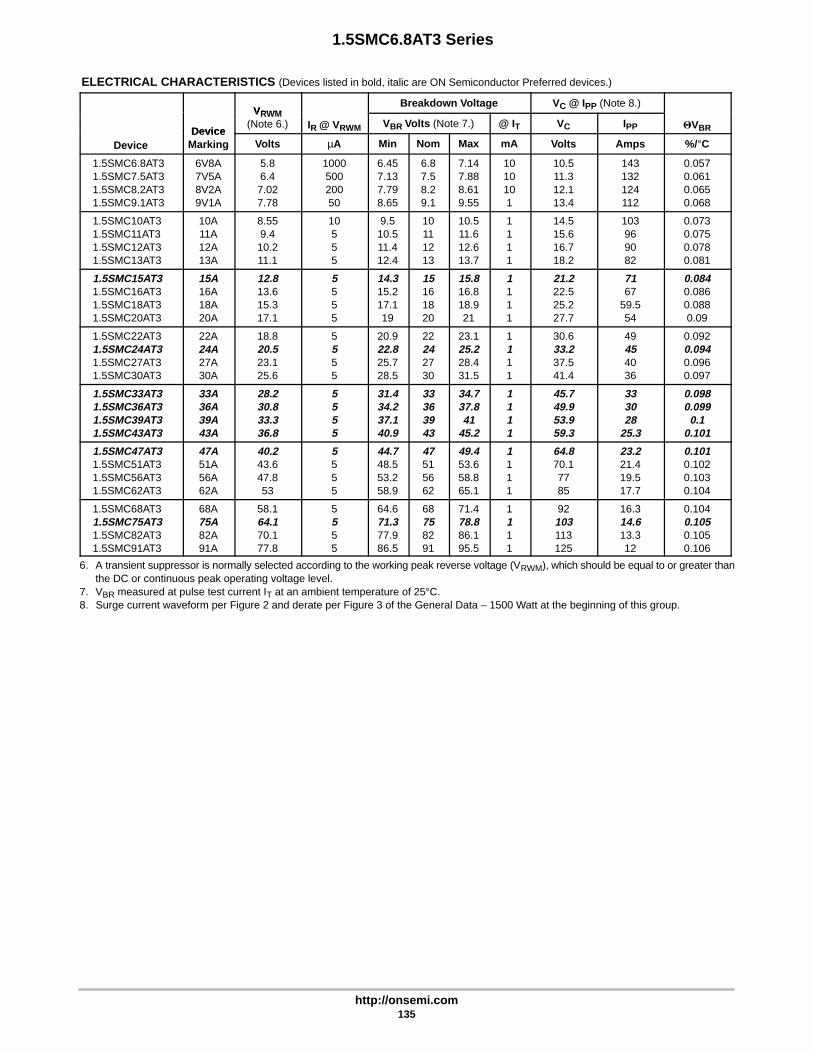
1.5SMC6.8AT3 Series
http://onsemi.com135
ELECTRICAL CHARACTERISTICS (Devices listed in bold, italic are ON Semiconductor Preferred devices.)
VRWMBreakdown Voltage VC @ IPP (Note 8.)
Device
VRWM(Note 6.) IR @ VRWM VBR Volts (Note 7.) @ IT VC IPP VBR
DeviceDevice
Marking Volts µA Min Nom Max mA Volts Amps %/°C
1.5SMC6.8AT31.5SMC7.5AT31.5SMC8.2AT31.5SMC9.1AT3
6V8A7V5A8V2A9V1A
5.86.47.027.78
100050020050
6.457.137.798.65
6.87.58.29.1
7.147.888.619.55
1010101
10.511.312.113.4
143132124112
0.0570.0610.0650.068
1.5SMC10AT31.5SMC11AT31.5SMC12AT31.5SMC13AT3
10A11A12A13A
8.559.410.211.1
10555
9.510.511.412.4
10111213
10.511.612.613.7
1111
14.515.616.718.2
103969082
0.0730.0750.0780.081
1.5SMC15AT31.5SMC16AT31.5SMC18AT31.5SMC20AT3
15A16A18A20A
12.813.615.317.1
5555
14.315.217.119
15161820
15.816.818.921
1111
21.222.525.227.7
7167
59.554
0.0840.0860.0880.09
1.5SMC22AT31.5SMC24AT31.5SMC27AT31.5SMC30AT3
22A24A27A30A
18.820.523.125.6
5555
20.922.825.728.5
22242730
23.125.228.431.5
1111
30.633.237.541.4
49454036
0.0920.0940.0960.097
1.5SMC33AT31.5SMC36AT31.5SMC39AT31.5SMC43AT3
33A36A39A43A
28.230.833.336.8
5555
31.434.237.140.9
33363943
34.737.841
45.2
1111
45.749.953.959.3
333028
25.3
0.0980.0990.1
0.101
1.5SMC47AT31.5SMC51AT31.5SMC56AT31.5SMC62AT3
47A51A56A62A
40.243.647.853
5555
44.748.553.258.9
47515662
49.453.658.865.1
1111
64.870.17785
23.221.419.517.7
0.1010.1020.1030.104
1.5SMC68AT31.5SMC75AT31.5SMC82AT31.5SMC91AT3
68A75A82A91A
58.164.170.177.8
5555
64.671.377.986.5
68758291
71.478.886.195.5
1111
92103113125
16.314.613.312
0.1040.1050.1050.106
6. A transient suppressor is normally selected according to the working peak reverse voltage (VRWM), which should be equal to or greater thanthe DC or continuous peak operating voltage level.
7. VBR measured at pulse test current IT at an ambient temperature of 25°C.8. Surge current waveform per Figure 2 and derate per Figure 3 of the General Data – 1500 Watt at the beginning of this group.

1.5SMC6.8AT3 Series
http://onsemi.com136
NONREPETITIVE
PULSE WAVEFORM
SHOWN IN FIGURE 2
tP, PULSE WIDTH
1
10
100
0.1 µs 1 µs 10 µs 100 µs 1 ms 10 ms
Figure 1. Pulse Rating Curve
0 1 2 3 40
50
100
t, TIME (ms)
VA
LUE
(%
)
HALF VALUE -IPP
2
PEAK VALUE - IPP
Figure 2. Pulse Waveform
Figure 3. Pulse Derating Curve
PE
AK
PU
LSE
DE
RAT
ING
IN %
OF
PE
AK
PO
WE
R O
R C
UR
RE
NT
@ T
A=
25C°
100
80
60
40
20
00 25 50 75 100 125 150
TA, AMBIENT TEMPERATURE (°C)
120
140
160
tP
PULSE WIDTH (tP) IS DEFINED
AS THAT POINT WHERE THE PEAK
CURRENT DECAYS TO 50%
OF IPP.
∆VBR, INSTANTANEOUS INCREASE IN VBR ABOVE VBR (NOM) (VOLTS)
0.3 0.5 0.7 1 2 3 5 7 10 20 30
1000
500
200
100
50
1
2
5
10
20
TL=25°CtP=10µs
VBR(NOM)=6.8TO13V
20V24V 43V
75V
120V
180V
Figure 4. Dynamic Impedance
Ppk
, PE
AK
PO
WE
R (
kW)
tr≤ 10 µs
I T, T
ES
T C
UR
RE
NT
(A
MP
S)
UL RECOGNITION
The entire series has Underwriters LaboratoryRecognition for the classification of protectors (QVGV2)under the UL standard for safety 497B and File #116110.Many competitors only have one or two devices recognizedor have recognition in a non-protective category. Somecompetitors have no recognition at all. With the UL497Brecognition, our parts successfully passed several tests
including Strike Voltage Breakdown test, EnduranceConditioning, Temperature test, Dielectric Voltage-Withstandtest, Discharge test and several more.
Whereas, some competitors have only passed aflammability test for the package material, we have beenrecognized for much more to be included in their Protectorcategory.

1.5SMC6.8AT3 Series
http://onsemi.com137
APPLICATION NOTES
RESPONSE TIMEIn most applications, the transient suppressor device is
placed in parallel with the equipment or component to beprotected. In this situation, there is a time delay associatedwith the capacitance of the device and an overshootcondition associated with the inductance of the device andthe inductance of the connection method. The capacitiveeffect is of minor importance in the parallel protectionscheme because it only produces a time delay in thetransition from the operating voltage to the clamp voltage asshown in Figure 5.
The inductive effects in the device are due to actualturn-on time (time required for the device to go from zerocurrent to full current) and lead inductance. This inductiveeffect produces an overshoot in the voltage across theequipment or component being protected as shown inFigure 6. Minimizing this overshoot is very important in theapplication, since the main purpose for adding a transientsuppressor is to clamp voltage spikes. The SMC series havea very good response time, typically < 1 ns and negligibleinductance. However, external inductive effects couldproduce unacceptable overshoot. Proper circuit layout,
minimum lead lengths and placing the suppressor device asclose as possible to the equipment or components to beprotected will minimize this overshoot.
Some input impedance represented by Zin is essential toprevent overstress of the protection device. This impedanceshould be as high as possible, without restricting the circuitoperation.
DUTY CYCLE DERATINGThe data of Figure 1 applies for non-repetitive conditions
and at a lead temperature of 25°C. If the duty cycle increases,the peak power must be reduced as indicated by the curvesof Figure 7. Average power must be derated as the lead orambient temperature rises above 25°C. The average powerderating curve normally given on data sheets may benormalized and used for this purpose.
At first glance the derating curves of Figure 7 appear to bein error as the 10 ms pulse has a higher derating factor thanthe 10 µs pulse. However, when the derating factor for agiven pulse of Figure 7 is multiplied by the peak power valueof Figure 1 for the same pulse, the results follow theexpected trend.
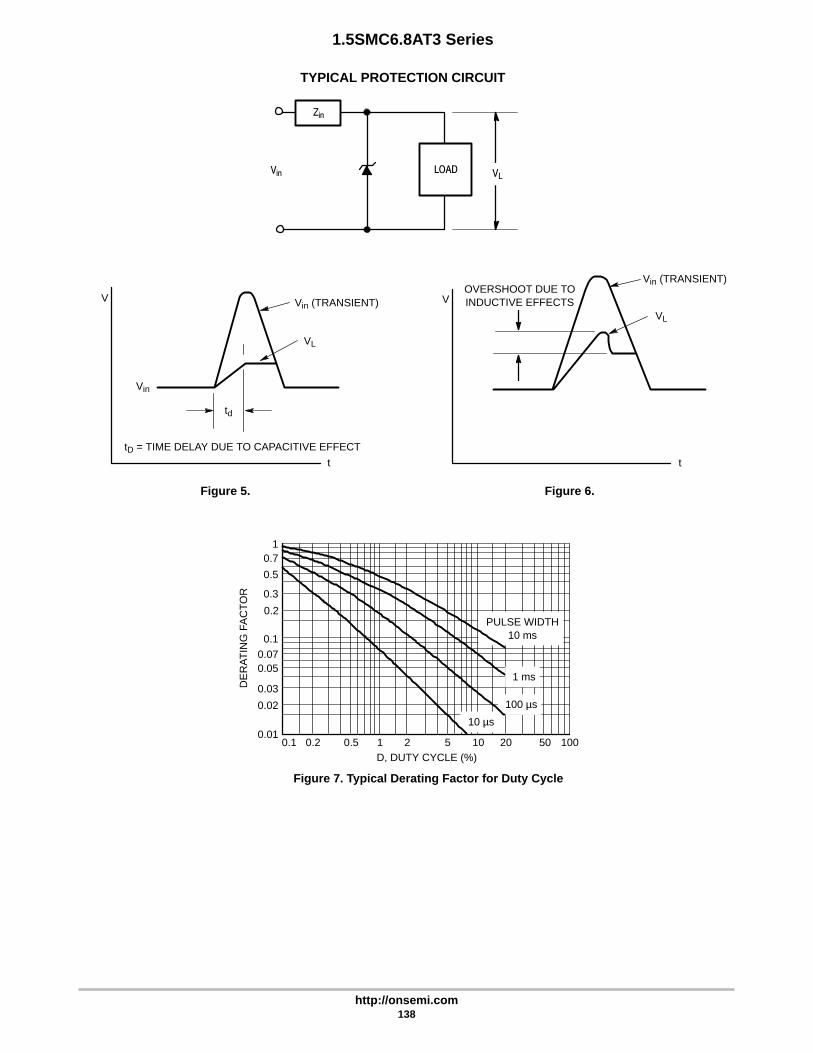
1.5SMC6.8AT3 Series
http://onsemi.com138
VL
V
Vin
Vin (TRANSIENT)VL
td
V
Vin (TRANSIENT)OVERSHOOT DUE TOINDUCTIVE EFFECTS
tD = TIME DELAY DUE TO CAPACITIVE EFFECT
t t
Figure 5. Figure 6.
Figure 7. Typical Derating Factor for Duty Cycle
DE
RA
TIN
G F
AC
TO
R
1 ms
10 µs
10.7
0.5
0.3
0.05
0.1
0.2
0.01
0.02
0.03
0.07
100 µs
0.1 0.2 0.5 2 5 10 501 20 100D, DUTY CYCLE (%)
PULSE WIDTH10 ms
TYPICAL PROTECTION CIRCUIT
Vin VL
Zin
LOAD

http://onsemi.com139
CHAPTER 5Transient Voltage Suppressor Arrays –
Surface Mounted Data Sheets
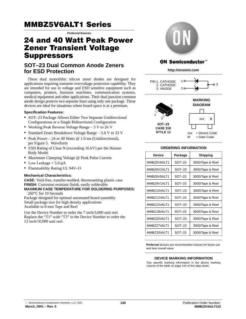
Semiconductor Components Industries, LLC, 2001
March, 2001 – Rev. 5140 Publication Order Number:
MMBZ5V6ALT1/D
MMBZ5V6ALT1 SeriesPreferred Devices
24 and 40 Watt Peak PowerZener Transient VoltageSuppressors
SOT–23 Dual Common Anode Zenersfor ESD Protection
These dual monolithic silicon zener diodes are designed forapplications requiring transient overvoltage protection capability. Theyare intended for use in voltage and ESD sensitive equipment such ascomputers, printers, business machines, communication systems,medical equipment and other applications. Their dual junction commonanode design protects two separate lines using only one package. Thesedevices are ideal for situations where board space is at a premium.
Specification Features:• SOT–23 Package Allows Either Two Separate Unidirectional
Configurations or a Single Bidirectional Configuration• Working Peak Reverse Voltage Range – 3 V to 26 V
• Standard Zener Breakdown Voltage Range – 5.6 V to 33 V
• Peak Power – 24 or 40 Watts @ 1.0 ms (Unidirectional),per Figure 5. Waveform
• ESD Rating of Class N (exceeding 16 kV) per the Human Body Model
• Maximum Clamping Voltage @ Peak Pulse Current• Low Leakage < 5.0 µA• Flammability Rating UL 94V–O
Mechanical Characteristics:CASE: Void-free, transfer-molded, thermosetting plastic caseFINISH: Corrosion resistant finish, easily solderableMAXIMUM CASE TEMPERATURE FOR SOLDERING PURPOSES:
260°C for 10 SecondsPackage designed for optimal automated board assemblySmall package size for high density applicationsAvailable in 8 mm Tape and Reel
Use the Device Number to order the 7 inch/3,000 unit reel.Replace the “T1” with “T3” in the Device Number to order the13 inch/10,000 unit reel.
Preferred devices are recommended choices for future useand best overall value.
SOT–23CASE 318STYLE 12
http://onsemi.com
13
2
12
3
PIN 1. CATHODE2. CATHODE3. ANODE
Device Package Shipping
ORDERING INFORMATION
MMBZ5V6ALT1 SOT–23 3000/Tape & Reel
MMBZ6V2ALT1 SOT–23 3000/Tape & Reel
MMBZ6V8ALT1 SOT–23 3000/Tape & Reel
MMBZ10VALT1 SOT–23 3000/Tape & Reel
xxx
MMBZ12VALT1 SOT–23 3000/Tape & Reel
MMBZ15VALT1 SOT–23 3000/Tape & Reel
MMBZ18VALT1 SOT–23 3000/Tape & Reel
MMBZ20VALT1 SOT–23 3000/Tape & Reel
MMBZ27VALT1 SOT–23 3000/Tape & Reel
MMBZ33VALT1 SOT–23 3000/Tape & Reel
MARKINGDIAGRAM
xxx = Device CodeM = Date Code
M
See specific marking information in the device markingcolumn of the table on page 142 of this data sheet.
DEVICE MARKING INFORMATION
MMBZ9V1ALT1 SOT–23 3000/Tape & Reel

Uni–Directional TVS
IPP
IF
V
I
IRIT
VRWMVC VBRVF
MMBZ5V6ALT1 Series
http://onsemi.com141
MAXIMUM RATINGS
Rating Symbol Value Unit
Peak Power Dissipation @ 1.0 ms (Note 1.) MMBZ5V6ALT1 thru MMBZ10VALT1@ TL ≤ 25°C MMBZ12VALT1 thru MMBZ33VALT1
Ppk 2440
Watts
Total Power Dissipation on FR–5 Board (Note 2.) @ TA = 25°CDerate above 25°C
°PD° 2251.8
°mW°mW/°C
Thermal Resistance Junction to Ambient RθJA 556 °C/W
Total Power Dissipation on Alumina Substrate (Note 3.) @ TA = 25°CDerate above 25°C
°PD° 3002.4
°mWmW/°C
Thermal Resistance Junction to Ambient RθJA 417 °C/W
Junction and Storage Temperature Range TJ, Tstg – 55 to +150 °C
Lead Solder Temperature – Maximum (10 Second Duration) TL 260 °C
1. Non–repetitive current pulse per Figure 5. and derate above TA = 25°C per Figure 6. 2. FR–5 = 1.0 x 0.75 x 0.62 in.3. Alumina = 0.4 x 0.3 x 0.024 in., 99.5% alumina
*Other voltages may be available upon request
ELECTRICAL CHARACTERISTICS(TA = 25°C unless otherwise noted)UNIDIRECTIONAL (Circuit tied to Pins 1 and 3 or 2 and 3)
Symbol Parameter
IPP Maximum Reverse Peak Pulse Current
VC Clamping Voltage @ IPP
VRWM Working Peak Reverse Voltage
IR Maximum Reverse Leakage Current @ VRWM
VBR Breakdown Voltage @ IT
IT Test Current
VBR Maximum Temperature Coefficient of VBR
IF Forward Current
VF Forward Voltage @ IF
ZZT Maximum Zener Impedance @ IZT
IZK Reverse Current
ZZK Maximum Zener Impedance @ IZK

MMBZ5V6ALT1 Series
http://onsemi.com142
ELECTRICAL CHARACTERISTICS (TA = 25°C unless otherwise noted)UNIDIRECTIONAL (Circuit tied to Pins 1 and 3 or Pins 2 and 3)
(VF = 0.9 V Max @ IF = 10 mA) 24 WATTS
IR @Breakdown Voltage
Max ZenerImpedance (Note 5.)
VC @ IPP(Note 6.)
Device VRWM
IR @VRWM VBR (Note 4.) (V) @ IT ZZT @ IZT ZZK @ IZK VC IPP VBR
DeviceDevice
Marking Volts A Min Nom Max mA Ω Ω mA V A mV/C
MMBZ5V6ALT1 5A6 3.0 5.0 5.32 5.6 5.88 20 11 1600 0.25 8.0 3.0 1.26
MMBZ6V2ALT1 6A2 3.0 0.5 5.89 6.2 6.51 1.0 – – – 8.7 2.76 2.80
(VF = 1.1 V Max @ IF = 200 mA)
Breakdown Voltage VC @ IPP (Note 6.)
Device VRWM IR @ VRWM VBR (Note 4.) (V) @ IT VC IPP VBR
DeviceDevice
Marking Volts A Min Nom Max mA V A mV/C
MMBZ6V8ALT1 6A8 4.5 0.5 6.46 6.8 7.14 1.0 9.6 2.5 3.4
MMBZ9V1ALT1 9A1 6.0 0.3 8.65 9.1 9.56 1.0 14 1.7 7.5
MMBZ10VALT1 10A 6.5 0.3 9.50 10 10.5 1.0 14.2 1.7 7.5
(VF = 1.1 V Max @ IF = 200 mA) 40 WATTS
Breakdown Voltage VC @ IPP (Note 6.)
Device VRWM IR @ VRWM VBR (Note 4.) (V) @ IT VC IPP VBR
DeviceDevice
Marking Volts nA Min Nom Max mA V A mV/C
MMBZ12VALT1 12A 8.5 200 11.40 12 12.60 1.0 17 2.35 7.5
MMBZ15VALT1 15A 12 50 14.25 15 15.75 1.0 21 1.9 12.3
MMBZ18VALT1 18A 14.5 50 17.10 18 18.90 1.0 25 1.6 15.3
MMBZ20VALT1 20A 17 50 19.00 20 21.00 1.0 28 1.4 17.2
MMBZ27VALT1 27A 22 50 25.65 27 28.35 1.0 40 1.0 24.3
MMBZ33VALT1 33A 26 50 31.35 33 34.65 1.0 46 0.87 30.4
4. VBR measured at pulse test current IT at an ambient temperature of 25°C.5. ZZT and ZZK are measured by dividing the AC voltage drop across the device by the AC current applied. The specified limits are for IZ(AC)
= 0.1 IZ(DC), with the AC frequency = 1.0 kHz.6. Surge current waveform per Figure 5. and derate per Figure 6.

MMBZ5V6ALT1 Series
http://onsemi.com143
TYPICAL CHARACTERISTICS
-40 +50
18
BR
EA
KD
OW
N V
OLT
AG
E (
VO
LTS
)
Figure 1. Typical Breakdown Voltageversus Temperature
(Upper curve for each voltage is bidirectional mode,lower curve is unidirectional mode)
0
TEMPERATURE (°C)
+100 +150
15
12
9
6
3
0
(VB
R@
IT
)
-40 +25
1000
Figure 2. Typical Leakage Currentversus Temperature
TEMPERATURE (°C)
+85 +125
100
10
1
0.1
0.01
I R(n
A)
Figure 3. Typical Capacitance versus Bias Voltage(Upper curve for each voltage is unidirectional mode,
lower curve is bidirectional mode)
0 25 50 75 100 125 150 175
300
250
200
150
100
50
0
Figure 4. Steady State Power Derating Curve
P D, P
OW
ER
DIS
SIP
AT
ION
(m
W)
TEMPERATURE (°C)
FR-5 BOARD
ALUMINA SUBSTRATE
0 1 2 3
320
280
240
160
120
40
0
C, C
APA
CIT
AN
CE
(pF
)
BIAS (V)
200
8015 V
5.6 V
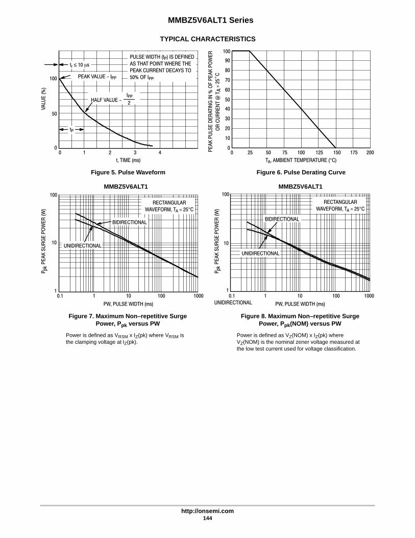
MMBZ5V6ALT1 Series
http://onsemi.com144
TYPICAL CHARACTERISTICSP
0.1 1 10 100 10001
10
100
Power is defined as VRSM x IZ(pk) where VRSM isthe clamping voltage at IZ(pk).
PW, PULSE WIDTH (ms)
UNIDIRECTIONAL
RECTANGULAR
WAVEFORM, TA = 25°C
BIDIRECTIONAL
pkP
EA
K S
UR
GE
PO
WE
R (
W)
MMBZ5V6ALT1
Figure 5. Pulse Waveform
VA
LUE
(%
)
100
50
00 1 2 3 4
t, TIME (ms)
Figure 6. Pulse Derating Curve
PULSE WIDTH (tP) IS DEFINED
AS THAT POINT WHERE THE
PEAK CURRENT DECAYS TO
50% OF IPP.
HALF VALUE-IPP
2
tP
tr ≤ 10 s
PEAK VALUE-IPP
100
90
80
70
60
50
40
30
20
10
00 25 50 75 100 125 150 175 200
TA, AMBIENT TEMPERATURE (°C)
Figure 7. Maximum Non–repetitive SurgePower, P pk versus PW
PE
AK
PU
LSE
DE
RAT
ING
IN %
OF
PE
AK
PO
WE
R
OR
CU
RR
EN
T @
TA
= 25
C°
Figure 8. Maximum Non–repetitive SurgePower, P pk(NOM) versus PW
0.1 1 10 100 10001
10
100
PW, PULSE WIDTH (ms)
P pk
PE
AK
SU
RG
E P
OW
ER
(W
)
UNIDIRECTIONAL
RECTANGULAR
WAVEFORM, TA = 25°C
BIDIRECTIONAL
MMBZ5V6ALT1
Power is defined as VZ(NOM) x IZ(pk) whereVZ(NOM) is the nominal zener voltage measured atthe low test current used for voltage classification.
UNIDIRECTIONAL

MMBZ5V6ALT1 Series
http://onsemi.com145
TYPICAL COMMON ANODE APPLICATIONS
A quad junction common anode design in a SOT–23package protects four separate lines using only one package.This adds flexibility and creativity to PCB design especially
when board space is at a premium. Two simplified examplesof TVS applications are illustrated below.
MMBZ5V6ALT1
THRU
MMBZ33VALT1
KEYBOARD
TERMINAL
PRINTER
ETC.
FUNCTIONAL
DECODERI/O
A
MMBZ5V6ALT1
THRU
MMBZ33VALT1
GND
Computer Interface Protection
B
C
D
Microprocessor Protection
I/O
RAM ROM
CLOCK
CPU
CONTROL BUS
ADDRESS BUS
DATA BUS
GND
VGG
VDD
MMBZ5V6ALT1
THRU
MMBZ33VALT1
SOLDERING PRECAUTIONS

Semiconductor Components Industries, LLC, 2001
April, 2001 – Rev. 5146 Publication Order Number:
MMBZ15VDLT1/D
MMBZ15VDLT1,MMBZ27VCLT1
Preferred Devices
40 Watt Peak PowerZener Transient VoltageSuppressors
SOT–23 Dual Common Cathode Zenersfor ESD Protection
These dual monolithic silicon zener diodes are designed forapplications requiring transient overvoltage protection capability. Theyare intended for use in voltage and ESD sensitive equipment such ascomputers, printers, business machines, communication systems,medical equipment and other applications. Their dual junction commoncathode design protects two separate lines using only one package.These devices are ideal for situations where board space is at apremium.
Specification Features:• SOT–23 Package Allows Either Two Separate Unidirectional
Configurations or a Single Bidirectional Configuration• Working Peak Reverse Voltage Range – 12.8 V, 22 V
• Standard Zener Breakdown Voltage Range – 15 V, 27 V
• Peak Power – 40 Watts @ 1.0 ms (Bidirectional),per Figure 5. Waveform
• ESD Rating of Class N (exceeding 16 kV) per the Human Body Model
• Maximum Clamping Voltage @ Peak Pulse Current• Low Leakage < 100 nA• Flammability Rating UL 94V–O
Mechanical Characteristics:CASE: Void-free, transfer-molded, thermosetting plastic caseFINISH: Corrosion resistant finish, easily solderableMAXIMUM CASE TEMPERATURE FOR SOLDERING PURPOSES:
260°C for 10 SecondsPackage designed for optimal automated board assemblySmall package size for high density applicationsAvailable in 8 mm Tape and Reel
Use the Device Number to order the 7 inch/3,000 unit reel.Replace the “T1” with “T3” in the Device Number to order the13 inch/10,000 unit reel.
Preferred devices are recommended choices for future useand best overall value.
SOT–23CASE 318STYLE 9
http://onsemi.com
13
2
12
3
PIN 1. ANODE2. ANODE3. CATHODE
Device Package Shipping
ORDERING INFORMATION
MMBZ15VDLT1 SOT–23 3000/Tape & Reel
MMBZ15VDLT3 SOT–23 10,000/Tape & Reel
MMBZ27VCLT1 SOT–23 3000/Tape & Reel
xxx
MARKING DIAGRAM
xxx = 15D or 27CM = Date Code
M

Uni–Directional TVS
IPP
IF
V
I
IRIT
VRWMVC VBRVF
MMBZ15VDLT1, MMBZ27VCLT1
http://onsemi.com147
MAXIMUM RATINGS
Rating Symbol Value Unit
Peak Power Dissipation @ 1.0 ms (Note 1.) @ TL ≤ 25°C Ppk 40 Watts
Total Power Dissipation on FR–5 Board (Note 2.) @ TA = 25°CDerate above 25°C
°PD° 2251.8
°mW°mW/°C
Thermal Resistance Junction to Ambient RθJA 556 °C/W
Total Power Dissipation on Alumina Substrate (Note 3.) @ TA = 25°CDerate above 25°C
°PD° 3002.4
°mWmW/°C
Thermal Resistance Junction to Ambient RθJA 417 °C/W
Junction and Storage Temperature Range TJ, Tstg – 55 to +150 °C
Lead Solder Temperature – Maximum (10 Second Duration) TL 230 °C
1. Non–repetitive current pulse per Figure 5. and derate above TA = 25°C per Figure 6. 2. FR–5 = 1.0 x 0.75 x 0.62 in.3. Alumina = 0.4 x 0.3 x 0.024 in., 99.5% alumina
ELECTRICAL CHARACTERISTICS(TA = 25°C unless otherwise noted)UNIDIRECTIONAL (Circuit tied to Pins 1 and 3 or 2 and 3)
Symbol Parameter
IPP Maximum Reverse Peak Pulse Current
VC Clamping Voltage @ IPP
VRWM Working Peak Reverse Voltage
IR Maximum Reverse Leakage Current @ VRWM
VBR Breakdown Voltage @ IT
IT Test Current
VBR Maximum Temperature Coefficient of VBR
IF Forward Current
VF Forward Voltage @ IF

MMBZ15VDLT1, MMBZ27VCLT1
http://onsemi.com148
ELECTRICAL CHARACTERISTICS (TA = 25°C unless otherwise noted)UNIDIRECTIONAL (Circuit tied to Pins 1 and 3 or Pins 2 and 3)
(VF = 0.9 V Max @ IF = 10 mA)
Breakdown Voltage VC @ IPP (Note 5.)
Device VRWM IR @ VRWM VBR (Note 4.) (V) @ IT VC IPP VBR
DeviceDevice
Marking Volts nA Min Nom Max mA V A mV/C
MMBZ15VDLT1 15D 12.8 100 14.3 15 15.8 1.0 21.2 1.9 12
(VF = 1.1 V Max @ IF = 200 mA)
Breakdown Voltage VC @ IPP (Note 5.)
Device VRWM IR @ VRWM VBR (Note 4.) (V) @ IT VC IPP VBR
DeviceDevice
Marking Volts nA Min Nom Max mA V A mV/C
MMBZ27VCLT1 27C 22 50 25.65 27 28.35 1.0 38 1.0 26
4. VBR measured at pulse test current IT at an ambient temperature of 25°C.5. Surge current waveform per Figure 5. and derate per Figure 6.
-40 +85
17
BR
EA
KD
OW
N V
OLT
AG
E (
VO
LTS
)
Figure 1. Typical Breakdown Voltageversus Temperature
TEMPERATURE (°C)
+125
16
15
14
13
(VB
R@
IT
)
+25
MMBZ15VDLT1
-55 +85
29B
RE
AK
DO
WN
VO
LTA
GE
(V
OLT
S)
Figure 2. Typical Breakdown Voltageversus Temperature
TEMPERATURE (°C)
+125
28
27
26
25
(VB
R@
IT
)
+25
MMBZ27VCLT1
TYPICAL CHARACTERISTICS
BIDIRECTIONAL
UNIDIRECTIONAL
BIDIRECTIONAL

MMBZ15VDLT1, MMBZ27VCLT1
http://onsemi.com149
10000
10
0.01
TEMPERATURE (°C)
I R(n
A)
Figure 3. Typical Leakage Currentversus Temperature
100
1
0.1
-40 +85 +125+25
0 25 50 75 100 125 150 175
300
250
200
150
100
50
0
Figure 4. Steady State Power Derating Curve
P D, P
OW
ER
DIS
SIP
AT
ION
(m
W)
TEMPERATURE (°C)
FR-5 BOARD
ALUMINA SUBSTRATEV
ALU
E (
%)
100
50
00 1 2 3 4
t, TIME (ms)
Figure 5. Pulse Waveform
tr ≤ 10 s
PULSE WIDTH (tP) IS DEFINED
AS THAT POINT WHERE THE
PEAK CURRENT DECAYS TO
50% OF IPP.
HALF VALUEIPP
2
PEAK VALUEIPP
tP
100
90
80
70
60
50
40
30
20
10
00 25 50 75 100 125 150 175 200
TA, AMBIENT TEMPERATURE (°C)
Figure 6. Pulse Derating Curve
PE
AK
PU
LSE
DE
RAT
ING
IN %
OF
PE
AK
PO
WE
R
OR
CU
RR
EN
T @
TA
= 25
C°
SOLDERING PRECAUTIONS

Semiconductor Components Industries, LLC, 2001
March, 2001 – Rev. 4150 Publication Order Number:
MMQA5V6T1/D
MMQA5V6T1 Series
24 Watt Peak Power ZenerTransient Voltage Suppressors
SC–59 Quad Common Anode for ZenersESD Protection
These quad monolithic silicon voltage suppressors are designed forapplications requiring transient voltage protection capability. They areintended for use in voltage and ESD sensitive equipment such ascomputers, printers, business machines, communication systems, medicalequipment, and other applications. Their quad junction common anodedesign protects four separate lines using only one package. These devicesare ideal for situations where board space is at a premium.
Specification Features:• SC–59 Package Allows Four Separate Unidirectional Configurations
• Working Peak Reverse Voltage Range – 3.0 V to 2.5 V
• Standard Zener Breakdown Voltage Range – 5.6 V to 33 V
• Peak Power – Minimum 24 W @ 1 ms (Unidirectional), per Figure 5
• Peak Power – Minimum 150 W @ 20 s (Unidirectional), per Figure 6
• ESD Rating of Class 3 (> 16 KV) per Human Body Model
• Maximum Clamp Voltage @ Peak Pulse Current
• Package Designed for Optimal Automated Board Assembly
• Small Package Size for High Density Applications
• Low Leakage < 2.0 A
Mechanical Characteristics:CASE: Void-free, transfer-molded, thermosetting plasticFINISH: All external surfaces are corrosion resistant and leads are
readily solderableMAXIMUM CASE TEMPERATURE FOR SOLDERING PURPOSES:
260°C for 10 Seconds
MAXIMUM RATINGS
Rating Symbol Value Unit
Peak Power Dissipation (Note 1.)@ 1.0 ms @ TL ≤ 25°C
PPK 24 W
Peak Power Dissipation (Note 2.)@ 20 s @ TL ≤ 25°C
PPK 150 W
Total Power Dissipation (Note 3.) @ TA = 25°CDerate Above 25°C
Thermal Resistance – Junction to Ambient
PD
RJA
2251.8556
mWmW/°C°C/W
Total Power Dissipation (Note 4.) @ TA = 25°CDerate Above 25°C
Thermal Resistance – Junction to Ambient
PD
RJA
3002.4417
mWmW/°C°C/W
Junction and Storage Temperature Range TJ, Tstg –55 to+150
°C
1. Nonrepetitive current pulse per Figure 5 and derated above TA = 25°C perFigure 4
2. Nonrepetitive current pulse per Figure 6 and derated above TA = 25°C perFigure 4
3. FR–5 board = 1.0 X 0.75 X 0.62 in.4. Alumina substrate = 0.4 X 0.3 X 0.024 in., 99.5% alumina
Device Package Shipping
ORDERING INFORMATION
MMQAxxxT1 SC–59 3000/Tape & Reel
http://onsemi.com
†The “T1” suffix refers to an 8 mm, 7 inch reel.The “T3” suffix refers to an 8 mm, 13 inch reel.
MMQAxxxT3 SC–59 10,000/Tape & Reel
12
3
45
6
PIN 1. CATHODE2. ANODE3. CATHODE4. CATHODE5. ANODE6. CATHODE
1
2
3
6
5
4
xxx = Device Code= (See Table Next Page)
M = Date Code
MARKING DIAGRAM
xxx
PIN ASSIGNMENT
M
SC–59CASE 318F
STYLE 1

Uni–Directional TVS
IPP
IF
V
I
IRIT
VRWMVC VBRVF
MMQA5V6T1 Series
http://onsemi.com151
ELECTRICAL CHARACTERISTICS (TA = 25°C unlessotherwise noted, VF = 0.9 V Max. @ IF (Note 5.) = 10 mA)
Unidirectional (Circuit tied to Pins 1, 2 and 5; Pins 2, 3 and5; or 2, 4 and 6; or Pins 2, 5 and 6)
Symbol Parameter
IPP Maximum Reverse Peak Pulse Current
VC Clamping Voltage @ IPP
VRWM Working Peak Reverse Voltage
IR Maximum Reverse Leakage Current @ VRWM
ZZT Maximum Zener Impedance @ IZT
VBR Breakdown Voltage @ IT
IT Test Current
VBR Maximum Temperature Coefficient of VBR
IF Forward Current
VF Forward Voltage @ IF
ELECTRICAL CHARACTERISTICS
IR @Breakdown Voltage
ZZT (Note 6 )VC @ IPP (Note 7.)
DeviceVRWM
IR @VRWM VBR (Note 5.) (Volts) @ IT
ZZT (Note 6.)@ IZT VC IPP VBR
DeviceDevice
Marking Volts nA Min Nom Max mA mA Volts Amps mW/C
MMQA5V6T1 5A6 3.0 2000 5.32 5.6 5.88 1.0 400 1.0 8.0 3.0 1.26MMQA6V2T1 6A2 4.0 700 5.89 6.2 6.51 1.0 300 1.0 9.0 2.66 10.6MMQA6V8T1 6A8 4.3 500 6.46 6.8 7.14 1.0 300 1.0 9.8 2.45 10.9MMQA12VT1 12A 9.1 75 11.4 12 12.6 1.0 80 1.0 17.3 1.39 14
MMQA13VT1 13A 9.8 75 12.35 13 13.65 1.0 80 1.0 18.6 1.29 15MMQA15VT1 15A 11 75 14.25 15 15.75 1.0 80 1.0 21.7 1.1 16MMQA18VT1 18A 14 75 17.1 18 18.9 1.0 80 1.0 26 0.923 19MMQA20VT1 20A 15 75 19.0 20 21.0 1.0 80 1.0 28.6 0.84 20.1
MMQA21VT1 21A 16 75 19.95 21 22.05 1.0 80 1.0 30.3 0.792 21MMQA22VT1 22A 17 75 20.9 22 23.1 1.0 80 1.0 31.7 0.758 22MMQA24VT1 24A 18 75 22.8 24 25.2 1.0 100 1.0 34.6 0.694 25MMQA27VT1 27A 21 75 25.65 27 28.35 1.0 125 1.0 39.0 0.615 28
MMQA30VT1 30A 23 75 28.5 30 31.5 1.0 150 1.0 43.3 0.554 32MMQA33VT1 33A 25 75 31.35 33 34.65 1.0 200 1.0 48.6 0.504 37
5. VBR measured at pulse test current IT at an ambient temperature of 25°C6. ZZT is measured by dividing the AC voltage drop across the device by the AC current supplied. The specified limits are IZ(ac) = 0.1 IZ(dc)
with the AC frequency = 1.0 kHz7. Surge current waveform per Figure 5 and derate per Figure 4

MMQA5V6T1 Series
http://onsemi.com152
TYPICAL CHARACTERISTICS
300
VZ, NOMINAL ZENER VOLTAGE (V)
C, C
APA
CIT
AN
CE
(pF
)
250
200
150
100
50
05.6 6.8 12 20 27
BIASED AT 0 V
BIASED AT 1 V
BIASED AT 50%
OF VZ NOM
Figure 1. Typical Capacitance
5.6 6.8 20 27
10,000
1,000
100
10
0
Figure 2. Typical Leakage Current
I R, L
EA
KA
GE
(nA
)
VZ, NOMINAL ZENER VOLTAGE (V)
33 33
+150°C
+25°C
-40°C
Figure 3. Steady State Power Derating Curve Figure 4. Pulse Derating Curve
0 25 50 75 100 125 150 175
300
250
200
150
100
50
0
P D, P
OW
ER
DIS
SIP
AT
ION
(m
W)
TA, AMBIENT TEMPERATURE (°C)
FR5 BOARD
ALUMINA SUBSTRATE
100
90
80
70
60
50
40
30
20
10
00 25 50 75 100 125 150 175 200
TA, AMBIENT TEMPERATURE (°C)
PE
AK
PU
LSE
DE
RAT
ING
IN %
OF
PE
AK
PO
WE
R
OR
CU
RR
EN
T @
TA
= 25
C°

MMQA5V6T1 Series
http://onsemi.com153
TYPICAL CHARACTERISTICS
Figure 5. 10 × 1000 s Pulse Waveform
VA
LUE
(%
)
100
50
00 1 2 3 4
t, TIME (ms)
tr
tP
PULSE WIDTH (tP) IS DEFINED
AS THAT POINT WHERE THE
PEAK CURRENT DECAYS TO 50%
OF IRSM.
tr ≤ 10 µs
HALF VALUEIRSM
2
PEAK VALUEIRSM
Figure 6. 8 × 20 s Pulse Waveform
Figure 7. Maximum Non–Repetitive SurgePower, Ppk versus PW
Figure 8. Typical Maximum Non–RepetitiveSurge Power, Ppk versus V BR
Ppk
PE
AK
SU
RG
E P
OW
ER
(W
)
0.1 1.0 10 100 10001.0
10
100
Power is defined as VRSM x IZ(pk) where VRSMis the clamping voltage at IZ(pk).
PW, PULSE WIDTH (ms)
UNIDIRECTIONAL
RECTANGULAR
WAVEFORM, TA = 25°C
100
90
80
70
60
50
40
30
20
10
00 20 40 60 80
t, TIME (s)
% O
F P
EA
K P
ULS
E C
UR
RE
NT
200
180
160
140
120
100
80
60
40
20
05.6 6.8 12 20 33
NOMINAL VZ
P
tP
tr
PULSE WIDTH (tP) IS DEFINED
AS THAT POINT WHERE THE
PEAK CURRENT DECAY = 8 s
PEAK VALUE IRSM @ 8 s
HALF VALUE IRSM/2 @ 20 s
27
, PE
AK
SU
RG
E P
OW
ER
(W
)P
K
8 × 20 WAVEFORM AS PER FIGURE 6
10 × 100 WAVEFORM AS PER FIGURE 5

MMQA5V6T1 Series
http://onsemi.com154
TYPICAL COMMON ANODE APPLICATIONS
A quad junction common anode design in a SC-74package protects four separate lines using only one package.This adds flexibility and creativity to PCB design especially
when board space is at a premium. A simplified example ofMMQA Series Device applications is illustrated below.
KEYBOARD
TERMINAL
PRINTER
ETC.
FUNCTIONAL
DECODERI/O
A
MMQA SERIES DEVICE
GND
Computer Interface Protection
B
C
D
Microprocessor Protection
I/O
RAM ROM
CLOCK
CPU
CONTROL BUS
ADDRESS BUS
DATA BUS
GND
VGG
VDD
MMQA SERIES DEVICE

Semiconductor Components Industries, LLC, 2001
March, 2001 – Rev. 1155 Publication Order Number:
MSQA6V1W5T2/D
MSQA6V1W5T2
Quad Array forESD Protection
This quad monolithic silicon voltage suppressor is designed forapplications requiring transient overvoltage protection capability. It isintended for use in voltage and ESD sensitive equipment such ascomputers, printers, business machines, communication systems,medical equipment, and other applications. Its quad junction commonanode design protects four separate lines using only one package.These devices are ideal for situations where board space is at apremium.
Specification Features• SC88A Package Allows Four Separate Unidirectional Configurations
• Low Leakage < 1 A @ 3 Volt
• Breakdown Voltage: 6.1 Volt – 7.2 Volt @ 1 mA
• Low Capacitance (90 pF typical)
• ESD Protection Meeting IEC1000–4–2
Mechanical Characteristics• Void Free, Transfer–Molded, Thermosetting Plastic Case
• Corrosion Resistant Finish, Easily Solderable
• Package Designed for Optimal Automated Board Assembly
• Small Package Size for High Density Applications
SC–88A/SOT–323CASE 419A
http://onsemi.com
5
4
1
2
3
Device Package Shipping
ORDERING INFORMATION
MSQA6V1W5T2 SC–88A 3000/Tape & Reel
61 = Device MarkingD = One Digit Date Code
61 D
MARKINGDIAGRAM
1 32
4 5
NOTE: T2 Suffix Devices are Packaged with Pin 1NOTE: Opposing Sprocket Hole.

MSQA6V1W5T2
http://onsemi.com156
MAXIMUM RATINGS (TA = 25°C unless otherwise noted)
Characteristic Symbol Value Unit
Peak Power Dissipation @ 20 s @TA ≤ 25°C (Note 1.) Ppk 150 Watts
Steady State Power – 1 Diode (Note 2.) PD 385 mW
Thermal Resistance Junction to AmbientAbove 25°C, Derate
RJA 3253.1
°C/WmW/°C
Maximum Junction Temperature TJmax 150 °C
Operating Junction and Storage Temperature Range TJ Tstg –55 to +150 °C
ESD Discharge MIL STD 883C – Method 3015–6IEC1000–4–2, Air DischargeIEC1000–4–2, Contact Discharge
VPP 16169
kV
Lead Solder Temperature (10 seconds duration) TL 260 °C
ELECTRICAL CHARACTERISTICS
Breakdown VoltageVBR @ 1 mA (Volts)
Leakage CurrentIRM @ VRM = 3 V
Capacitance@ 0 V Bias
MaxVF @ IF = 200 mA
Device Min Nom Max (A) (pF) (V)
MSQA6V1W5 6.1 6.6 7.2 1.0 90 1.25
1. Non–repetitive current per Figure 1. Derate per Figure 2.2. Only 1 diode under power. For all 4 diodes under power, PD will be 25%. Mounted on FR–4 board with min pad.
Figure 1. Pulse Width Figure 2. 8 × 20 s Pulse Waveform
P
100
10
11 10 100 1000
t, TIME (s)
1000
, PE
AK
SU
RG
E P
OW
ER
(W
AT
TS
)pk NOTE: Non–Repetitive Surge.
100
90
80
70
60
50
40
30
20
10
00 20 40 60 80
t, TIME (s)
% O
F P
EA
K P
ULS
E C
UR
RE
NT
tP
tr
PULSE WIDTH (tP) IS DEFINED
AS THAT POINT WHERE THE
PEAK CURRENT DECAY = 8 s
PEAK VALUE IRSM @ 8 s
HALF VALUE IRSM/2 @ 20 s

MSQA6V1W5T2
http://onsemi.com157
Figure 3. Pulse Derating Curve Figure 4. Capacitance
Figure 5. Forward Voltage Figure 6. Clamping Voltage versus PeakPulse Current (Reverse Direction)
0.6 0.7 0.8 0.90.001
0.01
1.0
VF, FORWARD VOLTAGE (VOLTS)
100
90
80
70
60
50
40
30
20
10
00 1.0 3.0 5.0
BIAS VOLTAGE (VOLTS)
TY
PIC
AL
CA
PA
CIT
AN
CE
(pF
)
100
10
1.00 5.0 10 20 30
VC, CLAMPING VOLTAGE (VOLTS)
I
25
, PE
AK
PU
LSE
CU
RR
EN
T (A
MP
S)
pp
4.02.0
1 M
Hz
FR
EQ
UE
NC
Y
1.0 1.1 1.2
0.1
I, F
OR
WA
RD
CU
RR
EN
T (A
)F
15
2.5 s SQUARE WAVE
100
90
80
70
60
50
40
30
20
10
00 25 50 75 100 125 150 175 200
TA, AMBIENT TEMPERATURE (°C)
OR
CU
RR
EN
T @
TA
= 25
C°
Figure 7. Clamping Voltage versus PeakPulse Current (Forward Direction)
100
10
0.10 2.0 4.0 8.0 12
VC, FORWARD CLAMPING VOLTAGE (VOLTS)
I
10
, PE
AK
FO
RW
AR
D P
ULS
E C
UR
RE
NT
(AM
PS
)pp
6.0
2.5 s SQUARE WAVE
1.0

Semiconductor Components Industries, LLC, 2001
May, 2001 – Rev. 0158 Publication Order Number:
DF6A6.8FUT1/D
DF6A6.8FUT1
Quad Array forESD Protection
This quad voltage suppressor is designed for applications requiringtransient overvoltage protection capability. It is intended for use involtage and ESD sensitive equipment such as computers, printers,business machines, communication systems, medical equipment, andother applications. Its quad junction common anode design protectsfour separate lines using only one package. These devices are ideal forsituations where board space is at a premium.
Specification Features• SC–88 Package Allows Four Separate Unidirectional Configurations
• Low Leakage < 1 A @ 5 Volt
• Breakdown Voltage: 6.4 – 7.2 Volt @ 5 mA
• Low Capacitance (40 pF typical)
• ESD Protection Meeting 61000–4–2 Level 4and 16 kV Human Body Model
Mechanical Characteristics• Void Free, Transfer–Molded, Thermosetting Plastic Case
• Corrosion Resistant Finish, Easily Solderable
• Package Designed for Optimal Automated Board Assembly
• Small Package Size for High Density Applications
MAXIMUM RATINGS (TA = 25°C unless otherwise noted)
Rating Symbol Value Unit
Peak Power Dissipation @ 8 x 20 s(Note 1)
Ppk 75 Watts
Steady State Power Dissipation(Note 2)
PD 385 mW
Thermal Resistance –Junction to AmbientDerate Above 25°C
RJA3283.0
°C/WmW/°C
Maximum Junction Temperature TJmax 150 °C
Operating Junction and StorageTemperature Range
TJ, Tstg –55 to+150
°C
ESD DischargeMIL STD 883C – Method 3015–6IEC61000–4–2, Air DischargeIEC61000–4–2, Contact Discharge
VPP16168
kV
Lead Solder Temperature(10 seconds duration)
TL 260 °C
1. Per Waveform Figure 12. Mounted on FR–5 Board = 1.0 X 0.75 X 0.062 in.
SC–88CASE 419B
PLASTIC
http://onsemi.com
6
4
1
3
Device Package Shipping
ORDERING INFORMATION
DF6A6.8FUT1 SC–88 3000/Tape & Reel
68 = Device Markingd = One Digit Date Code
= Pin 1 Indicator
MARKINGDIAGRAM
1 32
6 4
68d
5
52

DF6A6.8FUT1
http://onsemi.com159
V–I Curve
IF
V
I
IRIT
VRWMVBRVF
ELECTRICAL CHARACTERISTICS
Device
Breakdown VoltageVBR @ 5 mA (Volts)
Leakage CurrentIRM @ VRWM = 5 V
TypicalCapacitance@ 0 V Bias
MaxVF @ IF = 10 mA
MaxZZ @5 mA
MaxZZK @0.5 mA
DeviceDevice
Marking Min Nom Max (A) (pF) (V) () ()
DF6A6.8FUT1 68 6.4 6.8 7.2 1.0 40 1.25 30 300
Figure 1. 8 × 20 s Pulse Waveform
100
90
80
70
60
50
40
30
20
10
00 20 40 60 80
t, TIME (s)
% O
F P
EA
K P
ULS
E C
UR
RE
NT
tP
tr
PULSE WIDTH (tP) IS DEFINED
AS THAT POINT WHERE THE
PEAK CURRENT DECAY = 8 s
PEAK VALUE IRSM @ 8 s
HALF VALUE IRSM/2 @ 20 s
Figure 2. Capacitance
45
40
35
30
50
25
15
20
100 1 3 5
BIAS VOLTAGE (VOLTS)
TY
PIC
AL
CA
PA
CIT
AN
CE
(pF
)
42
1 M
Hz
FR
EQ
UE
NC
Y
Figure 3. Forward Voltage Figure 4. Clamping Voltage versus PeakPulse Current
0.6 0.7 0.8 0.9
VF, FORWARD VOLTAGE (VOLTS)
10
18 9 10 12
VC, CLAMPING VOLTAGE (VOLTS)
I, P
EA
K P
ULS
E C
UR
RE
NT
(A
MP
S)
pp
1.0 1.1 1.2
I, F
OR
WA
RD
CU
RR
EN
T (
A)
F
11
8 x 20 s per Figure 1
0.0001
0.01
0.1
1
0.001
Semiconductor Components Industries, LLC, 2001
March, 2001 – Rev. 2160 Publication Order Number:
SMS05T1/D
SMS05T1
SC-74 Quad TransientVoltage Suppressor
for ESD ProtectionThis quad monolithic silicon voltage suppressor is designed for
applications requiring transient overvoltage protection capability. It isintended for use in voltage and ESD sensitive equipment such ascomputers, printers, business machines, communication systems andother applications. This quad device provides superior surgeprotection over current quad Zener MMQA series by providing up to350 watts peak power.
Features:• SC-74 Package Allows Four Separate Unidirectional Configurations• Peak Power – 350 Watts, 8 x 20 S• ESD Rating of Class N (Exceeding 25 kV) per the
Human Body Model• ESD Rating:
IEC 61000–4–2 (ESD) 15 kV (air) 8 kV (contact)IEC 61000–4–4 (EFT) 40 Amps (5/50 ns)IEC 61000–4–5 (lighting) 23 Amps (8/20 s)
• UL Flammability Rating of 94V–0
Typical Applications:• Hand Held Portable Applications such as Cell Phones, Pagers,
Notebooks and Notebook Computers
MAXIMUM RATINGS
Rating Symbol Value Unit
Peak Power Dissipation8 x 20 S @ TA = 25°C (Note 1.)
Ppk 350 W
Total Power Dissipation on FR–5 Board@ TA = 25°C (Note 2.)Derate Above 25°C
PD 225
1.8
mW
mW/°C
Thermal Resistance,Junction–to–Ambient
RJA 556 °C/W
Junction and StorageTemperature Range
TJ, Tstg –55 to+150
°C
Lead Solder Temperature –Maximum 10 Seconds Duration
TL 260 °C
1. Non–repetitive current pulse 8 x 20 S exponential decay waveform2. FR–5 = 1.0 x 0.75 x 0.62 in.
SC–74 QUAD TRANSIENTVOLTAGE SUPPRESSOR
350 WATTS PEAK POWER5 VOLTS
SC–74CASE 318F
STYLE 1
http://onsemi.com
12
3
45
6
1
2
3
6
5
4
xxx = Device Coded = Date Code
MARKING DIAGRAM
PIN ASSIGNMENT
Device Package Shipping
ORDERING INFORMATION
SMS05T1 SC–74 3000/Tape & Reel
SMS05T3 SC–74 10,000/Tape & Reel
xxx d
PIN 1. CATHODE2. ANODE3. CATHODE4. CATHODE5. ANODE6. CATHODE

SMS05T1
http://onsemi.com161
IPP
V
I
IRIT
VRWMVC VBR
ELECTRICAL CHARACTERISTICS
Characteristic Symbol Min Typ Max Unit
Reverse Breakdown Voltage @ It = 1.0 mA VBR 6.0 – 7.2 V
Reverse Leakage Current @ VRWN = 5.0 Volts IR N/A – 20 A
Maximum Clamping Voltage @ IPP = 5.0 A, 8 x 20 S VC N/A – 9.8 V
Maximum Clamping Voltage @ IPP = 23 A, 8 x 20 S VC N/A – 15.5 V
Between I/O Pins and Ground @ VR = 0 Volts, 1.0 MHz Capacitance 250 300 400 pF
Figure 1. Non–Repetitive Peak Pulse Powerversus Pulse Time
tp, PULSE DURATION (s)
10
1
0.1
10001001010.1
Figure 2. Power Derating Curve
TA, AMBIENT TEMPERATURE (°C)
1501251007550250
90
80
70
60
50
40
30
20
1000.01
100
110
PP
P, P
EA
K P
ULS
E P
OW
ER
(kW
)
% O
F R
AT
ED
PO
WE
R O
R I P
P
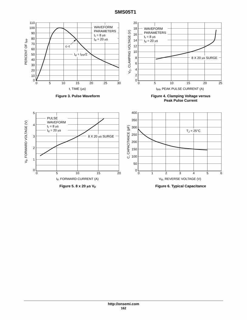
SMS05T1
http://onsemi.com162
Figure 3. Pulse Waveform
t, TIME (s)
30151050
Figure 4. Clamping Voltage versusPeak Pulse Current
IPP, PEAK PULSE CURRENT (A)
2520151050
12
10
8
6
4
2
0
14
20P
ER
CE
NT
OF
I PP
VC
, CLA
MP
ING
VO
LTA
GE
(V
)
Figure 5. 8 x 20 s VF
IF, FORWARD CURRENT (A)
5
3
1
1050
Figure 6. Typical Capacitance
VR, REVERSE VOLTAGE (V)
6543210
150
100
50
00
200
250
VF,
FO
RW
AR
D V
OLT
AG
E (
V)
C, C
AP
AC
ITA
NC
E (
pF)
2520
90
80
70
60
50
40
30
20
100
100
110WAVEFORMPARAMETERStr = 8 std = 20 s
td = IPP/2
4
2015
PULSEWAVEFORMtr = 8 std = 20 s
WAVEFORMPARAMETERStr = 8 std = 20 s
16
18
8 X 20 s SURGE
2
350
300
400
TJ = 25°C
c–t
8 X 20 s SURGE

http://onsemi.com163
CHAPTER 6Zener Voltage Regulator Diodes –
Axial Leaded Data Sheets

http://onsemi.com164

Semiconductor Components Industries, LLC, 2001
May, 2001 – Rev. 1165 Publication Order Number:
1N4370A/D
1N4370A Series
500 mW DO-35 HermeticallySealed Glass Zener VoltageRegulators
This is a complete series of 500 mW Zener diodes with limits andexcellent operating characteristics that reflect the superior capabilitiesof silicon–oxide passivated junctions. All this in an axial–leadhermetically sealed glass package that offers protection in all commonenvironmental conditions.
Specification Features:• Zener Voltage Range – 2.4 V to 12 V
• ESD Rating of Class 3 (>16 KV) per Human Body Model
• DO–204AH (DO–35) Package – Smaller than ConventionalDO–204AA Package
• Double Slug Type Construction
• Metallurgical Bonded Construction
Mechanical Characteristics:CASE: Double slug type, hermetically sealed glassFINISH: All external surfaces are corrosion resistant and leads arereadily solderableMAXIMUM LEAD TEMPERATURE FOR SOLDERING PURPOSES:230°C, 1/16″ from the case for 10 secondsPOLARITY: Cathode indicated by polarity bandMOUNTING POSITION: Any
MAXIMUM RATINGS (Note 1.)
Rating Symbol Value Unit
Max. Steady State Power Dissipation@ TL ≤ 75°C, Lead Length = 3/8″Derate above 75°C
PD 500
4.0
mW
mW/°C
Operating and StorageTemperature Range
TJ, Tstg –65 to+200
°C
1. Some part number series have lower JEDEC registered ratings.
Devices listed in bold, italic are ON SemiconductorPreferred devices. Preferred devices are recommendedchoices for future use and best overall value.
Device Package Shipping
ORDERING INFORMATION
1NxxxxA Axial Lead 3000 Units/Box
1NxxxxARL Axial Lead
AXIAL LEADCASE 299
GLASS
http://onsemi.com
5000/Tape & Reel
Cathode Anode
1NxxxxARL2 * Axial Lead 5000/Tape & Reel
1NxxxxARA1 Axial Lead 3000/Ammo Pack
1NxxxxATA Axial Lead 5000/Ammo Pack
* The “2” suffix refers to 26 mm tape spacing. Polarity band up with cathode lead off first Polarity band down with cathode lead off first
L1NxxxxAYWW
L = Assembly Location1NxxxxA = Device Code
= (See Table Next Page)Y = YearWW = Work Week
1NxxxxATA2 * Axial Lead 5000/Tape & Reel
1NxxxxARR1 Axial Lead 3000/Tape & Reel
1NxxxxARR2 Axial Lead 3000/Tape & Reel
MARKING DIAGRAM
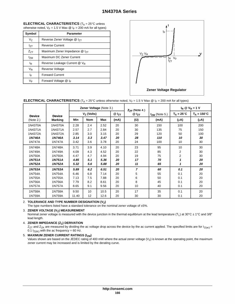
Zener Voltage Regulator
IF
V
I
IRIZT
VRVZ
VF
1N4370A Series
http://onsemi.com166
ELECTRICAL CHARACTERISTICS (TA = 25°C unlessotherwise noted, VF = 1.5 V Max @ IF = 200 mA for all types)
Symbol Parameter
VZ Reverse Zener Voltage @ IZT
IZT Reverse Current
ZZT Maximum Zener Impedance @ IZT
IZM Maximum DC Zener Current
IR Reverse Leakage Current @ VR
VR Reverse Voltage
IF Forward Current
VF Forward Voltage @ IF
ELECTRICAL CHARACTERISTICS (TA = 25°C unless otherwise noted, VF = 1.5 V Max @ IF = 200 mA for all types)
Zener Voltage (Note 3.)ZZT (Note 4 )
IR @ VR = 1 V
Device DeviceVZ (Volts) @ IZT
ZZT (Note 4.)@ IZT IZM (Note 5.) TA = 25C TA = 150C
Device(Note 2.)
DeviceMarking Min Nom Max (mA) () (mA) (µA) (µA)
1N4370A 1N4370A 2.28 2.4 2.52 20 30 150 100 2001N4371A 1N4371A 2.57 2.7 2.84 20 30 135 75 1501N4372A 1N4372A 2.85 3.0 3.15 20 29 120 50 1001N746A 1N746A 3.14 3.3 3.47 20 28 110 10 301N747A 1N747A 3.42 3.6 3.78 20 24 100 10 30
1N748A 1N748A 3.71 3.9 4.10 20 23 95 10 301N749A 1N749A 4.09 4.3 4.52 20 22 85 2 301N750A 1N750A 4.47 4.7 4.94 20 19 75 2 301N751A 1N751A 4.85 5.1 5.36 20 17 70 1 201N752A 1N752A 5.32 5.6 5.88 20 11 65 1 20
1N753A 1N753A 5.89 6.2 6.51 20 7 60 0.1 201N754A 1N754A 6.46 6.8 7.14 20 5 55 0.1 201N755A 1N755A 7.13 7.5 7.88 20 6 50 0.1 201N756A 1N756A 7.79 8.2 8.61 20 8 45 0.1 201N757A 1N757A 8.65 9.1 9.56 20 10 40 0.1 20
1N758A 1N758A 9.50 10 10.5 20 17 35 0.1 201N759A 1N759A 11.40 12 12.6 20 30 30 0.1 20
2. TOLERANCE AND TYPE NUMBER DESIGNATION (V Z)The type numbers listed have a standard tolerance on the nominal zener voltage of ±5%.
3. ZENER VOLTAGE (VZ) MEASUREMENTNominal zener voltage is measured with the device junction in the thermal equilibrium at the lead temperature (TL) at 30°C ± 1°C and 3/8″lead length.
4. ZENER IMPEDANCE (ZZ) DERIVATIONZZT and ZZK are measured by dividing the ac voltage drop across the device by the ac current applied. The specified limits are for IZ(ac) =0.1 IZ(dc) with the ac frequency = 60 Hz.
5. MAXIMUM ZENER CURRENT RATINGS (IZM)Values shown are based on the JEDEC rating of 400 mW where the actual zener voltage (VZ) is known at the operating point, the maximumzener current may be increased and is limited by the derating curve.

1N4370A Series
http://onsemi.com167
0.7
0.6
0.5
0.4
0.3
0.2
0.1
00 20 40 60 80 100 120 140 160 180 200
TL, LEAD TEMPERATURE (°C)
Figure 1. Steady State Power Derating
HEATSINKS
3/8" 3/8"
PD
, MA
XIM
UM
ST
EA
DY
STA
TE
PO
WE
R D
ISS
IPA
TIO
N (
WA
TT
S)

1N4370A Series
http://onsemi.com168
APPLICATION NOTE — ZENER VOLTAGE
Since the actual voltage available from a given zenerdiode is temperature dependent, it is necessary to determinejunction temperature under any set of operating conditionsin order to calculate its value. The following procedure isrecommended:
Lead Temperature, TL, should be determined from:
TL = θLAPD + TA.
θLA is the lead-to-ambient thermal resistance (°C/W) and PDis the power dissipation. The value for θLA will vary anddepends on the device mounting method. θLA is generally 30to 40°C/W for the various clips and tie points in common useand for printed circuit board wiring.
The temperature of the lead can also be measured using athermocouple placed on the lead as close as possible to thetie point. The thermal mass connected to the tie point isnormally large enough so that it will not significantlyrespond to heat surges generated in the diode as a result ofpulsed operation once steady-state conditions are achieved.Using the measured value of TL, the junction temperaturemay be determined by:
TJ = TL + ∆TJL.
∆TJL is the increase in junction temperature above the leadtemperature and may be found from Figure 2 for dc power:
∆TJL = θJLPD.
For worst-case design, using expected limits of IZ, limitsof PD and the extremes of TJ(∆TJ) may be estimated.Changes in voltage, VZ, can then be found from:
∆V = θVZTJ.
θVZ, the zener voltage temperature coefficient, is foundfrom Figures 4 and 5.
Under high power-pulse operation, the zener voltage willvary with time and may also be affected significantly by thezener resistance. For best regulation, keep currentexcursions as low as possible.
Surge limitations are given in Figure 7. They are lowerthan would be expected by considering only junctiontemperature, as current crowding effects cause temperaturesto be extremely high in small spots, resulting in devicedegradation should the limits of Figure 7 be exceeded.
L L
500
400
300
200
100
00 0.2 0.4 0.6 0.8 1
2.4-60V
62-200V
L, LEAD LENGTH TO HEAT SINK (INCH)JL, J
UN
CT
ION
TO
LE
AD
TH
ER
MA
L R
ES
ISTA
NC
E (
C/W
)θ
°
Figure 2. Typical Thermal Resistance
TYPICAL LEAKAGE CURRENTAT 80% OF NOMINALBREAKDOWN VOLTAGE
+25°C
+125°C
100070005000
2000
1000700500
200
1007050
20
1075
2
10.70.5
0.2
0.10.070.05
0.02
0.010.0070.005
0.002
0.0013 4 5 6 7 8 9 10 11 12 13 14 15
VZ, NOMINAL ZENER VOLTAGE (VOLTS)
I, L
EA
KA
GE
CU
RR
EN
T (
A)
µR
Figure 3. Typical Leakage Current

1N4370A Series
http://onsemi.com169
+12
+10
+8
+6
+4
+2
0
-2
-42 3 4 5 6 7 8 9 10 11 12
VZ, ZENER VOLTAGE (VOLTS)
Figure 4a. Range for Units to 12 Volts
VZ@IZT(NOTE 2)
RANGE
TEMPERATURE COEFFICIENTS(–55°C to +150°C temperature range; 90% of the units are in the ranges indicated.)
100
7050
30
20
10
7
5
3
2
12 3 4 5 6 7 8 9 10 11 12 10 20 30 50 70 100
VZ, ZENER VOLTAGE (VOLTS)
Figure 4b. Range for Units 12 to 100 Volts
RANGE VZ@IZ(NOTE 2)
120 130 140 150 160 170 180 190 200
200
180
160
140
120
100
VZ, ZENER VOLTAGE (VOLTS)
Figure 4c. Range for Units 120 to 200 Volts
VZ@IZT(NOTE 2)
+6
+4
+2
0
-2
-43 4 5 6 7 8
VZ, ZENER VOLTAGE (VOLTS)
Figure 5. Effect of Zener Current
NOTE: BELOW 3 VOLTS AND ABOVE 8 VOLTSNOTE: CHANGES IN ZENER CURRENT DO NOTNOTE: AFFECT TEMPERATURE COEFFICIENTS
1mA
0.01mA
VZ@IZTA=25°C
1000
C, C
APA
CIT
AN
CE
(pF
)
500
200
100
50
20
10
5
2
11 2 5 10 20 50 100
VZ, ZENER VOLTAGE (VOLTS)
Figure 6a. Typical Capacitance 2.4–100 Volts
TA=25°C
0V BIAS
1V BIAS
50% OFVZBIAS
10070
50
30
20
10
75
3
2
1120 140 160 180 190 200 220
VZ, ZENER VOLTAGE (VOLTS)
Figure 6b. Typical Capacitance 120–200 Volts
TA=25°C
1VOLTBIAS
50% OF VZBIAS
0 BIAS
θVZ
, TE
MP
ER
ATU
RE
CO
EF
FIC
IEN
T (m
V/°
C)
20mA
C, C
APA
CIT
AN
CE
(pF
)θV
Z, T
EM
PE
RAT
UR
E C
OE
FF
ICIE
NT
(mV
/°C
)θV
Z, T
EM
PE
RAT
UR
E C
OE
FF
ICIE
NT
(mV
/°C
)
θVZ
, TE
MP
ER
ATU
RE
CO
EF
FIC
IEN
T (m
V/°
C)

1N4370A Series
http://onsemi.com170
100
7050
30
20
10
7
5
3
2
10.01 0.02 0.05 0.1 0.2 0.5 1 2 5 10 20 50 100 200 500 1000
P pk
, PE
AK
SU
RG
E P
OW
ER
(W
AT
TS
)
PW, PULSE WIDTH (ms)
5% DUTY CYCLE
10% DUTY CYCLE
20% DUTY CYCLE
11V-91V NONREPETITIVE
1.8V-10V NONREPETITIVE
RECTANGULARWAVEFORMTJ=25°C PRIOR TOINITIAL PULSE
Figure 7a. Maximum Surge Power 1.8–91 Volts
1000700500
300200
1007050
3020
107532
10.01 0.1 1 10 100 1000
P pk
, PE
AK
SU
RG
E P
OW
ER
(W
AT
TS
)
PW, PULSE WIDTH (ms)
Figure 7b. Maximum Surge Power DO-204AH100–200 Volts
1000500
200
100
50
20
10
1
2
5
0.1 0.2 0.5 1 2 5 10 20 50 100
IZ, ZENER CURRENT (mA)
Figure 8. Effect of Zener Current onZener Impedance
Z Z, D
YN
AM
IC IM
PE
DA
NC
E (
OH
MS
)
Z Z, D
YN
AM
IC IM
PE
DA
NC
E (
OH
MS
)
1000700500
200
1007050
20
1075
2
11 2 3 5 7 10 20 30 50 70 100
VZ, ZENER VOLTAGE (VOLTS)
Figure 9. Effect of Zener Voltage on Zener Impedance Figure 10. Typical Forward Characteristics
RECTANGULARWAVEFORM, TJ=25°C
100-200VOLTS NONREPETITIVE
TJ=25°C
iZ(rms)=0.1 IZ(dc)
f=60HzIZ=1mA
5mA
20mA
TJ=25°C
iZ(rms)=0.1 IZ(dc)
f=60Hz
VZ=2.7V
47V
27V
6.2V
VF, FORWARD VOLTAGE (VOLTS)
0.4 0.5 0.6 0.7 0.8 0.9 1 1.1
1000
500
200
100
50
20
10
5
2
1
I F, F
OR
WA
RD
CU
RR
EN
T (m
A) MINIMUM
MAXIMUM
150°C
75°C
0°C
25°C

1N4370A Series
http://onsemi.com171
Figure 11. Zener Voltage versus Zener Current — V Z = 1 thru 16 Volts
VZ, ZENER VOLTAGE (VOLTS)
I Z, Z
EN
ER
CU
RR
EN
T (m
A)
20
10
1
0.1
0.011 2 3 4 5 6 7 8 9 10 11 12 13 14 15 16
TA=25°
Figure 12. Zener Voltage versus Zener Current — V Z = 15 thru 30 Volts
VZ, ZENER VOLTAGE (VOLTS)
15 16 17 18 19 20 21 22 23 24 25 26 27 28 29 30
10
1
0.1
0.01
TA=25°
I Z, Z
EN
ER
CU
RR
EN
T (m
A)

1N4370A Series
http://onsemi.com172
Figure 13. Zener Voltage versus Zener Current — V Z = 30 thru 105 Volts
VZ, ZENER VOLTAGE (VOLTS)
10
1
0.1
0.0130 35 40 45 50 55 60 70 75 80 85 90 95 100
Figure 14. Zener Voltage versus Zener Current — V Z = 110 thru 220 Volts
VZ, ZENER VOLTAGE (VOLTS)
110 120 130 140 150 160 170 180 190 200 210 220 230 240 250 260
10
1
0.1
0.01
TA=25°
65 105
I Z, Z
EN
ER
CU
RR
EN
T (m
A)
I Z, Z
EN
ER
CU
RR
EN
T (m
A)

Semiconductor Components Industries, LLC, 2001
May, 2001 – Rev. 1173 Publication Order Number:
1N957B/D
1N957B Series
500 mW DO-35 HermeticallySealed Glass Zener VoltageRegulators
This is a complete series of 500 mW Zener diodes with limits andexcellent operating characteristics that reflect the superior capabilitiesof silicon–oxide passivated junctions. All this in an axial–leadhermetically sealed glass package that offers protection in all commonenvironmental conditions.
Specification Features:• Zener Voltage Range – 6.8 V to 75 V
• ESD Rating of Class 3 (>16 KV) per Human Body Model
• DO–204AH (DO–35) Package – Smaller than ConventionalDO–204AA Package
• Double Slug Type Construction
• Metallurgical Bonded Construction
Mechanical Characteristics:CASE: Double slug type, hermetically sealed glassFINISH: All external surfaces are corrosion resistant and leads arereadily solderableMAXIMUM LEAD TEMPERATURE FOR SOLDERING PURPOSES:230°C, 1/16″ from the case for 10 secondsPOLARITY: Cathode indicated by polarity bandMOUNTING POSITION: Any
MAXIMUM RATINGS (Note 1.)
Rating Symbol Value Unit
Max. Steady State Power Dissipation@ TL ≤ 75°C, Lead Length = 3/8″Derate above 75°C
PD 500
4.0
mW
mW/°C
Operating and StorageTemperature Range
TJ, Tstg –65 to+200
°C
1. Some part number series have lower JEDEC registered ratings.
Device Package Shipping
ORDERING INFORMATION
1N9xxB Axial Lead 3000 Units/Box
1N9xxBRL Axial Lead
AXIAL LEADCASE 299
GLASS
http://onsemi.com
5000/Tape & Reel
Cathode Anode
1N9xxBRL2 * Axial Lead 5000/Tape & Reel
1N9xxBRA1 Axial Lead 3000/Ammo Pack
1N9xxBTA Axial Lead 5000/Ammo Pack
* The “2” suffix refers to 26 mm tape spacing. Polarity band up with cathode lead off first Polarity band down with cathode lead off first
L1N9xxBYWW
L = Assembly Location1N9xxB = Device Code
= (See Table Next Page)Y = YearWW = Work Week
1N9xxBTA2 * Axial Lead 5000/Tape & Reel
1N9xxBRR1 Axial Lead 3000/Tape & Reel
1N9xxBRR2 Axial Lead 3000/Tape & Reel
MARKING DIAGRAM

Zener Voltage Regulator
IF
V
I
IRIZT
VRVZ
VF
1N957B Series
http://onsemi.com174
ELECTRICAL CHARACTERISTICS (TA = 25°C unlessotherwise noted, VF = 1.5 V Max @ IF = 200 mA for all types)
Symbol Parameter
VZ Reverse Zener Voltage @ IZT
IZT Reverse Current
ZZT Maximum Zener Impedance @ IZT
IZK Reverse Current
ZZK Maximum Zener Impedance @ IZK
IR Reverse Leakage Current @ VR
VR Breakdown Voltage
IF Forward Current
VF Forward Voltage @ IF
IZM Maximum DC Zener Current
ELECTRICAL CHARACTERISTICS (TA = 25°C unless otherwise noted, VF = 1.5 V Max @ IF = 200 mA for all types)
Zener Voltage (Note 3.) Zener Impedance (Note 4.) Leakage CurrentIZM
Device DeviceVZ (Volts) @ IZT ZZT @ IZT ZZK @ IZK IR @ VR
IZM(Note 5.)
Device(Note 2.)
DeviceMarking Min Nom Max mA mA µA Volts mA
1N957B 1N957B 6.46 6.8 7.14 18.5 4.5 700 1.0 150 5.2 471N958B 1N958B 7.125 7.5 7.875 16.5 5.5 700 0.5 75 5.7 421N959B 1N959B 7.79 8.2 8.61 15 6.5 700 0.5 50 6.2 381N960B 1N960B 8.645 9.1 9.555 14 7.5 700 0.5 25 6.9 351N961B 1N961B 9.5 10 10.5 12.5 8.5 700 0.25 10 7.6 32
1N962B 1N962B 10.45 11 11.55 11.5 9.5 700 0.25 5 8.4 281N963B 1N963B 11.4 12 12.6 10.5 11.5 700 0.25 5 9.1 261N964B 1N964B 12.35 13 13.65 9.5 13 700 0.25 5 9.9 241N965B 1N965B 14.25 15 15.75 8.5 16 700 0.25 5 11.4 211N966B 1N966B 15.2 16 16.8 7.8 17 700 0.25 5 12.2 19
1N967B 1N967B 17.1 18 18.9 7.0 21 750 0.25 5 13.7 171N968B 1N968B 19 20 21 6.2 25 750 0.25 5 15.2 151N969B 1N969B 20.9 22 23.1 5.6 29 750 0.25 5 16.7 141N970B 1N970B 22.8 24 25.2 5.2 33 750 0.25 5 18.2 131N971B 1N971B 25.65 27 28.35 4.6 41 750 0.25 5 20.6 11
1N972B 1N972B 28.5 30 31.5 4.2 49 1000 0.25 5 22.8 101N973B 1N973B 31.35 33 34.65 3.8 58 1000 0.25 5 25.1 9.21N974B 1N974B 34.2 36 37.8 3.4 70 1000 0.25 5 27.4 8.51N975B 1N975B 37.05 39 40.95 3.2 80 1000 0.25 5 29.7 7.81N978B 1N978B 48.45 51 53.55 2.5 125 1500 0.25 5 38.8 5.9
1N979B 1N979B 53.2 56 58.8 2.2 150 2000 0.25 5 42.6 5.41N982B 1N982B 71.25 75 78.75 1.7 270 2000 0.25 5 56 4.1
2. TOLERANCE AND VOLTAGE DESIGNATIONTolerance designation – Device tolerance of ±5% is indicated by a “B” suffix.
3. ZENER VOLTAGE (VZ) MEASUREMENTNominal zener voltage is measured with the device junction in the thermal equilibrium at the lead temperature (TL) at 30°C ± 1°C and 3/8″lead length.
4. ZENER IMPEDANCE (ZZ) DERIVATIONZZT and ZZK are measured by dividing the ac voltage drop across the device by the ac current applied. The specified limits are for IZ(ac) =0.1 IZ(dc) with the ac frequency = 60 Hz.
5. MAXIMUM ZENER CURRENT RATINGS (IZM)Values shown are based on the JEDEC rating of 400 mW where the actual zener voltage (VZ) is known at the operating point, the maximumzener current may be increased and is limited by the derating curve.

1N957B Series
http://onsemi.com175
0.7
0.6
0.5
0.4
0.3
0.2
0.1
00 20 40 60 80 100 120 140 160 180 200
TL, LEAD TEMPERATURE (°C)
Figure 1. Steady State Power Derating
HEATSINKS
3/8" 3/8"
PD
, ST
EA
DY
STA
TE
PO
WE
R D
ISS
IPA
TIO
N (
WA
TT
S)

1N957B Series
http://onsemi.com176
APPLICATION NOTE — ZENER VOLTAGE
Since the actual voltage available from a given zenerdiode is temperature dependent, it is necessary to determinejunction temperature under any set of operating conditionsin order to calculate its value. The following procedure isrecommended:
Lead Temperature, TL, should be determined from:
TL = θLAPD + TA.
θLA is the lead-to-ambient thermal resistance (°C/W) and PDis the power dissipation. The value for θLA will vary anddepends on the device mounting method. θLA is generally 30to 40°C/W for the various clips and tie points in common useand for printed circuit board wiring.
The temperature of the lead can also be measured using athermocouple placed on the lead as close as possible to thetie point. The thermal mass connected to the tie point isnormally large enough so that it will not significantlyrespond to heat surges generated in the diode as a result ofpulsed operation once steady-state conditions are achieved.Using the measured value of TL, the junction temperaturemay be determined by:
TJ = TL + ∆TJL.
∆TJL is the increase in junction temperature above the leadtemperature and may be found from Figure 2 for dc power:
∆TJL = θJLPD.
For worst-case design, using expected limits of IZ, limitsof PD and the extremes of TJ(∆TJ) may be estimated.Changes in voltage, VZ, can then be found from:
∆V = θVZTJ.
θVZ, the zener voltage temperature coefficient, is foundfrom Figures 4 and 5.
Under high power-pulse operation, the zener voltage willvary with time and may also be affected significantly by thezener resistance. For best regulation, keep currentexcursions as low as possible.
Surge limitations are given in Figure 7. They are lowerthan would be expected by considering only junctiontemperature, as current crowding effects cause temperaturesto be extremely high in small spots, resulting in devicedegradation should the limits of Figure 7 be exceeded.
L L
500
400
300
200
100
00 0.2 0.4 0.6 0.8 1
2.4-60V
62-200V
L, LEAD LENGTH TO HEAT SINK (INCH)JL, J
UN
CT
ION
TO
LE
AD
TH
ER
MA
L R
ES
ISTA
NC
E (
C/W
)θ
°
Figure 2. Typical Thermal Resistance
TYPICAL LEAKAGE CURRENTAT 80% OF NOMINALBREAKDOWN VOLTAGE
+25°C
+125°C
100070005000
2000
1000700500
200
1007050
20
1075
2
10.70.5
0.2
0.10.070.05
0.02
0.010.0070.005
0.002
0.0013 4 5 6 7 8 9 10 11 12 13 14 15
VZ, NOMINAL ZENER VOLTAGE (VOLTS)
I, L
EA
KA
GE
CU
RR
EN
T (
A)
µR
Figure 3. Typical Leakage Current

1N957B Series
http://onsemi.com177
+12
+10
+8
+6
+4
+2
0
-2
-42 3 4 5 6 7 8 9 10 11 12
VZ, ZENER VOLTAGE (VOLTS)
Figure 4a. Range for Units to 12 Volts
VZ@IZT(NOTE 2)
RANGE
TEMPERATURE COEFFICIENTS(–55°C to +150°C temperature range; 90% of the units are in the ranges indicated.)
100
7050
30
20
10
7
5
3
2
12 3 4 5 6 7 8 9 10 11 12 10 20 30 50 70 100
VZ, ZENER VOLTAGE (VOLTS)
Figure 4b. Range for Units 12 to 100 Volts
RANGE VZ@IZ(NOTE 2)
120 130 140 150 160 170 180 190 200
200
180
160
140
120
100
VZ, ZENER VOLTAGE (VOLTS)
Figure 4c. Range for Units 120 to 200 Volts
VZ@IZT(NOTE 2)
+6
+4
+2
0
-2
-43 4 5 6 7 8
VZ, ZENER VOLTAGE (VOLTS)
Figure 5. Effect of Zener Current
NOTE: BELOW 3 VOLTS AND ABOVE 8 VOLTSNOTE: CHANGES IN ZENER CURRENT DO NOTNOTE: AFFECT TEMPERATURE COEFFICIENTS
1mA
0.01mA
VZ@IZTA=25°C
1000
C, C
APA
CIT
AN
CE
(pF
)
500
200
100
50
20
10
5
2
11 2 5 10 20 50 100
VZ, ZENER VOLTAGE (VOLTS)
Figure 6a. Typical Capacitance 2.4–100 Volts
TA=25°C
0V BIAS
1V BIAS
50% OFVZBIAS
10070
50
30
20
10
75
3
2
1120 140 160 180 190 200 220
VZ, ZENER VOLTAGE (VOLTS)
Figure 6b. Typical Capacitance 120–200 Volts
TA=25°C
1VOLTBIAS
50% OF VZBIAS
0 BIAS
θVZ
, TE
MP
ER
ATU
RE
CO
EF
FIC
IEN
T (m
V/°
C)
20mA
C, C
APA
CIT
AN
CE
(pF
)θV
Z, T
EM
PE
RAT
UR
E C
OE
FF
ICIE
NT
(mV
/°C
)θV
Z, T
EM
PE
RAT
UR
E C
OE
FF
ICIE
NT
(mV
/°C
)
θVZ
, TE
MP
ER
ATU
RE
CO
EF
FIC
IEN
T (m
V/°
C)
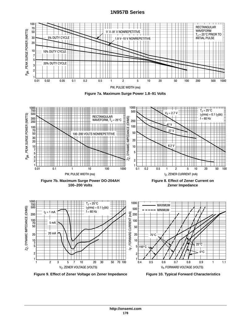
1N957B Series
http://onsemi.com178
100
7050
30
20
10
7
5
3
2
10.01 0.02 0.05 0.1 0.2 0.5 1 2 5 10 20 50 100 200 500 1000
P pk
, PE
AK
SU
RG
E P
OW
ER
(W
AT
TS
)
PW, PULSE WIDTH (ms)
5% DUTY CYCLE
10% DUTY CYCLE
20% DUTY CYCLE
11V-91V NONREPETITIVE
1.8V-10V NONREPETITIVE
RECTANGULARWAVEFORMTJ=25°C PRIOR TOINITIAL PULSE
Figure 7a. Maximum Surge Power 1.8–91 Volts
1000700500
300200
1007050
3020
107532
10.01 0.1 1 10 100 1000
P pk
, PE
AK
SU
RG
E P
OW
ER
(W
AT
TS
)
PW, PULSE WIDTH (ms)
Figure 7b. Maximum Surge Power DO-204AH100–200 Volts
1000500
200
100
50
20
10
1
2
5
0.1 0.2 0.5 1 2 5 10 20 50 100
IZ, ZENER CURRENT (mA)
Figure 8. Effect of Zener Current onZener Impedance
Z Z, D
YN
AM
IC IM
PE
DA
NC
E (
OH
MS
)
Z Z, D
YN
AM
IC IM
PE
DA
NC
E (
OH
MS
)
1000700500
200
1007050
20
1075
2
11 2 3 5 7 10 20 30 50 70 100
VZ, ZENER VOLTAGE (VOLTS)
Figure 9. Effect of Zener Voltage on Zener Impedance Figure 10. Typical Forward Characteristics
RECTANGULARWAVEFORM, TJ=25°C
100-200VOLTS NONREPETITIVE
TJ=25°C
iZ(rms)=0.1 IZ(dc)
f=60HzIZ=1mA
5mA
20mA
TJ=25°C
iZ(rms)=0.1 IZ(dc)
f=60Hz
VZ=2.7V
47V
27V
6.2V
VF, FORWARD VOLTAGE (VOLTS)
0.4 0.5 0.6 0.7 0.8 0.9 1 1.1
1000
500
200
100
50
20
10
5
2
1
I F, F
OR
WA
RD
CU
RR
EN
T (m
A) MINIMUM
MAXIMUM
150°C
75°C
0°C
25°C

1N957B Series
http://onsemi.com179
Figure 11. Zener Voltage versus Zener Current — V Z = 1 thru 16 Volts
VZ, ZENER VOLTAGE (VOLTS)
I Z, Z
EN
ER
CU
RR
EN
T (m
A)
20
10
1
0.1
0.011 2 3 4 5 6 7 8 9 10 11 12 13 14 15 16
TA=25°
Figure 12. Zener Voltage versus Zener Current — V Z = 15 thru 30 Volts
VZ, ZENER VOLTAGE (VOLTS)
15 16 17 18 19 20 21 22 23 24 25 26 27 28 29 30
10
1
0.1
0.01
TA=25°
I Z, Z
EN
ER
CU
RR
EN
T (m
A)

1N957B Series
http://onsemi.com180
Figure 13. Zener Voltage versus Zener Current — V Z = 30 thru 105 Volts
VZ, ZENER VOLTAGE (VOLTS)
10
1
0.1
0.0130 35 40 45 50 55 60 70 75 80 85 90 95 100
Figure 14. Zener Voltage versus Zener Current — V Z = 110 thru 220 Volts
VZ, ZENER VOLTAGE (VOLTS)
110 120 130 140 150 160 170 180 190 200 210 220 230 240 250 260
10
1
0.1
0.01
TA=25°
65 105
I Z, Z
EN
ER
CU
RR
EN
T (m
A)
I Z, Z
EN
ER
CU
RR
EN
T (m
A)

Semiconductor Components Industries, LLC, 2001
May, 2001 – Rev. 1181 Publication Order Number:
1N5985B/D
1N5985B Series
500 mW DO-35 HermeticallySealed Glass Zener VoltageRegulators
This is a complete series of 500 mW Zener diodes with limits andexcellent operating characteristics that reflect the superior capabilitiesof silicon–oxide passivated junctions. All this in an axial–leadhermetically sealed glass package that offers protection in all commonenvironmental conditions.
Specification Features:• Zener Voltage Range – 2.4 V to 20 V
• ESD Rating of Class 3 (>16 KV) per Human Body Model
• DO–204AH (DO–35) Package – Smaller than ConventionalDO–204AA Package
• Double Slug Type Construction
• Metallurgical Bonded Construction
Mechanical Characteristics:CASE: Double slug type, hermetically sealed glassFINISH: All external surfaces are corrosion resistant and leads arereadily solderableMAXIMUM LEAD TEMPERATURE FOR SOLDERING PURPOSES:230°C, 1/16″ from the case for 10 secondsPOLARITY: Cathode indicated by polarity bandMOUNTING POSITION: Any
MAXIMUM RATINGS (Note 1.)
Rating Symbol Value Unit
Max. Steady State Power Dissipation@ TL ≤ 75°C, Lead Length = 3/8″Derate above 75°C
PD 500
4.0
mW
mW/°C
Operating and StorageTemperature Range
TJ, Tstg –65 to+200
°C
1. Some part number series have lower JEDEC registered ratings.
Device Package Shipping
ORDERING INFORMATION
1NxxxxB Axial Lead 3000 Units/Box
1NxxxxBRL Axial Lead
AXIAL LEADCASE 299
GLASS
http://onsemi.com
5000/Tape & Reel
Cathode Anode
1NxxxxBRL2 * Axial Lead 5000/Tape & Reel
1NxxxxBTA Axial Lead 5000/Ammo Pack
* The “2” suffix refers to 26 mm tape spacing. Polarity band up with cathode lead off first Polarity band down with cathode lead off first
L1NxxxxBYWW
L = Assembly Location1NxxxxB = Device Code
= (See Table Next Page)Y = YearWW = Work Week
1NxxxxBTA2 * Axial Lead 5000/Tape & Reel
1NxxxxBRR1 Axial Lead 3000/Tape & Reel
1NxxxxBRR2 Axial Lead 3000/Tape & Reel
MARKING DIAGRAM
Devices listed in bold, italic are ON SemiconductorPreferred devices. Preferred devices are recommendedchoices for future use and best overall value.
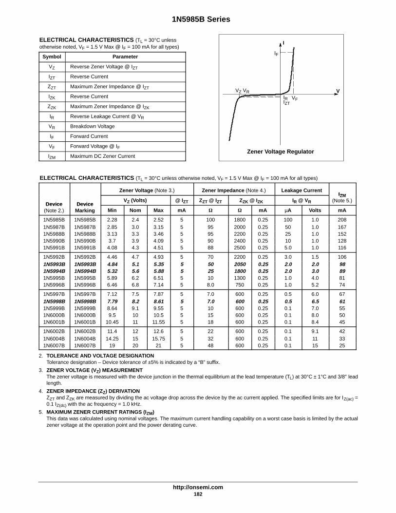
Zener Voltage Regulator
IF
V
I
IRIZT
VRVZ
VF
1N5985B Series
http://onsemi.com182
ELECTRICAL CHARACTERISTICS (TL = 30°C unlessotherwise noted, VF = 1.5 V Max @ IF = 100 mA for all types)
Symbol Parameter
VZ Reverse Zener Voltage @ IZT
IZT Reverse Current
ZZT Maximum Zener Impedance @ IZT
IZK Reverse Current
ZZK Maximum Zener Impedance @ IZK
IR Reverse Leakage Current @ VR
VR Breakdown Voltage
IF Forward Current
VF Forward Voltage @ IF
IZM Maximum DC Zener Current
ELECTRICAL CHARACTERISTICS (TL = 30°C unless otherwise noted, VF = 1.5 V Max @ IF = 100 mA for all types)
Zener Voltage (Note 3.) Zener Impedance (Note 4.) Leakage CurrentIZM
Device DeviceVZ (Volts) @ IZT ZZT @ IZT ZZK @ IZK IR @ VR
IZM(Note 5.)
Device(Note 2.)
DeviceMarking Min Nom Max mA mA µA Volts mA
1N5985B 1N5985B 2.28 2.4 2.52 5 100 1800 0.25 100 1.0 2081N5987B 1N5987B 2.85 3.0 3.15 5 95 2000 0.25 50 1.0 1671N5988B 1N5988B 3.13 3.3 3.46 5 95 2200 0.25 25 1.0 1521N5990B 1N5990B 3.7 3.9 4.09 5 90 2400 0.25 10 1.0 1281N5991B 1N5991B 4.08 4.3 4.51 5 88 2500 0.25 5.0 1.0 116
1N5992B 1N5992B 4.46 4.7 4.93 5 70 2200 0.25 3.0 1.5 1061N5993B 1N5993B 4.84 5.1 5.35 5 50 2050 0.25 2.0 2.0 981N5994B 1N5994B 5.32 5.6 5.88 5 25 1800 0.25 2.0 3.0 891N5995B 1N5995B 5.89 6.2 6.51 5 10 1300 0.25 1.0 4.0 811N5996B 1N5996B 6.46 6.8 7.14 5 8.0 750 0.25 1.0 5.2 74
1N5997B 1N5997B 7.12 7.5 7.87 5 7.0 600 0.25 0.5 6.0 671N5998B 1N5998B 7.79 8.2 8.61 5 7.0 600 0.25 0.5 6.5 611N5999B 1N5999B 8.64 9.1 9.55 5 10 600 0.25 0.1 7.0 551N6000B 1N6000B 9.5 10 10.5 5 15 600 0.25 0.1 8.0 501N6001B 1N6001B 10.45 11 11.55 5 18 600 0.25 0.1 8.4 45
1N6002B 1N6002B 11.4 12 12.6 5 22 600 0.25 0.1 9.1 421N6004B 1N6004B 14.25 15 15.75 5 32 600 0.25 0.1 11 331N6007B 1N6007B 19 20 21 5 48 600 0.25 0.1 15 25
2. TOLERANCE AND VOLTAGE DESIGNATIONTolerance designation – Device tolerance of ±5% is indicated by a “B” suffix.
3. ZENER VOLTAGE (VZ) MEASUREMENTThe zener voltage is measured with the device junction in the thermal equilibrium at the lead temperature (TL) at 30°C ± 1°C and 3/8″ leadlength.
4. ZENER IMPEDANCE (ZZ) DERIVATIONZZT and ZZK are measured by dividing the ac voltage drop across the device by the ac current applied. The specified limits are for IZ(ac) =0.1 IZ(dc) with the ac frequency = 1.0 kHz.
5. MAXIMUM ZENER CURRENT RATINGS (IZM)This data was calculated using nominal voltages. The maximum current handling capability on a worst case basis is limited by the actualzener voltage at the operation point and the power derating curve.

1N5985B Series
http://onsemi.com183
0.7
0.6
0.5
0.4
0.3
0.2
0.1
00 20 40 60 80 100 120 140 160 180 200
TL, LEAD TEMPERATURE (°C)
Figure 1. Steady State Power Derating
HEATSINKS
3/8" 3/8"
PD
, ST
EA
DY
STA
TE
PO
WE
R D
ISS
IPA
TIO
N (
WA
TT
S)

1N5985B Series
http://onsemi.com184
APPLICATION NOTE — ZENER VOLTAGE
Since the actual voltage available from a given zenerdiode is temperature dependent, it is necessary to determinejunction temperature under any set of operating conditionsin order to calculate its value. The following procedure isrecommended:
Lead Temperature, TL, should be determined from:
TL = θLAPD + TA.
θLA is the lead-to-ambient thermal resistance (°C/W) and PDis the power dissipation. The value for θLA will vary anddepends on the device mounting method. θLA is generally 30to 40°C/W for the various clips and tie points in common useand for printed circuit board wiring.
The temperature of the lead can also be measured using athermocouple placed on the lead as close as possible to thetie point. The thermal mass connected to the tie point isnormally large enough so that it will not significantlyrespond to heat surges generated in the diode as a result ofpulsed operation once steady-state conditions are achieved.Using the measured value of TL, the junction temperaturemay be determined by:
TJ = TL + ∆TJL.
∆TJL is the increase in junction temperature above the leadtemperature and may be found from Figure 2 for dc power:
∆TJL = θJLPD.
For worst-case design, using expected limits of IZ, limitsof PD and the extremes of TJ(∆TJ) may be estimated.Changes in voltage, VZ, can then be found from:
∆V = θVZTJ.
θVZ, the zener voltage temperature coefficient, is foundfrom Figures 4 and 5.
Under high power-pulse operation, the zener voltage willvary with time and may also be affected significantly by thezener resistance. For best regulation, keep currentexcursions as low as possible.
Surge limitations are given in Figure 7. They are lowerthan would be expected by considering only junctiontemperature, as current crowding effects cause temperaturesto be extremely high in small spots, resulting in devicedegradation should the limits of Figure 7 be exceeded.
L L
500
400
300
200
100
00 0.2 0.4 0.6 0.8 1
2.4-60V
62-200V
L, LEAD LENGTH TO HEAT SINK (INCH)JL, J
UN
CT
ION
TO
LE
AD
TH
ER
MA
L R
ES
ISTA
NC
E (
C/W
)θ
°
Figure 2. Typical Thermal Resistance
TYPICAL LEAKAGE CURRENTAT 80% OF NOMINALBREAKDOWN VOLTAGE
+25°C
+125°C
100070005000
2000
1000700500
200
1007050
20
1075
2
10.70.5
0.2
0.10.070.05
0.02
0.010.0070.005
0.002
0.0013 4 5 6 7 8 9 10 11 12 13 14 15
VZ, NOMINAL ZENER VOLTAGE (VOLTS)
I, L
EA
KA
GE
CU
RR
EN
T (
A)
µR
Figure 3. Typical Leakage Current

1N5985B Series
http://onsemi.com185
+12
+10
+8
+6
+4
+2
0
-2
-42 3 4 5 6 7 8 9 10 11 12
VZ, ZENER VOLTAGE (VOLTS)
Figure 4a. Range for Units to 12 Volts
VZ@IZT(NOTE 2)
RANGE
TEMPERATURE COEFFICIENTS(–55°C to +150°C temperature range; 90% of the units are in the ranges indicated.)
100
7050
30
20
10
7
5
3
2
12 3 4 5 6 7 8 9 10 11 12 10 20 30 50 70 100
VZ, ZENER VOLTAGE (VOLTS)
Figure 4b. Range for Units 12 to 100 Volts
RANGE VZ@IZ(NOTE 2)
120 130 140 150 160 170 180 190 200
200
180
160
140
120
100
VZ, ZENER VOLTAGE (VOLTS)
Figure 4c. Range for Units 120 to 200 Volts
VZ@IZT(NOTE 2)
+6
+4
+2
0
-2
-43 4 5 6 7 8
VZ, ZENER VOLTAGE (VOLTS)
Figure 5. Effect of Zener Current
NOTE: BELOW 3 VOLTS AND ABOVE 8 VOLTSNOTE: CHANGES IN ZENER CURRENT DO NOTNOTE: AFFECT TEMPERATURE COEFFICIENTS
1mA
0.01mA
VZ@IZTA=25°C
1000
C, C
APA
CIT
AN
CE
(pF
)
500
200
100
50
20
10
5
2
11 2 5 10 20 50 100
VZ, ZENER VOLTAGE (VOLTS)
Figure 6a. Typical Capacitance 2.4–100 Volts
TA=25°C
0V BIAS
1V BIAS
50% OFVZBIAS
10070
50
30
20
10
75
3
2
1120 140 160 180 190 200 220
VZ, ZENER VOLTAGE (VOLTS)
Figure 6b. Typical Capacitance 120–200 Volts
TA=25°C
1VOLTBIAS
50% OF VZBIAS
0 BIAS
θVZ
, TE
MP
ER
ATU
RE
CO
EF
FIC
IEN
T (m
V/°
C)
20mA
C, C
APA
CIT
AN
CE
(pF
)θV
Z, T
EM
PE
RAT
UR
E C
OE
FF
ICIE
NT
(mV
/°C
)θV
Z, T
EM
PE
RAT
UR
E C
OE
FF
ICIE
NT
(mV
/°C
)
θVZ
, TE
MP
ER
ATU
RE
CO
EF
FIC
IEN
T (m
V/°
C)

1N5985B Series
http://onsemi.com186
100
7050
30
20
10
7
5
3
2
10.01 0.02 0.05 0.1 0.2 0.5 1 2 5 10 20 50 100 200 500 1000
P pk
, PE
AK
SU
RG
E P
OW
ER
(W
AT
TS
)
PW, PULSE WIDTH (ms)
5% DUTY CYCLE
10% DUTY CYCLE
20% DUTY CYCLE
11V-91V NONREPETITIVE
1.8V-10V NONREPETITIVE
RECTANGULARWAVEFORMTJ=25°C PRIOR TOINITIAL PULSE
Figure 7a. Maximum Surge Power 1.8–91 Volts
1000700500
300200
1007050
3020
107532
10.01 0.1 1 10 100 1000
P pk
, PE
AK
SU
RG
E P
OW
ER
(W
AT
TS
)
PW, PULSE WIDTH (ms)
Figure 7b. Maximum Surge Power DO-204AH100–200 Volts
1000500
200
100
50
20
10
1
2
5
0.1 0.2 0.5 1 2 5 10 20 50 100
IZ, ZENER CURRENT (mA)
Figure 8. Effect of Zener Current onZener Impedance
Z Z, D
YN
AM
IC IM
PE
DA
NC
E (
OH
MS
)
Z Z, D
YN
AM
IC IM
PE
DA
NC
E (
OH
MS
)
1000700500
200
1007050
20
1075
2
11 2 3 5 7 10 20 30 50 70 100
VZ, ZENER VOLTAGE (VOLTS)
Figure 9. Effect of Zener Voltage on Zener Impedance Figure 10. Typical Forward Characteristics
RECTANGULARWAVEFORM, TJ=25°C
100-200VOLTS NONREPETITIVE
TJ=25°C
iZ(rms)=0.1 IZ(dc)
f=60HzIZ=1mA
5mA
20mA
TJ=25°C
iZ(rms)=0.1 IZ(dc)
f=60Hz
VZ=2.7V
47V
27V
6.2V
VF, FORWARD VOLTAGE (VOLTS)
0.4 0.5 0.6 0.7 0.8 0.9 1 1.1
1000
500
200
100
50
20
10
5
2
1
I F, F
OR
WA
RD
CU
RR
EN
T (m
A) MINIMUM
MAXIMUM
150°C
75°C
0°C
25°C

1N5985B Series
http://onsemi.com187
Figure 11. Zener Voltage versus Zener Current — V Z = 1 thru 16 Volts
VZ, ZENER VOLTAGE (VOLTS)
I Z, Z
EN
ER
CU
RR
EN
T (m
A)
20
10
1
0.1
0.011 2 3 4 5 6 7 8 9 10 11 12 13 14 15 16
TA=25°
Figure 12. Zener Voltage versus Zener Current — V Z = 15 thru 30 Volts
VZ, ZENER VOLTAGE (VOLTS)
15 16 17 18 19 20 21 22 23 24 25 26 27 28 29 30
10
1
0.1
0.01
TA=25°
I Z, Z
EN
ER
CU
RR
EN
T (m
A)

1N5985B Series
http://onsemi.com188
Figure 13. Zener Voltage versus Zener Current — V Z = 30 thru 105 Volts
VZ, ZENER VOLTAGE (VOLTS)
10
1
0.1
0.0130 35 40 45 50 55 60 70 75 80 85 90 95 100
Figure 14. Zener Voltage versus Zener Current — V Z = 110 thru 220 Volts
VZ, ZENER VOLTAGE (VOLTS)
110 120 130 140 150 160 170 180 190 200 210 220 230 240 250 260
10
1
0.1
0.01
TA=25°
65 105
I Z, Z
EN
ER
CU
RR
EN
T (m
A)
I Z, Z
EN
ER
CU
RR
EN
T (m
A)

Semiconductor Components Industries, LLC, 2001
May, 2001 – Rev. 1189 Publication Order Number:
BZX79C2V4RL/D
BZX79C2V4RL Series
500 mW DO-35 HermeticallySealed Glass Zener VoltageRegulators
This is a complete series of 500 mW Zener diodes with limits andexcellent operating characteristics that reflect the superior capabilitiesof silicon–oxide passivated junctions. All this in an axial–leadhermetically sealed glass package that offers protection in all commonenvironmental conditions.
Specification Features:• Zener Voltage Range – 2.4 V to 33 V
• ESD Rating of Class 3 (>16 KV) per Human Body Model
• DO–204AH (DO–35) Package – Smaller than ConventionalDO–204AA Package
• Double Slug Type Construction
• Metallurgical Bonded Construction
Mechanical Characteristics:CASE: Double slug type, hermetically sealed glassFINISH: All external surfaces are corrosion resistant and leads arereadily solderableMAXIMUM LEAD TEMPERATURE FOR SOLDERING PURPOSES:230°C, 1/16″ from the case for 10 secondsPOLARITY: Cathode indicated by polarity bandMOUNTING POSITION: Any
MAXIMUM RATINGS (Note 1.)
Rating Symbol Value Unit
Max. Steady State Power Dissipation@ TL ≤ 75°C, Lead Length = 3/8″Derate above 75°C
PD 500
4.0
mW
mW/°C
Operating and StorageTemperature Range
TJ, Tstg –65 to+200
°C
1. Some part number series have lower JEDEC registered ratings.
Device Package Shipping
ORDERING INFORMATION
BZX79CxxxRL Axial Lead 5000/Tape & Reel
BZX79CxxxRL2* Axial Lead
AXIAL LEADCASE 299
GLASS
http://onsemi.com
5000/Tape & Reel
Cathode Anode
* The “2” suffix refers to 26 mm tape spacing.
L79CxxxYWW
L = Assembly Location79Cxxx = Device Code
= (See Table Next Page)Y = YearWW = Work Week
MARKING DIAGRAM

Zener Voltage Regulator
IF
V
I
IRIZT
VRVZ
VF
BZX79C2V4RL Series
http://onsemi.com190
ELECTRICAL CHARACTERISTICS (TL = 30°C unlessotherwise noted, VF = 1.5 V Max @ IF = 100 mA for all types)
Symbol Parameter
VZ Reverse Zener Voltage @ IZT
IZT Reverse Current
ZZT Maximum Zener Impedance @ IZT
VBR Temperature Coefficient of VBR (Typical)
IR Reverse Leakage Current (TA = 25°C) @ VR
VR Breakdown Voltage
IF Forward Current
VF Forward Voltage @ IF
C Capacitance (Typical)
ELECTRICAL CHARACTERISTICS (TL = 30°C unless otherwise noted, VF = 1.5 V Max @ IF = 100 mA for all types)
Zener Voltage (Note 3.) ZZT (Note 4.)@ I
Leakage Current VBR CV 0
Device DeviceVZ (Volts) @ IZT
@ IZT(f = 1.0 kHz) IR @ VR mV/C
VZ = 0,f = 1.0 MHz
Device(Note 2.)
DeviceMarking Min Nom Max mA µA Volts Min Max pF
BZX79C2V4RL 79C2V4 2.28 2.4 2.52 5 100 100 1 –3.5 0 255BZX79C2V7RL 79C2V7 2.57 2.7 2.84 5 100 75 1 –3.5 0 230BZX79C3V0RL 79C3V0 2.85 3.0 3.15 5 95 50 1 –3.5 0 215BZX79C3V3RL 79C3V3 3.14 3.3 3.47 5 95 25 1 –3.5 0 200BZX79C3V6RL 79C3V6 3.42 3.6 3.78 5 90 15 1 –3.5 0 185
BZX79C3V9RL 79C3V9 3.71 3.9 4.10 5 90 10 1 –3.5 0.3 175BZX79C4V7RL 79C4V7 4.47 4.7 4.94 5 80 3 2 –3.5 0.2 130BZX79C5V1RL 79C5V1 4.85 5.1 5.36 5 60 2 2 –2.7 1.2 110BZX79C5V6RL 79C5V6 5.32 5.6 5.88 5 40 1 2 –2.0 2.5 95BZX79C6V2RL 79C6V2 5.89 6.2 6.51 5 10 3 4 0.4 3.7 90
BZX79C6V8RL 79C6V8 6.46 6.8 7.19 5 15 2 4 1.2 4.5 85BZX79C7V5RL 79C7V5 7.13 7.5 7.88 5 15 1 5 2.5 5.3 80BZX79C8V2RL 79C8V2 7.79 8.2 8.61 5 15 0.7 5 3.2 6.2 75BZX79C10RL 79C10 9.5 10 10.5 5 20 0.2 7 4.5 8.0 70BZX79C12RL 79C12 11.4 12 12.6 5 25 0.1 8 6.0 10 65
BZX79C15RL 79C15 14.25 15 15.75 5 30 0.05 10.5 9.2 13 55BZX79C16RL 79C16 15.2 16 16.8 5 40 0.05 11.2 10.4 14 52BZX79C18RL 79C18 17.1 18 18.9 5 45 0.05 12.6 12.9 16 47BZX79C22RL 79C22 20.9 22 23.1 5 55 0.05 15.4 16.4 20 34BZX79C24RL 79C24 22.8 24 25.2 5 70 0.05 16.8 18.4 22 33
BZX79C27RL 79C27 25.65 27 28.35 5 80 0.05 18.9 – 23.5 30BZX79C30RL 79C30 28.5 30 31.5 5 80 0.05 21 – 26 27BZX79C33RL 79C33 31.35 33 34.65 5 80 0.05 23.1 – 29 25
2. TOLERANCE AND VOLTAGE DESIGNATIONTolerance designation – the type numbers listed have zener voltage min/max limits as shown.
3. REVERSE ZENER VOLTAGE (VZ) MEASUREMENTReverse zener voltage is measured under pulse conditions such that TJ is no more than 2°C above TA.
4. ZENER IMPEDANCE (ZZ) DERIVATIONZZT and ZZK are measured by dividing the ac voltage drop across the device by the ac current applied. The specified limits are for IZ(ac) =0.1 IZ(dc) with the ac frequency = 1.0 kHz.

BZX79C2V4RL Series
http://onsemi.com191
0.7
0.6
0.5
0.4
0.3
0.2
0.1
00 20 40 60 80 100 120 140 160 180 200
TL, LEAD TEMPERATURE (°C)
Figure 1. Steady State Power Derating
HEATSINKS
3/8" 3/8"
PD
, ST
EA
DY
STA
TE
PO
WE
R D
ISS
IPA
TIO
N (
WA
TT
S)

BZX79C2V4RL Series
http://onsemi.com192
APPLICATION NOTE — ZENER VOLTAGE
Since the actual voltage available from a given zenerdiode is temperature dependent, it is necessary to determinejunction temperature under any set of operating conditionsin order to calculate its value. The following procedure isrecommended:
Lead Temperature, TL, should be determined from:
TL = θLAPD + TA.
θLA is the lead-to-ambient thermal resistance (°C/W) and PDis the power dissipation. The value for θLA will vary anddepends on the device mounting method. θLA is generally 30to 40°C/W for the various clips and tie points in common useand for printed circuit board wiring.
The temperature of the lead can also be measured using athermocouple placed on the lead as close as possible to thetie point. The thermal mass connected to the tie point isnormally large enough so that it will not significantlyrespond to heat surges generated in the diode as a result ofpulsed operation once steady-state conditions are achieved.Using the measured value of TL, the junction temperaturemay be determined by:
TJ = TL + ∆TJL.
∆TJL is the increase in junction temperature above the leadtemperature and may be found from Figure 2 for dc power:
∆TJL = θJLPD.
For worst-case design, using expected limits of IZ, limitsof PD and the extremes of TJ(∆TJ) may be estimated.Changes in voltage, VZ, can then be found from:
∆V = θVZTJ.
θVZ, the zener voltage temperature coefficient, is foundfrom Figures 4 and 5.
Under high power-pulse operation, the zener voltage willvary with time and may also be affected significantly by thezener resistance. For best regulation, keep currentexcursions as low as possible.
Surge limitations are given in Figure 7. They are lowerthan would be expected by considering only junctiontemperature, as current crowding effects cause temperaturesto be extremely high in small spots, resulting in devicedegradation should the limits of Figure 7 be exceeded.
L L
500
400
300
200
100
00 0.2 0.4 0.6 0.8 1
2.4-60V
62-200V
L, LEAD LENGTH TO HEAT SINK (INCH)JL, J
UN
CT
ION
TO
LE
AD
TH
ER
MA
L R
ES
ISTA
NC
E (
C/W
)θ
°
Figure 2. Typical Thermal Resistance
TYPICAL LEAKAGE CURRENTAT 80% OF NOMINALBREAKDOWN VOLTAGE
+25°C
+125°C
100070005000
2000
1000700500
200
1007050
20
1075
2
10.70.5
0.2
0.10.070.05
0.02
0.010.0070.005
0.002
0.0013 4 5 6 7 8 9 10 11 12 13 14 15
VZ, NOMINAL ZENER VOLTAGE (VOLTS)
I, L
EA
KA
GE
CU
RR
EN
T (
A)
µR
Figure 3. Typical Leakage Current

BZX79C2V4RL Series
http://onsemi.com193
+12
+10
+8
+6
+4
+2
0
-2
-42 3 4 5 6 7 8 9 10 11 12
VZ, ZENER VOLTAGE (VOLTS)
Figure 4a. Range for Units to 12 Volts
VZ@IZT(NOTE 2)
RANGE
TEMPERATURE COEFFICIENTS(–55°C to +150°C temperature range; 90% of the units are in the ranges indicated.)
100
7050
30
20
10
7
5
3
2
12 3 4 5 6 7 8 9 10 11 12 10 20 30 50 70 100
VZ, ZENER VOLTAGE (VOLTS)
Figure 4b. Range for Units 12 to 100 Volts
RANGE VZ@IZ(NOTE 2)
120 130 140 150 160 170 180 190 200
200
180
160
140
120
100
VZ, ZENER VOLTAGE (VOLTS)
Figure 4c. Range for Units 120 to 200 Volts
VZ@IZT(NOTE 2)
+6
+4
+2
0
-2
-43 4 5 6 7 8
VZ, ZENER VOLTAGE (VOLTS)
Figure 5. Effect of Zener Current
NOTE: BELOW 3 VOLTS AND ABOVE 8 VOLTSNOTE: CHANGES IN ZENER CURRENT DO NOTNOTE: AFFECT TEMPERATURE COEFFICIENTS
1mA
0.01mA
VZ@IZTA=25°C
1000
C, C
APA
CIT
AN
CE
(pF
)
500
200
100
50
20
10
5
2
11 2 5 10 20 50 100
VZ, ZENER VOLTAGE (VOLTS)
Figure 6a. Typical Capacitance 2.4–100 Volts
TA=25°C
0V BIAS
1V BIAS
50% OFVZBIAS
10070
50
30
20
10
75
3
2
1120 140 160 180 190 200 220
VZ, ZENER VOLTAGE (VOLTS)
Figure 6b. Typical Capacitance 120–200 Volts
TA=25°C
1VOLTBIAS
50% OF VZBIAS
0 BIAS
θVZ
, TE
MP
ER
ATU
RE
CO
EF
FIC
IEN
T (m
V/°
C)
20mA
C, C
APA
CIT
AN
CE
(pF
)θV
Z, T
EM
PE
RAT
UR
E C
OE
FF
ICIE
NT
(mV
/°C
)θV
Z, T
EM
PE
RAT
UR
E C
OE
FF
ICIE
NT
(mV
/°C
)
θVZ
, TE
MP
ER
ATU
RE
CO
EF
FIC
IEN
T (m
V/°
C)

BZX79C2V4RL Series
http://onsemi.com194
100
7050
30
20
10
7
5
3
2
10.01 0.02 0.05 0.1 0.2 0.5 1 2 5 10 20 50 100 200 500 1000
P pk
, PE
AK
SU
RG
E P
OW
ER
(W
AT
TS
)
PW, PULSE WIDTH (ms)
5% DUTY CYCLE
10% DUTY CYCLE
20% DUTY CYCLE
11V-91V NONREPETITIVE
1.8V-10V NONREPETITIVE
RECTANGULARWAVEFORMTJ=25°C PRIOR TOINITIAL PULSE
Figure 7a. Maximum Surge Power 1.8–91 Volts
1000700500
300200
1007050
3020
107532
10.01 0.1 1 10 100 1000
P pk
, PE
AK
SU
RG
E P
OW
ER
(W
AT
TS
)
PW, PULSE WIDTH (ms)
Figure 7b. Maximum Surge Power DO-204AH100–200 Volts
1000500
200
100
50
20
10
1
2
5
0.1 0.2 0.5 1 2 5 10 20 50 100
IZ, ZENER CURRENT (mA)
Figure 8. Effect of Zener Current onZener Impedance
Z Z, D
YN
AM
IC IM
PE
DA
NC
E (
OH
MS
)
Z Z, D
YN
AM
IC IM
PE
DA
NC
E (
OH
MS
)
1000700500
200
1007050
20
1075
2
11 2 3 5 7 10 20 30 50 70 100
VZ, ZENER VOLTAGE (VOLTS)
Figure 9. Effect of Zener Voltage on Zener Impedance Figure 10. Typical Forward Characteristics
RECTANGULARWAVEFORM, TJ=25°C
100-200VOLTS NONREPETITIVE
TJ=25°C
iZ(rms)=0.1 IZ(dc)
f=60HzIZ=1mA
5mA
20mA
TJ=25°C
iZ(rms)=0.1 IZ(dc)
f=60Hz
VZ=2.7V
47V
27V
6.2V
VF, FORWARD VOLTAGE (VOLTS)
0.4 0.5 0.6 0.7 0.8 0.9 1 1.1
1000
500
200
100
50
20
10
5
2
1
I F, F
OR
WA
RD
CU
RR
EN
T (m
A) MINIMUM
MAXIMUM
150°C
75°C
0°C
25°C

BZX79C2V4RL Series
http://onsemi.com195
Figure 11. Zener Voltage versus Zener Current — V Z = 1 thru 16 Volts
VZ, ZENER VOLTAGE (VOLTS)
I Z, Z
EN
ER
CU
RR
EN
T (m
A)
20
10
1
0.1
0.011 2 3 4 5 6 7 8 9 10 11 12 13 14 15 16
TA=25°
Figure 12. Zener Voltage versus Zener Current — V Z = 15 thru 30 Volts
VZ, ZENER VOLTAGE (VOLTS)
15 16 17 18 19 20 21 22 23 24 25 26 27 28 29 30
10
1
0.1
0.01
TA=25°
I Z, Z
EN
ER
CU
RR
EN
T (m
A)

BZX79C2V4RL Series
http://onsemi.com196
Figure 13. Zener Voltage versus Zener Current — V Z = 30 thru 105 Volts
VZ, ZENER VOLTAGE (VOLTS)
10
1
0.1
0.0130 35 40 45 50 55 60 70 75 80 85 90 95 100
Figure 14. Zener Voltage versus Zener Current — V Z = 110 thru 220 Volts
VZ, ZENER VOLTAGE (VOLTS)
110 120 130 140 150 160 170 180 190 200 210 220 230 240 250 260
10
1
0.1
0.01
TA=25°
65 105
I Z, Z
EN
ER
CU
RR
EN
T (m
A)
I Z, Z
EN
ER
CU
RR
EN
T (m
A)

Semiconductor Components Industries, LLC, 2001
May, 2001 – Rev. 1197 Publication Order Number:
1N4678/D
1N4678 Series
500 mW DO-35 HermeticallySealed Glass Zener VoltageRegulators
This is a complete series of 500 mW Zener diodes with limits andexcellent operating characteristics that reflect the superior capabilitiesof silicon–oxide passivated junctions. All this in an axial–leadhermetically sealed glass package that offers protection in all commonenvironmental conditions.
Specification Features:• Zener Voltage Range – 1.8 V to 27 V
• ESD Rating of Class 3 (>16 KV) per Human Body Model
• DO–204AH (DO–35) Package – Smaller than ConventionalDO–204AA Package
• Double Slug Type Construction
• Metallurgical Bonded Construction
Mechanical Characteristics:CASE: Double slug type, hermetically sealed glassFINISH: All external surfaces are corrosion resistant and leads arereadily solderableMAXIMUM LEAD TEMPERATURE FOR SOLDERING PURPOSES:230°C, 1/16″ from the case for 10 secondsPOLARITY: Cathode indicated by polarity bandMOUNTING POSITION: Any
MAXIMUM RATINGS (Note 1.)
Rating Symbol Value Unit
Max. Steady State Power Dissipation@ TL ≤ 75°C, Lead Length = 3/8″Derate above 75°C
PD 500
4.0
mW
mW/°C
Operating and StorageTemperature Range
TJ, Tstg –65 to+200
°C
1. Some part number series have lower JEDEC registered ratings.
Device Package Shipping
ORDERING INFORMATION
1N4xxx Axial Lead 3000 Units/Box
1N4xxxRL Axial Lead
AXIAL LEADCASE 299
GLASS
http://onsemi.com
5000/Tape & Reel
Cathode Anode
1N4xxxRL2 * Axial Lead 5000/Tape & Reel
1N4xxxTA Axial Lead 5000/Ammo Pack
* The “2” suffix refers to 26 mm tape spacing. Polarity band up with cathode lead off first Polarity band down with cathode lead off first
L1N4xxxYWW
L = Assembly Location1N4xxx = Device Code
= (See Table Next Page)Y = YearWW = Work Week
1N4xxxTA2 * Axial Lead 5000/Tape & Reel
1N4xxxRR1 Axial Lead 3000/Tape & Reel
1N4xxxRR2 Axial Lead 3000/Tape & Reel
MARKING DIAGRAM
Devices listed in bold, italic are ON SemiconductorPreferred devices. Preferred devices are recommendedchoices for future use and best overall value.

Zener Voltage Regulator
IF
V
I
IRIZT
VRVZ
VF
1N4678 Series
http://onsemi.com198
Low level oxide passivated zener diodes for applicationsrequiring extremely low operating currents, low leakage,and sharp breakdown voltage.
ELECTRICAL CHARACTERISTICS (TA = 25°C unlessotherwise noted, VF = 1.5 V Max @ IF = 100 mA for all types)
Symbol Parameter
VZ Reverse Zener Voltage @ IZT
IZT Reverse Current
VZ Reverse Zener Voltage Change
IZM Maximum Zener Current
IR Reverse Leakage Current @ VR
VR Breakdown Voltage
IF Forward Current
VF Forward Voltage @ IF

1N4678 Series
http://onsemi.com199
ELECTRICAL CHARACTERISTICS (TL = 30°C unless otherwise noted, VF = 1.5 V Max @ IF = 100 mA for all types)
Zener Voltage (Note 3.) Leakage Current (Note 4.)IZM VZ
Device DeviceVZ (Volts) @ IZT IR @ VR
IZM(Note 5.)
VZ(Note 6.)
Device(Note 2.)
DeviceMarking Min Nom Max A µA Max Volts mA Volts
1N4678 1N4678 1.71 1.8 1.89 50 7.5 1 120 0.71N4679 1N4679 1.9 2.0 2.1 50 5 1 110 0.71N4680 1N4680 2.09 2.2 2.31 50 5 1 100 0.751N4681 1N4681 2.28 2.4 2.52 50 2 1 95 0.81N4682 1N4682 2.565 2.7 2.835 50 1 1 90 0.85
1N4683 1N4683 2.85 3.0 3.15 50 0.8 1 85 0.91N4684 1N4684 3.135 3.3 3.465 50 7.5 1.5 80 0.951N4685 1N4685 3.42 3.6 3.78 50 7.5 2 75 0.951N4686 1N4686 3.705 3.9 4.095 50 5.0 2 70 0.971N4687 1N4687 4.085 4.3 4.515 50 4.0 2 65 0.99
1N4688 1N4688 4.465 4.7 4.935 50 10 3 60 0.991N4689 1N4689 4.845 5.1 5.355 50 10 3 55 0.971N4690 1N4690 5.32 5.6 5.88 50 10 4 50 0.961N4691 1N4691 5.89 6.2 6.51 50 10 5 45 0.951N4692 1N4692 6.46 6.8 7.14 50 10 5.1 35 0.9
1N4693 1N4693 7.125 7.5 7.875 50 10 5.7 31.8 0.751N4694 1N4694 7.79 8.2 8.61 50 1 6.2 29 0.51N4695 1N4695 8.265 8.7 9.135 50 1 6.6 27.4 0.11N4696 1N4696 8.645 9.1 9.555 50 1 6.9 26.2 0.081N4697 1N4697 9.5 10 10.5 50 1 7.6 24.8 0.1
1N4698 1N4698 10.45 11 11.55 50 0.05 8.4 21.6 0.111N4699 1N4699 11.4 12 12.6 50 0.05 9.1 20.4 0.121N4700 1N4700 12.35 13 13.65 50 0.05 9.8 19 0.131N4701 1N4701 13.3 14 14.7 50 0.05 10.6 17.5 0.141N4702 1N4702 14.25 15 15.75 50 0.05 11.4 16.3 0.15
1N4703 1N4703 15.2 16 16.8 50 0.05 12.1 15.4 0.161N4704 1N4704 16.15 17 17.85 50 0.05 12.9 14.5 0.171N4705 1N4705 17.1 18 18.9 50 0.05 13.6 13.2 0.181N4707 1N4707 19 20 21 50 0.01 15.2 11.9 0.21N4711 1N4711 25.65 27 28.35 50 0.01 20.4 8.8 0.27
2. TOLERANCE AND TYPE NUMBER DESIGNATION (V Z)The type numbers listed have a standard tolerance of ±5% on the nominal zener voltage.
3. ZENER VOLTAGE (VZ) MEASUREMENTThe zener voltage is measured with the device junction in the thermal equilibrium at the lead temperature (TL) at 30°C ± 1°C and 3/8″ leadlength.
4. REVERSE LEAKAGE CURRENT (I R)Reverse leakage currents are guaranteed and measured at VR shown on the table.
5. MAXIMUM ZENER CURRENT RATINGS (IZM)Maximum zener current ratings are based on maximum zener voltage of the individual units and JEDEC 250 mW rating.
6. MAXIMUM VOLTAGE CHANGE ( VZ)Voltage change is equal to the difference between VZ at 100 A and at 10 A.

1N4678 Series
http://onsemi.com200
0.7
0.6
0.5
0.4
0.3
0.2
0.1
00 20 40 60 80 100 120 140 160 180 200
TL, LEAD TEMPERATURE (°C)
Figure 1. Steady State Power Derating
HEATSINKS
3/8" 3/8"
PD
, ST
EA
DY
STA
TE
PO
WE
R D
ISS
IPA
TIO
N (
WA
TT
S)

1N4678 Series
http://onsemi.com201
APPLICATION NOTE — ZENER VOLTAGE
Since the actual voltage available from a given zenerdiode is temperature dependent, it is necessary to determinejunction temperature under any set of operating conditionsin order to calculate its value. The following procedure isrecommended:
Lead Temperature, TL, should be determined from:
TL = θLAPD + TA.
θLA is the lead-to-ambient thermal resistance (°C/W) and PDis the power dissipation. The value for θLA will vary anddepends on the device mounting method. θLA is generally 30to 40°C/W for the various clips and tie points in common useand for printed circuit board wiring.
The temperature of the lead can also be measured using athermocouple placed on the lead as close as possible to thetie point. The thermal mass connected to the tie point isnormally large enough so that it will not significantlyrespond to heat surges generated in the diode as a result ofpulsed operation once steady-state conditions are achieved.Using the measured value of TL, the junction temperaturemay be determined by:
TJ = TL + ∆TJL.
∆TJL is the increase in junction temperature above the leadtemperature and may be found from Figure 2 for dc power:
∆TJL = θJLPD.
For worst-case design, using expected limits of IZ, limitsof PD and the extremes of TJ(∆TJ) may be estimated.Changes in voltage, VZ, can then be found from:
∆V = θVZTJ.
θVZ, the zener voltage temperature coefficient, is foundfrom Figures 4 and 5.
Under high power-pulse operation, the zener voltage willvary with time and may also be affected significantly by thezener resistance. For best regulation, keep currentexcursions as low as possible.
Surge limitations are given in Figure 7. They are lowerthan would be expected by considering only junctiontemperature, as current crowding effects cause temperaturesto be extremely high in small spots, resulting in devicedegradation should the limits of Figure 7 be exceeded.
L L
500
400
300
200
100
00 0.2 0.4 0.6 0.8 1
2.4-60V
62-200V
L, LEAD LENGTH TO HEAT SINK (INCH)JL, J
UN
CT
ION
TO
LE
AD
TH
ER
MA
L R
ES
ISTA
NC
E (
C/W
)θ
°
Figure 2. Typical Thermal Resistance
TYPICAL LEAKAGE CURRENTAT 80% OF NOMINALBREAKDOWN VOLTAGE
+25°C
+125°C
100070005000
2000
1000700500
200
1007050
20
1075
2
10.70.5
0.2
0.10.070.05
0.02
0.010.0070.005
0.002
0.0013 4 5 6 7 8 9 10 11 12 13 14 15
VZ, NOMINAL ZENER VOLTAGE (VOLTS)
I, L
EA
KA
GE
CU
RR
EN
T (
A)
µR
Figure 3. Typical Leakage Current

1N4678 Series
http://onsemi.com202
+12
+10
+8
+6
+4
+2
0
-2
-42 3 4 5 6 7 8 9 10 11 12
VZ, ZENER VOLTAGE (VOLTS)
Figure 4a. Range for Units to 12 Volts
VZ@IZT(NOTE 2)
RANGE
TEMPERATURE COEFFICIENTS(–55°C to +150°C temperature range; 90% of the units are in the ranges indicated.)
100
7050
30
20
10
7
5
3
2
12 3 4 5 6 7 8 9 10 11 12 10 20 30 50 70 100
VZ, ZENER VOLTAGE (VOLTS)
Figure 4b. Range for Units 12 to 100 Volts
RANGE VZ@IZ(NOTE 2)
120 130 140 150 160 170 180 190 200
200
180
160
140
120
100
VZ, ZENER VOLTAGE (VOLTS)
Figure 4c. Range for Units 120 to 200 Volts
VZ@IZT(NOTE 2)
+6
+4
+2
0
-2
-43 4 5 6 7 8
VZ, ZENER VOLTAGE (VOLTS)
Figure 5. Effect of Zener Current
NOTE: BELOW 3 VOLTS AND ABOVE 8 VOLTSNOTE: CHANGES IN ZENER CURRENT DO NOTNOTE: AFFECT TEMPERATURE COEFFICIENTS
1mA
0.01mA
VZ@IZTA=25°C
1000
C, C
APA
CIT
AN
CE
(pF
)
500
200
100
50
20
10
5
2
11 2 5 10 20 50 100
VZ, ZENER VOLTAGE (VOLTS)
Figure 6a. Typical Capacitance 2.4–100 Volts
TA=25°C
0V BIAS
1V BIAS
50% OFVZBIAS
10070
50
30
20
10
75
3
2
1120 140 160 180 190 200 220
VZ, ZENER VOLTAGE (VOLTS)
Figure 6b. Typical Capacitance 120–200 Volts
TA=25°C
1VOLTBIAS
50% OF VZBIAS
0 BIAS
θVZ
, TE
MP
ER
ATU
RE
CO
EF
FIC
IEN
T (m
V/°
C)
20mA
C, C
APA
CIT
AN
CE
(pF
)θV
Z, T
EM
PE
RAT
UR
E C
OE
FF
ICIE
NT
(mV
/°C
)θV
Z, T
EM
PE
RAT
UR
E C
OE
FF
ICIE
NT
(mV
/°C
)
θVZ
, TE
MP
ER
ATU
RE
CO
EF
FIC
IEN
T (m
V/°
C)

1N4678 Series
http://onsemi.com203
100
7050
30
20
10
7
5
3
2
10.01 0.02 0.05 0.1 0.2 0.5 1 2 5 10 20 50 100 200 500 1000
P pk
, PE
AK
SU
RG
E P
OW
ER
(W
AT
TS
)
PW, PULSE WIDTH (ms)
5% DUTY CYCLE
10% DUTY CYCLE
20% DUTY CYCLE
11V-91V NONREPETITIVE
1.8V-10V NONREPETITIVE
RECTANGULARWAVEFORMTJ=25°C PRIOR TOINITIAL PULSE
Figure 7a. Maximum Surge Power 1.8–91 Volts
1000700500
300200
1007050
3020
107532
10.01 0.1 1 10 100 1000
P pk
, PE
AK
SU
RG
E P
OW
ER
(W
AT
TS
)
PW, PULSE WIDTH (ms)
Figure 7b. Maximum Surge Power DO-204AH100–200 Volts
1000500
200
100
50
20
10
1
2
5
0.1 0.2 0.5 1 2 5 10 20 50 100
IZ, ZENER CURRENT (mA)
Figure 8. Effect of Zener Current onZener Impedance
Z Z, D
YN
AM
IC IM
PE
DA
NC
E (
OH
MS
)
Z Z, D
YN
AM
IC IM
PE
DA
NC
E (
OH
MS
)
1000700500
200
1007050
20
1075
2
11 2 3 5 7 10 20 30 50 70 100
VZ, ZENER VOLTAGE (VOLTS)
Figure 9. Effect of Zener Voltage on Zener Impedance Figure 10. Typical Forward Characteristics
RECTANGULARWAVEFORM, TJ=25°C
100-200VOLTS NONREPETITIVE
TJ=25°C
iZ(rms)=0.1 IZ(dc)
f=60HzIZ=1mA
5mA
20mA
TJ=25°C
iZ(rms)=0.1 IZ(dc)
f=60Hz
VZ=2.7V
47V
27V
6.2V
VF, FORWARD VOLTAGE (VOLTS)
0.4 0.5 0.6 0.7 0.8 0.9 1 1.1
1000
500
200
100
50
20
10
5
2
1
I F, F
OR
WA
RD
CU
RR
EN
T (m
A) MINIMUM
MAXIMUM
150°C
75°C
0°C
25°C

1N4678 Series
http://onsemi.com204
Figure 11. Zener Voltage versus Zener Current — V Z = 1 thru 16 Volts
VZ, ZENER VOLTAGE (VOLTS)
I Z, Z
EN
ER
CU
RR
EN
T (m
A)
20
10
1
0.1
0.011 2 3 4 5 6 7 8 9 10 11 12 13 14 15 16
TA=25°
Figure 12. Zener Voltage versus Zener Current — V Z = 15 thru 30 Volts
VZ, ZENER VOLTAGE (VOLTS)
15 16 17 18 19 20 21 22 23 24 25 26 27 28 29 30
10
1
0.1
0.01
TA=25°
I Z, Z
EN
ER
CU
RR
EN
T (m
A)

1N4678 Series
http://onsemi.com205
Figure 13. Zener Voltage versus Zener Current — V Z = 30 thru 105 Volts
VZ, ZENER VOLTAGE (VOLTS)
10
1
0.1
0.0130 35 40 45 50 55 60 70 75 80 85 90 95 100
Figure 14. Zener Voltage versus Zener Current — V Z = 110 thru 220 Volts
VZ, ZENER VOLTAGE (VOLTS)
110 120 130 140 150 160 170 180 190 200 210 220 230 240 250 260
10
1
0.1
0.01
TA=25°
65 105
I Z, Z
EN
ER
CU
RR
EN
T (m
A)
I Z, Z
EN
ER
CU
RR
EN
T (m
A)

Semiconductor Components Industries, LLC, 2001
May, 2001 – Rev. 2206 Publication Order Number:
1N5221B/D
1N5221B Series
500 mW DO-35 HermeticallySealed Glass Zener VoltageRegulators
This is a complete series of 500 mW Zener diodes with limits andexcellent operating characteristics that reflect the superior capabilitiesof silicon–oxide passivated junctions. All this in an axial–leadhermetically sealed glass package that offers protection in all commonenvironmental conditions.
Specification Features:• Zener Voltage Range – 2.4 V to 91 V
• ESD Rating of Class 3 (>16 KV) per Human Body Model
• DO–204AH (DO–35) Package – Smaller than ConventionalDO–204AA Package
• Double Slug Type Construction
• Metallurgical Bonded Construction
Mechanical Characteristics:CASE: Double slug type, hermetically sealed glassFINISH: All external surfaces are corrosion resistant and leads arereadily solderableMAXIMUM LEAD TEMPERATURE FOR SOLDERING PURPOSES:230°C, 1/16″ from the case for 10 secondsPOLARITY: Cathode indicated by polarity bandMOUNTING POSITION: Any
MAXIMUM RATINGS (Note 1.)
Rating Symbol Value Unit
Max. Steady State Power Dissipation@ TL ≤ 75°C, Lead Length = 3/8″Derate above 75°C
PD 500
4.0
mW
mW/°C
Operating and StorageTemperature Range
TJ, Tstg –65 to+200
°C
1. Some part number series have lower JEDEC registered ratings.
1N52xxBTA Axial Lead 5000/Ammo Pack
1N52xxBTA2 * Axial Lead 5000/Ammo Pack
1N52xxBRR1 Axial Lead 3000/Tape & Reel
1N52xxBRR2 Axial Lead 3000/Tape & Reel
Device Package Shipping
ORDERING INFORMATION
1N52xxB Axial Lead 3000 Units/Box
1N52xxBRL Axial Lead
AXIAL LEADCASE 299
GLASS
http://onsemi.com
5000/Tape & Reel
Cathode Anode
1N52xxBRL2 * Axial Lead 5000/Tape & Reel
* The “2” suffix refers to 26 mm tape spacing. Polarity band up with cathode lead off first Polarity band down with cathode lead off first
L1N52xxBYWW
L = Assembly Location1N52xxB= Device Code
= (See Table Next Page)Y = YearWW = Work Week
MARKING DIAGRAM
Devices listed in bold, italic are ON SemiconductorPreferred devices. Preferred devices are recommendedchoices for future use and best overall value.
1N52xxBRA1 Axial Lead 3000/Ammo Pack
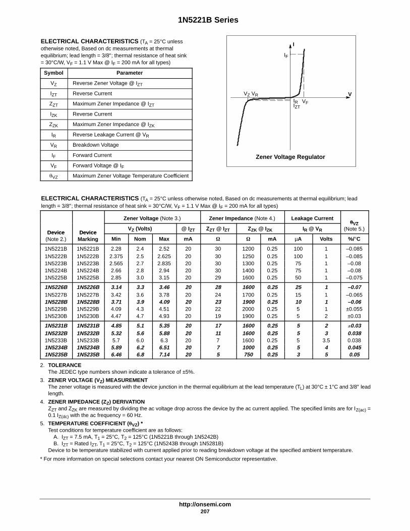
Zener Voltage Regulator
IF
V
I
IRIZT
VRVZ
VF
1N5221B Series
http://onsemi.com207
ELECTRICAL CHARACTERISTICS (TA = 25°C unlessotherwise noted, Based on dc measurements at thermalequilibrium; lead length = 3/8″; thermal resistance of heat sink= 30°C/W, VF = 1.1 V Max @ IF = 200 mA for all types)
Symbol Parameter
VZ Reverse Zener Voltage @ IZT
IZT Reverse Current
ZZT Maximum Zener Impedance @ IZT
IZK Reverse Current
ZZK Maximum Zener Impedance @ IZK
IR Reverse Leakage Current @ VR
VR Breakdown Voltage
IF Forward Current
VF Forward Voltage @ IF
VZ Maximum Zener Voltage Temperature Coefficient
ELECTRICAL CHARACTERISTICS (TA = 25°C unless otherwise noted, Based on dc measurements at thermal equilibrium; leadlength = 3/8″; thermal resistance of heat sink = 30°C/W, VF = 1.1 V Max @ IF = 200 mA for all types)
Zener Voltage (Note 3.) Zener Impedance (Note 4.) Leakage CurrentVZ
Device DeviceVZ (Volts) @ IZT ZZT @ IZT ZZK @ IZK IR @ VR
VZ(Note 5.)
Device(Note 2.)
DeviceMarking Min Nom Max mA mA µA Volts %/C
1N5221B 1N5221B 2.28 2.4 2.52 20 30 1200 0.25 100 1 –0.0851N5222B 1N5222B 2.375 2.5 2.625 20 30 1250 0.25 100 1 –0.0851N5223B 1N5223B 2.565 2.7 2.835 20 30 1300 0.25 75 1 –0.081N5224B 1N5224B 2.66 2.8 2.94 20 30 1400 0.25 75 1 –0.081N5225B 1N5225B 2.85 3.0 3.15 20 29 1600 0.25 50 1 –0.075
1N5226B 1N5226B 3.14 3.3 3.46 20 28 1600 0.25 25 1 –0.071N5227B 1N5227B 3.42 3.6 3.78 20 24 1700 0.25 15 1 –0.0651N5228B 1N5228B 3.71 3.9 4.09 20 23 1900 0.25 10 1 –0.061N5229B 1N5229B 4.09 4.3 4.51 20 22 2000 0.25 5 1 ±0.0551N5230B 1N5230B 4.47 4.7 4.93 20 19 1900 0.25 5 2 ±0.03
1N5231B 1N5231B 4.85 5.1 5.35 20 17 1600 0.25 5 2 0.031N5232B 1N5232B 5.32 5.6 5.88 20 11 1600 0.25 5 3 0.0381N5233B 1N5233B 5.7 6.0 6.3 20 7 1600 0.25 5 3.5 0.0381N5234B 1N5234B 5.89 6.2 6.51 20 7 1000 0.25 5 4 0.0451N5235B 1N5235B 6.46 6.8 7.14 20 5 750 0.25 3 5 0.05
2. TOLERANCEThe JEDEC type numbers shown indicate a tolerance of ±5%.
3. ZENER VOLTAGE (VZ) MEASUREMENTThe zener voltage is measured with the device junction in the thermal equilibrium at the lead temperature (TL) at 30°C ± 1°C and 3/8″ leadlength.
4. ZENER IMPEDANCE (ZZ) DERIVATIONZZT and ZZK are measured by dividing the ac voltage drop across the device by the ac current applied. The specified limits are for IZ(ac) =0.1 IZ(dc) with the ac frequency = 60 Hz.
5. TEMPERATURE COEFFICIENT (VZ) *Test conditions for temperature coefficient are as follows:
A. IZT = 7.5 mA, T1 = 25°C, T2 = 125°C (1N5221B through 1N5242B)B. IZT = Rated IZT, T1 = 25°C, T2 = 125°C (1N5243B through 1N5281B)
Device to be temperature stabilized with current applied prior to reading breakdown voltage at the specified ambient temperature.
* For more information on special selections contact your nearest ON Semiconductor representative.

1N5221B Series
http://onsemi.com208
ELECTRICAL CHARACTERISTICS (TA = 25°C unless otherwise noted, Based on dc measurements at thermal equilibrium; leadlength = 3/8″; thermal resistance of heat sink = 30°C/W, VF = 1.1 V Max @ IF = 200 mA for all types) (continued)
Zener Voltage (Note 7.) Zener Impedance (Note 8.) Leakage CurrentVZ
Device DeviceVZ (Volts) @ IZT ZZT @ IZT ZZK @ IZK IR @ VR
VZ(Note 9.)
Device(Note 6.)
DeviceMarking Min Nom Max mA mA µA Volts %/C
1N5236B 1N5236B 7.13 7.5 7.87 20 6 500 0.25 3 6 0.0581N5237B 1N5237B 7.79 8.2 8.61 20 8 500 0.25 3 6.5 0.0621N5238B 1N5238B 8.265 8.7 9.135 20 8 600 0.25 3 6.5 0.0651N5239B 1N5239B 8.65 9.1 9.55 20 10 600 0.25 3 7 0.0681N5240B 1N5240B 9.5 10 10.5 20 17 600 0.25 3 8 0.075
1N5241B 1N5241B 10.45 11 11.55 20 22 600 0.25 2 8.4 0.0761N5242B 1N5242B 11.4 12 12.6 20 30 600 0.25 1 9.1 0.0771N5243B 1N5243B 12.35 13 13.65 9.5 13 600 0.25 0.5 9.9 0.0791N5244B 1N5244B 13.3 14 14.7 9 15 600 0.25 0.1 10 0.0821N5245B 1N5245B 14.25 15 15.75 8.5 16 600 0.25 0.1 11 0.082
1N5246B 1N5246B 15.2 16 16.8 7.8 17 600 0.25 0.1 12 0.0831N5247B 1N5247B 16.15 17 17.85 7.4 19 600 0.25 0.1 13 0.0841N5248B 1N5248B 17.1 18 18.9 7 21 600 0.25 0.1 14 0.0851N5249B 1N5249B 18.05 19 19.95 6.6 23 600 0.25 0.1 14 0.0861N5250B 1N5250B 19 20 21 6.2 25 600 0.25 0.1 15 0.086
1N5251B 1N5251B 20.9 22 23.1 5.6 29 600 0.25 0.1 17 0.0871N5252B 1N5252B 22.8 24 25.2 5.2 33 600 0.25 0.1 18 0.0881N5253B 1N5253B 23.75 25 26.25 5.0 35 600 0.25 0.1 19 0.0891N5254B 1N5254B 25.65 27 28.35 4.6 41 600 0.25 0.1 21 0.0901N5255B 1N5255B 26.6 28 29.4 4.5 44 600 0.25 0.1 21 0.091
1N5256B 1N5256B 28.5 30 31.5 4.2 49 600 0.25 0.1 23 0.0911N5257B 1N5257B 31.35 33 34.65 3.8 58 700 0.25 0.1 25 0.0921N5258B 1N5258B 34.2 36 37.8 3.4 70 700 0.25 0.1 27 0.0931N5259B 1N5259B 37.05 39 40.95 3.2 80 800 0.25 0.1 30 0.0941N5260B 1N5260B 40.85 43 45.15 3.0 93 900 0.25 0.1 33 0.095
1N5261B 1N5261B 44.65 47 49.35 2.7 105 1000 0.25 0.1 36 0.0951N5262B 1N5262B 48.45 51 53.55 2.5 125 1100 0.25 0.1 39 0.0961N5263B 1N5263B 53.2 56 58.8 2.2 150 1300 0.25 0.1 43 0.0961N5264B 1N5264B 57 60 63 2.1 170 1400 0.25 0.1 46 0.0971N5265B 1N5265B 58.9 62 65.1 2.0 185 1400 0.25 0.1 47 0.097
1N5266B 1N5266B 64.6 68 71.4 1.8 230 1600 0.25 0.1 52 0.0971N5267B 1N5267B 71.25 75 78.75 1.7 270 1700 0.25 0.1 56 0.0981N5268B 1N5268B 77.9 82 86.1 1.5 330 2000 0.25 0.1 62 0.0981N5269B 1N5269B 82.65 87 91.35 1.4 370 2200 0.25 0.1 68 0.0991N5270B 1N5270B 86.45 91 95.55 1.4 400 2300 0.25 0.1 69 0.099
6. TOLERANCEThe JEDEC type numbers shown indicate a tolerance of ±5%.
7. ZENER VOLTAGE (VZ) MEASUREMENTThe zener voltage is measured with the device junction in the thermal equilibrium at the lead temperature (TL) at 30°C ± 1°C and 3/8″ leadlength.
8. ZENER IMPEDANCE (ZZ) DERIVATIONZZT and ZZK are measured by dividing the ac voltage drop across the device by the ac current applied. The specified limits are for IZ(ac) =0.1 IZ(dc) with the ac frequency = 60 Hz.
9. TEMPERATURE COEFFICIENT (VZ) *Test conditions for temperature coefficient are as follows:
A. IZT = 7.5 mA, T1 = 25°C, T2 = 125°C (1N5221B through 1N5242B)B. IZT = Rated IZT, T1 = 25°C, T2 = 125°C (1N5243B through 1N5281B)
Device to be temperature stabilized with current applied prior to reading breakdown voltage at the specified ambient temperature.
* For more information on special selections contact your nearest ON Semiconductor representative.

1N5221B Series
http://onsemi.com209
0.7
0.6
0.5
0.4
0.3
0.2
0.1
00 20 40 60 80 100 120 140 160 180 200
TL, LEAD TEMPERATURE (°C)
Figure 1. Steady State Power Derating
HEATSINKS
3/8" 3/8"
PD
, ST
EA
DY
STA
TE
PO
WE
R D
ISS
IPA
TIO
N (
WA
TT
S)

1N5221B Series
http://onsemi.com210
APPLICATION NOTE — ZENER VOLTAGE
Since the actual voltage available from a given zenerdiode is temperature dependent, it is necessary to determinejunction temperature under any set of operating conditionsin order to calculate its value. The following procedure isrecommended:
Lead Temperature, TL, should be determined from:
TL = θLAPD + TA.
θLA is the lead-to-ambient thermal resistance (°C/W) and PDis the power dissipation. The value for θLA will vary anddepends on the device mounting method. θLA is generally 30to 40°C/W for the various clips and tie points in common useand for printed circuit board wiring.
The temperature of the lead can also be measured using athermocouple placed on the lead as close as possible to thetie point. The thermal mass connected to the tie point isnormally large enough so that it will not significantlyrespond to heat surges generated in the diode as a result ofpulsed operation once steady-state conditions are achieved.Using the measured value of TL, the junction temperaturemay be determined by:
TJ = TL + ∆TJL.
∆TJL is the increase in junction temperature above the leadtemperature and may be found from Figure 2 for dc power:
∆TJL = θJLPD.
For worst-case design, using expected limits of IZ, limitsof PD and the extremes of TJ(∆TJ) may be estimated.Changes in voltage, VZ, can then be found from:
∆V = θVZTJ.
θVZ, the zener voltage temperature coefficient, is foundfrom Figures 4 and 5.
Under high power-pulse operation, the zener voltage willvary with time and may also be affected significantly by thezener resistance. For best regulation, keep currentexcursions as low as possible.
Surge limitations are given in Figure 7. They are lowerthan would be expected by considering only junctiontemperature, as current crowding effects cause temperaturesto be extremely high in small spots, resulting in devicedegradation should the limits of Figure 7 be exceeded.
L L
500
400
300
200
100
00 0.2 0.4 0.6 0.8 1
2.4-60V
62-200V
L, LEAD LENGTH TO HEAT SINK (INCH)JL, J
UN
CT
ION
TO
LE
AD
TH
ER
MA
L R
ES
ISTA
NC
E (
C/W
)θ
°
Figure 2. Typical Thermal Resistance
TYPICAL LEAKAGE CURRENTAT 80% OF NOMINALBREAKDOWN VOLTAGE
+25°C
+125°C
100070005000
2000
1000700500
200
1007050
20
1075
2
10.70.5
0.2
0.10.070.05
0.02
0.010.0070.005
0.002
0.0013 4 5 6 7 8 9 10 11 12 13 14 15
VZ, NOMINAL ZENER VOLTAGE (VOLTS)
I, L
EA
KA
GE
CU
RR
EN
T (
A)
µR
Figure 3. Typical Leakage Current

1N5221B Series
http://onsemi.com211
+12
+10
+8
+6
+4
+2
0
-2
-42 3 4 5 6 7 8 9 10 11 12
VZ, ZENER VOLTAGE (VOLTS)
Figure 4a. Range for Units to 12 Volts
VZ@IZT(NOTE 2)
RANGE
TEMPERATURE COEFFICIENTS(–55°C to +150°C temperature range; 90% of the units are in the ranges indicated.)
100
7050
30
20
10
7
5
3
2
12 3 4 5 6 7 8 9 10 11 12 10 20 30 50 70 100
VZ, ZENER VOLTAGE (VOLTS)
Figure 4b. Range for Units 12 to 100 Volts
RANGE VZ@IZ(NOTE 2)
120 130 140 150 160 170 180 190 200
200
180
160
140
120
100
VZ, ZENER VOLTAGE (VOLTS)
Figure 4c. Range for Units 120 to 200 Volts
VZ@IZT(NOTE 2)
+6
+4
+2
0
-2
-43 4 5 6 7 8
VZ, ZENER VOLTAGE (VOLTS)
Figure 5. Effect of Zener Current
NOTE: BELOW 3 VOLTS AND ABOVE 8 VOLTSNOTE: CHANGES IN ZENER CURRENT DO NOTNOTE: AFFECT TEMPERATURE COEFFICIENTS
1mA
0.01mA
VZ@IZTA=25°C
1000
C, C
APA
CIT
AN
CE
(pF
)
500
200
100
50
20
10
5
2
11 2 5 10 20 50 100
VZ, ZENER VOLTAGE (VOLTS)
Figure 6a. Typical Capacitance 2.4–100 Volts
TA=25°C
0V BIAS
1V BIAS
50% OFVZBIAS
10070
50
30
20
10
75
3
2
1120 140 160 180 190 200 220
VZ, ZENER VOLTAGE (VOLTS)
Figure 6b. Typical Capacitance 120–200 Volts
TA=25°C
1VOLTBIAS
50% OF VZBIAS
0 BIAS
θVZ
, TE
MP
ER
ATU
RE
CO
EF
FIC
IEN
T (m
V/°
C)
20mA
C, C
APA
CIT
AN
CE
(pF
)θV
Z, T
EM
PE
RAT
UR
E C
OE
FF
ICIE
NT
(mV
/°C
)θV
Z, T
EM
PE
RAT
UR
E C
OE
FF
ICIE
NT
(mV
/°C
)
θVZ
, TE
MP
ER
ATU
RE
CO
EF
FIC
IEN
T (m
V/°
C)

1N5221B Series
http://onsemi.com212
100
7050
30
20
10
7
5
3
2
10.01 0.02 0.05 0.1 0.2 0.5 1 2 5 10 20 50 100 200 500 1000
P pk
, PE
AK
SU
RG
E P
OW
ER
(W
AT
TS
)
PW, PULSE WIDTH (ms)
5% DUTY CYCLE
10% DUTY CYCLE
20% DUTY CYCLE
11V-91V NONREPETITIVE
1.8V-10V NONREPETITIVE
RECTANGULARWAVEFORMTJ=25°C PRIOR TOINITIAL PULSE
Figure 7a. Maximum Surge Power 1.8–91 Volts
1000700500
300200
1007050
3020
107532
10.01 0.1 1 10 100 1000
P pk
, PE
AK
SU
RG
E P
OW
ER
(W
AT
TS
)
PW, PULSE WIDTH (ms)
Figure 7b. Maximum Surge Power DO-204AH100–200 Volts
1000500
200
100
50
20
10
1
2
5
0.1 0.2 0.5 1 2 5 10 20 50 100
IZ, ZENER CURRENT (mA)
Figure 8. Effect of Zener Current onZener Impedance
Z Z, D
YN
AM
IC IM
PE
DA
NC
E (
OH
MS
)
Z Z, D
YN
AM
IC IM
PE
DA
NC
E (
OH
MS
)
1000700500
200
1007050
20
1075
2
11 2 3 5 7 10 20 30 50 70 100
VZ, ZENER VOLTAGE (VOLTS)
Figure 9. Effect of Zener Voltage on Zener Impedance Figure 10. Typical Forward Characteristics
RECTANGULARWAVEFORM, TJ=25°C
100-200VOLTS NONREPETITIVE
TJ=25°C
iZ(rms)=0.1 IZ(dc)
f=60HzIZ=1mA
5mA
20mA
TJ=25°C
iZ(rms)=0.1 IZ(dc)
f=60Hz
VZ=2.7V
47V
27V
6.2V
VF, FORWARD VOLTAGE (VOLTS)
0.4 0.5 0.6 0.7 0.8 0.9 1 1.1
1000
500
200
100
50
20
10
5
2
1
I F, F
OR
WA
RD
CU
RR
EN
T (m
A) MINIMUM
MAXIMUM
150°C
75°C
0°C
25°C

1N5221B Series
http://onsemi.com213
Figure 11. Zener Voltage versus Zener Current — V Z = 1 thru 16 Volts
VZ, ZENER VOLTAGE (VOLTS)
I Z, Z
EN
ER
CU
RR
EN
T (m
A)
20
10
1
0.1
0.011 2 3 4 5 6 7 8 9 10 11 12 13 14 15 16
TA=25°
Figure 12. Zener Voltage versus Zener Current — V Z = 15 thru 30 Volts
VZ, ZENER VOLTAGE (VOLTS)
15 16 17 18 19 20 21 22 23 24 25 26 27 28 29 30
10
1
0.1
0.01
TA=25°
I Z, Z
EN
ER
CU
RR
EN
T (m
A)
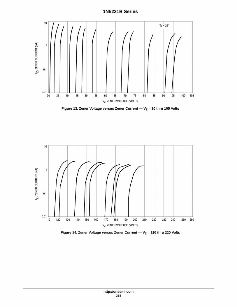
1N5221B Series
http://onsemi.com214
Figure 13. Zener Voltage versus Zener Current — V Z = 30 thru 105 Volts
VZ, ZENER VOLTAGE (VOLTS)
10
1
0.1
0.0130 35 40 45 50 55 60 70 75 80 85 90 95 100
Figure 14. Zener Voltage versus Zener Current — V Z = 110 thru 220 Volts
VZ, ZENER VOLTAGE (VOLTS)
110 120 130 140 150 160 170 180 190 200 210 220 230 240 250 260
10
1
0.1
0.01
TA=25°
65 105
I Z, Z
EN
ER
CU
RR
EN
T (m
A)
I Z, Z
EN
ER
CU
RR
EN
T (m
A)

Semiconductor Components Industries, LLC, 2000
November, 2000 – Rev. 1215 Publication Order Number:
1N4728A/D
1N4728A Series
1 Watt DO-41 HermeticallySealed Glass Zener VoltageRegulator Diodes
This is a complete series of 1 Watt Zener diode with limits andexcellent operating characteristics that reflect the superior capabilitiesof silicon–oxide passivated junctions. All this in an axial–leadhermetically sealed glass package that offers protection in all commonenvironmental conditions.
Specification Features:• Zener Voltage Range – 3.3 V to 91 V
• ESD Rating of Class 3 (>16 KV) per Human Body Model
• DO–41 (DO–204AL) Package
• Double Slug Type Construction
• Metallurgical Bonded Construction
• Oxide Passivated Die
Mechanical Characteristics:CASE: Double slug type, hermetically sealed glassFINISH: All external surfaces are corrosion resistant and leads arereadily solderableMAXIMUM LEAD TEMPERATURE FOR SOLDERING PURPOSES:230°C, 1/16″ from the case for 10 secondsPOLARITY: Cathode indicated by polarity bandMOUNTING POSITION: Any
MAXIMUM RATINGS
Rating Symbol Value Unit
Max. Steady State Power Dissipation@ TL ≤ 50°C, Lead Length = 3/8″Derated above 50°C
PD 1.0
6.67
Watt
mW/°C
Operating and StorageTemperature Range
TJ, Tstg – 65 to+200
°C
Devices listed in bold, italic are ON SemiconductorPreferred devices. Preferred devices are recommendedchoices for future use and best overall value.
Device Package Shipping
ORDERING INFORMATION (1.)(NO TAG)
1N47xxA Axial Lead 2000 Units/Box
1N47xxARL Axial Lead
AXIAL LEADCASE 59GLASS
http://onsemi.com
6000/Tape & Reel
Cathode Anode
1N47xxARL2 Axial Lead 6000/Tape & Reel
1N47xxATA Axial Lead 4000/Ammo Pack
1N47xxATA2 Axial Lead 4000/Ammo Pack
1. The “2” suffix refers to 26 mm tape spacing.NOTES:
L1N47xxAYWW
L = Assembly Location1N47xxA= Device CodeY = YearWW = Work Week

Zener Voltage Regulator
IF
V
I
IRIZT
VRVZ
VF
1N4728A Series
http://onsemi.com216
ELECTRICAL CHARACTERISTICS (TA = 25°C unlessotherwise noted, VF = 1.2 V Max., IF = 200 mA for all types)
Symbol Parameter
VZ Reverse Zener Voltage @ IZT
IZT Reverse Current
ZZT Maximum Zener Impedance @ IZT
IZK Reverse Current
ZZK Maximum Zener Impedance @ IZK
IR Reverse Leakage Current @ VR
VR Breakdown Voltage
IF Forward Current
VF Forward Voltage @ IF
Ir Surge Current @ TA = 25°C
ELECTRICAL CHARACTERISTICS (TA = 25°C unless otherwise noted, VF = 1.2 V Max, IF = 200 mA for all types)
Zener Voltage (3.)(4.) Zener Impedance (5.) Leakage Current
JEDECVZ (Volts) @ IZT ZZT @ IZT ZZK @ IZK IR @ VR Ir (6.)
JEDECDevice (2.) Min Nom Max (mA) () () (mA) (µA Max) (Volts) (mA)
1N4728A 3.14 3.3 3.47 76 10 400 1 100 1 13801N4729A 3.42 3.6 3.78 69 10 400 1 100 1 12601N4730A 3.71 3.9 4.10 64 9 400 1 50 1 11901N4731A 4.09 4.3 4.52 58 9 400 1 10 1 10701N4732A 4.47 4.7 4.94 53 8 500 1 10 1 970
1N4733A 4.85 5.1 5.36 49 7 550 1 10 1 8901N4734A 5.32 5.6 5.88 45 5 600 1 10 2 8101N4735A 5.89 6.2 6.51 41 2 700 1 10 3 7301N4736A 6.46 6.8 7.14 37 3.5 700 1 10 4 6601N4737A 7.13 7.5 7.88 34 4 700 0.5 10 5 605
1N4738A 7.79 8.2 8.61 31 4.5 700 0.5 10 6 5501N4739A 8.65 9.1 9.56 28 5 700 0.5 10 7 5001N4740A 9.50 10 10.50 25 7 700 0.25 10 7.6 4541N4741A 10.45 11 11.55 23 8 700 0.25 5 8.4 4141N4742A 11.40 12 12.60 21 9 700 0.25 5 9.1 380
1N4743A 12.4 13 13.7 19 10 700 0.25 5 9.9 3441N4744A 14.3 15 15.8 17 14 700 0.25 5 11.4 3041N4745A 15.2 16 16.8 15.5 16 700 0.25 5 12.2 285
TOLERANCE AND TYPE NUMBER DESIGNATION2. The JEDEC type numbers listed have a standard tolerance on the nominal zener voltage of ±5%.
SPECIALS AVAILABLE INCLUDE:3. Nominal zener voltages between the voltages shown and tighter voltage tolerances. For detailed information on price, availability, and
delivery, contact your nearest ON Semiconductor representative.
ZENER VOLTAGE (VZ) MEASUREMENT4. ON Semiconductor guarantees the zener voltage when measured at 90 seconds while maintaining the lead temperature (TL) at 30°C
± 1°C, 3/8″ from the diode body.
ZENER IMPEDANCE (ZZ) DERIVATION5. The zener impedance is derived from the 60 cycle ac voltage, which results when an ac current having an rms value equal to 10% of the
dc zener current (IZT or IZK) is superimposed on IZT or IZK.
SURGE CURRENT (IR) NON-REPETITIVE6. The rating listed in the electrical characteristics table is maximum peak, non-repetitive, reverse surge current of 1/2 square wave or equiv-
alent sine wave pulse of 1/120 second duration superimposed on the test current, IZT, per JEDEC registration; however, actual devicecapability is as described in Figure 5 of the General Data – DO-41 Glass.

1N4728A Series
http://onsemi.com217
ELECTRICAL CHARACTERISTICS (TA = 25°C unless otherwise noted, VF = 1.2 V Max, IF = 200 mA for all types) (continued)
Zener Voltage (8.)(9.) Zener Impedance (10.) Leakage Current
JEDECVZ (Volts) @ IZT ZZT @ IZT ZZK @ IZK IR @ VR Ir (11.)
JEDECDevice (7.) Min Nom Max (mA) () () (mA) (µA Max) (Volts) (mA)
1N4746A 17.1 18 18.9 14 20 750 0.25 5 13.7 2501N4747A 19.0 20 21.0 12.5 22 750 0.25 5 15.2 225
1N4748A 20.9 22 23.1 11.5 23 750 0.25 5 16.7 2051N4749A 22.8 24 25.2 10.5 25 750 0.25 5 18.2 1901N4750A 25.7 27 28.4 9.5 35 750 0.25 5 20.6 1701N4751A 28.5 30 31.5 8.5 40 1000 0.25 5 22.8 1501N4752A 31.4 33 34.7 7.5 45 1000 0.25 5 25.1 135
1N4753A 34.2 36 37.8 7 50 1000 0.25 5 27.4 1251N4754A 37.1 39 41.0 6.5 60 1000 0.25 5 29.7 1151N4755A 40.9 43 45.2 6 70 1500 0.25 5 32.7 1101N4756A 44.7 47 49.4 5.5 80 1500 0.25 5 35.8 951N4757A 48.5 51 53.6 5 95 1500 0.25 5 38.8 90
1N4758A 53.2 56 58.8 4.5 110 2000 0.25 5 42.6 801N4759A 58.9 62 65.1 4 125 2000 0.25 5 47.1 701N4760A 64.6 68 71.4 3.7 150 2000 0.25 5 51.7 651N4761A 71.3 75 78.8 3.3 175 2000 0.25 5 56 601N4762A 77.9 82 86.1 3 200 3000 0.25 5 62.2 55
1N4763A 86.5 91 95.6 2.8 250 3000 0.25 5 69.2 50
TOLERANCE AND TYPE NUMBER DESIGNATION7. The JEDEC type numbers listed have a standard tolerance on the nominal zener voltage of ±5%.SPECIALS AVAILABLE INCLUDE:8. Nominal zener voltages between the voltages shown and tighter voltage tolerances. For detailed information on price, availability, and
delivery, contact your nearest ON Semiconductor representative.ZENER VOLTAGE (VZ) MEASUREMENT9. ON Semiconductor guarantees the zener voltage when measured at 90 seconds while maintaining the lead temperature (TL) at 30°C ± 1°C,
3/8″ from the diode body.ZENER IMPEDANCE (ZZ) DERIVATION10.The zener impedance is derived from the 60 cycle ac voltage, which results when an ac current having an rms value equal to 10% of the
dc zener current (IZT or IZK) is superimposed on IZT or IZK.SURGE CURRENT (IR) NON-REPETITIVE11. The rating listed in the electrical characteristics table is maximum peak, non-repetitive, reverse surge current of 1/2 square wave or equivalent
sine wave pulse of 1/120 second duration superimposed on the test current, IZT, per JEDEC registration; however, actual device capabilityis as described in Figure 5 of the General Data – DO-41 Glass.
Figure 1. Power Temperature Derating Curve
TL, LEAD TEMPERATURE (°C)
P D
0 20 40 60 20080 100 120 140 160 180
0.25
0.5
0.75
1
1.25L = LEAD LENGTH TO HEAT SINK
L = 3/8″L = 1/8″L = 1″
, MA
XIM
UM
ST
EA
DY
STA
TE
PO
WE
R D
ISS
IPA
TIO
N (
WA
TT
S)

1N4728A Series
http://onsemi.com218
Figure 2. Temperature Coefficients(–55°C to +150°C temperature range; 90% of the units are in the ranges indicated.)
a. Range for Units to 12 Volts b. Range for Units to 12 to 100 Volts
+12
+10
+8
+6
+4
+2
0
-2
-42 3 4 5 6 7 8 9 10 11 12
VZ, ZENER VOLTAGE (VOLTS)
θVZ
, TE
MP
ER
ATU
RE
CO
EF
FIC
IEN
T (m
V/°
C)
100
70
50
30
20
10
75
3
2
110 20 30 50 70 100
VZ, ZENER VOLTAGE (VOLTS)
θVZ
, TE
MP
ER
ATU
RE
CO
EF
FIC
IEN
T (m
V/°
C)
VZ@IZTRANGE
RANGE VZ@IZT
Figure 3. Typical Thermal Resistanceversus Lead Length
Figure 4. Effect of Zener Current
175
150
125
100
75
50
25
00 0.1 0.2 0.3 0.4 0.5 0.6 0.7 0.8 0.9 1
L, LEAD LENGTH TO HEAT SINK (INCHES)θ JL
, JU
NC
TIO
NT
OL
EA
D T
HE
RM
AL
RE
SIS
TAN
CE
(m
V/ °
C/W
)
θVZ
, TE
MP
ER
ATU
RE
CO
EF
FIC
IEN
T (m
V/°
C) +6
+4
+2
0
-2
-43 4 5 6 7 8
VZ, ZENER VOLTAGE (VOLTS)
VZ@IZTA=25°C
20mA
0.01mA
1mA
NOTE: BELOW 3 VOLTS AND ABOVE 8 VOLTSNOTE: CHANGES IN ZENER CURRENT DO NOTNOTE: EFFECT TEMPERATURE COEFFICIENTS
Figure 5. Maximum Surge Power
100
7050
30
20
10
7
5
3
2
10.01 0.02 0.05 0.1 0.2 0.5 1 2 5 10 20 50 100 200 500 1000
PW, PULSE WIDTH (ms)This graph represents 90 percentile data points.For worst case design characteristics, multiply surge power by 2/3.
Ppk
, PE
AK
SU
RG
E P
OW
ER
(W
AT
TS
)
11V-100V NONREPETITIVE
3.3V-10V NONREPETITIVE5% DUTY CYCLE
10% DUTY CYCLE
20% DUTY CYCLE
RECTANGULARWAVEFORMTJ=25°C PRIOR TOINITIAL PULSE

1N4728A Series
http://onsemi.com219
VF, FORWARD VOLTAGE (VOLTS)
0.4 0.5 0.6 0.7 0.8 0.9 1 1.1
1000
500
200
100
50
20
10
5
2
1
I F, F
OR
WA
RD
CU
RR
EN
T (m
A) MAXIMUM
150°C
75°C
0°C
25°C
Figure 6. Effect of Zener Currenton Zener Impedance
Figure 7. Effect of Zener Voltageon Zener Impedance
Figure 8. Typical Leakage Current
1000500
200
100
50
20
10
5
2
10.1 0.2 0.5 1 2 5 10 20 50 100
IZ, ZENER CURRENT (mA)
ZZ
, DY
NA
MIC
IMP
ED
AN
CE
(O
HM
S)
1000700500
200
1007050
20
1075
2
11 2 100
VZ, ZENER VOLTAGE (V)
3 5 7 10 20 30 50 70
ZZ
, DY
NA
MIC
IMP
ED
AN
CE
(O
HM
S)
1000070005000
2000
1000700500
200
1007050
20
1075
2
10.70.5
0.2
0.10.070.05
0.02
0.010.0070.005
0.002
0.001
I R, L
EA
KA
GE
CU
RR
EN
T (µ
A)
3 4 5 6 7 8 9 10 11 12 13 14 15
VZ, NOMINAL ZENER VOLTAGE (VOLTS)
+25°C
+125°C
TYPICAL LEAKAGE CURRENT
AT 80% OF NOMINAL
BREAKDOWN VOLTAGE
TJ = 25°CiZ(rms) = 0.1 IZ(dc)f = 60 Hz
6.2 V
27 V
VZ = 2.7 V
47 V
TJ = 25°CiZ(rms) = 0.1 IZ(dc)f = 60 Hz
20 mA
5 mA
IZ = 1 mA
0 V BIAS
1 V BIAS
400300
200
100
50
20
108
41 2 5 10 20 50 100
VZ, NOMINAL VZ (VOLTS)
C, C
APA
CIT
AN
CE
(pF
)
50% OF BREAKDOWN BIAS
MINIMUM
Figure 9. Typical Capacitance versus V Z
Figure 10. Typical Forward Characteristics

1N4728A Series
http://onsemi.com220
APPLICATION NOTE
Since the actual voltage available from a given zenerdiode is temperature dependent, it is necessary to determinejunction temperature under any set of operating conditionsin order to calculate its value. The following procedure isrecommended:
Lead Temperature, TL, should be determined from:
TL = θLAPD + TA.
θLA is the lead-to-ambient thermal resistance (°C/W) and PDis the power dissipation. The value for θLA will vary anddepends on the device mounting method. θLA is generally 30to 40°C/W for the various clips and tie points in common useand for printed circuit board wiring.
The temperature of the lead can also be measured using athermocouple placed on the lead as close as possible to thetie point. The thermal mass connected to the tie point isnormally large enough so that it will not significantlyrespond to heat surges generated in the diode as a result ofpulsed operation once steady-state conditions are achieved.Using the measured value of TL, the junction temperaturemay be determined by:
TJ = TL + ∆TJL.
∆TJL is the increase in junction temperature above the leadtemperature and may be found as follows:
∆TJL = θJLPD.
θJL may be determined from Figure 3 for dc powerconditions. For worst-case design, using expected limits ofIZ, limits of PD and the extremes of TJ(∆TJ) may beestimated. Changes in voltage, VZ, can then be found from:
∆V = θVZ ∆TJ.
θVZ, the zener voltage temperature coefficient, is foundfrom Figure 2.
Under high power-pulse operation, the zener voltage willvary with time and may also be affected significantly by thezener resistance. For best regulation, keep currentexcursions as low as possible.
Surge limitations are given in Figure 5. They are lowerthan would be expected by considering only junctiontemperature, as current crowding effects cause temperaturesto be extremely high in small spots, resulting in devicedegradation should the limits of Figure 5 be exceeded.

Semiconductor Components Industries, LLC, 2001
May, 2001 – Rev. 0221 Publication Order Number:
BZX85C3V3RL/D
BZX85C3V3RL Series
1 Watt DO-41 HermeticallySealed Glass Zener VoltageRegulators
This is a complete series of 1 Watt Zener diodes with limits andexcellent operating characteristics that reflect the superior capabilitiesof silicon–oxide passivated junctions. All this in an axial–leadhermetically sealed glass package that offers protection in all commonenvironmental conditions.
Specification Features:• Zener Voltage Range – 3.3 V to 85 V
• ESD Rating of Class 3 (>16 KV) per Human Body Model
• DO–41 (DO–204AL) Package
• Double Slug Type Construction
• Metallurgical Bonded Construction
• Oxide Passivated Die
Mechanical Characteristics:CASE: Double slug type, hermetically sealed glassFINISH: All external surfaces are corrosion resistant and leads arereadily solderableMAXIMUM LEAD TEMPERATURE FOR SOLDERING PURPOSES:230°C, 1/16″ from the case for 10 secondsPOLARITY: Cathode indicated by polarity bandMOUNTING POSITION: Any
MAXIMUM RATINGS
Rating Symbol Value Unit
Max. Steady State Power Dissipation@ TL ≤ 50°C, Lead Length = 3/8″Derate above 50°C
PD 1
6.67
W
mW/°C
Operating and StorageTemperature Range
TJ, Tstg –65 to+200
°CDevice Package Shipping
ORDERING INFORMATION
BZX85CxxxRL Axial Lead 6000/Tape & Reel
BZX85CxxxRL2 Axial Lead
AXIAL LEADCASE 59GLASS
http://onsemi.com
6000/Tape & Reel
Cathode Anode
* The “2” suffix refers to 26 mm tape spacing.
LBZX85CxxxYWW
L = Assembly LocationBZX85Cxxx= Device Code
= (See Table Next Page)Y = YearWW = Work Week
MARKING DIAGRAM

Zener Voltage Regulator
IF
V
I
IRIZT
VRVZ
VF
BZX85C3V3RL Series
http://onsemi.com222
ELECTRICAL CHARACTERISTICS (TA = 25°C unlessotherwise noted, VF = 1.2 V Max., IF = 200 mA for all types)
Symbol Parameter
VZ Reverse Zener Voltage @ IZT
IZT Reverse Current
ZZT Maximum Zener Impedance @ IZT
IZK Reverse Current
ZZK Maximum Zener Impedance @ IZK
IR Reverse Leakage Current @ VR
VR Breakdown Voltage
IF Forward Current
VF Forward Voltage @ IF
IR Surge Current @ TA = 25°C
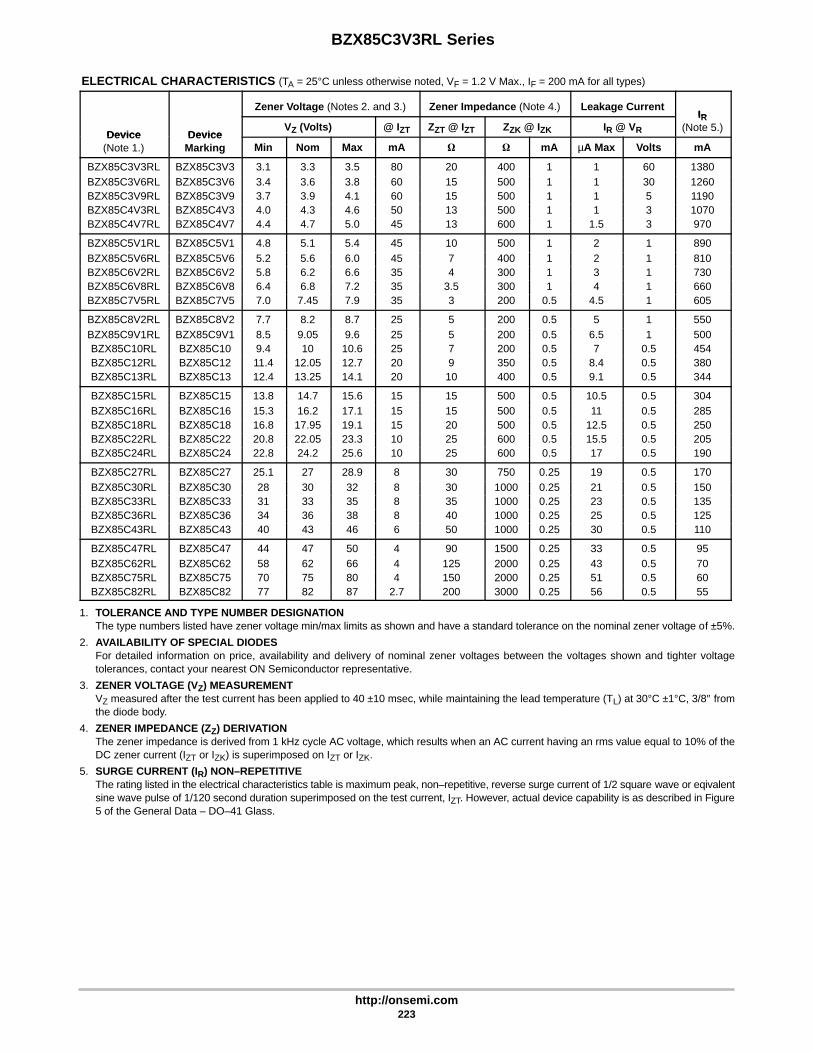
BZX85C3V3RL Series
http://onsemi.com223
ELECTRICAL CHARACTERISTICS (TA = 25°C unless otherwise noted, VF = 1.2 V Max., IF = 200 mA for all types)
Zener Voltage (Notes 2. and 3.) Zener Impedance (Note 4.) Leakage CurrentIR
Device DeviceVZ (Volts) @ IZT ZZT @ IZT ZZK @ IZK IR @ VR
IR(Note 5.)
Device(Note 1.)
DeviceMarking Min Nom Max mA mA µA Max Volts mA
BZX85C3V3RL BZX85C3V3 3.1 3.3 3.5 80 20 400 1 1 60 1380BZX85C3V6RL BZX85C3V6 3.4 3.6 3.8 60 15 500 1 1 30 1260BZX85C3V9RL BZX85C3V9 3.7 3.9 4.1 60 15 500 1 1 5 1190BZX85C4V3RL BZX85C4V3 4.0 4.3 4.6 50 13 500 1 1 3 1070BZX85C4V7RL BZX85C4V7 4.4 4.7 5.0 45 13 600 1 1.5 3 970
BZX85C5V1RL BZX85C5V1 4.8 5.1 5.4 45 10 500 1 2 1 890BZX85C5V6RL BZX85C5V6 5.2 5.6 6.0 45 7 400 1 2 1 810BZX85C6V2RL BZX85C6V2 5.8 6.2 6.6 35 4 300 1 3 1 730BZX85C6V8RL BZX85C6V8 6.4 6.8 7.2 35 3.5 300 1 4 1 660BZX85C7V5RL BZX85C7V5 7.0 7.45 7.9 35 3 200 0.5 4.5 1 605
BZX85C8V2RL BZX85C8V2 7.7 8.2 8.7 25 5 200 0.5 5 1 550BZX85C9V1RL BZX85C9V1 8.5 9.05 9.6 25 5 200 0.5 6.5 1 500BZX85C10RL BZX85C10 9.4 10 10.6 25 7 200 0.5 7 0.5 454BZX85C12RL BZX85C12 11.4 12.05 12.7 20 9 350 0.5 8.4 0.5 380BZX85C13RL BZX85C13 12.4 13.25 14.1 20 10 400 0.5 9.1 0.5 344
BZX85C15RL BZX85C15 13.8 14.7 15.6 15 15 500 0.5 10.5 0.5 304BZX85C16RL BZX85C16 15.3 16.2 17.1 15 15 500 0.5 11 0.5 285BZX85C18RL BZX85C18 16.8 17.95 19.1 15 20 500 0.5 12.5 0.5 250BZX85C22RL BZX85C22 20.8 22.05 23.3 10 25 600 0.5 15.5 0.5 205BZX85C24RL BZX85C24 22.8 24.2 25.6 10 25 600 0.5 17 0.5 190
BZX85C27RL BZX85C27 25.1 27 28.9 8 30 750 0.25 19 0.5 170BZX85C30RL BZX85C30 28 30 32 8 30 1000 0.25 21 0.5 150BZX85C33RL BZX85C33 31 33 35 8 35 1000 0.25 23 0.5 135BZX85C36RL BZX85C36 34 36 38 8 40 1000 0.25 25 0.5 125BZX85C43RL BZX85C43 40 43 46 6 50 1000 0.25 30 0.5 110
BZX85C47RL BZX85C47 44 47 50 4 90 1500 0.25 33 0.5 95BZX85C62RL BZX85C62 58 62 66 4 125 2000 0.25 43 0.5 70BZX85C75RL BZX85C75 70 75 80 4 150 2000 0.25 51 0.5 60BZX85C82RL BZX85C82 77 82 87 2.7 200 3000 0.25 56 0.5 55
1. TOLERANCE AND TYPE NUMBER DESIGNATIONThe type numbers listed have zener voltage min/max limits as shown and have a standard tolerance on the nominal zener voltage of ±5%.
2. AVAILABILITY OF SPECIAL DIODESFor detailed information on price, availability and delivery of nominal zener voltages between the voltages shown and tighter voltagetolerances, contact your nearest ON Semiconductor representative.
3. ZENER VOLTAGE (VZ) MEASUREMENTVZ measured after the test current has been applied to 40 ±10 msec, while maintaining the lead temperature (TL) at 30°C ±1°C, 3/8″ fromthe diode body.
4. ZENER IMPEDANCE (ZZ) DERIVATIONThe zener impedance is derived from 1 kHz cycle AC voltage, which results when an AC current having an rms value equal to 10% of theDC zener current (IZT or IZK) is superimposed on IZT or IZK.
5. SURGE CURRENT (IR) NON–REPETITIVEThe rating listed in the electrical characteristics table is maximum peak, non–repetitive, reverse surge current of 1/2 square wave or eqivalentsine wave pulse of 1/120 second duration superimposed on the test current, IZT. However, actual device capability is as described in Figure5 of the General Data – DO–41 Glass.

BZX85C3V3RL Series
http://onsemi.com224
Figure 1. Power Temperature Derating Curve
TL, LEAD TEMPERATURE (°C)
0 20 40 60 20080 100 120 140 160 180
0.25
0.5
0.75
1
1.25L = LEAD LENGTH TO HEAT SINK
L = 3/8″L = 1/8″L = 1″
PD
, ST
EA
DY
STA
TE
PO
WE
R D
ISS
IPA
TIO
N (
WA
TT
S)

BZX85C3V3RL Series
http://onsemi.com225
Figure 2. Temperature Coefficients(–55°C to +150°C temperature range; 90% of the units are in the ranges indicated.)
a. Range for Units to 12 Volts b. Range for Units to 12 to 100 Volts
+12
+10
+8
+6
+4
+2
0
-2
-42 3 4 5 6 7 8 9 10 11 12
VZ, ZENER VOLTAGE (VOLTS)
θVZ
, TE
MP
ER
ATU
RE
CO
EF
FIC
IEN
T (m
V/°
C)
100
70
50
30
20
10
75
3
2
110 20 30 50 70 100
VZ, ZENER VOLTAGE (VOLTS)
θVZ
, TE
MP
ER
ATU
RE
CO
EF
FIC
IEN
T (m
V/°
C)
VZ@IZTRANGE
RANGE VZ@IZT
Figure 3. Typical Thermal Resistanceversus Lead Length
Figure 4. Effect of Zener Current
175
150
125
100
75
50
25
00 0.1 0.2 0.3 0.4 0.5 0.6 0.7 0.8 0.9 1
L, LEAD LENGTH TO HEAT SINK (INCHES)θ JL
, JU
NC
TIO
NT
OL
EA
D T
HE
RM
AL
RE
SIS
TAN
CE
(m
V/ °
C/W
)
θVZ
, TE
MP
ER
ATU
RE
CO
EF
FIC
IEN
T (m
V/°
C) +6
+4
+2
0
-2
-43 4 5 6 7 8
VZ, ZENER VOLTAGE (VOLTS)
VZ@IZTA=25°C
20mA
0.01mA
1mA
NOTE: BELOW 3 VOLTS AND ABOVE 8 VOLTSNOTE: CHANGES IN ZENER CURRENT DO NOTNOTE: EFFECT TEMPERATURE COEFFICIENTS
Figure 5. Maximum Surge Power
100
7050
30
20
10
7
5
3
2
10.01 0.02 0.05 0.1 0.2 0.5 1 2 5 10 20 50 100 200 500 1000
PW, PULSE WIDTH (ms)This graph represents 90 percentile data points.For worst case design characteristics, multiply surge power by 2/3.
Ppk
, PE
AK
SU
RG
E P
OW
ER
(W
AT
TS
)
11V-100V NONREPETITIVE
3.3V-10V NONREPETITIVE5% DUTY CYCLE
10% DUTY CYCLE
20% DUTY CYCLE
RECTANGULARWAVEFORMTJ=25°C PRIOR TOINITIAL PULSE

BZX85C3V3RL Series
http://onsemi.com226
VF, FORWARD VOLTAGE (VOLTS)
0.4 0.5 0.6 0.7 0.8 0.9 1 1.1
1000
500
200
100
50
20
10
5
2
1
I F, F
OR
WA
RD
CU
RR
EN
T (m
A) MAXIMUM
150°C
75°C
0°C
25°C
Figure 6. Effect of Zener Currenton Zener Impedance
Figure 7. Effect of Zener Voltageon Zener Impedance
Figure 8. Typical Leakage Current
1000500
200
100
50
20
10
5
2
10.1 0.2 0.5 1 2 5 10 20 50 100
IZ, ZENER CURRENT (mA)
ZZ
, DY
NA
MIC
IMP
ED
AN
CE
(O
HM
S)
1000700500
200
1007050
20
1075
2
11 2 100
VZ, ZENER VOLTAGE (V)
3 5 7 10 20 30 50 70
ZZ
, DY
NA
MIC
IMP
ED
AN
CE
(O
HM
S)
1000070005000
2000
1000700500
200
1007050
20
1075
2
10.70.5
0.2
0.10.070.05
0.02
0.010.0070.005
0.002
0.001
I R, L
EA
KA
GE
CU
RR
EN
T (µ
A)
3 4 5 6 7 8 9 10 11 12 13 14 15
VZ, NOMINAL ZENER VOLTAGE (VOLTS)
+25°C
+125°C
TYPICAL LEAKAGE CURRENT
AT 80% OF NOMINAL
BREAKDOWN VOLTAGE
TJ = 25°CiZ(rms) = 0.1 IZ(dc)f = 60 Hz
6.2 V
27 V
VZ = 2.7 V
47 V
TJ = 25°CiZ(rms) = 0.1 IZ(dc)f = 60 Hz
20 mA
5 mA
IZ = 1 mA
0 V BIAS
1 V BIAS
400300
200
100
50
20
108
41 2 5 10 20 50 100
VZ, NOMINAL VZ (VOLTS)
C, C
APA
CIT
AN
CE
(pF
)
50% OF BREAKDOWN BIAS
MINIMUM
Figure 9. Typical Capacitance versus V Z
Figure 10. Typical Forward Characteristics

BZX85C3V3RL Series
http://onsemi.com227
APPLICATION NOTE
Since the actual voltage available from a given zenerdiode is temperature dependent, it is necessary to determinejunction temperature under any set of operating conditionsin order to calculate its value. The following procedure isrecommended:
Lead Temperature, TL, should be determined from:
TL = θLAPD + TA.
θLA is the lead-to-ambient thermal resistance (°C/W) and PDis the power dissipation. The value for θLA will vary anddepends on the device mounting method. θLA is generally 30to 40°C/W for the various clips and tie points in common useand for printed circuit board wiring.
The temperature of the lead can also be measured using athermocouple placed on the lead as close as possible to thetie point. The thermal mass connected to the tie point isnormally large enough so that it will not significantlyrespond to heat surges generated in the diode as a result ofpulsed operation once steady-state conditions are achieved.Using the measured value of TL, the junction temperaturemay be determined by:
TJ = TL + ∆TJL.
∆TJL is the increase in junction temperature above the leadtemperature and may be found as follows:
∆TJL = θJLPD.
θJL may be determined from Figure 3 for dc powerconditions. For worst-case design, using expected limits ofIZ, limits of PD and the extremes of TJ(∆TJ) may beestimated. Changes in voltage, VZ, can then be found from:
∆V = θVZ ∆TJ.
θVZ, the zener voltage temperature coefficient, is foundfrom Figure 2.
Under high power-pulse operation, the zener voltage willvary with time and may also be affected significantly by thezener resistance. For best regulation, keep currentexcursions as low as possible.
Surge limitations are given in Figure 5. They are lowerthan would be expected by considering only junctiontemperature, as current crowding effects cause temperaturesto be extremely high in small spots, resulting in devicedegradation should the limits of Figure 5 be exceeded.

Semiconductor Components Industries, LLC, 2001
May, 2001 – Rev. 1228 Publication Order Number:
1N5913B/D
1N5913B Series
3 Watt DO-41 Surmetic 30Zener Voltage Regulators
This is a complete series of 3 Watt Zener diodes with limits andexcellent operating characteristics that reflect the superior capabilitiesof silicon–oxide passivated junctions. All this in an axial–lead,transfer–molded plastic package that offers protection in all commonenvironmental conditions.
Specification Features:• Zener Voltage Range – 3.3 V to 200 V
• ESD Rating of Class 3 (>16 KV) per Human Body Model
• Surge Rating of 98 W @ 1 ms
• Maximum Limits Guaranteed on up to Six Electrical Parameters
• Package No Larger than the Conventional 1 Watt Package
Mechanical Characteristics:CASE: Void free, transfer–molded, thermosetting plasticFINISH: All external surfaces are corrosion resistant and leads arereadily solderableMAXIMUM LEAD TEMPERATURE FOR SOLDERING PURPOSES:230°C, 1/16″ from the case for 10 secondsPOLARITY: Cathode indicated by polarity bandMOUNTING POSITION: Any
MAXIMUM RATINGS
Rating Symbol Value Unit
Max. Steady State Power Dissipation@ TL = 75°C, Lead Length = 3/8″Derate above 75°C
PD 3
24
W
mW/°C
Steady State Power Dissipation@ TA = 50°CDerate above 50°C
PD 1
6.67
W
mW/°C
Operating and StorageTemperature Range
TJ, Tstg –65 to+200
°C
Device Package Shipping
ORDERING INFORMATION
1N59xxB Axial Lead 2000 Units/Box
1N59xxBRL Axial Lead
AXIAL LEADCASE 59PLASTIC
http://onsemi.com
6000/Tape & Reel
Cathode Anode
Polarity band up with cathode lead off first Polarity band down with cathode lead off first
L1N59xxBYYWW
L = Assembly Location1N59xxB = Device Code
= (See Table Next Page)YY = YearWW = Work Week
MARKING DIAGRAM
1N59xxBRR1 Axial Lead 2000/Tape & Reel
1N59xxBRR2 Axial Lead 2000/Tape & Reel
Devices listed in bold, italic are ON SemiconductorPreferred devices. Preferred devices are recommendedchoices for future use and best overall value.

Zener Voltage Regulator
IF
V
I
IRIZT
VRVZ
VF
1N5913B Series
http://onsemi.com229
ELECTRICAL CHARACTERISTICS(TL = 30°C unless otherwise noted,VF = 1.5 V Max @ IF = 200 mAdc for all types)
Symbol Parameter
VZ Reverse Zener Voltage @ IZT
IZT Reverse Current
ZZT Maximum Zener Impedance @ IZT
IZK Reverse Current
ZZK Maximum Zener Impedance @ IZK
IR Reverse Leakage Current @ VR
VR Breakdown Voltage
IF Forward Current
VF Forward Voltage @ IF
IZM Maximum DC Zener Current

1N5913B Series
http://onsemi.com230
ELECTRICAL CHARACTERISTICS (TL = 30°C unless otherwise noted, VF = 1.5 V Max @ IF = 200 mAdc for all types)
Zener Voltage (Note 2.) Zener Impedance (Note 3.) Leakage Current
Device DeviceVZ (Volts) @ IZT ZZT @ IZT ZZK @ IZK IR @ VR IZMDevice
(Note 1.)Device
Marking Min Nom Max mA mA µA Max Volts mA
1N5913B 1N5913B 3.14 3.3 3.47 113.6 10 500 1 100 1 4541N5917B 1N5917B 4.47 4.7 4.94 79.8 5 500 1 5 1.5 3191N5919B 1N5919B 5.32 5.6 5.88 66.9 2 250 1 5 3 2671N5920B 1N5920B 5.89 6.2 6.51 60.5 2 200 1 5 4 2411N5921B 1N5921B 6.46 6.8 7.14 55.1 2.5 200 1 5 5.2 220
1N5923B 1N5923B 7.79 8.2 8.61 45.7 3.5 400 0.5 5 6.5 1821N5924B 1N5924B 8.65 9.1 9.56 41.2 4 500 0.5 5 7 1641N5925B 1N5925B 9.50 10 10.50 37.5 4.5 500 0.25 5 8 1501N5926B 1N5926B 10.45 11 11.55 34.1 5.5 550 0.25 1 8.4 1361N5927B 1N5927B 11.40 12 12.60 31.2 6.5 550 0.25 1 9.1 125
1N5929B 1N5929B 14.25 15 15.75 25.0 9 600 0.25 1 11.4 1001N5930B 1N5930B 15.20 16 16.80 23.4 10 600 0.25 1 12.2 931N5931B 1N5931B 17.10 18 18.90 20.8 12 650 0.25 1 13.7 831N5932B 1N5932B 19.00 20 21.00 18.7 14 650 0.25 1 15.2 751N5933B 1N5933B 20.90 22 23.10 17.0 17.5 650 0.25 1 16.7 68
1N5934B 1N5934B 22.80 24 25.20 15.6 19 700 0.25 1 18.2 621N5935B 1N5935B 25.65 27 28.35 13.9 23 700 0.25 1 20.6 551N5936B 1N5936B 28.50 30 31.50 12.5 28 750 0.25 1 22.8 501N5937B 1N5937B 31.35 33 34.65 11.4 33 800 0.25 1 25.1 451N5938B 1N5938B 34.20 36 37.80 10.4 38 850 0.25 1 27.4 41
1N5940B 1N5940B 40.85 43 45.15 8.7 53 950 0.25 1 32.7 341N5941B 1N5941B 44.65 47 49.35 8.0 67 1000 0.25 1 35.8 311N5942B 1N5942B 48.45 51 53.55 7.3 70 1100 0.25 1 38.8 291N5943B 1N5943B 53.20 56 58.80 6.7 86 1300 0.25 1 42.6 261N5944B 1N5944B 58.90 62 65.10 6.0 100 1500 0.25 1 47.1 24
1N5945B 1N5945B 64.60 68 71.40 5.5 120 1700 0.25 1 51.7 221N5946B 1N5946B 71.25 75 78.75 5.0 140 2000 0.25 1 56 201N5947B 1N5947B 77.90 82 86.10 4.6 160 2500 0.25 1 62.2 181N5948B 1N5948B 86.45 91 95.55 4.1 200 3000 0.25 1 69.2 161N5950B 1N5950B 104.5 110 115.5 3.4 300 4000 0.25 1 83.6 13
1N5951B 1N5951B 114 120 126 3.1 380 4500 0.25 1 91.2 121N5952B 1N5952B 123.5 130 136.5 2.9 450 5000 0.25 1 98.8 111N5953B 1N5953B 142.5 150 157.5 2.5 600 6000 0.25 1 114 101N5954B 1N5954B 152 160 168 2.3 700 6500 0.25 1 121.6 91N5955B 1N5955B 171 180 189 2.1 900 7000 0.25 1 136.8 8
1N5956B 1N5956B 190 200 210 1.9 1200 8000 0.25 1 152 7
1. TOLERANCE AND TYPE NUMBER DESIGNATIONTolerance designation – device tolerance of ±5% are indicated by a “B” suffix.
2. ZENER VOLTAGE (VZ) MEASUREMENTON Semiconductor guarantees the zener voltage when measured at 90 seconds while maintaining the lead temperature (TL) at 30°C ±1°C,3/8″ from the diode body.
3. ZENER IMPEDANCE (ZZ) DERIVATIONThe zener impedance is derived from 60 seconds AC voltage, which results when an AC current having an rms value equal to 10% of theDC zener current (IZT or IZK) is superimposed on IZT or IZK.

1N5913B Series
http://onsemi.com231
Figure 1. Power Temperature Derating Curve
TL, LEAD TEMPERATURE (°C)0 20 40 60 20080 100 120 140 160 180
0
1
2
3
4
5
L = 1/8″
L = 3/8″
L = 1″
L = LEAD LENGTH TO HEAT SINK
PD
, ST
EA
DY
STA
TE
DIS
SIP
AT
ION
(W
AT
TS
)
t, TIME (SECONDS)
0.0001 0.0002 0.0005 0.001 0.002 0.005 0.01 0.02 0.05 0.1 0.2 0.5 1 2 5 100.3
0.5
0.7
1
2
3
5
710
20
30
D =0.5
0.2
0.1
0.05
0.01
D = 0
DUTY CYCLE, D =t1/t2
θ JL
(t, D
) TR
AN
SIE
NT
TH
ER
MA
L R
ES
ISTA
NC
E
JUN
CT
ION
TO
LE
AD
( C
/W)
°
PPK t1
NOTE: BELOW 0.1 SECOND, THERMAL RESPONSE CURVE IS APPLICABLE
TO ANY LEAD LENGTH (L).
SINGLE PULSE ∆TJL = θJL (t)PPKREPETITIVE PULSES ∆TJL = θJL (t,D)PPK
t2
0.02
10
20
30
50
100
200
300
500
1K
0.1 0.2 0.3 0.5 1 2 3 5 10 20 30 50 100
PW, PULSE WIDTH (ms)
P
, P
EA
K S
UR
GE
PO
WE
R (
WA
TT
S)
PK
1 2 5 10 20 50 100 200 400 10000.00030.0005
0.001
0.002
0.005
0.01
0.02
0.05
0.1
0.2
0.5
1
23
TA = 125°C
TA = 125°C
NOMINAL VZ (VOLTS)
AS
SP
EC
IFIE
D IN
ELE
C. C
HA
R. T
AB
LE
Figure 2. Typical Thermal Response L, Lead Length = 3/8 Inch
Figure 3. Maximum Surge Power Figure 4. Typical Reverse Leakage
I R, R
EV
ER
SE
LE
AK
AG
E (µ
Adc
) @
VRRECTANGULAR
NONREPETITIVE
WAVEFORMTJ=25°C PRIOR
TO INITIAL PULSE
1N5913B Series
http://onsemi.com232
APPLICATION NOTE
Since the actual voltage available from a given zenerdiode is temperature dependent, it is necessary to determinejunction temperature under any set of operating conditionsin order to calculate its value. The following procedure isrecommended:
Lead Temperature, TL, should be determined from:
TL = θLA PD + TAθLA is the lead-to-ambient thermal resistance (°C/W) and PDis the power dissipation. The value for θLA will vary anddepends on the device mounting method. θLA is generally30–40°C/W for the various clips and tie points in commonuse and for printed circuit board wiring.
The temperature of the lead can also be measured using athermocouple placed on the lead as close as possible to thetie point. The thermal mass connected to the tie point isnormally large enough so that it will not significantlyrespond to heat surges generated in the diode as a result ofpulsed operation once steady-state conditions are achieved.Using the measured value of TL, the junction temperaturemay be determined by:
TJ = TL + ∆TJL
∆TJL is the increase in junction temperature above the leadtemperature and may be found from Figure 2 for a train ofpower pulses (L = 3/8 inch) or from Figure 10 for dc power.
∆TJL = θJL PD
For worst-case design, using expected limits of IZ, limitsof PD and the extremes of TJ (∆TJ) may be estimated.Changes in voltage, VZ, can then be found from:
∆V = θVZ ∆TJ
θVZ, the zener voltage temperature coefficient, is foundfrom Figures 5 and 6.
Under high power-pulse operation, the zener voltage willvary with time and may also be affected significantly by thezener resistance. For best regulation, keep currentexcursions as low as possible.
Data of Figure 2 should not be used to compute surgecapability. Surge limitations are given in Figure 3. They arelower than would be expected by considering only junctiontemperature, as current crowding effects cause temperaturesto be extremely high in small spots resulting in devicedegradation should the limits of Figure 3 be exceeded.

1N5913B Series
http://onsemi.com233
Figure 5. Units To 12 Volts Figure 6. Units 10 To 400 Volts
Figure 7. V Z = 3.3 thru 10 Volts Figure 8. V Z = 12 thru 82 Volts
Figure 9. V Z = 100 thru 400 Volts Figure 10. Typical Thermal Resistance
ZENER VOLTAGE versus ZENER CURRENT(Figures 7, 8 and 9)
TEMPERATURE COEFFICIENT RANGES(90% of the Units are in the Ranges Indicated)
VZ, ZENER VOLTAGE @ IZT (VOLTS)
3 4 5 6 7 8 9 10 11 12
10
8
6
4
2
0
-2
-4
RANGE
, TE
MP
ER
ATU
RE
CO
EF
FIC
IEN
T (m
V/
C)
@ I
ZT
VZ
°θ
1000
500
200
100
50
20
1010 20 50 100 200 400 1000
VZ, ZENER VOLTAGE @ IZT (VOLTS)
, TE
MP
ER
ATU
RE
CO
EF
FIC
IEN
T (m
V/
C)
@ I Z
TV
Z°
θ
0 1 2 3 4 5 6 7 8 9 10
100
50
3020
10
1
0.5
0.30.2
0.1
VZ, ZENER VOLTAGE (VOLTS)
I , Z
EN
ER
CU
RR
EN
T (m
A)
Z
2
5
3
0 10 20 30 40 50 60 70 80 90 100
VZ, ZENER VOLTAGE (VOLTS)
I ,
ZE
NE
R C
UR
RE
NT
(mA
)Z
100
50
3020
10
1
0.5
0.30.2
0.1
2
53
100 200 300 400250 350150
10
1
0.5
0.2
0.1
VZ, ZENER VOLTAGE (VOLTS)
2
5
I ,
ZE
NE
R C
UR
RE
NT
(mA
)Z
0
10
20
30
40
50
60
70
80
L, LEAD LENGTH TO HEAT SINK (INCH)
PRIMARY PATH OFCONDUCTION IS THROUGH
THE CATHODE LEAD
0 1/8 1/4 3/8 1/2 5/8 3/4 7/8 1
TL
JL, J
UN
CT
ION
TO
LE
AD
TH
ER
MA
L R
ES
ISTA
NC
Eθ
LL
( C
/W)
°

Semiconductor Components Industries, LLC, 2001
May, 2001 – Rev. 1234 Publication Order Number:
3EZ4.3D5/D
3EZ4.3D5 Series
3 Watt DO-41 Surmetic 30Zener Voltage Regulators
This is a complete series of 3 Watt Zener diodes with limits andexcellent operating characteristics that reflect the superior capabilitiesof silicon–oxide passivated junctions. All this in an axial–lead,transfer–molded plastic package that offers protection in all commonenvironmental conditions.
Specification Features:• Zener Voltage Range – 4.3 V to 330 V
• ESD Rating of Class 3 (>16 KV) per Human Body Model
• Surge Rating of 98 W @ 1 ms
• Maximum Limits Guaranteed on up to Six Electrical Parameters
• Package No Larger than the Conventional 1 Watt Package
Mechanical Characteristics:CASE: Void free, transfer–molded, thermosetting plasticFINISH: All external surfaces are corrosion resistant and leads arereadily solderableMAXIMUM LEAD TEMPERATURE FOR SOLDERING PURPOSES:230°C, 1/16″ from the case for 10 secondsPOLARITY: Cathode indicated by polarity bandMOUNTING POSITION: Any
MAXIMUM RATINGS
Rating Symbol Value Unit
Max. Steady State Power Dissipation@ TL = 75°C, Lead Length = 3/8″Derate above 75°C
PD 3
24
W
mW/°C
Steady State Power Dissipation@ TA = 50°CDerate above 50°C
PD 1
6.67
W
mW/°C
Operating and StorageTemperature Range
TJ, Tstg –65 to+200
°C
Device Package Shipping
ORDERING INFORMATION
3EZxxxD5 Axial Lead 2000 Units/Box
3EZxxxD5RL Axial Lead
AXIAL LEADCASE 59PLASTIC
http://onsemi.com
6000/Tape & Reel
Cathode Anode
Polarity band up with cathode lead off first Polarity band down with cathode lead off first
L3EZxxxD5YYWW
L = Assembly Location3EZxxxD5 = Device Code
= (See Table Next Page)YY = YearWW = Work Week
MARKING DIAGRAM
3EZxxxD5RR1 Axial Lead 2000/Tape & Reel
3EZxxxD5RR2 Axial Lead 2000/Tape & Reel
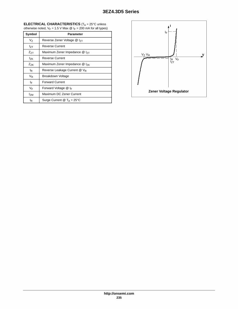
Zener Voltage Regulator
IF
V
I
IRIZT
VRVZ
VF
3EZ4.3D5 Series
http://onsemi.com235
ELECTRICAL CHARACTERISTICS (TA = 25°C unlessotherwise noted, VF = 1.5 V Max @ IF = 200 mA for all types)
Symbol Parameter
VZ Reverse Zener Voltage @ IZT
IZT Reverse Current
ZZT Maximum Zener Impedance @ IZT
IZK Reverse Current
ZZK Maximum Zener Impedance @ IZK
IR Reverse Leakage Current @ VR
VR Breakdown Voltage
IF Forward Current
VF Forward Voltage @ IF
IZM Maximum DC Zener Current
IR Surge Current @ TA = 25°C

3EZ4.3D5 Series
http://onsemi.com236
ELECTRICAL CHARACTERISTICS (TA = 25°C unless otherwise noted, VF = 1.5 V Max @ IF = 200 mA for all types)
Zener Voltage (Note 2.) Zener Impedance (Note 3.) Leakage CurrentIR
Device DeviceVZ (Volts) @ IZT ZZT @ IZT ZZK @ IZK IR @ VR IZM
IR(Note 4.)
Device(Note 1.)
DeviceMarking Min Nom Max mA mA µA Max Volts mA mA
3EZ4.3D5 3EZ4.3D5 4.09 4.3 4.52 174 4.5 400 1 30 1 590 4.13EZ6.2D5 3EZ6.2D5 5.89 6.2 6.51 121 1.5 700 1 5 3 435 3.13EZ8.2D5 3EZ8.2D5 7.79 8.2 8.61 91 2.3 700 0.5 5 6 330 2.443EZ10D5 3EZ10D5 9.50 10 10.5 75 3.5 700 0.25 3 7.6 270 2.03EZ13D5 3EZ13D5 12.35 13 13.65 58 4.5 700 0.25 0.5 9.9 208 1.54
3EZ15D5 3EZ15D5 14.25 15 15.75 50 5.5 700 0.25 0.5 11.4 180 1.333EZ16D5 3EZ16D5 15.2 16 16.8 47 5.5 700 0.25 0.5 12.2 169 1.253EZ18D5 3EZ18D5 17.1 18 18.9 42 6.0 750 0.25 0.5 13.7 150 1.113EZ24D5 3EZ24D5 22.8 24 25.2 31 9.0 750 0.25 0.5 18.2 112 0.833EZ36D5 3EZ36D5 34.2 36 37.8 21 22 1000 0.25 0.5 27.4 75 0.56
3EZ39D5 3EZ39D5 37.05 39 40.95 19 28 1000 0.25 0.5 29.7 69 0.513EZ220D5 3EZ220D5 209 220 231 3.4 1600 9000 0.25 1 167 12 0.093EZ240D5 3EZ240D5 228 240 252 3.1 1700 9000 0.25 1 182 11 0.093EZ330D5 3EZ330D5 313.5 330 346.5 2.3 2200 9000 0.25 1 251 8 0.06
1. TOLERANCE AND TYPE NUMBER DESIGNATIONTolerance designation – device tolerance of ±5% are indicated by a “5” suffix.
2. ZENER VOLTAGE (VZ) MEASUREMENTON Semiconductor guarantees the zener voltage when measured at 40 ms ±10 ms, 3/8″ from the diode body. And an ambient temperatureof 25°C (+8°C, –2°C)
3. ZENER IMPEDANCE (ZZ) DERIVATIONThe zener impedance is derived from 60 seconds AC voltage, which results when an AC current having an rms value equal to 10% of theDC zener current (IZT or IZK) is superimposed on IZT or IZK.
4. SURGE CURRENT (IR) NON–REPETITIVEThe rating listed in the electrical characteristics table is maximum peak, non–repetitive, reverse surge current of 1/2 square wave orequivalent sine wave pulse of 1/120 second duration superimposed on the test current, IZT, per JEDEC standards. However, actual devicecapability is as described in Figure 3 of the General Data sheet for Surmetic 30s.
Figure 1. Power Temperature Derating Curve
TL, LEAD TEMPERATURE (°C)0 20 40 60 20080 100 120 140 160 180
0
1
2
3
4
5
L = 1/8″
L = 3/8″
L = 1″
L = LEAD LENGTH TO HEAT SINK
PD
, ST
EA
DY
STA
TE
PO
WE
RD
ISS
IPA
TIO
N (
WA
TT
S)

3EZ4.3D5 Series
http://onsemi.com237
t, TIME (SECONDS)
0.0001 0.0002 0.0005 0.001 0.002 0.005 0.01 0.02 0.05 0.1 0.2 0.5 1 2 5 100.3
0.5
0.7
1
2
3
5
710
20
30
D =0.5
0.2
0.1
0.05
0.01
D = 0
DUTY CYCLE, D =t1/t2
θ JL
(t, D
) TR
AN
SIE
NT
TH
ER
MA
L R
ES
ISTA
NC
E
JUN
CT
ION
TO
LE
AD
( C
/W)
°
PPK t1
NOTE: BELOW 0.1 SECOND, THERMAL RESPONSE CURVE IS APPLICABLE
TO ANY LEAD LENGTH (L).
SINGLE PULSE ∆TJL = θJL (t)PPKREPETITIVE PULSES ∆TJL = θJL (t,D)PPK
t2
0.02
10
20
30
50
100
200
300
500
1K
0.1 0.2 0.3 0.5 1 2 3 5 10 20 30 50 100
PW, PULSE WIDTH (ms)
P
, P
EA
K S
UR
GE
PO
WE
R (
WA
TT
S)
PK
1 2 5 10 20 50 100 200 400 10000.00030.0005
0.001
0.002
0.005
0.01
0.02
0.05
0.1
0.2
0.5
1
23
TA = 125°C
TA = 125°C
NOMINAL VZ (VOLTS)
AS
SP
EC
IFIE
D IN
ELE
C. C
HA
R. T
AB
LE
Figure 2. Typical Thermal Response L, Lead Length = 3/8 Inch
Figure 3. Maximum Surge Power Figure 4. Typical Reverse Leakage
I R, R
EV
ER
SE
LE
AK
AG
E (µ
Adc
) @
VRRECTANGULAR
NONREPETITIVE
WAVEFORMTJ=25°C PRIOR
TO INITIAL PULSE

3EZ4.3D5 Series
http://onsemi.com238
APPLICATION NOTE
Since the actual voltage available from a given zenerdiode is temperature dependent, it is necessary to determinejunction temperature under any set of operating conditionsin order to calculate its value. The following procedure isrecommended:
Lead Temperature, TL, should be determined from:
TL = θLA PD + TAθLA is the lead-to-ambient thermal resistance (°C/W) and PDis the power dissipation. The value for θLA will vary anddepends on the device mounting method. θLA is generally30–40°C/W for the various clips and tie points in commonuse and for printed circuit board wiring.
The temperature of the lead can also be measured using athermocouple placed on the lead as close as possible to thetie point. The thermal mass connected to the tie point isnormally large enough so that it will not significantlyrespond to heat surges generated in the diode as a result ofpulsed operation once steady-state conditions are achieved.Using the measured value of TL, the junction temperaturemay be determined by:
TJ = TL + ∆TJL
∆TJL is the increase in junction temperature above the leadtemperature and may be found from Figure 2 for a train ofpower pulses (L = 3/8 inch) or from Figure 10 for dc power.
∆TJL = θJL PD
For worst-case design, using expected limits of IZ, limitsof PD and the extremes of TJ (∆TJ) may be estimated.Changes in voltage, VZ, can then be found from:
∆V = θVZ ∆TJ
θVZ, the zener voltage temperature coefficient, is foundfrom Figures 5 and 6.
Under high power-pulse operation, the zener voltage willvary with time and may also be affected significantly by thezener resistance. For best regulation, keep currentexcursions as low as possible.
Data of Figure 2 should not be used to compute surgecapability. Surge limitations are given in Figure 3. They arelower than would be expected by considering only junctiontemperature, as current crowding effects cause temperaturesto be extremely high in small spots resulting in devicedegradation should the limits of Figure 3 be exceeded.

3EZ4.3D5 Series
http://onsemi.com239
Figure 5. Units To 12 Volts Figure 6. Units 10 To 400 Volts
Figure 7. V Z = 3.3 thru 10 Volts Figure 8. V Z = 12 thru 82 Volts
Figure 9. V Z = 100 thru 400 Volts Figure 10. Typical Thermal Resistance
ZENER VOLTAGE versus ZENER CURRENT(Figures 7, 8 and 9)
TEMPERATURE COEFFICIENT RANGES(90% of the Units are in the Ranges Indicated)
VZ, ZENER VOLTAGE @ IZT (VOLTS)
3 4 5 6 7 8 9 10 11 12
10
8
6
4
2
0
-2
-4
RANGE
, TE
MP
ER
ATU
RE
CO
EF
FIC
IEN
T (m
V/
C)
@ I
ZT
VZ
°θ
1000
500
200
100
50
20
1010 20 50 100 200 400 1000
VZ, ZENER VOLTAGE @ IZT (VOLTS)
, TE
MP
ER
ATU
RE
CO
EF
FIC
IEN
T (m
V/
C)
@ I Z
TV
Z°
θ
0 1 2 3 4 5 6 7 8 9 10
100
50
3020
10
1
0.5
0.30.2
0.1
VZ, ZENER VOLTAGE (VOLTS)
I , Z
EN
ER
CU
RR
EN
T (m
A)
Z
2
5
3
0 10 20 30 40 50 60 70 80 90 100
VZ, ZENER VOLTAGE (VOLTS)
I ,
ZE
NE
R C
UR
RE
NT
(mA
)Z
100
50
3020
10
1
0.5
0.30.2
0.1
2
53
100 200 300 400250 350150
10
1
0.5
0.2
0.1
VZ, ZENER VOLTAGE (VOLTS)
2
5
I ,
ZE
NE
R C
UR
RE
NT
(mA
)Z
0
10
20
30
40
50
60
70
80
L, LEAD LENGTH TO HEAT SINK (INCH)
PRIMARY PATH OFCONDUCTION IS THROUGH
THE CATHODE LEAD
0 1/8 1/4 3/8 1/2 5/8 3/4 7/8 1
TL
JL, J
UN
CT
ION
TO
LE
AD
TH
ER
MA
L R
ES
ISTA
NC
Eθ
LL
( C
/W)
°

Semiconductor Components Industries, LLC, 2001
May, 2001 – Rev. 1240 Publication Order Number:
MZP4729A/D
MZP4729A Series
3 Watt DO-41 Surmetic 30Zener Voltage Regulators
This is a complete series of 3 Watt Zener diodes with limits andexcellent operating characteristics that reflect the superior capabilitiesof silicon–oxide passivated junctions. All this in an axial–lead,transfer–molded plastic package that offers protection in all commonenvironmental conditions.
Specification Features:• Zener Voltage Range – 3.6 V to 30 V
• ESD Rating of Class 3 (>16 KV) per Human Body Model
• Surge Rating of 98 W @ 1 ms
• Maximum Limits Guaranteed on up to Six Electrical Parameters
• Package No Larger than the Conventional 1 Watt Package
Mechanical Characteristics:CASE: Void free, transfer–molded, thermosetting plasticFINISH: All external surfaces are corrosion resistant and leads arereadily solderableMAXIMUM LEAD TEMPERATURE FOR SOLDERING PURPOSES:230°C, 1/16″ from the case for 10 secondsPOLARITY: Cathode indicated by polarity bandMOUNTING POSITION: Any
MAXIMUM RATINGS
Rating Symbol Value Unit
Max. Steady State Power Dissipation@ TL = 75°C, Lead Length = 3/8″Derate above 75°C
PD 3
24
W
mW/°C
Steady State Power Dissipation@ TA = 50°CDerate above 50°C
PD 1
6.67
W
mW/°C
Operating and StorageTemperature Range
TJ, Tstg –65 to+200
°C
Device Package Shipping
ORDERING INFORMATION
MZP47xxA Axial Lead 2000 Units/Box
MZP47xxARL Axial Lead
AXIAL LEADCASE 59PLASTIC
http://onsemi.com
6000/Tape & Reel
Cathode Anode
Polarity band up with cathode lead off first Polarity band down with cathode lead off first
LMZP47xxAYYWW
L = Assembly LocationMZP47xxA = Device Code
= (See Table Next Page)YY = YearWW = Work Week
MARKING DIAGRAM
MZP47xxATA Axial Lead 4000/Ammo Pack
MZP47xxARR1 Axial Lead 2000/Tape & Reel
MZP47xxARR2 Axial Lead 2000/Tape & Reel

Zener Voltage Regulator
IF
V
I
IRIZT
VRVZ
VF
MZP4729A Series
http://onsemi.com241
ELECTRICAL CHARACTERISTICS (TA = 25°C unlessotherwise noted, VF = 1.5 V Max @ IF = 200 mA for all types)
Symbol Parameter
VZ Reverse Zener Voltage @ IZT
IZT Reverse Current
ZZT Maximum Zener Impedance @ IZT
IZK Reverse Current
ZZK Maximum Zener Impedance @ IZK
IR Reverse Leakage Current @ VR
VR Breakdown Voltage
IF Forward Current
VF Forward Voltage @ IF
IR Surge Current @ TA = 25°C

MZP4729A Series
http://onsemi.com242
ELECTRICAL CHARACTERISTICS (TA = 25°C unless otherwise noted, VF = 1.5 V Max @ IF = 200 mA for all types)
Zener Voltage (Note 2.) Zener Impedance (Note 3.) Leakage CurrentIR
Device DeviceVZ (Volts) @ IZT ZZT @ IZT ZZK @ IZK IR @ VR
IR(Note 4.)
Device(Note 1.)
DeviceMarking Min Nom Max mA mA µA Max Volts mA
MZP4729A MZP4729A 3.42 3.6 3.78 69 10 400 1 100 1 1260MZP4734A MZP4734A 5.32 5.6 5.88 45 5 600 1 10 2 810MZP4735A MZP4735A 5.89 6.2 6.51 41 2 700 1 10 3 730MZP4736A MZP4736A 6.46 6.8 7.14 37 3.5 700 1 10 4 660MZP4737A MZP4737A 7.13 7.5 7.88 34 4 700 0.5 10 5 605
MZP4738A MZP4738A 7.79 8.2 8.61 31 4.5 700 0.5 10 6 550MZP4740A MZP4740A 9.50 10 10.50 25 7 700 0.25 10 7.6 454MZP4741A MZP4741A 10.45 11 11.55 23 8 700 0.25 5 8.4 414MZP4744A MZP4744A 14.25 15 15.75 17 14 700 0.25 5 11.4 304MZP4745A MZP4745A 15.20 16 16.80 15.5 16 700 0.25 5 12.2 285
MZP4746A MZP4746A 17.10 18 18.90 14 20 750 0.25 5 13.7 250MZP4749A MZP4749A 22.80 24 25.20 10.5 25 750 0.25 5 18.2 190MZP4750A MZP4750A 25.65 27 28.35 9.5 35 750 0.25 5 20.6 170MZP4751A MZP4751A 28.50 30 31.50 8.5 40 1000 0.25 5 22.8 150MZP4752A MZP4752A 31.35 33 34.65 7.5 45 1000 0.25 5 25.1 135
MZP4753A MZP4753A 34.20 36 37.80 7.0 50 1000 0.25 5 27.4 125
1. TOLERANCE AND TYPE NUMBER DESIGNATIONThe type numbers listed have a standard tolerance on the nominal zener voltage of ±5%.
2. ZENER VOLTAGE (VZ) MEASUREMENTON Semiconductor guarantees the zener voltage when measured at 90 seconds while maintaining the lead temperature (TL) at 30°C ±1°C,3/8″ from the diode body.
3. ZENER IMPEDANCE (ZZ) DERIVATIONThe zener impedance is derived from 60 seconds AC voltage, which results when an AC current having an rms value equal to 10% of theDC zener current (IZT or IZK) is superimposed on IZT or IZK.
4. SURGE CURRENT (IR) NON–REPETITIVEThe rating listed in the electrical characteristics table is maximum peak, non–repetitive, reverse surge current of 1/2 square wave orequivalent sine wave pulse of 1/120 second duration superimposed on the test current, IZT, per JEDEC standards. However, actual devicecapability is as described in Figure 3 of the General Data sheet for Surmetic 30s.
Figure 1. Power Temperature Derating Curve
TL, LEAD TEMPERATURE (°C)0 20 40 60 20080 100 120 140 160 180
0
1
2
3
4
5
L = 1/8″
L = 3/8″
L = 1″
L = LEAD LENGTH TO HEAT SINK
PD
, MA
XIM
UM
ST
EA
DY
STA
TE
PO
WE
R D
ISS
IPA
TIO
N (
WA
TT
S)

MZP4729A Series
http://onsemi.com243
t, TIME (SECONDS)
0.0001 0.0002 0.0005 0.001 0.002 0.005 0.01 0.02 0.05 0.1 0.2 0.5 1 2 5 100.3
0.5
0.7
1
2
3
5
710
20
30
D =0.5
0.2
0.1
0.05
0.01
D = 0
DUTY CYCLE, D =t1/t2
θ JL
(t, D
) TR
AN
SIE
NT
TH
ER
MA
L R
ES
ISTA
NC
E
JUN
CT
ION
TO
LE
AD
( C
/W)
°
PPK t1
NOTE: BELOW 0.1 SECOND, THERMAL RESPONSE CURVE IS APPLICABLE
TO ANY LEAD LENGTH (L).
SINGLE PULSE ∆TJL = θJL (t)PPKREPETITIVE PULSES ∆TJL = θJL (t,D)PPK
t2
0.02
10
20
30
50
100
200
300
500
1K
0.1 0.2 0.3 0.5 1 2 3 5 10 20 30 50 100
PW, PULSE WIDTH (ms)
P
, P
EA
K S
UR
GE
PO
WE
R (
WA
TT
S)
PK
1 2 5 10 20 50 100 200 400 10000.00030.0005
0.001
0.002
0.005
0.01
0.02
0.05
0.1
0.2
0.5
1
23
TA = 125°C
TA = 125°C
NOMINAL VZ (VOLTS)
AS
SP
EC
IFIE
D IN
ELE
C. C
HA
R. T
AB
LE
Figure 2. Typical Thermal Response L, Lead Length = 3/8 Inch
Figure 3. Maximum Surge Power Figure 4. Typical Reverse Leakage
I R, R
EV
ER
SE
LE
AK
AG
E (µ
Adc
) @
VRRECTANGULAR
NONREPETITIVE
WAVEFORMTJ=25°C PRIOR
TO INITIAL PULSE

MZP4729A Series
http://onsemi.com244
APPLICATION NOTE
Since the actual voltage available from a given zenerdiode is temperature dependent, it is necessary to determinejunction temperature under any set of operating conditionsin order to calculate its value. The following procedure isrecommended:
Lead Temperature, TL, should be determined from:
TL = θLA PD + TAθLA is the lead-to-ambient thermal resistance (°C/W) and PDis the power dissipation. The value for θLA will vary anddepends on the device mounting method. θLA is generally30–40°C/W for the various clips and tie points in commonuse and for printed circuit board wiring.
The temperature of the lead can also be measured using athermocouple placed on the lead as close as possible to thetie point. The thermal mass connected to the tie point isnormally large enough so that it will not significantlyrespond to heat surges generated in the diode as a result ofpulsed operation once steady-state conditions are achieved.Using the measured value of TL, the junction temperaturemay be determined by:
TJ = TL + ∆TJL
∆TJL is the increase in junction temperature above the leadtemperature and may be found from Figure 2 for a train ofpower pulses (L = 3/8 inch) or from Figure 10 for dc power.
∆TJL = θJL PD
For worst-case design, using expected limits of IZ, limitsof PD and the extremes of TJ (∆TJ) may be estimated.Changes in voltage, VZ, can then be found from:
∆V = θVZ ∆TJ
θVZ, the zener voltage temperature coefficient, is foundfrom Figures 5 and 6.
Under high power-pulse operation, the zener voltage willvary with time and may also be affected significantly by thezener resistance. For best regulation, keep currentexcursions as low as possible.
Data of Figure 2 should not be used to compute surgecapability. Surge limitations are given in Figure 3. They arelower than would be expected by considering only junctiontemperature, as current crowding effects cause temperaturesto be extremely high in small spots resulting in devicedegradation should the limits of Figure 3 be exceeded.

MZP4729A Series
http://onsemi.com245
Figure 5. Units To 12 Volts Figure 6. Units 10 To 400 Volts
Figure 7. V Z = 3.3 thru 10 Volts Figure 8. V Z = 12 thru 82 Volts
Figure 9. V Z = 100 thru 400 Volts Figure 10. Typical Thermal Resistance
ZENER VOLTAGE versus ZENER CURRENT(Figures 7, 8 and 9)
TEMPERATURE COEFFICIENT RANGES(90% of the Units are in the Ranges Indicated)
VZ, ZENER VOLTAGE @ IZT (VOLTS)
3 4 5 6 7 8 9 10 11 12
10
8
6
4
2
0
-2
-4
RANGE
, TE
MP
ER
ATU
RE
CO
EF
FIC
IEN
T (m
V/
C)
@ I
ZT
VZ
°θ
1000
500
200
100
50
20
1010 20 50 100 200 400 1000
VZ, ZENER VOLTAGE @ IZT (VOLTS)
, TE
MP
ER
ATU
RE
CO
EF
FIC
IEN
T (m
V/
C)
@ I Z
TV
Z°
θ
0 1 2 3 4 5 6 7 8 9 10
100
50
3020
10
1
0.5
0.30.2
0.1
VZ, ZENER VOLTAGE (VOLTS)
I , Z
EN
ER
CU
RR
EN
T (m
A)
Z
2
5
3
0 10 20 30 40 50 60 70 80 90 100
VZ, ZENER VOLTAGE (VOLTS)
I ,
ZE
NE
R C
UR
RE
NT
(mA
)Z
100
50
3020
10
1
0.5
0.30.2
0.1
2
53
100 200 300 400250 350150
10
1
0.5
0.2
0.1
VZ, ZENER VOLTAGE (VOLTS)
2
5
I ,
ZE
NE
R C
UR
RE
NT
(mA
)Z
0
10
20
30
40
50
60
70
80
L, LEAD LENGTH TO HEAT SINK (INCH)
PRIMARY PATH OFCONDUCTION IS THROUGH
THE CATHODE LEAD
0 1/8 1/4 3/8 1/2 5/8 3/4 7/8 1
TL
JL, J
UN
CT
ION
TO
LE
AD
TH
ER
MA
L R
ES
ISTA
NC
Eθ
LL
( C
/W)
°

Semiconductor Components Industries, LLC, 2001
May, 2001 – Rev. 1246 Publication Order Number:
1N5333B/D
1N5333B Series
5 Watt Surmetic 40Zener Voltage Regulators
This is a complete series of 5 Watt Zener diodes with tight limits andbetter operating characteristics that reflect the superior capabilities ofsilicon–oxide passivated junctions. All this in an axial–lead,transfer–molded plastic package that offers protection in all commonenvironmental conditions.
Specification Features:• Zener Voltage Range – 3.3 V to 200 V
• ESD Rating of Class 3 (>16 KV) per Human Body Model
• Surge Rating of up to 180 W @ 8.3 ms
• Maximum Limits Guaranteed on up to Six Electrical Parameters
Mechanical Characteristics:CASE: Void free, transfer–molded, thermosetting plasticFINISH: All external surfaces are corrosion resistant and leads arereadily solderableMAXIMUM LEAD TEMPERATURE FOR SOLDERING PURPOSES:230°C, 1/16″ from the case for 10 secondsPOLARITY: Cathode indicated by polarity bandMOUNTING POSITION: Any
MAXIMUM RATINGS
Rating Symbol Value Unit
Max. Steady State Power Dissipation@ TL = 75°C, Lead Length = 3/8″Derate above 75°C
PD 5
40
W
mW/°C
Operating and StorageTemperature Range
TJ, Tstg –65 to+200
°C
Device Package Shipping
ORDERING INFORMATION
1N53xxB Axial Lead 1000 Units/Box
1N53xxBRL Axial Lead
AXIAL LEADCASE 17PLASTIC
http://onsemi.com
4000/Tape & Reel
Cathode Anode
L1N53xxBYWW
L = Assembly Location1N53xxB = Device Code
= (See Table Next Page)Y = YearWW = Work Week
MARKING DIAGRAM
1N53xxBTA Axial Lead 2000/Ammo Pack
Devices listed in bold, italic are ON SemiconductorPreferred devices. Preferred devices are recommendedchoices for future use and best overall value.

Zener Voltage Regulator
IF
V
I
IRIZT
VRVZ
VF
1N5333B Series
http://onsemi.com247
ELECTRICAL CHARACTERISTICS (TA = 25°C unlessotherwise noted, VF = 1.2 V Max @ IF = 1.0 A for all types)
Symbol Parameter
VZ Reverse Zener Voltage @ IZT
IZT Reverse Current
ZZT Maximum Zener Impedance @ IZT
IZK Reverse Current
ZZK Maximum Zener Impedance @ IZK
IR Reverse Leakage Current @ VR
VR Breakdown Voltage
IF Forward Current
VF Forward Voltage @ IF
IR Maximum Surge Current @ TA = 25°C
VZ Reverse Zener Voltage Change
IZM Maximum DC Zener Current

1N5333B Series
http://onsemi.com248
ELECTRICAL CHARACTERISTICS (TA = 25°C unless otherwise noted, VF = 1.2 V Max @ IF = 1.0 A for all types)
Zener Voltage (Note 2.) Zener Impedance (Note 2.)LeakageCurrent
IR VZ IZM
Device DeviceVZ (Volts) @ IZT ZZT @ IZT ZZK @ IZK IZK IR @ VR
IR(Note 3.)
VZ(Note 4.)
IZM(Note 5.)
Device(Note 1.)
DeviceMarking Min Nom Max mA A µA Max Volts A Volts mA
1N5333B 1N5333B 3.14 3.3 3.47 380 3 400 1 300 1 20 0.85 14401N5334B 1N5334B 3.42 3.6 3.78 350 2.5 500 1 150 1 18.7 0.8 13201N5335B 1N5335B 3.71 3.9 4.10 320 2 500 1 50 1 17.6 0.54 12201N5336B 1N5336B 4.09 4.3 4.52 290 2 500 1 10 1 16.4 0.49 11001N5337B 1N5337B 4.47 4.7 4.94 260 2 450 1 5 1 15.3 0.44 1010
1N5338B 1N5338B 4.85 5.1 5.36 240 1.5 400 1 1 1 14.4 0.39 9301N5339B 1N5339B 5.32 5.6 5.88 220 1 400 1 1 2 13.4 0.25 8651N5340B 1N5340B 5.70 6.0 6.30 200 1 300 1 1 3 12.7 0.19 7901N5341B 1N5341B 5.89 6.2 6.51 200 1 200 1 1 3 12.4 0.1 7651N5342B 1N5342B 6.46 6.8 7.14 175 1 200 1 10 5.2 11.5 0.15 700
1N5343B 1N5343B 7.13 7.5 7.88 175 1.5 200 1 10 5.7 10.7 0.15 6301N5344B 1N5344B 7.79 8.2 8.61 150 1.5 200 1 10 6.2 10 0.2 5801N5345B 1N5345B 8.27 8.7 9.14 150 2 200 1 10 6.6 9.5 0.2 5451N5346B 1N5346B 8.65 9.1 9.56 150 2 150 1 7.5 6.9 9.2 0.22 5201N5347B 1N5347B 9.50 10 10.5 125 2 125 1 5 7.6 8.6 0.22 475
1N5348B 1N5348B 10.45 11 11.55 125 2.5 125 1 5 8.4 8.0 0.25 4301N5349B 1N5349B 11.4 12 12.6 100 2.5 125 1 2 9.1 7.5 0.25 3951N5350B 1N5350B 12.35 13 13.65 100 2.5 100 1 1 9.9 7.0 0.25 3651N5351B 1N5351B 13.3 14 14.7 100 2.5 75 1 1 10.6 6.7 0.25 3401N5352B 1N5352B 14.25 15 15.75 75 2.5 75 1 1 11.5 6.3 0.25 315
1N5353B 1N5353B 15.2 16 16.8 75 2.5 75 1 1 12.2 6.0 0.3 2951N5354B 1N5354B 16.15 17 17.85 70 2.5 75 1 0.5 12.9 5.8 0.35 2801N5355B 1N5355B 17.1 18 18.9 65 2.5 75 1 0.5 13.7 5.5 0.4 2641N5356B 1N5356B 18.05 19 19.95 65 3 75 1 0.5 14.4 5.3 0.4 2501N5357B 1N5357B 19 20 21 65 3 75 1 0.5 15.2 5.1 0.4 237
1N5358B 1N5358B 20.9 22 23.1 50 3.5 75 1 0.5 16.7 4.7 0.45 2161N5359B 1N5359B 22.8 24 25.2 50 3.5 100 1 0.5 18.2 4.4 0.55 1981N5360B 1N5360B 23.75 25 26.25 50 4 110 1 0.5 19 4.3 0.55 1901N5361B 1N5361B 25.65 27 28.35 50 5 120 1 0.5 20.6 4.1 0.6 1761N5362B 1N5362B 26.6 28 29.4 50 6 130 1 0.5 21.2 3.9 0.6 170
1. TOLERANCE AND TYPE NUMBER DESIGNATIONThe JEDEC type numbers shown indicate a tolerance of ±5%.
2. ZENER VOLTAGE (VZ) and IMPEDANCE (I ZT and IZK)Test conditions for zener voltage and impedance are as follows: IZ is applied 40 ±10 ms prior to reading. Mounting contacts are located 3/8″to 1/2″ from the inside edge of mounting clips to the body of the diode (TA = 25°C +8°C, –2°C).
3. SURGE CURRENT (IR)Surge current is specified as the maximum allowable peak, non–recurrent square–wave current with a pulse width, PW, of 8.3 ms. The datagiven in Figure 6 may be used to find the maximum surge current for a square wave of any pulse width between 1 ms and 1000 ms by plottingthe applicable points on logarithmic paper. Examples of this, using the 3.3 V and 200 V zener are shown in Figure 7. Mounting contact locatedas specified in Note 2 (TA = 25°C +8°C, –2°C).
4. VOLTAGE REGULATION ( VZ)The conditions for voltage regulation are as follows: VZ measurements are made at 10% and then at 50% of the IZ max value listed in theelectrical characteristics table. The test current time duration for each VZ measurement is 40 ±10 ms. Mounting contact located as specifiedin Note 2 (TA = 25°C +8°C, –2°C).
5. MAXIMUM REGULATOR CURRENT (I ZM)The maximum current shown is based on the maximum voltage of a 5% type unit, therefore, it applies only to the B–suffix device. The actualIZM for any device may not exceed the value of 5 watts divided by the actual VZ of the device. TL = 75°C at 3/8″ maximum from the devicebody.

1N5333B Series
http://onsemi.com249
ELECTRICAL CHARACTERISTICS (TA = 25°C unless otherwise noted, VF = 1.2 V Max @ IF = 1.0 A for all types)
Zener Voltage (Note 7.) Zener Impedance (Note 7.)LeakageCurrent
IR VZ IZM
Device DeviceVZ (Volts) @ IZT ZZT @ IZT ZZK @ IZK IZK IR @ VR
IR(Note 8.)
VZ(Note 9.)
IZM(Note 10.)
Device(Note 6.)
DeviceMarking Min Nom Max mA A µA Max Volts A Volts mA
1N5363B 1N5363B 28.5 30 31.5 40 8 140 1 0.5 22.8 3.7 0.6 1581N5364B 1N5364B 31.35 33 34.65 40 10 150 1 0.5 25.1 3.5 0.6 1441N5365B 1N5365B 34.2 36 37.8 30 11 160 1 0.5 27.4 3.5 0.65 1321N5366B 1N5366B 37.05 39 40.95 30 14 170 1 0.5 29.7 3.1 0.65 1221N5367B 1N5367B 40.85 43 45.15 30 20 190 1 0.5 32.7 2.8 0.7 110
1N5368B 1N5368B 44.65 47 49.35 25 25 210 1 0.5 35.8 2.7 0.8 1001N5369B 1N5369B 48.45 51 53.55 25 27 230 1 0.5 38.8 2.5 0.9 931N5370B 1N5370B 53.2 56 58.8 20 35 280 1 0.5 42.6 2.3 1.0 861N5371B 1N5371B 57 60 63 20 40 350 1 0.5 45.5 2.2 1.2 791N5372B 1N5372B 58.9 62 65.1 20 42 400 1 0.5 47.1 2.1 1.35 76
1N5373B 1N5373B 64.6 68 71.4 20 44 500 1 0.5 51.7 2.0 1.52 701N5374B 1N5374B 71.25 75 78.75 20 45 620 1 0.5 56 1.9 1.6 631N5375B 1N5375B 77.9 82 86.1 15 65 720 1 0.5 62.2 1.8 1.8 581N5376B 1N5376B 82.65 87 91.35 15 75 760 1 0.5 66 1.7 2.0 54.51N5377B 1N5377B 86.45 91 95.55 15 75 760 1 0.5 69.2 1.6 2.2 52.5
1N5378B 1N5378B 95 100 105 12 90 800 1 0.5 76 1.5 2.5 47.51N5379B 1N5379B 104.5 110 115.5 12 125 1000 1 0.5 83.6 1.4 2.5 431N5380B 1N5380B 114 120 126 10 170 1150 1 0.5 91.2 1.3 2.5 39.51N5381B 1N5381B 123.5 130 136.5 10 190 1250 1 0.5 98.8 1.2 2.5 36.61N5382B 1N5382B 133 140 147 8 230 1500 1 0.5 106 1.2 2.5 34
1N5383B 1N5383B 142.5 150 157.5 8 330 1500 1 0.5 114 1.1 3.0 31.61N5384B 1N5384B 152 160 168 8 350 1650 1 0.5 122 1.1 3.0 29.41N5385B 1N5385B 161.5 170 178.5 8 380 1750 1 0.5 129 1.0 3.0 281N5386B 1N5386B 171 180 189 5 430 1750 1 0.5 137 1.0 4.0 26.41N5387B 1N5387B 180.5 190 199.5 5 450 1850 1 0.5 144 0.9 5.0 25
1N5388B 1N5388B 190 200 210 5 480 1850 1 0.5 152 0.9 5.0 23.6
6. TOLERANCE AND TYPE NUMBER DESIGNATIONThe JEDEC type numbers shown indicate a tolerance of ±5%.
7. ZENER VOLTAGE (VZ) and IMPEDANCE (I ZT and IZK)Test conditions for zener voltage and impedance are as follows: IZ is applied 40 ±10 ms prior to reading. Mounting contacts are located 3/8″to 1/2″ from the inside edge of mounting clips to the body of the diode (TA = 25°C +8°C, –2°C).
8. SURGE CURRENT (IR)Surge current is specified as the maximum allowable peak, non–recurrent square–wave current with a pulse width, PW, of 8.3 ms. The datagiven in Figure 6 may be used to find the maximum surge current for a square wave of any pulse width between 1 ms and 1000 ms by plottingthe applicable points on logarithmic paper. Examples of this, using the 3.3 V and 200 V zener are shown in Figure 7. Mounting contact locatedas specified in Note 7 (TA = 25°C +8°C, –2°C).
9. VOLTAGE REGULATION ( VZ)The conditions for voltage regulation are as follows: VZ measurements are made at 10% and then at 50% of the IZ max value listed in theelectrical characteristics table. The test current time duration for each VZ measurement is 40 ±10 ms. Mounting contact located as specifiedin Note 7 (TA = 25°C +8°C, –2°C).
10.MAXIMUM REGULATOR CURRENT (I ZM)The maximum current shown is based on the maximum voltage of a 5% type unit, therefore, it applies only to the B–suffix device. The actualIZM for any device may not exceed the value of 5 watts divided by the actual VZ of the device. TL = 75°C at 3/8″ maximum from the devicebody.

1N5333B Series
http://onsemi.com250
Figure 1. Power Temperature Derating Curve
TL, LEAD TEMPERATURE (°C)
PD
, MA
XIM
UM
ST
EA
DY
STA
TE
PO
WE
R D
ISS
IPA
TIO
N (
WA
TT
S)
8
6
4
2
00 20 40 60 80 100 120 140 160 180 200
L=LEAD LENGTH
L=TO HEAT SINK
L=(SEE FIGURE 5)L=1/8″
L=3/8″
L=1″
TEMPERATURE COEFFICIENTS
Figure 2. Temperature Coefficient-Rangefor Units 3 to 10 Volts
Figure 3. Temperature Coefficient-Rangefor Units 10 to 220 Volts
VZ, ZENER VOLTAGE @ IZT (VOLTS)
10
8
6
4
2
0
-2
3 4 5 6 7 8 9 10
RANGE
300
200
100
50
30
20
10
5
0 20 40 60 80 100 120 140 160 180 200 220
VZ, ZENER VOLTAGE @ IZT (VOLTS)
θVZ
, TE
MP
ER
ATU
RE
CO
EF
FIC
IEN
T
(mV
/°C)
@ I
ZT
θVZ
, TE
MP
ER
ATU
RE
CO
EF
FIC
IEN
T
(mV
/°C)
@ I
ZT RANGE

1N5333B Series
http://onsemi.com251
Figure 4. Typical Thermal ResponseL, Lead Length = 3/8 Inch
Figure 5. Typical Thermal Resistance Figure 6. Maximum Non-Repetitive Surge Currentversus Nominal Zener Voltage
(See Note 3)
θ JL
(t, D
), T
RA
NS
IEN
T T
HE
RM
AL
RE
SIS
TAN
CE
JUN
CT
ION
TO
LE
AD
(°C
/W)
20
10
5
2
1
0.5
0.20.00
10.00
50.01 0.05 0.1 0.5 1 5 10 20 50 100
D = 0.5
D = 0.2
D = 0.1
D = 0.05
D = 0.01
D = 0
NOTE: BELOW 0.1 SECOND, THERMALNOTE: RESPONSE CURVE IS APPLICABLENOTE: TO ANY LEAD LENGTH (L).
DUTY CYCLE, D = t1/t2SINGLE PULSE ∆ TJL = θJL(t)PPK
REPETITIVE PULSES ∆ TJL = θJL(t, D)PPK
PPK t1
t2
t, TIME (SECONDS)
40
30
20
10
00 0.2 0.4 0.6 0.8 1
PRIMARY PATH OFCONDUCTION IS THROUGH
THE CATHODE LEAD
L L
L, LEAD LENGTH TO HEAT SINK (INCH)JL, J
UN
CT
ION
TO
LE
AD
TH
ER
MA
L R
ES
ISTA
NC
E (
θ°C
/W)
I r, P
EA
K S
UR
GE
CU
RR
EN
T (A
MP
S)
40
20
10
4
2
1
0.1
0.2
0.4
3 4 6 8 10 20 30 40 60 80 100 200
*SQUARE WAVE PW=100ms*
PW=1000ms*
PW=1ms*
PW=8.3ms*
NOMINAL VZ (V)
3020
10
0.1
0.2
0.5
1
2
5
1 10 100 1000
1000
100
10
1
0.11 2 3 4 5 6 7 8 9 10
I Z, Z
EN
ER
CU
RR
EN
T (m
A)
PW, PULSE WIDTH (ms) VZ, ZENER VOLTAGE (VOLTS)
Figure 7. Peak Surge Current versus Pulse Width(See Note 3)
Figure 8. Zener Voltage versus Zener CurrentVZ = 3.3 thru 10 Volts
VZ=200V
VZ=3.3V
PLOTTED FROM INFORMATIONGIVEN IN FIGURE 6
TC=25°C
T=25°C
I r, P
EA
K S
UR
GE
CU
RR
EN
T (A
MP
S)
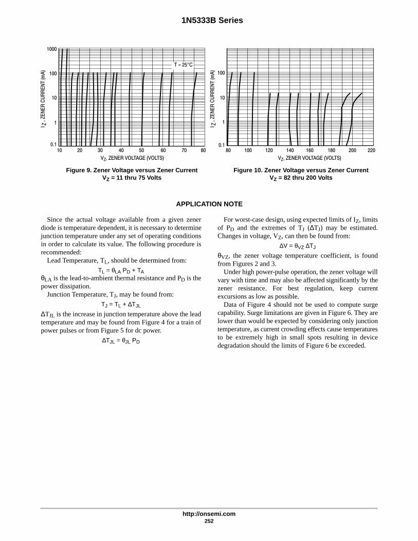
1N5333B Series
http://onsemi.com252
I Z, Z
EN
ER
CU
RR
EN
T (m
A)
VZ, ZENER VOLTAGE (VOLTS)
1000
100
10
1
0.110 20 30 40 50 60 70 80
100
10
1
0.180 100 120 140 160 180 200 220
VZ, ZENER VOLTAGE (VOLTS)
I Z, Z
EN
ER
CU
RR
EN
T (m
A)
T=25°C
Figure 9. Zener Voltage versus Zener CurrentVZ = 11 thru 75 Volts
Figure 10. Zener Voltage versus Zener CurrentVZ = 82 thru 200 Volts
APPLICATION NOTE
Since the actual voltage available from a given zenerdiode is temperature dependent, it is necessary to determinejunction temperature under any set of operating conditionsin order to calculate its value. The following procedure isrecommended:
Lead Temperature, TL, should be determined from:
TL = θLA PD + TAθLA is the lead-to-ambient thermal resistance and PD is thepower dissipation.
Junction Temperature, TJ, may be found from:
TJ = TL + ∆TJL
∆TJL is the increase in junction temperature above the leadtemperature and may be found from Figure 4 for a train ofpower pulses or from Figure 5 for dc power.
∆TJL = θJL PD
For worst-case design, using expected limits of IZ, limitsof PD and the extremes of TJ (∆TJ) may be estimated.Changes in voltage, VZ, can then be found from:
∆V = θVZ ∆TJ
θVZ, the zener voltage temperature coefficient, is foundfrom Figures 2 and 3.
Under high power-pulse operation, the zener voltage willvary with time and may also be affected significantly by thezener resistance. For best regulation, keep currentexcursions as low as possible.
Data of Figure 4 should not be used to compute surgecapability. Surge limitations are given in Figure 6. They arelower than would be expected by considering only junctiontemperature, as current crowding effects cause temperaturesto be extremely high in small spots resulting in devicedegradation should the limits of Figure 6 be exceeded.

http://onsemi.com253
CHAPTER 7Zener Voltage Regulator Diodes –
Surface Mounted Data Sheets

Semiconductor Components Industries, LLC, 2001
May, 2001 – Rev. 5254 Publication Order Number:
MM3Z2V4T1/D
MM3Z2V4T1 SERIES
Zener Voltage Regulators
200 mW SOD–323 Surface MountThis series of Zener diodes is packaged in a SOD–323 surface
mount package that has a power dissipation of 200 mW. They aredesigned to provide voltage regulation protection and are especiallyattractive in situations where space is at a premium. They are wellsuited for applications such as cellular phones, hand held portables,and high density PC boards.
Specification Features:• Standard Zener Breakdown Voltage Range – 2.4 V to 75 V
• Steady State Power Rating of 200 mW
• Small Body Outline Dimensions:0.067″ x 0.049″ (1.7 mm x 1.25 mm)
• Low Body Height: 0.035″ (0.9 mm)
• Package Weight: 4.507 mg/unit
• ESD Rating of Class 3 (>16 KV) per Human Body Model
Mechanical Characteristics:CASE: Void-free, transfer-molded plasticFINISH: All external surfaces are corrosion resistantMAXIMUM CASE TEMPERATURE FOR SOLDERING PURPOSES:
260°C for 10 SecondsLEADS: Plated with Pb/Sn for ease of solderabilityPOLARITY: Cathode indicated by polarity bandFLAMMABILITY RATING: UL94 V–0MOUNTING POSITION: Any
MAXIMUM RATINGS
Rating Symbol Max Unit
Total Device Dissipation FR–5 Board,(Note 1.) @ TA = 25°CDerate above 25°C
PD2001.5
mWmW/°C
Thermal Resistance fromJunction to Ambient
RJA 635 °C/W
Junction and StorageTemperature Range
TJ, Tstg –65 to+150
°C
1. FR–4 Minimum Pad
Device Package Shipping
ORDERING INFORMATION
SOD–323CASE 477–02
STYLE 1
http://onsemi.com
1Cathode
2Anode
MM3ZxxxT1 SOD–323 3000/Tape & Reel
MARKING DIAGRAM
See specific marking information in the device markingcolumn of the Electrical Characteristics table on page 256 ofthis data sheet.
DEVICE MARKING INFORMATION
xx = Specific Device CodeM = Date Code
xx M
†The “T1” suffix refers to an 8 mm, 7 inch reel.

Zener Voltage Regulator
IF
V
I
IRIZT
VRVZVF
MM3Z2V4T1 SERIES
http://onsemi.com255
ELECTRICAL CHARACTERISTICS(TA = 25°C unless otherwise noted,VF = 0.9 V Max. @ IF = 10 mA for all types)
Symbol Parameter
VZ Reverse Zener Voltage @ IZT
IZT Reverse Current
ZZT Maximum Zener Impedance @ IZT
IZK Reverse Current
ZZK Maximum Zener Impedance @ IZK
IR Reverse Leakage Current @ VR
VR Reverse Voltage
IF Forward Current
VF Forward Voltage @ IF
VZ Maximum Temperature Coefficient of VZ
C Max. Capacitance @VR = 0 and f = 1 MHz
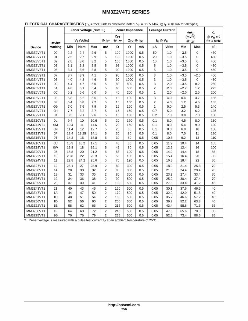
MM3Z2V4T1 SERIES
http://onsemi.com256
ELECTRICAL CHARACTERISTICS (TA = 25°C unless otherwise noted, VF = 0.9 V Max. @ IF = 10 mA for all types)
Zener Voltage (Note 2.) Zener Impedance Leakage CurrentVZ C
DeviceVZ (Volts) @ IZT
ZZT@ IZT ZZK @ IZK IR @ VR
VZ(mV/k)@ IZT
C@ VR = 0f = 1 MHz
DeviceDevice
Marking Min Nom Max mA mA A Volts Min Max pF
MM3Z2V4T1 00 2.2 2.4 2.6 5 100 1000 0.5 50 1.0 –3.5 0 450MM3Z2V7T1 01 2.5 2.7 2.9 5 100 1000 0.5 20 1.0 –3.5 0 450MM3Z3V0T1 02 2.8 3.0 3.2 5 100 1000 0.5 10 1.0 –3.5 0 450MM3Z3V3T1 05 3.1 3.3 3.5 5 95 1000 0.5 5 1.0 –3.5 0 450MM3Z3V6T1 06 3.4 3.6 3.8 5 90 1000 0.5 5 1.0 –3.5 0 450
MM3Z3V9T1 07 3.7 3.9 4.1 5 90 1000 0.5 3 1.0 –3.5 –2.5 450MM3Z4V3T1 08 4.0 4.3 4.6 5 90 1000 0.5 3 1.0 –3.5 0 450MM3Z4V7T1 09 4.4 4.7 5.0 5 80 800 0.5 3 2.0 –3.5 0.2 260MM3Z5V1T1 0A 4.8 5.1 5.4 5 60 500 0.5 2 2.0 –2.7 1.2 225MM3Z5V6T1 0C 5.2 5.6 6.0 5 40 200 0.5 1 2.0 –2.0 2.5 200
MM3Z6V2T1 0E 5.8 6.2 6.6 5 10 100 0.5 3 4.0 0.4 3.7 185MM3Z6V8T1 0F 6.4 6.8 7.2 5 15 160 0.5 2 4.0 1.2 4.5 155MM3Z7V5T1 0G 7.0 7.5 7.9 5 15 160 0.5 1 5.0 2.5 5.3 140MM3Z8V2T1 0H 7.7 8.2 8.7 5 15 160 0.5 0.7 5.0 3.2 6.2 135MM3Z9V1T1 0K 8.5 9.1 9.6 5 15 160 0.5 0.2 7.0 3.8 7.0 130
MM3Z10VT1 0L 9.4 10 10.6 5 20 160 0.5 0.1 8.0 4.5 8.0 130MM3Z11VT1 0M 10.4 11 11.6 5 20 160 0.5 0.1 8.0 5.4 9.0 130MM3Z12VT1 0N 11.4 12 12.7 5 25 80 0.5 0.1 8.0 6.0 10 130MM3Z13VT1 0P 12.4 13.25 14.1 5 30 80 0.5 0.1 8.0 7.0 11 120MM3Z15VT1 0T 14.3 15 15.8 5 30 80 0.5 0.05 10.5 9.2 13 110
MM3Z16VT1 0U 15.3 16.2 17.1 5 40 80 0.5 0.05 11.2 10.4 14 105MM3Z18VT1 0W 16.8 18 19.1 5 45 80 0.5 0.05 12.6 12.4 16 100MM3Z20VT1 0Z 18.8 20 21.2 5 55 100 0.5 0.05 14.0 14.4 18 85MM3Z22VT1 10 20.8 22 23.3 5 55 100 0.5 0.05 15.4 16.4 20 85MM3Z24VT1 11 22.8 24.2 25.6 5 70 120 0.5 0.05 16.8 18.4 22 80
MM3Z27VT1 12 25.1 27 28.9 2 80 300 0.5 0.05 18.9 21.4 25.3 70MM3Z30VT1 14 28 30 32 2 80 300 0.5 0.05 21.0 24.4 29.4 70MM3Z33VT1 18 31 33 35 2 80 300 0.5 0.05 23.2 27.4 33.4 70MM3Z36VT1 19 34 36 38 2 90 500 0.5 0.05 25.2 30.4 37.4 70MM3Z39VT1 20 37 39 41 2 130 500 0.5 0.05 27.3 33.4 41.2 45
MM3Z43VT1 21 40 43 46 2 150 500 0.5 0.05 30.1 37.6 46.6 40MM3Z47VT1 1A 44 47 50 2 170 500 0.5 0.05 32.9 42.0 51.8 40MM3Z51VT1 1C 48 51 54 2 180 500 0.5 0.05 35.7 46.6 57.2 40MM3Z56VT1 1D 52 56 60 2 200 500 0.5 0.05 39.2 52.2 63.8 40MM3Z62VT1 1E 58 62 66 2 215 500 0.5 0.05 43.4 58.8 71.6 35
MM3Z68VT1 1F 64 68 72 2 240 500 0.5 0.05 47.6 65.6 79.8 35MM3Z75VT1 1G 70 75 79 2 255 500 0.5 0.05 52.5 73.4 88.6 35
2. Zener voltage is measured with a pulse test current IZ at an ambient temperature of 25°C.

MM3Z2V4T1 SERIES
http://onsemi.com257
Typical Characteristics
80VZ, NOMINAL ZENER VOLTAGE
Figure 1. Effect of Zener Voltage onZener Impedance
103.0
ZZ
T, D
YN
AM
IC IM
PE
DA
NC
E (
)Ω
1000
100
10
1.0
TJ = 25°CIZ(AC) = 0.1 IZ(DC)f = 1 kHz
IZ = 1 mA5 mA
VF, FORWARD VOLTAGE (V)
Figure 2. Typical Forward Voltage
1.21.11.00.90.80.70.60.50.4
I F, F
OR
WA
RD
CU
RR
EN
T (
mA
)
1000
100
10
1.0
150°C
75°C 25°C 0°C
C, C
AP
AC
ITA
NC
E (
pF)
70VZ, NOMINAL ZENER VOLTAGE (V)
Figure 3. Typical Capacitance
1000
100
10
1.0104.0
BIAS AT50% OF VZ NOM
TA = 25°C
0 V BIAS 1 V BIAS
I R, L
EA
KA
GE
CU
RR
EN
T (
A)
µ
VZ, NOMINAL ZENER VOLTAGE (V)
Figure 4. Typical Leakage Current
1000
100
10
1.0
0.1
0.01
0.001
0.0001
0.00001706050403020100
+150°C
+25°C
–55°C

MM3Z2V4T1 SERIES
http://onsemi.com258
Typical Characteristics
12VZ, ZENER VOLTAGE (V)
100
10
1.0
0.1
0.01108.06.04.02.00
TA = 25°C
I Z, Z
EN
ER
CU
RR
EN
T (
mA
)
VZ, ZENER VOLTAGE (V)
Figure 5. Zener Voltage versus Zener Current(VZ Up to 12 V)
Figure 6. Zener Voltage versus Zener Current(12 V to 75 V)
100
10
1
0.1
0.0110 30 50 70 90
TA = 25°C
I Z, Z
EN
ER
CU
RR
EN
T (
mA
)
TEMPERATURE (°C)250
100
40
20
0
PO
WE
R D
ISS
IPA
TIO
N (
%)
50 75 100 125 150
80
60
Figure 7. Steady State Power Derating

Semiconductor Components Industries, LLC, 2001
May, 2001 – Rev. 1259 Publication Order Number:
BZX84C2V4LT1/D
BZX84C2V4LT1 Series
Zener Voltage Regulators
225 mW SOT–23 Surface MountThis series of Zener diodes is offered in the convenient, surface
mount plastic SOT–23 package. These devices are designed to providevoltage regulation with minimum space requirement. They are wellsuited for applications such as cellular phones, hand held portables,and high density PC boards.
Specification Features:• 225 mW Rating on FR–4 or FR–5 Board
• Zener Breakdown Voltage Range – 2.4 V to 75 V
• Package Designed for Optimal Automated Board Assembly
• Small Package Size for High Density Applications
• ESD Rating of Class 3 (>16 KV) per Human Body Model
Mechanical Characteristics:CASE: Void-free, transfer-molded, thermosetting plastic caseFINISH: Corrosion resistant finish, easily solderableMAXIMUM CASE TEMPERATURE FOR SOLDERING PURPOSES:
260°C for 10 SecondsPOLARITY: Cathode indicated by polarity bandFLAMMABILITY RATING: UL94 V–0
MAXIMUM RATINGS
Rating Symbol Max Unit
Total Power Dissipation on FR–5 Board,(Note 1.) @ TA = 25°CDerated above 25°C
PD2251.8
mWmW/°C
Thermal Resistance – Junction to Ambient RJA 556 °C/W
Total Power Dissipation on AluminaSubstrate, (Note 2.) @ TA = 25°CDerated above 25°C
PD3002.4
mWmW/°C
Thermal Resistance – Junction to Ambient RJA 417 °C/W
Junction and StorageTemperature Range
TJ, Tstg –65 to+150
°C
1. FR–5 = 1.0 X 0.75 X 0.62 in.2. Alumina = 0.4 X 0.3 X 0.024 in., 99.5% alumina
Device Package Shipping
ORDERING INFORMATION
SOT–23CASE 318STYLE 8
http://onsemi.com
3Cathode
1Anode
BZX84CxxxLT1 SOT–23 3000/Tape & Reel
MARKING DIAGRAM
See specific marking information in the device markingcolumn of the Electrical Characteristics table on page 261 ofthis data sheet.
DEVICE MARKING INFORMATION
xxx = Specific Device CodeM = Date Code
xxx
†The “T1” suffix refers to an 8 mm, 7 inch reel.The “T3” suffix refers to an 8 mm, 13 inch reel.
M
BZX84CxxxLT3 SOT–23 10,000/Tape & Reel
3
12
Devices listed in bold, italic are ON SemiconductorPreferred devices. Preferred devices are recommendedchoices for future use and best overall value.

Zener Voltage Regulator
IF
V
I
IRIZT
VRVZVF
BZX84C2V4LT1 Series
http://onsemi.com260
ELECTRICAL CHARACTERISTICS(Pinout: 1-Anode, 2-No Connection, 3-Cathode) (TA = 25°Cunless otherwise noted, VF = 0.95 V Max. @ IF = 10 mA)
Symbol Parameter
VZ Reverse Zener Voltage @ IZT
IZT Reverse Current
ZZT Maximum Zener Impedance @ IZT
IR Reverse Leakage Current @ VR
VR Reverse Voltage
IF Forward Current
VF Forward Voltage @ IF
VZ Maximum Temperature Coefficient of VZ
C Max. Capacitance @ VR = 0 and f = 1 MHz
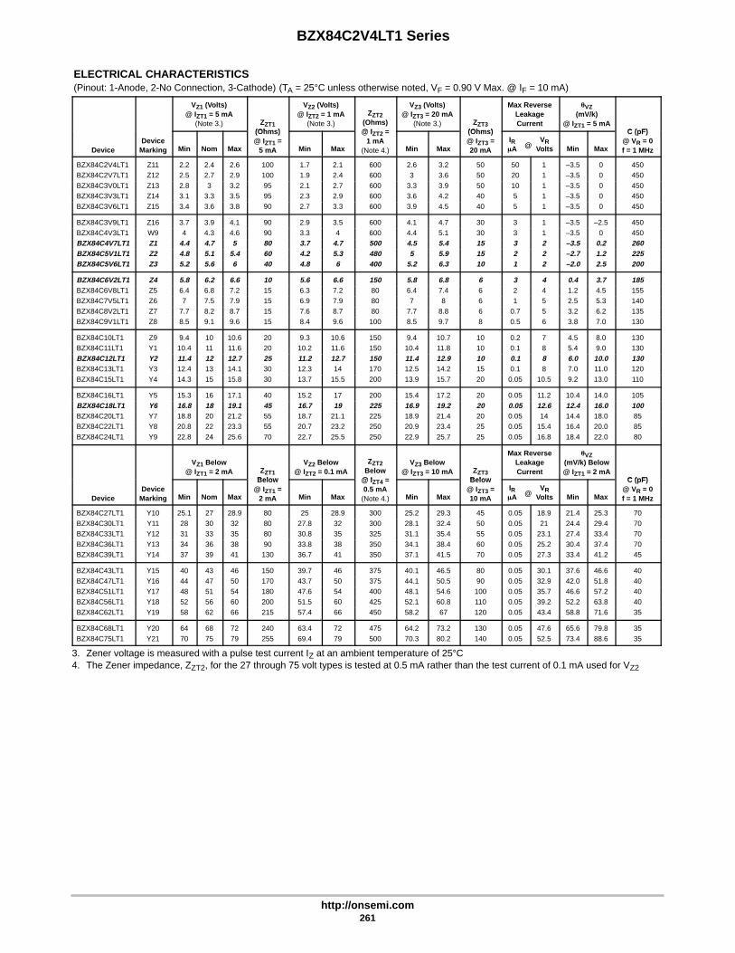
BZX84C2V4LT1 Series
http://onsemi.com261
ELECTRICAL CHARACTERISTICS(Pinout: 1-Anode, 2-No Connection, 3-Cathode) (TA = 25°C unless otherwise noted, VF = 0.90 V Max. @ IF = 10 mA)
VZ1 (Volts)@ IZT1 = 5 mA
(Note 3.) ZZT1(Ohms)
VZ2 (Volts)@ IZT2 = 1 mA
(Note 3.)
ZZT2(Ohms)@ I
VZ3 (Volts)@ IZT3 = 20 mA
(Note 3.) ZZT3(Ohms)
Max ReverseLeakageCurrent
VZ(mV/k)
@ IZT1 = 5 mAC (pF)
DeviceDevice
Marking Min Nom Max
(Ohms)@ IZT1 =
5 mA Min Max
@ IZT2 =1 mA
(Note 4.) Min Max
(Ohms)@ IZT3 =20 mA
VRVolts
IRA @ Min Max
C (pF)@ VR = 0f = 1 MHz
BZX84C2V4LT1 Z11 2.2 2.4 2.6 100 1.7 2.1 600 2.6 3.2 50 50 1 –3.5 0 450BZX84C2V7LT1 Z12 2.5 2.7 2.9 100 1.9 2.4 600 3 3.6 50 20 1 –3.5 0 450
BZX84C3V0LT1 Z13 2.8 3 3.2 95 2.1 2.7 600 3.3 3.9 50 10 1 –3.5 0 450BZX84C3V3LT1 Z14 3.1 3.3 3.5 95 2.3 2.9 600 3.6 4.2 40 5 1 –3.5 0 450
BZX84C3V6LT1 Z15 3.4 3.6 3.8 90 2.7 3.3 600 3.9 4.5 40 5 1 –3.5 0 450
BZX84C3V9LT1 Z16 3.7 3.9 4.1 90 2.9 3.5 600 4.1 4.7 30 3 1 –3.5 –2.5 450
BZX84C4V3LT1 W9 4 4.3 4.6 90 3.3 4 600 4.4 5.1 30 3 1 –3.5 0 450BZX84C4V7LT1 Z1 4.4 4.7 5 80 3.7 4.7 500 4.5 5.4 15 3 2 –3.5 0.2 260BZX84C5V1LT1 Z2 4.8 5.1 5.4 60 4.2 5.3 480 5 5.9 15 2 2 –2.7 1.2 225BZX84C5V6LT1 Z3 5.2 5.6 6 40 4.8 6 400 5.2 6.3 10 1 2 –2.0 2.5 200
BZX84C6V2LT1 Z4 5.8 6.2 6.6 10 5.6 6.6 150 5.8 6.8 6 3 4 0.4 3.7 185BZX84C6V8LT1 Z5 6.4 6.8 7.2 15 6.3 7.2 80 6.4 7.4 6 2 4 1.2 4.5 155BZX84C7V5LT1 Z6 7 7.5 7.9 15 6.9 7.9 80 7 8 6 1 5 2.5 5.3 140
BZX84C8V2LT1 Z7 7.7 8.2 8.7 15 7.6 8.7 80 7.7 8.8 6 0.7 5 3.2 6.2 135BZX84C9V1LT1 Z8 8.5 9.1 9.6 15 8.4 9.6 100 8.5 9.7 8 0.5 6 3.8 7.0 130
BZX84C10LT1 Z9 9.4 10 10.6 20 9.3 10.6 150 9.4 10.7 10 0.2 7 4.5 8.0 130BZX84C11LT1 Y1 10.4 11 11.6 20 10.2 11.6 150 10.4 11.8 10 0.1 8 5.4 9.0 130
BZX84C12LT1 Y2 11.4 12 12.7 25 11.2 12.7 150 11.4 12.9 10 0.1 8 6.0 10.0 130BZX84C13LT1 Y3 12.4 13 14.1 30 12.3 14 170 12.5 14.2 15 0.1 8 7.0 11.0 120
BZX84C15LT1 Y4 14.3 15 15.8 30 13.7 15.5 200 13.9 15.7 20 0.05 10.5 9.2 13.0 110
BZX84C16LT1 Y5 15.3 16 17.1 40 15.2 17 200 15.4 17.2 20 0.05 11.2 10.4 14.0 105
BZX84C18LT1 Y6 16.8 18 19.1 45 16.7 19 225 16.9 19.2 20 0.05 12.6 12.4 16.0 100BZX84C20LT1 Y7 18.8 20 21.2 55 18.7 21.1 225 18.9 21.4 20 0.05 14 14.4 18.0 85BZX84C22LT1 Y8 20.8 22 23.3 55 20.7 23.2 250 20.9 23.4 25 0.05 15.4 16.4 20.0 85
BZX84C24LT1 Y9 22.8 24 25.6 70 22.7 25.5 250 22.9 25.7 25 0.05 16.8 18.4 22.0 80
VZ1 Below@ IZT1 = 2 mA ZZT1
Below
VZ2 Below@ IZT2 = 0.1 mA
ZZT2Below
@ I
VZ3 Below@ IZT3 = 10 mA ZZT3
Below
Max ReverseLeakageCurrent
VZ(mV/k) Below@ IZT1 = 2 mA
C (pF)
DeviceDevice
Marking Min Nom Max
Below@ IZT1 =
2 mA Min Max
@ IZT4 =0.5 mA
(Note 4.) Min Max
Below@ IZT3 =10 mA
VRVolts
IRA @ Min Max
C (pF)@ VR = 0f = 1 MHz
BZX84C27LT1 Y10 25.1 27 28.9 80 25 28.9 300 25.2 29.3 45 0.05 18.9 21.4 25.3 70
BZX84C30LT1 Y11 28 30 32 80 27.8 32 300 28.1 32.4 50 0.05 21 24.4 29.4 70BZX84C33LT1 Y12 31 33 35 80 30.8 35 325 31.1 35.4 55 0.05 23.1 27.4 33.4 70
BZX84C36LT1 Y13 34 36 38 90 33.8 38 350 34.1 38.4 60 0.05 25.2 30.4 37.4 70BZX84C39LT1 Y14 37 39 41 130 36.7 41 350 37.1 41.5 70 0.05 27.3 33.4 41.2 45
BZX84C43LT1 Y15 40 43 46 150 39.7 46 375 40.1 46.5 80 0.05 30.1 37.6 46.6 40BZX84C47LT1 Y16 44 47 50 170 43.7 50 375 44.1 50.5 90 0.05 32.9 42.0 51.8 40
BZX84C51LT1 Y17 48 51 54 180 47.6 54 400 48.1 54.6 100 0.05 35.7 46.6 57.2 40BZX84C56LT1 Y18 52 56 60 200 51.5 60 425 52.1 60.8 110 0.05 39.2 52.2 63.8 40
BZX84C62LT1 Y19 58 62 66 215 57.4 66 450 58.2 67 120 0.05 43.4 58.8 71.6 35
BZX84C68LT1 Y20 64 68 72 240 63.4 72 475 64.2 73.2 130 0.05 47.6 65.6 79.8 35
BZX84C75LT1 Y21 70 75 79 255 69.4 79 500 70.3 80.2 140 0.05 52.5 73.4 88.6 35
3. Zener voltage is measured with a pulse test current IZ at an ambient temperature of 25°C4. The Zener impedance, ZZT2, for the 27 through 75 volt types is tested at 0.5 mA rather than the test current of 0.1 mA used for VZ2

BZX84C2V4LT1 Series
http://onsemi.com262
TYPICAL CHARACTERISTICSV
Z, T
EM
PE
RAT
UR
E C
OE
FF
ICIE
NT
(mV
/C
)°
θ
VZ, NOMINAL ZENER VOLTAGE (V)
-3
-2
-1
0
1
2
3
4
5
6
7
8
12111098765432
Figure 1. Temperature Coefficients(Temperature Range –55 °C to +150°C)
TYPICAL TC VALUES
VZ @ IZT
VZ
, TE
MP
ER
ATU
RE
CO
EF
FIC
IEN
T (m
V/
C)
°θ
100
10
110 100
VZ, NOMINAL ZENER VOLTAGE (V)
Figure 2. Temperature Coefficients(Temperature Range –55 °C to +150°C)
VZ @ IZT
100
VZ, NOMINAL ZENER VOLTAGE
Figure 3. Effect of Zener Voltage onZener Impedance
101
ZZ
T, D
YN
AM
IC IM
PE
DA
NC
E (
)Ω
1000
100
10
1
TJ = 25°C
IZ(AC) = 0.1 IZ(DC)
f = 1 kHzIZ = 1 mA
5 mA
20 mA
VF, FORWARD VOLTAGE (V)
Figure 4. Typical Forward Voltage
1.21.11.00.90.80.70.60.50.4
I F, F
OR
WA
RD
CU
RR
EN
T (m
A)
1000
100
10
1
75 V (MMBZ5267BLT1)
91 V (MMBZ5270BLT1)
150°C 75°C 25°C 0°C
TYPICAL TC VALUES

BZX84C2V4LT1 Series
http://onsemi.com263
TYPICAL CHARACTERISTICSC
, CA
PAC
ITA
NC
E (
pF)
100
VZ, NOMINAL ZENER VOLTAGE (V)
Figure 5. Typical Capacitance
1000
100
10
1101
BIAS AT
50% OF VZ NOM
TA = 25°C0 V BIAS
1 V BIAS
12
VZ, ZENER VOLTAGE (V)
100
10
1
0.1
0.011086420
TA = 25°C
I Z, Z
EN
ER
CU
RR
EN
T (m
A)
VZ, ZENER VOLTAGE (V)
100
10
1
0.1
0.0110 30 50 70 90
TA = 25°CI R
, LE
AK
AG
E C
UR
RE
NT
(A
)µ
90
VZ, NOMINAL ZENER VOLTAGE (V)
Figure 6. Typical Leakage Current
1000
100
10
1
0.1
0.01
0.001
0.0001
0.0000180706050403020100
+150°C
+25°C
-55°C
I Z, Z
EN
ER
CU
RR
EN
T (m
A)
Figure 7. Zener Voltage versus Zener Current(VZ Up to 12 V)
Figure 8. Zener Voltage versus Zener Current(12 V to 91 V)

Semiconductor Components Industries, LLC, 2001
April, 2001 – Rev. 2264 Publication Order Number:
MMBZ5221BLT1/D
MMBZ5221BLT1 Series
Zener Voltage Regulators
225 mW SOT–23 Surface MountThis series of Zener diodes is offered in the convenient, surface
mount plastic SOT–23 package. These devices are designed to providevoltage regulation with minimum space requirement. They are wellsuited for applications such as cellular phones, hand held portables,and high density PC boards.
Specification Features:• 225 mW Rating on FR–4 or FR–5 Board
• Zener Voltage Range – 2.4 V to 91 V
• Package Designed for Optimal Automated Board Assembly
• Small Package Size for High Density Applications
• ESD Rating of Class 3 (>16 KV) per Human Body Model
Mechanical Characteristics:CASE: Void-free, transfer-molded, thermosetting plastic caseFINISH: Corrosion resistant finish, easily solderableMAXIMUM CASE TEMPERATURE FOR SOLDERING PURPOSES:
260°C for 10 SecondsPOLARITY: Cathode indicated by polarity bandFLAMMABILITY RATING: UL94 V–0
MAXIMUM RATINGS
Rating Symbol Max Unit
Total Power Dissipation on FR–5 Board,(Note 1.) @ TA = 25°CDerated above 25°C
PD2251.8
mWmW/°C
Thermal Resistance – Junction to Ambient RJA 556 °C/W
Total Power Dissipation on AluminaSubstrate, (Note 2.) @ TA = 25°CDerated above 25°C
PD3002.4
mWmW/°C
Thermal Resistance – Junction to Ambient RJA 417 °C/W
Junction and StorageTemperature Range
TJ, Tstg –65 to+150
°C
1. FR–5 = 1.0 X 0.75 X 0.62 in.2. Alumina = 0.4 X 0.3 X 0.024 in., 99.5% alumina
Device Package Shipping
ORDERING INFORMATION
SOT–23CASE 318STYLE 8
http://onsemi.com
3Cathode
1Anode
MMBZ52xxBLT1 SOT–23 3000/Tape & Reel
MARKING DIAGRAM
See specific marking information in the device markingcolumn of the Electrical Characteristics table on page 266 ofthis data sheet.
DEVICE MARKING INFORMATION
xxx = Specific Device CodeM = Date Code
xxx
†The “T1” suffix refers to an 8 mm, 7 inch reel.The “T3” suffix refers to an 8 mm, 13 inch reel.
M
MMBZ52xxBLT3 SOT–23 10,000/Tape & Reel
3
12
Devices listed in bold, italic are ON SemiconductorPreferred devices. Preferred devices are recommendedchoices for future use and best overall value.

Zener Voltage Regulator
IF
V
I
IRIZT
VRVZVF
MMBZ5221BLT1 Series
http://onsemi.com265
ELECTRICAL CHARACTERISTICS(Pinout: 1-Anode, 2-No Connection, 3-Cathode) (TA = 25°Cunless otherwise noted, VF = 0.95 V Max. @ IF = 10 mA)
Symbol Parameter
VZ Reverse Zener Voltage @ IZT
IZT Reverse Current
ZZT Maximum Zener Impedance @ IZT
IZK Reverse Current
ZZK Maximum Zener Impedance @ IZK
IR Reverse Leakage Current @ VR
VR Reverse Voltage
IF Forward Current
VF Forward Voltage @ IF

MMBZ5221BLT1 Series
http://onsemi.com266
ELECTRICAL CHARACTERISTICS (Pinout: 1-Anode, 2-NC, 3-Cathode) (VF = 0.9 V Max @ IF = 10 mA for all types.)
Zener Voltage (Note 3.) Zener Impedance Leakage Current
DeviceVZ (Volts) @ IZT ZZT @ IZT ZZK @ IZK IR @ VR
DeviceDevice
Marking Min Nom Max mA mA A Volts
MMBZ5221BLT1 18A 2.28 2.4 2.52 20 30 1200 0.25 100 1MMBZ5222BLT1 18B 2.37 2.5 2.63 20 30 1250 0.25 100 1MMBZ5223BLT1 18C 2.56 2.7 2.84 20 30 1300 0.25 75 1MMBZ5224BLT1 18D 2.66 2.8 2.94 20 30 1400 0.25 75 1MMBZ5225BLT1 18E 2.85 3 3.15 20 29 1600 0.25 50 1
MMBZ5226BLT1 8A 3.13 3.3 3.47 20 28 1600 0.25 25 1MMBZ5227BLT1 8B 3.42 3.6 3.78 20 24 1700 0.25 15 1MMBZ5228BLT1 8C 3.70 3.9 4.10 20 23 1900 0.25 10 1MMBZ5229BLT1 8D 4.08 4.3 4.52 20 22 2000 0.25 5 1MMBZ5230BLT1 8E 4.46 4.7 4.94 20 19 1900 0.25 5 2
MMBZ5231BLT1 8F 4.84 5.1 5.36 20 17 1600 0.25 5 2MMBZ5232BLT1 8G 5.32 5.6 5.88 20 11 1600 0.25 5 3MMBZ5233BLT1 8H 5.70 6 6.30 20 7 1600 0.25 5 3.5MMBZ5234BLT1 8J 5.89 6.2 6.51 20 7 1000 0.25 5 4MMBZ5235BLT1 8K 6.46 6.8 7.14 20 5 750 0.25 3 5
MMBZ5236BLT1 8L 7.12 7.5 7.88 20 6 500 0.25 3 6MMBZ5237BLT1 8M 7.79 8.2 8.61 20 8 500 0.25 3 6.5MMBZ5238BLT1 8N 8.26 8.7 9.14 20 8 600 0.25 3 6.5MMBZ5239BLT1 8P 8.64 9.1 9.56 20 10 600 0.25 3 7MMBZ5240BLT1 8Q 9.50 10 10.50 20 17 600 0.25 3 8
MMBZ5241BLT1 8R 10.4 11 11.55 20 22 600 0.25 2 8.4MMBZ5242BLT1 8S 11.40 12 12.60 20 30 600 0.25 1 9.1MMBZ5243BLT1 8T 12.35 13 13.65 9.5 13 600 0.25 0.5 9.9MMBZ5244BLT1 8U 13.30 14 14.70 9 15 600 0.25 0.1 10MMBZ5245BLT1 8V 14.25 15 15.75 8.5 16 600 0.25 0.1 11
MMBZ5246BLT1 8W 15.20 16 16.80 7.8 17 600 0.25 0.1 12MMBZ5247BLT1 8X 16.15 17 17.85 7.4 19 600 0.25 0.1 13MMBZ5248BLT1 8Y 17.10 18 18.90 7 21 600 0.25 0.1 14MMBZ5249BLT1 8Z 18.05 19 19.95 6.6 23 600 0.25 0.1 14MMBZ5250BLT1 81A 19.00 20 21.00 6.2 25 600 0.25 0.1 15
MMBZ5251BLT1 81B 20.90 22 23.10 5.6 29 600 0.25 0.1 17MMBZ5252BLT1 81C 22.80 24 25.20 5.2 33 600 0.25 0.1 18MMBZ5253BLT1 81D 23.75 25 26.25 5 35 600 0.25 0.1 19MMBZ5254BLT1 81E 25.65 27 28.35 4.6 41 600 0.25 0.1 21MMBZ5255BLT1 81F 26.60 28 29.40 4.5 44 600 0.25 0.1 21
MMBZ5256BLT1 81G 28.50 30 31.50 4.2 49 600 0.25 0.1 23MMBZ5257BLT1 81H 31.35 33 34.65 3.8 58 700 0.25 0.1 25MMBZ5258BLT1 81J 34.20 36 37.80 3.4 70 700 0.25 0.1 27MMBZ5259BLT1 81K 37.05 39 40.95 3.2 80 800 0.25 0.1 30MMBZ5260BLT1 81L 40.85 43 45.15 3 93 900 0.25 0.1 33
MMBZ5261BLT1 81M 44.65 47 49.35 2.7 105 1000 0.25 0.1 36MMBZ5262BLT1 81N 48.45 51 53.55 2.5 125 1100 0.25 0.1 39MMBZ5263BLT1 81P 53.20 56 58.80 2.2 150 1300 0.25 0.1 43MMBZ5264BLT1 81Q 57.00 60 63.00 2.1 170 1400 0.25 0.1 46MMBZ5265BLT1 81R 58.90 62 65.10 2 185 1400 0.25 0.1 47
MMBZ5266BLT1 81S 64.60 68 71.40 1.8 230 1600 0.25 0.1 52MMBZ5267BLT1 81T 71.25 75 78.75 1.7 270 1700 0.25 0.1 56MMBZ5268BLT1 81U 77.90 82 86.10 1.5 330 2000 0.25 0.1 62MMBZ5269BLT1 81V 82.65 87 91.35 1.4 370 2200 0.25 0.1 68MMBZ5270BLT1 81W 86.45 91 95.55 1.4 400 2300 0.25 0.1 69
3. Zener voltage is measured with a pulse test current IZ at an ambient temperature of 25°C
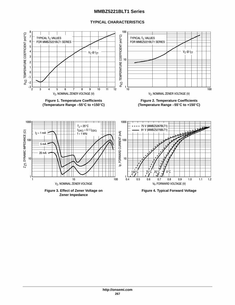
MMBZ5221BLT1 Series
http://onsemi.com267
TYPICAL CHARACTERISTICSV
Z, T
EM
PE
RAT
UR
E C
OE
FF
ICIE
NT
(mV
/C
)°
θ
VZ, NOMINAL ZENER VOLTAGE (V)
-3
-2
-1
0
1
2
3
4
5
6
7
8
12111098765432
Figure 1. Temperature Coefficients(Temperature Range –55 °C to +150°C)
TYPICAL TC VALUES
FOR MMBZ5221BLT1 SERIES
VZ @ IZT
VZ
, TE
MP
ER
ATU
RE
CO
EF
FIC
IEN
T (m
V/
C)
°θ
100
10
110 100
VZ, NOMINAL ZENER VOLTAGE (V)
Figure 2. Temperature Coefficients(Temperature Range –55 °C to +150°C)
TYPICAL TC VALUES
FOR MMBZ5221BLT1 SERIES
VZ @ IZT
100
VZ, NOMINAL ZENER VOLTAGE
Figure 3. Effect of Zener Voltage onZener Impedance
101
ZZ
T, D
YN
AM
IC IM
PE
DA
NC
E (
)Ω
1000
100
10
1
TJ = 25°C
IZ(AC) = 0.1 IZ(DC)
f = 1 kHzIZ = 1 mA
5 mA
20 mA
VF, FORWARD VOLTAGE (V)
Figure 4. Typical Forward Voltage
1.21.11.00.90.80.70.60.50.4
I F, F
OR
WA
RD
CU
RR
EN
T (m
A)
1000
100
10
1
75 V (MMBZ5267BLT1)
91 V (MMBZ5270BLT1)
150°C 75°C 25°C 0°C

MMBZ5221BLT1 Series
http://onsemi.com268
TYPICAL CHARACTERISTICSC
, CA
PAC
ITA
NC
E (
pF)
100
VZ, NOMINAL ZENER VOLTAGE (V)
Figure 5. Typical Capacitance
1000
100
10
1101
BIAS AT
50% OF VZ NOM
TA = 25°C0 V BIAS
1 V BIAS
12
VZ, ZENER VOLTAGE (V)
100
10
1
0.1
0.011086420
TA = 25°C
I Z, Z
EN
ER
CU
RR
EN
T (m
A)
VZ, ZENER VOLTAGE (V)
100
10
1
0.1
0.0110 30 50 70 90
TA = 25°CI R
, LE
AK
AG
E C
UR
RE
NT
(A
)µ
90
VZ, NOMINAL ZENER VOLTAGE (V)
Figure 6. Typical Leakage Current
1000
100
10
1
0.1
0.01
0.001
0.0001
0.0000180706050403020100
+150°C
+25°C
-55°C
I Z, Z
EN
ER
CU
RR
EN
T (m
A)
Figure 7. Zener Voltage versus Zener Current(VZ Up to 12 V)
Figure 8. Zener Voltage versus Zener Current(12 V to 91 V)

Semiconductor Components Industries, LLC, 2001
May, 2001 – Rev. 1269 Publication Order Number:
MMSZ5221BT1/D
MMSZ5221BT1 Series
Zener Voltage Regulators
500 mW SOD–123 Surface MountThree complete series of Zener diodes are offered in the convenient,
surface mount plastic SOD–123 package. These devices provide aconvenient alternative to the leadless 34–package style.
Specification Features:• 500 mW Rating on FR–4 or FR–5 Board
• Wide Zener Reverse Voltage Range – 2.4 V to 110 V
• Package Designed for Optimal Automated Board Assembly
• Small Package Size for High Density Applications
• General Purpose, Medium Current
• ESD Rating of Class 3 (>16 KV) per Human Body Model
Mechanical Characteristics:CASE: Void-free, transfer-molded, thermosetting plastic caseFINISH: Corrosion resistant finish, easily solderableMAXIMUM CASE TEMPERATURE FOR SOLDERING PURPOSES:
260°C for 10 SecondsPOLARITY: Cathode indicated by polarity bandFLAMMABILITY RATING: UL94 V–0
MAXIMUM RATINGS
Rating Symbol Max Unit
Total Power Dissipation on FR–5 Board,(Note 1.) @ TL = 75°CDerated above 75°C
PD5006.7
mWmW/°C
Thermal Resistance –Junction to Ambient (Note 2.)
RJA 340 °C/W
Thermal Resistance –Junction to Lead (Note 2.)
RJL 150 °C/W
Junction and StorageTemperature Range
TJ, Tstg –55 to+150
°C
1. FR–5 = 3.5 X 1.5 inches, using the On minimum recommended footprint asshown in Figure NO TAG
2. Thermal Resistance measurement obtained via infrared Scan Method
Device Package Shipping
ORDERING INFORMATION
SOD–123CASE 425STYLE 1
http://onsemi.com
1Cathode
2Anode
MMSZ52xxBT1 SOD–123 3000/Tape & Reel
MARKING DIAGRAM
See specific marking information in the device markingcolumn of the Electrical Characteristics table on page 271 ofthis data sheet.
DEVICE MARKING INFORMATION
xx = Specific Device CodeM = Date Code
xx M
†The “T1” suffix refers to an 8 mm, 7 inch reel.The “T3” suffix refers to an 8 mm, 13 inch reel.
1
2
Devices listed in bold, italic are ON SemiconductorPreferred devices. Preferred devices are recommendedchoices for future use and best overall value.
ÂÂÂÂÂÂ
MMSZ52xxBT3 SOD–123 10,000/Tape & Reel

Zener Voltage Regulator
IF
V
I
IRIZT
VRVZVF
MMSZ5221BT1 Series
http://onsemi.com270
ELECTRICAL CHARACTERISTICS (TA = 25°C unlessotherwise noted, VF = 0.95 V Max. @ IF = 10 mA)
Symbol Parameter
VZ Reverse Zener Voltage @ IZT
IZT Reverse Current
ZZT Maximum Zener Impedance @ IZT
IZK Reverse Current
ZZK Maximum Zener Impedance @ IZK
IR Reverse Leakage Current @ VR
VR Reverse Voltage
IF Forward Current
VF Forward Voltage @ IF

MMSZ5221BT1 Series
http://onsemi.com271
ELECTRICAL CHARACTERISTICS (TA = 25°C unless otherwise noted, VF = 0.9 V Max. @ IF = 10 mA)
Zener Voltage (Notes 3. and 4.) Zener Impedance (Note 5.) Leakage Current
DeviceVZ (Volts) @ IZT ZZT @ IZT ZZK @ IZK IR @ VR
DeviceDevice
Marking Min Nom Max mA mA A Volts
MMSZ5221BT1 C1 2.28 2.4 2.52 20 30 1200 0.25 100 1MMSZ5222BT1 C2 2.38 2.5 2.63 20 30 1250 0.25 100 1MMSZ5223BT1 C3 2.57 2.7 2.84 20 30 1300 0.25 75 1MMSZ5224BT1 C4 2.66 2.8 2.94 20 30 1400 0.25 75 1MMSZ5225BT1 C5 2.85 3.0 3.15 20 29 1600 0.25 50 1
MMSZ5226BT1 D1 3.14 3.3 3.47 20 28 1600 0.25 25 1MMSZ5227BT1 D2 3.42 3.6 3.78 20 24 1700 0.25 15 1MMSZ5228BT1 D3 3.71 3.9 4.10 20 23 1900 0.25 10 1MMSZ5229BT1 D4 4.09 4.3 4.52 20 22 2000 0.25 5 1MMSZ5230BT1 D5 4.47 4.7 4.94 20 19 1900 0.25 5 2
MMSZ5231BT1 E1 4.85 5.1 5.36 20 17 1600 0.25 5 2MMSZ5232BT1 E2 5.32 5.6 5.88 20 11 1600 0.25 5 3MMSZ5233BT1 E3 5.70 6.0 6.30 20 7 1600 0.25 5 3.5MMSZ5234BT1 E4 5.89 6.2 6.51 20 7 1000 0.25 5 4MMSZ5235BT1 E5 6.46 6.8 7.14 20 5 750 0.25 3 5
MMSZ5236BT1 F1 7.13 7.5 7.88 20 6 500 0.25 3 6MMSZ5237BT1 F2 7.79 8.2 8.61 20 8 500 0.25 3 6.5MMSZ5238BT1 F3 8.27 8.7 9.14 20 8 600 0.25 3 6.5MMSZ5239BT1 F4 8.65 9.1 9.56 20 10 600 0.25 3 7MMSZ5240BT1 F5 9.50 10 10.50 20 17 600 0.25 3 8
MMSZ5241BT1 H1 10.45 11 11.55 20 22 600 0.25 2 8.4MMSZ5242BT1 H2 11.40 12 12.60 20 30 600 0.25 1 9.1MMSZ5243BT1 H3 12.35 13 13.65 9.5 13 600 0.25 0.5 9.9MMSZ5244BT1 H4 13.30 14 14.70 9.0 15 600 0.25 0.1 10MMSZ5245BT1 H5 14.25 15 15.75 8.5 16 600 0.25 0.1 11
MMSZ5246BT1 J1 15.20 16 16.80 7.8 17 600 0.25 0.1 12MMSZ5247BT1 J2 16.15 17 17.85 7.4 19 600 0.25 0.1 13MMSZ5248BT1 J3 17.10 18 18.90 7.0 21 600 0.25 0.1 14MMSZ5249BT1 J4 18.05 19 19.95 6.6 23 600 0.25 0.1 14MMSZ5250BT1 J5 19.00 20 21.00 6.2 25 600 0.25 0.1 15
MMSZ5251BT1 K1 20.90 22 23.10 5.6 29 600 0.25 0.1 17MMSZ5252BT1 K2 22.80 24 25.20 5.2 33 600 0.25 0.1 18MMSZ5253BT1 K3 23.75 25 26.25 5.0 35 600 0.25 0.1 19MMSZ5254BT1 K4 25.65 27 28.35 4.6 41 600 0.25 0.1 21MMSZ5255BT1 K5 26.60 28 29.40 4.5 44 600 0.25 0.1 21
MMSZ5256BT1 M1 28.50 30 31.50 4.2 49 600 0.25 0.1 23MMSZ5257BT1 M2 31.35 33 34.65 3.8 58 700 0.25 0.1 25MMSZ5258BT1 M3 34.20 36 37.80 3.4 70 700 0.25 0.1 27MMSZ5259BT1 M4 37.05 39 40.95 3.2 80 800 0.25 0.1 30MMSZ5260BT1 M5 40.85 43 45.15 3.0 93 900 0.25 0.1 33
MMSZ5261BT1 N1 44.65 47 49.35 2.7 105 1000 0.25 0.1 36MMSZ5262BT1 N2 48.45 51 53.55 2.5 125 1100 0.25 0.1 39MMSZ5263BT1 N3 53.20 56 58.80 2.2 150 1300 0.25 0.1 43MMSZ5264BT1 N4 57.00 60 63.00 2.1 170 1400 0.25 0.1 46MMSZ5265BT1 N5 58.90 62 65.10 2.0 185 1400 0.25 0.1 47
MMSZ5266BT1 P1 64.60 68 71.40 1.8 230 1600 0.25 0.1 52MMSZ5267BT1 P2 71.25 75 78.75 1.7 270 1700 0.25 0.1 56MMSZ5268BT1 P3 77.90 82 86.10 1.5 330 2000 0.25 0.1 62MMSZ5269BT1 P4 82.65 87 91.35 1.4 370 2200 0.25 0.1 68MMSZ5270BT1 P5 86.45 91 95.55 1.4 400 2300 0.25 0.1 69
MMSZ5272BT1 R2 104.5 110 115.5 1.1 750 3000 0.25 0.1 84
3. The type numbers shown have a standard tolerance of ±5% on the nominal Zener voltage.4. Nominal Zener voltage is measured with the device junction in thermal equilibrium at TL = 30°C ±1°C5. ZZT and ZZK are measured by dividing the AC voltage drop across the device by the ac current applied.
The specified limits are for IZ(AC) = 0.1 IZ(dc) with the AC frequency = 1 KHz.

MMSZ5221BT1 Series
http://onsemi.com272
TYPICAL CHARACTERISTICSV
Z, T
EM
PE
RAT
UR
E C
OE
FF
ICIE
NT
(mV
/C
)°
θ
VZ, NOMINAL ZENER VOLTAGE (V)
-3
-2
-1
0
1
2
3
4
5
6
7
8
12111098765432
Figure 1. Temperature Coefficients(Temperature Range –55 °C to +150°C)
TYPICAL TC VALUES
FOR MMSZ5221BT1 SERIES
VZ @ IZT
VZ
, TE
MP
ER
ATU
RE
CO
EF
FIC
IEN
T (m
V/
C)
°θ
100
10
110 100
VZ, NOMINAL ZENER VOLTAGE (V)
Figure 2. Temperature Coefficients(Temperature Range –55 °C to +150°C)
VZ @ IZT
1.2
1.0
0.8
0.6
0.4
0.2
01501251007550250
T, TEMPERATURE (°C)
Figure 3. Steady State Power Derating
PD versus TA
PD versus TL
P pk
, PE
AK
SU
RG
E P
OW
ER
(W
AT
TS
)
0.1
PW, PULSE WIDTH (ms)
Figure 4. Maximum Nonrepetitive Surge Power
1 10 100 1000
1000
100
10
1
RECTANGULAR
WAVEFORM, TA = 25°C
100
VZ, NOMINAL ZENER VOLTAGE
Figure 5. Effect of Zener Voltage onZener Impedance
101
ZZ
T, D
YN
AM
IC IM
PE
DA
NC
E (
)Ω
1000
100
10
1
TJ = 25°C
IZ(AC) = 0.1 IZ(DC)
f = 1 kHzIZ = 1 mA
5 mA
20 mA
VF, FORWARD VOLTAGE (V)
Figure 6. Typical Forward Voltage
1.21.11.00.90.80.70.60.50.4
I F, F
OR
WA
RD
CU
RR
EN
T (m
A)
1000
100
10
1
75 V (MMSZ5267BT1)
91 V (MMSZ5270BT1)
150°C 75°C 25°C 0°C
TYPICAL TC VALUES
FOR MMSZ5221BT1 SERIES

MMSZ5221BT1 Series
http://onsemi.com273
TYPICAL CHARACTERISTICSC
, CA
PAC
ITA
NC
E (
pF)
100
VZ, NOMINAL ZENER VOLTAGE (V)
Figure 7. Typical Capacitance
1000
100
10
1101
BIAS AT
50% OF VZ NOM
TA = 25°C0 V BIAS
1 V BIAS
12
VZ, ZENER VOLTAGE (V)
100
10
1
0.1
0.011086420
TA = 25°C
I Z, Z
EN
ER
CU
RR
EN
T (m
A)
VZ, ZENER VOLTAGE (V)
100
10
1
0.1
0.0110 30 50 70 90
TA = 25°CI R
, LE
AK
AG
E C
UR
RE
NT
(A
)µ
90
VZ, NOMINAL ZENER VOLTAGE (V)
Figure 8. Typical Leakage Current
1000
100
10
1
0.1
0.01
0.001
0.0001
0.0000180706050403020100
+150°C
+25°C
-55°C
I Z, Z
EN
ER
CU
RR
EN
T (m
A)
Figure 9. Zener Voltage versus Zener Current(VZ Up to 12 V)
Figure 10. Zener Voltage versus Zener Current(12 V to 91 V)

Semiconductor Components Industries, LLC, 2001
May, 2001 – Rev. 1274 Publication Order Number:
MMSZ4678T1/D
MMSZ4678T1 Series
Zener Voltage Regulators
500 mW SOD–123 Surface MountThree complete series of Zener diodes are offered in the convenient,
surface mount plastic SOD–123 package. These devices provide aconvenient alternative to the leadless 34–package style.
Specification Features:• 500 mW Rating on FR–4 or FR–5 Board
• Wide Zener Reverse Voltage Range – 1.8 V to 43 V
• Package Designed for Optimal Automated Board Assembly
• Small Package Size for High Density Applications
• ESD Rating of Class 3 (>16 KV) per Human Body Model
Mechanical Characteristics:CASE: Void-free, transfer-molded, thermosetting plastic caseFINISH: Corrosion resistant finish, easily solderableMAXIMUM CASE TEMPERATURE FOR SOLDERING PURPOSES:
260°C for 10 SecondsPOLARITY: Cathode indicated by polarity bandFLAMMABILITY RATING: UL94 V–0
MAXIMUM RATINGS
Rating Symbol Max Unit
Total Power Dissipation on FR–5 Board,(Note 1.) @ TL = 75°CDerated above 75°C
PD5006.7
mWmW/°C
Thermal Resistance –Junction to Ambient (Note 2.)
RJA 340 °C/W
Thermal Resistance –Junction to Lead (Note 2.)
RJL 150 °C/W
Junction and StorageTemperature Range
TJ, Tstg –55 to+150
°C
1. FR–5 = 3.5 X 1.5 inches, using the On minimum recommended footprint asshown in Figure NO TAG
2. Thermal Resistance measurement obtained via infrared Scan Method
Device Package Shipping
ORDERING INFORMATION
SOD–123CASE 425STYLE 1
http://onsemi.com
1Cathode
2Anode
MMSZ4xxxT1 SOD–123 3000/Tape & Reel
MARKING DIAGRAM
See specific marking information in the device markingcolumn of the Electrical Characteristics table on page 276 ofthis data sheet.
DEVICE MARKING INFORMATION
xx = Specific Device CodeM = Date Code
xx M
†The “T1” suffix refers to an 8 mm, 7 inch reel.The “T3” suffix refers to an 8 mm, 13 inch reel.
1
2
Devices listed in bold, italic are ON SemiconductorPreferred devices. Preferred devices are recommendedchoices for future use and best overall value.
ÂÂÂÂÂÂ
MMSZ4xxxT3 SOD–123 10,000/Tape & Reel

Zener Voltage Regulator
IF
V
I
IRIZT
VRVZVF
MMSZ4678T1 Series
http://onsemi.com275
ELECTRICAL CHARACTERISTICS (TA = 25°C unlessotherwise noted, VF = 0.95 V Max. @ IF = 10 mA)
Symbol Parameter
VZ Reverse Zener Voltage @ IZT
IZT Reverse Current
IR Reverse Leakage Current @ VR
VR Reverse Voltage
IF Forward Current
VF Forward Voltage @ IF
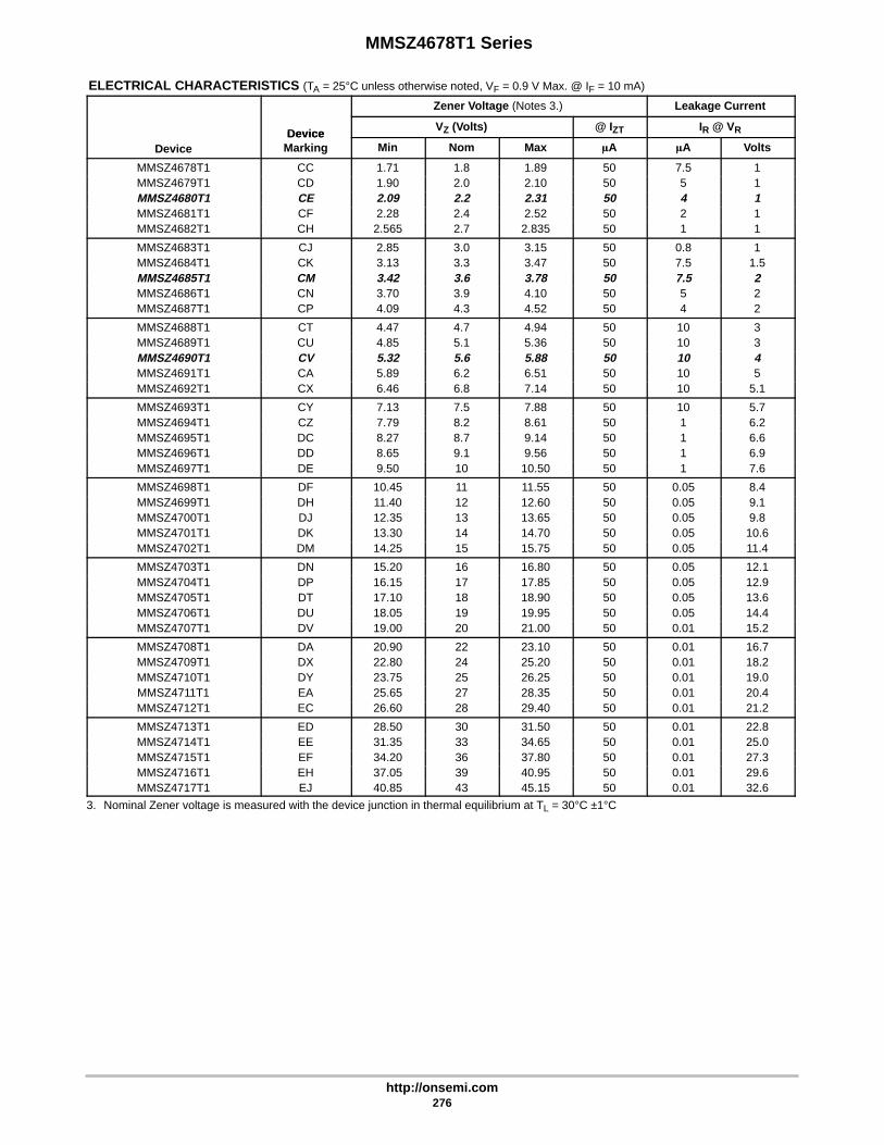
MMSZ4678T1 Series
http://onsemi.com276
ELECTRICAL CHARACTERISTICS (TA = 25°C unless otherwise noted, VF = 0.9 V Max. @ IF = 10 mA)
Zener Voltage (Notes 3.) Leakage Current
DeviceVZ (Volts) @ IZT IR @ VR
DeviceDevice
Marking Min Nom Max A A Volts
MMSZ4678T1 CC 1.71 1.8 1.89 50 7.5 1MMSZ4679T1 CD 1.90 2.0 2.10 50 5 1MMSZ4680T1 CE 2.09 2.2 2.31 50 4 1MMSZ4681T1 CF 2.28 2.4 2.52 50 2 1MMSZ4682T1 CH 2.565 2.7 2.835 50 1 1
MMSZ4683T1 CJ 2.85 3.0 3.15 50 0.8 1MMSZ4684T1 CK 3.13 3.3 3.47 50 7.5 1.5MMSZ4685T1 CM 3.42 3.6 3.78 50 7.5 2MMSZ4686T1 CN 3.70 3.9 4.10 50 5 2MMSZ4687T1 CP 4.09 4.3 4.52 50 4 2
MMSZ4688T1 CT 4.47 4.7 4.94 50 10 3MMSZ4689T1 CU 4.85 5.1 5.36 50 10 3MMSZ4690T1 CV 5.32 5.6 5.88 50 10 4MMSZ4691T1 CA 5.89 6.2 6.51 50 10 5MMSZ4692T1 CX 6.46 6.8 7.14 50 10 5.1
MMSZ4693T1 CY 7.13 7.5 7.88 50 10 5.7MMSZ4694T1 CZ 7.79 8.2 8.61 50 1 6.2MMSZ4695T1 DC 8.27 8.7 9.14 50 1 6.6MMSZ4696T1 DD 8.65 9.1 9.56 50 1 6.9MMSZ4697T1 DE 9.50 10 10.50 50 1 7.6
MMSZ4698T1 DF 10.45 11 11.55 50 0.05 8.4MMSZ4699T1 DH 11.40 12 12.60 50 0.05 9.1MMSZ4700T1 DJ 12.35 13 13.65 50 0.05 9.8MMSZ4701T1 DK 13.30 14 14.70 50 0.05 10.6MMSZ4702T1 DM 14.25 15 15.75 50 0.05 11.4
MMSZ4703T1 DN 15.20 16 16.80 50 0.05 12.1MMSZ4704T1 DP 16.15 17 17.85 50 0.05 12.9MMSZ4705T1 DT 17.10 18 18.90 50 0.05 13.6MMSZ4706T1 DU 18.05 19 19.95 50 0.05 14.4MMSZ4707T1 DV 19.00 20 21.00 50 0.01 15.2
MMSZ4708T1 DA 20.90 22 23.10 50 0.01 16.7MMSZ4709T1 DX 22.80 24 25.20 50 0.01 18.2MMSZ4710T1 DY 23.75 25 26.25 50 0.01 19.0MMSZ4711T1 EA 25.65 27 28.35 50 0.01 20.4MMSZ4712T1 EC 26.60 28 29.40 50 0.01 21.2
MMSZ4713T1 ED 28.50 30 31.50 50 0.01 22.8MMSZ4714T1 EE 31.35 33 34.65 50 0.01 25.0MMSZ4715T1 EF 34.20 36 37.80 50 0.01 27.3MMSZ4716T1 EH 37.05 39 40.95 50 0.01 29.6MMSZ4717T1 EJ 40.85 43 45.15 50 0.01 32.6
3. Nominal Zener voltage is measured with the device junction in thermal equilibrium at TL = 30°C ±1°C
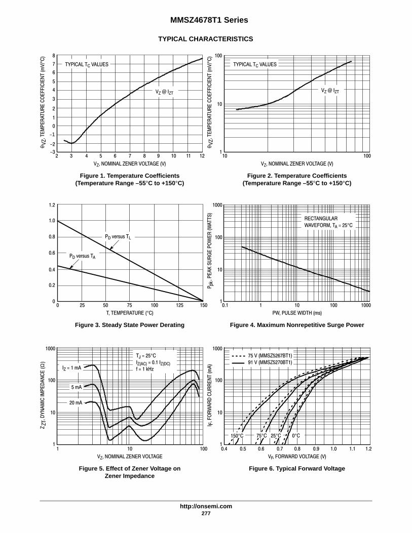
MMSZ4678T1 Series
http://onsemi.com277
TYPICAL CHARACTERISTICSV
Z, T
EM
PE
RAT
UR
E C
OE
FF
ICIE
NT
(mV
/C
)°
θ
VZ, NOMINAL ZENER VOLTAGE (V)
-3
-2
-1
0
1
2
3
4
5
6
7
8
12111098765432
Figure 1. Temperature Coefficients(Temperature Range –55 °C to +150°C)
TYPICAL TC VALUES
VZ @ IZT
VZ
, TE
MP
ER
ATU
RE
CO
EF
FIC
IEN
T (m
V/
C)
°θ
100
10
110 100
VZ, NOMINAL ZENER VOLTAGE (V)
Figure 2. Temperature Coefficients(Temperature Range –55 °C to +150°C)
VZ @ IZT
1.2
1.0
0.8
0.6
0.4
0.2
01501251007550250
T, TEMPERATURE (°C)
Figure 3. Steady State Power Derating
PD versus TA
PD versus TL
P pk
, PE
AK
SU
RG
E P
OW
ER
(W
AT
TS
)
0.1
PW, PULSE WIDTH (ms)
Figure 4. Maximum Nonrepetitive Surge Power
1 10 100 1000
1000
100
10
1
RECTANGULAR
WAVEFORM, TA = 25°C
100
VZ, NOMINAL ZENER VOLTAGE
Figure 5. Effect of Zener Voltage onZener Impedance
101
ZZ
T, D
YN
AM
IC IM
PE
DA
NC
E (
)Ω
1000
100
10
1
TJ = 25°C
IZ(AC) = 0.1 IZ(DC)
f = 1 kHzIZ = 1 mA
5 mA
20 mA
VF, FORWARD VOLTAGE (V)
Figure 6. Typical Forward Voltage
1.21.11.00.90.80.70.60.50.4
I F, F
OR
WA
RD
CU
RR
EN
T (m
A)
1000
100
10
1
75 V (MMSZ5267BT1)
91 V (MMSZ5270BT1)
150°C 75°C 25°C 0°C
TYPICAL TC VALUES

MMSZ4678T1 Series
http://onsemi.com278
TYPICAL CHARACTERISTICSC
, CA
PAC
ITA
NC
E (
pF)
100
VZ, NOMINAL ZENER VOLTAGE (V)
Figure 7. Typical Capacitance
1000
100
10
1101
BIAS AT
50% OF VZ NOM
TA = 25°C0 V BIAS
1 V BIAS
12
VZ, ZENER VOLTAGE (V)
100
10
1
0.1
0.011086420
TA = 25°C
I Z, Z
EN
ER
CU
RR
EN
T (m
A)
VZ, ZENER VOLTAGE (V)
100
10
1
0.1
0.0110 30 50 70 90
TA = 25°CI R
, LE
AK
AG
E C
UR
RE
NT
(A
)µ
90
VZ, NOMINAL ZENER VOLTAGE (V)
Figure 8. Typical Leakage Current
1000
100
10
1
0.1
0.01
0.001
0.0001
0.0000180706050403020100
+150°C
+25°C
-55°C
I Z, Z
EN
ER
CU
RR
EN
T (m
A)
Figure 9. Zener Voltage versus Zener Current(VZ Up to 12 V)
Figure 10. Zener Voltage versus Zener Current(12 V to 91 V)

Semiconductor Components Industries, LLC, 2001
May, 2001 – Rev. 1279 Publication Order Number:
MMSZ2V4T1/D
MMSZ2V4T1 Series
Zener Voltage Regulators
500 mW SOD–123 Surface MountThree complete series of Zener diodes are offered in the convenient,
surface mount plastic SOD–123 package. These devices provide aconvenient alternative to the leadless 34–package style.
Specification Features:• 500 mW Rating on FR–4 or FR–5 Board
• Wide Zener Reverse Voltage Range – 2.4 V to 56 V
• Package Designed for Optimal Automated Board Assembly
• Small Package Size for High Density Applications
• ESD Rating of Class 3 (>16 KV) per Human Body Model
Mechanical Characteristics:CASE: Void-free, transfer-molded, thermosetting plastic caseFINISH: Corrosion resistant finish, easily solderableMAXIMUM CASE TEMPERATURE FOR SOLDERING PURPOSES:
260°C for 10 SecondsPOLARITY: Cathode indicated by polarity bandFLAMMABILITY RATING: UL94 V–0
MAXIMUM RATINGS
Rating Symbol Max Unit
Total Power Dissipation on FR–5 Board,(Note 1.) @ TL = 75°CDerated above 75°C
PD5006.7
mWmW/°C
Thermal Resistance –Junction to Ambient (Note 2.)
RJA 340 °C/W
Thermal Resistance –Junction to Lead (Note 2.)
RJL 150 °C/W
Junction and StorageTemperature Range
TJ, Tstg –55 to+150
°C
1. FR–5 = 3.5 X 1.5 inches, using the On minimum recommended footprint asshown in Figure NO TAG
2. Thermal Resistance measurement obtained via infrared Scan Method
Device Package Shipping
ORDERING INFORMATION
SOD–123CASE 425STYLE 1
http://onsemi.com
1Cathode
2Anode
MMSZxxxT1 SOD–123 3000/Tape & Reel
MARKING DIAGRAM
See specific marking information in the device markingcolumn of the Electrical Characteristics table on page 280 ofthis data sheet.
DEVICE MARKING INFORMATION
xx = Specific Device CodeM = Date Code
xx M
†The “T1” suffix refers to an 8 mm, 7 inch reel.The “T3” suffix refers to an 8 mm, 13 inch reel.
1
2
Devices listed in bold, italic are ON SemiconductorPreferred devices. Preferred devices are recommendedchoices for future use and best overall value.
ÂÂÂÂÂÂ
MMSZxxxT3 SOD–123 10,000/Tape & Reel

Zener Voltage Regulator
IF
V
I
IRIZT
VRVZVF
MMSZ2V4T1 Series
http://onsemi.com280
ELECTRICAL CHARACTERISTICS (TA = 25°C unlessotherwise noted, VF = 0.95 V Max. @ IF = 10 mA)
Symbol Parameter
VZ Reverse Zener Voltage @ IZT
IZT Reverse Current
ZZT Maximum Zener Impedance @ IZT
IR Reverse Leakage Current @ VR
VR Reverse Voltage
IF Forward Current
VF Forward Voltage @ IF
ELECTRICAL CHARACTERISTICS (TA = 25°C unless otherwise noted, VF = 0.9 V Max. @ IF = 10 mA)
VZ1 (Volts)(Notes 3. and 4.)
ZZT1(Note 5.)
VZ2 (Volts)(Notes 3. and 4.)
ZZT2(Note 5.) Leakage Current
Device@ IZT1 = 5 mA @ IZT2 = 1 mA IR @ VR
DeviceDevice
Marking Min Nom Max Min Max A Volts
MMSZ2V4T1 T1 2.28 2.4 2.52 100 1.7 2.1 600 50 1MMSZ2V7T1 T2 2.57 2.7 2.84 100 1.9 2.4 600 20 1MMSZ3V0T1 T3 2.85 3.0 3.15 95 2.1 2.7 600 10 1MMSZ3V3T1 T4 3.14 3.3 3.47 95 2.3 2.9 600 5 1MMSZ3V6T1 T5 3.42 3.6 3.78 90 2.7 3.3 600 5 1
MMSZ3V9T1 U1 3.71 3.9 4.10 90 2.9 3.5 600 3 1MMSZ4V3T1 U2 4.09 4.3 4.52 90 3.3 4.0 600 3 1MMSZ4V7T1 U3 4.47 4.7 4.94 80 3.7 4.7 500 3 2MMSZ5V1T1 U4 4.85 5.1 5.36 60 4.2 5.3 480 2 2MMSZ5V6T1 U5 5.32 5.6 5.88 40 4.8 6.0 400 1 2
MMSZ6V2T1 V1 5.89 6.2 6.51 10 5.6 6.6 150 3 4MMSZ6V8T1 V2 6.46 6.8 7.14 15 6.3 7.2 80 2 4MMSZ7V5T1 V3 7.13 7.5 7.88 15 6.9 7.9 80 1 5MMSZ8V2T1 V4 7.79 8.2 8.61 15 7.6 8.7 80 0.7 5MMSZ9V1T1 V5 8.65 9.1 9.56 15 8.4 9.6 100 0.5 6
MMSZ10T1 A1 9.50 10 10.50 20 9.3 10.6 150 0.2 7MMSZ11T1 A2 10.45 11 11.55 20 10.2 11.6 150 0.1 8MMSZ12T1 A3 11.40 12 12.60 25 11.2 12.7 150 0.1 8MMSZ13T1 A4 12.35 13 13.65 30 12.3 14.0 170 0.1 8MMSZ15T1 A5 14.25 15 15.75 30 13.7 15.5 200 0.05 10.5
MMSZ16T1 X1 15.20 16 16.80 40 15.2 17.0 200 0.05 11.2MMSZ18T1 X2 17.10 18 18.90 45 16.7 19.0 225 0.05 12.6MMSZ20T1 X3 19.00 20 21.00 55 18.7 21.1 225 0.05 14MMSZ22T1 X4 20.90 22 23.10 55 20.7 23.2 250 0.05 15.4MMSZ24T1 X5 22.80 24 25.20 70 22.7 25.5 250 0.05 16.8
MMSZ27T1 Y1 25.65 27 28.35 80 25 28.9 300 0.05 18.9MMSZ30T1 Y2 28.50 30 31.50 80 27.8 32 300 0.05 21MMSZ33T1 Y3 31.35 33 34.65 80 30.8 35 325 0.05 23.1MMSZ36T1 Y4 34.20 36 37.80 90 33.8 38 350 0.05 25.2MMSZ39T1 Y5 37.05 39 40.95 130 36.7 41 350 0.05 27.3
MMSZ43T1 Z1 40.85 43 45.15 150 39.7 46 375 0.05 30.1MMSZ51T1 Z3 48.45 51 53.55 180 47.6 54 400 0.05 35.7MMSZ56T1 Z4 53.20 56 58.80 200 51.5 60 425 0.05 39.2
3. The type numbers shown have a standard tolerance of ±5% on the nominal Zener Voltage.4. Tolerance and Voltage Designation: Zener Voltage (VZ) is measured with the Zener Current applied for PW = 1 ms.5. ZZT and ZZK are measured by dividing the AC voltage drop across the device by the AC current applied.
The specified limits are for IZ(AC) = 0.1 IZ(DC), with the AC frequency = 1 kHz.

MMSZ2V4T1 Series
http://onsemi.com281
TYPICAL CHARACTERISTICSV
Z, T
EM
PE
RAT
UR
E C
OE
FF
ICIE
NT
(mV
/C
)°
θ
VZ, NOMINAL ZENER VOLTAGE (V)
-3
-2
-1
0
1
2
3
4
5
6
7
8
12111098765432
Figure 1. Temperature Coefficients(Temperature Range –55 °C to +150°C)
TYPICAL TC VALUES
FOR MMSZ2V4T1 SERIES
VZ @ IZT
VZ
, TE
MP
ER
ATU
RE
CO
EF
FIC
IEN
T (m
V/
C)
°θ
100
10
110 100
VZ, NOMINAL ZENER VOLTAGE (V)
Figure 2. Temperature Coefficients(Temperature Range –55 °C to +150°C)
VZ @ IZT
1.2
1.0
0.8
0.6
0.4
0.2
01501251007550250
T, TEMPERATURE (°C)
Figure 3. Steady State Power Derating
PD versus TA
PD versus TL
P pk
, PE
AK
SU
RG
E P
OW
ER
(W
AT
TS
)
0.1
PW, PULSE WIDTH (ms)
Figure 4. Maximum Nonrepetitive Surge Power
1 10 100 1000
1000
100
10
1
RECTANGULAR
WAVEFORM, TA = 25°C
100
VZ, NOMINAL ZENER VOLTAGE
Figure 5. Effect of Zener Voltage onZener Impedance
101
ZZ
T, D
YN
AM
IC IM
PE
DA
NC
E (
)Ω
1000
100
10
1
TJ = 25°C
IZ(AC) = 0.1 IZ(DC)
f = 1 kHzIZ = 1 mA
5 mA
20 mA
VF, FORWARD VOLTAGE (V)
Figure 6. Typical Forward Voltage
1.21.11.00.90.80.70.60.50.4
I F, F
OR
WA
RD
CU
RR
EN
T (m
A)
1000
100
10
1
75 V (MMSZ5267BT1)
91 V (MMSZ5270BT1)
150°C 75°C 25°C 0°C
TYPICAL TC VALUES
FOR MMSZ2V4T1 SERIES

MMSZ2V4T1 Series
http://onsemi.com282
TYPICAL CHARACTERISTICSC
, CA
PAC
ITA
NC
E (
pF)
100
VZ, NOMINAL ZENER VOLTAGE (V)
Figure 7. Typical Capacitance
1000
100
10
1101
BIAS AT
50% OF VZ NOM
TA = 25°C0 V BIAS
1 V BIAS
12
VZ, ZENER VOLTAGE (V)
100
10
1
0.1
0.011086420
TA = 25°C
I Z, Z
EN
ER
CU
RR
EN
T (m
A)
VZ, ZENER VOLTAGE (V)
100
10
1
0.1
0.0110 30 50 70 90
TA = 25°CI R
, LE
AK
AG
E C
UR
RE
NT
(A
)µ
90
VZ, NOMINAL ZENER VOLTAGE (V)
Figure 8. Typical Leakage Current
1000
100
10
1
0.1
0.01
0.001
0.0001
0.0000180706050403020100
+150°C
+25°C
-55°C
I Z, Z
EN
ER
CU
RR
EN
T (m
A)
Figure 9. Zener Voltage versus Zener Current(VZ Up to 12 V)
Figure 10. Zener Voltage versus Zener Current(12 V to 91 V)

Semiconductor Components Industries, LLC, 2001
May, 2001 – Rev. 3283 Publication Order Number:
1PMT5920BT3/D
1PMT5920BT3 Series
3.2 Watt PlasticSurface MountPOWERMITE Package
This complete new line of 3.2 Watt Zener Diodes are offered inhighly efficient micro miniature, space saving surface mount with itsunique heat sink design. The POWERMITE package has the samethermal performance as the SMA while being 50% smaller infootprint area and delivering one of the lowest height profiles (1.1mm) in the industry. Because of its small size, it is ideal for use incellular phones, portable devices, business machines and many otherindustrial/consumer applications.
Specification Features:• Zener Breakdown Voltage: 6.2 – 47 Volts
• DC Power Dissipation: 3.2 Watts with Tab 1 (Cathode) @ 75°C• Low Leakage < 5 µA
• ESD Rating of Class 3 (> 16 kV) per Human Body Model
• Low Profile – Maximum Height of 1.1 mm
• Integral Heat Sink/Locking Tabs
• Full Metallic Bottom Eliminates Flux Entrapment
• Small Footprint – Footprint Area of 8.45 mm2
• Supplied in 12 mm Tape and Reel – 12,000 Units per Reel
• POWERMITE is JEDEC Registered as DO–216AA
• Cathode Indicated by Polarity Band
Mechanical Characteristics:CASE: Void-free, transfer-molded, thermosetting plasticFINISH: All external surfaces are corrosion resistant and leads are
readily solderableMOUNTING POSITION: AnyMAXIMUM CASE TEMPERATURE FOR SOLDERING PURPOSES:
260°C for 10 Seconds
PLASTIC SURFACE MOUNT3.2 WATT ZENER DIODES
6.2 – 47 VOLTS
Device Package Shipping
ORDERING INFORMATION
1PMT59xxBT3 POWERMITE 12,000/Tape & Reel
http://onsemi.com
1 2
1: CATHODE2: ANODE
LEAD ORIENTATION IN TAPE:Cathode (Short) Lead to Sprocket Holes
xxB = Specific Device Codexx = 20 – 41
= (See Table Next Page)D = Date Code
POWERMITECASE 457PLASTIC
1
2
MARKING DIAGRAM
xxBD
1CATHODE
2ANODE

Zener Voltage Regulator
IF
V
I
IRIZT
VRVZVF
1PMT5920BT3 Series
http://onsemi.com284
MAXIMUM RATINGS
Rating Symbol Value Unit
DC Power Dissipation @ TA = 25°C (Note 1.)Derate above 25°C
Thermal Resistance from Junction to Ambient
°PD°
RθJA
5004.0248
°mWmW/°C°C/W
Thermal Resistance from Junction to Lead (Anode) RθJanode 35 °C/W
Maximum DC Power Dissipation (Note 2.)Thermal Resistance from Junction to Tab (Cathode)
°PD°RθJcathode
3.223
W°C/W
Operating and Storage Temperature Range TJ, Tstg –55 to +150 °C
1. Mounted with recommended minimum pad size, PC board FR–4.2. At Tab (Cathode) temperature, Ttab = 75°C
ELECTRICAL CHARACTERISTICS (TL = 25°C unlessotherwise noted, VF = 1.5 V Max. @ IF = 200 mAdc for all types)
Symbol Parameter
VZ Reverse Zener Voltage @ IZT
IZT Reverse Current
ZZT Maximum Zener Impedance @ IZT
IZK Reverse Current
ZZK Maximum Zener Impedance @ IZK
IR Reverse Leakage Current @ VR
VR Reverse Voltage
IF Forward Current
VF Forward Voltage @ IF
ELECTRICAL CHARACTERISTICS (TL = 30°C unless otherwise noted, VF = 1.25 Volts @ 200 mA)
Zener Voltage (Note 3.)ZZT @ IZT ZZK @ IZK
DeviceVZ @ IZT (Volts) IZT IR @ VR VR
ZZT @ IZT(Note 4.)
ZZK @ IZK(Note 4.) IZK
DeviceDevice
Marking Min Nom Max (mA) (A) (V) () () (mA)
1PMT5920BT3 20B 5.89 6.2 6.51 60.5 5.0 4.0 2.0 200 1.0
1PMT5921BT3 21B 6.46 6.8 7.14 55.1 5.0 5.2 2.5 200 1.0
1PMT5922BT3 22B 7.12 7.5 7.88 50 5.0 6.0 3.0 400 0.5
1PMT5923BT3 23B 7.79 8.2 8.61 45.7 5.0 6.5 3.5 400 0.5
1PMT5924BT3 24B 8.64 9.1 9.56 41.2 5.0 7.0 4.0 500 0.5
1PMT5925BT3 25B 9.5 10 10.5 37.5 5.0 8.0 4.5 500 0.25
1PMT5927BT3 27B 11.4 12 12.6 31.2 1.0 9.1 6.5 550 0.25
1PMT5929BT3 29B 14.25 15 15.75 25 1.0 11.4 9.0 600 0.25
1PMT5930BT3 30B 15.2 16 16.8 23.4 1.0 12.2 10 600 0.25
1PMT5931BT3 31B 17.1 18 18.9 20.8 1.0 13.7 12 650 0.25
1PMT5933BT3 33B 20.9 22 23.1 17 1.0 16.7 17.5 650 0.25
1PMT5934BT3 34B 22.8 24 25.2 15.6 1.0 18.2 19 700 0.25
1PMT5935BT3 35B 25.65 27 28.35 13.9 1.0 20.6 23 700 0.25
1PMT5936BT3 36B 28.5 30 31.5 12.5 1.0 22.8 28 750 0.25
1PMT5939BT3 39B 37.05 39 40.95 9.6 1.0 29.7 45 900 0.25
1PMT5941BT3 41B 44.65 47 49.35 8.0 1.0 35.8 67 1000 0.25
3. Zener voltage is measured with the device junction in thermal equilibrium with an ambient temperature of 25°C.4. Zener Impedance Derivation ZZT and ZZK are measured by dividing the AC voltage drop across the device by the AC current applied. The
specified limits are for IZ(ac) = 0.1 IZ(dc) with the ac frequency = 60 Hz.

1PMT5920BT3 Series
http://onsemi.com285
TYPICAL CHARACTERISTICS
75
32
Figure 1. Steady State Power Derating Figure 2. V Z to 10 Volts
25 50 75 100 125 175
3.5
2.5
2
1.5
1
0
T, TEMPERATURE (°C)
P
, MA
XIM
UM
PO
WE
R D
ISS
IPA
TIO
N (
W)
D 0.15 6 9 10
VZ, ZENER VOLTAGE (VOLTS)
0.5
TL
2 4 6 8 10 12
10
8
6
4
2
0
–2
–4
VZ, ZENER VOLTAGE (VOLTS)
VZ @ IZT
200
100
70
50
30
20
1010 20 30 50 70 100 200
VZ, ZENER VOLTAGE (VOLTS)
VZ @ IZT
150
3
7 8 11
1
10
100
I Z, Z
EN
ER
CU
RR
EN
T (
mA
)
Figure 3. V Z = 12 thru 47 Volts
0 10 20 30 40 50 60 70 80 90 100VZ, ZENER VOLTAGE (VOLTS)
I ,
ZE
NE
R C
UR
RE
NT
(m
A)
Z
100
503020
10
1
0.50.30.2
0.1
2
53
Figure 4. Zener Voltage – To 12 Volts
Figure 5. Zener Voltage – 14 To 47 Volts Figure 6. Effect of Zener Voltage
VZ, ZENER VOLTAGE (VOLTS)5 7 10 20 30 50 70 100
200
1007050
30
20
10
Z
, DY
NA
MIC
IMP
ED
AN
CE
(O
HM
S)
Z
IZ(dc) = 1mA
20 mA iZ(rms) = 0.1 IZ(dc)
10 mA
V
Z, T
EM
PE
RA
TU
RE
CO
EF
FIC
IEN
T (
mV
/°C
)
V
Z, T
EM
PE
RA
TU
RE
CO
EF
FIC
IEN
T (
mV
/°C
)

1PMT5920BT3 Series
http://onsemi.com286
Figure 7. Effect of Zener Current
IZ, ZENER TEST CURRENT (mA)
1 k
500
200
100
50
20
10
5
2
10.5 1 2 5 10 20 50 100 200 500
Z
, DY
NA
MIC
IMP
ED
AN
CE
(O
HM
S)
Z
TJ = 25°CiZ(rms) = 0.1 IZ(dc)
22 V
12 V6.8 V
10,000
1000
100
101 10
VZ, REVERSE ZENER VOLTAGE (VOLTS)
C, C
AP
AC
ITA
NC
E (
pF)
MEASURED @ 50% VR
MEASURED @ 0 V BIAS
Figure 8. Capacitance versus ReverseZener Voltage
100
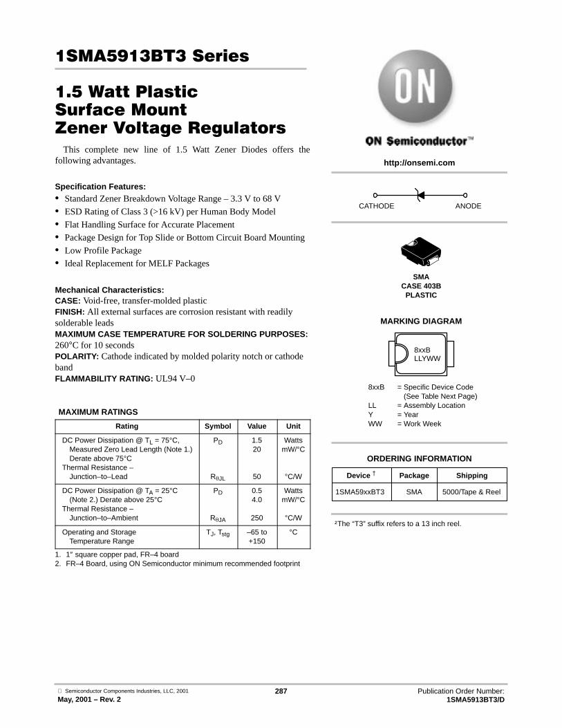
Semiconductor Components Industries, LLC, 2001
May, 2001 – Rev. 2287 Publication Order Number:
1SMA5913BT3/D
1SMA5913BT3 Series
1.5 Watt PlasticSurface MountZener Voltage Regulators
This complete new line of 1.5 Watt Zener Diodes offers thefollowing advantages.
Specification Features:• Standard Zener Breakdown Voltage Range – 3.3 V to 68 V
• ESD Rating of Class 3 (>16 kV) per Human Body Model
• Flat Handling Surface for Accurate Placement
• Package Design for Top Slide or Bottom Circuit Board Mounting
• Low Profile Package
• Ideal Replacement for MELF Packages
Mechanical Characteristics:CASE: Void-free, transfer-molded plasticFINISH: All external surfaces are corrosion resistant with readilysolderable leadsMAXIMUM CASE TEMPERATURE FOR SOLDERING PURPOSES:260°C for 10 secondsPOLARITY: Cathode indicated by molded polarity notch or cathodebandFLAMMABILITY RATING: UL94 V–0
MAXIMUM RATINGS
Rating Symbol Value Unit
DC Power Dissipation @ TL = 75°C,Measured Zero Lead Length (Note 1.)Derate above 75°C
Thermal Resistance –Junction–to–Lead
PD
RJL
1.520
50
WattsmW/°C
°C/W
DC Power Dissipation @ TA = 25°C(Note 2.) Derate above 25°C
Thermal Resistance –Junction–to–Ambient
PD
RJA
0.54.0
250
WattsmW/°C
°C/W
Operating and StorageTemperature Range
TJ, Tstg –65 to+150
°C
1. 1″ square copper pad, FR–4 board2. FR–4 Board, using ON Semiconductor minimum recommended footprint
http://onsemi.com
SMACASE 403B
PLASTIC
8xxB = Specific Device Code= (See Table Next Page)
LL = Assembly LocationY = YearWW = Work Week
8xxBLLYWW
MARKING DIAGRAM
CATHODE ANODE
Device Package Shipping
ORDERING INFORMATION
1SMA59xxBT3 SMA 5000/Tape & Reel
†The “T3” suffix refers to a 13 inch reel.

Zener Voltage Regulator
IF
V
I
IRIZT
VRVZVF
1SMA5913BT3 Series
http://onsemi.com288
ELECTRICAL CHARACTERISTICS (TA = 25°C unlessotherwise noted, VF = 1.5 V Max. @ IF = 200 mA for all types)
Symbol Parameter
VZ Reverse Zener Voltage @ IZT
IZT Reverse Current
ZZT Maximum Zener Impedance @ IZT
IZK Reverse Current
ZZK Maximum Zener Impedance @ IZK
IR Reverse Leakage Current @ VR
VR Reverse Voltage
IF Forward Current
VF Forward Voltage @ IF
IZM Maximum DC Zener Current

1SMA5913BT3 Series
http://onsemi.com289
ELECTRICAL CHARACTERISTICS (TA = 25°C unless otherwise noted, VF = 1.5 V Max. @ IF = 200 mA for all types)
Zener Voltage (Note 4.) Zener Impedance Leakage Current
DeviceVZ (Volts) @ IZT ZZT @ IZT ZZK @ IZK IR @ VR IZM
Device (Note 3.)Device
Marking Min Nom Max mA mA µA Volts mA(dc)
1SMA5913BT3 813B 3.13 3.3 3.47 113.6 10 500 1.0 50 1.0 4551SMA5914BT3 814B 3.42 3.6 3.78 104.2 9.0 500 1.0 35.5 1.0 4171SMA5915BT3 815B 3.70 3.9 4.10 96.1 7.5 500 1.0 12.5 1.0 3851SMA5916BT3 816B 4.08 4.3 4.52 87.2 6.0 500 1.0 2.5 1.0 349
1SMA5917BT3 817B 4.46 4.7 4.94 79.8 5.0 500 1.0 2.5 1.5 3191SMA5918BT3 818B 4.84 5.1 5.36 73.5 4.0 350 1.0 2.5 2.0 2941SMA5919BT3 819B 5.32 5.6 5.88 66.9 2.0 250 1.0 2.5 3.0 2681SMA5920BT3 820B 5.89 6.2 6.51 60.5 2.0 200 1.0 2.5 4.0 242
1SMA5921BT3 821B 6.46 6.8 7.14 55.1 2.5 200 1.0 2.5 5.2 2211SMA5922BT3 822B 7.12 7.5 7.88 50 3.0 400 0.5 2.5 6.0 2001SMA5923BT3 823B 7.79 8.2 8.61 45.7 3.5 400 0.5 2.5 6.5 1831SMA5924BT3 824B 8.64 9.1 9.56 41.2 4.0 500 0.5 2.5 7.0 165
1SMA5925BT3 825B 9.5 10 10.5 37.5 4.5 500 0.25 2.5 8.0 1501SMA5926BT3 826B 10.45 11 11.55 34.1 5.5 550 0.25 0.5 8.4 1361SMA5927BT3 827B 11.4 12 12.6 31.2 6.5 550 0.25 0.5 9.1 1251SMA5928BT3 828B 12.35 13 13.65 28.8 7.0 550 0.25 0.5 9.9 115
1SMA5929BT3 829B 14.25 15 15.75 25 9.0 600 0.25 0.5 11.4 1001SMA5930BT3 830B 15.2 16 16.8 23.4 10 600 0.25 0.5 12.2 941SMA5931BT3 831B 17.1 18 18.9 20.8 12 650 0.25 0.5 13.7 831SMA5932BT3 832B 19 20 21 18.7 14 650 0.25 0.5 15.2 75
1SMA5933BT3 833B 20.9 22 23.1 17 17.5 650 0.25 0.5 16.7 681SMA5934BT3 834B 22.8 24 25.2 15.6 19 700 0.25 0.5 18.2 631SMA5935BT3 835B 25.65 27 28.35 13.9 23 700 0.25 0.5 20.6 561SMA5936BT3 836B 28.5 30 31.5 12.5 26 750 0.25 0.5 22.8 50
1SMA5937BT3 837B 31.35 33 34.65 11.4 33 800 0.25 0.5 25.1 451SMA5938BT3 838B 34.2 36 37.8 10.4 38 850 0.25 0.5 27.4 421SMA5939BT3 839B 37.05 39 40.95 9.6 45 900 0.25 0.5 29.7 381SMA5940BT3 840B 40.85 43 45.15 8.7 53 950 0.25 0.5 32.7 35
1SMA5941BT3 841B 44.65 47 49.35 8.0 67 1000 0.25 0.5 35.8 321SMA5942BT3 842B 48.45 51 53.55 7.3 70 1100 0.25 0.5 38.8 291SMA5943BT3 843B 53.2 56 58.8 6.7 86 1300 0.25 0.5 42.6 271SMA5944BT3 844B 58.9 62 65.1 6.0 100 1500 0.25 0.5 47.1 241SMA5945BT3 845B 64.6 68 71.4 5.5 120 1700 0.25 0.5 51.7 22
3. Tolerance and Voltage Regulation Designation – The type number listed indicates a tolerance of ±5%.4. VZ limits are to be guaranteed at thermal equilibrium.

1SMA5913BT3 Series
http://onsemi.com290
Rating and Typical Characteristic Curves (T A = 25°C)V
Z, T
EM
PE
RAT
UR
E C
OE
FF
ICIE
NT
(mV
/C
)°
θ
0
4
Figure 7. Steady State Power Derating Figure 8. V Z – 3.3 thru 10 Volts
T, TEMPERATURE (°C)
Figure 9. V Z = 12 thru 68 Volts
25 50 75 100 125 150
PD
, MA
XIM
UM
PO
WE
R D
ISS
IPA
TIO
N (
WA
TT
S)
I Z, Z
EN
ER
CU
RR
EN
T (m
A)
Z Z, D
YN
AM
IC IM
PE
DA
NC
E (
OH
MS
)
3.2
2.4
1.6
0.8
00
100
2 4 6 8 10
10
1
0.1
VZ, ZENER VOLTAGE (VOLTS)
100
10
1
0.10 10 20 30 40
VZ, ZENER VOLTAGE (VOLTS)
100
1010 100
VZ, ZENER VOLTAGE (VOLTS)
TL
TA
VZ @ IZT
10 100
VZ, ZENER VOLTAGE (VOLTS)
IZ(dc) = 1 mA
100
10 10 mA
20 mAIZ(rms) = 0.1 IZ(dc)
50
Figure 10. Zener Voltage – 3.3 to 12 Volts
VZ
, TE
MP
ER
ATU
RE
CO
EF
FIC
IEN
T (m
V/
C)
°θ
10
8
6
4
2
0
-2
-42 4 6 8 10
VZ, ZENER VOLTAGE (VOLTS)
VZ @ IZT
12
Figure 11. Zener Voltage – 14 to 68 Volts Figure 12. Effect of Zener Voltage
I Z, Z
EN
ER
CU
RR
EN
T (
mA
)
60 70 80

1SMA5913BT3 Series
http://onsemi.com291
Rating and Typical Characteristic Curves (T A = 25°C)
TA = 25°C
PW (ID) IS DEFINED AS THE
POINT WHERE THE PEAK CURRENT
DECAYS TO 50% OF Ipp.
≤ 10 µs
PEAK VALUE
Ippm
HALF VALUE - Ipp/2
10/1000 µs WAVEFORM
AS DEFINED BY R.E.A.
td
1000
Figure 13. Capacitance Curve Figure 14. Typical Pulse Rating Curve
BREAKDOWN VOLTAGE (VOLTS)
Figure 15. Pulse Waveform Figure 16. Pulse Waveform
10 100
100
100.01
10
0.1 1 10
1
0.1
0.01
TP, PULSE WIDTH (ms)
120
100
80
60
40
00 1 2 3 4
t, TIME (ms)
120
00.1
t, TIME (ms)
MEASURED @
ZERO BIAS
MEASURED @
VZ/2
TJ = 25°C
C, C
APA
CIT
AN
CE
(pF
)
P pk
I ppm
, PE
AK
PU
LSE
CU
RR
EN
T (%
)
NONREPETITIVE, EXPONENTIAL
PULSE WAVEFORM, TJ = 25°C
20
5
100
80
60
40
20
0.04 0.06 0.08
8/20 µs WAVEFORM
AS DEFINED BY ANSI C62.1
AND IEC 801-5.
0.5 IPEAK
0.9 IPEAK
0.1 IPEAK
T
T = 8 µs
20 µs
0 0.02
I ppm
, PE
AK
PU
LSE
CU
RR
EN
T (%
), P
EA
K P
OW
ER
(kW
)

Semiconductor Components Industries, LLC, 2001
May, 2001 – Rev. 1292 Publication Order Number:
1SMB5913BT3/D
1SMB5913BT3 Series
3 Watt Plastic Surface MountZener Voltage Regulators
This complete new line of 3 Watt Zener diodes offers the followingadvantages.
Specification Features:• Zener Voltage Range – 3.3 V to 200 V
• ESD Rating of Class 3 (>16 KV) per Human Body Model
• Flat Handling Surface for Accurate Placement
• Package Design for Top Side or Bottom Circuit Board Mounting
Mechanical Characteristics:CASE: Void-free, transfer-molded plasticFINISH: All external surfaces are corrosion resistant and leads are
readily solderableMAXIMUM LEAD TEMPERATURE FOR SOLDERING PURPOSES:
260°C for 10 SecondsLEADS: Modified L–Bend providing more contact area to bond padsPOLARITY: Cathode indicated by polarity bandFLAMMABILITY RATING: UL94 V–0
MAXIMUM RATINGS
Rating Symbol Value Unit
Maximum Steady State Power Dissipation@ TL = 75°CMeasured at Zero Lead LengthDerate Above 75°C
Thermal Resistance from Junction to Lead
PD
RJL
3.0
4025
W
mW/°C°C/W
Maximum Steady State Power Dissipation@ TA = 25°C (Note 1.)Derate Above 25°C
Thermal Resistance from Junctionto Ambient
PD
RJA
550
4.4226
mW
mW/°C°C/W
Operating and StorageTemperature Range
TJ, Tstg –65 to+150
°C
1. FR–4 board, within 1″ to device, using ON Semiconductor minimumrecommended footprint, as shown in case 403A outline dimensions spec.
PLASTIC SURFACE MOUNTZENER VOLTAGE
REGULATOR DIODES3.3–200 VOLTS
3 WATT DC POWER
Devices listed in bold, italic are ON SemiconductorPreferred devices. Preferred devices are recommendedchoices for future use and best overall value.
Device Package Shipping
ORDERING INFORMATION
1SMB59xxBT3 SMB 2500/Tape & Reel
SMBCASE 403A
PLASTIC
http://onsemi.com
Cathode Anode
Y = YearWW = Work Week9xxB = Specific Device Code
= (See Table Page 294)
YWW9xxB
MARKING DIAGRAM
†The “T3” suffix refers to a 13 inch reel.

Zener Voltage Regulator
IF
V
I
IRIZT
VRVZVF
1SMB5913BT3 Series
http://onsemi.com293
ELECTRICAL CHARACTERISTICS(TL = 30°C unless otherwise noted,VF = 1.5 V Max. @ IF = 200 mA(dc) for all types)
Symbol Parameter
VZ Reverse Zener Voltage @ IZT
IZT Reverse Current
ZZT Maximum Zener Impedance @ IZT
IZK Reverse Current
ZZK Maximum Zener Impedance @ IZK
IR Reverse Leakage Current @ VR
VR Reverse Voltage
IF Forward Current
VF Forward Voltage @ IF
IZM Maximum DC Zener Current

1SMB5913BT3 Series
http://onsemi.com294
ELECTRICAL CHARACTERISTICS (TL = 30°C unless otherwise noted, VF = 1.5 V Max. @ IF = 200 mA(dc) for all types)
Zener Voltage (Note 3.) Zener Impedance (Note 4.) Leakage Current
Device DeviceVZ (Volts) @ IZT ZZT @ IZT ZZK @ IZK IR @ VR IZMDevice
(Note 2.)Device
Marking Min Nom Max mA mA µA Volts mA(dc)
1SMB5913BT3 913B 3.13 3.3 3.47 113.6 10 500 1 100 1 4541SMB5914BT3 914B 3.42 3.6 3.78 104.2 9 500 1 75 1 4161SMB5915BT3 915B 3.70 3.9 4.10 96.1 7.5 500 1 25 1 3841SMB5916BT3 916B 4.08 4.3 4.52 87.2 6 500 1 5 1 348
1SMB5917BT3 917B 4.46 4.7 4.94 79.8 5 500 1 5 1.5 3191SMB5918BT3 918B 4.84 5.1 5.36 73.5 4 350 1 5 2 2941SMB5919BT3 919B 5.32 5.6 5.88 66.9 2 250 1 5 3 2671SMB5920BT3 920B 5.89 6.2 6.51 60.5 2 200 1 5 4 241
1SMB5921BT3 921B 6.46 6.8 7.14 55.1 2.5 200 1 5 5.2 2201SMB5922BT3 922B 7.12 7.5 7.88 50 3 400 0.5 5 6 2001SMB5923BT3 923B 7.79 8.2 8.61 45.7 3.5 400 0.5 5 6.5 1821SMB5924BT3 924B 8.64 9.1 9.56 41.2 4 500 0.5 5 7 164
1SMB5925BT3 925B 9.5 10 10.5 37.5 4.5 500 0.25 5 8 1501SMB5926BT3 926B 10.45 11 11.55 34.1 5.5 550 0.25 1 8.4 1361SMB5927BT3 927B 11.4 12 12.6 31.2 6.5 550 0.25 1 9.1 1251SMB5928BT3 928B 12.35 13 13.65 28.8 7 550 0.25 1 9.9 115
1SMB5929BT3 929B 14.25 15 15.75 25 9 600 0.25 1 11.4 1001SMB5930BT3 930B 15.2 16 16.8 23.4 10 600 0.25 1 12.2 931SMB5931BT3 931B 17.1 18 18.9 20.8 12 650 0.25 1 13.7 831SMB5932BT3 932B 19 20 21 18.7 14 650 0.25 1 15.2 75
1SMB5933BT3 933B 20.9 22 23.1 17 17.5 650 0.25 1 16.7 681SMB5934BT3 934B 22.8 24 25.2 15.6 19 700 0.25 1 18.2 621SMB5935BT3 935B 25.65 27 28.35 13.9 23 700 0.25 1 20.6 551SMB5936BT3 936B 28.5 30 31.5 12.5 28 750 0.25 1 22.8 50
1SMB5937BT3 937B 31.35 33 34.65 11.4 33 800 0.25 1 25.1 451SMB5938BT3 938B 34.2 36 37.8 10.4 38 850 0.25 1 27.4 411SMB5939BT3 939B 37.05 39 40.95 9.6 45 900 0.25 1 29.7 381SMB5940BT3 940B 40.85 43 45.15 8.7 53 950 0.25 1 32.7 34
1SMB5941BT3 941B 44.65 47 49.35 8 67 1000 0.25 1 35.8 311SMB5942BT3 942B 48.45 51 53.55 7.3 70 1100 0.25 1 38.8 291SMB5943BT3 943B 53.2 56 58.8 6.7 86 1300 0.25 1 42.6 261SMB5944BT3 944B 58.9 62 65.1 6 100 1500 0.25 1 47.1 24
1SMB5945BT3 945B 64.6 68 71.4 5.5 120 1700 0.25 1 51.7 221SMB5946BT3 946B 71.25 75 78.75 5 140 2000 0.25 1 56 201SMB5947BT3 947B 77.9 82 86.1 4.6 160 2500 0.25 1 62.2 181SMB5948BT3 948B 86.45 91 95.55 4.1 200 3000 0.25 1 69.2 16
1SMB5949BT3 949B 95 100 105 3.7 250 3100 0.25 1 76 151SMB5950BT3 950B 104.5 110 115.5 3.4 300 4000 0.25 1 83.6 131SMB5951BT3 951B 114 120 126 3.1 380 4500 0.25 1 91.2 121SMB5952BT3 952B 123.5 130 136.5 2.9 450 5000 0.25 1 98.8 11
1SMB5953BT3 953B 142.5 150 157.5 2.5 600 6000 0.25 1 114 101SMB5954BT3 954B 152 160 168 2.3 700 6500 0.25 1 121.6 91SMB5955BT3 955B 171 180 189 2.1 900 7000 0.25 1 136.8 81SMB5956BT3 956B 190 200 210 1.9 1200 8000 0.25 1 152 7
2. TOLERANCE AND TYPE NUMBER DESIGNATIONThe type numbers listed indicate a tolerance of ±5%.
3. ZENER VOLTAGE (VZ) MEASUREMENTNominal Zener voltage is measured with the device junction in thermal equilibrium with ambient temperature at 25°C.
4. ZENER IMPEDANCE (ZZ) DERIVATION ZZT and ZZK are measured by dividing the ac voltage drop across the device by the ac currentapplied. The specified limits are for IZ(ac) = 0.1 IZ(dc) with the ac frequency = 60 Hz.

1SMB5913BT3 Series
http://onsemi.com295
Figure 1. Steady State Power Derating
0 25 50 75 100 125 150
6
5
4
3
2
0
T, TEMPERATURE (°C)
P
, MA
XIM
UM
PO
WE
R D
ISS
IPA
TIO
N (
WA
TT
S)
D
10
20
30
50
100
200
300
500
1K
0.1 0.2 0.3 0.5 1 2 3 5 10 20 30 50 100PW, PULSE WIDTH (ms)
P
, P
EA
K S
UR
GE
PO
WE
R (
WA
TT
S)
PK
Figure 2. Maximum Surge Power
RECTANGULAR
NONREPETITIVE
WAVEFORMTJ=25°C PRIOR
TO INITIAL PULSE
Figure 3. Zener Voltage — To 12 Volts
2 4 6 8 10 12
10
8
6
4
2
0
-2
-4
VZ, ZENER VOLTAGE (VOLTS)
, TE
MP
ER
ATU
RE
CO
EF
FIC
IEN
T (m
V/
C)
°θ V
Z
0 1 2 3 4 5 6 7 8 9 10
100
50
3020
10
1
0.5
0.30.2
0.1
VZ, ZENER VOLTAGE (VOLTS)
2
5
3
0 10 20 30 40 50 60 70 80 90 100
VZ, ZENER VOLTAGE (VOLTS)
100
50
3020
10
1
0.5
0.30.2
0.1
2
53
1
VZ @ IZT
TL
TA
Figure 4. Zener Voltage — 14 To 200 Volts
200
100
70
50
30
20
1010 20 30 50 70 100 200
VZ, ZENER VOLTAGE (VOLTS)
VZ @ IZT
, TE
MP
ER
ATU
RE
CO
EF
FIC
IEN
T (m
V/
C)
°θ V
Z
Figure 5. V Z = 3.3 thru 10 Volts Figure 6. V Z = 12 thru 82 Volts
I ZT,
RE
VE
RS
E C
UR
RE
NT
(m
A)
I ZT,
RE
VE
RS
E C
UR
RE
NT
(m
A)

1SMB5913BT3 Series
http://onsemi.com296
Figure 7. Effect of Zener Voltage
VZ, ZENER VOLTAGE (VOLTS)
5 7 10 20 30 50 70 100
200
100
70
50
30
20
10
7
5
3
2
Z
, DY
NA
MIC
IMP
ED
AN
CE
(O
HM
S)
Z
10mA
IZ(dc) = 1mA
20mA iZ(rms) = 0.1 IZ(dc)
Figure 8. Effect of Zener Current
IZ, ZENER TEST CURRENT (mA)
1k
500
200
100
50
20
10
5
2
10.5 1 2 5 10 20 50 100 200 500
Z
, DY
NA
MIC
IMP
ED
AN
CE
(O
HM
S)
Z
TJ = 25°CiZ(rms) = 0.1 IZ(dc)
VZ =150V
91V
62V
22V
12V6.8V
Rating and Typical Characteristic Curves (T A = 25°C)
TA = 25°C
PW (ID) IS DEFINED AS THE
POINT WHERE THE PEAK CURRENT
DECAYS TO 50% OF Ipp.
≤ 10 µs
PEAK VALUE
Ippm
HALF VALUE - Ipp/2
10/1000 µs WAVEFORM
AS DEFINED BY R.E.A.
td
1000
Figure 9. Capacitance Curve Figure 10. Typical Pulse Rating Curve
BREAKDOWN VOLTAGE (VOLTS)
Figure 11. Pulse Waveform Figure 12. Pulse Waveform
10 100
100
100.01
10
0.1 1 10
1
0.1
0.01
TP, PULSE WIDTH (ms)
120
100
80
60
40
00 1 2 3 4
t, TIME (ms)
120
00.1
t, TIME (ms)
MEASURED @
ZERO BIAS
MEASURED @
VZ/2
TJ = 25°C
C, C
APA
CIT
AN
CE
(pF
)
P pk
I ppm
, PE
AK
PU
LSE
CU
RR
EN
T (%
)
NONREPETITIVE, EXPONENTIAL
PULSE WAVEFORM, TJ = 25°C
20
5
100
80
60
40
20
0.04 0.06 0.08
8/20 µs WAVEFORM
AS DEFINED BY ANSI C62.1
AND IEC 801-5.
0.5 IPEAK
0.9 IPEAK
0.1 IPEAK
T
T = 8 µs
20 µs
0 0.02
I ppm
, PE
AK
PU
LSE
CU
RR
EN
T (%
), P
EA
K P
OW
ER
(kW
)

http://onsemi.com297
CHAPTER 8Surface Mount Information
and Packaging Specifications

http://onsemi.com298

http://onsemi.com299
INFORMATION FOR USING SURFACE MOUNT PACKAGES
RECOMMENDED FOOTPRINTS FOR SURFACE MOUNTED APPLICATIONS
Surface mount board layout is a critical portion of the totaldesign. The footprint for the semiconductor packages mustbe the correct size to ensure proper solder connection
interface between the board and the package. With thecorrect pad geometry, the packages will self align whensubjected to a solder reflow process.
POWER DISSIPATION FOR A SURFACE MOUNT DEVICE
The power dissipation for a surface mount device is afunction of the drain/collector pad size. These can vary fromthe minimum pad size for soldering to a pad size given formaximum power dissipation. Power dissipation for asurface mount device is determined by TJ(max), themaximum rated junction temperature of the die, RθJA, thethermal resistance from the device junction to ambient, andthe operating temperature, TA. Using the values provided onthe data sheet, PD can be calculated as follows:
PD =TJ(max) – TA
RθJA
The values for the equation are found in the maximumratings table on the data sheet. Substituting these values intothe equation for an ambient temperature TA of 25°C, one cancalculate the power dissipation of the device. For example,for a SOT–223 device, PD is calculated as follows.
PD = 150°C – 25°C156°C/W
= 800 milliwatts
The 156°C/W for the SOT–223 package assumes the useof the recommended footprint on a glass epoxy printedcircuit board to achieve a power dissipation of 800milliwatts. There are other alternatives to achieving higherpower dissipation from the surface mount packages. One isto increase the area of the drain/collector pad. By increasingthe area of the drain/collector pad, the power dissipation canbe increased. Although the power dissipation can almost bedoubled with this method, area is taken up on the printedcircuit board which can defeat the purpose of using surfacemount technology. For example, a graph of RθJA versusdrain pad area is shown in Figures 1, 2 and 3.
Another alternative would be to use a ceramic substrate oran aluminum core board such as Thermal Clad . Using aboard material such as Thermal Clad, an aluminum coreboard, the power dissipation can be doubled using the samefootprint.
TO
AM
BIE
NT
(C
/W)
°R
JA, T
HE
RM
AL
RE
SIS
TAN
CE
, JU
NC
TIO
Nθ
0.8 Watts
1.25 Watts* 1.5 Watts
A, AREA (SQUARE INCHES)
0.0 0.2 0.4 0.6 0.8 1.0
160
140
120
100
80
Figure 1. Thermal Resistance versus Drain PadArea for the SOT–223 Package (Typical)
Board Material = 0.0625″G-10/FR-4, 2 oz Copper
TA = 25°C
*Mounted on the DPAK footprint
Figure 2. Thermal Resistance versus Drain PadArea for the DPAK Package (Typical)
1.75 Watts
Board Material = 0.0625″G-10/FR-4, 2 oz Copper
80
100
60
40
201086420
3.0 Watts
5.0 Watts
TA = 25°C
A, AREA (SQUARE INCHES)
TO
AM
BIE
NT
(C
/W)
°R
JA, T
HE
RM
AL
RE
SIS
TAN
CE
, JU
NC
TIO
Nθ
Figure 3. Thermal Resistance versus Drain PadArea for the D 2PAK Package (Typical)
2.5 Watts
A, AREA (SQUARE INCHES)
Board Material = 0.0625″G-10/FR-4, 2 oz Copper TA = 25°C
60
70
50
40
30
201614121086420
3.5 Watts
5 Watts
TO
AM
BIE
NT
(C
/W)
°R
JA, T
HE
RM
AL
RE
SIS
TAN
CE
, JU
NC
TIO
Nθ

http://onsemi.com300
SOLDER STENCIL GUIDELINES
Prior to placing surface mount components onto a printedcircuit board, solder paste must be applied to the pads.Solder stencils are used to screen the optimum amount.These stencils are typically 0.008 inches thick and may bemade of brass or stainless steel. For packages such as theSC–59, SC–70/SOT–323, SOD–123, SOT–23, SOT–143,SOT–223, SO–8, SO–14, SO–16, and SMB/SMC diodepackages, the stencil opening should be the same as the padsize or a 1:1 registration. This is not the case with the DPAKand D2PAK packages. If a 1:1 opening is used to screensolder onto the drain pad, misalignment and/or“tombstoning” may occur due to an excess of solder. Forthese two packages, the opening in the stencil for the pasteshould be approximately 50% of the tab area. The openingfor the leads is still a 1:1 registration. Figure 4 shows atypical stencil for the DPAK and D2PAK packages. The
pattern of the opening in the stencil for the drain pad is notcritical as long as it allows approximately 50% of the pad tobe covered with paste.
ÇÇÇÇÇÇÇÇ
ÇÇÇÇÇÇÇÇÇÇÇÇÇÇÇÇÇÇ
ÇÇÇÇÇÇ
ÇÇÇÇ
Figure 4. Typical Stencil for DPAK andD2PAK Packages
SOLDER PASTE
OPENINGS
STENCIL
SOLDERING PRECAUTIONS
The melting temperature of solder is higher than the ratedtemperature of the device. When the entire device is heatedto a high temperature, failure to complete soldering withina short time could result in device failure. Therefore, thefollowing items should always be observed in order tominimize the thermal stress to which the devices aresubjected.
• Always preheat the device.• The delta temperature between the preheat and
soldering should be 100°C or less.*• When preheating and soldering, the temperature of the
leads and the case must not exceed the maximumtemperature ratings as shown on the data sheet. Whenusing infrared heating with the reflow solderingmethod, the difference should be a maximum of 10°C.
• The soldering temperature and time should not exceed260°C for more than 10 seconds.
• When shifting from preheating to soldering, themaximum temperature gradient shall be 5°C or less.
• After soldering has been completed, the device shouldbe allowed to cool naturally for at least three minutes.Gradual cooling should be used since the use of forcedcooling will increase the temperature gradient and willresult in latent failure due to mechanical stress.
• Mechanical stress or shock should not be applied duringcooling.
* Soldering a device without preheating can causeexcessive thermal shock and stress which can result indamage to the device.
* Due to shadowing and the inability to set the wave heightto incorporate other surface mount components, the D2PAKis not recommended for wave soldering.

http://onsemi.com301
TYPICAL SOLDER HEATING PROFILE
For any given circuit board, there will be a group ofcontrol settings that will give the desired heat pattern. Theoperator must set temperatures for several heating zones anda figure for belt speed. Taken together, these control settingsmake up a heating “profile” for that particular circuit board.On machines controlled by a computer, the computerremembers these profiles from one operating session to thenext. Figure 5 shows a typical heating profile for use whensoldering a surface mount device to a printed circuit board.This profile will vary among soldering systems, but it is agood starting point. Factors that can affect the profileinclude the type of soldering system in use, density and typesof components on the board, type of solder used, and the typeof board or substrate material being used. This profile showstemperature versus time. The line on the graph shows the
actual temperature that might be experienced on the surfaceof a test board at or near a central solder joint. The twoprofiles are based on a high density and a low density board.The Vitronics SMD310 convection/infrared reflowsoldering system was used to generate this profile. The typeof solder used was 62/36/2 Tin Lead Silver with a meltingpoint between 177–189°C. When this type of furnace is usedfor solder reflow work, the circuit boards and solder jointstend to heat first. The components on the board are thenheated by conduction. The circuit board, because it has alarge surface area, absorbs the thermal energy moreefficiently, then distributes this energy to the components.Because of this effect, the main body of a component maybe up to 30 degrees cooler than the adjacent solderjoints.
STEP 1PREHEATZONE 1RAMP"
STEP 2VENTSOAK"
STEP 3HEATINGZONES 2 & 5RAMP"
STEP 4HEATINGZONES 3 & 6SOAK"
STEP 5HEATINGZONES 4 & 7SPIKE"
STEP 6VENT
STEP 7COOLING
200°C
150°C
100°C
50°C
TIME (3 TO 7 MINUTES TOTAL) TMAX
SOLDER IS LIQUID FOR40 TO 80 SECONDS(DEPENDING ONMASS OF ASSEMBLY)
205° TO 219°CPEAK ATSOLDER JOINT
DESIRED CURVE FOR LOWMASS ASSEMBLIES
100°C
150°C
160°C
170°C
140°C
Figure 5. Typical Solder Heating Profile
DESIRED CURVE FOR HIGHMASS ASSEMBLIES

http://onsemi.com302
Footprints for Soldering
SMAmm
inches
0.157
4.0
0.0787
2.0
0.0787
2.0
SMC
0.1714.343
0.1102.794
0.1503.810
mm
inches
SOD–123
ÉÉÉÉÉÉÉÉÉÉÉÉÉÉÉ
ÉÉÉÉÉÉÉÉÉÉÉÉÉÉÉ
0.91
0.036
1.22
0.048
2.36
0.093
4.19
0.165 mm
inches
SMBmm
inches
0.0852.159
0.1082.743
0.0892.261
SOT–23
mm
inches
0.037
0.95
0.037
0.95
0.079
2.0
0.035
0.9
0.031
0.8
SOD–323
0.63mm0.025
1.60mm0.063
2.85mm0.112
0.83mm0.033
mminches

http://onsemi.com303
Footprints for Soldering
SC–74
0.028
0.7
0.074
1.9
0.037
0.95
0.037
0.95
0.094
2.4
0.039
1.0inches
mm
SC–88
ÉÉÉÉÉÉ
ÉÉÉÉÉÉÉÉÉ
ÉÉÉÉÉÉÉÉÉ
ÉÉÉÉÉÉ
ÉÉÉÉÉÉÉÉÉ
ÉÉÉÉÉÉÉÉÉ
0.5 mm (min)
0.4
mm
(m
in)
0.65
mm
0.65
mm
1.9 mm
POWERMITE
0.100
2.54
0.025
0.635
0.050
1.27
0.105
2.670.030
0.762
inches
mm
SC–88A
ÉÉÉÉÉÉ
ÉÉÉÉÉÉÉÉÉ
ÉÉÉÉÉÉÉÉÉ
ÉÉÉÉÉÉ
ÉÉÉÉÉÉÉÉÉ
0.5 mm (min)
0.4
mm
(m
in)
0.65
mm
0.65
mm
1.9 mm

http://onsemi.com304
TVS/Zener Axial-LeadLead Tape Packaging Standards for Axial-LeadComponents
1.0 SCOPE
This section covers packaging requirements for thefollowing axial-lead component’s use in automatic testingand assembly equipment: ON Semiconductor Case 17-02,Case 41A-02, Case 51-02 (DO-7), Case 59-03 (DO-41),Case 59-04, Case 194-04 and Case 299-02 (DO-35).Packaging, as covered in this section, shall consist ofaxial-lead components mounted by their leads on pressuresensitive tape, wound onto a reel.
2.0 PURPOSE
This section establishes ON Semiconductor standardpractices for lead-tape packaging of axial-lead componentsand meets the requirements of EIA Standard RS-296-D“Lead-taping of Components on Axial Lead Configurationfor Automatic Insertion,” level 1.
3.0 REQUIREMENTS
3.1 Component leads
3.1.1 – Component leads shall not be bent beyonddimension E from their normal position. See Figure 2.
3.1.2 – The “C” dimension shall be governed by theoverall length of the reel packaged component. Thedistance between flanges shall be 0.059 inch to 0.315inch greater than the overall component length. SeeFigures 2 and 3.
3.1.3 – Cumulative dimension “A” tolerance shallnot exceed 0.059 over 6 in consecutive components.
3.2 Orientation
All polarized components must be oriented in onedirection. The cathode lead tape shall be blue and theanode tape shall be white. See Figure 1.
3.3 Reeling
3.3.1 – Components on any reel shall not representmore than two date codes when date codeidentification is required.
3.3.2 – Component’s leads shall be positionedperpendicularly between pairs of 0.250 inch tape. SeeFigure 2.
3.3.3 – A minimum 12 inch leader of tape shall beprovided before the first and last component on thereel.
3.3.4 – 50 lb. Kraft paper is wound between layersof components as far as necessary for componentprotection.
3.3.5 – Components shall be centered between tapessuch that the difference between D1 and D2 does notexceed 0.055.
3.3.6 – Staples shall not be used for splicing. No morethan four layers of tape shall be used in any splice areaand no tape shall be offset from another by more than0.031 inch noncumulative. Tape splices shall overlapat least 6 inches for butt joints and at least 3 inches forlap joints and shall not be weaker than unspliced tape.
3.3.7 – Quantity per reel shall be as indicated inTable 1. Orders for tape and reeled product will onlybe processed and shipped in full reel increments.Scheduled orders must be in releases of full reelincrements or multiples thereof.
3.3.8 – A maximum of 0.25% of the componentsper reel quantity may be missing without consecutivemissing per level 1 of RS-296-D.
3.3.9 – The single face roll pad shall be placedaround the finished reel and taped securely. Each reelshall then be placed in an appropriate container.
3.4 Marking
Minimum reel and carton marking shall consist ofthe following (see Figure 3):
ON Semiconductor part number
Quantity
Manufacturer’s name
Date codes (when applicable; see note 3.3.1)
4.0
Requirements differing from this ON Semiconductorstandard shall be negotiated with the factory.
The packages indicated in the following table are suitablefor lead tape packaging. The table indicates the specificdevices (transient voltage suppressors and/or zeners) thatcan be obtained from ON Semiconductor in reel packagingand provides the appropriate packaging specification.

http://onsemi.com305
Lead Tape Packaging Standards for Axial-Lead Components (continued)
Table 1. Packaging Details (all dimensions in inches)
Case TypeProductCategory
DeviceTitle
Suffix
MPQQuantityPer Reel
(Item 3.3.7)
ComponentSpacing
A Dimension
TapeSpacing
B Dimension
ReelDimension
C
ReelDimension
D (Max)
Max OffAlignment
E
Case 17 Surmetic 40 & RL 4000 0.2 +/– 0.015 2.062 +/– 0.059 3 14 0.047600 Watt TVS
Case 41A 1500 Watt TVS RL4 1500 0.4 +/– 0.02 2.062 +/– 0.059 3 14 0.047
Case 51-02 DO-7 Glass RL 3000 0.2 +/– 0.02 2.062 +/– 0.059 3 14 0.047(For Reference only)
Case 59-03 DO-41 Glass & RL 6000 0.2 +/– 0.015 2.062 +/– 0.059 3 14 0.047DO-41 Surmetic 30
Rectifier
Case 59-04 500 Watt TVS RL 5000 0.2 +/– 0.02 2.062 +/– 0.059 3 14 0.047
Rectifier
Case 194-04 110 Amp TVS RL 800 0.4 +/– 0.02 1.875 +/– 0.059 3 14 0.047(Automotive)
Rectifier
Case 267-02 Rectifier RL 1500 0.4 +/– 0.02 2.062 +/– 0.059 3 14 0.047
Case 299 DO-35 Glass RL 5000 0.2 +/– 0.02 2.062 +/– 0.059 3 14 0.047
Kraft Paper
Tape, BlueItem 3.2(Cathode)
Reel
Roll Pad
Container
Tape, WhiteItem 3.2(Anode)
Item 3.1.1Max OffAlignmentE
Item 3.3.5Both Sides
0.250Item 3.3.2
0.031Item 3.3.5
D1 D2
A
OverallLGItem3.1.2
Figure 1. Reel Packing Figure 2. Component Spacing
Optional Design
1.188
Item 3.4
3.5 Dia.
CD
Figure 3. Reel Dimensions
B

http://onsemi.com306
TVS/Zener Surface MountEmbossed Tape and Reel
Embossed Tape and Reel is used to facilitate automatic pick andplace equipment feed requirements. The tape is used as the shippingcontainer for various products and requires a minimum of handling.The antistatic/conductive tape provides a secure cavity for the productwhen sealed with the “peel-back” cover tape.• Used for Automatic Pick and Place Feed Systems
• Minimizes Product Handling
• EIA 481-1, 8 mm and 12 mm Taping of Surface Mount Componentsfor Automatic Handling and EIA 481-2, 16 mm and 24 mmEmbossed Carrier Taping of Surface Mount Components forAutomatic Handling
• SOD-123, SOT-23 in 8 mm Tape, SOD–323
• SMB in 12 mm Tape
• SMC in 16 mm Tape
Ordering InformationUse the standard device title and add the required suffix as listed in
the option table below. Note that the individual reels have a finitenumber of devices depending on the type of product contained in thetape. Also note the minimum lot size is one full reel for each line itemand orders are required to be in increments of the single reel quantity.
SOT-238 mm
SMC16 mm
SOD-123, SOD–3238 mm
SMA, SMB,POWERMITE
12 mm
Tape WidthPitch (1)
Reel SizeDevices Per Reel
and Minim m DevicePackage Case Type
Tape Width(mm) (mm) (in)
Reel Size(inch)*
and MinimumOrder Quantity
DeviceSuffix
SOD-123, SOT-23, Case 318 8 4.0 ± 0.1 .157 ± .004 7 3,000 T1SOD–323 8 13 10,000 T3
SMA Case 403B 12 8.0 ± 0.1 .315 ± .004 13 5,000 T3
SMB Case 403A 12 8.0 ± 0.1 .315 ± .004 13 2,500 T3
SMC Case 403 16 8.0 ± 0.1 .315 ± .004 13 2,500 T3
POWERMITE Case 457 12 8.0 ± 0.1 .315 ± .004 13 12,000 T3
SC–88 Case 419B 8 4.0 ± 0.1 .157 ± .004 7 3,000 T1/T2
SC–88A Case 419A 8 4.0 ± 0.1 .157 ± .004 7 3,000 T1/T2
SC–74 Case 318F 8 4.0 ± 0.1 .157 ± .004 7 3,000 T18 13 10,000 T3
(1)See Next Page.* 7 inch reel = 180 mm, 13 inch reel = 330 mm
Tape and Reel Data for
TVS/Zener Surface Mount
Devices
PACKAGES
SOD-123 SOT-23
SMB SMC

http://onsemi.com307
P0K
t
B1 K0
TOPCOVERTAPE
EMBOSSMENT
USER DIRECTION OF FEED
CENTER LINESOF CAVITY
D P2
10 PITCHESCUMULATIVETOLERANCE ONTAPE± 0.2 mm(± 0.008″)
E
F W
P
B0
A0
D1FOR COMPONENTS2.0 mm x 1.2 mmAND LARGER
* TOP COVERTAPE THICKNESS (t1)0.10 mm(.004″) MAX.
EMBOSSMENT
EMBOSSEDCARRIER
R MIN
BENDING RADIUS
MAXIMUM COMPONENT ROTATION
TYPICALCOMPONENT CAVITYCENTER LINE
TYPICALCOMPONENTCENTER LINE
100 mm(3.937″)
250 mm(9.843″)
1 mm(.039″) MAX
1 mm MAX
10°
TAPE AND COMPONENTSSHALL PASS AROUND RADIUS R"WITHOUT DAMAGE
TAPE
FOR MACHINE REFERENCEONLYINCLUDING DRAFT AND RADIICONCENTRIC AROUND B0
CAMBER (TOP VIEW)ALLOWABLE CAMBER TO BE 1 mm/100 mm NONACCUMULATIVE OVER 250 mm
SEENOTE 1
BAR CODELABEL
CARRIER TAPE SPECIFICATIONS
DIMENSIONSTape
Size
B1
Max(2) D D1 E F K P P0 P2 R Min T Max W Max
8mm 4.55mm(.179″)
1.5+0.1mm-0.0
( 0 9 00 ″
1.0Min(.039″)
1.75± 0.1mm(.069± .004″)
3.5± 0.05mm(.138± .002″)
2.4mmMax(.094″)
4.0± 0.1mm(.157± .004″)
4.0± 0.1mm(.157± .004″)
2.0± 0.1mm(.079± .002″)
25mm(.98″)
0.6mm(.024″)
8.3mm(.327″)
12mm 8.2mm(.323″)
0.0(.059+.004″
-0.0) 1.5mmMin(.060″)
(.069± .004 )
5.5± 0.05mm(.217± .002″)
6.4mmMax(.252″)
4.0± 0.1mm(.157± .004″)
8.0± 0.1mm(.315± .004″)
(.157± .004 ) (.079± .002 )
30mm(1.18″)
(.024 )
12± .30mm(.470± .012″)
16mm 12.1mm(.476″)
7.5± 0.10mm(.295± .004″)
7.9mmMax(.311″)
4.0± 0.1mm(.157± .004″)
8.0± 0.1mm(.315± .004″)
12.0± 0.1 mm(.472± .004″)
16.3mm(.642″)
24mm 20.1mm(.791″)
11.5± 0.1mm(.453± .004″)
11.9mmMax(.468″)
16.0± .01mm(.63± .004″)
24.3mm(.957″)
Metric dimensions govern – English are in parentheses for reference only.
NOTE 1: A0, B0, and K0 are determined by component size. The clearance between the components and the cavity must be within .05 mm min. to .5 mm max.,NOTE 1: the component cannot rotate more than 10° within the determined cavity.
NOTE 2: If B1 exceeds 4.2 mm (.165) for 8 mm embossed tape, the tape may not feed through all tape feeders.

http://onsemi.com308
REEL CONFIGURATIONMetric Dimensions Govern — English are in parentheses for reference only
A
FULL RADIUS
T MAX
G
20.2 mm MIN(.795″)
1.5 mm MIN(.06″)
13.0 mm ± 0.5 mm(.512″ ± .002″)
50 mm MIN(1.969″)
OUTSIDE DIMENSIONMEASURED AT EDGE
INSIDE DIMENSIONMEASURED NEAR HUB
Size A Max G T Max
8 mm 330 mm(12.992″)
8.4 mm + 1.5 mm, –0.0(.33″ + .059″, –0.00)
14.4 mm(.56″)
12 mm 330 mm(12.992″)
12.4 mm + 2.0 mm, –0.0(.49″ + .079″, –0.00)
18.4 mm(.72″)
16 mm 360 mm(14.173″)
16.4 mm + 2.0 mm, –0.0(.646″ + .078″, –0.00)
22.4 mm(.882″)
24 mm 360 mm(14.173″)
24.4 mm + 2.0 mm, –0.0(.961″ + .070″, –0.00)
30.4 mm(1.197″)

http://onsemi.com309
TAPE LEADER AND TRAILER DIMENSIONS
Metric dimensions govern
NOTES
1. There shall be a leader of 230 mm (9.05) minimum which may consist of carrier and/or cover tape followed by a minimum of 160 mm (6.30) of empty carrier tape sealed with cover tape.
2. There shall be a trailer of 160 mm (6.30) minimum of empty carrier tape sealed with cover tape. The entire carriertape must release from the reel hub as the last portion of the tape unwinds from the reel without damage to thecarrier tape and the remaining components in the cavities.
Trailer(Note 2)160 mm
(6.30) MinTop Cover Tape
END
Carrier Tape
Leader(Note 1)390 mm
(15.35) Min
Cover Tape
START
Components
ELECTRICAL POLARIZATION
Metric dimensions govern
TWO TERMINATION DEVICES
NOTES
1. All polarized components must be oriented in one direction. For components with two terminations the cathodeshall be adjacent to the sprocket hole side.
User Direction of FeedTop Cover Tape Removed

http://onsemi.com310

http://onsemi.com311
CHAPTER 9Package Outline Dimensions

http://onsemi.com312
Package Outline Dimensions
SURMETIC 40CASE 17–02
ISSUE C
B
D
FK
A
FK
DIM MIN MAX MIN MAX
MILLIMETERSINCHES
A 0.330 0.350 8.38 8.89
B 0.130 0.145 3.30 3.68D 0.037 0.043 0.94 1.09F --- 0.050 --- 1.27K 1.000 1.250 25.40 31.75
NOTES:1. LEAD DIAMETER AND FINISH NOT CONTROLLED
WITHIN DIMENSION F.
STYLE 1:PIN 1. ANODE
2. CATHODE
2
1
MOSORBCASE 41A–02
ISSUE A
DIMA
MIN MAX MIN MAX
MILLIMETERS
0.360 0.375 9.14 9.52
INCHES
B 0.190 0.205 4.83 5.21D 0.038 0.042 0.97 1.07K 1.00 --- 25.40 ---P --- 0.050 --- 1.27
NOTES:1. DIMENSIONING AND TOLERANCING PER ANSI
Y14.5M, 1982.2. CONTROLLING DIMENSION: INCH.3. LEAD FINISH AND DIAMETER
UNCONTROLLED IN DIMENSION P.
D
K
P
PA
K
B

http://onsemi.com313
PACKAGE OUTLINE DIMENSIONS (continued)
GLASS/PLASTICDO–41
CASE 59–03ISSUE M
B
DK
KF
F
A
DIM MIN MAX MIN MAX
INCHESMILLIMETERS
A 4.07 5.20 0.160 0.205B 2.04 2.71 0.080 0.107D 0.71 0.86 0.028 0.034
F --- 1.27 --- 0.050K 27.94 --- 1.100 ---
NOTES:1. ALL RULES AND NOTES ASSOCIATED WITH
JEDEC DO-41 OUTLINE SHALL APPLY.2. POLARITY DENOTED BY CATHODE BAND.3. LEAD DIAMETER NOT CONTROLLED WITHIN F
DIMENSION.
MINI MOSORBCASE 59–04
ISSUE M
K
A
DK
B
DIM MIN MAX MIN MAX
INCHESMILLIMETERS
A 5.97 6.60 0.235 0.260B 2.79 3.05 0.110 0.120
D 0.76 0.86 0.030 0.034K 27.94 --- 1.100 ---
NOTES:1. ALL RULES AND NOTES ASSOCIATED WITH
JEDEC DO-41 OUTLINE SHALL APPLY.2. POLARITY DENOTED BY CATHODE BAND.3. LEAD DIAMETER NOT CONTROLLED WITHIN F
DIMENSION.
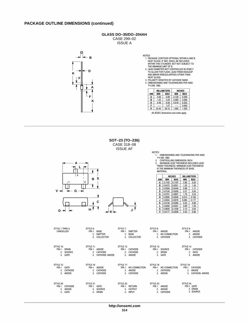
http://onsemi.com314
PACKAGE OUTLINE DIMENSIONS (continued)
GLASS DO–35/DO–204AHCASE 299–02
ISSUE A
NOTES:1. PACKAGE CONTOUR OPTIONAL WITHIN A AND B
HEAT SLUGS, IF ANY, SHALL BE INCLUDEDWITHIN THIS CYLINDER, BUT NOT SUBJECT TOTHE MINIMUM LIMIT OF B.
2. LEAD DIAMETER NOT CONTROLLED IN ZONE FTO ALLOW FOR FLASH, LEAD FINISH BUILDUPAND MINOR IRREGULARITIES OTHER THANHEAT SLUGS.
3. POLARITY DENOTED BY CATHODE BAND.4. DIMENSIONING AND TOLERANCING PER ANSI
Y14.5M, 1982.
All JEDEC dimensions and notes apply.
DIM MIN MAX MIN MAX
INCHESMILLIMETERS
A 3.05 5.08 0.120 0.200B 1.52 2.29 0.060 0.090D 0.46 0.56 0.018 0.022F --- 1.27 --- 0.050K 25.40 38.10 1.000 1.500
B
DK
KF
F
A
SOT–23 (TO–236)CASE 318–08
ISSUE AF
STYLE 22:PIN 1. RETURN
2. OUTPUT3. INPUT
STYLE 6:PIN 1. BASE
2. EMITTER3. COLLECTOR
STYLE 7:PIN 1. EMITTER
2. BASE3. COLLECTOR
STYLE 8:PIN 1. ANODE
2. NO CONNECTION3. CATHODE
STYLE 9:PIN 1. ANODE
2. ANODE3. CATHODE
STYLE 10:PIN 1. DRAIN
2. SOURCE3. GATE
STYLE 11:PIN 1. ANODE
2. CATHODE3. CATHODE-ANODE
STYLE 12:PIN 1. CATHODE
2. CATHODE3. ANODE
STYLE 13:PIN 1. SOURCE
2. DRAIN3. GATE
STYLE 14:PIN 1. CATHODE
2. GATE3. ANODE
STYLE 15:PIN 1. GATE
2. CATHODE3. ANODE
STYLE 16:PIN 1. ANODE
2. CATHODE3. CATHODE
STYLE 17:PIN 1. NO CONNECTION
2. ANODE3. CATHODE
STYLE 18:PIN 1. NO CONNECTION
2. CATHODE3. ANODE
STYLE 19:PIN 1. CATHODE
2. ANODE3. CATHODE-ANODE
STYLE 23:PIN 1. ANODE
2. ANODE3. CATHODE
STYLE 20:PIN 1. CATHODE
2. ANODE3. GATE
STYLE 21:PIN 1. GATE
2. SOURCE3. DRAIN
STYLE 1 THRU 5:CANCELLED
STYLE 24:PIN 1. GATE
2. DRAIN 3. SOURCE
D JK
LA
C
B S
H
GV
3
1 2DIM
A
MIN MAX MIN MAX
MILLIMETERS
0.1102 0.1197 2.80 3.04
INCHES
B 0.0472 0.0551 1.20 1.40C 0.0350 0.0440 0.89 1.11D 0.0150 0.0200 0.37 0.50G 0.0701 0.0807 1.78 2.04H 0.0005 0.0040 0.013 0.100J 0.0034 0.0070 0.085 0.177K 0.0140 0.0285 0.35 0.69L 0.0350 0.0401 0.89 1.02S 0.0830 0.1039 2.10 2.64
V 0.0177 0.0236 0.45 0.60
NOTES:1. DIMENSIONING AND TOLERANCING PER ANSI
Y14.5M, 1982.2. CONTROLLING DIMENSION: INCH.3. MAXIMUM LEAD THICKNESS INCLUDES LEAD
FINISH THICKNESS. MINIMUM LEAD THICKNESSIS THE MINIMUM THICKNESS OF BASEMATERIAL.

http://onsemi.com315
PACKAGE OUTLINE DIMENSIONS (continued)
SC–74CASE 318F–03
ISSUE E
STYLE 1:PIN 1. CATHODE
2. ANODE3. CATHODE4. CATHODE5. ANODE6. CATHODE
2 3
456
A
L
1S
GD
B
H
C0.05 (0.002)
DIM MIN MAX MIN MAX
MILLIMETERSINCHES
A 0.1142 0.1220 2.90 3.10B 0.0512 0.0669 1.30 1.70C 0.0354 0.0433 0.90 1.10D 0.0098 0.0197 0.25 0.50G 0.0335 0.0413 0.85 1.05H 0.0005 0.0040 0.013 0.100J 0.0040 0.0102 0.10 0.26K 0.0079 0.0236 0.20 0.60L 0.0493 0.0649 1.25 1.65M 0 10 0 10
S 0.0985 0.1181 2.50 3.00
NOTES:1. DIMENSIONING AND TOLERANCING PER ANSI
Y14.5M, 1982.2. CONTROLLING DIMENSION: INCH.3. MAXIMUM LEAD THICKNESS INCLUDES LEAD
FINISH THICKNESS. MINIMUM LEAD THICKNESSIS THE MINIMUM THICKNESS OF BASEMATERIAL.
4. 318F-01 AND -02 OBSOLETE. NEW STANDARD318F-03.
MJ
K
STYLE 2:PIN 1. NO CONNECTION
2. COLLECTOR3. EMITTER4. NO CONNECTION5. COLLECTOR6. BASE
SMCCASE 403–03
ISSUE BS
A
D B
JPK H
C
DIM MIN MAX MIN MAX
MILLIMETERSINCHES
A 0.260 0.280 6.60 7.11B 0.220 0.240 5.59 6.10C 0.075 0.095 1.90 2.41D 0.115 0.121 2.92 3.07H 0.0020 0.0060 0.051 0.152J 0.006 0.012 0.15 0.30K 0.030 0.050 0.76 1.27P 0.020 REF 0.51 REFS 0.305 0.320 7.75 8.13
NOTES:1. DIMENSIONING AND TOLERANCING PER ANSI
Y14.5M, 1982.2. CONTROLLING DIMENSION: INCH.3. D DIMENSION SHALL BE MEASURED WITHIN
DIMENSION P.

http://onsemi.com316
PACKAGE OUTLINE DIMENSIONS (continued)
SMBD0–214AA
CASE 403A–03ISSUE D
A
S
D B
JPK
C
H
NOTES:1. DIMENSIONING AND TOLERANCING PER ANSI
Y14.5M, 1982.2. CONTROLLING DIMENSION: INCH.3. D DIMENSION SHALL BE MEASURED WITHIN
DIMENSION P.
DIM MIN MAX MIN MAX
MILLIMETERSINCHES
A 0.160 0.180 4.06 4.57B 0.130 0.150 3.30 3.81C 0.075 0.095 1.90 2.41D 0.077 0.083 1.96 2.11H 0.0020 0.0060 0.051 0.152J 0.006 0.012 0.15 0.30K 0.030 0.050 0.76 1.27P 0.020 REF 0.51 REFS 0.205 0.220 5.21 5.59
SMACASE 403B–01
ISSUE O
NOTES:1. DIMENSIONING AND TOLERANCING PER ANSI
Y14.5M, 1982.2. CONTROLLING DIMENSION: INCH.
S
A
D B
K J
C
H
DIM MIN MAX MIN MAX
MILLIMETERSINCHES
A 0.160 0.180 4.06 4.57B 0.090 0.115 2.29 2.92C 0.075 0.105 1.91 2.67D 0.050 0.064 1.27 1.63H 0.004 0.008 0.10 0.20J 0.006 0.016 0.15 0.41K 0.030 0.060 0.76 1.52S 0.190 0.220 4.83 5.59

http://onsemi.com317
PACKAGE OUTLINE DIMENSIONS (continued)
SOD–123CASE 425–04
ISSUE C
NOTES:1. DIMENSIONING AND TOLERANCING PER ANSI
Y14.5M, 1982.2. CONTROLLING DIMENSION: INCH.
STYLE 1:PIN 1. CATHODE
2. ANODE
ÂÂÂÂÂÂ
B
D
K
A C
E
J
1
2
H
DIM MIN MAX MIN MAX
MILLIMETERSINCHES
A 0.055 0.071 1.40 1.80B 0.100 0.112 2.55 2.85C 0.037 0.053 0.95 1.35D 0.020 0.028 0.50 0.70E 0.01 --- 0.25 ---H 0.000 0.004 0.00 0.10J --- 0.006 --- 0.15K 0.140 0.152 3.55 3.85
SOD–323CASE 477–02
ISSUE B
NOTES:1. DIMENSIONING AND TOLERANCING PER ANSI
Y14.5M, 1982.2. CONTROLLING DIMENSION: MILLIMETERS.3. LEAD THICKNESS SPECIFIED PER L/F DRAWING
WITH SOLDER PLATING.
DIM MIN MAX MIN MAX
INCHESMILLIMETERS
A 1.60 1.80 0.063 0.071B 1.15 1.35 0.045 0.053C 0.80 1.00 0.031 0.039
D 0.25 0.40 0.010 0.016E 0.15 REF 0.006 REFH 0.00 0.10 0.000 0.004J 0.089 0.177 0.0035 0.0070K 2.30 2.70 0.091 0.106
NOTE 3
AK
1 2D B
E
H
C
J
STYLE 1:PIN 1. CATHODE
2. ANODE
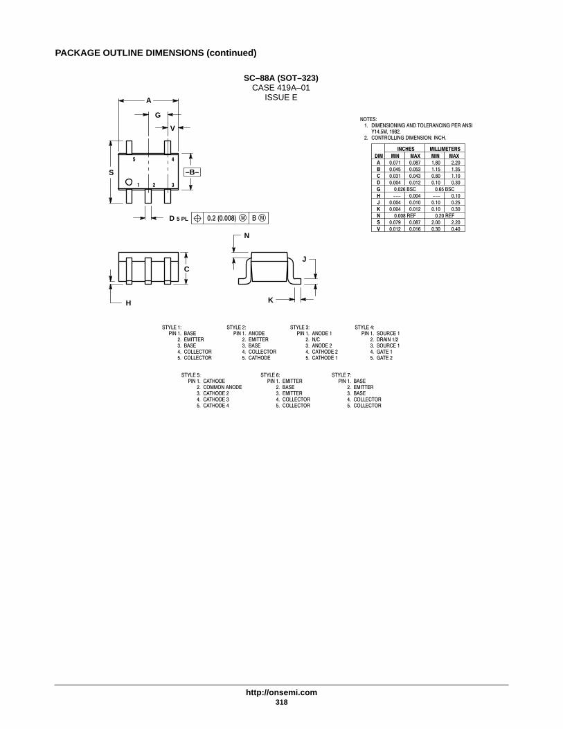
http://onsemi.com318
PACKAGE OUTLINE DIMENSIONS (continued)
SC–88A (SOT–323)CASE 419A–01
ISSUE E
NOTES:1. DIMENSIONING AND TOLERANCING PER ANSI
Y14.5M, 1982.2. CONTROLLING DIMENSION: INCH.
DIM
A
MIN MAX MIN MAX
MILLIMETERS
1.80 2.200.071 0.087
INCHES
B 1.15 1.350.045 0.053
C 0.80 1.100.031 0.043D 0.10 0.300.004 0.012G 0.65 BSC0.026 BSCH --- 0.10---0.004J 0.10 0.250.004 0.010K 0.10 0.300.004 0.012N 0.20 REF0.008 REFS 2.00 2.200.079 0.087V 0.30 0.400.012 0.016
STYLE 1:PIN 1. BASE
2. EMITTER 3. BASE 4. COLLECTOR 5. COLLECTOR
STYLE 2:PIN 1. ANODE
2. EMITTER 3. BASE 4. COLLECTOR 5. CATHODE
B0.2 (0.008) M M
1 2 3
45
A
G
V
S
D 5 PL
H
C
N
J
K
–B–
STYLE 3:PIN 1. ANODE 1
2. N/C 3. ANODE 2 4. CATHODE 2 5. CATHODE 1
STYLE 4:PIN 1. SOURCE 1
2. DRAIN 1/2 3. SOURCE 1 4. GATE 1 5. GATE 2
STYLE 5:PIN 1. CATHODE
2. COMMON ANODE 3. CATHODE 2 4. CATHODE 3 5. CATHODE 4
STYLE 7:PIN 1. BASE
2. EMITTER 3. BASE 4. COLLECTOR 5. COLLECTOR
STYLE 6:PIN 1. EMITTER
2. BASE 3. EMITTER 4. COLLECTOR 5. COLLECTOR

http://onsemi.com319
PACKAGE OUTLINE DIMENSIONS (continued)
SC–88 (SOT–363)CASE 419B–01
ISSUE G
NOTES:1. DIMENSIONING AND TOLERANCING PER ANSI
Y14.5M, 1982.2. CONTROLLING DIMENSION: INCH.
DIM
A
MIN MAX MIN MAX
MILLIMETERS
1.80 2.200.071 0.087
INCHES
B 1.15 1.350.045 0.053C 0.80 1.100.031 0.043D 0.10 0.300.004 0.012G 0.65 BSC0.026 BSCH --- 0.10---0.004J 0.10 0.250.004 0.010K 0.10 0.300.004 0.012N 0.20 REF0.008 REFS 2.00 2.200.079 0.087
V 0.30 0.400.012 0.016
B0.2 (0.008) M M
1 2 3
A
GV
S
H
C
N
J
K
6 5 4
–B–
D 6 PL
STYLE 1:PIN 1. EMITTER 2
2. BASE 2 3. COLLECTOR 1 4. EMITTER 1 5. BASE 1 6. COLLECTOR 2
STYLE 3:CANCELLED
STYLE 2:CANCELLED
STYLE 4:PIN 1. CATHODE
2. CATHODE 3. COLLECTOR 4. EMITTER 5. BASE 6. ANODE
STYLE 5:PIN 1. ANODE
2. ANODE 3. COLLECTOR 4. EMITTER 5. BASE 6. CATHODE
STYLE 6:PIN 1. ANODE 2
2. N/C 3. CATHODE 1 4. ANODE 1 5. N/C 6. CATHODE 2
STYLE 7:PIN 1. SOURCE 2
2. DRAIN 2 3. GATE 1 4. SOURCE 1 5. DRAIN 1 6. GATE 2
STYLE 8:CANCELLED
STYLE 11:PIN 1. CATHODE 2
2. CATHODE 2 3. ANODE 1 4. CATHODE 1 5. CATHODE 1 6. ANODE 2
STYLE 9:PIN 1. EMITTER 2
2. EMITTER 1 3. COLLECTOR 1 4. BASE 1 5. BASE 2 6. COLLECTOR 2
STYLE 10:PIN 1. SOURCE 2
2. SOURCE 1 3. GATE 1 4. DRAIN 1 5. DRAIN 2 6. GATE 2
STYLE 12:PIN 1. ANODE 2
2. ANODE 2 3. CATHODE 1 4. ANODE 1 5. ANODE 1 6. CATHODE 2
STYLE 13:PIN 1. ANODE
2. N/C 3. COLLECTOR 4. EMITTER 5. BASE 6. CATHODE
STYLE 14:PIN 1. VREF
2. GND 3. GND 4. IOUT 5. VEN 6. VCC
STYLE 15:PIN 1. ANODE
2. ANODE 3. ANODE 4. CATHODE 5. CATHODE 6. CATHODE
STYLE 17:PIN 1. BASE 1
2. EMITTER 1 3. COLLECTOR 2 4. BASE 2 5. EMITTER 2 6. COLLECTOR 1
STYLE 16:PIN 1. BASE 1
2. EMITTER 2 3. COLLECTOR 2 4. BASE 2 5. EMITTER 1 6. COLLECTOR 1
STYLE 18:PIN 1. VIN1
2. VCC 3. VOUT2 4. VIN2 5. GND 6. VOUT1
STYLE 19:PIN 1. I OUT
2. GND 3. GND 4. V CC 5. V EN 6. V REF

http://onsemi.com320
PACKAGE OUTLINE DIMENSIONS (continued)
POWERMITECASE 457–04
ISSUE D
DIM MIN MAX MIN MAX
INCHESMILLIMETERS
A 1.75 2.05 0.069 0.081B 1.75 2.18 0.069 0.086C 0.85 1.15 0.033 0.045
D 0.40 0.69 0.016 0.027F 0.70 1.00 0.028 0.039H -0.05 +0.10 -0.002 +0.004J 0.10 0.25 0.004 0.010K 3.60 3.90 0.142 0.154L 0.50 0.80 0.020 0.031R 1.20 1.50 0.047 0.059S
NOTES:1. DIMENSIONING AND TOLERANCING PER ANSI
Y14.5M, 1982.2. CONTROLLING DIMENSION: MILLIMETER.3. DIMENSION A DOES NOT INCLUDE MOLD FLASH,
PROTRUSIONS OR GATE BURRS. MOLD FLASH,PROTRUSIONS OR GATE BURRS SHALL NOTEXCEED 0.15 (0.006) PER SIDE.
SBM0.08 (0.003) C ST
–A–
–B–
S
J
K
–T–
H
L
J
C
D
SBM0.08 (0.003) C ST
F
TERM. 1
TERM. 2
R
0.50 REF 0.019 REF

http://onsemi.com321
CHAPTER 10Technical Information,
Application Notes and Articles
http://onsemi.com322
Technical Information, Application Notes and ArticlesZener Diode Theory 323. . . . . . . . . . . . . . . . . . . . . . . . . . . Zener Diode Fabrication Techniques 328. . . . . . . . . . . . . Reliability 332. . . . . . . . . . . . . . . . . . . . . . . . . . . . . . . . . . . . Zener Diode Characteristics 338. . . . . . . . . . . . . . . . . . . . Temperature Compensated Zeners 350. . . . . . . . . . . . . . Basic Voltage Regulation Using Zener Diodes 354. . . . Zener Protective Circuits and Techniques:
Basic Design Considerations 364. . . . . . . . . . . . . . . . Zener Voltage Sensing Circuits and Applications 374. . Miscellaneous Applications of
Zener Type Devices 381. . . . . . . . . . . . . . . . . . . . . . . . Transient Voltage Suppression 383. . . . . . . . . . . . . . . . . AN784 402. . . . . . . . . . . . . . . . . . . . . . . . . . . . . . . . . . . . . . AN843 404. . . . . . . . . . . . . . . . . . . . . . . . . . . . . . . . . . . . . . Design Considerations and Performance of
Temperature Compensated Zener Diodes 417. . . . . MOSORBs 422. . . . . . . . . . . . . . . . . . . . . . . . . . . . . . . . . . . AR450 426. . . . . . . . . . . . . . . . . . . . . . . . . . . . . . . . . . . . . . Measurement of Zener Voltage to Thermal
Equilibrium with Pulsed Test Current 439. . . . . . . . . . Sales Office List 447. . . . . . . . . . . . . . . . . . . . . . . . . . . . . . Standard Document Type Definitions 448. . . . . . . . . . . .

http://onsemi.com323
ZENER DIODE THEORY
INTRODUCTION
The zener diode is a semiconductor device unique in itsmode of operation and completely unreplaceable by anyother electronic device. Because of its unusual properties itfills a long-standing need in electronic circuitry. It provides,among other useful functions, a constant voltage referenceor voltage control element available over a wide spectrum ofvoltage and power levels.
The zener diode is unique among the semiconductorfamily of devices because its electrical properties arederived from a rectifying junction which operates in thereverse breakdown region. In the sections that follow, thereverse biased rectifying junction, some of the termsassociated with it, and properties derived from it will bediscussed fully.
The zener diode is fabricated from the element silicon.Special techniques are applied in the fabrication of zenerdiodes to create the required properties.
This manual was prepared to acquaint the engineer, theequipment designer and manufacturer, and the experimenterwith the fundamental principles, design characteristics,applications and advantages of this importantsemiconductor device.
SEMICONDUCTOR THEORY
The active portion of a zener diode is a semiconductor PNjunction. PN junctions are formed in various kinds ofsemiconductor devices by several techniques. Among theseare the widely used techniques known as alloying anddiffusion which are utilized in fabricating zener PNjunctions to provide excellent control over zener breakdownvoltage.
At the present time, zener diodes use silicon as the basicmaterial in the formation of their PN junction. Silicon is inGroup IV of the periodic table (tetravalent) and is classed asa “semiconductor” due to the fact that it is a poor conductorin a pure state. When controlled amounts of certain“impurities” are added to a semiconductor it becomes abetter conductor of electricity. Depending on the type ofimpurity added to the basic semiconductor, its conductivitymay take two different forms, called P- and N-typerespectively.
N-type conductivity in a semiconductor is much like theconductivity due to the drift of free electrons in a metal. Inpure silicon at room temperature there are too few freeelectrons to conduct current. However, there are ways ofintroducing free electrons into the crystal lattice as we shall
now see. Silicon is a tetravalent element, one with fourvalence electrons in the outer shell; all are virtually lockedinto place by the covalent bonds of the crystal latticestructure, as shown schematically in Figure 1a. Whencontrolled amounts of donor impurities (Group V elements)such as phosphorus are added, the pentavalent phosphorusatoms entering the lattice structure provide extra electronsnot required by the covalent bonds. These impurities arecalled donor impurities since they “donate” a free electronto the lattice. These donated electrons are free to drift fromnegative to positive across the crystal when a field is applied,as shown in Figure 1b. The “N” nomenclature for this kindof conductivity implies “negative” charge carriers.
In P-type conductivity, the charges that carry electriccurrent across the crystal act as if they were positive charges.We know that electricity is always carried by driftingelectrons in any material, and that there are no mobilepositively charged carriers in a solid. Positive chargecarriers can exist in gases and liquids in the form of positiveions but not in solids. The positive character of the currentflow in the semiconductor crystal may be thought of as themovement of vacancies (called holes) in the covalent lattice.These holes drift from positive toward negative in an electricfield, behaving as if they were positive carriers.
P-type conductivity in semiconductors result from addingacceptor impurities (Group III elements) such as boron tosilicon to the semiconductor crystal. In this case, boronatoms, with three valence electrons, enter the tetravalentsilicon lattice. Since the covalent bonds cannot be satisfiedby only three electrons, each acceptor atom leaves a hole inthe lattice which is deficient by one electron. These holesreadily accept electrons introduced by external sources orcreated by radiation or heat, as shown in Figure 1c. Hencethe name acceptor ion or acceptor impurity. When anexternal circuit is connected, electrons from the currentsource “fill up” these holes from the negative end and jumpfrom hole to hole across the crystal or one may think of thisprocess in a slightly different but equivalent way, that is asthe displacement of positive holes toward the negativeterminal. It is this drift of the positively charged holes whichaccounts for the term P-type conductivity.
When semiconductor regions of N- and P-typeconductivities are formed in a semiconductor crystaladjacent to each other, this structure is called a PN junction.Such a junction is responsible for the action of both zenerdiodes and rectifier devices, and will be discussed in the nextsection.

http://onsemi.com324
Figure 1. Semiconductor Structure
-
Si
Si Si Si
Si
Si Si
Si
Si P Si
Si
Si Si
Si
Si B Si
Si
Si Si
APPLIED FIELD
APPLIED FIELD
+
ELECTRONS ARE LOCKED
IN COVALENT BONDS
LOCKED COVALENT
BOND ELECTRONS
FREE ELECTRON
FROM PHOSPHOROUS
ATOM DRIFTS TOWARD
APPLIED POSITIVE POLE.
INCOMPLETED
COVALENT BOND
THIS ELECTRON JUMPS INTO
HOLE LEFT BY BORON ATOM.
HOLE POSITION IS DISPLACED
TO RIGHT. THIS RESULTS IN
A DRIFT OF HOLES TOWARD
THE NEGATIVE POLE, GIVING
THEM THE CHARACTER OF
MOBILE POSITIVE CHARGES.
(a) Lattice Structures ofPure Silicon
(b) N-Type Silicon
(c) P-Type Silicon
-
THE SEMICONDUCTOR DIODE
In the forward-biased PN junction, Figure 2a, the P regionis made more positive than the N region by an externalcircuit. Under these conditions there is a very low resistanceto current flow in the circuit. This is because the holes in thepositive P-type material are very readily attracted across thejunction interface toward the negative N-type side.
Conversely, electrons in the N-type are readily attracted bythe positive polarity in the other direction.
When a PN junction is reverse biased, the P-type side ismade more negative than the N-type side. (See Figure 2b.)At voltages below the breakdown of the junction, there isvery little current flow across the junction interface. At firstthought one would expect no reverse current under reversebias conditions, but several effects are responsible for thissmall current.
Under this condition the positive holes in the P-typesemiconductor are repelled from the junction interface bythe positive polarity applied to the N side, and conversely,the electrons in the N material are repelled from the interfaceby the negative polarity of the P side. This creates a regionextending from the junction interface into both P- andN-type materials which is completely free of charge carriers,that is, the region is depleted of its charge carriers. Hence,this region is usually called the depletion region.
Although the region is free of charge carriers, the P-sideof the depletion region will have an excess negative chargedue to the presence of acceptor ions which are, of course,fixed in the lattice; while the N-side of the depletion regionhas an excess positive charge due to the presence of donorions. These opposing regions of charged ions create a strongelectric field across the PN junction responsible for thecreation of reverse current.
The semiconductor regions are never perfect; there arealways a few free electrons in P material and few holes in Nmaterial. A more significant factor, however, is the fact thatgreat magnitudes of electron-hole pairs may be thermallygenerated at room temperatures in the semiconductor. Whenthese electron-hole pairs are created within the depletionregion, then the intense electric field mentioned in the aboveparagraph will cause a small current to flow. This smallcurrent is called the reverse saturation current, and tends tomaintain a relatively constant value for a fixed temperatureat all voltages. The reverse saturation current is usuallynegligible compared with the current flow when the junctionis forward biased. Hence, we see that the PN junction, whennot reverse biased beyond breakdown voltage, will conductheavily in only one direction. When this property is utilizedin a circuit we are employing the PN junction as a rectifier.Let us see how we can employ its reverse breakdowncharacteristics to an advantage.
As the reverse voltage is increased to a point called thevoltage breakdown point and beyond, current conductionacross the junction interface increases rapidly. The breakfrom a low value of the reverse saturation current to heavyconductance is very sharp and well defined in most PNjunctions. It is called the zener knee. When reverse voltagesgreater than the voltage breakdown point are applied to thePN junction, the voltage drop across the PN junctionremains essentially constant at the value of the breakdownvoltage for a relatively wide range of currents. This regionbeyond the voltage breakdown point is called the zenercontrol region.

http://onsemi.com325
N
APPLIED FIELD
P
LARGE
CURRENT
SEVERAL VOLTS
APPLIED FIELD
N P
VERY
SMALL
CURRENT
Figure 2. Effects of Junction Bias
CHARGES FROM BOTH P AND N REGIONS
DRIFT ACROSS JUNCTION AT VERY LOW
APPLIED VOLTAGES.
AT APPLIED VOLTAGES BELOW THE CRITICAL
BREAKDOWN LEVEL ONLY A FEW CHARGES
DRIFT ACROSS THE INTERFACE.
(a) Forward-Based PNJunction
(b) Reverse-Biased PNJunction
ZENER CONTROL REGION: VOLTAGEBREAKDOWN MECHANISMS
Figure 3 depicts the extension of reverse biasing to thepoint where voltage breakdown occurs. Although all PNjunctions exhibit a voltage breakdown, it is important toknow that there are two distinct voltage breakdownmechanisms. One is called zener breakdown and the other iscalled avalanche breakdown. In zener breakdown the valueof breakdown voltage decreases as the PN junctiontemperature increases; while in avalanche breakdown thevalue of the breakdown voltage increases as the PN junctiontemperature increases. Typical diode breakdowncharacteristics of each category are shown in Figure 4. Thefactor determining which of the two breakdownmechanisms occurs is the relative concentrations of theimpurities in the materials which comprise the junction. Iftwo different resistivity P-type materials are placed againsttwo separate but equally doped low-resistivity pieces ofN-type materials, the depletion region spread in the lowresistivity P-type material will be smaller than the depletionregion spread in the high resistivity P-type material.Moreover, in both situations little of the resultant depletionwidth lies in the N material if its resistivity is low comparedto the P-type material. In other words, the depletion regionalways spreads principally into the material having thehighest resistivity. Also, the electric field (voltage per unitlength) in the less resistive material is greater than theelectric field in the material of greater resistivity due to the
Figure 3. Reverse Characteristic Extendedto Show Breakdown Effect
SLOPEIREV
VBREAKDOWNVREV
presence of more ions/unit volume in the less resistivematerial. A junction that results in a narrow depletion regionwill therefore develop a high field intensity and breakdownby the zener mechanism. A junction that results in a widerdepletion region and, thus, a lower field intensity will breakdown by the avalanche mechanism before a zenerbreakdown condition can be reached.
The zener mechanism can be described qualitatively asfollows: because the depletion width is very small, theapplication of low reverse bias (5 volts or less) will cause afield across the depletion region on the order of 3 x 10⁵V/cm.A field of such high magnitude exerts a large force on thevalence electrons of a silicon atom, tending to separate them

http://onsemi.com326
Figure 4. Typical Breakdown Diode Characteristics. Note Effects of Temperature for Each Mechanism
(A)
ZENER BREAKDOWN
OF A PN FUNCTION
VREV (VOLTS)
(B)
AVALANCHE BREAKDOWN OF A PN FUNCTION
IREV IREV
4 3 2 1
VREV (VOLTS)
30 25 20 15 10 5
25°C 65°C 25°C65°C
from their respective nuclei. Actual rupture of the covalentbonds occurs when the field approaches 3 x 10⁵V/cm. Thus,electron-hole pairs are generated in large numbers and asudden increase of current is observed. Although we speakof a rupture of the atomic structure, it should be understoodthat this generation of electron-hole pairs may be carried oncontinuously as long as an external source suppliesadditional electrons. If a limiting resistance in the circuitexternal to the diode junction does not prevent the currentfrom increasing to high values, the device may be destroyeddue to overheating. The actual critical value of field causingzener breakdown is believed to be approximately3 x 105V/cm. On most commercially available silicondiodes, the maximum value of voltage breakdown by thezener mechanism is 8 volts. In order to fabricate deviceswith higher voltage breakdown characteristics, materialswith higher resistivity, and consequently, wider depletionregions are required. These wide depletion regions hold thefield strength down below the zener breakdown value(3 x 10⁵V/cm). Consequently, for devices with breakdownvoltage lower than 5 volts the zener mechanismpredominates, between 5 and 8 volts both zener and anavalanche mechanism are involved, while above 8 volts theavalanche mechanism alone takes over.
The decrease of zener breakdown voltage as junctiontemperature increases can be explained in terms of theenergies of the valence electrons. An increase of temperatureincreases the energies of the valence electrons. This weakensthe bonds holding the electrons and consequently, less appliedvoltage is necessary to pull the valence electrons from theirposition around the nuclei. Thus, the breakdown voltagedecreases as the temperature increases.
The dependence on temperature of the avalanchebreakdown mechanism is quite different. Here the depletionregion is of sufficient width that the carriers (electrons orholes) can suffer collisions before traveling the regioncompletely i.e., the depletion region is wider than onemean-free path (the average distance a carrier can travel
before combining with a carrier of opposite conductivity).Therefore, when temperature is increased, the increasedlattice vibration shortens the distance a carrier travels beforecolliding and thus requires a higher voltage to get it acrossthe depletion region.
As established earlier, the applied reverse bias causes asmall movement of intrinsic electrons from the P material tothe potentially positive N material and intrinsic holes fromthe N material to the potentially negative P material (leakagecurrent). As the applied voltage becomes larger, theseelectrons and holes increasingly accelerate. There are alsocollisions between these intrinsic particles and boundelectrons as the intrinsic particles move through thedepletion region. If the applied voltage is such that theintrinsic electrons do not have high velocity, then thecollisions take some energy from the intrinsic particles,altering their velocity. If the applied voltage is increased,collision with a valence electron will give considerableenergy to the electron and it will break free of its covalentbond. Thus, one electron by collision, has created anelectron-hole pair. These secondary particles will also beaccelerated and participate in collisions which generate newelectron-hole pairs. This phenomenon is called carriermultiplication. Electron-hole pairs are generated so quicklyand in such large numbers that there is an apparent avalancheor self-sustained multiplication process (depictedgraphically in Figure 5). The junction is said to be inbreakdown and the current is limited only by resistanceexternal to the junction. Zener diodes above 7 to 8 voltsexhibit avalanche breakdown.
As junction temperature increases, the voltage breakdownpoint for the avalanche mechanism increases. This effect canbe explained by considering the vibration displacement ofatoms in their lattice increases, and this increaseddisplacement corresponds to an increase in the probabilitythat intrinsic particles in the depletion region will collidewith the lattice atoms. If the probability of an intrinsicparticle-atom collision increases, then the probability that a

http://onsemi.com327
Figure 5. PN Junction in Avalanche Breakdown
WHEN THE APPLIED VOLTAGE IS
ABOVE THE BREAKDOWN POINT, A
FEW INJECTED ELECTRONS RECEIVE
ENOUGH ACCELERATION FROM THE
FIELD TO GENERATE NEW ELECTRONS
BY COLLISION. DURING THIS PROCESS
THE VOLTAGE DROP ACROSS THE
JUNCTION REMAINS CONSTANT.
RS ABSORBS EXCESS VOLTAGE.
R
S
N P
LARGE CURRENT
CONSTANT VOLTAGE DROP
REVERSEBIASED
PN JUNCTION IN AVALANCHE
given intrinsic particle will obtain high momentumdecreases, and it follows that the low momentum intrinsicparticles are less likely to ionize the lattice atoms. Naturally,increased voltage increases the acceleration of the intrinsicparticles, providing higher mean momentum and moreelectron-hole pairs production. If the voltage is raisedsufficiently, the mean momentum becomes great enough tocreate electron-hole pairs and carrier multiplication results.Hence, for increasing temperature, the value of theavalanche breakdown voltage increases.
VOLT-AMPERE CHARACTERISTICS
The zener volt-ampere characteristics for a typical 30 voltzener diode is illustrated in Figure 6. It shows that the zenerdiode conducts current in both directions; the forwardcurrent IF being a function of forward voltage VF. Note thatIF is small until VF ≈ 0.65 V; then IF increases very rapidly.For VF > 0.65 V IF is limited primarily by the circuitresistance external to the diode.
ZZK
VZ
ZZT
IR
30 20 10 0 0.5 1 1.5
15
10
5
0
0.5
1
1.5
REVERSE
CHARACTERISTIC
VR
(VOLTS)
VF
(VOLTS)
I (
AM
PS
)F
RE
VE
RS
E C
UR
RE
NT
(AM
PS
)
Figure 6. Zener Diode Characteristics
IZT
IZM
1.40 A
IZK = 5 mA
FORWARD
CHARACTERISTIC TYPICAL
420 mA
The reverse current is a function of the reverse voltage VRbut for most prNO TAGactical purposes is zero until thereverse voltage approaches VZ, the PN junction breakdownvoltage, at which time the reverse current increases veryrapidly. Since the reverse current is small for VR < VZ, butgreat for VR > VZ each of the current regions is specified by
a different symbol. For the leakage current region, i.e.non-conducting region, between 0 volts and VZ, the reversecurrent is denoted by the symbol IR; but for the zener controlregion, VR ≥ VZ, the reverse current is denoted by thesymbol IZ. IR is usually specified at a reverse voltageVR ≈ 0.8 VZ.
The PN junction breakdown voltage, VZ, is usually calledthe zener voltage, regardless whether the diode is of thezener or avalanche breakdown type. Commercial zenerdiodes are available with zener voltages from about1.8 V – 400 V. For most applications the zener diode isoperated well into the breakdown region (IZT to IZM). Mostmanufacturers give an additional specification of IZK(= 5 mA in Figure 6) to indicate a minimum operatingcurrent to assure reasonable regulation.
This minimum current IZK varies in the various types ofzener diodes and, consequently, is given on the data sheets.The maximum zener current IZM should be considered themaximum reverse current recommended by themanufacturer. Values of IZM are usually given in the datasheets.
Between the limits of IZK and IZM, which are 5 mA and1400 mA (1.4 Amps) in the example of Figure 6, the voltageacross the diode is essentially constant, and ≈ VZ. Thisplateau region has, however, a large positive slope such thatthe precise value of reverse voltage will change slightly asa function of IZ. For any point on this plateau region one maycalculate an impedance using the incremental magnitudes ofthe voltage and current. This impedance is usually called thezener impedance ZZ, and is specified for most zener diodes.Most manufacturers measure the maximum zenerimpedance at two test points on the plateau region. The firstis usually near the knee of the zener plateau, ZZK, and thelatter point near the midrange of the usable zener currentexcursion. Two such points are illustrated in Figure 6.
This section was intended to introduce the reader to a fewof the major terms used with zener diodes. A completedescription of these terms may be found in chapter four. Inchapter four a full discussion of zener leakage, DCbreakdown, zener impedance, temperature coefficients andmany other topics may be found.

http://onsemi.com328
ZENER DIODE FABRICATION TECHNIQUES
INTRODUCTION
A brief exposure to the techniques used in the fabricationof zener diodes can provide the engineer with additionalinsight using zeners in their applications. That is, anunderstanding of zener fabrication makes the capabilitiesand limitations of the zener diode more meaningful. Thischapter discusses the basic steps in the fabrication of thezener from crystal growing through final testing.
ZENER DIODE WAFER FABRICATION
The major steps in the manufacture of zeners are providedin the process flow in Figure 1. It is important to point outthat the manufacturing steps vary somewhat frommanufacturer to manufacturer, and also vary with the type ofzener diode produced. This is driven by the type of packagerequired as well as the electrical characteristics desired. Forexample, alloy diffused devices provide excellent lowvoltage reference with low leakage characteristics but do not
have the same surge carrying capability as diffused diodes.The manufacturing process begins with the growing of highquality silicon crystals.
Crystals for ON Semiconductor zener diodes are grownusing the Czochralski technique, a widely used processwhich begins with ultra-pure polycrystalline silicon. Thepolycrystalline silicon is first melted in a nonreactivecrucible held at a temperature just above the melting point.A carefully controlled quantity of the desired dopantimpurity, such as phosphorus or boron is added. A highquality seed crystal of the desired crystalline orientation isthen lowered into the melt while rotating. A portion of thisseed crystal is allowed to melt into the molten silicon. Theseed is then slowly pulled and continues to rotate as it israised from the melt. As the seed is raised, cooling takesplace and material from the melt adheres to it, thus forminga single crystal ingot. With this technique, ingots withdiameters of several inches can be fabricated.
Figure 1. General Flow of the Zener Diode Process
SILICON CRYSTAL
GROWING
WAFER
PREPARATION
OXIDE
PASSIVATION
WAFER THINNINGANODE
METALLIZATION
JUNCTION
FORMATION
CATHODE
METALLIZATION
WAFER
TESTINGWAFER DICING
TESTLEAD
FINISHASSEMBLY
MARK TEST PACKAGE
SHIP
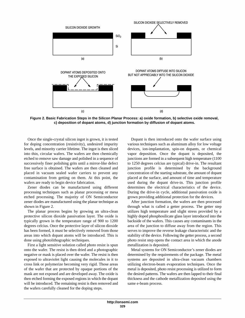
http://onsemi.com329
Figure 2. Basic Fabrication Steps in the Silicon Planar Process: a) oxide formation, b) selective oxide removal,c) deposition of dopant atoms, d) junction formation by diffusion of dopant atoms.
SILICON DIOXIDE GROWTH
SiO2
Si
(a)
SILICON DIOXIDE SELECTIVELY REMOVED
(b)
(c)
DOPANT ATOMS DEPOSITED ONTO
THE EXPOSED SILICON
(d)
DOPANT ATOMS DIFFUSE INTO SILICON
BUT NOT APPRECIABLY INTO THE SILICON DIOXIDE
Once the single-crystal silicon ingot is grown, it is testedfor doping concentration (resistivity), undesired impuritylevels, and minority carrier lifetime. The ingot is then slicedinto thin, circular wafers. The wafers are then chemicallyetched to remove saw damage and polished in a sequence ofsuccessively finer polishing grits until a mirror-like defectfree surface is obtained. The wafers are then cleaned andplaced in vacuum sealed wafer carriers to prevent anycontamination from getting on them. At this point, thewafers are ready to begin device fabrication.
Zener diodes can be manufactured using differentprocessing techniques such as planar processing or mesaetched processing. The majority of ON Semiconductorzener diodes are manufactured using the planar technique asshown in Figure 2.
The planar process begins by growing an ultra-cleanprotective silicon dioxide passivation layer. The oxide istypically grown in the temperature range of 900 to 1200degrees celcius. Once the protective layer of silicon dioxidehas been formed, it must be selectively removed from thoseareas into which dopant atoms will be introduced. This isdone using photolithographic techniques.
First a light sensitive solution called photo resist is spunonto the wafer. The resist is then dried and a photographicnegative or mask is placed over the wafer. The resist is thenexposed to ultraviolet light causing the molecules in it tocross link or polymerize becoming very rigid. Those areasof the wafer that are protected by opaque portions of themask are not exposed and are developed away. The oxide isthen etched forming the exposed regions in which the dopantwill be introduced. The remaining resist is then removed andthe wafers carefully cleaned for the doping steps.
Dopant is then introduced onto the wafer surface usingvarious techniques such as aluminum alloy for low voltagedevices, ion-implantation, spin-on dopants, or chemicalvapor deposition. Once the dopant is deposited, thejunctions are formed in a subsequent high temperature (1100to 1250 degrees celcius are typical) drive-in. The resultantjunction profile is determined by the backgroundconcentration of the starting substrate, the amount of dopantplaced at the surface, and amount of time and temperatureused during the dopant drive-in. This junction profiledetermines the electrical characteristics of the device.During the drive-in cycle, additional passivation oxide isgrown providing additional protection for the devices.
After junction formation, the wafers are then processedthrough what is called a getter process. The getter steputilizes high temperature and slight stress provided by ahighly doped phosphosilicate glass layer introduced into thebackside of the wafers. This causes any contaminants in thearea of the junction to diffuse away from the region. Thisserves to improve the reverse leakage characteristic and thestability of the device. Following the getter process, a secondphoto resist step opens the contact area in which the anodemetallization is deposited.
Metal systems for ON Semiconductor’s zener diodes aredetermined by the requirements of the package. The metalsystems are deposited in ultra-clean vacuum chambersutilizing electron-beam evaporation techniques. Once themetal is deposited, photo resist processing is utilized to formthe desired patterns. The wafers are then lapped to their finalthickness and the cathode metallization deposited using thesame e-beam process.

http://onsemi.com330
The quality of the wafers is closely monitored throughoutthe process by using statistical process control techniquesand careful microscopic inspections at critical steps. Specialwafer handling equipment is used throughout themanufacturing process to minimize contamination and toavoid damaging the wafers in any way. This furtherenhances the quality and stability of the devices.
Upon completion of the fabrication steps, the wafers areelectrically probed, inspected, and packaged for shipment tothe assembly operations. All ON Semiconductor zenerdiode product is sawn using 100% saw-through techniquesstringently developed to provide high quality silicon die.
ZENER DIODE ASSEMBLY
Surmetic 30, 40 and MOSORB
The plastic packages (Surmetic 30, 40 and MOSORBs)are assembled using oxygen free high conductivity copperleads for efficient heat transfer from the die and allowingmaximum power dissipation with a minimum of externalheatsinking. Figure 3 shows typical assembly. The leads areof nail head construction, soldered directly to the die, whichfurther enhances the heat dissipating capabilities of thepackage.
The Surmetic 30s, 40s and MOSORBs are basicallyassembled in the same manner; the only difference being theMOSORBs are soldered together using a solder discbetween the lead and die whereas the Surmetic 30s andSurmetic 40s utilize pre-soldered leads.
Assembly is started on the Surmetic 30 and 40 by loadingthe leads into assembly boats and pre-soldering the nailheads. After pre-soldering, one die is then placed into eachcavity of one assembly boat and another assembly boat isthen mated to it. Since the MOSORBs do not usepre-soldered leads, the leads are put into the assembly boat,
a solder disc is placed into each cavity and then a die is putin on top. A solder disc is put in on top of the die. Anotherassembly boat containing only leads is mated to the boatcontaining the leads, die, and two solder discs. The boats arepassed through the assembly furnace; this operation requiresonly one pass through the furnace.
After assembly, the leads on the Surmetic 30s, 40s andMOSORBs are plated with a tin-lead alloy making themreadily solderable and corrosion resistant.
Double Slug (DO-35 and DO-41)
Double slugs receive their name from the dumet slugs, oneattached to one end of each lead. These slugs sandwich thepre-tinned die between them and are hermetically sealed tothe glass envelope or body during assembly. Figure 4 showstypical assembly.
The assembly begins with the copper clad steel leadsbeing loaded into assembly “boats.” Every other boat loadof leads has a glass body set over the slug. A pre-tinned dieis placed into each glass body and the other boat load of leadsis mated to the boat holding the leads, body and die. Thesemated boats are then placed into the assembly furnace wherethe total mass is heated. Each glass body melts; and as theboat proceeds through the cooling portion of the furnacechamber, the tin which has wetted to each slug solidifiesforming a bond between the die and both slugs. The glasshardens, attaching itself to the sides of the two slugs formingthe hermetic seal. The above illustrates how the diodes arecompletely assembled using a single furnace passminimizing assembly problems.
The encapsulated devices are then processed through leadfinish. This consists of dipping the leads in molten tin/leadsolder alloy. The solder dipped leads produce an externalfinish which is tarnish-resistant and very solderable.
Figure 3. Double-Slug PlasticZener Construction
Figure 4. Double Slug GlassZener Construction
OFHC COPPER LEAD,
SOLDER PLATED
PLASTIC
(THERMO SET)
ENCAPSULATED
NAILHEAD LEAD
ZENER DIE Sn Pb
OFHC COPPER LEAD,
SOLDER PLATED
LEAD, STEEL, CU CLAD
SOLDER DIPPED
SLUG DUMET
GLASS SLEEVE
PASSIVATED
ZENER DIENAILHEAD LEAD

http://onsemi.com331
ZENER DIODE TEST, MARK AND PACKAGING
Double Slug, Surmetic 30, 40 and MOSORB
After lead finish, all products are final tested, whetherthey are double slug or of Surmetic construction, all are 100percent final tested for zener voltage, leakage current,impedance and forward voltage drop.
Process average testing is used which is based upon theaverages of the previous lots for a given voltage line andpackage type. Histograms are generated for the various
parameters as the units are being tested to ensure that the lotis testing well to the process average and compared againstother lots of the same voltage.
After testing, the units are marked as required by thespecification. The markers are equipped to polarity orientthe devices as well as perform 100% redundant test prior topackaging.
After marking, the units are packaged either in “bulk”form or taped and reeled or taped and ammo packed toaccommodate automatic insertion.

http://onsemi.com332
RELIABILITY
INTRODUCTION
ON Semiconductor’s Quality System maintains“continuous product improvement” goals in all phases of theoperation. Statistical process control (SPC), quality controlsampling, reliability audits and accelerated stress testingtechniques monitor the quality and reliability of its products.Management and engineering skills are continuouslyupgraded through training programs. This maintains aunified focus on Six Sigma quality and reliability from theinception of the product to final customer use.
STATISTICAL PROCESS CONTROL
ON Semiconductor’s Discrete Group is continuallypursuing new ways to improve product quality. Initial designimprovement is one method that can be used to produce asuperior product. Equally important to outgoing productquality is the ability to produce product that consistentlyconforms to specification. Process variability is the basicenemy of semiconductor manufacturing since it leads toproduct variability. Used in all phases ofON Semiconductor’s product manufacturing,STATISTICAL PROCESS CONTROL (SPC) replacesvariability with predictability. The traditional philosophy inthe semiconductor industry has been adherence to the datasheet specification. Using SPC methods assures the productwill meet specific process requirements throughout themanufacturing cycle. The emphasis is on defect prevention,not detection. Predictability through SPC methods requiresthe manufacturing culture to focus on constant andpermanent improvements. Usually these improvementscannot be bought with state-of-the-art equipment orautomated factories. With quality in design, process andmaterial selection, coupled with manufacturingpredictability, ON Semiconductor can produce world classproducts.
The immediate effect of SPC manufacturing ispredictability through process controls. Product centered anddistributed well within the product specification benefits ONSemiconductor with fewer rejects, improved yields and lowercost. The direct benefit to ON Semiconductor’s customersincludes better incoming quality levels, less inspection timeand ship-to-stock capability. Circuit performance is oftendependent on the cumulative effect of component variability.Tightly controlled component distributions give the customergreater circuit predictability. Many customers are alsoconverting to just-in-time (JIT) delivery programs. Theseprograms require improvements in cycle time and yieldpredictability achievable only through SPC techniques. Thebenefit derived from SPC helps the manufacturer meet thecustomer’s expectations of higher quality and lower costproduct.
Ultimately, ON Semiconductor will have Six Sigmacapability on all products. This means parametric
distributions will be centered within the specification limitswith a product distribution of plus or minus Six Sigma aboutmean. Six Sigma capability, shown graphically in Figure 1,details the benefit in terms of yield and outgoing qualitylevels. This compares a centered distribution versus a 1.5sigma worst case distribution shift.
New product development at ON Semiconductor requiresmore robust design features that make them less sensitive tominor variations in processing. These features make theimplementation of SPC much easier.
A complete commitment to SPC is present throughoutON Semiconductor. All managers, engineers, productionoperators, supervisors and maintenance personnel havereceived multiple training courses on SPC techniques.Manufacturing has identified 22 wafer processing and 8assembly steps considered critical to the processing of zenerproducts. Processes, controlled by SPC methods, that haveshown significant improvement are in the diffusion,photolithography and metallization areas.
To better understand SPC principles, brief explanationshave been provided. These cover process capability,implementation and use.
Figure 1. AOQL and Yield from a Normal Distribution ofProduct With 6 σ Capability
Standard Deviations From Mean
Distribution Centered Distribution Shifted ± 1.5At ± 3 σ 2700 ppm defective
99.73% yield
At ± 4 σ 63 ppm defective99.9937% yield
At ± 5 σ 0.57 ppm defective99.999943% yield
At ± 6 σ 0.002 ppm defective99.9999998% yield
66810 ppm defective93.32% yield
6210 ppm defective99.379% yield
233 ppm defective99.9767% yield
3.4 ppm defective99.99966% yield
6σ 5s 4σ 3σ 2σ 1σ 0 1σ 2σ 3σ 4σ 5σ 6σ
PROCESS CAPABILITY
One goal of SPC is to ensure a process is CAPABLE .Process capability is the measurement of a process toproduce products consistently to specificationrequirements. The purpose of a process capability study isto separate the inherent RANDOM VARIABILITY fromASSIGNABLE CAUSES. Once completed, steps are takento identify and eliminate the most significant assignablecauses. Random variability is generally present in thesystem and does not fluctuate. Sometimes, these areconsidered basic limitations associated with the machinery,materials, personnel skills or manufacturing methods.Assignable cause inconsistencies relate to time variations inyield, performance or reliability.

http://onsemi.com333
Figure 2. Impact of Assignable Causes on Process Predictable
Figure 3. Difference Between Process Control and Process Capability
??
?
??
?
???
Process “under control” – all assignable causes areremoved and future distribution is predictable.
PREDICTION
TIME
SIZESIZE
TIME
PREDICTION
SIZE
TIME
Out of control(assignable causes present)
In control assignable causes eliminated
SIZE
TIME
In control but not capable(variation from random variability
excessive)
LowerSpecification Limit
UpperSpecification Limit
In control and capable(variation from random
variability reduced)
? ?
Traditionally, assignable causes appear to be random dueto the lack of close examination or analysis. Figure 2 showsthe impact on predictability that assignable cause can have.Figure 3 shows the difference between process control andprocess capability.
A process capability study involves taking periodicsamples from the process under controlled conditions. Theperformance characteristics of these samples are chartedagainst time. In time, assignable causes can be identified andengineered out. Careful documentation of the process is keyto accurate diagnosis and successful removal of theassignable causes. Sometimes, the assignable causes willremain unclear requiring prolonged experimentation.
Elements which measure process variation control andcapability are Cp and Cpk respectively. Cp is thespecification width divided by the process width or Cp =(specification width) / 6σ. Cpk is the absolute value of theclosest specification value to the mean, minus the mean,divided by half the process width or Cpk = | closestspecification — X / 3σ.
At ON Semiconductor, for critical parameters, the processcapability is acceptable with a Cpk = 1.33. The desiredprocess capability is a Cpk = 2 and the ideal is a Cpk = 5.Cpk, by definition, shows where the current productionprocess fits with relationship to the specification limits. Offcenter distributions or excessive process variability willresult in less than optimum conditions.
SPC IMPLEMENTATION AND USE
The Discrete Group uses many parameters that showconformance to specification. Some parameters aresensitive to process variations while others remain constantfor a given product line. Often, specific parameters areinfluenced when changes to other parameters occur. It isboth impractical and unnecessary to monitor all parametersusing SPC methods. Only critical parameters that aresensitive to process variability are chosen for SPCmonitoring. The process steps affecting these criticalparameters must be identified also. It is equally important tofind a measurement in these process steps that correlateswith product performance. This is called a critical processparameter.
Once the critical process parameters are selected, a sampleplan must be determined. The samples used formeasurement are organized into RATIONALSUBGROUPS of approximately 2 to 5 pieces. Thesubgroup size should be such that variation among thesamples within the subgroup remain small. All samples mustcome from the same source e.g., the same mold pressoperator, etc.. Subgroup data should be collected atappropriate time intervals to detect variations in the process.As the process begins to show improved stability, theinterval may be increased. The data collected must becarefully documented and maintained for later correlation.Examples of common documentation entries would includeoperator, machine, time, settings, product type, etc..

http://onsemi.com334
Figure 4. Example of Process Control Chart Showing Oven Temperature Data
147
148
149
150
151
152
153
154
1 2 3 4 5 6 7 8 9 10 11 12 13 14 15 16 18 19 20 21 22 23 24 25 26 27 28 29 30 31 32 33 34 35 36 37 38 39 40 41 42 43 44 45 46 47 48 49 50 51 52 53 54 55 56 57 58 59 60 61 62 63 64 65 66 67 68 69 70 71 72 73 74 75
0
1
2
3
4
5
6
7
UCL = 152.8
= 150.4
LCL = 148.0
UCL = 7.3
= 3.2
LCL = 0
X
R
Once the plan is established, data collection may begin.The data collected will generate X and R values that areplotted with respect to time. X refers to the mean of thevalues within a given subgroup, while R is the range orgreatest value minus least value. When approximately 20 ormore X and R values have been generated, the average ofthese values is computed as follows:
X = (X + X2 + X3 + ...)/KR = (R1 + R2 + R3 + ...)/K
where K = the number of subgroups measured.The values of X and R are used to create the process
control chart. Control charts are the primary SPC tool usedto signal a problem. Shown in Figure 4, process controlcharts show X and R values with respect to time andconcerning reference to upper and lower control limitvalues. Control limits are computed as follows:
R upper control limit = UCLR = D4 RR lower control limit LCLR = D3 RX upper control limit = UCLX = X + A2 RX lower control limit = LCLX = X – A
Where D4, D3 and A2 are constants varying by samplesize, with values for sample sizes from 2 to 10 shown inthe following partial table:
Control charts are used to monitor the variability ofcritical process parameters. The R chart shows basic
problems with piece to piece variability related to theprocess. The X chart can often identify changes in people,machines, methods, etc. The source of the variability can bedifficult to find and may require experimental designtechniques to identify assignable causes.
Some general rules have been established to helpdetermine when a process is OUT-OF-CONTROL . Figure5a shows a control chart subdivided into zones A, B, and Ccorresponding to 3 sigma, 2 sigma, and 1 sigma limitsrespectively. In Figure 5b through Figure 5e four of the teststhat can be used to identify excessive variability and thepresence of assignable causes are shown. As familiarity witha given process increases, more subtle tests may beemployed successfully.
Once the variability is identified, the cause of thevariability must be determined. Normally, only a few factorshave a significant impact on the total variability of theprocess. The importance of correctly identifying thesefactors is stressed in the following example. Suppose aprocess variability depends on the variance of five factors A,B, C, D and E. Each has a variance of 5, 3, 2, 1 and 0.4respectively.Since:
σ tot = σA2 + σB2 + σC2 + σD2 + σE2
σ tot = 52 + 32 + 22 + 12 + (0.4)2 = 6.3
n 2 3 4 5 6 7 8 9 10
D4 3.27 2.57 2.28 2.11 2.00 1.92 1.86 1.82 1.78
D3 * * * * * 0.08 0.14 0.18 0.22
A2 1.88 1.02 0.73 0.58 0.48 0.42 0.37 0.34 0.31
* For sample sizes below 7, the LCLR would technically be a negative number; in those cases there is no lower control limit;this means that for a subgroup size 6, six “identical” measurements would not be unreasonable.

http://onsemi.com335
Now if only D is identified and eliminated then;
s tot = 52 + 32 + 22 + (0.4)2 = 6.2This results in less than 2% total variability improvement.
If B, C and D were eliminated, then;
σ tot = 52 + (0.4)2 = 5.02This gives a considerably better improvement of 23%. If
only A is identified and reduced from 5 to 2, then;
σ tot = 22 + 32 + 22 + 12 + (0.4)2 = 4.3Identifying and improving the variability from 5 to 2 gives
us a total variability improvement of nearly 40%.Most techniques may be employed to identify the primary
assignable cause(s). Out-of-control conditions may becorrelated to documented process changes. The product maybe analyzed in detail using best versus worst partcomparisons or Product Analysis Lab equipment.Multi-variance analysis can be used to determine the familyof variation (positional, critical or temporal). Lastly,experiments may be run to test theoretical or factorialanalysis. Whatever method is used, assignable causes must
be identified and eliminated in the most expeditious mannerpossible.
After assignable causes have been eliminated, newcontrol limits are calculated to provide a more challengingvariability criteria for the process. As yields and variabilityimprove, it may become more difficult to detectimprovements because they become much smaller. When allassignable causes have been eliminated and the pointsremain within control limits for 25 groups, the process issaid to be in a state of control.
SUMMARYON Semiconductor is committed to the use of
STATISTICAL PROCESS CONTROLS. These principles,used throughout manufacturing, have already resulted inmany significant improvements to the processes. Continueddedication to the SPC culture will allow ON Semiconductorto reach the Six Sigma and zero defect capability goals. SPCwill further enhance the commitment to TOTALCUSTOMER SATISFACTION .
UCL
LCL
UCL
UCLUCL
UCL
LCL
LCLLCL
LCL
CENTERLINE
A
B
C
C
B
A
A
B
C
C
B
A
A
B
C
C
B
A
A
B
C
C
B
A
ZONE A (+ 3 SIGMA)
ZONE B (+ 2 SIGMA)
ZONE C (+ 1 SIGMA)
ZONE C (– 1 SIGMA)
ZONE B (– 2 SIGMA)
ZONE A (– 3 SIGMA)
Figure 5a. Control Chart Zones Figure 5b. One Point Outside Control LimitIndicating Excessive Variability
Figure 5c. Two Out of Three Points in Zone A orBeyond Indicating Excessive Variability
Figure 5d. Four Out of Five Points in Zone B orBeyond Indicating Excessive Variability
Figure 5e. Seven Out of Eight Points in Zone C orBeyond Indicating Excessive Variability

http://onsemi.com336
RELIABILITY STRESS TESTS
The following gives brief descriptions of the reliabilitytests commonly used in the reliability monitoring program.Not all of the tests listed are performed on each product.Other tests may be performed when appropriate. In additionsome form of preconditioning may be used in conjunctionwith the following tests.
AUTOCLAVE (aka, PRESSURE COOKER)
Autoclave is an environmental test which measuresdevice resistance to moisture penetration and the resultanteffects of galvanic corrosion. Autoclave is a highlyaccelerated and destructive test.
Typical Test Conditions: TA = 121°C, rh = 100%, p =1 atmosphere (15 psig), t = 24 to 96 hoursCommon Failure Modes: Parametric shifts, highleakage and/or catastrophicCommon Failure Mechanisms: Die corrosion orcontaminants such as foreign material on or within thepackage materials. Poor package sealing
HIGH HUMIDITY HIGH TEMPERATURE BIAS(H3TB or H3TRB)
This is an environmental test designed to measure themoisture resistance of plastic encapsulated devices. A biasis applied to create an electrolytic cell necessary toaccelerate corrosion of the die metallization. With time, thisis a catastrophically destructive test.
Typical Test Conditions: TA = 85°C to 95°C, rh = 85%to 95%, Bias = 80% to 100% of Data Book max. rating,t = 96 to 1750 hoursCommon Failure Modes: Parametric shifts, highleakage and/or catastrophicCommon Failure Mechanisms: Die corrosion orcontaminants such as foreign material on or within thepackage materials. Poor package sealingMilitary Reference: MIL-STD-750, Method 1042
HIGH TEMPERATURE REVERSE BIAS (HTRB)
The purpose of this test is to align mobile ions by meansof temperature and voltage stress to form a high-currentleakage path between two or more junctions.
Typical Test Conditions: TA = 85°C to 150°C, Bias =80% to 100% of Data Book max. rating, t = 120 to 1000hoursCommon Failure Modes: Parametric shifts in leakageCommon Failure Mechanisms: Ionic contamination onthe surface or under the metallization of the dieMilitary Reference: MIL-STD-750, Method 1039
HIGH TEMPERATURE STORAGE LIFE (HTSL)
High temperature storage life testing is performed toaccelerate failure mechanisms which are thermallyactivated through the application of extreme temperatures.
Typical Test Conditions: TA = 70°C to 200°C, no bias,t = 24 to 2500 hoursCommon Failure Modes: Parametric shifts in leakageCommon Failure Mechanisms: Bulk die and diffusiondefectsMilitary Reference: MIL-STD-750, Method 1032
INTERMITTENT OPERATING LIFE (IOL)
The purpose of this test is the same as SSOL in additionto checking the integrity of both wire and die bonds bymeans of thermal stressing.
Typical Test Conditions: TA = 25°C, Pd = Data Bookmaximum rating, Ton = Toff = ∆ of 50°C to 100°C, t =42 to 30000 cyclesCommon Failure Modes: Parametric shifts andcatastrophicCommon Failure Mechanisms: Foreign material, crackand bulk die defects, metallization, wire and die bonddefectsMilitary Reference: MIL-STD-750, Method 1037
MECHANICAL SHOCK
This test is used to determine the ability of the device towithstand a sudden change in mechanical stress due toabrupt changes in motion as seen in handling, transportation,or actual use.
Typical Test Conditions: Acceleration = 1500 g’s,Orientation = X1, Y1, Y2 plane, t = 0.5 msec, Blows = 5Common Failure Modes: Open, short, excessiveleakage, mechanical failureCommon Failure Mechanisms: Die and wire bonds,cracked die, package defectsMilitary Reference: MIL-STD-750, Method 2015
MOISTURE RESISTANCE
The purpose of this test is to evaluate the moistureresistance of components under temperature/humidityconditions typical of tropical environments.
Typical Test Conditions: TA = –10°C to 65°C, rh = 80%to 98%, t = 24 hours/cycle, cycle = 10Common Failure Modes: Parametric shifts in leakageand mechanical failureCommon Failure Mechanisms: Corrosion orcontaminants on or within the package materials. Poorpackage sealingMilitary Reference: MIL-STD-750, Method 1021

http://onsemi.com337
SOLDERABILITY
The purpose of this test is to measure the ability of deviceleads/terminals to be soldered after an extended period ofstorage (shelf life).
Typical Test Conditions: Steam aging = 8 hours, Flux= R, Solder = Sn60, Sn63Common Failure Modes: Pin holes, dewetting,non-wettingCommon Failure Mechanisms: Poor plating,contaminated leadsMilitary Reference: MIL-STD-750, Method 2026
SOLDER HEAT
This test is used to measure the ability of a device towithstand the temperatures as may be seen in wave solderingoperations. Electrical testing is the endpoint criterion for thisstress.
Typical Test Conditions: Solder Temperature = 260°C,t = 10 secondsCommon Failure Modes: Parameter shifts, mechanicalfailureCommon Failure Mechanisms: Poor package designMilitary Reference: MIL-STD-750, Method 2031
STEADY STATE OPERATING LIFE (SSOL)
The purpose of this test is to evaluate the bulk stability ofthe die and to generate defects resulting from manufacturingaberrations that are manifested as time and stress-dependentfailures.
Typical Test Conditions: TA = 25°C, PD = Data Bookmaximum rating, t = 16 to 1000 hoursCommon Failure Modes: Parametric shifts andcatastrophicCommon Failure Mechanisms: Foreign material, crackdie, bulk die, metallization, wire and die bond defectsMilitary Reference: MIL-STD-750, Method 1026
TEMPERATURE CYCLING (AIR TO AIR)
The purpose of this test is to evaluate the ability of thedevice to withstand both exposure to extreme temperatures
and transitions between temperature extremes. This testingwill also expose excessive thermal mismatch betweenmaterials.
Typical Test Conditions: TA = –65°C to 200°C, cycle= 10 to 1000Common Failure Modes: Parametric shifts andcatastrophicCommon Failure Mechanisms: Wire bond, cracked orlifted die and package failureMilitary Reference: MIL-STD-750, Method 1051
THERMAL SHOCK (LIQUID TO LIQUID)
The purpose of this test is to evaluate the ability of thedevice to withstand both exposure to extreme temperaturesand sudden transitions between temperature extremes. Thistesting will also expose excessive thermal mismatchbetween materials.
Typical Test Conditions: TA = 0°C to 100°C, cycles= 10 to 1000Common Failure Modes: Parametric shifts andcatastrophicCommon Failure Mechanisms: Wire bond, cracked orlifted die and package failureMilitary Reference: MIL-STD-750, Method 1056
VARIABLE FREQUENCY VIBRATION
This test is used to examine the ability of the device towithstand deterioration due to mechanical resonance.
Typical Test Conditions: Peak acceleration = 20 g’s,Frequency range = 20 Hz to 20 kHz, t = 48 minutes.Common Failure Modes: Open, short, excessiveleakage, mechanical failureCommon Failure Mechanisms: Die and wire bonds,cracked die, package defectsMilitary Reference: MIL-STD-750, Method 2056

http://onsemi.com338
ZENER DIODE CHARACTERISTICS
INTRODUCTION
At first glance the zener diode is a simple deviceconsisting of one P-N junction with controlled breakdownvoltage properties. However, when considerations are givento the variations of temperature coefficient, zenerimpedance, thermal time response, and capacitance, all ofwhich are a function of the breakdown voltage (from 1.8 to400 V), a much more complicated picture arises. In additionto the voltage spectrum, a variety of power packages are onthe market with a variation of dice area inside theencapsulation.
This chapter is devoted to sorting out the importantconsiderations in a “typical” fashion. For exact details, thedata sheets must be consulted. However, much of theinformation contained herein is supplemental to the datasheet curves and will broaden your understanding of zenerdiode behavior.
Specifically, the following main subjects will be detailed:
Basic DC Volt-Ampere CharacteristicsImpedance versus Voltage and CurrentTemperature Coefficient versus Voltage and CurrentPower DeratingMountingThermal Time Response – Effective Thermal ImpedanceSurge CapabilitiesFrequency Response – Capacitance and Switching
Effects
BASIC ZENER DIODE DC VOLT-AMPERECHARACTERISTICS
Reverse and forward volt-ampere curves are representedin Figure 1 for a typical zener diode. The three areas –forward, leakage, and breakdown – will each be examined.
FORWARD DC CHARACTERISTICS
The forward characteristics of a zener diode areessentially identical with an “ordinary” rectifier and isshown in Figure 2. The volt-ampere curve follows the basicdiode equation of IF = IReqV/KT where KT/q equals about0.026 volts at room temperature and IR (reverse leakagecurrent) is dependent upon the doping levels of the P-Njunction as well as the area. The actual plot of VF versus IFdeviates from the theoretical due to slightly “fixed” seriesresistance of the lead wire, bonding contacts and some bulkeffects in the silicon.
Figure 1. Typical Zener Diode DC V-I Characteristics(Not to Scale)
FORWARD VOLTAGE
REVERSE VOLTAGE
BREAKDOWNREGION
LEAKAGE REGION
FORWARD CHARACTERISTIC
FO
RW
AR
D C
UR
RE
NT
RE
VE
RS
E C
UR
RE
NT
While the common form of the diode equation suggeststhat IR is constant, in fact IR is itself strongly temperaturedependent. The rapid increase in IR with increasingtemperature dominates the decrease contributed by theexponential term in the diode equation. As a result, theforward current increases with increasing temperature.Figure 2 shows a forward characteristic temperaturedependence for a typical zener. These curves indicate thatfor a constant current, an increase in temperature causes adecrease in forward voltage. The voltage temperaturecoefficient values are typically in the range of –1.4 to–2 mV/°C.
Figure 2. Typical Forward Characteristics ofZener Diodes
10.90.80.70.60.50.40.3
1000
VF, FORWARD VOLTAGE (VOLTS)
500
200
100
50
20
10
5
2
1
I ,
FO
RW
AR
D C
UR
RE
NT
(mA
)F
TJ = 150°C 100°C 25°C -55°C

http://onsemi.com339
LEAKAGE DC CHARACTERISTICS
When reverse voltage less than the breakdown is appliedto a zener diode, the behavior of current is similar to anyback-biased silicon P-N junction. Ideally, the reverse currentwould reach a level at about one volt reverse voltage andremain constant until breakdown is reached. There are boththeoretical and practical reasons why the typical V-I curvewill have a definite slope to it as seen in Figure 3.Multiplication effects and charge generation sites arepresent in a zener diode which dictate that reverse current(even at low voltages) will increase with voltage. Inaddition, surface charges are ever present across P-Njunctions which appear to be resistive in nature.
The leakage currents are generally less than onemicroampere at 150°C except with some large area devices.Quite often a leakage specification at 80% or so ofbreakdown voltage is used to assure low reverse currents.
Figure 3. Typical Leakage Currentversus Voltage
2016126400.1
1
10
100
1000
10000
I ,
RE
VE
RS
E L
EA
KA
GE
CU
RR
EN
T (n
A)
R
VR, REVERSE VOLTAGE (VOLTS)
TJ = 150°C
25°C
-55°C
VOLTAGE BREAKDOWN
At some definite reverse voltage, depending on the dopinglevels (resistivity) of the P-N junction, the current will beginto avalanche. This is the so-called “zener” or “breakdown”area and is where the device is usually biased during use. Atypical family of breakdown curves showing the effect oftemperature is illustrated in Figure 4.
Between the minimum currents shown in Figure 4 and theleakage currents, there is the “knee” region. The avalanchemechanism may not occur simultaneously across the entirearea of the P-N junction, but first at one microscopic site,then at an increasing number of sites as further voltage isapplied. This action can be accounted for by the“microplasma discharge” theory and correlates with severalbreakdown characteristics.
Figure 4. Typical Zener CharacteristicVariation with Temperature
32313029282726250.10.2
0.5
12
5
1020
50
100
200
5001000
VZ, ZENER VOLTAGE (VOLTS)
I ,
ZE
NE
R C
UR
RE
NT
(mA
)Z
T = -55°C 100°C25°C 150°C
T = TJT = TA
An exaggerated view of the knee region is shown inFigure 5. As can be seen, the breakdown or avalanchecurrent does not increase suddenly, but consists of a seriesof smoothly rising current versus voltage increments eachwith a sudden break point.
Figure 5. Exaggerated V-I Characteristicsof the Knee Region
EXAGGERATED VI
OF KNEE REGION
ZENER VOLTAGE
VOLTAGE
ZE
NE
R C
UR
RE
NT
CU
RR
EN
T
At the lowest point, the zener resistance (slope of thecurve) would test high, but as current continues to climb, theresistance decreases. It is as though each discharge site hashigh resistance with each succeeding site being in paralleluntil the total resistance is very small.
In addition to the resistive effects, the micro plasmas mayact as noise generators. The exact process of manufacturingaffects how high the noise will be, but in any event there willbe some noise at the knee, and it will diminish considerablyas current is allowed to increase.
Since the zener impedance and the temperaturecoefficient are of prime importance when using the zenerdiode as a reference device, the next two sections willexpand on these points.

http://onsemi.com340
ZENER IMPEDANCE
The slope of the VZ – IZ curve (in breakdown) is definedas zener impedance or resistance. The measurement isgenerally done with a 60 Hz (on modern, computerizedequipment this test is being done at 1 kHz) current variationwhose value is 10% in rms of the dc value of the current.(That is, ∆IZ peak to peak = 0.282 IZ.) This is really not asmall signal measurement but is convenient to use and givesrepeatable results.
The zener impedance always decreases as currentincreases, although at very high currents (usually beyond IZmax) the impedance will approach a constant. In contrast,the zener impedance decreases very rapidly with increasingcurrent in the knee region. On Semiconductor specifies mostzener diode impedances at two points: IZT and IZK. The termIZT usually is at the quarter power point, and IZK is anarbitrary low value in the knee region. Between these twopoints a plot of impedance versus current on a log-log scaleis close to a straight line. Figure 6 shows a typical plot of ZZversus IZ for a 20 volt–500 mW zener. The worst caseimpedance between IZT and IZK could be approximated byassuming a straight line function on a log-log plot; however,at currents above IZT or below IZK a projection of this linemay give erroneous values.
Figure 6. Zener Impedance versusZener Current
ZENER CURRENT (mA)
1001010.11
10
100
1000
ZE
NE
R IM
PE
DA
NC
E (
OH
MS
) APPROXIMATE MAXIMUM LINE
ZZT(MAX)
ZZK(MAX)
The impedance variation with voltage is much morecomplex. First of all, zeners below 6 volts or so exhibit “fieldemission” breakdown converting to “avalanche” at highercurrents. The two breakdowns behave somewhat differentlywith “field emission” associated with high impedance andnegative temperature coefficients and “avalanche” withlower impedance and positive temperature coefficients.
A V-I plot of several low voltage 500 mW zener diodes isshown in Figure 7. It is seen that at some given current(higher for the lower voltage types) there is a fairly suddendecrease in the slope of ∆V/∆I. Apparently, this current is thetransition from one type of breakdown to the other. Above6 volts the curves would show a gradual decrease of ∆V/∆Irather than an abrupt change, as current is increased.
Figure 7. Zener Current versus Zener Voltage(Low Voltage Region)
1
100
10
1
0.1
0.012 3 4 5 6 7 8
ZENER VOLTAGE (VOLTS)
ZE
NE
R C
UR
RE
NT
(mA
)
Possibly the plots shown in Figure 8 of zener impedanceversus voltage at several constant IZ’s more clearly pointsout this effect. It is obvious that zener diodes whosebreakdowns are about 7 volts will have remarkably lowimpedance.
20010070503020107532
1 mA
10 mA
20 mA
Figure 8. Dynamic Zener Impedance (Typical)versus Zener Voltage
2
3
57
10
20
30
5070
100
200Z
, D
YN
AM
IC IM
PE
DA
NC
E (
OH
MS
)Z
VZ, ZENER VOLTAGE (VOLTS)
TA = 25°C
IZ(ac) = 0.1 IZ(dc)
However, this is not the whole picture. A zener diodefigure of merit as a regulator could be ZZ/VZ. This wouldgive some idea of what percentage change of voltage couldbe expected for some given change in current. Of course, alow ZZ/VZ is desirable. Generally zener current must bedecreased as voltage is increased to prevent excessive powerdissipation; hence zener impedance will rise even higher andthe “figure of merit” will become higher as voltageincreases. This is the case with IZT taken as the test point.However, if IZK is used as a comparison level in thosedevices which keep a constant IZK over a large range ofvoltage, the “figure of merit” will exhibit a bowl-shapedcurve – first decreasing and then increasing as voltage isincreased. Typical plots are shown in Figure 9. Theconclusion can be reached that for uses where wide swingsof current may occur and the quiescent bias current must behigh, the lower voltage zener will provide best regulation,
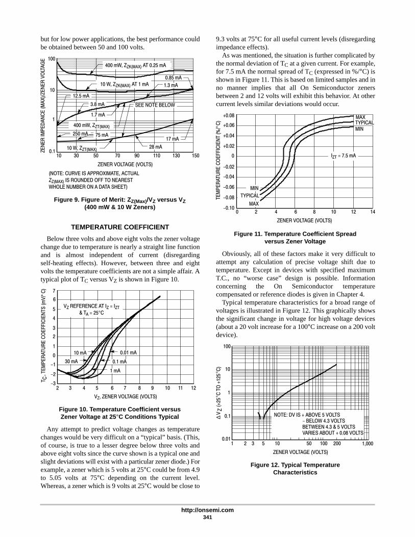
http://onsemi.com341
but for low power applications, the best performance couldbe obtained between 50 and 100 volts.
703010 50 90 110 130 150
0.85 mA
17 mA250 mA
10 W, ZZT(MAX)
1.7 mA
SEE NOTE BELOW
1.3 mA
12.5 mA
3.8 mA
28 mA
75 mA
ZENER VOLTAGE (VOLTS)
ZE
NE
R IM
PE
DA
NC
E (
MA
X)/
ZE
NE
R V
OLT
AG
E
10
100
1
0.1
(NOTE: CURVE IS APPROXIMATE, ACTUAL
ZZ(MAX) IS ROUNDED OFF TO NEAREST
WHOLE NUMBER ON A DATA SHEET)
Figure 9. Figure of Merit: Z Z(Max)/VZ versus V Z(400 mW & 10 W Zeners)
400 mW, ZZK(MAX) AT 0.25 mA
10 W, ZZK(MAX) AT 1 mA
400 mW, ZZT(MAX)
TEMPERATURE COEFFICIENT
Below three volts and above eight volts the zener voltagechange due to temperature is nearly a straight line functionand is almost independent of current (disregardingself-heating effects). However, between three and eightvolts the temperature coefficients are not a simple affair. Atypical plot of TC versus VZ is shown in Figure 10.
2 3 4 5 6 7 8 9 11
0.01 mA
0.1 mA30 mA
1 mA
10 mA
Figure 10. Temperature Coefficient versusZener Voltage at 25 °C Conditions Typical
7
6
5
4
3
2
1
0
-1
-2
-3
VZ, ZENER VOLTAGE (VOLTS)
10 12
T
, TE
MP
ER
ATU
RE
CO
EF
FIC
IEN
TS
(m
V/
C)
C°
VZ REFERENCE AT IZ = IZT
& TA = 25°C
Any attempt to predict voltage changes as temperaturechanges would be very difficult on a “typical” basis. (This,of course, is true to a lesser degree below three volts andabove eight volts since the curve shown is a typical one andslight deviations will exist with a particular zener diode.) Forexample, a zener which is 5 volts at 25°C could be from 4.9to 5.05 volts at 75°C depending on the current level.Whereas, a zener which is 9 volts at 25°C would be close to
9.3 volts at 75°C for all useful current levels (disregardingimpedance effects).
As was mentioned, the situation is further complicated bythe normal deviation of TC at a given current. For example,for 7.5 mA the normal spread of TC (expressed in %/°C) isshown in Figure 11. This is based on limited samples and inno manner implies that all On Semiconductor zenersbetween 2 and 12 volts will exhibit this behavior. At othercurrent levels similar deviations would occur.
+0.08
+0.06
+0.04
+0.02
0
-0.02
-0.08
-0.10
-0.04
-0.06
0 2 4 6 8 10 12 14
ZENER VOLTAGE (VOLTS)
TYPICAL
MAX
Figure 11. Temperature Coefficient Spreadversus Zener Voltage
TE
MP
ER
ATU
RE
CO
EF
FIC
IEN
T (%
/C
)°
MAX
MIN
MIN
TYPICAL
IZT = 7.5 mA
Obviously, all of these factors make it very difficult toattempt any calculation of precise voltage shift due totemperature. Except in devices with specified maximumT.C., no “worse case” design is possible. Informationconcerning the On Semiconductor temperaturecompensated or reference diodes is given in Chapter 4.
Typical temperature characteristics for a broad range ofvoltages is illustrated in Figure 12. This graphically showsthe significant change in voltage for high voltage devices(about a 20 volt increase for a 100°C increase on a 200 voltdevice).
NOTE: DV IS + ABOVE 5 VOLTS- BELOW 4.3 VOLTSBETWEEN 4.3 & 5 VOLTSVARIES ABOUT + 0.08 VOLTS
ZENER VOLTAGE (VOLTS)
1 2 3 5 10 50 100 200 1,000
100
10
1
0.1
Figure 12. Typical TemperatureCharacteristics
V
(+2
5 C
TO
+12
5 C
)°
°∆
Z
0.01

http://onsemi.com342
POWER DERATING AND MOUNTING
The zener diode like any other semiconductor has amaximum junction temperature. This limit is somewhatarbitrary and is set from a reliability viewpoint. Mostsemiconductors exhibit an increasing failure rate astemperature increases. At some temperature, the solder willmelt or soften and the failure rate soars. The 175°C to 200°Cjunction temperature rating is quite safe from solder failuresand still has a very low failure rate.
In order that power dissipated in the device will never causethe junction to rise beyond 175°C or 200°C (depending on thedevice), the relation between temperature rise and powermust be known. Of course, the thermal resistance (RθJA orRθJL) is the factor which relates power and temperature in thewell known “Thermal Ohm’s Law’’ relation:
∆T = TJ – TA = RθJAPZ (1)and
∆T = TJ – TL = RθJLPZ (2)where
TJTATLRθJARθJLPZ
= Junction temperature= Ambient temperature= Lead temperature= Thermal resistance junction to ambient= Thermal resistance junction to lead= Zener power dissipation
Obviously, if ambient or lead temperature is known andthe appropriate thermal resistance for a given device isknown, the junction temperature could be preciselycalculated by simply measuring the zener dc current andvoltage (PZ = IZVZ). This would be helpful to calculatevoltage change versus temperature. However, onlymaximum and typical values of thermal resistance are givenfor a family of zener diodes. So only “worst case” or typicalinformation could be obtained as to voltage changes.
The relations of equations 1 and 2 are usually expressedas a graphical derating of power versus the appropriatetemperature. Maximum thermal resistance is used togenerate the slope of the curve. An example of a 400milliwatt device derated to the ambient temperature and a 1watt device derated to the lead temperature are shown inFigures 13 and 14.
500
25 50 75 100 125 150 175 200
400
300
200
100
0
TA, AMBIENT TEMPERATURE (°C)
Figure 13. 400 mW Power TemperatureDerating Curve
P
, PO
WE
R D
ISS
IPA
TIO
N (
MIL
LIW
AT
TS
)D
1.25
0 20 40 60 80 100 120 140 160 180 200
L = LEAD LENGTH
TO HEAT SINK1
0.75
0.50
0.25
L = 1/8″L = 3/8″
L = 1″
TL, LEAD TEMPERATURE (°C)
Figure 14. Power TemperatureDerating Curve
P
, MA
XIM
UM
PO
WE
R D
ISS
IPA
TIO
N (
WA
TT
S)
D
A lead mounted device can have its power ratingincreased by shortening the lead length and “heatsinking”the ends of the leads. This effect is shown in Figure 15, forthe 1N4728, 1 watt zener diode.
Each zener has a derating curve on its data sheet andsteady state power can be set properly. However,temperature increases due to pulse use are not so easilycalculated. The use of “Transient Thermal Resistance”would be required. The next section expounds upontransient thermal behavior as a function of time and surgepower.
175
0
150
125
100
75
50
25
00.1 0.2 0.3 0.4 0.5 0.6 0.7 0.8 0.9 1
L, LEAD LENGTH TO HEAT SINK (INCH)
Figure 15. Typical 1N4728 ThermalResistance versus Lead Length
R
JL, J
UN
CT
ION
-TO
-LE
AD
TH
ER
MA
L R
ES
ISTA
NC
E (°C
/W)
THERMAL TIME RESPONSE
Early studies of zener diodes indicated that a “thermaltime constant” existed which allowed calculation oftemperature rise as a function of power pulse height, width,and duty cycle. More precise measurements have shown thattemperature response as a function of time cannot berepresented as a simple time constant. Although as shown inthe preceding section, the steady state conditions areanalogous in every way to an electrical resistance; a simple“thermal capacitance” placed across the resistor is not thetrue equivalent circuit. Probably a series of parallel R-C

http://onsemi.com343
networks or lumped constants representing a thermaltransmission line would be more accurate.
Fortunately a concept has developed in the industrywherein the exact thermal equivalent circuit need not befound. If one simply accepts the concept of a thermalresistance which varies with time in a predictable manner,the situation becomes very practical. For each family ofzener diodes, a “worst case” transient thermal resistancecurve may be generated.
The main use of this transient RθJL curve is when the zeneris used as a clipper or a protective device. First of all, thepower wave shape must be constructed. (Note, even thoughthe power-transient thermal resistance indicates reasonablejunction temperatures, the device still may fail if the peakcurrent exceeds certain values. Apparently a currentcrowding effect occurs which causes the zener to short. Thisis discussed further in this section.)
TRANSIENT POWER-TEMPERATURE EFFECTS
A typical transient thermal resistance curve is shown inFigure 16. This is for a lead mounted device and shows theeffect of lead length to an essentially infinite heatsink.
To calculate the temperature rise, the power surge waveshape must be approximated by its rectangular equivalent asshown in Figure 17. In case of an essentially non-recurrentpulse, there would be just one pulse, and ∆T = RθT1 Pp. Inthe general case, it can be shown that
whereDRθT1
RθT
RθT1 + T
RθJA(ss) or RθJL(ss) = Steady state value of thermalRθJA(ss) or RθJL(ss) = resistance
= Duty cycle in percent= Transient thermal resistance at the time
equal to the pulse width= Transient thermal resistance at the time
equal to pulse interval= Transient thermal resistance at the time
equal to the pulse interval= plus one more pulse width.
∆T = [DRθJA (ss) + (1 – D) RθT1 + T + RθT1 – RθT] PP
PW, PULSE WIDTH (ms)
100
3 5 10 20 50 100 200 500 1000 2000 5000 10k 30k
70
50
30
20
10
7
5
3
2
1
L = 1/32″
L = 1″
FOR θJL(t) VALUES AT PULSE WIDTHSLESS THAN 3.0 ms, THE ABOVECURVE CAN BE EXTRAPOLATEDDOWN TO 10 µs AT A CONTINUINGSLOPE OF 1/2
Figure 16. Typical Transient ThermalResistance (For Axial Lead Zener)
L L
HEAT SINKÉÉÉÉ
ÉÉÉÉ
TH
ER
MA
L R
ES
ISTA
NC
E (
C/W
)°
RJL
(t),
JUN
CT
ION
TO
LE
AD
TR
AN
SIE
NT
θ
Figure 17. Relation of Junction Temperature toPower Pulses
T
T1T1
T
PEAKTEMPERATURE RISE
AVERAGETEMPERATURE RISE
AMBIENTTEMPERATURE
PEAK POWER (PP)
AVERAGE POWER = PP
This method will predict the temperature rise at the end ofthe power pulse after the chain of pulses has reachedequilibrium. In other words, the average power will havecaused an average temperature rise which has stabilized, buta temperature “ripple” is present.
Example: (Use curve in Figure 16)PP = 5 watt (Lead length 1/32″)D = 0.1T1 = 10 msT = 100 msRθJA(ss) = 12°C/W (for 1/32″ lead length)
ThenRθT1 = 1.8°C/WRθT = 5.8°C/WRθT1 + T = 6°C/W
And∆T = [0.1 x 12 + (1 – 0.1) 6 + 1.8 – 5.8] 5∆T = 13°C
Or at TA = 25°, TJ = 38°C peak
SURGE FAILURES
If no other considerations were present, it would be asimple matter to specify a maximum junction temperatureno matter what pulses are present. However, as has beennoted, apparently other fault conditions prevail. The samegroup of devices for which the transient thermal curves weregenerated were tested by subjecting them to single shotpower pulses. A failure was defined as a significant shift ofleakage or zener voltage, or of course opens or shorts. Eachdevice was measured before and after the applied pulse.Most failures were shifts in zener voltage. The results areshown in Figure 18.
Attempts to correlate this to the transient thermalresistance work quite well on a typical basis. For example,assuming a value for 1 ms of 90 watts and 35 watts at 10 ms,the predicted temperature rise would be 180°C and 190°C.But on a worst case basis, the temperature rises would beabout one half these values or junction temperatures, on theorder of 85°C to 105°C, which are obviously low.Apparently at very high power levels a current restrictionoccurs causing hot spots. There was no apparent correlation

http://onsemi.com344
of zener voltage or current on the failure points since eachgroup of failures contained a mixture of voltages.
1000
0.00001 0.0001 0.001 0.01 0.1 1
WORSE CASE
100
10
1
PO
WE
R (
WA
TT
S)
Figure 18. One Shot Power Failure AxialLead Zener Diode
TIME OF PULSE (SECONDS)
TYPICAL
VOLTAGE VERSUS TIME
Quite often the junction temperature is only of academicinterest, and the designer is more concerned with the voltagebehavior versus time. By using the transient thermalresistance, the power, and the temperature coefficient, thedesigner could generate VZ versus time curves. TheOn Semiconductor zener diode test group has observeddevice voltages versus time until the thermal equilibriumwas reached. A typical curve is shown for a lead mountedlow wattage device in Figure 19 where the ambienttemperature was maintained constant. It is seen that voltagestabilizes in about 100 seconds for 1 inch leads.
Since information contained in this section may not befound on data sheets it is necessary for the designer tocontact the factory when using a zener diode as a surgesuppressor. Additional information on transient suppressionapplication is presented elsewhere in this book.
166
0.01
165
164
163
162
161
1600.1 1 10 100
TIME (SECONDS)
ZE
NE
R V
OLT
AG
E (
VO
LTS
)
Figure 19. Zener Voltage (Typical) versusTime for Step Power Pulses
(500 mW Lead Mounted Devices)
FREQUENCY AND PULSE CHARACTERISTICS
The zener diode may be used in applications whichrequire a knowledge of the frequency response of the device.Of main concern are the zener resistance (usually specifiedas “impedance”) and the junction capacitance. Thecapacitance curves shown in this section are typical.
ZENER CAPACITANCE
Since zener diodes are basically PN junctions operated inthe reverse direction, they display a capacitance thatdecreases with increasing reverse voltage. This is so becausethe effective width of the PN junction is increased by theremoval of charges (holes and electrons) as reverse voltageis increased. This decrease in capacitance continues until thezener breakdown region is entered; very little furthercapacitance change takes place, owing to the now fixedvoltage across the junction. The value of this capacitance isa function of the material resistivity, ρ, (amount of doping –which determines VZ nominal), the diameter, D, of junctionor dice size (determines amount of power dissipation), thevoltage across the junction VC, and some constant, K. Thisrelationship can be expressed as:
KD4pVC
CC =n KD4
ρVC
After the junction enters the zener region, capacitanceremains relatively fixed and the AC resistance thendecreases with increasing zener current.
TEST CIRCUIT CONSIDERATIONS: A capacitivebridge was used to measure junction capacitance. In thismethod the zener is used as one leg of a bridge that isbalanced for both DC at a given reverse voltage and for AC(the test frequency 1 MHz). After balancing, the variablecapacitor used for balancing is removed and its valuemeasured on a test instrument. The value thus indicated isthe zener capacitance at reverse voltage for which bridgebalance was obtained. Figure 20 shows capacitance testcircuit.
Figure 21 is a plot of junction capacitance for diffusedzener diode units versus their nominal operating voltage.Capacitance is the value obtained with reverse bias set atone-half the nominal VZ. The plot of the voltage range from6.8 V to 200 V, for three dice sizes, covers mostOn Semiconductor diffused-junction zeners. Consultspecific data sheets for capacitance values.
Figures 22, 23, and 24 show plots of capacitance versusreverse voltage for units of various voltage ratings in eachof the three dice sizes. Junction capacitance decreases asreverse voltage increases to the zener region. This change incapacitance can be expressed as a ratio which follows aone-third law, and C1/C2 = (V2/V1)1/3. This law holds onlyfrom the zener voltage down to about 1 volt, where the curvebegins to flatten out. Figure 25 shows this for a group of lowwattage units.

http://onsemi.com345
Figure 20. Capacitance Test Circuit
C1
C2
VDC1 k1% 1 k
1%
1 k
1%
1 k1%
DC
POWER
SUPPLY
HP
NO. 712A
100 W
IV
VAC
1 MHz
SIGNAL
GEN
TEK
NO. 190A
10/50
pF
XZENER
UNDER
TEST
HIGAIN
DIFF SCOPE
NULL IND
TEK
TYPE D
R = ZR R
CAP
DECADE
0-.09 mF
100 pF
STEPS
∆C 1%
BAL READ
S1
10/150pF
L/C
METER
TEK
140
0.1 µF
1,000
1 10 100
VR, REVERSE VOLTAGE (VOLTS)
100
10
C
, CA
PAC
ITA
NC
E (
PIC
OFA
RA
DS
)Z
100 VOLTS
50 VOLTS
20 VOLTS
10 VOLTS
10,000
1 10 100 1,000
1,000
100
10C
, CA
PAC
ITA
NC
E (
PIC
OFA
RA
DS
) @
VZ
/ 2
VZ, NOMINAL UNIT VOLTAGE (VOLTS)
Z
HIGH WATTAGE
LOW WATTAGE
MEDIUM WATTAGE
Figure 21. Capacitance versus Voltage Figure 22. Capacitance versus Reverse Voltage
LOW WATTAGE UNITS
AVG. FOR 10 UNITS EACH
10,000
1 10
VR, REVERSE VOLTAGE (VOLTS)
100
C
, CA
PAC
ITA
NC
E (
PIC
OFA
RA
DS
)Z
100
1,000
10,000
1 10 1,000
VR, REVERSE VOLTAGE (VOLTS)
100
10
C
, CA
PAC
ITA
NC
E (
PIC
OFA
RA
DS
)Z
100
1,000
Figure 23. Capacitance versusReverse Voltage
Figure 24. Capacitance versusReverse Voltage
100 VOLTS
50 VOLTS
20 VOLTS
10 VOLTS
100 VOLTS
50 VOLTS
20 VOLTS
10 VOLTSMEDIUM WATTAGE UNITS
AVG. FOR 10 UNITS EACH
HIGH WATTAGE UNITS
AVG. FOR 10 UNITS EACH

http://onsemi.com346
C
, CA
PAC
ITA
NC
E (
PIC
OFA
RA
DS
)Z
100
1,000
101 10
VR, REVERSE VOLTAGE (VOLTS)
1000.1
LOW WATTAGEUNITS
Figure 25. Flattening of Capacitance Curve atLow Voltages
100 VOLTS
50 VOLTS
10 VOLTS
Figure 26. Impedance Test Circuit
1 k 1 k
R2
1 Ω
RX = ZZ
DC
SUPPLY
HP
712A
mA
DC
E1
E2
Rx =E1 - E2
E2
0.1 µF
600READ S1 A
READ
SET
SET
10M
100 pF
S1 B
SIGNAL
GEN
HP
650A
AC
VTVM
HP
400H
DC
VTVM
HP
412A
ZENER IMPEDANCE
Zener impedance appears primarily as composed of acurrent-dependent resistance shunted by avoltage-dependent capacitor. Figure 26 shows the testcircuit used to gather impedance data. This is avoltage-impedance ratio method of determining theunknown zener impedance. The operation is as follows:
(1) Adjust for desired zener IZDC by observing IR dropacross the 1-ohm current-viewing resistor R2.
(2) Adjust IZAC to 100 µA by observing AC IR drop acrossR2.
(3) Measure the voltage across the entire network byswitching S1. The ratio of these two AC voltages isthen a measure of the impedance ratio. This can beexpressed simply as RX = [(E1 – E2)/E2] R2.
Section A of S1 provides a dummy load consisting of a10-M resistor and a 100 pF capacitor. This network isrequired to simulate the input impedance of the AC VTVMwhile it is being used to measure the AC IR drop across R2.
This method has been found accurate up to about threemegahertz; above this frequency, lead inductances and strapcapacitance become the dominant factors.

http://onsemi.com347
Figure 27 shows typical impedance versus frequencyrelationships of 6.8 volt 500 mW zener diodes at various DCzener currents. Before the zener breakdown region isentered, the impedance is almost all reactive, being providedby a voltage-dependent capacitor shunted by a very highresistance. When the zener breakdown region is entered, thecapacitance is fixed and now is shunted bycurrent-dependent resistance. For comparison, Figure 27also shows the plot for a 680 pF capacitor XC, a 1K 1%nonreactive resistor, R, and the parallel combination of thesetwo passive elements, ZT.
ZTIZMA
2
10
20
1K & 680 pF
R, 1K 1% DC
10,000
10 100 1 kHz 10 kHz 100 kHz 1 MHz 10 MHz
FREQUENCY (Hz)
1,000
100
10
1
Z
, ZE
NE
R IM
PE
DA
NC
E (
OH
MS
)Z
X , 680 pFC
Figure 27. Zener Impedanceversus Frequency
1.00
2.50
5
0.25
0.50
HIGH FREQUENCY AND SWITCHINGCONSIDERATIONS
At frequencies about 100 kHz or so and switching speedsabove 10 microseconds, shunt capacitance of zener diodesbegins to seriously effect their usefulness. The upper photoof Figure 28 shows the output waveform of a symmetricalpeak limiter using two zener diodes back-to-back. Thecapacitive effects are obvious here. In any application wherethe signal is recurrent, the shunt capacitance limitations canbe overcome, as lower photo of Figure 28 shows. This isdone by operating fast diodes in series with the zener. Uponapplication of a signal, the fast diode conducts in the forwarddirection charging the shunt zener capacitance to the levelwhere the zener conducts and limits the peak. When thesignal swings the opposite direction, the fast diode becomesback-biased and prevents fast discharge of shuntcapacitance. The fast diode remains back-biased when thesignal reverses again to the forward direction and remainsoff until the input signal rises and exceeds the charge levelof the capacitor. When the signal exceeds this level, the fastdiode conducts as does the zener. Thus, between successivecycles or pulses the charge in the shunt capacitor holds offthe fast diode, preventing capacitive loading of the signaluntil zener breakdown is reached. Figures 29 and 30 showthis method applied to fast-pulse peak limiting.
5 V/cm
0.5 µs/cm
0.5 µs/cm
5 V/cm
Figure 28. Symmetrical Peak Limiter
RS
RS
ei eo
ei eo

http://onsemi.com348
2 V/cm
20 ns/cm
ei
eo
2 V/cm
eo
ei
20 ns/cm
Figure 29. Shunt Clipper
Figure 30. Shunt Clipper with Clamping Network
200 Ω
50 Ωei eo10 V
Z
200 Ω
50 Ωei
0.001
eo

http://onsemi.com349
Figure 31 is a photo of input-output pulse waveformsusing a zener alone as a series peak clipper. The smalleroutput waveform shows the capacitive spike on the leading
edge. Figure 32 clearly points out the advantage of theclamping network.
2 V/cm
20 ns/cm
eo
ei
2 V/cmeo
ei
20 ns/cm
0
Figure 31. Basic Series Clipper
Figure 32. Series Clipper with Clamping Network
10 VZ
50 Ω
50 Ω
ei eo
ei eo
200 Ω
10 VZ
200 Ω
.001

http://onsemi.com350
TEMPERATURE COMPENSATED ZENERS
INTRODUCTION
A device which provides reference voltages in a specialmanner is a reference diode.
As was discussed in the preceding chapters, the zenerdiode has the unique characteristic of exhibiting either apositive or a negative temperature coefficient, or both. Byproperly employing this phenomenon in conjunction withother semiconductor devices, it is possible to manufacture azener reference element exhibiting a very low temperaturecoefficient when properly used. This type of lowtemperature coefficient device is referred to as a referencediode.
INTRODUCTION TO REFERENCE DIODES
The temperature characteristics of the zener diode arediscussed in a previous chapter, where it was shown thatchange in zener voltage with temperature can be significantunder severe ambient temperature changes (for example, a100 V zener can change 12.5 volts from 0 to 125°C). Thereference diode (often called the temperature compensatedzener or the TC zener) is specially designed to minimizethese specific temperature effects.
Design of temperature compensated zeners make possibledevices with voltage changes as low as 5 mV from –55 to+100°C, consequently, the advantages of the temperaturecompensated zener are obvious. In critical applications, asa voltage reference in precision dc power supplies, in highstability oscillators, in digital voltmeters, in frequencymeters, in analog-to-digital converters, or in other precisionequipment, the temperature compensated zener is anecessity.
Conceivably temperature compensated devices can bedesigned for any voltage but present devices with optimumvoltage temperature characteristics are limited to specificvoltages. Each family of temperature compensated zeners isdesigned by careful selection of its integral parts with specialattention to the use conditions (temperature range andcurrent). A distinct operating current is associated with eachdevice. Consequently, changes from the specified operatingcurrent can only degrade the voltage-temperaturerelationships. This will be discussed in more detail later.
The device “drift” or voltage-time stability is critical insome reference applications. Typically zeners and TCzeners offer stability of better than 500 parts per million per1000 hours.
TEMPERATURE CHARACTERISTICS OF THE P-NJUNCTION AND COMPENSATION
The voltage of a forward biased P-N junction, at a specificcurrent, will decrease with increasing temperature. Thus, adevice so biased displays a negative temperature coefficient(Figure 1). A P-N junction in avalanche (above 5 voltsbreakdown) will display a positive temperature coefficient;that is, voltage will increase as temperature increases. Dueto energy levels of a junction which breaks down below5 volts, the temperature coefficient is negative.
It follows that various combinations of forward biasedjunctions and reverse biased junctions may be arranged toachieve temperature compensation. From Figure 2 it can beseen that if the absolute value of voltage change (∆V) is thesame for both the forward biased diode and the zener diodewhere the temperature has gone from 25°C to 100°C, thenthe total voltage across the combination will be the same atboth temperatures since one ∆V is negative and the otherpositive. Furthermore, if the rate of increase (or decrease) isthe same throughout the temperature change, voltage willremain constant. The non-linearity associated with thevoltage temperature characteristics is a result of this rate ofchange not being a perfect match.
VREF = VZ + ∆VZ + VD – ∆VD
THE METHODS OF TEMPERATURECOMPENSATION
The effect of temperature is shown in Figure 1. Theforward characteristic does not vary significantly withreverse voltage breakdown (zener voltage) rating. A changein ambient temperature from 25° to 100°C produces a shiftin the forward curve in the direction of lower voltage (anegative temperature coefficient — in this case about150 mV change), while the same temperature changeproduces approximately 1.9 V increase in the zener voltage(a positive coefficient). By combining one or more silicondiodes biased in the forward direction with the P-N biasedzener diode as shown in Figure 3, it is possible tocompensate almost completely for the zener temperaturecoefficient. Obviously, with the example shown, 13junctions would be needed. Usually reference diodes are lowvoltage devices, using zeners with 6 to 8 volts breakdownand one or two forward diodes.

http://onsemi.com351
Figure 1. Effects of Temperature on Zener Diode Characteristics
FORWARD
CHARACTERISTIC
TYPICAL
(ALL TYPES)
VZ (VOLTS)
VF (VOLTS)
30 20 10
15
30
45
I (
mA
)Z
0.5 1 1.5
450
300
150
1.9 V
100°C
25°C
100°C
150 mV
25°C
I (
mA
)F
Figure 2. Principle of Temperature Compensation
Figure 3. Zener Temperature Compensation with Silicon Forward Junctions
DIRECTION OF CURRENT FLOW
PACKAGE
OUTLINE
FORWARDBIASEDPN JUNCTION
REVERSEBIASEDZENER JUNCTION
+
7.5 mA
100°C
25°C
+V
-∆V
+∆V +∆V
100°C 25°C
-V
100°C 25°C
100°C
25°C7.5 mA
-
-
-
SILICON JUNCTIONDIODES
ZENER DIODES
+
-

http://onsemi.com352
In ac regulator and clipper circuits where zener diodes arenormally connected cathode to cathode, the forward biaseddiode during each half cycle can be chosen with the correctforward temperature coefficient (by stacking, etc.) tocorrectly compensate for the temperature coefficient of thereverse-biased zener diode. It is possible to compensate forvoltage drift with temperature using this method to theextent that zener voltage stabilities on the order of0.001%/°C are quite feasible.
This technique is sometimes employed where higherwattage devices are required or where the zener iscompensated by the emitter base junction of a transistorstage. Consider the example of using discrete components,1N4001 rectifier and ON Semiconductor 5 Watt zener, toobtain compensated voltage-temperature characteristics.Examination of the curve in Figure 4 indicates that a 10 voltzener diode exhibits a temperature coefficient ofapproximately +5.5 mV/°C. At a current level of 100 mA atemperature coefficient of approximately –2.0 mV/°C ischaracteristic of the 1N4001 rectifiers. A series connectionof three silicon 1N4001 rectifiers produces a totaltemperature coefficient of approximately –6 mV/°C and atotal forward drop of approximately 2.17 volts at 25°C. Thecombination of three silicon rectifiers and the 10 volt zenerdiode produces a device with a coefficient of approximately–0.5 mV/°C and a total breakdown voltage at 100 mA ofapproximately 12.2 volts. Calculation shows this to be atemperature stability of –0.004%/°C.
0.5 mV C12.2 V
100
The temperature compensated zener employs thetechnique of specially selected dice. This provides optimumvoltage temperature characteristics by close control of diceresistivities.
6
5
4
3
2
1
0
-1
-2
-30 1 2 3 4 5 6 7 8 9 10 11 12 13
ZENER VOLTAGE (10 mA AT 25°C)7
ALLOYDIFFUSEDJUNCTION
THREEFORWARDS
ONEFORWARD
TWOFORWARDS
DIFFUSED JUNCTION
VOLTS
Figure 4.
mV
/ C°
TEMPERATURE COEFFICIENT STABILITY
Figure 5 shows the voltage-temperature characteristics ofthe TC diode. It can be seen that the voltage drops slightlywith increasing temperature.
VO
LTA
GE
(V
OLT
S)
mV
CH
AN
GE
FR
OM
25
C V
OLT
AG
E°
6.326
6.324
6.322
6.320
6.318
6.316
6.314
TEMPERATURE (°C)
-55 -10 25 62 100
Figure 5. Voltage versus Temperature,Typical for ON Semiconductor 1N827
Temperature Compensated Zener Diode
65
4
3
2
1
0
-1
-2
-3
-4
-5
-6
This non-linearity of the voltage temperaturecharacteristic leads to a definition of a representative designparameter ∆VZ. For each device type there is a specifiedmaximum change allowable. The voltage temperaturestability measurement consists of voltage measurement atspecified temperatures (for the 1N821 Series thetemperatures are –55, 0, +25, +75, and +100°C). The voltagereadings at each of the temperatures is compared withreadings at the other temperatures and the largest voltagechange between any of the specified temperaturesdetermines the exact device type. For devices registeredprior to complete definition of the voltage temperaturestability measurement, the allowable maximum voltagechange over the temperature range is derived from thecalculation converting %/°C to mV over the temperaturerange. Under this standard definition, %/°C is merely anomenclature and the meaningful allowable voltagedeviation to be expected becomes the designed parameter.
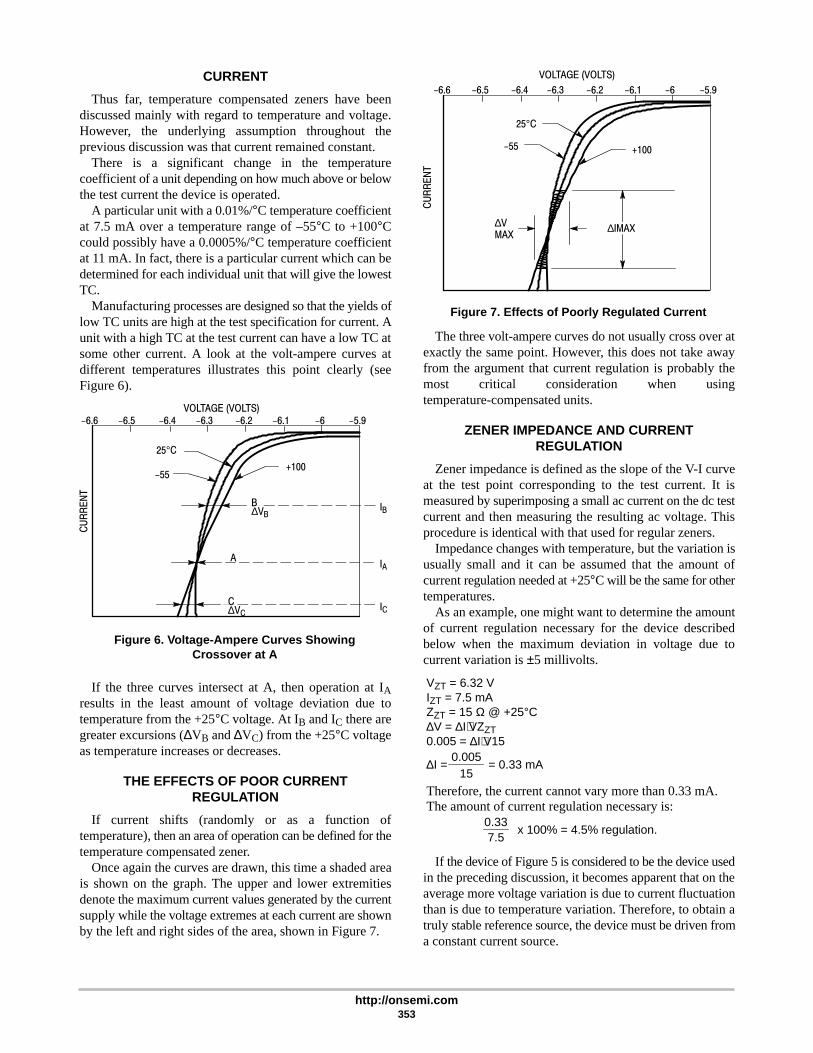
http://onsemi.com353
CURRENT
Thus far, temperature compensated zeners have beendiscussed mainly with regard to temperature and voltage.However, the underlying assumption throughout theprevious discussion was that current remained constant.
There is a significant change in the temperaturecoefficient of a unit depending on how much above or belowthe test current the device is operated.
A particular unit with a 0.01%/°C temperature coefficientat 7.5 mA over a temperature range of –55°C to +100°Ccould possibly have a 0.0005%/°C temperature coefficientat 11 mA. In fact, there is a particular current which can bedetermined for each individual unit that will give the lowestTC.
Manufacturing processes are designed so that the yields oflow TC units are high at the test specification for current. Aunit with a high TC at the test current can have a low TC atsome other current. A look at the volt-ampere curves atdifferent temperatures illustrates this point clearly (seeFigure 6).
VOLTAGE (VOLTS)-6.6 -6.5 -6.4 -6.3 -6.2 -6.1 -6 -5.9
IB
IA
IC
CU
RR
EN
T
25°C
-55+100
∆VB
B
A
C∆VC
Figure 6. Voltage-Ampere Curves ShowingCrossover at A
If the three curves intersect at A, then operation at IAresults in the least amount of voltage deviation due totemperature from the +25°C voltage. At IB and IC there aregreater excursions (∆VB and ∆VC) from the +25°C voltageas temperature increases or decreases.
THE EFFECTS OF POOR CURRENTREGULATION
If current shifts (randomly or as a function oftemperature), then an area of operation can be defined for thetemperature compensated zener.
Once again the curves are drawn, this time a shaded areais shown on the graph. The upper and lower extremitiesdenote the maximum current values generated by the currentsupply while the voltage extremes at each current are shownby the left and right sides of the area, shown in Figure 7.
VOLTAGE (VOLTS)
-6.6 -6.5 -6.4 -6.3 -6.2 -6.1 -6 -5.9
CU
RR
EN
T
25°C
-55 +100
∆IMAX∆VMAX
Figure 7. Effects of Poorly Regulated Current
The three volt-ampere curves do not usually cross over atexactly the same point. However, this does not take awayfrom the argument that current regulation is probably themost critical consideration when usingtemperature-compensated units.
ZENER IMPEDANCE AND CURRENTREGULATION
Zener impedance is defined as the slope of the V-I curveat the test point corresponding to the test current. It ismeasured by superimposing a small ac current on the dc testcurrent and then measuring the resulting ac voltage. Thisprocedure is identical with that used for regular zeners.
Impedance changes with temperature, but the variation isusually small and it can be assumed that the amount ofcurrent regulation needed at +25°C will be the same for othertemperatures.
As an example, one might want to determine the amountof current regulation necessary for the device describedbelow when the maximum deviation in voltage due tocurrent variation is ±5 millivolts.
VZT = 6.32 VIZT = 7.5 mAZZT = 15 Ω @ +25°C∆V = ∆I⋅VZZT0.005 = ∆I⋅V15
∆I =0.005
15= 0.33 mA
Therefore, the current cannot vary more than 0.33 mA.The amount of current regulation necessary is:
0.337.5
x 100% = 4.5% regulation.
If the device of Figure 5 is considered to be the device usedin the preceding discussion, it becomes apparent that on theaverage more voltage variation is due to current fluctuationthan is due to temperature variation. Therefore, to obtain atruly stable reference source, the device must be driven froma constant current source.

http://onsemi.com354
BASIC VOLTAGE REGULATION USING ZENER DIODES
BASIC CONCEPTS OF REGULATION
The purpose of any regulator circuit is to minimize outputvariations with respect to variations in input, temperature,and load requirements. The most obvious use of a regulatoris in the design of a power supply, but any circuit thatincorporates regulatory technique to give a controlledoutput or function can be considered as a regulator. Ingeneral, to provide a regulated output voltage, electroniccircuitry will be used to pass an output voltage that issignificantly lower than the input voltage and block allvoltage in excess of the desired output. Allocations shouldalso be made in the regulation circuitry to maintain thisoutput voltage for variation in load current demand.
There are some basic rules of thumb for the electricalrequirements of the electronic circuitry in order for it toprovide regulation. Number one, the output impedanceshould be kept as low as possible. Number two, a controllingreference needs to be established that is relativelyinsensitive to the prevailing variables. In order to illustratethe importance of these rules, an analysis of some simpleregulator circuits will point out the validity of thestatements. The circuit of Figure 1 can be considered aregulator. This circuit will serve to illustrate the importanceof a low output impedance.
The resistors RS and RR can be considered as the sourceand regulator impedances, respectively.
The output of the circuit is:
RS
RRRL
RR RL
(1)
VO = VI xRRRL
RR + RLRS +
RRRL
RR + RL=
VI
RS
RL
RS
RR+ + 1
Figure 1. Shunt Resistance Regulator
+
-
RS
RR RL
+
-
VI VO
For a given incremental change in VI, the changes in VOwill be:
(2)R RRRL
RR ∆VO = ∆VI
1
RS
RL
RS
RR+ + 1
Assuming RL fixed at some constant value, it is obviousfrom equation (2) that in order to minimize changes in VOfor variations in VI, the shunt resistor RR should be made assmall as possible with respect to the source resistor RS.Obviously, the better this relation becomes, the larger VI is
going to have to be for the same VO, and not until the ratioof RS to RR reaches infinity will the output be held entirelyconstant for variation in VI. This, of course, is animpossibility, but it does stress the fact that the regulationimproves as the output impedance becomes lower and lower.Where the output impedance of Figure 1 is given by
(3)RO =RSRR
RS + RR
It is apparent from this relation that as regulation isimproving with RS increasing and RR decreasing the outputimpedance RO is decreasing, and is approximately equal toRR as the ratio is 10 times or greater. The regulation of thiscircuit can be greatly improved by inserting a referencesource of voltage in series with RR such as Figure 2.
Figure 2. Regulator with Battery Reference Source
+
-
RS
VR
RL
RR
+
-
VI VO
The resistance RR represents the internal impedance of thebattery. For this circuit, the output is
(4)VO = VR + VIV
RS
RL
RS
RR+ + 1
Then for incremental changes in the input VI, the changesin VO will be dependent on the second term of equation(4), which again makes the regulation dependent on theratio of RS to RR. Where changes in the output voltageor the regulation of the circuit in Figure 1 were directlyand solely dependent upon the input voltage and outputimpedance, the regulation of circuit 2 will have an outputthat varies about the reference source VR in accordancewith the magnitude of battery resistance RR and itsfluctuations for changes in VI. Theoretically, if a perfectbattery were used, that is, VR is constant and RR is zero,the circuit would be a perfect regulator. In other words,in line with the basic rules of thumb the circuit exhibitsoptimum regulation with an output impedance of zero, anda constant reference source.
For regulator application, a zener diode can be usedinstead of a battery with a number of advantages. A battery’sresistance and nominal voltage will change with age andload demand; the ON Semiconductor zener diodecharacteristics remain unchanged when operating within its

http://onsemi.com355
specified limits. Any voltage value from a couple of volts tohundreds of volts is available with zener diodes, whereconventional batteries are limited in the nominal valuesavailable. Also, the zener presents a definite size advantage,and is less expensive than a battery because it is permanentand need not be regularly replaced. The basic zener diodeshunt regulator circuit is shown in Figure 3.
Figure 3. Basic Zener Diode Shunt Regulator
+
-
RS
RL
RZ
VZ
ZENER
DIODE
+
-
VI VO
Depending upon the operating conditions of the device, azener diode will exhibit some relatively low zenerimpedance RZ and have a specified breakover voltage of VZthat is essentially constant. These inherent characteristicsmake the zener diode suited for voltage regulatorapplications.
DESIGNING THE ZENER SHUNT REGULATOR
For any given application of a zener diode shunt regulator,it will be required to know the input voltage variations andoutput load requirements. The calculation of componentvalues will be directly dependent upon the circuitrequirements. The input may be constant or have maximumand minimum values depending upon the natural regulationor waveform of the supply source. The output voltage willbe determined by the designer’s choice of VZ and the circuitrequirements. The actual value of VZ will be dependentupon the manufacturer’s tolerance and some small variationfor different zener currents and operating temperatures.
For all practical purposes, the value of VZ as specified onthe manufacturer’s data sheet can be used to approximateVO in computing component values. The requirement forload current will be known and will vary within some givenrange of IL(min) to IL(max).
The design objective of Figure 3 is to determine the propervalues of the series resistance, RS, and zener powerdissipation, PZ. A general solution for these values can bedeveloped as follows, when the following conditions areknown:
VI (input voltage) from VI(min) to VI(max)
VO (output voltage) from VZ(min) to VZ(max)
IL (load current) from IL(min) to IL(max)
The value of RS must be of such a value so that the zenercurrent will not drop below a minimum value of IZ(min).This minimum zener current is mandatory to keep the
device in the breakover region in order to maintain thezener voltage reference. The minimum current can be eitherchosen at some point beyond the knee or found on themanufacturer’s data sheet (IZK). The basic voltage loopequation for this circuit is:
(5)VI = (IZ + IL)RS + VZ
The minimum zener current will occur when VI isminimum, VZ is maximum, and IL is maximum, thensolving for RS, we have:
(6)VI(min) – VZ(max)
IZ(min) + IL(max)RS =
Having found RS, we can determine the maximum powerdissipation PZ for the zener diode.
PZ(max) = VZ(max)VI(max) VZ(min)RS
IL(min)
(7)
(8)
(9)
PZ(max) = IZ(max) VZ(max)
Where:
IZ(max) =VI(max) – VZ(min)
RS– IL(min)
Therefore:
VI(max) – VZ(min)
RS– IL(min)
Once the basic regulator components values have beendetermined, adequate considerations will have to be given tothe variation in VO. The changes in VO are a function of fourdifferent factors; namely, changes in VI, IL, temperature, andthe value of zener impedance, RZ. These changes in VO canbe expressed as:
(10)RSRZ
RS + RZ
∆VI
RS
RZ
RS
RL+
1 +∆VO = – ∆IL + TC∆TVZ
The value of ∆VO as calculated with equation (10) willquite probably be slightly different from the actual valuewhen measured empirically. For all practical purposesthough, this difference will be insignificant for regulatordesigns utilizing the conventional commercial line of zenerdiodes.
Obviously to precisely predict ∆VO with a given zenerdiode, exact information would be needed about the zenerimpedance and temperature coefficient throughout thevariation of zener current. The “worst case” change can onlybe approximated by using maximum zener impedance andwith typical temperature coefficient.
The basic zener shunt regulator can be modified tominimize the effects of each term in the regulation equation(10). Taking one term at a time, it is apparent that theregulation or changes in output ∆VO will be improved if themagnitude of ∆VI is reduced. A practical and widely usedtechnique to reduce input variation is to cascade zener shuntregulators such as shown in Figure 4.

http://onsemi.com356
Figure 4. Cascaded Zener Shunt Regulators Reduce∆VO by Reducing ∆VI to the Succeeding Stages
-
+RS2
Z1 RL
RS1
-
Z2RL′
+
VI VOVO′ = VI′ = VZ1
This, in essence, is a regulator driven with a pre-regulatorso that the over all regulation is the product of both. Theregulation or changes in output voltage is determined by:
Where:
RL′ = RS2 +RLRZ2
RL + RZ2and IL′ = IL + IZ2
(11)
RS2RZ2
RS2 + RZ2
∆VZI
RS2
RL+1 +
∆VO = –
∆IL + TC2 ∆TVZ2
RS2
RZ2
(12)
RS1RZ1
RS1 + RZ1
∆VI
RS1
RL′ +1 +
∆VZ1 = ∆VO′ = –
∆IL′ + TC1 ∆TVZ1
RS1
RZ1
The changes in output with respect to changes in input forboth stages assuming the temperature and load are constantis
(13)∆VO∆VZ1
∆VO∆VO′= = Regulation of second stage
(14)
(15)
= Regulation of first stage
∆VO′∆VI
= Combined regulationx∆VO∆VO′=
∆VO∆VI
∆VO′∆VI
Obviously, this technique will vastly improve overallregulation where the input fluctuates over a relatively widerange. As an example, let’s say the input varies by ±20% andthe regulation of each individual stage reduces the variationby a factor of 1/20. This then gives an overall outputvariation of ±20% × (1/20)2 or ±0.05%.
The next two factors in equation (10) affecting regulationare changes in load current and temperature excursions. Inorder to minimize changes for load current variation, theoutput impedance RZRS/(RZ + RS) will have to be reduced.This can only be done by having a lower zener impedancebecause the value of RS is fixed by circuit requirements.There are basically two ways that a lower zener impedancecan be achieved. One, a higher wattage device can be usedwhich allows for an increase in zener current of which willreduce the impedance. The other technique is to series lowervoltage devices to obtain the desired equivalent voltage, sothat the sum of the impedance is less than that for a single
high voltage device. So to speak, this technique will kill twobirds with one stone, as it can also be used to minimizetemperature induced variations of the regulator.
In most regulator applications, the single most detrimentalfactor affecting regulation is that of variation in junctiontemperature. The junction temperature is a function of boththe ambient temperature and that of self heating. In order toillustrate how the overall temperature coefficient isimproved with series lower voltage zener, a mathematicalrelationship can be developed. Consider the diagram ofFigure 5.
Figure 5. Series Zener Improve Dynamic Impedanceand Temperature Coefficient
+
-
RS
RL
Z1
Z2
Zn
+
-
VI VO
With the temperature coefficient TC defined as the % changeper °C, the change in output for a given temperature rangewill equal some overall TC x ∆T x Total VZ. Such as
(16)∆VO(∆T) = TC ∆T (VZ1 + VZ2 + . . . + VZN)
Obviously, the change in output will also be equal to thesum of the changes as attributed from each zener.
(17)∆VO(∆T) = ∆T(TC1VZ1 + TC2VZ2 + . . . + TCNVZN)
Setting the two equations equal to each other and solvingfor the overall TC, we get
(18)
(19)
TC∆T(VZ1 + VZ2 + . . . + VZN) = ∆T(TC1VZ1+ TC2VZ2 + . . . + TCNVZN)
TC =TC1 VZ1 + TC2VZ2 + . . . + TCNVZN
VZ1 + VZ2 + . . . + VZN
For equation (19) the overall temperature coefficient forany combination of series zeners can be calculated. Say forinstance several identical zeners in series replace a singlehigher voltage zener. The new overall temperaturecoefficient will now be that of one of the low voltagedevices. This allows the designer to go to the manufacturer’s

http://onsemi.com357
data sheet and select a combination of low TC zener diodesin place of the single higher TC devices. Generally speaking,the technique of using multiple devices will also yield alower dynamic impedance. Advantages of this technique arebest demonstrated by example. Consider a 5 watt diode witha nominal zener voltage of 10 volts exhibits approximately0.055% change in voltage per degree centrigrade, a 20 voltunit approximately 0.075%/°C, and a 100 volt unitapproximately 0.1%/°C. In the case of the 100 volt diode,five 20 volt diodes could be connected together to providethe correct voltage reference, but the overall temperaturecoefficient would remain that of the low voltage units, i.e.0.075%/°C. It should also be noted that the same seriescombination improves the overall zener impedance inaddition to the temperature coefficient. A 20 volt, 5 wattON Semiconductor zener diode has a maximum zenerimpedance of 3 ohms, compared to the 90 ohms impedancewhich is maximum for a 100 volt unit. Although theseimpedances are measured at different current levels, theseries impedance of five 20 volt zener diodes is still muchlower than that of a single 100 volt zener diode at the testcurrent specified on the data sheet.
For the ultimate in zener shunt regulator performance, theaforementioned techniques can be combined with the properselection of devices to yield an overall improvement inregulation. For instance, a multiple string of low voltagezener diodes can be used as a preregulator, with a seriescombination of zero TC reference diodes in the final stagesuch as Figure 6.
The first stage will reduce the large variation in VI to somerelatively low level, i.e. ∆VZ. This ∆VZ is optimized byutilizing a series combination of zeners to reduce the overallTC and ∆VZ. Because of this small fluctuation of input to thesecond stage, and if RL is constant, the biasing current of theTC units can be maintained at their specified level. This willgive an output that is very precise and not significantlyaffected by changes in input voltage or junction temperature.
Figure 6. Series Zeners Cascaded With SeriesReference Diodes for Improved Zener
Shunt Regulation
RS1 RS2
Z1
Z2
Z3
Z4
RL
TC1
TC2
+
-
+
-
VI VO
The basic zener shunt regulator exhibits some inherentlimitations to the designer. First of all, the zener is limited toits particular power dissipating rating which may be lessthan the required amount for a particular situation. The totalmagnitude of dissipation can be increased to some degree byutilizing series or parallel units. Zeners in series present few
problems because individual voltages are additive and thedevices all carry the same current and the extent that thistechnique can be used is only restricted by the feasibility ofcircuit parameters and cost. On the other hand, caution mustbe taken when attempting to parallel zener diodes. If thedevices are not closely matched so that they all break overat the same voltage, the low voltage device will go intoconduction first and ultimately carry all the current. In orderto avoid this situation, the diodes should be matched forequal current sharing.
EXTENDING POWER AND CURRENT RANGE
The most common practice for extending the powerhandling capabilities of a regulator is to incorporatetransistors in the design. This technique is discussed in detailin the following sections of this chapter. The seconddisadvantage to the basic zener shunt regulator is thatbecause the device does not have a gain function, a feedbacksystem is not possible with just the zener resistorcombination. For very precise regulators, the design willnormally be an electronic circuit consisting of transistordevices for control, probably a closed loop feedback systemwith a zener device as the basic referencing element.
The concept of regulation can be further extended andimproved with the addition of transistors as the powerabsorbing elements to the zener diodes establishing areference. There are three basic techniques used thatcombine zener diodes and transistors for voltage regulation.The shunt transistor type shown in Figure 7 will extend thepower handling capabilities of the basic shunt regulator, andexhibit marked improvement in regulation.
Figure 7. Basic Transistor Shunt Regulator
RL
RS
ZIZIC
RB
IB
VBE
Q1IL
-
+
-
+
VI VO
In this configuration the source resistance must be largeenough to absorb the overvoltage in the same manner as inthe conventional zener shunt regulator. Most of the shuntregulating current in this circuit will pass through thetransistor reducing the current requirements of the zenerdiode by essentially the dc current gain of the transistor hFE.Where the total regulating shunt current is:
(20)
IS = IZ + IC = IZ + IB hFE
where
therefore
IZ = IB + IRB and IB >> IRB
IS ≈ IZ + IZ hFE = IZ (1 + hFE)

http://onsemi.com358
The output voltage is the reference voltage VZ plus theforward junction drop from base to emitter VBE of thetransistor.
(21)VO = VZ + VBE
The values of components and their operating conditionis dictated by the specific input and output requirements andthe characteristics of the designer’s chosen devices, asshown in the following relations:
(22)RS =VI(min) – VO(max)
IZ(min) [1+hFE(min)] + IL(max)
RB =VI(min) – VZ(max)
IZ(min)
PDZ = IZ(max) VZ(max)
when
IZ(max) =VI(max) V O(min)
RS IL(min) 1
1 hFE(min)
hence
VI(max) – VO(min)
RS– IL(min)
11 + hFE(min)
PDZ =VI(max) VO(min)
RS IL(min) 1
1 hFE(min)VI(max) – VO(min)
RS– IL(min)
VZ(max)
1 + hFE(min)
PDQ =VI(max) V O(min)
RS IL(min) 1888888VI(max) – VO(min)
RS– IL(min) VO(max)
(23)
(24)
(25)
(26)
(27)
Regulation with this circuit is derived in essentially thesame manner as in the shunt zener circuit, where the outputimpedance is low and the output voltage is a function of thereference voltage. The regulation is improved with thisconfiguration because the small signal output impedance isreduced by the gain of Q1 by 1/hFE.
One other highly desirable feature of this type of regulatoris that the output is somewhat self compensating fortemperature changes by the opposing changes in VZ andVBE for VZ ≈ 10 volts. With the zener having a positive2 mV/°C TC and the transistor base to emitter being anegative 2 mV/°C TC, therefore, a change in one is cancelledby the change in the other. Even though this circuit is a veryeffective regulator it is somewhat undesirable from anefficiency standpoint. Because the magnitude of RS isrequired to be large, and it must carry the entire inputcurrent, a large percentage of power is lost from input tooutput.
EMITTER FOLLOWER REGULATOR
Another basic technique of transistor-zener regulation isthat of the emitter follower type shown in Figure 8.
Figure 8. Emitter Follower Regulator
RS
RB
Z1
IRB
IZ
+
-VBE
-
+
IL
RL
Q1IC
+
-
+
-
VI VO
This circuit has the desirable feature of using a seriestransistor to absorb overvoltages instead of a large fixedresistor, thereby giving a significant improvement inefficiency over the shunt type regulator. The transistor mustbe capable of carrying the entire load current andwithstanding voltages equal to the input voltage minus theload voltage. This, of course, imposes a much more stringentpower handling requirement upon the transistor than wasrequired in the shunt regulator. The output voltage is afunction of the zener reference voltage and the base toemitter drop of Q1 as expressed by the equation (28).
(28)VO = VZ – VBE
The load current is approximately equal to the transistorcollector current, such as shown in equation (29).
(29)IL(max) ≈ IC(max)
The designer must select a transistor that will meet thefollowing basic requirements:
(30)
PD ≅ (VI(max) – VO)IL(max)
IC(max) ≈ IL(max)
BVCES ≥ (VI(max) – VO)
Depending upon the designer’s choice of a transistor andthe imposed circuit requirements, the operation conditionsof the circuit are expressed by the following equations:
(31)
VZ = VO + VBE
= VO + IL(max)/gFE(min) @ IL(max)
RS =VI(min) – VZ – VCE(min) @ IL(max)
IL(max)
Where VCE(min) is an arbitrary value of minimumcollector to emitter voltage and gFE is the transconductance.
This is sufficient to keep the transistor out of saturation,which is usually about 2 volts.

http://onsemi.com359
(32)RB =
VCE(min) @ IL(max)
IL(max)/hFE(min) @ IL(max) + IZ(min)
IZ(max) =VI(max) –VZ
RB + RZ
PDZ = IZ(max)VZ
Actual PDQ = (VI(max) – VO) IL(max)
(33)
(34)
(35)
There are two primary factors that effect the regulationmost in a circuit of this type. First of all, the zener currentmay vary over a considerable range as the input changesfrom minimum to maximum and this, of course, may havea significant effect on the value of VZ and therefore VO.Secondly, VZ and VBE will both be effected by temperaturechanges which are additive on their effect of output voltage.This can be seen by altering equation (28) to show changesin VO as dependent on temperature, see equation (36).
(36)VO(∆T) = ∆T[(+TC) VZ – (–TC) VBE]
The effects of these detrimental factors can be minimizedby replacing the bleeder resistor RB with a constant currentsource and the zener with a reference diode in series with aforward biased diode (see Figure 9).
Figure 9. Improved Emitter Follower Regulator
+
-
+
-RS
RL
Q1
FORWARDBIAS DIODE
TC ZENER
IB = K
CONSTANT
CURRENT
SOURCE
VI VO
The constant current source can be either a current limiterdiode or a transistor source. The current limiter diode isideally suited for applications of this type, because it willsupply the same biasing current irregardless of collector tobase voltage swing as long as it is within the voltage limitsof the device. This technique will overcome changes in VZfor changes in IZ and temperature, but changes in VBE dueto load current changes are still directly reflected upon theoutput. This can be reduced somewhat by combining a
transistor with the zener for the shunt control element asillustrated in Figure 10.
Figure 10. Series Pass Regulator
+
-
RL
Z1
Q2
Q1
RB
RS
IC2
CONSTANT
CURRENT
SOURCE
VI VO
This is the third basic technique used for transistor-zenerregulators. This technique or at least a variation of it, findsthe widest use in practical applications. In this circuit thetransistor Q1 is still the series control device operating as anemitter follower. The output voltage is now established bythe transistor Q2 base to emitter voltage and the zenervoltage. Because the zener is only supplying base drive toQ2, and it derives its bias from the output, the zener currentremains essential constant, which minimizes changes in VZdue to IZ excursions. Also, it may be possible (VZ ≈ 10 V)to match the zener to the base-emitter junction of Q2 for anoutput that is insensitive to temperature changes. Theconstant current source looks like a very high loadimpedance to the collector of Q2 thus assuming a very highvoltage gain. There are three primary advantages gainedwith this configuration over the basic emitter follower:
1. The increased voltage gain of the circuit with theaddition of Q2 will improve regulation for changes inboth load and input.
2. The zener current excursions are reduced, therebyimproving regulation.
3. For certain voltages the configuration allows goodtemperature compensation by matching thetemperature characteristics of the zener to thebase-emitter junction of Q2.
The series pass regulator is superior to the other transistorregulators thus far discussed. It has good efficiency, betterstability and regulation, and is simple enough to beeconomically practical for a large percentage ofapplications.

http://onsemi.com360
Figure 11. Block Diagram of Regulator with Feedback
REGULATING
POWER
ELEMENT
CONTROL
UNITAMPLIFIER
REFERENCE
AND
ERROR
DETECTION
LOADINPUT OUTPUT
EMPLOYING FEEDBACK FOROPTIMUM REGULATION
The regulators discussed thus far do not employ anyfeedback techniques for precise control and compensationand, therefore, find limited use where an ultra preciseregulator is required. In the more sophisticated regulatorssome form of error detection is incorporated and amplifiedthrough a feedback network to closely control the powerelements as illustrated in the block diagram of Figure 11.
Regulating circuits of this type will vary in complexityand configuration from application to application. Thistechnique can best be illustrated with a couple of actualcircuits of this type. The feedback regulators will generallybe some form of series pass regulator, for optimumperformance and efficiency. A practical circuit of this typethat is extensively utilized is shown in Figure 12.
In this circuit, the zener establishes a reference level forthe differential amplifier composed of Q4 and Q5 which willset the base drive for the control transistor Q3 to regulate theseries high gain transistor combination of Q1 and Q2. Thedifferential amplifier samples the output at the voltagedividing network of R8, R9, and R10. This is compared to thereference voltage provided by the zener Z1. The difference,if any, is amplified and fed back to the control elements. Byadjusting the potentiometer, R9, the output level can be setto any desired value within the range of the supply. (Theoutput voltage is set by the relation VO = VZ[(RX +RY)/RX].) By matching the transistor Q4 and Q5 forvariations in VBE and gain with temperature changes andincorporating a temperature compensated diode as thereference, the circuit will be ultra stable to temperatureeffects. The regulation and stability of this circuit is verygood, and for this reason is used in a large percentage ofcommercial power supplies.
Figure 12. Series Pass Regulator with Error Detection and FeedbackAmplification Derived from a Differential Amplifier
R1
R4
Q2Q4
Q3 C1
Q1
R2
R3
Q5
RL
Z1
R5 R6
R7
R9
R10
+
- -
R8RX
RY
+
VI VO

http://onsemi.com361
Figure 13. Series Pass Regulator with Temperature Compensated Reference Amplifier
+
-
+
-
R1
R2RL
R3
R5
R4
R8
R6
R7
D1
Q1
Q2
Q3
REFERENCE
AMPLIFIER
VI VO
Another variation of the feedback series pass regulator isshown in Figure 13. This circuit incorporates a stabletemperature compensated reference amplifier as the primarycontrol element.
This circuit also employs error detection and amplifiedfeedback compensation. It is an improved version over thebasic series pass regulator shown in Figure 10. The serieselement is composed of a Darlington high gainconfiguration formed by Q1 and Q2 for an improvedregulation factor. The combined gain of the referenceamplifier and Q3 is incorporated to control the series unit.This reduced the required collector current change of thereference amplifier to control the regulator so that the biascurrent remains close to the specified current for lowtemperature coefficient. Also the germanium diode D1 willcompensate for the base to emitter change in Q3 and keep thereference amplifier collector biasing current fairly constantwith temperature changes. Proper biasing of the zener andtransistor in the reference amplifier must be adhered to if theoutput voltage changes are to be minimized.
CONSTANT CURRENT SOURCES FORREGULATOR APPLICATIONS
Several places throughout this chapter emphasize theneed for maintaining a constant current level in the variousbiasing circuits for optimum regulation. As was mentionedpreviously in the discussion on the basic series passregulator, the current limiter diode can be effectively usedfor the purpose.
Aside from the current limiter diode a transistorizedsource can be used. A widely used technique is shownincorporated in a basic series pass regulator in Figure 14.
The circuit is used as a preregulated current source tosupply the biasing current to the transistor Q2. The constantcurrent circuit is seldom used alone, but does find wide usein conjunction with voltage regulators to supply biasingcurrent to transistors or reference diodes for stableoperation. The Zener Z2 establishes a fixed voltage acrossRE and the base to emitter of Q3. This gives an emittercurrent of IE = (VZ – VBE)/RE which will vary only slightlyfor changes in input voltage and temperature.
Figure 14. Constant Current Source Incorporated in a Basic Regulator Circuit
Q1
Q2
Q3
RB1
Z1
RL
REZ2
RB2
CONSTANT
CURRENT
SOURCE
--
++
VI VO

http://onsemi.com362
IMPEDANCE CANCELLATION
One of the most common applications of zener diodes isin the general category of reference voltage supplies. Thefunction of the zener diode in such applications is to providea stable reference voltage during input voltage variations.This function is complicated by the zener diode impedance,which effectively causes an incremental change in zenerbreakdown voltage with changing zener current.
Figure 15. Impedance Cancellation with AnUncompensated Zener
R2R1
Z1 TC1
+
-
VI
It is possible, however, by employing a bridge type circuitwhich includes the zener diode and current regulatingresistance in its branch legs, to effectively cancel the effectof the zener impedance. Consider the circuit of Figure 15 asan example. This is the common configuration for a zenerdiode voltage regulating system. The zener impedance at 20mA of a 1N4740 diode is typically 2 ohms. If the supplyvoltage now changes from 30 V to 40 V, the diode currentdetermined by R1 changes from 20 to 30 mA; the averagezener impedance becomes 1.9 ohms; and the referencevoltage shifts by 19 mV. This represents a reference changeof .19%, an amount far too large for an input change of 30%in most reference supplies.
The effect of zener impedance change with current isrelatively small for most input changes and will be neglectedfor this analysis. Assuming constant zener impedance, thezener voltage is approximated by
(37)V′Z = VZ + Z(I′Z – IZ)
where V′Z is the new zener voltageVZ is the former zener voltageI′Z is the new zener currentIZ is the new zener current flowing at VZRZ is the zener impedance
Then
Let the input voltage VI in Figure 15 increase by anamount ∆VI
Then ∆I =∆VI – ∆VZ
R1
∆VZ
RZAlso ∆I =
Solving ∆VIRZ – ∆VZRZ – ∆VZR1 = 0
∆VZ
∆VIOr =
RZ
R1 + RZ
(39)
(38)
(40)
∆VZ = Z∆IZ
Equation 40 merely states that the change in referencevoltage with input tends to zero when the zener impedancetends also to zero, as expected.
The figure of merit equation can be applied to the circuitsof Figure 16 and 17 to explain impedance cancellation. TheChange Factor equations for each leg and the referencevoltage VR are:
(41)
(43)
(42)
CFVZ =∆VZ
∆VI
RZ
R1 + RZ= = RA
R3
R2 + R3
∆V2
∆VICFV2 = = = RB
RZ
R1 + RZ
∆VR
∆VICFVR = = = RA – RB
R3
R2 + R3=
Figure 16. Standard VoltageRegulation Circuit
R1
VI′ ∆VI
I
VZ
Figure 17. Impedance Cancellation Bridge
VI′ ∆VI
R3
R1R2
VR
V2VZ

http://onsemi.com363
Since the design is to minimize CFVR, RB can be set equalto RA. The Input Regulation Factors are:
(44)
(46)
(45)
γVZ =∆VZ
∆VI VI
ViZ =
1VI
VZ1 +
VZ
VI VI
ViZR1
RZ
γV2 =∆V2
∆VI VI
ViZ = 1
VI
V2
γVR =∆VR
∆VI VI
ViZ =
1VI
VR1 + VI
ViZR1
RZ VI
ViZVZ
VI VI
Vi Z1
1 –RB
RA
It is seen that γVR can be minimized by setting RB = RA.Note that it is not necessary to match R3 to RZ and R2 to
R1. Thus R3 and R2 can be large and hence dissipate lowpower. This discussion is assuming very light load currents.

http://onsemi.com364
ZENER PROTECTIVE CIRCUITS AND TECHNIQUES:BASIC DESIGN CONSIDERATIONS
INTRODUCTION
The reliability of any system is a function of the ability ofthe equipment to operate satisfactorily during moderatechanges of environment, and to protect itself duringotherwise damaging catastrophic changes. The silicon zenerdiode offers a convenient, simple but effective means ofachieving this result. Its precise voltage sensitivebreakdown characteristic provides an accurate limitingelement in the protective circuit. The extremely highswitching speed possible with the zener phenomenon allowsthe circuit to react faster by orders of magnitude thatcomparable mechanical and magnetic systems.
By shunting a component, circuit, or system with a zenerdiode, the applied voltage cannot exceed that of theparticular device’s breakdown voltage. (See Figure 1.)
A device should be chosen so that its zener voltage issomewhat higher than the nominal operating voltage butlower than the value of voltage that would be damaging ifallowed to pass. In order to adequately incorporate the zenerdiode for circuit protection, the designer must considerseveral factors in addition to the required zener voltage. Thefirst thing the designer should know is just what transientcharacteristics can be anticipated, such as magnitude,duration, and the rate of reoccurrence. For short durationtransients, it is usually possible to suppress the voltage spikeand allow the zener to shunt the transient current away fromthe load without a circuit shutdown. On the other hand, if theover-voltage condition is for a long duration, the protectivecircuit may need to be complimented with a disconnectelement to protect the zener from damage created byexcessive heating. In all cases, the end circuit will have to bedesigned around the junction temperature limits of thedevice.
The following sections illustrate the most common zenerprotective circuits, and will demonstrate the criteria to befollowed for an adequate design.
BASIC PROTECTIVE CIRCUITSFOR SUPPLY TRANSIENTS
The simple zener shunt protection circuit shown inFigure 1 is widely used for supply voltage transientprotection where the duration is relatively short. The circuitapplies whether the load is an individual component or acomplete circuit requiring protection. Whenever the inputexceeds the zener voltage, the device avalanches intoconduction clamping the load voltage to VZ. The totalcurrent the diode must carry is determined by the magnitude
of the input voltage transient and the total circuit impedanceminus the load current. The worst case occurs when loadcurrent is zero and may be expressed as follows:
IZ(max) =VI(max) – VZ
RS(1)
Figure 1. Basic Shunt Zener TransientProtection Circuit
LOADZPOWER
SUPPLY
RS+
-
The maximum power dissipated by the zener is
PZ(max) = IZ(max) VZ(max)=VI(max) – VZ
RS(2)VZ(max)
Also, more than one device can be used, i.e., a seriesstring, which will reduce the percentage of total power to bedissipated per device by a factor equal to the number ofdevices in series. The number of diodes required can befound from the following expression:
Number =PZ(max)
PZ (allowable per device)(3)
Any fraction of a zener must be taken as the next highestwhole number. This design discussion has been based uponthe assumption that the transient is of a single shot,non-recurrent type. For all practical purposes it can beconsidered non-recurrent if the “off period” betweentransients is at least four times the thermal time constant ofthe device. If the “off period” is shorter than this, then thedesign calculations must include a factor for the duty cycle.This is discussed in detail in Chapter 4. In Chapter 4 there arealso some typical curves relating peak power, pulse durationand duty cycle that may be appropriate for some designs.
Obviously, the factor that limits the feasibility of the basiczener shunt protective circuit is the pulse durations “t”. Asthe duration increases, the allowable peak power for a givenconfiguration decreases and will approach a steady statecondition.

http://onsemi.com365
Figure 2. Overvoltage Protection with Zener Diodes and Fuses
LOAD
R CVS
RS FUSE
POWERSUPPLY
+
-
When the anticipated transients expected to prevail for aspecific situation are of long duration, a basic zener shuntbecomes impractical, in such a case the circuit can beimproved by using a complementary disconnect element.The most common overload protective element is without adoubt the standard fuse. The common fuse adequatelyprotects circuit components from over-voltage surges, but atthe same time must be chosen to eliminate “nuisance fusing”which results when the maximum current rating of the fuseis too close to the normal operational current of the circuit.
AN EXAMPLE PROBLEM: SELECTING AFUSE-ZENER COMBINATION
Consider the case illustrated in Figure 2. Here the loadcomponents are represented by a parallel combination of Rand C, equivalent to many loads found in practice. Themaximum capacitor voltage rating is usually thecircuit-voltage limiting factor due to the cost of high voltagecapacitors. Consequently, a protective circuit must bedesigned to prevent voltage surges greater than 1.5 timesnormal working voltage of the capacitor. It is common,however, for the supply voltage to increase to 135% normalfor long periods. Examination of fuse manufacturers’melting time-current curves shows the difficulty of trying toselect a fuse which will melt rapidly at overload (within oneor two cycles of the supply frequency to prevent capacitordamage), and will not melt when subjected to voltages closeto overload for prolonged periods.
By connecting a zener diode of correct voltage ratingsacross the load as shown, a fuse large enough to withstandnormal current increases for long periods may be chosen.The sudden current increase when zener breakdown occursmelts the fuse rapidly and protects the load from largesurges. In Figure 3, fuse current was plotted against supplyvoltage to illustrate the improvement in load protectionobtained with zener-fuse combinations. Fuse current “A”would be selected to limit current resulting from voltagesurges above 112 V to 90 mA, which would melt the fuse in100 ms. It is a simple matter, however, to select a fuse whichmelts in 30 ms at 200 mA but is unaffected by 100 mAcurrents. The zener connection allows fuse current “B” to beselected, eliminating this design problem and providing afaster, more reliable protective circuit. If the same fuse wasused without the zener diode, a supply voltage of 210 volts
would be reached before the fuse would begin to protect theload.
VS, SUPPLY VOLTAGE (VOLTS)
60 70 80 90 100 110 120 130 14060
80
100
120
140
160
180
200
220
A"
B"
FU
SE
CU
RR
EN
T (m
A)
Figure 3. Fuse Current versusSupply Voltage
RESISTIVELOAD ONLY
ZENER DIODE WITH,RESISTIVE LOAD
ZENER BREAKDOWN,
VOLTAGENORMAL LOAD VOLTAGE
Selection of the correct power rating of zener diodes to beused for surge protection depends upon the magnitude andduration of anticipated surges. Often in circuits employingboth fuses and zener diodes, the limiting surge duration willbe the melting time of the fuse. This, in turn, depends on thenature of the load protected and the length of time it willtolerate an overload.
As a first solution to the example problem, consider azener diode with a nominal breakdown voltage of 110 voltsmeasured at a test current (IZT) of 110 mA. Since the fuserequires about 200 mA to melt and 100 mA are drawnthrough the load at this voltage, the load voltage will neverexceed the zener breakdown voltage on slowly rising inputs.Transients producing currents of approximately 200 mA butof shorter duration than 30 ms will simply be clipped byzener action and diverted from the load. Transients of veryhigh voltage will produce larger currents and, hence, willmelt the fuse more rapidly. In the limiting case wheretransient power might eventually destroy the zener diode,the fuse always melts first because of the slower thermaltime constant inherent in the zener diode’s larger geometry.
The curves in Figure 4 illustrate the change in zenervoltage as a function of changing current for a typical devicetype.

http://onsemi.com366
LOG IZ/IZK
CH
AN
GE
, IN
VZ
VZ = V1
V2
V3
Figure 4. Change in V Z for Changes in I Z
If an actual curve for the device being used is notavailable, the zener voltage at a specific current above orbelow the test current may be approximated by equation 4.
Where: V = VZ + ZZT (I–IZT)VZ = zener voltage at test current IZTZZT = zener impedance at test current IZTIZT = test currentV = zener voltage at current I
(4)
For a given design, the maximum zener voltage to expectfor the higher zener current should be determined to makesure the limits of the circuit are met. If the maximum limitis excessive for the original device selection, the next lowervoltage rating should be used.
The previous discussion on design consideration forprotective circuits incorporating fuses is applicable to anyprotective element that permanently disconnects the supplywhen actuated. Rather than a fuse, a non-resetting magneticcircuit breaker could have been used, and the samereasoning would have applied.
LOAD CURRENT SURGES
In many actual problems the designer must choose aprotective circuit to perform still another task. Not only mustthe equipment be protected from the voltage surges in thesupply, but the supply itself often requires protection fromshorts or partial shorts in the load. A direct short in the loadis fairly easy to handle, as the drastic current change permitsthe use of fuses with ratings high enough to avoid problemswith supply surges. More common is the partial short, as
illustrated in Figure 5. If a short circuit occurs in thecapacitive section of the load (represented by C) theresulting fault current is limited by the resistive section(represented by R) to a value which may not be great enoughto melt the fuse. The fault current could be sufficient,however, to damage the supply and other components in theload.
The problem is resolved by employing a zener diode toprotect against supply surges as described in the previoussection, and by selecting a separate fuse to protect from loadfaults. The load fuse in Figure 5 is chosen close to the normaloperating current. Abnormal supply surges do not affect itand equipment operates reliably but with ample protectionfor the supply against load changes.
ZENER DIODES AND RECLOSINGDISCONNECT ELEMENTS
An interesting application of zener diodes as overvoltageprotectors, which offers the possibility of designing for bothlong and short duration surges, is shown in Figure 6.
Figure 6. Zener Diode Reclosing Circuit BreakerProtective Circuit
R
IZ
LOAD
POWER
SUPPLY
RECLOSING
CIRCUIT
BREAKER
In the event of a voltage overload exceeding a chosenzener voltage, a large current will be drawn through thediode. The reclosing disconnect element opens after aninterval determined by its time constant, and the supply isdisconnected. After another interval, again depending on theswitch characteristics, the supply is reconnected and thevoltage “sampled” by the zener diode. This leads to an“on-off” action which continues until the supply voltagedrops below the predetermined limit. At no time can the loadvoltage or current exceed that set by the zener. The chiefadvantage in this type of circuit is the elimination of fusereplacement in similar fusing circuits, while providingessentially the same load protection.
Figure 5. Supply and Load with Zener Diode; Fuse Circuitry
POWERSUPPLY
RSUPPLYFUSE
LOADFUSE R
C
LOAD

http://onsemi.com367
Figure 7. (Typical) Voltage, Current and Temperature Waveformsfor a Thermal Breaker
TIME
TIME
TIME
TIME
VOLTS
SUPPLY
VOLTAGE
°C
THERMAL
BREAKER
TEMPERATURE
AMPS
ZENER
DIODE
CURRENT
ZENER
DIODE
JUNCTION
TEMPERATURE
SURGE VOLTAGE
OVER VOLTAGE
NORMAL OPERATING VOLTAGE
BREAK TEMPERATURE
MAKE
TEMPERATURE
MAXIMUM TJ°C
It is difficult to define a set design procedure in this case,because of the wide variety of reclosing, magnetic andthermal circuit breakers available. Care should be taken toensure that the power dissipated in the zener diode during theconduction time of the disconnect element does not exceedits rating. As an example, assume the disconnect elementwas a thermal breaker switch. The waveforms for a typicalover-voltage situation are shown in Figure 7.
It is apparent that the highest zener diode junctiontemperature is reached during the first conduction period. Atthis time the thermal breaker is cold and requires the greatesttime to reach its break temperature. The breaker then cyclesthermally between the make and break temperatures as longas the supply voltage is greater than the zener voltage, asshown in Figure 7.
The zener diode current and junction temperaturevariation are shown in the last two waveforms of Figure 7.Overvoltage durations longer than the trip time of thethermal breaker do not affect the diode as the supply isdisconnected. An overvoltage of much higher level simply
causes the thermal breaker to open sooner. In effect, thezener diode rating must be high enough to ensure thatmaximum junction temperature is not reached during thelongest interval that the thermal switch will be closed.
Manufacturers of thermally operated circuit breakerspublish current-time curves for their devices similar to thatshown in Figure 8. By estimating the peak supplyovervoltage and determining the maximum overvoltagetolerated by the load, an estimation of peak zener current canbe made. The maximum breaker trip time may then be readfrom Figure 8. (After the initial current surge, the durationof “of” time is determined entirely by the breakercharacteristics and will vary widely with manufacture.) Thezener diode junction temperature rise during conductionmay be calculated now from the thermal time constant of thedevice and the heatsink used.
Because the reclosing circuit breaker is continuallycycling on and off, the zener current takes on thecharacteristics of a repetitive surge, as can be seen inFigure 7.

http://onsemi.com368
30
20
10
00 1 2 3
CURRENT (AMPS)
TR
IP T
IME
(S
EC
ON
DS
)
Figure 8. Trip Time versus Current forThermal Breaker
TRANSISTOR OVERVOLTAGE PROTECTION
In many electronic circuits employing transistors, highinternal voltages can be developed and, if applied to thetransistors, will destroy them. This situation is quitecommon in transistor circuits that are switching highlyinductive loads. A prime example of this would be intransistorized electronic ignition systems such as shown inFigures 9a and 9b.
The zener diode is an important component to assure solidstate ignition system reliability. There are two basic methods
of using a zener diode to protect an ignition transistor. Theseare shown in Figures 9a and 9b. In Figure 9b the transistoris protected by a zener diode connected between base andcollector and in Figure 9a, the zener is connected betweenemitter and collector. In both cases the voltage level of thezener must be selected carefully so that the voltage stress onthe transistor is in a region where the safe operating area isadequate for reliable circuit operation.
Figure 10 illustrates “safe” and “unsafe” selection of azener diode for collector-base protection of a transistor in theignition coil circuit. It can be seen that the safe operating areaof a transistor must be known if an adequate protective zeneris to be selected.
The zener diode must be able to take the stress of peakpulse current necessary to clamp the voltage rise across thetransistor to a safe value. In a typical case, a 5 watt, 100 voltzener transient suppressor diode is required to operate withan 80 µs peak pulse current of 8 amperes when connectedbetween the collector-emitter of the transistor. Thewaveform of this pulse current approaches a sine wave inshape (Figure 11). The voltage rise across a typical transientsuppressor diode due to this current pulse is shown in Figure12. This voltage rise of approximately 8 volts indicates aneffective zener impedance of approximately 1 ohm.However, a good share of this voltage rise is due to thetemperature coefficient and thermal time constant of thezener. The temperature rise of the zener diode junction isindicated by the voltage difference between the rise and fallof the current pulse.
Figure 9. Transistor Ignition Systems with ZenerOvervoltage Surge Protection
10 Ω1/2 W
1 Ω
10 Ω10 W
1 Ω100 W
560 pF
2 µF
5 Ω
1N5374B
1N6295
10 Ω
2N5879
+12 V
H.V. TODIST.
PRESTOLITE
201
MALLORY
COIL
28100
H.V. TO
DIST.
200 VPAPER
2N6031
+12 V
(A) (B)

http://onsemi.com369
COLLECTORBASE
ZENER CLAMP
10
0
9
8
7
6
5
4
3
2
1
0
SAFE
UNSAFE
IC
10 30 40 50 60 70 80 90 100 110 120
VCE
COLLECTOR
EMITTER
ZENER
CLAMP
TYPICAL TRANSISTOR SAFE AREA LIMIT
Figure 10. Safe Zener Protection
20
LOADLINE
SAFE
TIME 10 µs/div
2 A
/div
ZE
NE
R C
UR
RE
NT
Figure 11. Zener Diode Current Pulse
100 VZENER VOLTAGE 1 V/div
1 A
/div
ZE
NE
R C
UR
RE
NT
0
Figure 12. Voltage-Current Representation on100 V Zener
In order to assure safe operation, the change in zenerjunction temperature for the peak pulse conditions must beanalyzed. In making the calculation, the method describedin Chapter 3 should be used, taking into account duty cycle,pulse duration, and pulse magnitude.
When the zener diode is connected between the collectorand emitter of the transistor, additional power dissipationwill result from the clipping of the ringing voltage of theignition coil by the forward conduction of the zener diode.This power dissipation by the forward diode current will
result in additional zener voltage rise. It is not uncommon toobserve a 15-volt rise above the zener device voltage ratingdue to temperature coefficient and impedance under thesepulse current conditions.
The zener diode should be connected as close as possibleto the terminals of the transistor the zener is intended toprotect. This insures that induced voltage transients, causedby current changes in long lead lengths, are clamped by thezener and do not appear across the transistor.

http://onsemi.com370
Figure 13. DC-DC Converter with Surge Protecting Diodes
+
Another example of overvoltage protection of transistoroperating in an inductive load switch capacity is illustratedin Figure 13. The DC-DC converter circuit shows aconnection from collector to emitter of two zener diodes ascollector overvoltage protectors. Without some type oflimiting device, large voltage spikes may appear at thecollectors, due to the switching transients produced withnormal circuit operation. When this spike exceeds thecollector breakdown rating of the transistor, transistor life isconsiderably shortened. The zener diodes shown are chosenwith zener breakdowns slightly below transistor breakdownvoltage to provide the necessary clipping action. Since thespikes are normally of short duration (0.5 to 5 µs) and dutycycle is low, normal chassis mounting provides adequateheatsinking.
METER PROTECTION
The silicon zener diode can be employed to preventoverloading sensitive meter movements used in low rangeDC and AC voltmeters, without adversely affecting themeter linearity. The zener diode has the advantage overthermal protective devices of instantaneous action and, ofcourse, will function repeatedly for an indefinite time (ascompared to the reset time necessary with thermal devices).While zener protection is presently available for voltages aslow as 2.4 volts, forward diode operation can be used formeter protection where the voltage drop is much smaller. Atypical protective circuit is illustrated in Figure 14. Here themeter movement requires 100 µAmps for full scaledeflection and has 940 ohms resistance. For use in a
voltmeter to measure 25 V, approximately 249 thousandohms are required in series.
Figure 14. Meter Protection with Zener Diode
70K
179K
1N4746
(18 VOLT
ZENER DIODE)
+
-
25 V
µA
The protection provided by the addition of an 18 volt zeneris illustrated in Figure 15. With an applied voltage of25 volts, the 100 µAmps current in the circuit produces adrop of 17.9 volts across the series resistance of 179thousand ohms. A further increase in voltage causes thezener diode to conduct, and the overload current is shuntedaway from the meter. Since ON Semiconductor zener diodeshave zener voltages specified within 5 and 10%, a safedesign may always be made with little sacrifice in meterlinearity by assuming the lowest breakdown voltage withinthe tolerance. The shunting effect on the meter of the reversebiased diode is generally negligible below breakdownvoltage (on the order of 0.5° full scale). For very precisework, the zener diode breakdown voltage must be accuratelyknown and the design equations solved for the correctresistance values.

http://onsemi.com371
200
0 50 100 150 200
TOTAL CURRENT (µA)
150
100
50
0
ME
TE
R C
UR
RE
NT
( A
)µ
WITH PROTECTIVE CIRCUIT
Figure 15. Meter Protection withZener Diodes
ZENER DIODES USED WITH SCRS FORCIRCUIT PROTECTION
An interesting aspect of circuit protection incorporatingthe reliable zener diode is the protective circuits shown inFigures 16 and 17.
In a system that is handling large amounts of power, it maybecome impractical to employ standard zener shuntprotection because of the large current it would be requiredto carry. The SCR crowbar technique shown in Figure 16 canbe effectively used in these situations. The zener diode is stillthe transient detection component, but it is only required tocarry the gate current for SCR turn on, and the SCR willcarry the bulk of the shunt current. Whenever the incomingvoltage exceeds the zener voltage, it avalanches, supplyinggate drive to the SCR which, when fired, causes a currentdemand that will trip the circuit breaker. The resistors shownare for current limiting so that the SCR and zener ratings arenot exceeded.
The circuit of Figure 17 is designed to disconnect thesupply in the event a specified load current is exceeded. Thisis done by means of a series sense resistor and a compatiblezener to turn the shunt SCR on. When the voltage across theseries resistor, which is a function of the load current,becomes sufficient to break over the zener, the SCR is fired,causing the circuit breaker to trip.
Figure 16. SCR Crowbar Over-Voltage Protection Circuit for AC Circuit Operation
Figure 17. SCR Longterm Current Overload Protection
R2
R3
R5
R6R1
R4
AC
ZENER
ZENER
SCR SCR
CIRCUITBREAKER
CIRCUITBREAKER

http://onsemi.com372
ZENER TRANSIENT SUPPRESSORS
The transient suppressor is used as a shunt element inexactly the same manner as a conventional zener. It offersthe same advantages such as low insertion loss, immediaterecovery after operation, a clamping factor approachingunity, protection against fast rising transients, and simplecircuitry. The primary difference is that the transientsuppressor extends these advantages to higher power levels.
Even in the event of transients with power contents far inexcess of the capacity of the zeners, protection is stillprovided the load. When overloaded to failure, the zener willapproximate a short. The resulting heavy drain will aid inopening the fuse or circuit breaker protecting the loadagainst excess current. Thus, even if the suppressor isdestroyed, it still protects the load.
The design of the suppressor-fuse combination for therequired level of protection follows the techniques forconventional zeners discussed earlier in this chapter.
TRANSIENT SUPPRESSION CHARACTERISTICS
Zener diodes, being nearly ideal clippers (that is, theyexhibit close to an infinite impedance below the clippinglevel and close to a short circuit above the clipping level), areoften used to suppress transients. In this type of application,it is important to know the power capability of the zener forshort pulse durations, since they are intolerant of excessivestress.
Some ON Semiconductor data sheets such as the ones fordevices shown in Table 1 contain short pulse surgecapability. However, there are many data sheets that do notcontain this data and Figure 18 is presented here tosupplement this information.
Table 1. Transient Suppressor Diodes
SeriesNumbers
Steady StatePower Package Description
1N4728A 1 W DO-41 Double SlugGlass
1N6267A 5 W Case 41A Axial LeadPlastic
1N5333B 5 W Case 102 Surmetic 40
1N746A/957B/4370A
500 mW DO-35 Double SlugGlass
1N5221B 500 mW DO-35 Double SlugGlass
Some data sheets have surge information which differsslightly from the data shown in Figure 18. A variety ofreasons exist for this:
1. The surge data may be presented in terms of actualsurge power instead of nominal power.
2. Product improvements have occurred since the datasheet was published.
3. Large dice are used, or special tests are imposed on theproduct to guarantee higher ratings than those shownin Figure 18.
4. The specifications may be based on a JEDECregistration or part number of another manufacturer.
The data of Figure 18 applies for non-repetitive conditionsand at a lead temperature of 25°C. If the duty cycle increases,the peak power must be reduced as indicated by the curvesof Figure 19. Average power must be derated as the lead orambient temperature rises above 25°C. The average powerderating curve normally given on data sheets may benormalized and used for this purpose.
100
0.01 0.02 0.05 0.1 0.2 0.5 1 2 5 10
PULSE WIDTH (ms)
50
20
10
5
2
1
0.5
0.2
0.1
0.05
0.020.01
P PK
(nom
), N
OM
INA
L P
EA
K P
OW
ER
(kW
)
Figure 18. Peak Power Ratings ofZener Diodes
1N6267 SERIES
5 WATT TYPES
250 mW TO 1 W TYPESGLASS DO35 & GLASS DO41
1 TO 3 W TYPES
PLASTIC DO41
0.1 0.2 0.5 1 2 5 10 5020 100
D, DUTY CYCLE (%)
1
0.7
0.5
0.3
0.2
0.1
DE
RAT
ING
FA
CT
OR
0.07
0.05
0.03
0.02
0.01
Figure 19. Typical Derating Factor forDuty Cycle
PULSE WIDTH
10 ms
1 ms
100 µs
10 µs
When it is necessary to use a zener close to surge ratings,and a standard part having guaranteed surge limits is notsuitable, a special part number may be created having a surgelimit as part of the specification. Contact your nearestON Semiconductor OEM sales office for capability, price,delivery, and minimum order quantities.

http://onsemi.com373
MATHEMATICAL MODEL
Since the power shown on the curves is not the actualtransient power measured, but is the product of the peakcurrent measured and the nominal zener voltage measuredat the current used for voltage classification, the peak currentcan be calculated from:
IZ(PK) =P(PK)
VZ(nom)(5)
The peak voltage at peak current can be calculated from:
(6)VZ(PK) = FC x VZ(nom)
where FC is the clamping factor. The clamping factor isapproximately 1.20 for all zener diodes when operated attheir pulse power limits. For example, a 5 watt, 20 voltzener can be expected to show a peak voltage of 24 voltsregardless of whether it is handling 450 watts for 0.1 msor 50 watts for 10 ms. This occurs because the voltage isa function of junction temperature and IR drop. Heatingof the junction is more severe at the longer pulse width,causing a higher voltage component due to temperaturewhich is roughly offset by the smaller IR voltagecomponent.For modeling purposes, an approximation of the zenerresistance is needed. It is obtained from:
(7)RZ(nom) =VZ(nom)(FC–1)
PPK(nom) / VZ(nom)
The value is approximate because both the clampingfactor and the actual resistance are a function of temperature.
CIRCUIT CONSIDERATIONS
It is important that as much impedance as circuitconstraints allow be placed in series with the zener diode andthe components to be protected. The result will be a lowerclipping voltage and less zener stress. A capacitor in parallel
with the zener is also effective in reducing the stress imposedby very short duration transients.
To illustrate use of the data, a common application will beanalyzed. The transistor in Figure 20 drives a 50 mHsolenoid which requires 5 amperes of current. Without somemeans of clamping the voltage from the inductor when thetransistor turns off, it could be destroyed.
The means most often used to solve the problem is toconnect an ordinary rectifier diode across the coil; however,this technique may keep the current circulating through thecoil for too long a time. Faster switching is achieved byallowing the voltage to rise to a level above the supply beforebeing clamped. The voltage rating of the transistor is 60 V,indicating that approximately a 50 volt zener will berequired.
The peak current will equal the on-state transistor current(5 amperes) and will decay exponentially as determined bythe coil L/R time constant (neglecting the zener impedance).A rectangular pulse of width L/R (0.01 s) and amplitude ofIPK (5 A) contains the same energy and may be used to selecta zener diode. The nominal zener power rating thereforemust exceed (5 A × 50) = 250 watts at 10 ms and a duty cycleof 0.01/2 = 0.5%. From Figure 19, the duty cycle factor is0.62 making the single pulse power rating required equal to250/0.62 = 403 watts. From Figure 18, one of the 1N6267series zeners has the required capability. The 1N6287 isspecified nominally at 47 volts and should provesatisfactory.
Although this series has specified maximum voltagelimits, equation 7 will be used to determine the maximumzener voltage in order to demonstrate its use.
RZ =47(1.20 – 1)
500/479.4
10.64= = 0.9 Ω
At 5 amperes, the peak voltage will be 4.5 volts abovenominal or 51.5 volts total which is safely below the 60volt transistor rating.
Figure 20. Circuit Example
10 ms
2 s
50 mH, 5 Ω26 Vdc
USED TO SELECT A ZENER DIODE HAVING THE PROPERVOLTAGE AND POWER CAPABILITY TO PROTECT THE TRANSISTOR
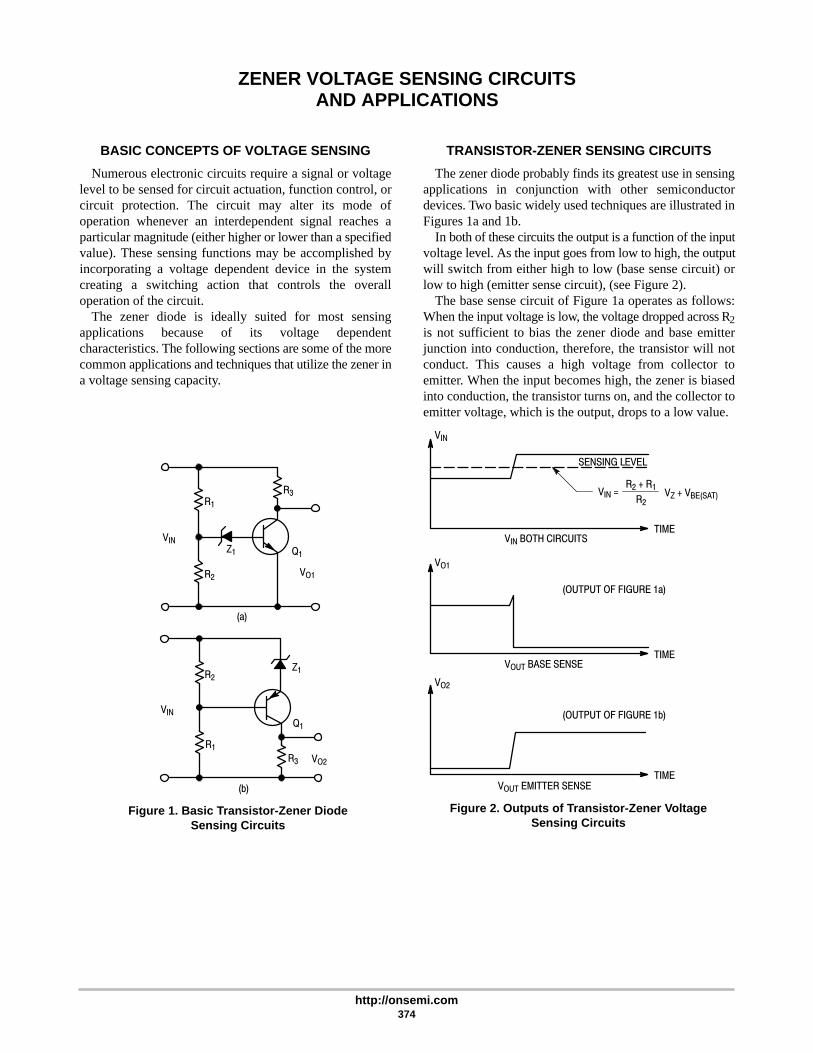
http://onsemi.com374
ZENER VOLTAGE SENSING CIRCUITSAND APPLICATIONS
BASIC CONCEPTS OF VOLTAGE SENSING
Numerous electronic circuits require a signal or voltagelevel to be sensed for circuit actuation, function control, orcircuit protection. The circuit may alter its mode ofoperation whenever an interdependent signal reaches aparticular magnitude (either higher or lower than a specifiedvalue). These sensing functions may be accomplished byincorporating a voltage dependent device in the systemcreating a switching action that controls the overalloperation of the circuit.
The zener diode is ideally suited for most sensingapplications because of its voltage dependentcharacteristics. The following sections are some of the morecommon applications and techniques that utilize the zener ina voltage sensing capacity.
Figure 1. Basic Transistor-Zener DiodeSensing Circuits
R2
R1
R3
R1
R2Z1
R3
VIN
VINZ1 Q1
Q1
VO1
VO2
(a)
(b)
TRANSISTOR-ZENER SENSING CIRCUITS
The zener diode probably finds its greatest use in sensingapplications in conjunction with other semiconductordevices. Two basic widely used techniques are illustrated inFigures 1a and 1b.
In both of these circuits the output is a function of the inputvoltage level. As the input goes from low to high, the outputwill switch from either high to low (base sense circuit) orlow to high (emitter sense circuit), (see Figure 2).
The base sense circuit of Figure 1a operates as follows:When the input voltage is low, the voltage dropped across R2is not sufficient to bias the zener diode and base emitterjunction into conduction, therefore, the transistor will notconduct. This causes a high voltage from collector toemitter. When the input becomes high, the zener is biasedinto conduction, the transistor turns on, and the collector toemitter voltage, which is the output, drops to a low value.
Figure 2. Outputs of Transistor-Zener VoltageSensing Circuits
R2 + R1
R2VZ + VBE(SAT)VIN =
SENSING LEVEL
TIME
TIME
TIME
VIN BOTH CIRCUITS
VOUT BASE SENSE
VOUT EMITTER SENSE
VO2
VO1
VIN
(OUTPUT OF FIGURE 1b)
(OUTPUT OF FIGURE 1a)

http://onsemi.com375
The emitter sense circuit of Figure 1b operates as follows:When the input is low the voltage drop across R3 (the output)is negligible. As the input voltage increases the voltage dropacross R2 biases the zener into conduction and forwardbiases the base-emitter junction. A large voltage drop acrossR3 (the output voltage) is equal to the product of the collectorcurrent times the resistance, R3. The following relationshipsindicate the basic operating conditions for the circuits inFigure 1.
Circuit Output
1a
1b
HighVOUT = VIN – ICOR3 ≅ VIN
LowVOUT = VIN – ICR3 = VCE(sat)
LowVOUT = VIN – VZ – VCE(off) = ICOR3
HighVOUT = VIN – VCE(sat) = ICR3
In addition, the basic circuits of Figure 1 can be rearrangedto provide inverse output.
AUTOMOTIVE ALTERNATOR VOLTAGEREGULATOR
Electromechanical devices have been employed for manyyears as voltage regulators, however, the regulation setting
of these devices tend to change and have mechanical contactproblems. A solid state regulator that controls the charge rateby sensing the battery voltage is inherently more accurateand reliable. A schematic of a simplified solid state voltageregulator is shown in Figure 3.
The purpose of an alternator regulator is to control thebattery charging current from the alternator. The chargelevel of the battery is proportional to the battery voltagelevel. Consequently, the regulator must monitor the batteryvoltage level allowing charging current to pass when thebattery voltage is low. When the battery has attained theproper charge the charging current is switched off. In thecase of the solid state regulator of Figure 3, the chargingcurrent is controlled by switching the alternator field currenton and off with a series transistor switch, Q2. The switchingaction of Q2 is controlled by a voltage sensing circuit that isidentical to the base sense circuit of Figure 1a. Whenunder-charged, the zener Z1 does not conduct keeping Q1off. The collector-emitter voltage of Q1 supplies a forwardbias to the base-emitter of Q2, turning it on. With Q2 turnedon, the alternator field is energized allowing a chargingcurrent to be delivered to the battery. When the batteryattains a proper charge level, the zener conducts causing Q1to turn on, and effectively shorting out the base-emitterjunction of Q2. This short circuit cuts off Q2, turns off thecurrent flowing in the field coil which consequently, reducesthe output of the alternator. Diode D1 acts as a fieldsuppressor preventing the build up of a high induced voltageacross the coil when the coil current is interrupted.
Figure 3. Simplified Solid State Voltage Regulator
R3
R1
R2
R4
B+
Z1 Q1
Q2
ALTERNATOROUTPUT
D1ALTERNATORFIELD

http://onsemi.com376
In actual operation, this switching action occurs manytimes each second, depending upon the current drain fromthe battery. The battery charge, therefore, remainsessentially constant and at the maximum value for optimumoperation.
A schematic of a complete alternator voltage regulator isshown in Figure 4.
It is also possible to perform the alternator regulationfunction with the sensing element in the emitter of thecontrol transistor as shown in Figure 5.
In this configuration, the sensing circuit is composed of Z1and Q1 with biasing components. It is similar to the sensingcircuit shown in Figure 1b. The potentiometer R1 adjusts theconduction point of Q1 establishing the proper charge level.When the battery has reached the desired level, Q1 begins toconduct. This draws Q2 into conduction, and thereforeshorts off Q3 which is supplying power to the alternatorfield. This type of regulator offers greater sensitivity with anincrease in cost.
Figure 4. Complete Solid State Alternator Voltage Regulator
Figure 5. Alternator Regulator with Emitter Sensor
B+
100 Ω
15 Ω
30 Ω
30 Ω
70 Ω
1N961BSENSINGZENERDIODE
RT*THERMISTOR
0.05 µFFEEDBACKCAPACITOR
1N4001FIELDSUPPRESSIONDIODE
TO ALTERNATORFIELD COIL
2N5879
1N3493BIASDIODE
ALTERNATOROUTPUT
0.05 Ω
2N4234
*THE VALUE OF RT DEPENDS ON THE SLOPE OF THE VOLTAGE REGULATIONVERSUS TEMPERATURE CURVE.
B+ ALTERNATOROUTPUT
D2
D1
Q3
R5
R4
Q2
R6
Z1
Q1
R3
R1
R2ALTERNATORFIELD
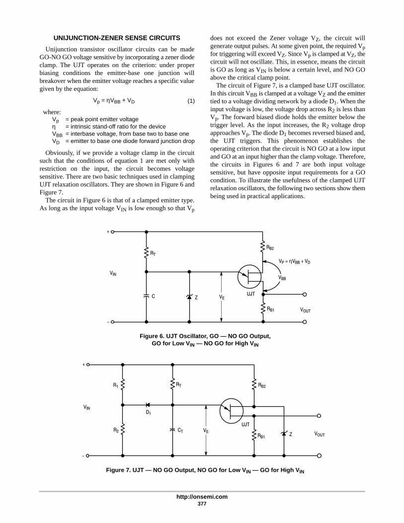
http://onsemi.com377
UNIJUNCTION-ZENER SENSE CIRCUITS
Unijunction transistor oscillator circuits can be madeGO-NO GO voltage sensitive by incorporating a zener diodeclamp. The UJT operates on the criterion: under properbiasing conditions the emitter-base one junction willbreakover when the emitter voltage reaches a specific valuegiven by the equation:
Vp = ηVBB + VD (1)
where:VpηVBBVD
= peak point emitter voltage= intrinsic stand-off ratio for the device= interbase voltage, from base two to base one= emitter to base one diode forward junction drop
Obviously, if we provide a voltage clamp in the circuitsuch that the conditions of equation 1 are met only withrestriction on the input, the circuit becomes voltagesensitive. There are two basic techniques used in clampingUJT relaxation oscillators. They are shown in Figure 6 andFigure 7.
The circuit in Figure 6 is that of a clamped emitter type.As long as the input voltage VIN is low enough so that Vp
does not exceed the Zener voltage VZ, the circuit willgenerate output pulses. At some given point, the required Vpfor triggering will exceed VZ. Since Vp is clamped at VZ, thecircuit will not oscillate. This, in essence, means the circuitis GO as long as VIN is below a certain level, and NO GOabove the critical clamp point.
The circuit of Figure 7, is a clamped base UJT oscillator.In this circuit VBB is clamped at a voltage VZ and the emittertied to a voltage dividing network by a diode D1. When theinput voltage is low, the voltage drop across R2 is less thanVp. The forward biased diode holds the emitter below thetrigger level. As the input increases, the R2 voltage dropapproaches Vp. The diode D1 becomes reversed biased and,the UJT triggers. This phenomenon establishes theoperating criterion that the circuit is NO GO at a low inputand GO at an input higher than the clamp voltage. Therefore,the circuits in Figures 6 and 7 are both input voltagesensitive, but have opposite input requirements for a GOcondition. To illustrate the usefulness of the clamped UJTrelaxation oscillators, the following two sections show thembeing used in practical applications.
Figure 6. UJT Oscillator, GO — NO GO Output,GO for Low V IN — NO GO for High V IN
+
-
RT
C ZUJT
RB2
RB1
VP = ηVBB + VD
VOUT
VIN
VE
VBB
Figure 7. UJT — NO GO Output, NO GO for Low V IN — GO for High V IN
Z
R1
R2
+
-
RT RB2
RB1
CT
D1
VIN
VOUT
UJTVE

http://onsemi.com378
BATTERY VOLTAGE SENSITIVE SCR CHARGER
A clamped emitter unijunction sensing circuit of the typeshown in Figure 6 makes a very good battery charger(illustrated in Figure 8). This circuit will not operate until thebattery to be charged is properly connected to the charger.The battery voltage controls the charger and will dictate itsoperation. When the battery is properly charged, the chargerwill cease operation.
The battery charging current is obtained through thecontrolled rectifier. Triggering pulses for the controlledrectifier are generated by unijunction transistor relaxationoscillator (Figure 9). This oscillator is activated when thebattery voltage is low.
While operating, the oscillator will produce pulses in thepulse transformer connected across the resistance, RGC(RGC represents the gate-to-cathode resistance of thecontrolled rectifier), at a frequency determined by theresistance, capacitance, R.C. time delay circuit.
Since the base-to-base voltage on the unijunctiontransistor is derived from the charging battery, it willincrease as the battery charges. The increase in base-to-basevoltage of the unijunction transistor causes its peak pointvoltage (switching voltage) to increase. These waveformsare sketched in Figure 9 (this voltage increase will tend tochange the pulse repetition rate, but this is not important).
Figure 8. 12 Volt Battery Charger Control
Figure 9. UJT Relaxation Oscillator Operation
RECTIFIED A.C.VOLTAGE FROMCHARGER
R3
C1
UJT
E B2R2
A C
GSCR
V
12 V
-
T1
B1
R1 3.9K, 1/2 W
R2 1K, POT.
R3 5.1K, 1/2 W
C1 .25 µf
Z1 1N753, 6.2 V
SCR MCR3813
VB1 B2
BATTERY
CHARGING
BATTERY
CHARGED
Z1
R1
R2
C1
TIME
TIME
TIME
VC1
VRGC
ZENER
VOLTAGE
UJT PEAK
POINT VOLTAGE
SCR
CONDUCTS
SCR
NONCONDUCTING
UJT B2
B1
RGCT1
VBATT.
+
UJT 2N2646
T1 PR1, 30T, no. 22
SEC, 45T, NO. 22
CORE: FERROX CUBE
203F181303
A+
R1
Z1

http://onsemi.com379
When the peak point voltage (switching voltage) of theunijunction transistor exceeds the breakdown voltage of theZener diode, Z1, connected across the delay circuitcapacitor, C1, the unijunction transistor ceases to oscillate.If the relaxation oscillator does not operate, the controlledrectifier will not receive trigger pulses and will not conduct.This indicates that the battery has attained its desired chargeas set by R2.
The unijunction cannot oscillate unless a voltagesomewhere between 3 volts and the cutoff setting is presentat the output terminals with polarity as indicated. Therefore,the SCR cannot conduct under conditions of a short circuit,an open circuit, or a reverse polarity connection to thebattery.
ALTERNATOR REGULATOR FORPERMANENT MAGNET FIELD
In alternator circuits such as those of an outboard engine,the field may be composed of a permanent magnet. Thisincreases the problem of regulating the output by limitingthe control function to opening or shorting the output.Because of the high reactance source of most alternators,opening the output circuit will generally stress the bridgerectifiers to a very high voltage level. It is, therefore,apparent that the best control function would be shorting theoutput of the alternator for regulation of the charge to thebattery.
Figure 10 shows a permanent magnet alternator regulatordesigned to regulate a 15 ampere output. The two SCRs areconnected on the ac side of the bridge, and short out thealternator when triggered by the unijunction voltagesensitive triggering circuit. The sensing circuit is of the typeshown in Figure 7. The shorted output does not appreciablyincrease the maximum output current level.
A single SCR could be designed into the dc side of thebridge. However, the rapid turn-off requirement of this typeof circuit at high alternator speeds makes this circuitimpractical.
The unijunction circuit in Figure 10 will not oscillate untilthe input voltage level reaches the voltage determined by theintrinsic standoff ratio. The adjustable voltage divider willcalibrate the circuit. The series diode in the voltage dividercircuit will compensate for the emitter-base-one diodetemperature change, consequently, temperaturecompensation is necessary only for the zener diodetemperature changes.
Due to the delay in charging the unijunction capacitor,when the battery is disconnected the alternator voltage willproduce high stress voltage on all components before theSCRs will be fired. The 1N971B Zener was included in thecircuit to provide a trigger pulse to the SCRs as soon as thealternator output voltage level approaches 30 volts.
Figure 10. Permanent Magnet Field Alternator Regulator
SE
C. 1
SE
C. 2
PR
I.
MCR23042
ALT.OUT MCR
23042
MDA2500
1N960B
200 Ω 5K Ω 27 Ω
0.1 µF
2N2646
1N971B
T1
1N4001200 Ω
27 Ω
BATTERY+
T1
CORE: ARNOLD no. 4T5340 D1 DD1
PRIMARY 125 TURNSAWG 36
SEC no. 1 125 TURNSAWG 36
SEC no. 2 125 TURNSAWG 36
TRIFILAR WOUND
+

http://onsemi.com380
Figure 11. Zener-Resistor Voltage Sensitive Circuit
Figure 12. Improving Meter Resolution
+
-
Z
R
BASE CIRCUIT
VZ
+ +
VIN VOUT VIN VOUT
(LEVEL DETECTION) (MAGNITUDE REDUCTION)
Z
R
+
-
+
-
VZ = 20 V
VOLTMETER10 V FULL SCALE
TYPICAL OUTPUTS
VIN VOUT
VIN = 24 V - 28 V
ZENER-RESISTOR VOLTAGE SENSING
A simple but useful sense circuit can be made from just aZener diode and resistor such as shown in Figure 11.
Whenever the applied signal exceeds the specific Zenervoltage VZ, the difference appears across the droppingresistor R. This level dependent differential voltage can beused for level detection, magnitude reduction, waveshaping, etc. An illustrative application of the simple seriesZener sensor is shown in Figure 12, where the resistor dropis monitored with a voltmeter.
If, for example, the input is variable from 24 to 28 volts,a 30 voltmeter would normally be required. Unfortunately,a 4 volt range of values on a 30 volt scale utilizes only 13.3%of the meter movement — greatly limiting the accuracy with
which the meter can be read. By employing a 20 volt zener,one can use a 10 voltmeter instead of the 30 volt unit, therebyutilizing 40% of the meter movement instead of 13.3% witha corresponding increase in accuracy and readability. Forultimate accuracy a 24 volt zener could be combined with a5 voltmeter. This combination would have the disadvantageof providing little room for voltage fluctuations, however.
In Figure 13, a number of sequentially higher-voltageZener sense circuits are cascaded to actuate transistorswitches. As each goes into avalanche its respectiveswitching transistor is turned on, actuating the indicatorlight for that particular voltage level. This technique can beexpanded and modified to use the zener sensors to actuatesome form of logic system.
Figure 13. Sequential Voltage Level Indicator
Z1
Q1 Q2 Q3
R1 R2 R3RE2RE1 RE3
Z2 Z3LIGHT
(1)
LIGHT
(2)
LIGHT
(3)
INPUT OUTPUT

http://onsemi.com381
MISCELLANEOUS APPLICATIONSOF ZENER TYPE DEVICES
INTRODUCTION
Many of the commonly used applications of zener diodeshave been illustrated in some depth in the precedingchapters. This chapter shows how a zener diode may be usedin some rarer applications such as voltage translators, toprovide constant current, wave shaping, frequency controland synchronized SCR triggers.
The circuits used in this chapter are not intended asfinished designs since only a few component values aregiven. The intent is to show some general broad ideas andnot specific designs aimed at a narrow use.
FREQUENCY REGULATION OF ADC TO AC INVERTER
Zener diodes are often used in control circuits, usually tocontrol the magnitude of the output voltage or current. In thisunusual application, however, the zener is used to control theoutput frequency of a current feedback inverter. The circuitis shown in Figure 1.
Figure 1. Frequency Controlled CurrentFeedback Inverter
Z1
Q1
Q2
T1
NC
N6
N6
NC
B1
B2
+
A
-
N1
N1
N2
T2
LOAD
The transformer T1 functions as a current transformerproviding base current IB = (NC/NB)IC. Without the zener
diode, the voltage across NB windings of the timingtransformer T1 is clamped to VBE of the ON device, givingan inverter frequency of
f =VBE x 108
4BS1A1NB
where BS1A1 is the flux capacity of T1 transformer core.The effect on output frequency of VBE variations due tochanging load or temperature can be reduced by using azener diode in series with VBE as shown in Figure 1. Forthis circuit, the output frequency is given by
f =(VBE + VZ) x 108
4BS1A1NB
If V BE is small compared to the zener voltage VZ, goodfrequency accuracy is possible. For example, with VZ =9.1 volts, a 40 Watt inverter using 2N3791 transistors(operating from a 12 volt supply), exhibited frequencyregulation of ±2% with ±25% load variation.
Care should be taken not to exceed V(BR)EBO of thenon-conducting transistor, since the reverse emitter-basevoltage will be twice the introduced series voltage, plus VBEof the conducting device.
Transformer T2 should not saturate at the lowest inverterfrequency.
Inverter starting is facilitated by placing a resistor frompoint A to B1 or a capacitor from A to B2.
SIMPLE SQUARE WAVE GENERATOR
The zener diode is widely used in wave shaping circuits;one of its best known applications is a simple square wavegenerator. In this application, the zener clips sinusoidalwaves producing a square wave such as shown in Figure 2a.In order to generate a wave with reasonably vertical sides,the ac voltage must be considerably higher than the zenervoltage.
Clipper diodes with opposing junctions built into thedevice are ideal for applications of the type shown inFigure 2b.

http://onsemi.com382
(a) Single Zener Diode Square Wave Generator
(b) Opposed Zener Diodes Square Wave Generator
Figure 2. Zener Diode Square Wave Generator
Z1
Z
Z2
R
R
ZENER
VOLTAGE
FORWARD
DROP
VOLTAGE
ZENER Z1
VOLTAGE
ZENER Z2
VOLTAGE
A.C. INPUT OUTPUT
A.C. INPUT OUTPUT

http://onsemi.com383
TRANSIENT VOLTAGE SUPPRESSION
INTRODUCTIONElectrical transients in the form of voltage surges have
always existed in electrical distribution systems, and prior tothe implementation of semiconductor devices, they were ofminor concern. The vulnerability of semiconductors tolightning strikes was first studied by Bell Laboratories in1961.1 A later report tried to quantify the amount of energycertain semiconductors could absorb before they sufferedlatent or catastrophic damage from electrostatic discharge.2
Despite these early warnings, industry did not begin toaddress the issue satisfactorily until the late 1970s. Listedbelow are the seven major sources of overvoltage.
• Lightning• Sunspots• Switching of Loads in Power Circuits• Electrostatic Discharge• Nuclear Electromagnetic Pulses• Microwave Radiation• Power Cross
Most electrical and electronic devices can be damaged byvoltage transients. The difference between them is theamount of energy they can absorb before damage occurs.Because many modern semiconductor devices, such assmall signal transistors and integrated circuits can bedamaged by disturbances that exceed the voltage ratings atonly 20 volts or so, their survivability is poor in unprotectedenvironments.
In many cases, as semiconductors have evolved theirruggedness has diminished. The trend to produce smallerand faster devices, and the advent of MOSFET and galliumarsenide FET technologies has led to an increasedvulnerability. High impedance inputs and small junctionsizes limit the ability of these devices to absorb energy andto conduct large currents. It is necessary, therefore, tosupplement vulnerable electronic components with devicesspecially designed to cope with these hazards. Listed beloware the four primary philosophies for protecting againsttransients.
• Clamping, or “clipping” is a method of limiting theamplitude of the transient.
• Shunting provides a harmless path for the transient,usually to ground by way of an avalanche or a crowbarmechanism.
• Interrupting opens the circuit for the duration of thetransient.
• Isolating provides a transient barrier between hostileenvironments and vulnerable circuits through the use oftransformers or optoisolators.
Selection of the proper protective method should be madebased upon a thorough investigation of the potential sourcesof the overvoltage hazard. Different applications andenvironments present different sources of overvoltage.
LIGHTNINGAt any given time there are about 1800 thunderstorms in
progress around the world, with lightning striking about 100times each second. In the U.S., lightning kills about 150people each year and injures another 250. In flat terrain withan average lightning frequency, each 300 foot structure willbe hit, on average, once per year. Each 1200 foot structure,such as a radio or TV tower, will be hit 20 times each year,with strikes typically generating 600 million volts.
Each cloud-to-ground lightning flash really contains fromthree to five distinct strokes occurring at 60 ms intervals,with a peak current of some 20,000 amps for the first strokeand about half that for subsequent strokes. The final strokemay be followed by a continuing current of around 150 ampslasting for 100 ms.
The rise time of these strokes has been measured at around200 nanoseconds or faster. It is easy to see that thecombination of 20,000 amps and 200 ns calculates to a valueof dI/dt of 1011 amps per second! This large value means thattransient protection circuits must use RF design techniques,particularly considerate of parasitic inductance andcapacitance of conductors.
While this peak energy is certainly impressive, it is reallythe longer-term continuing current which carries the bulk ofthe charge transferred between the cloud and ground. Fromvarious field measurements, a typical lightning model hasbeen constructed, as shown in Figure 1.
Figure 1. Typical Lightning Model, with and withoutContinuing Current
Flash with Continuing Current
Flash with No Continuing Current
40 µs
6060
TIME (ms)
TIME (ms)
60 0.3 100
150 A

http://onsemi.com384
Depending on various conditions, continuing current mayor may not be present in a lightning strike. A severe lightningmodel has also been created, which gives an indication of thestrength which can be expected during worst case conditionsat a point very near the strike location. Figure 2 shows thismodel. Note that continuing current is present at more thanone interval, greatly exacerbating the damage which can beexpected. A severe strike can be expected to ignitecombustible materials.
Figure 2. Severe Lightning Model
460 8607006405805201601106010
400 A
200 A
TIME (ms)
A direct hit by lightning is, of course, a dramatic event. Infact, the electric field strength of a lightning strike nearbymay be enough to cause catastrophic or latent damage tosemiconductor equipment. It is a more realistic venture to tryto protect equipment from these nearby strikes than toexpect survival from a direct hit.
With this in mind, it is important to be able to quantify theinduced voltage as a function of distance from the strike.Figure 3 shows that these induced voltages can be quite high,explaining the destruction of equipment from relativelydistant lightning flashes.
Figure 3. Voltage Induced by NearbyLightning Strike
10000
1000
100
10
11010.1
DISTANCE FROM STRIKE (km)
IND
UC
ED
VO
LTA
GE
IN 1
m O
F W
IRE
(V
)Burying cables does not provide appreciable protection as
the earth is almost transparent to lightning radiated fields. Infact, underground wiring has a higher incidence of strikesthan aerial cables.3
SUNSPOTSThe sun generates electromagnetic waves which can
disrupt radio signals and increase disturbances on residentialand business power lines. Solar flares, which run in cyclesof 11 years (1989 was a peak year) send out electromagneticwaves which disrupt sensitive equipment.
Although not quantified, the effects of sunspot activityshould be considered. Sunspots may be the cause ofsporadic, and otherwise unexplainable problems in suchsensitive areas.
SWITCHING OF LOADS IN POWER CIRCUITSInductive switching transients occur when a reactive load,
such as a motor or a solenoid coil, is switched off. Therapidly collapsing magnetic field induces a voltage acrossthe load’s winding which can be expressed by the formula:
V = –L (dI/dt)where L is inductance in henrys and dI/dt is the rate ofchange of current in amps per second.
Such transients can occur from a power failure or thenormal opening of a switch. The energy associated with thetransient is stored within the inductance at powerinterruption and is equal to:
W = 1/2 Li2
where W is energy in joules and i is instantaneous current inamps at the time of interruption.
As an example, a 1.4 to 2.5 kV peak transient can beinjected into a 120 vac power line when the ignition systemof an oil furnace is fired. It has also been shown that there aretransients present on these lines which can reach as high as6 kV. In locations without transient protection devices, themaximum transient voltage is limited to about 6 kV by theinsulation breakdown of the wiring.
Inductive switching transients are the silent killers ofsemiconductors as they often occur with no outwardindication. A graphic example is the report of a largeelevator company indicating the failure of 1000 voltrectifiers during a power interruption. In another area, powerinterruption to a 20 HP pump motor in a remote area wasdirectly related to failure of sensitive monitoring equipmentat that same site.4

http://onsemi.com385
Figure 4. Switching Transient Definition for Aircraftand Military Buses, per Boeing Document D6-16050
28 VdcB A
WAVEFORM AT POINT A
TIME (µs)
V
t1t2
V = 600 V pk-pkNo. of Repetitions = 5 to 100
t1 = 0.2 to 10 µst2 = 50 to 1000 µs
After characterizing electrical overstress on aircraftpower buses, Boeing published Document D6-16050 asshown in Figure 4.
The military has developed switching transientdefinitions within several specifications including:
DOD-STD-1399 for shipboardMIL-STD-704 for aircraftMIL-STD-1275 for ground vehicles
The International Electrotechnical Commission (IEC) isnow promoting their specification IEC 801-4 throughoutthe European community. This describes an inductiveswitching transient voltage threat having 50 ns wide spikeswith amplitudes from 2 kV to 4 kV occurring in 300 ms widebursts.5
Besides these particular military specifications, many areapplication specific and functional tests exist. A supplier oftransient voltage suppressor components will be expected toperform to a wide variety of them.
ELECTROSTATIC DISCHARGE (ESD)ESD is a widely recognized hazard during shipping and
handling of many semiconductor devices, especially thosethat contain unprotected MOSFETs, semiconductors for useat microwave frequencies and very high speed logic withswitching times of 2 ns or less. In response to this threat,most semiconductors are routinely shipped in containersmade of conductive material.
In addition to various shipping precautions, electronicassembly line workers should be grounded, usegrounded-tip soldering irons, ionized air blowers and othertechniques to prevent large voltage potentials to begenerated and possibly discharged into the semiconductorsthey are handling.
Once the assembled device is in normal operation, ESDdamage can still occur. Any person shuffling his feet on acarpet and then touching a computer keyboard can possiblycause a software crash or, even worse, damage the keyboardelectronics.
The electrical waveform involved in ESD is a brief pulse,with a rise time of about 1 ns, and a duration of 100–300 µs.The peak voltage can be as large as 30 kV in dry weather, butis more commonly 0.5–5.0 kV.6 The fastest rise times occurfrom discharges originating at the tip of a hand-held tool,while discharges from the finger tip and the side of the handare slightly slower.7 A typical human with a bodycapacitance of 150 pF, charged to 3 microcoulombs, willdevelop a voltage potential of 20 kV, according to theformula:
V = Q / C
where V is voltage, Q is charge and C is capacitance. Theenergy delivered upon discharge is:
W = 1/2 CV2
where W is energy in joules, C is capacitance and V isvoltage.
It is interesting to note that most microcircuits can bedestroyed by a 2500 volt pulse, but a person cannot feel astatic spark of less than 3500 volts!
NUCLEAR ELECTROMAGNETIC PULSES (NEMP)When a nuclear weapon is detonated, a very large flux of
photons (gamma rays) is produced. These rays act toproduce an electromagnetic field known as a nuclearelectromagnetic pulse or NEMP. When a nuclear detonationoccurs above the atmosphere, a particulary intense pulseilluminates all objects on the surface of the earth, and allobjects in the lower atmosphere within line of sight of theburst. A burst 300–500 km above Kansas would illuminatethe entire continental U.S.
A typical NEMP waveform is a pulse with a rise time ofabout 5 ns and a duration of about 1 µs. Its peak electric fieldis 50–100 kV/m at ground level. After such a pulse iscoupled into spacecraft, aircraft and ground supportequipment, it produces a waveform as described inMIL-STD-461C . The insidious effect of NEMP is its broadcoverage and its potential for disabling military defensesystems.
MICROWAVE RADIATIONMicrowaves can be generated with such high power that
they can disable electronic hardware upon which manymilitary systems depend. A single pulse flux of 10–8 MJ/cm2
burns out receiver diodes, and a flux of 10–4 MJ/cm2 causesbit errors in unshielded computers.8 With automobilesutilizing MPU controls in more applications, it is importantto protect against the effects of driving by a microwavetransmitter. Likewise, a nearby lightning strike could alsohave detrimental effects to these systems.
POWER CROSSYet another source of electrical overstress is the accidental
connection of signal lines, such as telephone or cabletelevision, to an ac or dc power line. Strictly speaking, thisphenomenon, known as a power cross, is a continuous state,not a transient. However, the techniques for ensuring the

http://onsemi.com386
survival of signal electronics after a power cross are similarto techniques used for protection against transientovervoltages.
STANDARDIZED WAVEFORMSFortunately, measurements of these hazards have been
studied and documented in several industry specifications.For example, Bellcore Technical AdvisoryTA-TSY-000974 defines the generic measurementwaveform for any double exponential waveform, which isthe basis for most of the specific applications norms.
The predominant waveform for induced lightningtransients, set down by Rural Electrification AdministrationDocument PE-60, is shown in Figure 5. This pulse test,performed at the conditions of 100 V/µs rise, 10/1000 µs, Ip= 1 kV, is one of the two most commonly specified in theindustry. The other is the 8/20 µs waveform, shown inFigure 6.
Figure 5. Pulse Waveform (10/1000 µs)
Figure 6. Pulse Waveform (8/20 µs)
3020100
lp.9 lp
.5 lp
.1 lp
TIME, µs
1 2 3
.1 Ip
.5 Ip
.9 IpIp
0
TIME, ms
TRANSIENT VOLTAGE SUPPRESSIONAND TELECOM
TRANSIENT VOLTAGE SURGE SUPPRESSIONCOMPONENTS ON DATA AND TELEPHONE LINES
Lines carrying data and telephone signals are subject to anumber of unwanted and potentially damaging transientsprimarily from two sources: lightning and “power crosses.”A power cross is an accidental connection of a signal line toa powerline. Transients from lightning can impress voltageswell above a kilovolt on the line but are of short duration,usually under a millisecond. Lightning transients aresuppressed by using Transient Voltage Surge Suppressor
(TVS) devices. TVS devices handle high peak currentswhile holding peak voltage below damaging levels, but haverelatively low energy capability and cannot protect againsta power cross fault. The first TVS used by telephonecompanies is the carbon block, but its peak let-throughvoltage was too high for modern equipment usingunprotected solid state circuitry. A number of othercomponents fill today’s needs.
The power cross condition causes a problem withtelephone lines. Fast acting fuses, high speed circuitbreakers and positive temperature coefficient thermistorshave been successfully used to limit or interrupt currentsurges exceeding a millisecond.
Over the years, telecommunications switching equipmenthas been transitioning from electromechanical relays tointegrated circuits and MOSFET technology. The newerequipment operates at minimal electrical currents andvoltages, which make it very efficient. It is therefore quitesensitive to electrical overloads caused by lightning strikesand other transient voltage sources, and by power crosses.
Because of the deployment of new technology, both innew installations and in the refurbishment of older systems,the need for transient protection has grown rapidly. It iswidely recognized that any new equipment must includeprotection devices for reasons of safety, reliability and longterm economy.
The major telecom companies, in their never ending questfor the elimination of electromechanical technology havebeen looking at a number of novel methods andimplementations of protection. These methods provide forsolutions to both the primary and secondary protectioncategories.
A number of studies have been conducted to determine thetransient environment on telephone lines. Very little hasbeen done with data lines because a typical situation does notexist. However, information gathered from telephone linestudies can serve as a guide for data lines.
Past studies on telephone lines coupled with the highcurrent capability of arc type arrestors and the conservativenature of engineers seem to have produced specificationswhich far exceed the real need. A recent study by Bell SouthServices9 reported that the highest level of transient energyencountered was well below standards and specifications incommon use. Now, solid state devices perform adequatelyfor many applications. However the stringent specificationsof some regulatory agencies promote arc-type arrestors,though solid state devices would be a better choice.
PRIMARY PROTECTION
Primary protection is necessary to protect against highvoltage transients which occur in the outdoor environment.These transients include induced lightning surges and accross conditions.
As such, primary protection is located at the point wherewiring enters the building or terminal box. It is the first linedefense against outside hazards. TVS devices located wherelines enter a building are called primary protectors.

http://onsemi.com387
Protectors connected to indoor lines are referred to assecondary protectors. Both primary and secondaryprotectors are required to provide complete equipmentprotection.
Today, primary protection is most generally accomplishedthrough the use of surge protector modules. For telecom,these are designed specifically for the environment and thestandards dictated by the telecom applications. Theytypically contain a two or three element gas arrestor tube anda mechanically-triggered heat coil. Some also include airgap carbon block arrestors which break over at voltagesabove about 1500 volts.
Some modules contain high speed diodes for clampresponse in the low nanoseconds. This provides protectionuntil the gas tube fires, generally in about one microsecond.The diodes may be connected between the tip, ring andground conductors in various combinations. The 5ESSelectronic switching system norms dictate design andperformance requirements of TVS modules in use today.Test methods are spelled out in REA PE-80, a publicationof the Rural Electrification Administration.
In the U.S. alone, 58 million primary protection modulesare sold annually, about 40 million for central offices and 18million for station locations, such as building entrances.Eighty percent of these use gas tubes, 16% use air-gapcarbon blocks, and only 2% (so far) are solid state.
SECONDARY PROTECTION
Secondary protection is necessary for the equipmentinputs, and as such, is located between the primary protectorand the equipment. Secondary protection is generallyaccomplished with one or more TVS components, asopposed to the modules used for primary. It is often placedon a circuit board along with other components handlingother duties, such as switching. Secondary protection isapplied to lines associated with long branch circuits whichhave primary protection a significant distance away, tointernal data lines, and to other locations requiringadditional local hazard-proofing.
While not as open to external transients as the primary,secondary can still see peak open circuit voltages in excessof 1000 volts and short circuit currents of hundreds of amps.These transients may be locally generated, or they may beresiduals from the primary protectors upstream.
STANDARDS
Transient voltage waveforms are commonly described interms of a dual exponential wave as defined in Figure 7. Thestandard chosen for power lines is a 1.2/50 µs voltage wavewhich causes an 8/20 µs current wave. Although the sourceof the most severe transients on telecom lines is the same asfor power lines and lightning, the higher impedance per unitlength of the telephone line stretches the waves as theypropagate through the lines.
Figure 7. Definition of Double ExponentialImpulse Waveform
P0.9 P
0.5 P
0.1 P
T0
a b T1 T2TIME
WAVEFORM IS DEFINED AS tr/tdWHERE
tr : FRONT TIME = 1.25 (ba)
= (T1T0)
td : DURATION = (T2T0)
The 10/1000 µs wave approximates the worst casewaveform observed on data and telecom lines. TVS devicesintended for this service are usually rated and characterizedusing a 10/1000 waveform. The Bell South study revealedthat the worst transient energy handled by primaryprotectors on lines entering a central office was equivalentto only 27 A peak of a 10/1000 wave. This level isconsiderably less than that required by secondary protectorsin most of the standards in use today. This finding isparticularly significant because the Bell South service areaincludes Central Florida, the region experiencing the highestlightning activity in the U.S.
The United States Federal Communications Commission(FCC) has defined mandatory requirements for equipmentwhich is to be connected to the U.S. telephone network. Insome cases, U.S. equipment must meet standards developedby the Rural Electrification Agency (REA). Many nationsdemand compliance to standards imposed by theConsultative Committee, International Telegraph andTelephone (CCITT). In addition, most equipment usersdemand safety certification from U.L., which has its ownstandards.
The FCC Standards are based on a worst case residue froma carbon block primary protector installed where the phoneline enters the building. The CCITT standard is applicablefor situations lacking primary protection, other than wiringflashover. Companies entering the telephone equipment orprotector market will need to obtain and become familiarwith the appropriate governing standards.
TRANSIENT VOLTAGE PROTECTIONCOMPONENTS
GENERAL TVS CHARACTERISTICS
A number of transient voltage suppressor (TVS) devicesare available. Each finds use in various applications basedupon performance and cost. All types are essentiallytransparent to the line until a transient occurs; however,some devices have significant capacitance which loads theline for ac signals. A few of the these are described inTable 1.
Based upon their response to an overvoltage, TVS devicesfit into two main categories, clamps and crowbars. A clampconducts when its breakdown voltage is exceeded andreverts back to an open circuit when the applied voltage

http://onsemi.com388
drops below breakdown. A crowbar switches into a lowvoltage, low impedance state when its breakover voltage isexceeded and restores only when the current flowingthrough it drops below a “holding” level.
CLAMP DEVICES
All clamp devices exhibit the general V-I characteristic ofFigure 8. There are variations; however, some clamps areasymmetric. In the non clamping direction, some devicessuch as the zener TVS exhibit the forward characteristic ofa diode while others exhibit a very high breakdown voltageand are not intended to handle energy of “reverse” polarity.Under normal operating conditions, clamp devices appearvirtually as an open circuit, although a small amount ofleakage current is usually present. With increasing voltagea point is reached where current increases rapidly withvoltage as shown by the curved portion of Figure 8. Therapidly changing curved portion is called the “knee region.”Further increases in current places operation in the“breakdown” region.
Figure 8. Static Characteristics of a Clamp Device
0
V
I O
In the knee region the V-I characteristic of clampingdevices can be approximated by the equation:
I = K Vs (1)
where K is a constant of proportionality and s is an exponentwhich defines the “sharpness factor” of the knee. Theexponent s is 1 for a resistor and varies from 5 to over 100for the clamping devices being used in TVS applications. Ahigh value of s i.e., a sharp knee, is beneficial. A TVS devicecan be chosen whose breakdown voltage is just above theworst case signal amplitude on the line without concern ofloading the line or causing excessive dissipation in the TVS.
As the current density in the clamp becomes high, theincremental resistance as described by Equation 1 becomesvery small in comparison to the bulk resistance of thematerial. The incremental resistance is therefore ohmic inthe high current region.
Unfortunately, a uniform terminology for all TVS deviceshas not been developed; rather, the terms were developed inconjunction with the appearance of each device in themarketplace. The key characteristics normally specifieddefine operation at voltages below the knee and at currentsabove the knee.
Leakage current is normally specified below the knee ata voltage variously referred to as the stand-off voltage, peakworking voltage or rated dc voltage. Some devices are ratedin terms of an RMS voltage, if they are bidirectional. Normalsignal levels must not exceed this working voltage if thedevice is to be transparent.
Breakdown voltage is normally specified at a fairly lowcurrent, typically 1 mA, which places operation past theknee region. Worst case signal levels should not exceed thebreakdown voltage to avoid the possibility of circuitmalfunction or TVS destruction.
The voltage in the high current region is called theclamping voltage, VC. It is usually specified at the maximumcurrent rating for the device. To keep VC close to thebreakdown voltage, s must be high and the bulk resistancelow. A term called clamping factor, (FC) is sometimes usedto describe the sharpness of the breakdown characteristic.FC is the ratio of clamping voltage to the breakdown voltage.As the V-I characteristic curve of the TVS approaches a rightangle, the clamping factor approaches unity. Clampingfactor is not often specified, but it is useful to describe clampdevice behavior in general terms.
Table 1. Comparison of TVS Components
TypeProtection
TimeProtection
VoltagePower
DissipationReliable
PerformanceExpected
LifeOther
Considerations
GAS TUBE > 1 µs 60–100 V Nil No Limited Only 50–2500 surges.Can short power line.
MOV 10–20 ns > 300 V Nil No Degrades Fusing required. Degrades.Voltage level too high.
AVALANCHE TVS 50 ps 3–400 V Low Yes Long Low power dissipation.Bidirectional requires dual.
THYRISTOR TVS < 3 ns 30–400 V Nil Yes Long High capacitance.Temperature sensitive.

http://onsemi.com389
Clamp devices generally react with high speed and as aresult find applications over a wide frequency spectrum. Nodelay is associated with restoration to the off state afteroperation in the breakdown region.
CROWBAR DEVICES
Crowbar TVS devices have the general characteristicsshown in Figure 9. As with clamp devices, asymmetriccrowbars are available which may show a diode forwardcharacteristic or a high voltage breakdown in one direction.
Figure 9. Static Characteristics of aBidirectional Crowbar Device
VD V3O2
VT
I2
I1
3
21
V3O1VT
The major difference between a crowbar and a clamp isthat, at some current in the breakdown region, the deviceswitches to a low voltage on-state. In the clamping regionfrom I1 to I2, the slope of the curve may be positive as shownby segment 1, negative (segment 2) or exhibit bothcharacteristics as shown by segment 3. A slightly positiveslope is more desirable than the other two curves because anegative resistance usually causes a burst of high frequencyoscillation which may cause malfunction in associatedcircuitry. However, a number of performance andmanufacturing trade-offs affect the shape of the slope in theclamping region.
A crowbar TVS has an important advantage over a clampTVS in that it can handle much larger transient surge currentdensities because the voltage during the surge isconsiderably lower. In a telephone line application, forexample, the clamping level must exceed the ring voltagepeak and will typically be in the vicinity of 300 volts duringa high current surge. The on-state level of the crowbar maybe as low as 3 volts for some types which allows about twoorders of magnitude increase in current density for the samepeak power dissipation.
However, a crowbar TVS becomes “latched” in theon-state. In order to turn off its current flow the drivingvoltage must be reduced below a critical level called theholding or extinguishing level. Consequently, in anyapplication where the on-state level is below the normalsystem voltage, a follow-on current occurs. In a dc circuitcrowbars will not turn off unless some means is provided tointerrupt the current. In an ac application crowbars will turnoff near the zero crossing of the ac signal, but a time delayis associated with turn-off which limits crowbars to
relatively low frequency applications. In a data line ortelecom application the turn-off delay causes a loss ofintelligence after the transient surge has subsided.
A telephone line has both ac and dc signals present.Crowbars can be successfully used to protect telecom linesfrom high current surges. They must be carefully chosen toensure that the minimum holding current is safely above themaximum dc current available from the lines.
TVS DEVICESA description of the various types of TVS devices follows
in the chronological order in which they became available.Used appropriately, sometimes in combination, anytransient protection problem can be suitably resolved. Theirsymbols are shown in Figure 10.
Figure 10. TVS Devices and Their Symbols
Air-GapCarbon Block
2- and 3-ElementGas Tubes
Heat CoilSwitch
Metal OxideVaristor (MOV)
ZenerRegulator
UnidirectionalAvalanche TVS De-
vice
BidirectionalAvalanche TVS Device
Thyristor TVS Devices Dual Thyristor TVS Devices
AIR GAP ARRESTORS
The air gap is formed by a pair of metal points rigidly fixedat a precise distance. The air ionizes at a particular voltagedepending upon the gap width between the points. As the airionizes breakover occurs and the ionized air provides a lowimpedance conductive path between the points.
The breakover threshold voltage is a function of the air’srelative humidity; consequently, open air gaps are usedmainly on high voltage power lines where preciseperformance is not necessary. For more predictablebehavior, air gaps sealed in glass and metal packages are alsoavailable.
Because a finite time is required to ionize the air, the actualbreakover voltage of the gap depends upon the rate of rise ofthe transient overvoltage. Typically, an arrestor designed fora 120 V ac line breaks over at 2200 volts.
Air gaps handle high currents in the range of 10,000amperes. Unfortunately, the arc current pits the tips whichcauses the breakover voltage and on-state resistance toincrease with usage.

http://onsemi.com390
CARBON BLOCK ARRESTORS
The carbon block arrestor, developed around the turn ofthe century to protect telephone circuits, is still in place inmany older installations. The arrestor consists of two carbonblock electrodes separated by a 3 to 4 mil air gap. The gapbreaks over at a fairly high level – approximately 1 kV – andcannot be used as a sole protection element for moderntelecom equipment. The voltage breakdown level isirregular. With use, the surface of the carbon block is burnedwhich increases the unit’s resistance. In addition, the burnedmaterial forms carbon tracks between the blocks causing aleakage current path which generates noise. Consequently,many of the carbon blocks in service are being replaced bygas tubes and are seldom used in new installations.
SILICON CARBIDE VARISTORS
The first non-linear resistor to be developed was called a“varistor.” It was made from specially processed siliconcarbide and found wide use in high power, high voltage TVSapplications. It is not used on telecom lines because itsclamping factor is too high: s is only about 5.
GAS SURGE ARRESTORS
Gas surge arrestors are a sophisticated modification of theair gap more suited to telecom circuit protection. Most oftenused is the “communication” type gap which measuresabout 3/8 inch in diameter and 1/4 inch thick. A cross sectionis shown in Figure 11. They consist of a glass or ceramicenvelope filled with a low pressure inert gas with specializedelectrodes at each end. Most types contain a minute quantityof radioactive material to stabilize breakover voltage.Otherwise, breakover is sensitive to the level of ambientlight.
Because of their small size and fairly wide gap,capacitance is very low, only a few picofarads. When notactivated, their off-state impedance or insulation resistanceis virtually infinite.
ÇÇÇÇÇÇÇÇÇÇÇÇÇÇÇÇÇÇÇÇÇÇÇÇÇÇÇÇÇÇÇÇÇÇÇÇÇÇÇÇÇÇÇÇÇÇÇÇÇÇÇÇÇÇÇÇÇÇÇÇ
ÇÇÇÇÇÇÇÇÇÇÇÇÇÇÇÇÇÇÇÇÇÇÇÇÇÇÇÇÇÇÇÇÇÇÇÇÇÇÇÇÇÇÇÇÇÇÇÇ
Figure 11. Gas Arrestor Cross Section
ELECTRODES
DISCHARGE
REGION
INSULATOR
(GLASS OR
CERAMIC MATERIAL)
ACTIVATING
COMPOUNDIGNITION AID
Key electrical specifications for this TVS type includebreakover voltage (dc & pulse), maximum holdovervoltage, arc voltage, and maximum surge current.
The breakover voltage is rated at a slow rate of rise,5000 V/s, essentially dc to a gas arrestor. Typical dc voltageratings range from 75 V through 300 V to provide for mostcommunication systems protection requirements. Themaximum pulse voltage rating is that level at which thedevice fires and goes into conduction when subjected to afairly rapid rate of voltage rise, (dv/dt) usually 100 V/µs.Maximum rated pulse voltages typically range from 400 Vto 600 V, depending on device type.
A typical waveform of a gas surge arrestor responding toa high voltage pulse is shown in Figure 12. From thewaveform, it can be seen that the dv/dt of the wave is 100v/µs and the peak voltage (the breakover voltage) is 520 V.
Figure 12. Voltage Waveform of Gas Surge ArrestorResponding to a Surge Voltage
AR
RE
STO
R V
OLT
AG
E (
VO
LTS
)
TIME (500 ns/DIVISION)
0
200
400
600
0 1 2 3
Gas surge arrestors fire faster but firing voltage increasesas the transient wave fronts increase in slope as illustrated inFigure 13. The near vertical lines represent the incidenttransient rise time. Note that the response time is greater than0.1s at slow rise times but decreases to less than 0.1 µs forrisetimes of 20 kV/µs. However, the firing voltage hasincreased to greater than 1000 V for the gas tube whichbreaks over at 250 Vdc.
The driving circuit voltage must be below the holdovervoltage for the gap to extinguish after the transient voltagehas passed. Holdover voltage levels are typically 60% to70% of the rated dc breakdown voltage.
Arc voltage is the voltage across the device duringconduction. It is typically specified at 5 to 10 V under a lowcurrent condition, but can exceed 30 V under maximumrated pulse current.
The maximum surge current rating for a 8/20 µswaveform is typically in the 10 kA to 20 kA range forcommunication type devices. For repetitive surges with a10/1000 wave, current ratings are typically 100 A,comfortably above the typical exposure levels in a telephonesubscriber loop.

http://onsemi.com391
1.2
1.0
0.8
0.6
0.4
0.2
0
1.4
8 7 6 5 4 3 2 1 1 10
RESPONSE TIME (SECONDS)
SP
AR
KO
VE
R V
OLT
AG
E (
kV)
10
0 V
/ sµ
10
0 V
/ms
1
00 V
/SE
C
Figure 13. Typical Response Time of a Gas Surge Arrestor
470 Vdc
350 Vdc
250 Vdc
150 Vdc
500
V/
sµ
1KV
/sµ
5KV
/sµ
10K
V/
sµ
20K
V/
sµ
Gas tubes normally provide long life under typicaloperating conditions, however; wear-out does occur.Wear-out is characterized by increased leakage current andfiring voltage. An examination of gas tubes in service for sixto eight years revealed that 15% were firing outside of theirspecified voltage limits.9 Because firing voltage increaseswith use, protectors often use an air gap backup in parallelwith the gas tube. End-of-life is often specified bymanufacturers as an increase of greater than 50% ofbreakover or firing voltage. Other limits include a decreasein leakage resistance to less than 1 mW.
The features and limitations of gas tube surge arrestors arelisted below.
Advantages:• High current capability• Low capacitance• Very high off-state impedanceDisadvantages:• Slow response time• Limited life• High let-through voltage• Open circuit failure mode
Principally because of their high firing voltage, gas surgearrestors are not suitable for use as the sole element toprotect modern equipment connected to a data or telecomline. However, they are often part of a protection networkwhere they are used as the primary protector at the buildinginterface with the outside world.
SELENIUM CELLS
Polycrystalline diodes formed from a combination ofselenium and iron were the forerunners of monocrystalline
semiconductor diodes. The TVS cells are built by depositingthe polycrystalline material on a metal plate to increase theirthermal mass thereby raising energy dissipation. The cellsexhibit typical diode characteristics and a non-linear reversebreakdown which is useful for transient suppression. Cellscan be made which are “self-healing”; that is, the damagewhich occurs when subjecting them to excessive transientcurrent is repaired with time.
Selenium cells are still used in high power ac lineprotection applications because of their self-healingcharacteristic; however, their high capacitance and poorclamping factor (s » 8) rule them out for data or telecom lineapplications.
METAL OXIDE VARISTORS
The metal oxide varistor (MOV) is composed of zincoxide granules in a matrix of bismuth and other metaloxides. The interface between the zinc oxide and the matrixmaterial exhibits characteristics similar to that of a p-njunction having a voltage breakdown of about 2.6 V. Withthis structure the electrical equivalent is that of groups ofdiodes in parallel which are stacked in series with similarparallel groups to provide the desired electrical parameters.The taller the stack, the higher the breakdown and operatingvoltage. Larger cross-sections provide higher currentcapability. The structure of an MOV is shown in Figure 14.
MICROVARISTOR
ZINC OXIDE
INTERGRANULAR
Figure 14. MOV Cross Section

http://onsemi.com392
MOV (27 V)Vert: 10 V/divHoriz: 0.5 ms/divTransient Source Impedance: 0.55 ΩVpeak = 62.5 V
Figure 15. MOV Clamping Voltage Waveform
MOVs, formed from a ceramic-like material, are usuallyproduced in the shape of discs with most widely used MOVshaving diameters of 7 mm, 14 mm, and 20 mm. The discsurfaces are coated with a highly conductive metal such assilver to assure uniform conduction through the crosssectional area of the device. After terminal attachment theparts are coated with a durable plastic material.
The typical voltage spectrum of MOVs ranges from 8 Vthrough 1000 V for individual elements. Pulse currentcapability (8/20 µs) ranges from a few amperes to severalthousands of amperes depending on the element’s size. TheV-I characteristic of MOVs is similar to Figure 8. Theirclamping factor is fairly good; s is in the vicinity of 25.
Key electrical specifications include: operating voltage,breakdown voltage, peak current maximum clampingvoltage, and leakage current.
The maximum operating voltage specified is chosen to bebelow the breakdown voltage by a margin sufficient toproduce negligible heating under normal operatingconditions. Breakdown voltage is the transition point atwhich a small increase in voltage results in a significantincrease in current producing a clamping action. Maximumlimits for breakdown voltage are typically specified at1 mA with upper end limits ranging from 20% to 40%greater than the minimum breakdown voltage.
Maximum peak current is a function of element area andranges from tens of amperes to tens of thousands of amperes.MOVs are typically pulse rated with an 8/20 µs waveformsince they are intended primarily for use across power lines.
The clamping characteristics of a 27 V ac rated MOV, witha 4 joule maximum pulse capability is shown in Figure 15.The transient energy is derived from an exponentiallydecreasing pulse having a peak amplitude of 90 V. The pulsegenerator source impedance is 0.55 W. Peak clampingvoltage is 62.5 V while the developed current is 50 A. Theclamping factor calculates to be 2.3.
Leakage currents are listed for MOVs intended for use insensitive protection applications but are not normally listed
for devices most often used on power lines. Leakage currentbehavior is similar to that of a p-n junction. It roughlydoubles for every 10°C increase in temperature and alsoshows an exponential dependence upon applied voltage. Ata voltage of 80% of breakdown, leakage currents are severalmicroamperes at a temperature of 50°C.
Although the theory of MOV operation is not fullydeveloped, behavior is similar to a bidirectional avalanchediode. Consequently its response time is very fast.
Life expectancy is an important characteristic generatedunder pulse conditions. A typical example is shown inFigure 16. The data applies to 20 mm diameter disc typeshaving rated rms voltage from 130 V to 320 V. Lifetimerating curves are usually given for each device family.
IMPULSE DURATION µs
RA
TE
D P
ULS
E C
UR
RE
NT
- A
MP
ER
ES
10,0005000
2000
1000500
200100
50
2010
5
21
Figure 16. MOV Pulse Life Curve
10,000100010020
INDEFINITE
105
104
103
12
10
102
106
For a single 8/20 µs pulse, the device described in Figure16 is rated at 6500 A; however, it must be derated by morethan two orders of magnitude for large numbers of pulses.Longer duration pulses also require further derating. Forexample, for a 10/1000 µs duration pulse, this family ofdevices has a maximum pulse rating of about 100 A on asingle shot basis and devices must be derated to less than10A for long lifetimes in excess of 100,000 pulses.

http://onsemi.com393
End-of-life for an MOV is defined as the voltagebreakdown degrading beyond the limits of ± 10%. As MOVsare pulsed, they degrade incrementally as granularinterfaces are overheated and changed to a highlyconductive state. Failure occurs in power line applicationswhen the breakdown voltage has degraded to the pointwhere the MOV attempts to clip the powerline peaks. Intelecom applications, their breakdown must be above thepeaks of the impressed ac line during a ring cycle or a powercross; otherwise an immediate catastrophic failure willoccur.
When MOVs fail catastrophically they initially fail short.However, if a source of high energy is present as might occurwith a power cross, the follow-on current may cause the partto rupture resulting in an open circuit.
The advantages and shortcomings of using an MOV forgeneral purpose protection in microprocessor basedcircuitry include the following:
Advantages:• High current capability• Broad voltage spectrum• Broad current spectrum• Fast response• Short circuit failure modeDisadvantages:• Gradual decrease of breakdown voltage• High capacitance
The capacitance of MOVs is fairly high because a largedevice is required in order to achieve a low clamping factor;consequently, they are seldom used across telecom lines.
ZENER TVS
Zener TVS devices are constructed with large area siliconp-n junctions designed to operate in avalanche and handlemuch higher currents than their cousins, zener voltageregulator diodes. Some manufacturers use small area mesachips with metal heatsinks to achieve high peak powercapability. However, ON Semiconductor has determinedthat large area planar die produce lower leakage current andclamping factor. The planar construction cross section isshown in Figure 17 and several packages are shown inFigure 18.
Figure 17. Zener TVS Cross-Section
ÈÈÈÈÈÈÈÈ
PLASTICENCAPSULATION
PLANAR DIE SOLDER
Figure 18. Typical Insertion and Surface Mount SiliconTVS Packages — Zeners and Thyristors
59-0317-02 41A
318-07 403A403
Key electrical parameters include maximum operatingvoltage, maximum reverse breakdown voltage, peak pulsecurrent, peak clamping voltage, peak pulse power, andleakage current.
The normal operating or working voltage is usually calledthe reverse standoff voltage in specification sheets. Devicesare generally available over the range of 5 V through 250 V.Standoff voltage defines the maximum peak ac or dc voltagewhich the device can handle. Standoff voltage is typically10% to 15% below minimum reverse breakdown voltage. Alisting of TVS products available from ON Semiconductoris shown in Table 2.
Table 2. ON Semiconductor Zener TVS Series
DEVICESERIES
VZRANGE
PULSE POWERRATING
(100/1000PULSE) PACKAGE
*SA5.0A-SA170A
6.8-200 500 W Axial
*P6KE6.8A -P6KE200A
6.8-200 600 W Axial
*1.5KE6.8A -1.5KE250A
6.8-250 1500 W Axial
1SMB5.0AT3 -1SMB170AT3
6.8-200 600 W SMB
P6SMB6.8AT3 -P6SMB200T3
6.8-200 600 W SMB
1SMC5.0AT3 -1SMC78AT3
6.8-91 1500 W SMC
1.5SMC6.8AT31.5SMC91AT3
6.8-91 1500 W SMC
MMBZ15VDLT1 15ESD Protection
>15 kVSOT-23
* Available in bidirectional configurations
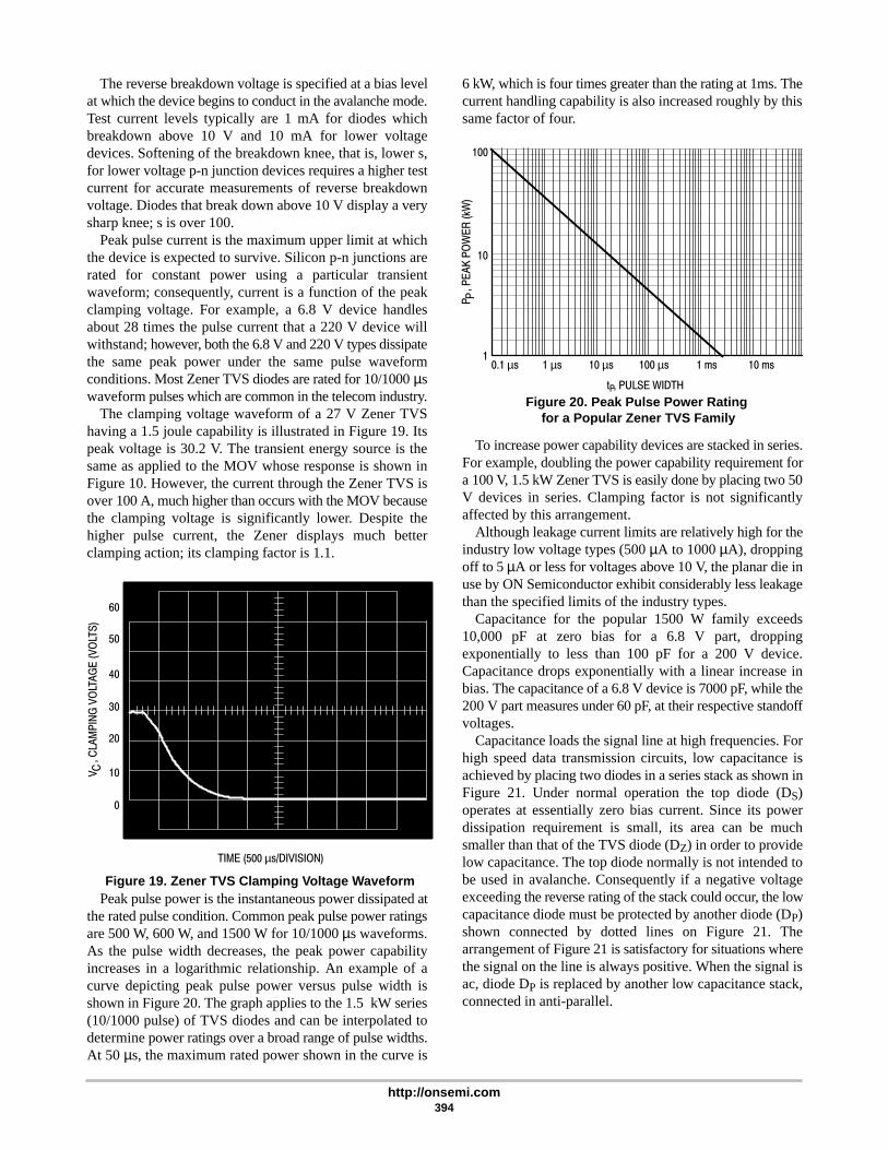
http://onsemi.com394
The reverse breakdown voltage is specified at a bias levelat which the device begins to conduct in the avalanche mode.Test current levels typically are 1 mA for diodes whichbreakdown above 10 V and 10 mA for lower voltagedevices. Softening of the breakdown knee, that is, lower s,for lower voltage p-n junction devices requires a higher testcurrent for accurate measurements of reverse breakdownvoltage. Diodes that break down above 10 V display a verysharp knee; s is over 100.
Peak pulse current is the maximum upper limit at whichthe device is expected to survive. Silicon p-n junctions arerated for constant power using a particular transientwaveform; consequently, current is a function of the peakclamping voltage. For example, a 6.8 V device handlesabout 28 times the pulse current that a 220 V device willwithstand; however, both the 6.8 V and 220 V types dissipatethe same peak power under the same pulse waveformconditions. Most Zener TVS diodes are rated for 10/1000 µswaveform pulses which are common in the telecom industry.
The clamping voltage waveform of a 27 V Zener TVShaving a 1.5 joule capability is illustrated in Figure 19. Itspeak voltage is 30.2 V. The transient energy source is thesame as applied to the MOV whose response is shown inFigure 10. However, the current through the Zener TVS isover 100 A, much higher than occurs with the MOV becausethe clamping voltage is significantly lower. Despite thehigher pulse current, the Zener displays much betterclamping action; its clamping factor is 1.1.
Figure 14
Figure 19. Zener TVS Clamping Voltage Waveform
TIME (500 µs/DIVISION)
0
10
20
30
40
50
60
V
, CLA
MP
ING
VO
LTA
GE
(V
OLT
S)
C
Peak pulse power is the instantaneous power dissipated atthe rated pulse condition. Common peak pulse power ratingsare 500 W, 600 W, and 1500 W for 10/1000 µs waveforms.As the pulse width decreases, the peak power capabilityincreases in a logarithmic relationship. An example of acurve depicting peak pulse power versus pulse width isshown in Figure 20. The graph applies to the 1.5 kW series(10/1000 pulse) of TVS diodes and can be interpolated todetermine power ratings over a broad range of pulse widths.At 50 µs, the maximum rated power shown in the curve is
6 kW, which is four times greater than the rating at 1ms. Thecurrent handling capability is also increased roughly by thissame factor of four.
Figure 20. Peak Pulse Power Rating for a Popular Zener TVS Family
1µs 10µs 100µs 1 ms 10 ms
100
10
1
tP, PULSE WIDTH
P P, P
EA
K P
OW
ER
(kW
)
0.1µs
To increase power capability devices are stacked in series.For example, doubling the power capability requirement fora 100 V, 1.5 kW Zener TVS is easily done by placing two 50V devices in series. Clamping factor is not significantlyaffected by this arrangement.
Although leakage current limits are relatively high for theindustry low voltage types (500 µA to 1000 µA), droppingoff to 5 µA or less for voltages above 10 V, the planar die inuse by ON Semiconductor exhibit considerably less leakagethan the specified limits of the industry types.
Capacitance for the popular 1500 W family exceeds10,000 pF at zero bias for a 6.8 V part, droppingexponentially to less than 100 pF for a 200 V device.Capacitance drops exponentially with a linear increase inbias. The capacitance of a 6.8 V device is 7000 pF, while the200 V part measures under 60 pF, at their respective standoffvoltages.
Capacitance loads the signal line at high frequencies. Forhigh speed data transmission circuits, low capacitance isachieved by placing two diodes in a series stack as shown inFigure 21. Under normal operation the top diode (DS)operates at essentially zero bias current. Since its powerdissipation requirement is small, its area can be muchsmaller than that of the TVS diode (DZ) in order to providelow capacitance. The top diode normally is not intended tobe used in avalanche. Consequently if a negative voltageexceeding the reverse rating of the stack could occur, the lowcapacitance diode must be protected by another diode (DP)shown connected by dotted lines on Figure 21. Thearrangement of Figure 21 is satisfactory for situations wherethe signal on the line is always positive. When the signal isac, diode DP is replaced by another low capacitance stack,connected in anti-parallel.
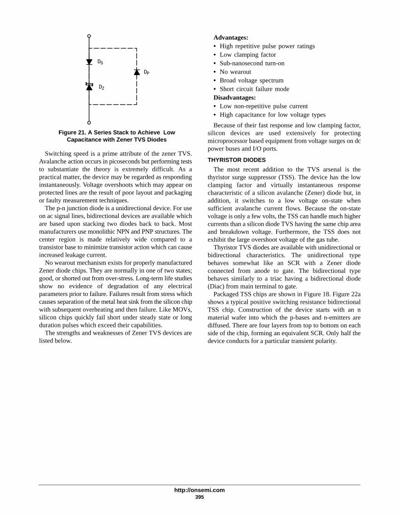
http://onsemi.com395
DS
DZ
DP
Figure 21. A Series Stack to Achieve LowCapacitance with Zener TVS Diodes
Switching speed is a prime attribute of the zener TVS.Avalanche action occurs in picoseconds but performing teststo substantiate the theory is extremely difficult. As apractical matter, the device may be regarded as respondinginstantaneously. Voltage overshoots which may appear onprotected lines are the result of poor layout and packagingor faulty measurement techniques.
The p-n junction diode is a unidirectional device. For useon ac signal lines, bidirectional devices are available whichare based upon stacking two diodes back to back. Mostmanufacturers use monolithic NPN and PNP structures. Thecenter region is made relatively wide compared to atransistor base to minimize transistor action which can causeincreased leakage current.
No wearout mechanism exists for properly manufacturedZener diode chips. They are normally in one of two states;good, or shorted out from over-stress. Long-term life studiesshow no evidence of degradation of any electricalparameters prior to failure. Failures result from stress whichcauses separation of the metal heat sink from the silicon chipwith subsequent overheating and then failure. Like MOVs,silicon chips quickly fail short under steady state or longduration pulses which exceed their capabilities.
The strengths and weaknesses of Zener TVS devices arelisted below.
Advantages:• High repetitive pulse power ratings• Low clamping factor• Sub-nanosecond turn-on• No wearout• Broad voltage spectrum• Short circuit failure modeDisadvantages:• Low non-repetitive pulse current• High capacitance for low voltage types
Because of their fast response and low clamping factor,silicon devices are used extensively for protectingmicroprocessor based equipment from voltage surges on dcpower buses and I/O ports.
THYRISTOR DIODES
The most recent addition to the TVS arsenal is thethyristor surge suppressor (TSS). The device has the lowclamping factor and virtually instantaneous responsecharacteristic of a silicon avalanche (Zener) diode but, inaddition, it switches to a low voltage on-state whensufficient avalanche current flows. Because the on-statevoltage is only a few volts, the TSS can handle much highercurrents than a silicon diode TVS having the same chip areaand breakdown voltage. Furthermore, the TSS does notexhibit the large overshoot voltage of the gas tube.
Thyristor TVS diodes are available with unidirectional orbidirectional characteristics. The unidirectional typebehaves somewhat like an SCR with a Zener diodeconnected from anode to gate. The bidirectional typebehaves similarly to a triac having a bidirectional diode(Diac) from main terminal to gate.
Packaged TSS chips are shown in Figure 18. Figure 22ashows a typical positive switching resistance bidirectionalTSS chip. Construction of the device starts with an nmaterial wafer into which the p-bases and n-emitters arediffused. There are four layers from top to bottom on eachside of the chip, forming an equivalent SCR. Only half thedevice conducts for a particular transient polarity.

http://onsemi.com396
Figure 22a. Chip Construction
ÈÈÈÈÈÈÈÈ
ÈÈÈÈÈÈÈÈ
A
K
Figure 22c. Circuit Modelof Left Side
A
K
P EMITTER
N BASE
N E
MIT
TE
R
P B
AS
E
Figure 22b. Cross Sectionof Left Side
MT1 MT2
Figure 22d. Circuit Symbol
The “gate” does not trigger the SCR, instead, operation inthe Zener mode begins when the collector junctionavalanches. Note that the p-bases pass through then-emitters in a dot pattern and connect to the contact metalcovering both halves of the chip. This constructiontechnique provides a low resistance path for current flowand prevents it from turning on the NPN transistor.Therefore, at relatively low currents, the device acts like alow gain PNP transistor in breakdown. The Zener diode isthe collector base junction of the PNP transistor. Negativeresistance TSS devices are similarly constructed but startwith p-type material wafer, allowing the fabrication of ahigh-gain NPN transistor. The switchback in voltage withincreasing current is caused by the gain of the NPN.
Both device types switch on completely when the currentflow through the base emitter shunt resistance causesenough voltage drop to turn on the emitter and begin fourlayer action. Now the device acts like an SCR. The collectorcurrent of the PNP transistor (Figure 22c) provides the basedrive for the NPN transistor. Likewise, the collector current
of the NPN transistor drives the base of the PNP causing thetwo devices to hold one another on. Both the p and n emittersflood the chip with carriers resulting in high electricalconductivity and surge current capability.
When driven with high voltage ac, which occurs during apower cross, positive resistance TSS devices act like a Zenerdiode until the ac voltage drives the load line through thepoint where regeneration occurs. Then it abruptly switchesto a low voltage. When the peak ac current is just below thecurrent required for breakover, the device operates mainlyas a Zener and power dissipation is high although the currentis low. When the ac current peak is well above breakover,(>10 A), the device operates mainly as an SCR, and the lowon-state voltage causes power dissipation to be relativelylow.
Negative resistance devices operate in a similar fashion.However, their behavior is dependent upon the “load line,”that is, the equivalent resistance which the device “sees.”When the load resistance is high (>1000 W) behavior issimilar to that of a positive resistance TSS in that high

http://onsemi.com397
instantaneous power dissipation occurs as the load line isdriven along the high voltage region of the TSS prior toswitching.
When a TSS with a negative resistance characteristic isdriven with a low “load” resistance, switching occurs whenthe load line is tangent to the peak of the negative resistancecurve. Thus, complete turn-on can occur at a very lowcurrent if the load resistance is low and the device has a“sharp” switchback characteristic.
Leakage and the Zener knee voltage increase withtemperature at eight percent and 0.11% per °C respectivelyfor 200 V positive resistance types. But the current requiredto cause regeneration falls with temperature, causing lessZener impedance contribution to the breakover voltage,resulting in a large reduction in the breakover voltagetemperature coefficient to as little as 0.05%/°C. Negativeresistance types can show positive or negative breakovervoltage coefficients depending on temperature and thesharpness of the negative switchback.
The response of both positive and negative switchingresistance units to fast transients involves a race betweentheir Zener and regenerative attributes. At first the deviceconducts only in the small chip area where breakdown isoccurring. Time is required for conduction to spread acrossthe chip and to establish the currents and temperaturesleading to complete turn-on. The net result is that both typesexhibit increasing breakover voltage with fast transients.However, this effect is very small compared to gas dischargetubes, being less than 25% of the breakover voltage.
Negative resistance types are more sensitive to unwantedturn-on by voltage rates (dv/dt) at peak voltages below theavalanche value. The transient current that flows to chargethe self-capacitance of the device sets up an operating pointon the negative resistance slope leading to turn-on.Reduction of dv/dt capability becomes significant when thesignal voltage exceeds 80% of the avalanche value.
Complete turn-off following a transient requires the loadline to intersect the device leakage characteristic at a pointbelow the avalanche knee. During turn-off the load line mustnot meet an intermediate conducting state which can occurwith a negative resistance device. Positive resistance typesare free of states causing turn-off “sticking.” Both typeshave temperature sensitive holding currents that lie between1 and 4 mA/°C.
Recent product developments and published studies havegenerated much interest. Based on a study sponsored by BellSouth,9 the authors concluded that these new devices offeredthe highest level of surge protection available.
Key electrical parameters for the Thyristor TVS includeoperating voltage, clamping voltage, pulse current, on-statevoltage, capacitance, and holding current.
Operating voltage is defined as the maximum normalvoltage which the device should experience. Operatingvoltages from 60 V to 200 V are available.
Clamping voltage is the maximum voltage level attainedbefore thyristor turn-on and subsequent transition to the
on-state conduction mode. The transition stage toconduction may have any of the slopes shown in Figure 9.
The important voltages which define the thyristoroperating characteristics are also shown in Figure 9. VD isoperating voltage, VC is the clamping voltage and VT ison-state voltage.
On-state voltage for most devices is approximately 3 V.Consequently, transient power dissipation is much lower forthe thyristor TVS than for other TVS devices because of itslow on-state voltage. For example, under power crossconditions Bell South Services reported their tests showedthat the thyristor TVS devices handled short bursts ofcommercial power with far less heating than arc type surgearrestors.9
Capacitance is also a key parameter since in many casesthe TSS is a replacement for gas surge arrestors which havelow capacitance. Values for the TSS range from 100 pF to200 pF at zero volts, but drop to about half of these valuesat a 50 Vdc bias.
Holding current (IH) is defined as the current required tomaintain the on-state condition. Device thru-current mustdrop below IH before it will restore to the non-conductingstate. Turn-off time is usually not specified but it can beexpected to be several milliseconds in a telecom applicationwhere the dc follow-on current is just slightly below theholding current.
The major advantages and limitations of the thyristor are:
Advantages:• Fast response• No wearout• Produces no noise• Short circuit failure modeDisadvantages:• Narrow voltage spectrum• Non-restoring in dc circuits unless current is below IH
• Turn-off delay time
The thyristor TVS is finding wide acceptance in telecomapplications because its characteristics uniquely matchtelecom requirements. It handles the difficult “power cross”requirements with less stress than other TVS devices whileproviding the total protection needed.
SURGE PROTECTOR MODULESTYPES OF SURGE PROTECTOR MODULES
Several component technologies have been implementedeither singly or in combination in surge protector modulesand devices. The simplest surge protectors contain nothingmore than a single transient voltage suppression (TVS)component in a larger package. Others contain two or morein a series, parallel or series-parallel arrangement. Stillothers contain two or more varieties of TVS elements incombination, providing multiple levels of protection.
Many surge protectors contain non-semiconductorelements such as carbon blocks and varistors. If required,
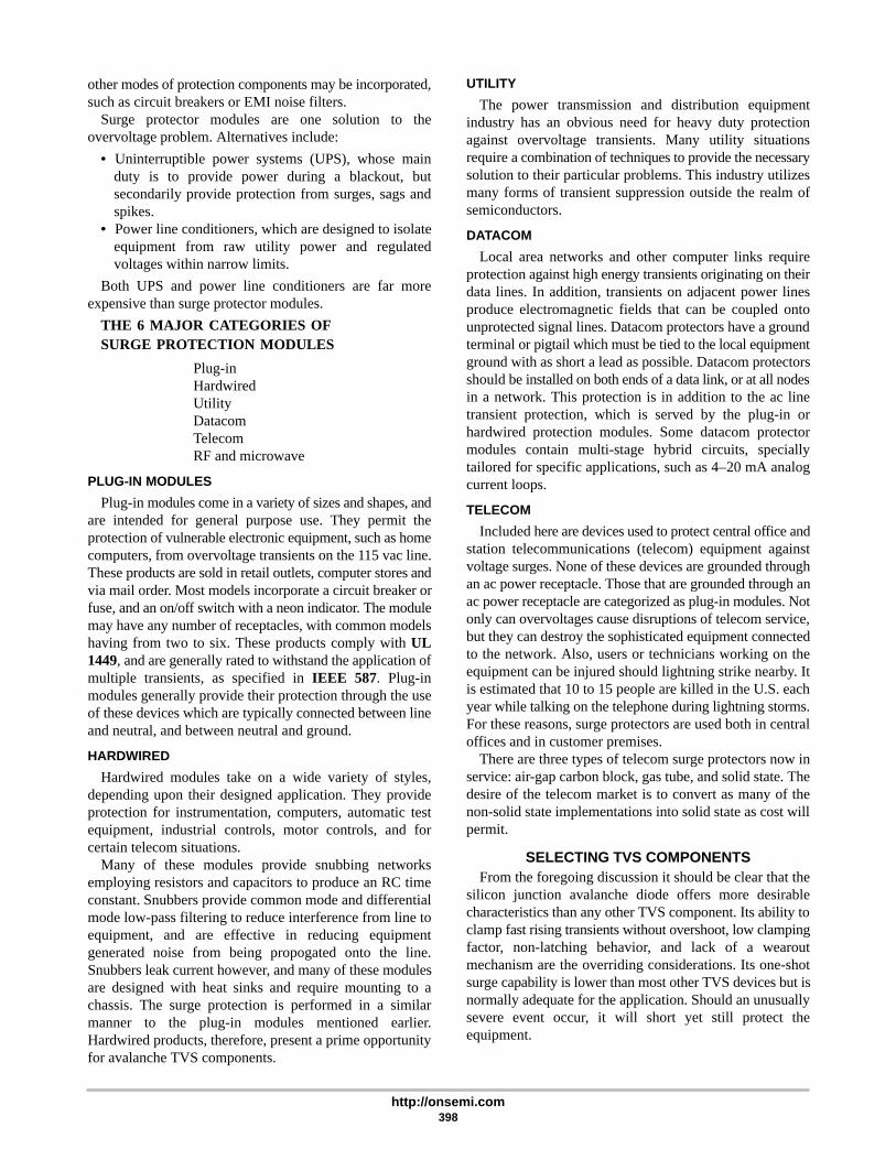
http://onsemi.com398
other modes of protection components may be incorporated,such as circuit breakers or EMI noise filters.
Surge protector modules are one solution to theovervoltage problem. Alternatives include:
• Uninterruptible power systems (UPS), whose mainduty is to provide power during a blackout, butsecondarily provide protection from surges, sags andspikes.
• Power line conditioners, which are designed to isolateequipment from raw utility power and regulatedvoltages within narrow limits.
Both UPS and power line conditioners are far moreexpensive than surge protector modules.
THE 6 MAJOR CATEGORIES OFSURGE PROTECTION MODULES
Plug-inHardwiredUtilityDatacomTelecomRF and microwave
PLUG-IN MODULES
Plug-in modules come in a variety of sizes and shapes, andare intended for general purpose use. They permit theprotection of vulnerable electronic equipment, such as homecomputers, from overvoltage transients on the 115 vac line.These products are sold in retail outlets, computer stores andvia mail order. Most models incorporate a circuit breaker orfuse, and an on/off switch with a neon indicator. The modulemay have any number of receptacles, with common modelshaving from two to six. These products comply with UL1449, and are generally rated to withstand the application ofmultiple transients, as specified in IEEE 587. Plug-inmodules generally provide their protection through the useof these devices which are typically connected between lineand neutral, and between neutral and ground.
HARDWIRED
Hardwired modules take on a wide variety of styles,depending upon their designed application. They provideprotection for instrumentation, computers, automatic testequipment, industrial controls, motor controls, and forcertain telecom situations.
Many of these modules provide snubbing networksemploying resistors and capacitors to produce an RC timeconstant. Snubbers provide common mode and differentialmode low-pass filtering to reduce interference from line toequipment, and are effective in reducing equipmentgenerated noise from being propogated onto the line.Snubbers leak current however, and many of these modulesare designed with heat sinks and require mounting to achassis. The surge protection is performed in a similarmanner to the plug-in modules mentioned earlier.Hardwired products, therefore, present a prime opportunityfor avalanche TVS components.
UTILITY
The power transmission and distribution equipmentindustry has an obvious need for heavy duty protectionagainst overvoltage transients. Many utility situationsrequire a combination of techniques to provide the necessarysolution to their particular problems. This industry utilizesmany forms of transient suppression outside the realm ofsemiconductors.
DATACOM
Local area networks and other computer links requireprotection against high energy transients originating on theirdata lines. In addition, transients on adjacent power linesproduce electromagnetic fields that can be coupled ontounprotected signal lines. Datacom protectors have a groundterminal or pigtail which must be tied to the local equipmentground with as short a lead as possible. Datacom protectorsshould be installed on both ends of a data link, or at all nodesin a network. This protection is in addition to the ac linetransient protection, which is served by the plug-in orhardwired protection modules. Some datacom protectormodules contain multi-stage hybrid circuits, speciallytailored for specific applications, such as 4–20 mA analogcurrent loops.
TELECOM
Included here are devices used to protect central office andstation telecommunications (telecom) equipment againstvoltage surges. None of these devices are grounded throughan ac power receptacle. Those that are grounded through anac power receptacle are categorized as plug-in modules. Notonly can overvoltages cause disruptions of telecom service,but they can destroy the sophisticated equipment connectedto the network. Also, users or technicians working on theequipment can be injured should lightning strike nearby. Itis estimated that 10 to 15 people are killed in the U.S. eachyear while talking on the telephone during lightning storms.For these reasons, surge protectors are used both in centraloffices and in customer premises.
There are three types of telecom surge protectors now inservice: air-gap carbon block, gas tube, and solid state. Thedesire of the telecom market is to convert as many of thenon-solid state implementations into solid state as cost willpermit.
SELECTING TVS COMPONENTSFrom the foregoing discussion it should be clear that the
silicon junction avalanche diode offers more desirablecharacteristics than any other TVS component. Its ability toclamp fast rising transients without overshoot, low clampingfactor, non-latching behavior, and lack of a wearoutmechanism are the overriding considerations. Its one-shotsurge capability is lower than most other TVS devices but isnormally adequate for the application. Should an unusuallysevere event occur, it will short yet still protect theequipment.

http://onsemi.com399
For example, an RS-232 data line is specified to operatewith a maximum signal level of ± 25 V. Failure analysisstudies11 have shown that the transmitters and receiversused on RS-232 links tolerate 40 V transients. A1.5KE27CA diode will handle the maximum signal levelwhile holding the peak transient voltage to less than 40 Vwith a 40 A 10/1000 pulse which is adequate for all indoorand most outdoor data line runs. As a practical matter, fewdata links use 25 V signals; 5 V is most common.Consequently, much lower voltage silicon diodes may beused which will allow a corresponding increase in surgecurrent capability. For example, a 10 V breakdown devicefrom the same 1500 W family will clamp to under 15 V(typically 12 V) when subjected to a 100 A pulse.
Telecommunications lines which must accommodate thering voltage have much more severe requirements. Forexample, one specification11 from Bellcore suggests thatleakage current be under 20 mA over the temperature rangefrom –40°C to +65°C with 265 V peak ac applied. To meetthis specification using Zener TVS parts, devices must bestacked. Devices which breakdown at 160 V are chosen toaccommodate tolerances and the temperature coefficient. Apart number with a 10% tolerance on breakdown couldsupply a unit which breaks down at 144 V. At –40°Cbreakdown could be 133 V. The breakdown of two devicesstacked just barely exceeds the worst case ring peak of265 V. A 1500 W unit has a surge capability of 6.5 A(10/1000) which is too low to be satisfactory while higherpower units are too expensive as a rule.
Another problem which telephone line service presents toa surge suppressor is survival during a power cross. Anavalanche diode is impractical to use because the energydelivered by a power cross will produce diode failure beforeany overcurrent protective element can react.
As indicated by the Bell South studies, the thyristor TVSis ideal for telephone line applications. Suppliers offerunidirectional and bidirectional units which meet the FCCimpulse wave requirements as shown in Table 1. In addition,the thyristor can handle several cycles of 50/60 Hz powerbefore failure. The ON Semiconductor MKT1V200 series,for example, can handle 10 A for 4 cycles, which is enoughtime for a low current fuse or other current activatedprotective device to react.
APPLICATION CONSIDERATIONSIn most cases, it is not advisable to place a zener TVS
directly across a data line because of its relatively highcapacitance. The arrangement previously discussed andshown in Figure 21 works well for an unbalanced line suchas RS-232. When using discrete steering diodes, they shouldhave low capacitance and low turn-on impedance to avoidcausing an overshoot on the clamped voltage level.
Most noise and transient surge voltages occur on lineswith respect to ground. A signal line such as RS-232 whichuses ground as a signal reference is thus very vulnerable tonoise and transients. It is, however, easy to protect using asingle TVS at each end of the line.
Telephone and RS-422 lines are called balanced linesbecause the signal is placed between two lines which are“floating” with respect to ground. A signal appears betweeneach signal line and ground but is rejected by the receiver;only the difference in potential between the two signal linesis recognized as the transmitted signal. This system has beenin use for decades as a means of providing improved noiseimmunity, but protection from transient surge voltages ismore complex.
A cost-effective means of protecting a balanced line isshown in Figure 23. The bridge diode arrangement allowsprotection against both positive and negative transients to beachieved, an essential requirement but the TVS devices Z1and Z2 need only be unidirectional. The diodes are chosento have low capacitance to reduce loading on the line andlow turn-on impedance to avoid causing an overshoot on theclamped voltage level. Although a zener TVS is shown, aTSS is more appropriate when a telephone line having ringvoltages is to be protected.
D2D1
D3 D4
Z2Z1
Figure 23. A Method of Reducing Capacitance andProtecting a Balanced Line
Since transients are usually common-mode, it is importantthat the TVS circuit operate in a balanced fashion;otherwise, common mode transients can cause differentialmode disturbances which can be devastating to the linereceiver. For example, suppose that an identical positivecommon mode surge voltage appears from eachline-to-ground. Diodes D2 and D4 will conduct the transientsto Z2. However, if one of these diodes has a slower turn-onor higher dynamic impedance than the other, the voltagedifference caused by the differing diode response appearsacross the signal lines. Consequently, the bridge diodes mustbe chosen to be as nearly identical as possible.
Should a differential mode transient appear on the signallines, it will be held to twice that of the line-to-groundclamping level. In many cases a lower clamping level isneeded which can be achieved by placing another TVSacross the signal lines. It must be a bidirectional low

http://onsemi.com400
capacitance device. With a line-to-line TVS in the circuitdiode matching is not required.
Other schemes appearing in the literature use twobidirectional TVS devices from each line-to-ground asshown in Figure 24 that of the line-to-ground voltage. Toavoid generating a differential mode signal, the TVS mustbe closely matched or a third TVS must be placedline-to-line. By using a third TVS differential modetransients can be held to a low level.
T3
TIP
RING
T1
T2
Figure 24. Protecting a Balanced Line withBidirectional TSS Devices
The arrangement of Figure 25 offers the advantage oflower capacitance when differential mode transientprotection is required. If all three TSS devices have the samecapacitance (C), the line-to-line and line-to-groundcapacitance of Figure 24 is 1.5C. However, the arrangementof Figure 25 exhibits a capacitance of only C/2. To design thecircuit to handle the same simultaneous common modeenergy as the circuit of Figure 24, T3 must be twice as largeas T1 and T2. In this case the capacitance of T3 is doubledwhich causes the line-to-ground capacitance to be 2C/3, stilla considerable improvement over the arrangement ofFigure 24.
T3
TIP
RING
T1
T2
Figure 25. Preferred Method of Protecting aBalanced Line Using Bidirectional TSS Devices
Protectors are usually designed to be “fail safe” if theirenergy ratings are exceeded, but the definition of “fail safe”is often dependent upon the application. The most commonrequirement is that the surge voltage protective elementshould fail short and remain shorted regardless of the
resulting current flow. To insure that this occurs,semiconductor devices use heavy gauge clips or bondingwires between the chip and terminals. In addition, parts areavailable in plastic packages having a spring type shortingbar which shorts the terminals when the package softens atthe very high temperatures generated during a severeoverload.
The shorted TVS protects the equipment, but the linefeeding it could be destroyed if the source of energy whichshorted the TVS is from a power cross. Therefore, it is wiseand necessary for a UL listing to provide a series elementsuch as a fuse or PTC device to either open the circuit orrestrict its value to a safe level.
The design of circuit boards is critical and layout must bedone to minimize any lead or wiring inductance in serieswith the TVS. Significant voltage is developed in any loopsubject to transients because of their high current amplitudesand fast risetimes.
REFERENCES1. D. W. Bodle and P. A. Gresh, “Lightning Surges in
Paired Telephone Cable Facilities,” The Bell SystemTechnical Journal, Vol. 4, March 1961, pp. 547–576.
2. D. G. Stroh, “Static Electricity Can Kill Transistors,”Electronics, Vol. 35, 1962, pp. 90–91.
3. J. D. Norgard and C. L. Chen, “Lightning-InducedTransients on Buried Shielded Transmission Lines,”IEEE Transactions on EMC, Vol. EMC28, No. 3,August 1986, pp. 168–171.
4. O. M. Clark, “Transient Voltage Suppression (TVS),”1989, pp. 6–7.
5. Clark, p. 7.6. World Information Technologies, “U. S. Electrical and
Electronic Surge Protection Markets,” 1989, p. 5.7. T. J. Tucker, “Spark Initiation Requirements of a
Secondary Explosive,” Annals of the New YorkAcademy of Sciences, Vol. 152, Article I, 1968, pp.643–653.
8. H. K. Florig, “The Future Battlefield: A Blast ofGigawatts?,” IEEE Spectrum, Vol. 25, No. 3, March1988, pp. 50–54.
9. Mel Thrasher, “A Solid State Solution,” Telephony,June 1989, pp. 48–52.
10. A. Urbieta, “Sensitivity Study to EOS/SSD of BipolarIntegrated Circuits,” EOS-8, 1986.
11. M. Tetreault and F.D. Martzloff, “Characterization ofDisturbing Transient Waveforms on Computer DataCommunication Lines,” EMC Proceedings, Zurich,March 1985, pp. 423–428.
12. F. Martzloff, “Coupling, Propagation, and Side Effectsof Surges in an Industrial Building Wiring System,”Conference Record of IEEE IAS Meeting, 1988, pp.1467–1475.

http://onsemi.com401
IMPORTANT REGULATORY REQUIREMENTSAND GUIDELINES
GENERAL
DOD-STD-1399, MIL-STD-704, MIL-STD-1275,MIL-STD-461C. These military specifications areimportant, if we intend to target devices for military orcommercial aviation markets.
IEEE 587. This specification describes multiple transientwaveforms.
UL1449. This is a compulsory test which demonstratesperformance to criteria establishing the maximum voltagethat can pass through a device after clamping has takenplace. It is important that we comply, and say so on our datasheets.
INDUSTRIAL
ANSI/IEEE C62.41. Established by the AmericanNational Standards Institute (ANSI) and the Institute ofElectrical and Electronic Engineers (IEEE), this guidelinetests the effectiveness of devices to typical powerdisturbances. To meet the most rigorous category of thisspec, a device or module must be capable of withstanding amaximum repetitive surge current pulse of 3000 amps witha 8/20 µs waveform.
IEC TC 102 D. Requirements for remote controlreceivers for industrial applications are detailed in thisInternational Electrotechnical Commission (IEC)document.
IEC 255-4 and IEC TC 41. These documents describetesting for static relays for industrial use.
IEC 801-1 thru -3. These are specifications for variousindustrial control applications.
IEC 801-4. The IEC specifies transient voltage impulseswhich occur from the switching of inductive loads. We mustbe aware of the importance of this specification, especiallyin Europe, and characterize our devices’ performance to it.
IEEE 472/ANSI C 37.90.1. Requirements for protectiverelays, including 10/1000 nS waveform testing is described.
UL943. This requirement defines a 0.5 µs/100 kHzwaveform for ground fault and other switching applications.
VDE 0420. Industrial remote control receivers aredetailed, and test procedures defined.
VDE 0860/Part 1/II. This includes a description of0.2/200 µs, 10kV test requirements.
TELECOM
CCITT IX K.17, K.20, K.15. These documents relate torepeaters.
EIA PM-1361. This document covers requirements fortelephone terminals and data processing equipment.
FTZ 4391 TV1. This is a general German specificationfor telecom equipment.
FCC Part 68. The Federal Communications Commission(FCC) requirements for communications equipment isdefined. Of special note is §68.302, dealing with telecompower lines.
NT/DAS/PRL/003. Telephone instrument, subscriberequipment and line requirements are documented.
PTT 692.01. This is a general Swiss specification fortelecom exchange equipment.
REA PE-60. The Rural Electrification Administration(REA) has documented the predominant waveform forinduced lightning transients. This test is now commonlyknown as the 10/1000 µs pulse test.
REA PE-80. The REA defines requirements for gas tubesand similar devices for telecom applications.
TA-TSY-000974. This technical advisory by Bellcoredefines double exponential waveforms, which are the basisfor many telecom applications norms.
UL 1459 and UL 4978. These document detail tests forstandard telephone equipment and data transmission.
TA-TSY-000974. This technical advisory by Bellcoredefines double exponential waveforms, which are the basisfor many telecom applications norms.
UL 1459 and UL 4978. These document detail tests forstandard telephone equipment and data transmission.

Semiconductor Components Industries, LLC, 2001
March, 2001 – Rev.0402 Publication Order Number:
AN784/D
AN784/D
Transient Power Capabilityof Zener Diodes
Prepared byApplications Engineering andJerry Wilhardt, Product Engineer — Industrial and Hi-Rel Zener Diodes
INTRODUCTIONBecause of the sensitivity of semiconductor components
to voltage transients in excess of their ratings, circuits areoften designed to inhibit voltage surges in order to protectequipment from catastrophic failure. External voltagetransients are imposed on power lines as a result of lightningstrikes, motors, solenoids, relays or SCR switching circuits,which share the same ac source with other equipment.Internal transients can be generated within a piece ofequipment by rectifier reverse recovery transients,switching of loads or transformer primaries, fuse blowing,solenoids, etc. The basic relation, v = L di/dt, describes mostequipment developed transients.
ZENER DIODE CHARACTERISTICSZener diodes, being nearly ideal clippers (that is, they
exhibit close to an infinite impedance below the clippinglevel and close to a short circuit above the clipping level), areoften used to suppress transients. In this type of application,it is important to know the power capability of the zener forshort pulse durations, since they are intolerant of excessivestress.
Some ON Semiconductor data sheets such as the ones fordevices shown in Table 1 contain short pulse surgecapability. However, there are many data sheets that do notcontain this data and Figure 1 is presented here tosupplement this information.
Table 1. Transient Suppressor Diodes
SeriesNumbers
SteadyState Power Package Description
1N4728 1 W DO-41 Double Slug Glass
1N6267 5 W Case 41A Axial Lead Plastic
1N5333A 5 W Case 17 Surmetic 40
1N746/957A/4371
400 mW DO-35 Double Slug Glass
1N5221A 500 mW DO-35 Double Slug Glass
Some data sheets have surge information which differsslightly from the data shown in Figure 1. A variety of reasonsexist for this:
1. The surge data may be presented in terms of actual surgepower instead of nominal power.
2. Product improvements have occurred since the datasheet was published.
Figure 1. Peak Power Ratings of Zener Diodes
Power is defined as VZ(NOM) x IZ(PK) where VZ(NOM) is the nominalzener voltage measured at the low test current used for voltageclassification.
1N6267 SERIES
GLASS DO35 & GLASS DO41250 mW TO 1 W TYPES
5 WATT TYPES
PULSE WIDTH (ms)
0.1
100
0.01 0.02
PP
K(N
OM
), N
OM
INA
L P
EA
K P
OW
ER
(kW
) 50
20
10
5
2
1
0.5
0.2
0.1
0.05
0.020.01
0.05 0.2 0.5 1 2 5 10
1 TO 3 W TYPESPLASTIC DO41
3. Larger dice are used, or special tests are imposed on theproduct to guarantee higher ratings than those shown onFigure 1.
4. The specifications may be based on a JEDECregistration or part number of another manufacturer.
The data of Figure 1 applies for non-repetitive conditionsand at a lead temperature of 25°C. If the duty cycle increases,the peak power must be reduced as indicated by the curvesof Figure 2. Average power must be derated as the lead orambient temperature rises above 25°C. The average powerderating curve normally given on data sheets may benormalized and used for this purpose.
At first glance the derating curves of Figure 2 appear to bein error as the 10 ms pulse has a higher derating factor thanthe 10 µs pulse. However, when the derating factor for agiven pulse of Figure 2 is multiplied by the peak power valueof Figure 1 for the same pulse, the results follow theexpected trend.
http://onsemi.com
APPLICATION NOTE
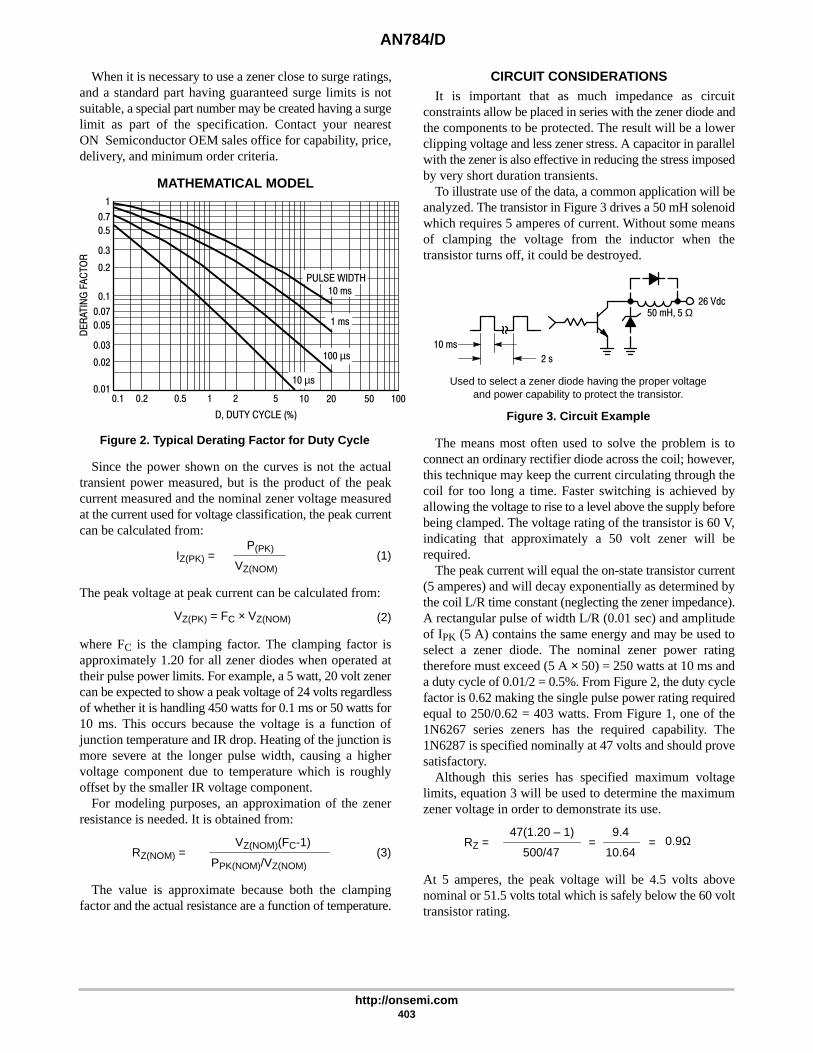
AN784/D
http://onsemi.com403
When it is necessary to use a zener close to surge ratings,and a standard part having guaranteed surge limits is notsuitable, a special part number may be created having a surgelimit as part of the specification. Contact your nearestON Semiconductor OEM sales office for capability, price,delivery, and minimum order criteria.
MATHEMATICAL MODEL
Figure 2. Typical Derating Factor for Duty Cycle
0.1
1
0.7
0.5
0.3
0.2
0.02
0.1
0.07
0.05
0.03
0.010.2 0.5 1 52 10 20 50 100
PULSE WIDTH10 ms
1 ms
100 µs
10 µs
D, DUTY CYCLE (%)
DE
RAT
ING
FA
CT
OR
Since the power shown on the curves is not the actualtransient power measured, but is the product of the peakcurrent measured and the nominal zener voltage measuredat the current used for voltage classification, the peak currentcan be calculated from:
IZ(PK) =P(PK)
VZ(NOM)(1)
The peak voltage at peak current can be calculated from:
(2)VZ(PK) = FC × VZ(NOM)
where FC is the clamping factor. The clamping factor isapproximately 1.20 for all zener diodes when operated attheir pulse power limits. For example, a 5 watt, 20 volt zenercan be expected to show a peak voltage of 24 volts regardlessof whether it is handling 450 watts for 0.1 ms or 50 watts for10 ms. This occurs because the voltage is a function ofjunction temperature and IR drop. Heating of the junction ismore severe at the longer pulse width, causing a highervoltage component due to temperature which is roughlyoffset by the smaller IR voltage component.
For modeling purposes, an approximation of the zenerresistance is needed. It is obtained from:
RZ(NOM) =VZ(NOM)(FC-1)
PPK(NOM)/VZ(NOM)(3)
The value is approximate because both the clampingfactor and the actual resistance are a function of temperature.
CIRCUIT CONSIDERATIONSIt is important that as much impedance as circuit
constraints allow be placed in series with the zener diode andthe components to be protected. The result will be a lowerclipping voltage and less zener stress. A capacitor in parallelwith the zener is also effective in reducing the stress imposedby very short duration transients.
To illustrate use of the data, a common application will beanalyzed. The transistor in Figure 3 drives a 50 mH solenoidwhich requires 5 amperes of current. Without some meansof clamping the voltage from the inductor when thetransistor turns off, it could be destroyed.
Figure 3. Circuit Example
Used to select a zener diode having the proper voltageand power capability to protect the transistor.
10 ms
2 s
26 Vdc50 mH, 5 Ω
The means most often used to solve the problem is toconnect an ordinary rectifier diode across the coil; however,this technique may keep the current circulating through thecoil for too long a time. Faster switching is achieved byallowing the voltage to rise to a level above the supply beforebeing clamped. The voltage rating of the transistor is 60 V,indicating that approximately a 50 volt zener will berequired.
The peak current will equal the on-state transistor current(5 amperes) and will decay exponentially as determined bythe coil L/R time constant (neglecting the zener impedance).A rectangular pulse of width L/R (0.01 sec) and amplitudeof IPK (5 A) contains the same energy and may be used toselect a zener diode. The nominal zener power ratingtherefore must exceed (5 A × 50) = 250 watts at 10 ms anda duty cycle of 0.01/2 = 0.5%. From Figure 2, the duty cyclefactor is 0.62 making the single pulse power rating requiredequal to 250/0.62 = 403 watts. From Figure 1, one of the1N6267 series zeners has the required capability. The1N6287 is specified nominally at 47 volts and should provesatisfactory.
Although this series has specified maximum voltagelimits, equation 3 will be used to determine the maximumzener voltage in order to demonstrate its use.
RZ =47(1.20 – 1)
500/47
9.4
10.64= = 0.9Ω
At 5 amperes, the peak voltage will be 4.5 volts abovenominal or 51.5 volts total which is safely below the 60 volttransistor rating.

Semiconductor Components Industries, LLC, 2001
March, 2001 – Rev.0404 Publication Order Number:
AN843/D
AN843/D
A Review of Transients andTheir Means of Suppression
Prepared bySteve CherniakApplications Engineering
INTRODUCTIONOne problem that most, if not all electronic equipment
designers must deal with, is transient overvoltages.Transients in electrical circuits result from the suddenrelease of previously stored energy. Some transients may bevoluntary and created in the circuit due to inductiveswitching, commutation voltage spikes, etc. and may beeasily suppressed since their energy content is known andpredictable. Other transients may be created outside thecircuit and then coupled into it. These can be caused bylightning, substation problems, or other such phenomena.These transients, unlike switching transients, are beyond thecontrol of the circuit designer and are more difficult toidentify, measure and suppress.
Effective transient suppression requires that the impulseenergy is dissipated in the added suppressor at a low enoughvoltage so the capabilities of the circuit or device will not beexceeded.
REOCCURRING TRANSIENTSTransients may be formed from energy stored in circuit
inductance and capacitance when electrical conditions in thecircuit are abruptly changed.
Switching induced transients are a good example of this;
the change in current didt in an inductor (L) will generate
a voltage equal to L didt. The energy (J) in the transient is equal
to 1/2Li2 and usually exists as a high power impulse for arelatively short time (J = Pt).
If load 2 is shorted (Figure 1), devices parallel to it maybe destroyed. When the fuse opens and interrupts the faultcurrent, the slightly inductive power supply produces a
transient voltage spike of V L didt with an energy content of
J = 1/2Li2. This transient might be beyond the voltagelimitations of the rectifiers and/or load 1. Switching out ahigh current load will have a similar effect.
TRANSFORMER PRIMARYBEING ENERGIZED
If a transformer is energized at the peak of the line voltage(Figure 2), this voltage step function can couple to the straycapacitance and inductance of the secondary winding andgenerate an oscillating transient voltage whose oscillationsdepend on circuit inductance and capacitance. Thistransient’s peak voltage can be up to twice the peakamplitude of the normal secondary voltage.
In addition to the above phenomena the capacitivelycoupled (CS) voltage spike has no direct relationship withthe turns ratio, so it is possible for the secondary circuit to seethe peak applied primary voltage.
Figure 1. Load Dump with Inductive Power Supply
POWER
SUPPLYA
BLOAD1
LOAD2
+
-
SHORTACROSSLOAD 2
FUSE
VAB
+
0
-
http://onsemi.com
APPLICATION NOTE

AN843/D
http://onsemi.com405
Figure 2. Situation Where Transformer Capacitance Causes a Transient
+
-
+
-
VLine
PEAK SHOULDBE 30% LIGHTER
CS
SWITCHCLOSEDVAB
VAB
LOADMAY HAVE STRAYINDUCTANCE ORCAPACITANCE
A
B
SWITCH
TRANSFORMER PRIMARYBEING DE-ENERGIZED
If the transformer is driving a high impedance load,transients of more than ten times normal voltage can becreated at the secondary when the primary circuit of thetransformer is opened during zero-voltage crossing of the acline. This is due to the interruption of the transformermagnetizing current which causes a rapid collapse of themagnetic flux in the core. This, in turn, causes a high voltagetransient to be coupled into the transformer’s secondarywinding (Figure 3).
Transients produced by interrupting transformersmagnetizing current can be severe. These transients candestroy a rectifier diode or filter capacitor if a lowimpedance discharge path is not provided.
SWITCH “ARCING”When a contact type switch opens and tries to interrupt
current in an inductive circuit, the inductance tries to keepcurrent flowing by charging stray capacitances. (SeeFigure 4.)
Figure 3. Typical Situation Showing Possible Transient When InterruptingTransformer Magnetizing Current
Figure 4. Transients Caused by Switch Opening
SWITCH
LOAD
AC
LINE
Im
SWITCH
OPENED
LINE
VOLTAGE
MAGNETIZING
CURRENT AND
FLUX
SECONDARY
VOLTAGE
VCap
VLine
TRANSIENT
SENSITIVE
LOAD
LINE
VOLTAGE

AN843/D
http://onsemi.com406
This can also happen when the switch contacts bounceopen after its initial closing. When the switch is opened (orbounces open momentarily) the current that the inductancewants to keep flowing will oscillate between the straycapacitance and the inductance. When the voltage due to theoscillation rises at the contacts, breakdown of the contactgap is possible, since the switch opens (or bounces open)relatively slowly compared to the oscillation frequency, andthe distance may be small enough to permit “arcing.” Thearc will discontinue at the zero current point of theoscillation, but as the oscillatory voltage builds up again andthe contacts move further apart, each arc will occur at ahigher voltage until the contacts are far enough apart tointerrupt the current.
WAVESHAPES OF SURGE VOLTAGESIndoor Waveshapes
Measurements in the field, laboratory, and theoreticalcalculations indicate that the majority of surge voltages inindoor low-voltage power systems have an oscillatorywaveshape. This is because the voltage surge excites thenatural resonant frequency of the indoor wiring system. Inaddition to being typically oscillatory, the surges can alsohave different amplitudes and waveshapes in the variousplaces of the wiring system. The resonant frequency canrange from about 5 kHz to over 500 kHz. A 100 kHzfrequency is a realistic value for a typical surge voltage formost residential and light industrial ac wire systems.
The waveshape shown in Figure 5 is known as an “0.5µs– 100 kHz ring wave.” This waveshape is reasonablyrepresentative of indoor low-voltage (120 V – 240 V) wiringsystem transients based on measurements conducted byseveral independent organizations. The waveshape isdefined as rising from 10% to 90% of its final amplitude in0.5 µs, then decays while oscillating at 100 kHz, each peakbeing 60% of the preceding one.
The fast rise portion of the waveform can induce theeffects associated with non-linear voltage distribution inwindings or cause dv/dt problems in semiconductors.Shorter rise times can be found in transients but they arelengthened as they propagate into the wiring system orreflected from wiring discontinuities.
Figure 5. 0.5 µs 100 kHz Ring Wave
0.9 Vpk
Vpk
t = 10 µs (f = 100 kHz)
0.1 Vpk
0.5 µs
60% OF Vpk
The oscillating portion of the waveform produces voltagepolarity reversal effects. Some semiconductors are sensitiveto polarity changes or can be damaged when forced into orout of conduction (i.e. reverse recovery of rectifier devices).The sensitivity of some semiconductors to the timing andpolarity of a surge is one of the reasons for selecting thisoscillatory waveform to represent actual conditions.
Outdoor Locations
Both oscillating and unidirectional transients have beenrecorded in outdoor environments (service entrances andother places nearby). In these locations substantial energy isstill available in the transient, so the waveform used tomodel transient conditions outside buildings must containgreater energy than one used to model indoor transientsurges.
Properly selected surge suppressors have a goodreputation of successful performance when chosen inconjunction with the waveforms described in Figure 6. Therecommended waveshape of 1.2 × 50 µs (1.2 µs is associatedwith the transients rise time and the 50 µs is the time it takesfor the voltage to drop to 1/2Vpk) for the open circuit voltageand 8 × 20 µs for the short circuit current are as defined inIEEE standard 28-ANSI Standard C62.1 and can beconsidered a realistic representation of an outdoor transientswaveshape.
Figure 6. Unidirectional Wave Shapes
V
0.9 Vpk
0.3 Vpk
0.1 Vpk
Vpk
0.5 Vpk
50 µs
t1 t1 × 1.67 = 1.2 µs
IIpk
0.9 Ipk
0.1 Ipk
0.5 Ipk
t220 µs
t2 × 1.25 = 8 µs
(a) Open-Circuit Voltage Waveform (b) Discharge Current Waveform

AN843/D
http://onsemi.com407
The type of device under test determines whichwaveshape in Figure 6 is more appropriate. The voltagewaveform is normally used for insulation voltage withstandtests and the current waveform is usually used for dischargecurrent tests.
RANDOM TRANSIENTSThe source powering the circuit or system is frequently
the cause of transient induced problems or failures. Thesetransients are difficult to deal with due to their nature; theyare totally random and it is difficult to define theiramplitude, duration and energy content. These transients aregenerally caused by switching parallel loads on the same
branch of a power distribution system and can also be causedby lightning.
AC POWER LINE TRANSIENTSTransients on the ac power line range from just above
normal voltage to several kV. The rate of occurrence oftransients varies widely from one branch of a powerdistribution system to the next, although low-level transientsoccur more often than high-level surges.
Data from surge counters and other sources is the basis forthe curves shown in Figure 7. This data was taken fromunprotected (no voltage limiting devices) circuits meaningthat the transient voltage is limited only by the sparkoverdistance of the wires in the distribution system.
Figure 7. Peak Surge Voltage versus Surges per Year*
*EIA paper, P587.1/F, May, 1979, Page 10
20
10
5
4
0.7
0.2
0.1
0.5
0.3
9
8
7
6
1
3
2
0.90.8
0.4
0.6
0.01 10.1 10 100 1000
SURGES PER YEAR
PEAK
SURGE
VOLTAGE
(kV)
HIGH EXPOSURE
MEDIUM EXPOSURE
LOW EXPOSURE

AN843/D
http://onsemi.com408
The low exposure portion of the set of curves is datacollected from systems with little load-switching activitythat are located in areas of light lightning activity.
Medium exposure systems are in areas of frequentlightning activity with a severe switching transient problem.
High exposure systems are rare systems supplied by longoverhead lines which supply installations that have highsparkover clearances and may be subject to reflections atpower line ends.
When using Figure 7 it is helpful to remember that peaktransient voltages will be limited to approximately 6 kV inindoor locations due to the spacing between conductorsusing standard wiring practices.
TRANSIENT ENERGY LEVELS ANDSOURCE IMPEDANCE
The energy contained in a transient will be divided betweenthe transient suppressor and the source impedance of thetransient in a way that is determined by the two impedances.With a spark-gap type suppressor, the low impedance of theArc after breakdown forces most of the transient’s energy tobe dissipated elsewhere, e.g. in a current limiting resistor inseries with the spark-gap and/or in the transient’s sourceimpedance. Voltage clamping suppressors (e.g. zeners,mov’s, rectifiers operating in the breakdown region) on theother hand absorb a large portion of the transient’s surgeenergy. So it is necessary that a realistic assumption of thetransient’s source impedance be made in order to be able toselect a device with an adequate surge capability.
The 100 kHz “Ring Wave” shown in Figure 5 is intendedto represent a transient’s waveshape across an open circuit.The waveshape will change when a load is connected and theamount of change will depend on the transient’s sourceimpedance. The surge suppressor must be able to withstandthe current passed through it from the surge source. Anassumption of too high a surge impedance (when testing thesuppressor) will not subject the device under test tosufficient stresses, while an assumption of too low a surgeimpedance may subject it to an unrealistically large stress;there is a trade-off between the size (cost) of the suppressorand the amount of protection obtained.
In a building, the transient’s source impedance increaseswith the distance from the electrical service entrance, but
open circuit voltages do not change very much throughoutthe structure since the wiring does not provide muchattenuation. There are three categories of service locationsthat can represent the majority of locations from theelectrical service entrance to the most remote wall outlet.These are listed below. Table 1 is intended as an aid for thepreliminary selection of surge suppression devices, since itis very difficult to select a specific value of sourceimpedance.
Category I: Outlets and circuits a “long distance” fromelectrical service entrance. Outlets more than 10 metersfrom Category II or more than 20 meters from CategoryIII (wire gauge #14 – #10)
Category II: Major bus lines and circuits a “short distance”from electrical service entrance. Bus system in industrialplants. Outlets for heavy duty appliances that are “close”to the service entrance.
Distribution panel devices.Commercial building lighting systems.
Category III. Electrical service entrance and outdoorlocations.
Power line between pole and electrical service entrance.Power line between distribution panel and meter.Power line connection to additional near-by buildings.Underground power lines leading to pumps, filters, etc.
Categories I and II in Table 1 correspond to the extremerange of the “medium exposure” curve in Figure 7. Thesurge voltage is limited to approximately 6 kV due to thesparkover spacing of indoor wiring.
The discharge currents of Category II were obtained fromsimulated lightning tests and field experience withsuppressor performance.
The surge currents in Category I are less than in CategoryII because of the increase in surge impedance due to the factthat Category I is further away from the service entrance.
Category III can be compared to the “High Exposure”situation in Figure 7. The limiting effect of sparkover is notavailable here so the transient voltage can be quite large.
Table 1. Surge Voltages and Currents Deemed to Represent the Indoor Environment Depending Upon LocationEnergy (Joules) Dissipated in a
Suppressor with a Clamping Voltage of (3)
Category Waveform Surge Voltage (1) Surge Current (2) 250 V 500 V 1000 V
I 0.5 µs 100 kHzRing Wave
6 kV 200 A 0.4 0.8 1.6
II 0.5 µs 100 kHzRing Wave
6 kV 500 A 1 2 4
1.2 × 50 µs8 × 20 µs
6 kV3 kA 20 40 80
III 1.2 × 50 µs8 × 20 µs
10 kV or more10 kA or more
Notes: 1. Open Circuit voltageNotes: 2. Discharge current of the surge (not the short circuit current of the power system)Notes: 3. The energy a suppressor will dissipate varies in proportion with the suppressor’s clamping voltage, which can be different with different system voltages (assuming the sameNotes: 3. discharge current).

AN843/D
http://onsemi.com409
LIGHTNING TRANSIENTSThere are several mechanisms in which lightning can
produce surge voltages on power distribution lines. One ofthem is a direct lightning strike to a primary (before thesubstation) circuit. When this high current, that is injectedinto the power line, flows through ground resistance and thesurge impedance of the conductors, very large transientvoltages will be produced. If the lightning misses theprimary power line but hits a nearby object the lightningdischarge may also induce large voltage transients on theline. When a primary circuit surge arrester operates andlimits the primary voltage the rapid dv/dt produced willeffectively couple transients to the secondary circuit throughthe capacitance of the transformer (substation) windings inaddition to those coupled into the secondary circuit bynormal transformer action. If lightning struck the secondarycircuit directly, very high currents may be involved whichwould exceed the capability of conventional surgesuppressors. Lightning ground current flow resulting fromnearby direct to ground discharges can couple onto thecommon ground impedance paths of the groundingnetworks also causing transients.
AUTOMOTIVE TRANSIENTSTransients in the automotive environment can range from
the noise generated by the ignition system and the variousaccessories (radio, power window, etc.) to the potentiallydestructive high energy transients caused by the charging(alternator/regulator) system. The automotive “Load
Dump” can cause the most destructive transients; it is whenthe battery becomes disconnected from the charging systemduring high charging rates. This is not unlikely when oneconsiders bad battery connections due to corrosion or otherwiring problems. Other problems can exist such as steadystate overvoltages caused by regulator failure or 24 Vbattery jump starts. There is even the possibility of incorrectbattery connection (reverse polarity).
Capacitive and/or inductive coupling in wire harnesses aswell as conductive coupling (common ground) can transmitthese transients to the inputs and outputs of automotiveelectronics.
The Society of Automotive Engineers (SAE) documenteda table describing automotive transients (see Table 2) whichis useful when trying to provide transient protection.
Considerable variation has been observed while gatheringdata on automobile transients. All automobiles have theirelectrical systems set up differently and it is not the intent ofthis paper to suggest a protection level that is required. Therewill always be a trade-off between cost of the suppressor andthe level of protection obtained. The concept of one mastersuppressor placed on the main power lines is the mostcost-effective scheme possible since individual suppressorsat the various electronic devices will each have to suppressthe largest transient that is likely to appear (Load Dump),hence each individual suppressor would have to be the samesize as the one master suppressor since it is unlikely forseveral suppressors to share the transient discharge.
Table 2. Typical Transients Encountered in the Automotive Environment
Length ofTransient Cause
Energy Capability
Voltage AmplitudePossible Frequency
of Application
Steady State Failed Voltage Regulator
Booster starts with 24 V battery
Load Dump — i.e., disconnection of battery duringhigh charging rates
Inductive Load Switching Transient
Alternator Field Decay
Ignition PulseDisconnected Battery
Mutual Coupling in Harness
Ignition Pulse Normal
Accessory Noise
Transceiver Feedback
5 Minutes
4.5–100 ms
≤ 0.32 s
≤ 0.2 s
90 ms
1 ms
15 µs
∞
+18 VInfrequent
∞
±24 V
≥ 10 J
≤ 125 V
Infrequent
Infrequent
< 1 J
–300 V to +80 VOften
< 1 J
–100 V to –40 VEach Turn-Off
≤ 500 HzSeveral Times invehicle life
< 0.5 J
≤ 75 V
< 1 J
≤ 200 V
< 0.001 J
3 V
≤ 1.5 V
≈ 20 mV
Often
3 500 HzContinuous
50 Hz to 10 kHz
R.F.
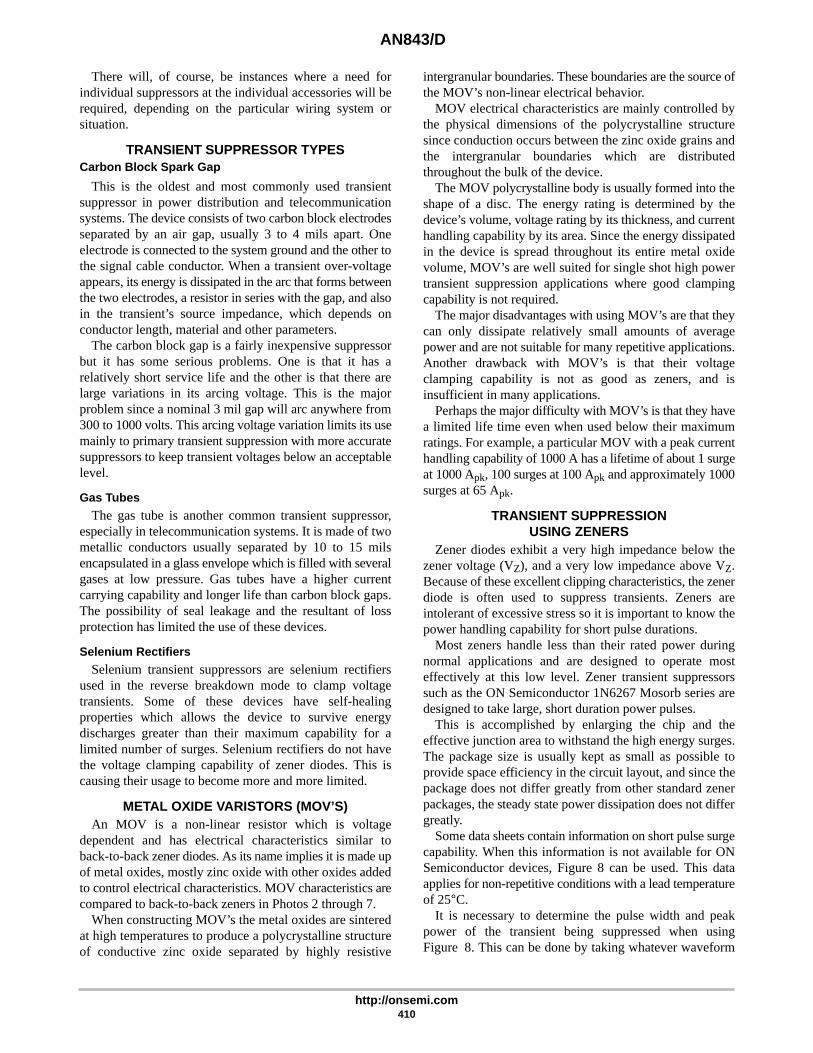
AN843/D
http://onsemi.com410
There will, of course, be instances where a need forindividual suppressors at the individual accessories will berequired, depending on the particular wiring system orsituation.
TRANSIENT SUPPRESSOR TYPESCarbon Block Spark Gap
This is the oldest and most commonly used transientsuppressor in power distribution and telecommunicationsystems. The device consists of two carbon block electrodesseparated by an air gap, usually 3 to 4 mils apart. Oneelectrode is connected to the system ground and the other tothe signal cable conductor. When a transient over-voltageappears, its energy is dissipated in the arc that forms betweenthe two electrodes, a resistor in series with the gap, and alsoin the transient’s source impedance, which depends onconductor length, material and other parameters.
The carbon block gap is a fairly inexpensive suppressorbut it has some serious problems. One is that it has arelatively short service life and the other is that there arelarge variations in its arcing voltage. This is the majorproblem since a nominal 3 mil gap will arc anywhere from300 to 1000 volts. This arcing voltage variation limits its usemainly to primary transient suppression with more accuratesuppressors to keep transient voltages below an acceptablelevel.
Gas Tubes
The gas tube is another common transient suppressor,especially in telecommunication systems. It is made of twometallic conductors usually separated by 10 to 15 milsencapsulated in a glass envelope which is filled with severalgases at low pressure. Gas tubes have a higher currentcarrying capability and longer life than carbon block gaps.The possibility of seal leakage and the resultant of lossprotection has limited the use of these devices.
Selenium Rectifiers
Selenium transient suppressors are selenium rectifiersused in the reverse breakdown mode to clamp voltagetransients. Some of these devices have self-healingproperties which allows the device to survive energydischarges greater than their maximum capability for alimited number of surges. Selenium rectifiers do not havethe voltage clamping capability of zener diodes. This iscausing their usage to become more and more limited.
METAL OXIDE VARISTORS (MOV’S)An MOV is a non-linear resistor which is voltage
dependent and has electrical characteristics similar toback-to-back zener diodes. As its name implies it is made upof metal oxides, mostly zinc oxide with other oxides addedto control electrical characteristics. MOV characteristics arecompared to back-to-back zeners in Photos 2 through 7.
When constructing MOV’s the metal oxides are sinteredat high temperatures to produce a polycrystalline structureof conductive zinc oxide separated by highly resistive
intergranular boundaries. These boundaries are the source ofthe MOV’s non-linear electrical behavior.
MOV electrical characteristics are mainly controlled bythe physical dimensions of the polycrystalline structuresince conduction occurs between the zinc oxide grains andthe intergranular boundaries which are distributedthroughout the bulk of the device.
The MOV polycrystalline body is usually formed into theshape of a disc. The energy rating is determined by thedevice’s volume, voltage rating by its thickness, and currenthandling capability by its area. Since the energy dissipatedin the device is spread throughout its entire metal oxidevolume, MOV’s are well suited for single shot high powertransient suppression applications where good clampingcapability is not required.
The major disadvantages with using MOV’s are that theycan only dissipate relatively small amounts of averagepower and are not suitable for many repetitive applications.Another drawback with MOV’s is that their voltageclamping capability is not as good as zeners, and isinsufficient in many applications.
Perhaps the major difficulty with MOV’s is that they havea limited life time even when used below their maximumratings. For example, a particular MOV with a peak currenthandling capability of 1000 A has a lifetime of about 1 surgeat 1000 Apk, 100 surges at 100 Apk and approximately 1000surges at 65 Apk.
TRANSIENT SUPPRESSIONUSING ZENERS
Zener diodes exhibit a very high impedance below thezener voltage (VZ), and a very low impedance above VZ.Because of these excellent clipping characteristics, the zenerdiode is often used to suppress transients. Zeners areintolerant of excessive stress so it is important to know thepower handling capability for short pulse durations.
Most zeners handle less than their rated power duringnormal applications and are designed to operate mosteffectively at this low level. Zener transient suppressorssuch as the ON Semiconductor 1N6267 Mosorb series aredesigned to take large, short duration power pulses.
This is accomplished by enlarging the chip and theeffective junction area to withstand the high energy surges.The package size is usually kept as small as possible toprovide space efficiency in the circuit layout, and since thepackage does not differ greatly from other standard zenerpackages, the steady state power dissipation does not differgreatly.
Some data sheets contain information on short pulse surgecapability. When this information is not available for ONSemiconductor devices, Figure 8 can be used. This dataapplies for non-repetitive conditions with a lead temperatureof 25°C.
It is necessary to determine the pulse width and peakpower of the transient being suppressed when usingFigure 8. This can be done by taking whatever waveform

AN843/D
http://onsemi.com411
the transient is and approximating it with a rectangular pulsewith the same peak power. For example, an exponentialdischarge with a 1 ms time constant can be approximated bya rectangular pulse 1 ms wide that has the same peak poweras the transient. This would be a better approximation thana rectangular pulse 10 ms wide with a correspondingly loweramplitude. This is because the heating effects of differentpulse width lengths affect the power handling capability, ascan be seen by Figure 8. This also represents a conservativeapproach because the exponential discharge will contain ≈1/2 the energy of a rectangular pulse with the same pulsewidth and amplitude.
Figure 8. Peak Power Ratings of Zener Diodes
1N6267 SERIES
GLASS DO35 & GLASS DO41250 mW TO 1 W TYPES
5 WATT TYPES
PULSE WIDTH (ms)
0.1
100
0.01 0.02
PP
K(N
OM
), N
OM
INA
L P
EA
K P
OW
ER
(kW
)
50
20
10
5
2
1
0.5
0.2
0.1
0.05
0.020.01
0.05 0.2 0.5 1 2 5 10
1 TO 3 W TYPESPLASTIC DO41
When used in repetitive applications, the peak power mustbe reduced as indicated by the curves of Figure 9. Averagepower must be derated as the lead or ambient temperatureexceeds 25°C. The power derating curve normally given ondata sheets can be normalized and used for this purpose.
Figure 9. Typical Derating Factor for Duty Cycle
0.1
1
0.7
0.5
0.3
0.2
0.02
0.1
0.07
0.05
0.03
0.010.2 0.5 1 52 10 20 50
PULSE WIDTH10 ms
1 ms
100 µs
10 µs
D, DUTY CYCLE (%)
DE
RAT
ING
FA
CT
OR
The peak zener voltage during the peak current of thetransient being suppressed can be related to the nominalzener voltage (Eqtn 1) by the clamping factor (FC).
Eqtn 1: VZ(pK) = FC (VZ(nom))
Unless otherwise specified FC is approximately 1.20 forzener diodes when operated at their pulse power limits.
For example, a 5 watt, 20 volt zener can be expected toshow a peak voltage of 24 volts regardless of whether it ishandling 450 watts for 0.1 ms or 50 watts for 10 ms. (SeeFigure 8.)
This occurs because the zener voltage is a function of bothjunction temperature and IR drop. Longer pulse widthscause a greater junction temperature rise than short ones; theincrease in junction temperature slightly increases the zenervoltage. This increase in zener voltage due to heating isroughly offset by the fact that longer pulse widths ofidentical energy content have lower peak currents. Thisresults in a lower IR drop (zener voltage drop) keeping theclamping factor relatively constant with various pulsewidths of identical energy content.
An approximation of zener impedance is also helpful inthe design of transient protection circuits. The value ofRZ(nom) (Eqtn 2) is approximate because both the clampingfactor and the actual resistance is a function of temperature.
Eqtn 2: RZ(nom) =V2
Z(nom) (FC –1)
PpK(nom)
VZ(nom) = Nominal Zener VoltagePpK(nom) = Found from Figure 8 when device type andpulse width are known. For example, from Figure 8 a1N6267 zener suppressor has a PpK(nom) of 1.5 kW at apulse width of 1 ms.As seen from equation 2, zeners with a larger PpK(nom)
capability will have a lower RZ(nom).
ZENER versus MOV TRADEOFFSThe clamping characteristics of Zeners and MOV’s are
best compared by measuring their voltages under transientconditions. Photos 1 through 9 are the result of anexperiment that was done to compare the clampingcharacteristics of a Zener (ON Semiconductor 1N6281,approximately 1.5J capability) with those of an MOV (G.E.V27ZA4, 4J capability); both are 27 V devices.
Photo 1 shows the pulse generator output voltage. Thisgenerator synthesizes a transient pulse that is characteristicof those that may appear in the real world.
Photos 2 and 3 are clamping voltages of the MOV andZener, respectively with a surge source impedance of 500 Ω.
Photos 4 and 5 are the clamping voltages with a surgesource impedance of 50 Ω.
Photos 6 and 7 simulate a condition where the surgesource impedance is 5 Ω.
Photos 8 and 9 show a surge source impedance of 0.55 Ω,which is at the limits of the Zener suppressor’s capability.

AN843/D
http://onsemi.com412
PHOTO 1Open Circuit Transient PulseVert: 20 V/divHoriz: 0.5 ms/divVpeak = 90 V
PHOTO 2MOV (27 V)Vert: 10 V/divHoriz: 0.5 ms/divTransient Source Impedance: 500 ΩVpeak = 39.9 V
0%
10090
10
0%
10090
10

AN843/D
http://onsemi.com413
PHOTO 3Zener (27 V)Vert: 10 V/divHoriz: 0.5 ms/divTransient Source Impedance: 500 ΩVpeak = 27 V
PHOTO 4MOV (27 V)Vert: 10 V/divHoriz: 0.5 ms/divTransient Source Impedance: 50 ΩVpeak = 44.7 V
PHOTO 5Zener (27 V)Vert: 10 V/divHoriz: 0.5 ms/divTransient Source Impedance: 50 ΩVpeak = 27 V
0%
10090
10
0%
10090
10
0%
10090
10
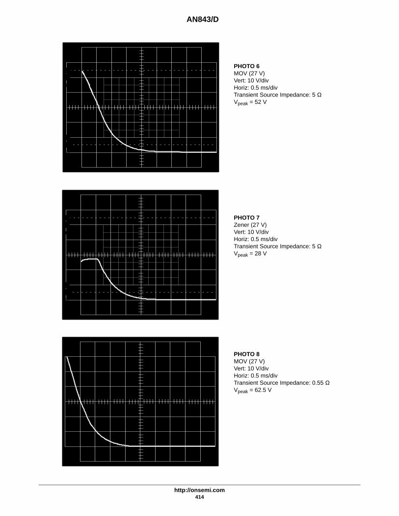
AN843/D
http://onsemi.com414
PHOTO 6MOV (27 V)Vert: 10 V/divHoriz: 0.5 ms/divTransient Source Impedance: 5 ΩVpeak = 52 V
PHOTO 7Zener (27 V)Vert: 10 V/divHoriz: 0.5 ms/divTransient Source Impedance: 5 ΩVpeak = 28 V
PHOTO 8MOV (27 V)Vert: 10 V/divHoriz: 0.5 ms/divTransient Source Impedance: 0.55 ΩVpeak = 62.5 V
0%
10090
10
0%
10090
10

AN843/D
http://onsemi.com415
PHOTO 9Zener (27 V)Vert: 10 V/divHoriz: 0.5 ms/divTransient Source Impedance: 0.55 ΩVpeak: 30.2 VPeak Power: Approx 2000 Wpeak(The limit of this device’s capability)
As can be seen by the photographs, the Zener suppressorhas significantly better voltage clamping characteristicsthan the MOV even though that particular Zener has lessthan one-fourth the energy capability of the MOV it wascompared with. However, the energy rating can bemisleading because it is based on the clamp voltage times thesurge current, and when using an MOV, the high impedanceresults in a fairly high clamp voltage. The major tradeoffwith using a zener type suppressor is its cost versus powerhandling capability, but since it would take an “oversized”MOV to clamp voltages (suppress transients) as well as thezener, the MOV begins to lose its cost advantage.
If a transient should come along that exceeds thecapabilities of the particular Zener, or MOV, suppressor thatwas chosen, the load will still be protected, since they bothfail short.
The theoretical reaction time for Zeners is in thepicosecond range, but this is slowed down somewhat withlead and package inductance. The 1N6267 Mosorb series oftransient suppressors have a typical response time of lessthan one nanosecond. For very fast rising transients it isimportant to minimize external inductances (due to wiring,etc.) which will minimize overshoot.
Connecting Zeners in a back-to-back arrangement willenable bidirectional voltage clamping characteristics. (SeeFigure 10.)
If Zeners A and B are the same voltage, a transient ofeither polarity will be clamped at approximately that voltagesince one Zener will be in reverse bias mode while the otherwill be in the forward bias mode. When clamping lowvoltage it may be necessary to consider the forward drop ofthe forward biased Zener.
The typical protection circuit is shown in Figure 11a. Inalmost every application, the transient suppression device isplaced in parallel with the load, or component to beprotected. Since the main purpose of the circuit is to clampthe voltage appearing across the load, the suppressor should
be placed as close to the load as possible to minimizeovershoot due to wiring (or any inductive) effect. (SeeFigure 11b.)
Figure 10. Zener Arrangement forBidirectional Clamping
Figure 11a. Using Zener to Protect LoadAgainst Transients
ÎÎÎÎÎÎ
OR
B
A
Vin
Zin
B
A
LOAD VL
Figure 11b. Overshoot Due to Inductive Effect
ZENER
VOLTAGE
PEAK VOLTAGE
DUE TO OVERSHOOT
TRANSIENT
INPUT

AN843/D
http://onsemi.com416
Zener capacitance prior to breakdown is quite small (forexample, the 1N6281 27 Volt Mosorb has a typicalcapacitance of 800 pF). Capacitance this small is desirablein the off-state since it will not attenuate wide-band signals.
When the Zener is in the breakdown mode of operation(e.g. when suppressing a transient) its effective capacitanceincreases drastically from what it was in the off-state. Thismakes the Zener ideal for parallel protection schemes since,during transient suppression, its large effective capacitancewill tend to hold the voltage across the protected elementconstant; while in the off-state (normal conditions, notransient present), its low off-state capacitance will notattenuate high frequency signals.
Input impedance (Zin) always exists due to wiring andtransient source impedance, but Zin should be increased asmuch as possible with an external resistor, if circuitconstraints allow. This will minimize Zener stress.
CONCLUSIONThe reliable use of semiconductor devices requires that
the circuit designer consider the possibility of transientovervoltages destroying these transient-sensitivecomponents.
These transients may be generated by normal circuitoperations such as inductive switching circuits, energizingand deenergizing transformer primaries, etc. They do notpresent much of a problem since their energy content,duration and effect may easily be obtained and dealt with.
Random transients found on power lines, or lightningtransients, present a greater threat to electronic componentssince there is no way to be sure when or how severe they willbe. General guidelines were discussed to aid the circuitdesigner in deciding what size (capability and cost)suppressor to choose for a certain level of protection. Therewill always be a tradeoff between suppressor price andprotection obtained.
Several different suppression devices were discussed withemphasis on Zeners and MOV’s, since these are the mostpopular devices to use in most applications.
REFERENCES1. GE Transient Voltage Suppression Manual, 2nd
edition.
2. ON Semiconductor Zener Diode Manual.

http://onsemi.com417
DESIGN CONSIDERATIONS AND PERFORMANCEOF ON SEMICONDUCTOR TEMPERATURE-COMPENSATED
ZENER (REFERENCE) DIODES
Prepared byZener Diode EngineeringandRonald N. RacinoReliability and Quality Assurance
INTRODUCTION
This application note defines ON Semiconductortemperature-compensated zener (reference) diodes,explains the device characteristics, describes electricaltesting, and discusses the advanced concepts of devicereliability and quality assurance. It is a valuable aid to thosewho contemplate designing circuits requiring the use ofthese devices.
Zener diodes fall into three general classifications:Regulator diodes, reference diodes and transient voltagesuppressors. Regulator diodes are normally employed inpower supplies where a nearly constant dc output voltage isrequired despite relatively large changes in input voltage orload resistance. Such devices are available with a wide rangeof voltage and power ratings, making them suitable for awide variety of electronic equipments.
Regulator diodes, however, have one limitation: They aretemperature-sensitive. Therefore, in applications in whichthe output voltage must remain within narrow limits duringinput-voltage, load-current, and temperature changes, atemperature-compensated regulator diode, called areference diode, is required.
The reference diode is made possible by taking advantageof the differing thermal characteristics of forward- andreverse-biased silicon p-n junctions. A forward-biasedjunction has a negative temperature coefficient ofapproximately 2 mV/°C, while reverse-biased junctionshave positive temperature coefficients ranging from about2 mV/°C at 5.5 V to 6 mV/°C at 10 V. Therefore it ispossible, by judicious combination of forward- andreverse-biased junctions, to fabricate a device with a verylow overall temperature coefficient (Figure 1).
The principle of temperature compensation is furtherillustrated in Figure 2, which shows the voltage-currentcharacteristics at two temperature points (25 and 100°C) forboth a forward- and a reverse-biased junction. The diagramshows that, at the specified test current (IZT), the absolutevalue of voltage change (∆V) for the temperature changebetween 25 and 100°C is the same for both junctions.Therefore, the total voltage across the combination of thesetwo junctions is also the same at these temperature points,since one ∆V is negative and the other is positive. However,the rate of voltage change with temperature over the
Figure 1. Temperature Compensationof a 6.2 Volt Reference Diode (1N821 Series)
DIO
DE
VO
LTA
GE
DR
OP
(V
)(R
EF
ER
EN
CE
D T
O I Z
T=
7.5
mA
)
6.4
6.2
6
5.8
5.6
5.4
0.8
0.6
0.4
0.2
0-75 -50 -25 0 +25 +50 +75 +100
TEMPERATURE (°C)
6.2 - VOLT REFERENCE DIODE(COMBINATION OF ZENER
AND FORWARD DICE)
ZENER DIE
FORWARDBIASED COMPENSATING DIE
temperature range defined by these points is not necessarilythe same for both junctions, thus the temperaturecompensation may not be linear over the entire range.
Figure 2 also indicates that the voltage changes of the twojunctions are equal and opposite only at the specified testcurrent. For any other value of current, the temperaturecompensation may not be complete.

http://onsemi.com418
Figure 2. Temperature Compensation ofP-N Junctions
DIRECTION OF CURRENT FLOW
PACKAGE
OUTLINE25°C
100°C
VF
+
I
IZT
-∆V
+∆V
25°CVR I
100°C
IZT-
FORWARDBIASED
PN JUNCTION
REVERSEBIASED
ZENER JUNCTION
IMPORTANT ELECTRICAL CHARACTERISTICSOF REFERENCE DIODES
The three most important characteristics of referencediodes are 1) reference voltage, 2) voltage-temperaturestability, and 3) voltage-time stability.
1. Reference Voltage. This characteristic is defined as thevoltage drop measured across the diode when the specifiedtest current passes through it in the zener direction. It is alsocalled the zener voltage (VZ, Figure 3). On the data sheets,the reference voltage is given as a nominal voltage for eachfamily of reference diodes.
The nominal voltages are normally specified to atolerance of ±5%, but devices with tighter tolerances, suchas ±2% and ±1%, are available on special order.
2. Voltage-Temperature Stability. The temperaturestability of zener voltage is sometimes expressed by meansof the temperature coefficient. This parameter is usuallydefined as the percent voltage change across the device perdegree centigrade. This method of indicating voltagestability accurately reflects the voltage deviation at the testtemperature extremes but not necessarily at other pointswithin the specified temperature range. This fact is due tovariations in the rate of voltage change with temperature forthe forward- and reverse-biased dice of the reference diode.Therefore, the temperature coefficient is given inON Semiconductor data sheets only as a quick reference,for designers who are accustomed to this method ofspecification.
A more meaningful way of defining temperature stabilityis the “box method.” This method, used byON Semiconductor, guarantees that the zener voltage willnot vary by more than a specified amount over a specifiedtemperature range at the indicated test current, as verified bytests at several temperatures within this range.
Some devices are accurately compensated over a widetemperature range (–55°C to 100°C), others over a narrowerrange (0 to 75°C). The wide-range devices are, as a rule,more expensive. Therefore, it would be economicallywasteful for the designer to specify devices with atemperature range much wider than actually required for thespecific device application.
During actual production of reference diodes, it is difficultto predict the compensation accuracy. In the interest ofmaximum economy, it is common practice to test all devicescoming off the production line, and to divide the productionlot into groups, each with a specified maximum ∆VZ. Eachgroup, then, is given a different device type number.
Figure 3. Typical Voltage – Current Characteristic of Reference Diodes
I F(m
A)
0.3
0.2
0.1
-6 -4 -2
-0.1
-0.2
-0.3
2 4 6 8 10 12 14 16
VF (V)
I R(m
A)
VR (V)
IZVZ

http://onsemi.com419
On the data sheet, the voltage-temperature characteristicsof the most widely used device types are illustrated in agraph similar to the one shown in Figure 4. The particularproduction line represented in this figure produces 6.2 voltdevices, but the line yields five different device typenumbers (1N821 through 1N829), each with a differenttemperature coefficient. The 1N829, for example, has amaximum voltage change of less than 5 mV over atemperature range of –55 to +100°C, while the 1N821 mayhave a voltage change of up to 96 mV over the sametemperature range.
Figure 4. Temperature Dependenceof Zener Voltage (1N821 Series)
∆VZ = +31 mV
∆VZ = -31 mV
IZT = 7.5 mA
1N821,A
1N823,A
1N825,A
1N829,A
1N827,A
1N827,A
1N825,A
1N823,A
1N821,A
100
75
50
25
0
-25
-50
-75
-100-55 0 50 100
∆V
Z, M
AX
IMU
M V
OLT
AG
E C
HA
NG
E (
mV
)(R
efer
ence
d to
-55
°C)
In the past, design data and characteristic curves on data sheets forreference diodes have been somewhat limited: The devices havebeen characterized principally at the recommended operating point.ON Semiconductor has introduced a data sheet, providing devicedata previously not available, and showing limit curves that permitworst-case circuit design without the need for associated tests re-quired in conjunction with the conventional data sheets.
Graphs such as these permit the selection of thelowest-cost device that meets a particular requirement. Theyalso permit the designer to determine the maximum voltagechange of a particular reference diode for a relatively smallchange in temperature. This is done by drawing vertical linesfrom the desired temperature points at the abscissa of thegraph to intersect with each the positive- and negative-goingcurves of the particular device of interest. Horizontal linesare then drawn from these intersects to the ordinate of thegraph. The difference between the intersections of thesehorizontal lines with the ordinate yields the maximumvoltage change over the temperature increment. Forexample, for the 1N821, a change in ambient temperaturefrom 0 to 50°C results in a voltage change of no more thanabout ±31 mV.
The reason that the device reference voltage may changein either the negative or positive direction is that afterassembly, some of the devices within a lot may beovercompensated while others may be undercompensated.In any design, the “worst-case” condition must beconsidered. Therefore, in the above example, it can beassumed that the maximum voltage change will not exceed31 mV.
It should be understood, however, that the abovecalculations give the maximum possible voltage change forthe device type, and by no means the actual voltage changefor the individual unit.
3. Voltage-Time Stability. The voltage-time stability ofa reference diode is defined by the voltage change duringoperating time at the standard test current (IZT) and testtemperature (TA). In general, the voltage stability of areference diode is better than 100 ppm per 1000 hours ofoperation.
Figure 5. Current Dependence of Zener Voltageat Various Temperatures
(1N821 Series)
I Z, Z
EN
ER
CU
RR
EN
T (m
A)
10
9
8
7.5
7
6
5
4-75 -50 -25 0 25 50
+100°C
IZT
+25°C
-55°C
+25°C
+100°C-55°C
∆VZ, MAXIMUM VOLTAGE CHANGE (mV)
(Referenced to IZT = 7.5 mA)
THE EFFECT OF CURRENT VARIATION ONZENER VOLTAGE
The nominal zener voltage of a reference diode isspecified at a particular value of current, called the zener testcurrent (IZT). All measurements of voltage change withtemperature are referenced to this test current. If theoperating current is varied, all these specifications willchange.
The effect of current variation on zener voltage, at varioustemperatures, is graphically illustrated on the 1N821 datasheet as “Zener Current versus Maximum Voltage Change.”A typical example of such a graph is shown for the 1N821series in Figure 5. The voltage change shown is due entirelyto the impedance of the device at the fixed temperature. Itdoes not reflect the change in reference voltage due to thechange in temperature since each curve is referenced to IZT= 7.5 mA at the indicated temperature. As shown, the

http://onsemi.com420
greatest voltage change occurs at the highest temperaturerepresented in the diagram. (See “Dynamic Impedance”under the next section).
Figure 5 shows that, at 25°C, a change in zener currentfrom 4 to 10 mA causes a voltage shift of about 90 mV.Comparing this value with the voltage-change example inFigure 4 (31 mV), it is apparent that, in general, a greatervoltage variation may be due to current fluctuations than totemperature change. Therefore, good current regulation ofthe source should be a major consideration when usingreference diodes in critical applications.
It is not essential, however, that a reference diode beoperated at the specified test current. The newvoltage-temperature characteristics for a change in currentcan be obtained by superimposing the data of Figure 5 onthat of Figure 4. A new set of characteristics, at a test currentof 4 mA, is shown for the 1N823 in Figure 6, together withthe original characteristics at 7.5 mA.
Figure 6. Voltage Change with Temperaturefor 1N823 at Two Different Current Levels
+100
+50
0
-50
-100
-150
-200-50 0 50 100
7.5 mA
4 mA
TEMPERATURE (°C)
V Z(m
V)
(RE
FE
RE
NC
ED
TO
-55
C)
°∆
From these characteristics, it is evident that the voltagechange with temperature for the new curves is different fromthat for the original ones. It is also apparent that if the testcurrent varies between 7.5 and 4 mA, the voltage changeswould lie along the dashed lines belonging to the giventemperature points. This clearly shows the need for awell-regulated current source.
It should be noted, however, that even when awell-regulated current supply is available, other factorsmight influence the current flowing through a referencediode. For example, to minimize the effects oftemperature-sensitive passive elements in the load circuit oncurrent regulation, it is desirable that the load in parallel withthe reference diode have an impedance much higher than thedynamic impedance of the reference diode.
OTHER CHARACTERISTICS
In addition to the three major characteristics discussedearlier, the following parameters and ratings of referencediodes may be considered in some applications.
Power Dissipation
The maximum dc power dissipation indicates the powerlevel which, if exceeded, may result in the destruction of thedevice. Normally a device will be operated near thespecified test current for which the data-sheet specificationsare applicable. This test current is usually much below thecurrent level associated with the maximum powerdissipation.
Dynamic Impedance
Zener impedance may be construed as composed of acurrent-dependent resistance shunted by avoltage-dependent capacitance. Figure 7 indicates thetypical variations of dynamic zener impedance (ZZ) withcurrent and temperature for the 1N821 reference diodeseries. These diagrams are given in the 1N821 data sheet. Asshown, the zener impedance decreases with current butincreases with ambient temperature.
Figure 7. Variation of Zener ImpedanceWith Current and Temperature (1N821 Series)
1000800600400
200
100806040
20
10864
2
11 2 4 6 8 10 20 40 60 80 100
IZ, ZENER CURRENT (mA)
ZZ
, MA
XIM
UM
ZE
NE
R IM
PE
DA
NC
E (
OH
MS
)
-55°C
25°C
100°C
The impedance of a reference diode is normally specifiedat the test current (IZT). It is determined by measuring the acvoltage drop across the device when a 60 Hz ac current withan rms value equal to 10% of the dc zener current issuperimposed on the zener current (IZT). Figure 8 shows theblock diagram of a circuit used for testing zener impedance.
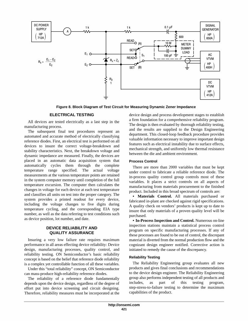
http://onsemi.com421
Figure 8. Block Diagram of Test Circuit for Measuring Dynamic Zener Impedance
DC POWER
SUPPLY
88i8.88888
HP712A
A
88i8.88888
HP650A
SIGNAL
GENERATOR
88i8.88888
HP400H
AC
VTVM
88i8.88888
HP412A
DC
VTVM
METER
DUMMY
LOAD
600
0.1µF1k1k
E1
E2
Rx=Zz
READ
SET
READ
SET (B)
S1
(A) 10M
100pF
R2
1
Rx=E1-E2
E2
ELECTRICAL TESTING
All devices are tested electrically as a last step in themanufacturing process.
The subsequent final test procedures represent anautomated and accurate method of electrically classifyingreference diodes. First, an electrical test is performed on alldevices to insure the correct voltage-breakdown andstability characteristics. Next, the breakdown voltage anddynamic impedance are measured. Finally, the devices areplaced in an automatic data acquisition system thatautomatically cycles them through the completetemperature range specified. The actual voltagemeasurements at the various temperature points are retainedin the system computer memory until completion of the fulltemperature excursion. The computer then calculates thechanges in voltage for each device at each test temperatureand classifies all units on test into the proper category. Thesystem provides a printed readout for every device,including the voltage changes to five digits duringtemperature cycling, and the corresponding EIA typenumber, as well as the data referring to test conditions suchas device position, lot number, and date.
DEVICE RELIABILITY ANDQUALITY ASSURANCE
Insuring a very low failure rate requires maximumperformance in all areas effecting device reliability: Devicedesign, manufacturing processes, quality control, andreliability testing. ON Semiconductor’s basic reliabilityconcept is based on the belief that reference diode reliabilityis a complex yet controllable function of all these variables.
Under this “total reliability” concept, ON Semiconductorcan mass-produce high-reliability reference diodes.
The reliability of a reference diode fundamentallydepends upon the device design, regardless of the degree ofeffort put into device screening and circuit designing.Therefore, reliability measures must be incorporated at the
device design and process development stages to establisha firm foundation for a comprehensive reliability program.The design is then evaluated by thorough reliability testing,and the results are supplied to the Design Engineeringdepartment. This closed-loop feedback procedure providesvaluable information necessary to improve important designfeatures such as electrical instability due to surface effects,mechanical strength, and uniformly low thermal resistancebetween the die and ambient environment.
Process Control
There are more than 2000 variables that must be keptunder control to fabricate a reliable reference diode. Thein-process quality control group controls most of thesevariables. It places a strict controls on all aspects ofmanufacturing from materials procurement to the finishedproduct. Included in this broad spectrum of controls are:
• Materials Control. All materials purchased orfabricated in-plant are checked against rigid specifications.A quality check on vendors’ products is kept up to date toinsure that only materials of a proven quality level will bepurchased.
• In-Process Inspection and Control. Numerous on-lineinspection stations maintain a statistical process controlprogram on specific manufacturing processes. If any ofthese processes are found to be out of control, the discrepantmaterial is diverted from the normal production flow and thecognizant design engineer notified. Corrective action isinitiated to remedy the cause of the discrepancy.
Reliability Testing
The Reliability Engineering group evaluates all newproducts and gives final conclusions and recommendationsto the device design engineer. The Reliability Engineeringgroup also performs independent testing of all products andincludes, as part of this testing program,step-stress-to-failure testing to determine the maximumcapabilities of the product.

http://onsemi.com422
SOME STRAIGHT TALK ABOUT MOSORBSTRANSIENT VOLTAGE SUPPRESSORS
INTRODUCTION
Distinction is sometimes made between devicestrademarked Mosorb (by ON Semiconductor Inc.), andstandard zener/avalanche diodes used for reference,low-level regulation and low-level protection purposes. Itmust be emphasized from the beginning that Mosorbdevices are, in fact, zener diodes. The basic semiconductortechnology and processing are identical. The primarydifference is in the applications for which they are designed.Mosorb devices are intended specifically for transientprotection purposes and are designed, therefore, with a largeeffective junction area that provides high pulse powercapability while minimizing the total silicon use. Thus,Mosorb pulse power ratings begin at 500 watts – well inexcess of low power conventional zener diodes which inmany cases do not even include pulse power ratings amongtheir specifications.
MOVs, like Mosorbs, do have the pulse powercapabilities for transient suppression. They are metal oxidevaristors (not semiconductors) that exhibit bidirectionalavalanche characteristics, similar to those of back-to-backconnected zeners. The main attributes of such devices arelow manufacturing cost, the ability to absorb high energysurges (up to 600 joules) and symmetrical bidirectional“breakdown” characteristics. Major disadvantages are: highclamping factor, an internal wear-out mechanism and anabsence of low-end voltage capability. These limitationsrestrict the use of MOVs primarily to the protection ofinsensitive electronic components against high energytransients in application above 20 volts, whereas, Mosorbsare best suited for precise protection of sensitive equipmenteven in the low voltage range – the same range covered byconventional zener diodes. The relative features of the twodevice types are covered in Table 1.
IMPORTANT SPECIFICATIONS FORMOSORB PROTECTIVE DEVICES
Typically, a Mosorb suppressor is used in parallel with thecomponents or circuits being protected (Figure 1), in orderto shunt the destructive energy spike, or surge, around themore sensitive components. It does this by avalanching at its“breakdown” level, ideally representing an infiniteimpedance at voltages below its rated breakdown voltage,and essentially zero impedance at voltages above this level.
In the more practical case, there are three voltagespecifications of significance, as shown in Figure 1a.
a) VRWM is the maximum reverse stand-off voltage atwhich the Mosorb is cut off and its impedance is at itshighest value – that is, the current through the device isessentially the leakage current of a back-biased diode.
b) V(BR) is the breakdown voltage – a voltage at which thedevice is entering the avalanche region, as indicated bya slight (specified) rise in current beyond the leakagecurrent.
c) VRSM is the maximum reverse voltage (clampingvoltage) which is defined and specified in conjunctionwith the maximum reverse surge current so as not toexceed the maximum peak power rating at a pulsewidth (tp) of 1 ms (industry std time for measuringsurge capability).
RELATIVE FEATURES OF MOVs and MOSORBS
Table 1.
MOV Mosorb/Zener Transient Suppressor
• High clamping factor.• Symmetrically bidirectional.
• Energy capability per dollar usually higher than a silicon device.However, if good clamping is required the energy capability wouldhave to be grossly overspecified resulting in higher cost.
• Inherent wear out mechanism clamp voltage degrades after everypulse, even when pulsed below rated value.
• Ideally suited for crude ac line protection.• High single-pulse current capability.• Degrades with overstress.• Good high voltage capability.• Limited low voltage capability.
• Very good clamping close to the operating voltage.• Standard parts perform like standard zeners. Symmetrical bidirec-
tional devices available for many voltages.• Good clamping characteristic could reduce overall system cost.
• No inherent wear out mechanism.
• Ideally suited for precise DC protection.• Medium multiple-pulse current capability.• Fails short with overstress.• Limited high voltage capability unless series devices are used.• Good low voltage capability.

http://onsemi.com423
In practice, the Mosorb is selected so that its VRWM isequal to or somewhat higher than the highest operatingvoltage required by the load (the circuits or components tobe protected). Under normal conditions, the Mosorb isinoperative and dissipates very little power. When atransient occurs, the Mosorb converts to a very low dynamicimpedance and the voltage across the Mosorb becomes theclamping voltage at some level above V(BR). The actualclamping level will depend on the surge current through theMosorb. The maximum reverse surge current (IRSM) isspecified on the Mosorb data sheets at 1 ms and for alogrithmically decaying pulse waveform. The data sheetalso contains curves to determine the maximum surgecurrent rating at other time intervals.
Typically, Mosorb devices have a built-in safety margin atthe maximum rated surge current because the clamp voltage,VRSM, is itself, guardbanded. Thus, the parts will beoperating below their maximum pulse-power (Ppk) ratingeven when operated at maximum reverse surge current).
If the transients are random in nature (and in many casesthey are), determining the surge-current level can be aproblem. The circuit designer must make a reasonableestimate of the proper device to be used, based on hisknowledge of the system and the possible transients to beencountered. (e.g., transient voltage, source impedance andtime, or transient energy and time are some characteristicsthat must be estimated). Because of the very low dynamicimpedance of Mosorb devices in the region between V(BR)and VRSM, the maximum surge current is dependent on, andlimited by the external circuitry.
In cases where this surge current is relatively low, aconventional zener diode could be used in place of a Mosorbor other dedicated protective device with some possiblesavings in cost. The surge capabilities most ofON Semiconductor’s zener diode lines are discussed inON Semiconductor’s Application Note AN784.
In the data sheets of some protective devices, theparameter for response time is emphasized. Response timeon these data sheets is defined as the time required for thevoltage across the protective device to rise from 0 to V(BR),and relates primarily to the effective series impedanceassociated with the device. This effective impedance issomewhat complex and changes drastically from theblocking mode to the avalanche mode. In most applications(where the protective device shunts the load) this responsetime parameter becomes virtually meaningless as indicatedby the waveforms in Figures 1b and 1c. If the response timeas defined is very long, it still would not affect theperformance of the surge suppressor.
However, if the series inductance becomes appreciable, itcould result in “overshoot” as shown in Figure 1d that wouldbe detrimental to circuit protection. In Mosorb devices,series inductance is negligible compared to the inductiveeffects of the external circuitry (primarily lead lengths).Hence, Mosorbs contribute little or nothing to overshootand, in essence, the parameter of response time has very littlesignificance. However, care must be exercised in the designof the external circuitry to minimize overshoot.
SUMMARY
In selecting a protective device, it is important to know asmuch as possible about the transient conditions to beencountered. The most important device parameters arereverse working voltage (VRWM), surge current (IRSM), andclamp voltage (VRSM). the product of VRSM and IRSM yieldsthe peak power dissipation, which is one of the primecategories for device selection.
The selector guide, in this book, gives a broad overviewof the Mosorb transient suppressors now available from ONSemiconductor. For more detailed information, pleasecontact your ON Semiconductor sales representative ordistributor.

http://onsemi.com424
Figure 1a. Figure 1b.
Figure 1.
Figure 1c. Figure 1d.
MOSORB
PROTECTED
LOAD
Z
OVERSHOOT
VOLTAGE
VRSM
TIME
V(BR)VRWM
tp
Vin
Vout
tclamping, VERY SHORT
VOLTAGE
TIME
VRSM
V(BR)VRWM
Vout
Vin
VOLTAGE
TIME
VOLTAGE
TIME
VRSM
V(BR)VRWM
VRSM
V(BR)VRWM
Vout
Vin
tclamping, VERY LONG tclamping, WITH OVERSHOOT
Vout
Vin
tp = PULSE WIDTH OF INCOMING TRANSIENT
Vin Vout

http://onsemi.com425
TYPICAL MOSORB APPLICATIONS
+
-
+
-
+
-
MOSORBMOSORBS
AC
INPUT
DC
POWER
SUPPLY
DC Power Supplies Input/Output Regulator Protection
MOSORB MOSORB
IC
VOLTAGE
REGULATOR
MOSORB
MOSORB
MOSORB
MOSORB
IC
OP AMP
+B
-B
Op Amp Protection
+
-
MOSORB
Inductive Switching Transistor Protection
DC
MOTOR
DC Motors – Reduces EMI Memory Protection
Microprocessor Protection
Computer Interface Protection
MOS
MEMORY
+5 V
MOSORBS
I/O
ADDRESS BUS
RAM ROM
DATA BUS
CONTROL BUS
MOSORB MOSORB
VDD
VGG
Gnd
CPU
CLOCK
I/O
KEYBOARD
TERMINAL
PRINTER
ETC.
Gnd
FUNCTIONAL
DECODER
A
B
C
D
MOSORB
-8 V
MOSORB
-10 V
MOSORBS
Vout

http://onsemi.com426
AR450 – CHARACTERIZING OVERVOLTAGE TRANSIENT SUPPRESSORS
Prepared byAl PshaenichON Semiconductor Power Products Division
The use of overvoltage transient suppressors forprotecting electronic equipment is prudent andeconomically justified. For relatively low cost, expensivecircuits can be safely protected by one or even several of thetransient suppressors on the market today. Dictated by thetype and energy of the transient, these suppressors can takeon several forms.
For example, in the telecommunication field, wherelightning induced transients are a problem, such primarysuppressors as gas tubes are often used followed bysecondary, lower energy suppressors. In an industrial orautomotive environment, where transients aresystematically generated by inductive switching, thetransient energy is more well-defined and thus adequatelysuppressed by relatively low energy suppressors. Theselower energy suppressors can be zener diodes, rectifiers withdefined reverse voltage ratings, metal oxide varistors(MOVs), thyristors, and trigger devices, among others. Eachdevice has its own niche: some offer better clamping factorsthan others, some have tighter voltage tolerances, some arehigher voltage devices, others can sustain more energy andstill others, like the thyristor family, have low on-voltages.The designer’s problem is selecting the best device for theapplication.
Thus, the intent of this article is twofold:
1. To describe the operation of the surge current testcircuits used in characterizing lower energy transientsuppressors.
2. To define the attributes of the various suppressors,allowing the circuit designer to make thecost/performance tradeoffs.
Surge suppressors are generally specified withexponentially decaying and/or rectangular current pulses.The exponential surge more nearly simulates actual surgecurrent conditions – capacitor discharges, line and switchingtransients, lightning induced transients, etc., whereasrectangular surge currents are usually easier to implementand control.
To generate an exponential rating, a charged capacitor issimply dumped into the device under test (DUT) and theenergy of each successive pulse increased until the deviceultimately fails. The simplified circuit of Figure 1a describesthe circuit. By varying the size of the capacitor C, thelimiting resistor R2, and the voltage to which C is chargedto, various peak currents and pulse widths (defined to the10% discharge point in this paper) can be obtained. To
Figure 1a. Simplified Exponential Tester
Figure 1b. Simplified Rectangular TesterUsing PNP Switch
Figure 1. Basic Surge Current Testers
C
S1
VIN
R1 R2
S2
IZ
DUT10%
tW
IZ
IZ
DUTIZ
tWRL
VEE
VZ
automate this circuit, the series switches S1 and S2 can bereplaced with appropriately controlled transistors or SCRs.
One method of easily implementing a rectangular surgecurrent pulse is shown in the simplified schematic ofFigure 1b. A PNP transistor switch connected to thepositive supply VEE applies power to the DUT. The currentis obviously set by varying either VEE and/or RL. If however,the transistor switch were replaced with a variable, constantcurrent source, measurement procedures are simplified ashow the limiting resistor need not be selected for variouscurrent conditions.
As in most surge current evaluations, the DUT isultimately subjected to destructive energy (current, voltage,pulse width), the failure points noted, and the derated pointsplotted to produce the energy limitation curve. Of particularinterest is the junction temperature at which the DUTs areoperated, be it near failure or at the specified derated point.This measurement relates to the overall reliability of thesuppressor, i.e., can the suppressor sustain one surge currentpulse or a thousand, and will it be degraded when operatedabove the specified maximum operating temperature?
The Rectangular Current Surge Suppressor Test Circuit tobe described addresses these questions by implementing andmeasuring the rectangular current capability of the

http://onsemi.com427
suppressor and determining the device junction temperatureTJ shortly after the end of the surge current pulse. KnowingTJ, the energy to the DUT can be limited just short of failureand thus a complete surge curve generated with only one, ora few DUTs (Figure 6). Second, with the junctiontemperature known, a reliability factor can be determinedfor a practical application.
CIRCUIT OPERATION FOR THERECTANGULAR CURRENT TESTER
The Surge Suppressor Test Circuit block diagram isshown in Figure 2 with the main blocks being the ConstantCurrent Amplifier supplying IZ to the DUT (a zener diodein this instance) during the power pulse and the DiodeForward Current Switch supplying IF during thetemperature sensing time. These two pulses are appliedsequentially, first the much larger IZ, and then the very smallsense current IF. During the IF time, the forward voltage VFof the diode is measured from which the junctiontemperature of the zener diode can be determined. This issimply done by calibrating the forward biased DUT with aspecified low value of IF in a temperature chamber, one pointat 25°C and a second point at some elevated temperature.The result is the familiar diode forward voltage versustemperature linear plot with a slope of about –2 mV/°C fortypical diodes (Figure 7a). Comparing the plot with the testcircuit measured VF yields the DUT junction temperaturefor that particular pulse width and IZ (Figure 7b).
Figure 2. Surge Suppressor TestCircuit Block Diagram
25 µS
BLANKING
MVGATE
SAMPLE
PULSE
300 µS
SENSE
MV
SHORT
DETECTOR
OPEN
DETECTOR
VFS/H
IZDUT
IF
PULSE
GEN
CLOCK
IZ
IF
The System Clock, Pulse Generator, the severalmonostable multivibrators (25 µs Blanking, Sample Pulseand 300 µs Sense MVs) and Gate are fashioned from three
CMOS gate ICs. The remaining blocks are the Sample andHold (S/H) circuit and two detectors for determining thestatus of failed DUTs, either shorted devices or open.
Shown in Figures 3 and 4 respectively, are the completecircuit and significant waveforms. Clocking for the systemis derived from a CMOS, two inverters, astable MV (gates1A and 1B) whose output triggers the two input NOR gateconfigured monostable MV (gates 1C and 1D) to producethe Pulse Generator output pulse (Figure 4b). Alternatively,a single pulse can be obtained by setting switch S2 to the OneShot position and depressing the pushbutton Start switch S1.Contact bounce is suppressed by the 100 ms MV (gates 4Cand D). Frequency of the astable MV, set by potentiometerR1, can vary from about 200 Hz to 0.9 Hz and the pulsewidth, controlled by R2 and the capacitor timing selectorswitch S3, from about 300 µs to 1.3 s.
The positive going Pulse Generator output feeds theConstant Current Amplifier IZ and turns on, in order, NPNtransistor Q1, PNP transistor Q3, NPN Darlington Q4, PNPPower Darlington Q6 and parallel connected PNP PowerTransistors Q8 and Q9. Transistor Q4 is configured as aconstant current source whose current is set by the variablebase voltage potentiometer R3. Thus, the voltage to thebases of Q6, Q8 and Q9 are also accordingly varied.Transistors Q8 and Q9 (MJ14003, IC continuous of 60 A),also connected as constant current sources with their 0.1 Ωemitter ballasting resistors, consequently can produce arectangular current pulse from a minimum of about 0.5 Aand still have adequate gain for 1 ms pulses of 150A peak.Due to propagation delays of this amplifier, the IZ currentwaveform is as shown in Figure 4f. Since Q8 and Q9 mustbe in the linear region for constant current operation, thesetransistors are power dissipation limited at high currents tothe externally connected power supply V+ of 60 V. Thus themaximum DUT voltage, taking into account the clampingfactor of the device, should be limited to about 50 V. Atwider pulse widths and consequently lower currents beforethe DUT fails, the V+ supply should be proportionallyreduced to minimize Q8, Q9 dissipation. As an example, a28 V surge suppressor operating at 100 ms pulse widths canbe tested to destructive limits with V+ of about 40 V.Although a zener diode is shown as the DUT in theschematic, the test devices can be any rectifier with definedreverse voltage, e.g., surge suppressors.
Immediately after the power pulse is applied to the DUT,the negative going sense pulse from the 300 µs MV (Gate2A, Figure 4e) turns on series connected PNP transistor Q10and NPN transistor Q11 of the Diode Forward CurrentSwitch IF. Sense current, set by current limiting resistorselector switch S4, thus flows up from ground through theforward biased DUT, the limiting resistor, and Q11 to the–15 V supply. The result, by monitoring the cathode of theDUT, is a 300 µs wide, approximately –0.6 V pulse.

http://onsemi.com428
P.W
. M.V
.
SW
S4
5 m
A
RE
D
4D12 13
114C
S1
STA
RT
SW
+15
V0.
001
µF0.
1 µF
47 k
100
k
8 9
100
mS
MV
CO
NTA
CT
BO
UN
CE
1.8M
+15
V
10
2
1A1
1M
U4C
,D(1
/2)
MC
1400
1
47 k
100
k
1 S
HO
TS
WS
24
22 k
1B3
SW S6
270
pF
FR
EE
RU
N
1C6 7
5
FR
EQ
CO
NTR
1
5M
0.01
µF
3D12 13
0.1
CLO
CK
U1
MC
1457
2
5 m
s <
T1
< 1.
2S
47 k
1 k
W
SY
NC
R2
SW S3
0.00
33 µ
F
N
0.4
µF
39 k
5M PW
CO
NT
+15
V
I 2 S
WIT
CH
3.9
k
5.6
k
22 k
10 k
47 k
270
pF
100
k
8 µs
SA
MP
LEP
ULS
E
270
pF
1.2M
390
pF
TR
IAD
F90
X
1D9
1F11
2A1 2
3
2C8 9
10
2D12 13
14
3B5 6
4
3C8 9
103A
1 23
4B6 5
4
4A2 1
3
- +
2 3
+15
V
+15
V
60 µ
s <
T2N
< 8
.5 m
S
14 151E
+15
V47
k
1316
8
330
pF
100
k
2B5 6
4
12
U2
MC
1400
1
25 µ
s M
.V.
300
µsS
EN
SE
M.V
.20
0 µF
25 V
+-
120
V
7 m
s <
T2W
< 1
.1 S
MD
A10
1A
0.1
µF
PW
R O
NLE
D 2
MC
7815
100
k10
k
Q18
2N39
04
390
k
100
k
270
pF
U3
MC
1400
1
µC 79152
RE
D
1.2
k1/
2 W
+
200
µF25
V(2
) 1
10 k
2 W
0.1
Ω25
W
(2)
+15
V
1N91
4
220
pF
+15
V
390
pF
200
µF25
V
DU
T
1N91
4
+15
V
-15
V
0.1
µF +15
V+1
5 V 7
100
µS S
AM
PLE
DE
LAY
M.V
.
P.W
.
4,7
k1
W
25 µ
s
+15
V
Q14
MP
S80
99
2N39
06Q
15
10 k
1 k
SH
OR
T L
ED
#1
RE
D
RE
D
OP
EN
LE
D
100
k
470
1 W
470
1 W
SH
OR
TD
ET
EC
TO
R #
1Q
162N
5060
0.1
µF
0.1
µF43
k
10 k
4.7
k
-15
V
+15
V
0.1
µF
4.7
k
-15
V1
k
0.1
µF1
k0.
1 µF
4.7
k
10 k
0.1
µF
-15
V
Q13
2N48
58
25 k
100
k
(1/2
) M
C14
001
U4A
,B
10 k
100
k
150
k
+15
V
47 k
1 k
5 pF
+15
V
0.1
µF
1N91
4(2
)
MR
821
1.3
k
4.7
k
-15
V
I F S
WIT
CH
0.1
µF
10 k18
030
0
1/2
W82
01.
2 k
10 k
390 22
1/2
W
1 k
3.3
k
12 k
10 m
Ω
100
k
47 k
1 k
1N91
4
10 k
1 k
1/2
W
10 k
1N91
4
0.1
µF
0.1
µF
U8
GA
TE
300
µS
100
µS
8 µS
SE
NS
E
DE
LAY
SA
MP
LE
I 2 V2
DU
T -0.7
+3 V
+15
V
2N50
60Q
17
OP
EN
DE
TE
CT
OR
RE
SE
T S
W S
5
0.1
µF
0.00
1 µF
1
U5A
(1/2
) M
C14
58
0.1
µF
VF
+15
V+ -
5 67
+ -
3 26
8
4
15
7
4
S/H U
7 LF
355
SD
-15
V
+ -
3 26
7
4
U6
LF35
5
CI R
4
+15
V
1 k
0.1
µF
0.00
1 µF
0.00
1Q
122N
3906
SH
OR
TLE
D #
2
47 k
22 k
10 k
Q8
Q9
Q7
2N66
68
V +
≤ 60
V10
.000
µF
75 V
Q5
8599
MP
S
15 k
1/2
W+1
5 V 0.
1 µF
680
1/2
W R3
1 k
2.7
k
10 m
A
560
25 m
A
V2
10
2N62
87
Q6
MP
SA
29Q
4
2N39
06Q
3Q
12N
3904
Q2
2N39
06
+15
V
Q10
2N39
06
Q11
MP
S80
99
U9
SH
OR
TD
ET
#2
+15
V
233
U5B
(1/2
) M
C14
58
I 2
Figure 3. Sur ge Suppressors Sur ge Current Fixture

http://onsemi.com429
For accurate measurements of this pulse amplitude,sample and hold circuitry is employed. This consists of unitygain buffer amp U6, series FET switch Q13 and capacitorhold buffer amp U7. The sample pulse (Figure 4H) to thegate of the FET is delayed about 100 µs (by monostable MVG-2C and G-2D) to allow for switching and thermaltransients to settle down. This pulse is derived from thenegative going, trailing edge output pulse of Gate 2D cuttingoff transistor Q18 for the RC time constant in its base circuit.The result is an approximate 8 µs wide sample pulse.Consequently, the DC output voltage from hold amplifierU7 is a measure of the DUT junction temperature.
Invariably, most DUTs will fail short. When the surgesuppressor tester is in the Free-run Mode, the power pulsesubsequent to the DUT shorting could excessively stress theconstant current drivers Q8 and Q9. To prevent thisoccurrence, the Short Detector circuit was implemented.This circuit consists of comparator U5A, 2 input NOR gateconfigured 25 µs monostable MV (G1E and G1F), GateCircuit G3A, 3B and 3C, and SCR Q16. The 25 µs MV
(Figure 4D) is required to blank out turn-on switchingtransients to produce the waveform shown in Figure 4I.During the power pulse, U5A is normally high for a goodDUT (Figure 4J). This waveform is NOR’d with gate 3B(inverted waveform of Figure 4I) to produce a low level(0 V) gate 3C output (Figure 4K).
If, however, the DUT is shorted, U5A output switches lowresulting in a positive pulse output from G3C. This pulsetriggers the SCR on, lighting the LED in its anode circuit andturning on the PNP transistor Q2 across the emitter-base ofQ3, thus clamping off the IZ power pulse. The circuit (Q16)can be reset by opening switch S5.
By and large, this Short Detector circuit was foundadequate to protect transistors Q8 and Q9. However, forsome wide pulse widths, relatively high current conditions,the propagation delay through the Short Detector was toogreat, resulting in excessive FBSOA (Forward Bias SafeOperating Area) stress on Q8 and Q9. Consequently, a fasterShort Detector #2 was implemented.
Figure 4. Surge Suppressor Test Circuit Waveforms
+15 V-14 V
CLOCK
G1B
PULSE GEN
G1D
PULSE GEN
G1C
25 µS MV
G1E
300 µS
SENSE MV
G2A
IZ
100 µS SAMPLE
DELAY MV G2D
8 µS
SAMPLE PULSE Q8
GATE
G3C
SHORT
COMPARATOR U6A
OPEN SCR
TRIGGER U5B
SHORT SCR
TRIGGER G3C
VF
U6-0.6 V
-14 V
GOOD
SHORT
GOOD
SHORT
GOOD
GOOD
OPEN
OPEN
(4A)
(4B)
(4C)
(4D)
(4E)
(4F)
(4G)
(4H)
(4I)
(4J)
(4K)
(4L)
(4M)

http://onsemi.com430
This circuit, connected to the collectors of Q8 and Q9, usesa differentiating network (R4, C1) to discriminate betweenthe normally relatively slow fall time of the voltage pulse onthe DUT, and the exceedingly fast fall time when the devicefails. Thus, the R4-C1 time constant (5 ns) will only generatea negative going trigger to PNP transistor Q12 when the DUTvoltage collapses during device failure. The positive goingoutput from Q12 resets the flip-flop (gates 4A and 4B), whichturns on the NPN transistor Q14. This transistor suppliesdrive to the two PNP clamp transistors (Q5 and Q7) placedrespectively across the emitter-bases of the high, constantcurrent stages Q6 and Q8 and Q9. Propagation delay is thusminimized, providing greater protection to the power stagesof the tester. As an added safety feature, the positive goingoutput from Gate 3C when Short Detector #1 is activated isalso used to trigger the flip-flop.
On the few occasions when the DUT fails open, then theOpen Detector consisting of comparator U5B and SCR Q17comes into play. This circuit measures the DUT integrityduring the sense time. For a good DUT (VF < –1 V), U5Boutput remains low (see Figures 4L and 4M). However foran open DUT, VF switches to the negative rail and U5B goeshigh, turning on Q17. As in the Short Detector, Q2 clampsoff the IZ power amplifier.
All of the circuitry including the +15 V and –15 Vregulated power supplies are self-contained, with theexception of the V+ supply. For high current, narrow pulsewidth testing, this external supply should have 10 to 15 Acapability. If not, additional energy storing capacitors acrossthe supply output may be required.
CIRCUIT OPERATION FOR THEEXPONENTIAL SURGE CURRENT TESTER
To generate the surge current curve of peak current versusexponential discharge pulse width, the test circuit ofFigure 5 was designed. This tester is an implementation ofthe simplified capacitor discharge circuit shown inFigure 1A, with the PNP high voltage transistor Q2allowing the capacitor C to charge through limiting resistorR1 and a triggered SCR discharging the capacitor. As shownin Figure 5, the DUTs can be of any technology, although thedevice connected to the capacitor and discharge limitingresistor RS is shown as an MOS SCR. It could just as wellhave been an SCR as the DUT or as the switch for the zenerdiode, rectifier, SIDAC, etc., DUTs.
System timing for this Exponential Surge Current Testeris derived from a CMOS quad 2 input NOR gate with gates1A and 1B comprising a non-symmetrical astable MV ofabout 13 seconds on and about one second off (switch S3open). The positive On pulse from gate 1B turns on the 500V power MOSFET Q1 and the following PNP transistor Q2.The extremely high current gain FET allows for the largebase current variation of Q2 with varying supply voltage(V+). This capacitor charging circuit has a 400 V blockingcapability (limited by the VCEO of Q2) and thus the capacitorC1 used should be comparably rated. When operating with
high voltage (V+ = 200 to 350 V) and large capacitors(>3000 µF), the power dissipated in the current limitingresistor R1 can be substantial, thus necessitating theillustrated 20 W rating. For longer charging times, switch S3is closed, doubling the timing capacitor and the astable MVon time.
To discharge capacitor C1 and thereby generate theexponential surge current, the SCR must be fired. Thistrigger is generated by the positive going one second pulsefrom gate 1A being integrated by the R2C2 network, andthen shaped by gates 1C and 1D. The net result of about 100µs time delay from gate 1D ensures noncoincident timingconditions. This pulse output is then differentiated by C3-R3with the positive going leading edge turning on Q3, Q4 andfinally the SCR with about a 4 ms wide, 15 mA gate pulse.Consequently, the DUT is subjected to a surge current pulsewhose magnitude is dictated by the voltage on the capacitorC1 and value of resistor RS, and also whose pulse width tothe 10% point is 2.3 RSC1. For a fixed pulse width, the DUTis then stressed with increasing charge (by increasing V+)until failure occurs, usually a shorted device.
If the DUT is the SCR (or MOS SCR), the failed conditionis obvious as the capacitor C1 will not be allowed to chargefor subsequent timing cycles. However, when the DUT is thezener, rectifier, SIDAC or even an MOV, and the SCR is anadequately rated switch, the circuit will still dischargethrough the shorted DUT, but now the SCR alone will bestressed by the surge current. A shorted DUT can be detectedby noting the voltage across the device during testing.
One problem encountered when stressing SCRs with highvoltage is when the DUT fails short. The limiting resistorR1, which is only rated for 20 W, would now experiencecontinuous power dissipation for the full On time – as muchas 123 W ([350 V]2/1K). To prevent this occurrence, the PR1Short Protection Circuit is incorporated. Since this is only aproblem when high V+’s (>100 V) are used, the circuit canbe switched in or out by means of switch S2. Whenactivated, this circuit monitors the voltage on capacitor C1some time after the charging cycle begins. If the capacitor ischarging, normal operation occurs. However, if the SCRDUT is shorted, the absence of voltage on the capacitor isdetected and the system is disabled.
The circuit consists of one CMOS IC with NAND gates2A and 2B comprising a one second monostable time delayMV and gates 2C and 2D forming a comparator and NANDgate, respectively.
The negative going, trailing edge of gate 2A isdifferentiated by R4-C4, and amplified by Q5 to form apositive, 10 ms wide pulse (delayed by 1 sec) to gate 2Dinput. If the capacitor C1 is shorted, gate 2C output is high,allowing the now negative pulse from gate 2D to turn onPNP transistor Q6 and SCR Q7. This latches the input to theastable MV gate 1A low, disabling the timing andconsequently removing the power from R1. Resetting thetester for a new device is accomplished by depressing thepushbutton switch S1.

http://onsemi.com431
Figure 5. Exponential Surge Current Tester
12
13 2D11
Q2MJE5852
GRNLED
Q42N3906
Q32N3904
CAPDISCHARGE
SIDAC DUT
RECTIFIER DUT
12
13 1B11
14
7
+15 V
1N914
1K20 W
47K1N914
R447K
5
6 2B4
1
2 1C3
10K
+15 V
1.5K1/2 W
1K
15M
10K
ZENER DUT
1N91422K
10K
0.1 µFC3
R310K
1K15K20 W
+15 V
0.001 µFC2
8
9 1A10
+15 V
MC14011R2
100 k
+15 V
1M
1.8M18M
1N91422M 0.47 µF
102 W
C1
RS
+15 V
22K
8
9 2C10
1M
+15 V
Q62N3906 2N5060
Q7
SW S1
1K1/2 W
+15 V
REDLED
RESET
0.1 µF
6.8K
Q52N3906
22K
+15 V
0.01 µF1
2 2A3
1 SEC DELAY MVMC14011
SW
S20.1 µFC4
+15 V
0.1 µF
100K+15 V
1K
10K
1N4005
SCRDUT/SW
MOS SCRDUT
DUT SHORTINDICATOR
R1
V+ ≤350 V
Q1MTP2N50
5
6 1D4
47K
22K
1K
+15 V
150K2 W
0.47 µF
13S
25SSWS3
LV
HV
SWS4
2N3904
ON TIME
Exponential surge current curves, as well as rectangular,are generated by destructive testing of at least several DUTsat various pulse widths and derating the final curve byperhaps 20–30%. These tests were conducted at low dutycycles (<2%). To ensure multicycle operation, the DUTs arethen tested for about 1000 surges at a derated point on thecurve.
TEST RESULTSIn trying to make a comparison of the several different
technologies of transient suppressors, some commondenominator has to be chosen, otherwise, the amount oftesting and data reduction becomes unwieldy. For thisexercise, voltage was used, generally in the 20 V to 30 Vrange, although some of the more unique suppressors(SIDACs, MOS SCRs, SCRs) were tested at their operatingvoltage. As an example, the SIDAC trigger families ofdevices were tested with voltages greater than theirbreakover voltage (104 V to 280 V) and the SCRs weresubjected to exponential surge currents derived from
voltages generally greater than 30 V. Also, since energycapability is related to die size, this parameter is also listed.
For several devices, both rectangular and exponential surgecurrent pulses are listed. Other devices were tested with onlyrectangular pulses (where the junction temperature can bedetermined) and still others, whose applications includecrowbars, with exponential current only.
AVALANCHE RECTIFIERThe Rectangular Surge Current Tester was originally
designed for characterizing rectifier surge suppressors usedin automotive applications. For this operation, wheretemperatures under the hood can reach well over 125°C, itis important to know the device junction temperature atelevated ambient temperature. Figures 6 and 7 describe theresults of such testing on a typical suppressor, the 24 V–32 VMR2520L. It should be noted that these axial leadsuppressors, as well as all other axial lead devices tested,were mounted between two spring loaded clips spaced 1inch apart.
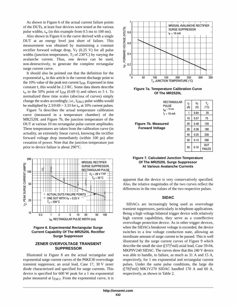
http://onsemi.com432
As shown in Figure 6 of the actual current failure pointsof the DUTs, at least four devices were tested at the variouspulse widths, tw (in this example from 0.5 ms to 100 ms).
Also shown in Figure 6 is the curve derived with a singleDUT at an energy level just short of failure. Thismeasurement was obtained by maintaining a constantrectifier forward voltage drop, VF (0.25 V) for all pulsewidths (junction temperature, TJ of 230°C) by varying theavalanche current. Thus, one device can be used,non-destructively, to generate the complete rectangularsurge current curve.
It should also be pointed out that the definition for theexponential tw in this article is the current discharge point tothe 10% value of the peak test current IZM. Expressed in timeconstant τ, this would be 2.3 RC. Some data sheets describetw to the 50% point of IZM (0.69 τ) and others to 5 τ. Tonormalized these time scales (abscissa of curves) simplychange the scales accordingly; i.e., IZM/2 pulse widths wouldbe multiplied by 2.3/0.69 = 3.33 for tw at 10% current pulses.
Figure 7a describes the actual temperature calibrationcurve (measured in a temperature chamber) of theMR2520L and Figure 7b, the junction temperature of theDUT at various 10 ms rectangular pulse current amplitudes.These temperatures are taken from the calibration curve (inactuality, an extremely linear curve), knowing the rectifierforward voltage drop immediately (within 100 µs) aftercessation of power. Note that the junction temperature justprior to device failure is about 290°C.
Figure 6. Experimental Rectangular SurgeCurrent Capability Of The MR2520L Rectifier
Surge Suppressor
I ,
PE
AK
SU
RG
E C
UR
RE
NT
(AM
PS
)Z
ACTUAL DUTS FAILURE POINTS
ONE DUT WITH VF = 0.25 V
MR2520L RECTIFIER
SURGE SUPPRESSOR,
RECTANGULAR PULSE
VZ = 28 V TYP
TA = 25°C
100
50
20
10
200
10 20 50 1000.5 1 52
tW, RECTANGULAR PULSE WIDTH (ms)
TJ = 230°C
ZENER OVERVOLTAGE TRANSIENTSUPPRESSOR
Illustrated in Figure 8 are the actual rectangular andexponential surge current curves of the P6KE30 overvoltagetransient suppressor, an axial lead, Case 17, 30 V zenerdiode characterized and specified for surge currents. Thisdevice is specified for 600 W peak for a 1 ms exponentialpulse measured at IZM/2. From the exponential curve, it is
Figure 7a. Temperature Calibration CurveOf The MR2520L
V
, FO
RW
AR
D V
OLT
AG
E (
VO
LTS
)F
MR2520L AVALANCHE RECTIFIER
SURGE SUPPRESSOR
IF = 10 mA
0.2
0.6
1
0
0.8
0.4
50 1000 150 200 250 300 350TJ, JUNCTION TEMPERATURE (°C)
RECTANGULAR
PULSE
tW = 10 ms
IF = 10 mA
IZ(A)
VF
(V)
TJ
(°C)
11
10
20
30
40
50
0.64
0.57
0.48
0.36
0.25
0.15
225
75
120
180
230
290
55 0.10DUT
FAILED
Figure 7b. MeasuredForward Voltage
Figure 7. Calculated Junction TemperatureOf The MR2520L Surge Suppressor
At Various Avalanche Currents
apparent that the device is very conservatively specified.Also, the relative magnitudes of the two curves reflect thedifferences in the rms values of the two respective pulses.
SIDAC
SIDACs are increasingly being used as overvoltagetransient suppressors, particularly in telephone applications.Being a high voltage bilateral trigger device with relativelyhigh current capabilities, they serve as a costeffectiveovervoltage protection device. As in other trigger devices,when the SIDACs breakover voltage is exceeded, the deviceswitches to a low voltage conduction state, allowing aninordinate amount of surge current to be passed. This is wellillustrated by the surge current curves of Figure 9 whichdescribe the small die size ([37]2mil) axial lead, Case 59-04,MKP9V240 SIDAC. The curves show that this 240 V devicewas able to handle, to failure, as much as 31 A and 15 A,respectively, for 1 ms exponential and rectangular currentpulses. Under the same pulse conditions, the large die([78]2mil) MK1V270 SIDAC handled 170 A and 60 A,respectively, as shown in Table 2.

http://onsemi.com433
Figure 8. Surge Current Capability Of The P6KE30Overvoltage Transient Suppressor As A Function Of
Exponential & Rectangular Pulse Widths
I ,
PE
AK
SU
RG
E C
UR
RE
NT
(AM
PS
)Z
IZ
10
%tW
RECTANGULAR
EXPONENTIAL
IZ2
@
tW, PULSE WIDTH (ms)
100
50
10
10 50 1000.5 1 50.1 500 1000
P6KE30 OVERVOLTAGE
TRANSIENT SUPPRESSORVZ = 30 V
PSPEC = 600 W pk
5
1
Figure 9. Measured Surge Current To FailureOf A SIDAC MKP9V240
I ,
PE
AK
SU
RG
E C
UR
RE
NT
(AM
PS
)Z
100
50
20
10
10 20 50 1000.2 0.5 1 52
5
1
2
SIDAC MKP9V240240 VCASE 5904372 MILS
EXPONENTIAL
RECTANGULAR
IZ
10
%tW
tW, PULSE WIDTH (ms)
OVERALL RATINGS
The compilation of all of the testing to date on the varioustransient suppressors is shown in Tables 1 and 2. Table 1describes the zener suppressors, avalanche rectifiers andMOVs, comparing the die size and normalized costs(referenced to the MOV V39MA2A). From this data, thedesigner can make a cost/performance judgment.
Of interest is that the small pellet MOV is not the leastexpensive device. The P6KE30 overvoltage transientsuppressor costs about 85% of the MOV, yet it can handleabout three times the current (2.5 A to 0.7 A) for a 100 msrectangular pulse. Under these conditions, the resultantclamping voltages for the zener and MOV were 32 V and60 V respectively.
Also shown in the table is a 1.5 W zener diode specifiedfor zener applications. This low surge current device coststhree times the MOV, illustrating that tight tolerance zenerdiodes are not cost effective and that the user should usedevices designed and priced specifically for the suppressorapplication.
Thyristor type surge suppressors are shown in Table 2.They include four SIDAC series, two SCRs designed andcharacterized specifically for crowbar applications and alsothe MOS SCR MCR1000. The MOS SCR, a processvariation of the vertical structure power MOSFET,combines the input characteristics of the FET with thelatching action of an SCR.
All devices were surge current tested with the resultantpeak currents being impressively high. The TO-220 (150)2
mil SCR MCR69 for example, reached peak current levelsapproaching 700 A for a 1 ms exponential pulse. Theguaranteed, derated, time base translated curves for thecrowbar SCR family of devices are shown in Figure 10, asis the MK1V SIDAC in Figure 11.
Figures 12A–C describe the guaranteed, reverse surgedesign limits for the avalanche rectifier devices. These threefigures illustrate, respectively, the peak current, power andenergy capabilities of these overvoltage transientsuppressors derived from exponential testing. The peakpower, Ppk, ordinate of the curve is simply the product of thederated IZ and VZ and the energy curve, the product of Ppkand tw.

http://onsemi.com434
Figure 10. SCR Crowbar Derating Curves
Figure 11. Exponential Surge CurrentCapability Of The MK1V SIDAC, Pulse Width
versus Peak Current
Figure 12b. Peak Power
Ipk
5 TCtW
I ,
PE
AK
CU
RR
EN
T (A
MP
S)
pkC = 8400 µF TA = 25°C
ESR ≈ 25 mΩ N = 2000 PULSES
VC ≤ 60 V f = 3 PULSES/MIN.
a. Peak Surge Current versus Pulse Width
MCR70
MCR69MCR68
MCR67
MCR71
100
30
3000
1000
300
0.5 1 50.1 5010 100
tW, BASE PULSE WIDTH (ms)
SIDAC MK1V115
V(BO) = 115 V MAX
TA = 25°C
tW, PULSE WIDTH (ms)
I ,
PE
AK
SU
RG
E C
UR
RE
NT
(AM
PS
)Z
100
50
30
10
1
3
5
10 30 50 1000.3 0.5 1 3 5 300
IZ
10%
tW
TC = 25°C, DUTY CYCLE ≤ 1%
SEE NOTE FOR TIME
CONSTANT DEFINITION
MR2530L
MR2525L
MR2520L
, PE
AK
RE
VE
RS
E P
OW
ER
(W
AT
TS
)R
SM
P 700
500
7000
5000
3000
2000
1000
10 20 50 1001 52 200 500 1000τ, TIME CONSTANT (ms)
10000
b. Peak Surge Current versusAmbient Temperature
25 7550 1000 125
0.6
0.8
1
0.4
NO
RM
ALI
ZE
D P
EA
K S
UR
GE
CU
RR
EN
T
N = 2000 PULSES
Figure 12a. Peak Current
TC = 25°C, DUTY CYCLE ≤ 1%
SEE NOTE FOR TIME
CONSTANT DEFINITION
MR2530L
MR2525L
MR2520L
200
70
50
20
300
100
30, PE
AK
RE
VE
RS
E C
UR
RE
NT
(AM
PS
)R
SM
I
10 20 50 1001 52 200 500 1000
τ, TIME CONSTANT (ms)
TC = 25°C, DUTY CYCLE ≤ 1%
SEE NOTE FOR TIME
CONSTANT DEFINITION
MR2530L
MR2525L
MR2520L
τ, TIME CONSTANT (ms)
100
50
20
30
200
300
, PE
AK
RE
VE
RS
E E
NE
RG
Y (
JOU
LES
)R
SM
W
10 20 50 1001 52 200 500 1000
Figure 12c. Energy
Figure 12. Guaranteed Reverse Surge Design Limits for theMR2525L & MR2530L Overload Transient Suppressors
TA, AMBIENT TEMPERATURE (°C)
NOTE: τ = RC

http://onsemi.com435
Table 1. Measured Surge Current Capability of Transient Suppressors
Spec. Peak Current at Pulse Widths, Ipk (Amps)Clamping
Device Power Die1 ms 10 ms 20 ms 100 ms
ClampingFactorV1 ms
Norm.
CostDevice
Type Title Part No. Case VoltPower
(Energy)
Die
Size Exp. Rect. Exp. Rect. Exp. Rect. Exp. Rect.
V1msV100ms
Cost
*
Avalanche
Surge Supp.,
OvervoltageMR2520L
194 05
24-32 V2.5KW
Peak
1502
mil85 A 40 30 18 27V
22V 1.2
Avalanche
Rectifier
Overvoltage
Transient
Suppressor MR2525L
194-05
24-32 V10KW
Peak
1962
mil150 A 70 54 37 31
23 1.3 4.0
1.5 W Zener1N5936A
DO 41
30 V1.5 W 372
12 A 5 6 2.5 5 2 3 1.3 4130
1.4
3 21.5 W Zener
Diode1N5932A
DO-41
20 V
1.5 W
Cont.
37
mil23 A 6 10 2.8 7 2.3 5 1.4 28
23 1.2
3.2
Zener
Overvoltage
Transient
P6KE30
17
30 V600 W 602
43 A 14 14 5 10 4.5 5 2.5 4132
1.3
0 85Zener Transient
Suppressor P6KE10
17
10 V
600 W
Peak
60
mil24 A 12 9 5.5 16
13 1.2
0.85
MOSORB
1.5KE30
41A 02
30 V1500 W 1042
35 A 10 4 3533
1.1
1 8MOSORB
1.5KE24
41A-02
24 V
1500 W
Peak
104
mil45 A 14 6 30V
28V 1.1
1.8
MOV**
Metal
Oxide
V39MA2AAxial
Lead28 V 0.16
Joules 3 mm 9 A 5 0.780V
60V
6A
0.7A1.0
MOV** Oxide
Varistor V33ZA1Radial
Lead26 V 1.0
Joules 7 mm 35 4 A105V
80V
35A
4A1.4
**G.E.
Table 2. Measured Surge Current Of Thyristor Type Devices
Ipk @ tW
Voltage Die1 ms 10 ms Norm
CostTechnology Device
VoltageRatings Case
DieSize Exponent. Rectang. Exponent. Rectang.
Cost*
MKP9V130 Series 104 V–135 V59 04 372 mil
40 A 13 A 16 A 8 A0 87
SIDACMKP9V240 Series 220 V–280 V
59–04 372 mil31 A 15 A 20 A 8 A
0.87
SIDACMK1V135 Series 120 V–135 V
267 01 782 mil140 A 80 A 55 A 30 A
1 1MK1V270 Series 220 V–280 V
267–01 782 mil170 A 60 A 90 A 28 A
1.1
SCRMCR68 Series
25 V 400 V922 mil 300 A 170 A 1.2
SCRMCR69 Series
25 V–400 V
TO 2201502 mil 700 A 400 A 1.9
MOS SCR MCR1000 Series 200 V–600 V
TO–220127 mil
x183 mil
250 A 170 A 9.3
*Normalized to G.E. MOV V39MA2A, Qty 1-99, 1984 Price
Additionally, the published non-repetitive peak powerratings of the various zener diode packages are illustrated inFigure 13. Figure 14 describes the typical derating factor forrepetitive conditions of duty cycles up to 20%. Using thesetwo empirically derived curves, the designer can thendetermine the proper zener for the repetitive peak currentconditions.
At first glance the derating of curves of Figure 14 appearto be in error as the 10 ms pulse has a higher derating factorthan the 10 µs pulse. However, when the mathematics ofmultiplying the derating factor of Figure 14 by the peakpower value of Figure 13 is performed, the resultantrespective power and current capability of the devicefollows the expected trend. For example, for a 5 W, 20 V
zener operating at a 1.0% duty cycle, the respective deratingfactors for 10 µs and 10 ms pulses are 0.08 and 0.47. Thenon-repetitive peak power capabilities for these two pulses(10 µs and 10 ms) are about 1300 W and 50 W respectively,resulting in repetitive power and current capabilities ofabout 104 W and 24 W and consequently 5.2 A and 1.2 A.
MOV
All of the surge suppressors tested with the exception ofthe MOV are semiconductors. The MOV is fabricated froma ceramic (Zn0), non-linear resistor. This device has wideacceptance for a number of reasons, but for manyapplications, particularly those requiring good clamping

http://onsemi.com436
Figure 13. Peak Power Ratings of Zener Diodes
Power is defined as VZ(NOM) x IZ(PK) where VZ(NOM) is thenominal zener voltage measured at the low test current used forvoltage classification.
1N6267 SERIES
GLASS DO35 & GLASS DO41250 mW TO 1 W TYPES
5 WATT TYPES
PULSE WIDTH (ms)
0.1
100
0.01 0.02
PP
K(N
OM
), N
OM
INA
L P
EA
K P
OW
ER
(kW
)50
20
10
5
2
1
0.5
0.2
0.1
0.05
0.02
0.010.05 0.2 0.5 1 2 5 10
1 TO 3 W TYPESPLASTIC DO41
Figure 14. Typical Derating Factor for Duty Cycle
0.1 0.2 0.5 1 52 10 20 50 100
PULSE WIDTH10 ms
1 ms
100 µs
10 µs
D, DUTY CYCLE (%)
DE
RAT
ING
FA
CT
OR
1
0.70.5
0.3
0.2
0.02
0.1
0.070.05
0.03
0.01
factors, the MOV is found lacking; (clamping factor isdefined as the ratio of VZ at the test current to that at 1.0 mA).This is photographically illustrated in Figure 15 whichcompares a 27 V zener (1N6281) with a 27 V MOV(V27ZA4). The input waveform, through a sourceimpedance resistance to the DUTs, was an exponentiallydecaying voltage waveform of 90 V peak. Figures 15A andB compare the output waveforms (across the DUTs) whenthe source impedance was 500 Ω and Figures 15C and D fora 50 Ω condition. The zener clamped at about 27 V for bothimpedances whereas the MOV was about 40 V and 45 Vrespectively.
Surge current capabilities of a comparably powered MOVwere also determined, as shown in the curve of Figure 16.Although the MOV, a V39MA2A, is specified as a 28 V
Figure 15a.
Figure 15b.
SOURCE IMPEDANCE RS = 500 Ω
27 V MOV
G.E. V27ZA4, 4 JOULES CAPABILITY
27 V ZENER DIODE
ON Semiconductor 1N6281, APPROX. 1.5 JOULES
SOURCE IMPEDANCE RS = 500 Ω
continuous device (39 V ±10% at 1 mA) at the pulse widthsand currents tested, the resultant voltage VZ across the MOV– 80 V at about 6 A – necessitated a high voltage fixture. Thiswas accomplished with a circuit similar to that of Figure 1B.
But MOVs do have their own niche in the marketplace, asdescribed in Table 3, the Relative Features of MOVs andMOSORBs.

http://onsemi.com437
Figure 15c.
Figure 15d.
27 V MOV
27 V ZENER DIODE
Figure 15. Clamping Characteristics of a27 V Zener Diode and 27 V MOV
SOURCE IMPEDANCE RS = 50 Ω
SOURCE IMPEDANCE RS = 50 Ω
G.E. V39MA2A MOV
VDCM = 28 V
VNOM = 39 V @ 1 mA
TA = 25°C
10
5
0.3
0.5
3
0.1
1
10 30 50 1001 3 5
I ,
PE
AK
SU
RG
E C
UR
RE
NT
(AM
PS
)Z
tW, PULSE WIDTH (ms)
Figure 16. Rectangular Surge Current CapabilityOf The V39MA2A MOV
Table 3. Relative Features of MOVsand MOSORBs
MOVMOSORB/Zener Transient
Suppressor
High Clamping Factor Very good clamping close tothe operating voltage.
Symmetrically bidirectional Standard parts perform likestandard zeners. Symmetricalbidirectional devices availablefor many voltages.
Energy capability per dollarusually much greater than asilicon device. However, ifgood clamping is required ahigher energy device would beneeded, resulting in highercost.
Good clampingcharacteristics could reduceoverall cost.
Inherent wear out mechanism,clamp voltage degrades afterevery pulse, even whenpulsed below rated value.
No inherent wear outmechanism.
Ideally suited for crude AC lineprotection.
Ideally suited for precise DCprotection.
High single-pulse currentcapability.
Medium multiple-pulsecurrent capability.
Degrades with overstress. Fails short with overstress.
Good high voltage capability. Limited high voltage capabilityunless series devices areused.
Limited low voltage capability. Good low voltage capability.

http://onsemi.com438
SUMMARY
The surge current capabilities of low energy overvoltagetransient suppressors have been demonstrated, includingcost/performance comparison of rectifiers, zeners, thyristortype suppressors, and MOVs. Both rectangular andexponential testing have been performed with the describedtesters. Additionally, the Rectangular Current Surge Testerhas the capability of measuring the diode junctiontemperature of zeners and rectifiers at various power levels,thus establishing safe operating limits.
REFERENCES
1. Cherniak, S., A Review of Transients and Their Meansof Suppression, ON Semiconductor Application NoteAN843.
2. Wilhardt, J., Transient Power Capability of ZenerDiodes, ON Semiconductor Application Note AN784.
3. Pshanenich, A., Characterizing the SCR for CrowbarApplications, ON Semiconductor Application NoteAN879.
4. Pshaenich, A., The SIDAC, A New High VoltageTrigger that Replaces Circuit Complexity and Cost,ON Semiconductor Engineering Bulletin EB-106.
5. General Electric, Transient Voltage SuppressionManual, Second Edition.

http://onsemi.com439
MEASUREMENT OF ZENER VOLTAGE TO THERMAL EQUILIBRIUMWITH PULSED TEST CURRENT
Prepared byHerb SaladinDiscrete Power Application Engineering
INTRODUCTION
This paper discusses the zener voltage correlationproblem which sometimes exists between the manufacturerand the customer’s incoming inspection. A method is shownto aid in the correlation of zener voltage between thermalequilibrium and pulse testing. A unique double pulsedsample and hold test circuit is presented which improves theaccuracy of correlation.1
Several zener voltages versus zener pulsed test currentcurves are shown for four package styles. An appendix isattached for incoming inspection groups giving detailedinformation on tolerances involved in correlation.
For many years the major difficulty with zener diodetesting seemed to be correlation of tight tolerance voltagespecifications where accuracy between different test setupswas the main problem. The industry standard and the EIARegistration system adopted thermal equilibrium testing ofzener diodes as the basic test condition unless otherwisespecified. Thermal equilibrium was chosen because it wasthe most common condition in the final circuit design and itwas the condition that the design engineers needed for theircircuit design and device selection. Thermal equilibriumtesting was also fairly simple to set-up for sample testing atincoming inspection of standard tolerance zeners.
In recent years with the advent of economicalcomputerized test systems many incoming inspection areashave implemented computer testing of zener diodes whichhas been generating a new wave of correlation problemsbetween customers and suppliers of zener diodes.
The computerized test system uses short duration pulsetest techniques for testing zener diodes which does notdirectly match the industry standard thermal equilibriumtest specifications.
This paper was prepared in an attempt to clarify thedifferences between thermal equilibrium and short durationpulse testing of zener diodes, to provide a test circuit thatallows evaluation at various pulse widths and a suggestedprocedure for incoming inspection areas that will allowmeaningful correlation between thermal equilibrium andpulse testing.
In the measurement of zener voltage (VZ), thetemperature coefficient effect combined with test currentheating can present a problem if one is attempting tocorrelate VZ measurements made by another party (FinalTest, Quality Assurance or Incoming Inspection).2 Thispaper is intended as an aid in determining VZ at some test
current (IZT) pulse width other than the pulse width used bythe manufacturer.
Thermal equilibrium (TE) is reached when diode junctiontemperature has stabilized and no further change will occurin VZ if the IZT time is increased.2 This absolute value canvary depending on the mounting method and amount ofheatsinking. Therefore, thermal equilibrium conditionshave to be defined before meaningful correlation can exist.
Normalized VZ curves are shown for four package stylesand for three to five voltage ratings per package. Pulsewidths from 1 ms up to 100 seconds were used to arrive ator near thermal equilibrium for all packages with a givenmethod of mounting.
Mounting
There are five conditions that can affect the correlation ofVZ measurements and are: 1) instrumentation, 2) TA, 3) IZTtime, 4) PD and 5) mounting. The importance of the firstfour conditions is obvious but the last one, mounting, canmake the difference between good and poor correlation. Themounting can have a very important part in VZ correlationas it controls the amount of heat and rate of heat removalfrom the diode by the mass and material in contact with thediode package.
Two glass axial lead packages (DO-35 and DO-41),curves (Figures 5 and 6) were measured with standardGrayhill clips and a modified version of the Grayhill clips topermit lead length adjustment.
Test Circuit
The test circuit (Figure 8) consists of standard CMOSlogic for pulse generation, inverting and delaying. The logicdrives three bipolar transistors for generation of the powerpulse for IZT. VZ is fed into an unique sample and hold (S/H)circuit consisting of two high input impedance operationalamplifiers and a field effect transistor switch.
For greater accuracy in VZ measurements using a singlepulse test current, the FET switch is double pulsed. Doublepulsing the FET switch for charging the S/H capacitorincreases accuracy of the charge on the capacitor as thesecond pulse permits charging the capacitor closer to thefinal value of VZ.
The timing required for the two pulse system is shown inwaveform G-3C whereby the initial sample pulse is delayedfrom time zero by a fixed 100 µs to allow settling time andthe second pulse is variable in time to measure the analoginput at that particular point. The power pulse (waveformG-2D) must also encompass the second sample pulse.

http://onsemi.com440
To generate these waveforms, four time delay monostablemultivibrators (MV) are required. Also, an astable MV, isrequired for free-running operation; single pulsing is simplyinitiated by a push-button switch S1. All of the pulsegenerators are fashioned from two input, CMOS NOR gates;thus three quad gate packages (MC14001) are required.Gates 1A and 1B form a classical CMOS astable MV clockand the other gates (with the exception of Gate 2D) comprisethe two input NOR gate configured monostable MV’s. ThePulse Width variable delay output (Gate 1D) positions thesecond sample pulse and also triggers the 100 µs Delay MVand the 200 µs Extended Power Pulse MV, The respectivepositive going outputs from gates 3A and 2C are diodeNOR’ed to trigger the Sample Gate MV whose output willconsequently be the two sample pulses. These pulses thenturn on the PNP transistor Q1 level translator and thefollowing S/H N-channel FET series switch Q2. Op ampsU4 and U5, configured as voltage followers, respectivelyprovide the buffered low output impedance drive for theinput and output of the S/H. Finally, the pulse extendedPower Gate is derived by NORing (Gate 2D) the PulseWidth Output (Gate 1D) with the 200 µs MV output (Gate2C). This negative aging gate then drives the PowerAmplifier, which, in turn, powers the D.U.T. The poweramplifier configuration consists of cascaded transistorsQ3–Q5, scaled for test currents up to 2 A.
Push button switch (S4) is used to discharge the S/Hcapacitor. To adjust the zero control potentiometer, groundthe non-inverting input (Pin 3) of U4 and discharge the S/Hcapacitor.
Testing
The voltage VCC, should be about 50 volts higher than theD.U.T. and with RC selected to limit the IZT pulse to a valuemaking VZT IZT = 1/4 PD (max), thus insuring a good currentsource. All testing was performed at a normal roomtemperature of 25°C. A single pulse (manual) was used andat a low enough rate that very little heat remained from theprevious pulse.
The pulse width MV (1C and 1D) controls the width of thetest pulse with a selector switch S3 (see Table 1 for capacitorvalues). Fixed widths in steps of 1, 3 and 5 from 1 ms to 10seconds in either a repetitive mode or single pulse isavailable. For pulse widths greater than 10 seconds, a stopwatch was used with push button switch (S1) and with themode switch (S2) in the > 10 seconds position.
For all diodes with VZ greater than about 6 volts a resistorvoltage divider is used to maintain an input of about 6 V tothe first op amp (U4) so as not to overload or saturate thisdevice. The divider consists of R5 and R6 with R6 being10 kΩ and R5 is selected for about a 6 V input to U4.Precision resistors or accurate known values are required foraccurate voltage readout.
Table 1. S3 — Pulse Width
SwitchPosition *C(µF) t(ms)
12345678910111213
0.0010.0040.0060.010.040.060.10.40.61.01.26.010
1351030501003005001K3K5K10K
*Approximate Values
Using Curves
Normalized VZ versus IZT pulse width curves are shownin Figure 1 through 6. The type of heatsink used is shown orspecified for each device package type. Obviously, it isbeyond the scope of this paper to show curves for everyvoltage rating available for each package type. The objectwas to have a representative showing of voltages includingwhen available, one diode with a negative temperaturecoefficient (TC).
These curves are actually a plot of thermal responseversus time at one quarter of the rated power dissipation.With a given heatsink mounting, VZ can be calculated atsome pulse width other than the pulse width used to specifyVZ.
For example, refer to Figure 5 which shows normalizedVZ curves for the axial lead DO-35 glass package. Threemounting methods are shown to show how the mountingeffects device heating and thus VZ. Curves are shown for a3.9 V diode (1N5228B) which has a negative TC and a 12 Vdiode (1N5242B) having a positive TC.
In Figure 5, the two curves generated using the Grayhillmountings are normalized to VZ at TE using theON Semiconductor fixture. There is very little difference inVZ at pulse widths up to about 10 seconds and mounting onlycauses a very small error in VZ. The maximum error occursat TE between mountings and can be excessive if VZ isspecified at TE and a customer measures VZ at some narrowpulse width and does not use a correction factor.
Using the curves of Figure 5, VZ can be calculated at anypulse width based upon the value of VZ at TE which isrepresented by 1 on the normalized VZ scale. If the 1N5242Bdiode is specified at 12 V ± 1.0% at 90 seconds which is atTE, VZ at 100 ms using either of the Grayhill clips curveswould be 0.984 of the VZ value at TE or 1 using theON Semiconductor fixture curve. If the negative TC diodeis specified at 3.9 V ± 1.0% at TE (90 seconds), VZ at 100ms would be 1.011 of VZ at TE (using ON Semiconductorfixture curve) when using the Grayhill Clips curves.

http://onsemi.com441
In using the curves of Figure 5 and 6, it should be kept inmind that VZ can be different at TE for the three mountingsbecause diode junction temperature can be different for eachmounting at TE which is represented by 1 on the VZnormalized scale. Therefore, when the correlation of VZbetween parties is attempted, they must use the same type ofmounting or know what the delta VZ is between the twomountings involved.
The Grayhill clips curves in Figure 6 are normalized to theON Semiconductor fixture at TE as in Figure 5. Figures 1through 4 are normalized to VZ at TE for each diode andwould be used as Figures 5 and 6.
Measurement accuracy can be affected by test equipment,power dissipation of the D.U.T., ambient temperature andaccuracy of the voltage divider if used on the input of the firstop-amp (U4). The curves of Figures 1 through 6 are for anambient temperature of 25°C, at other ambients, θVZ has tobe considered and is shown on the data sheet for the1N5221B series of diodes. θVZ is expressed in mV/°C andfor the 1N5228B diode is about –2 mV/°C and for the1N5242B, about 1.6 mV/°C. These values are multiplied bythe difference in TA from the 25°C value and either
subtracted or added to the calculated VZ depending uponwhether the diode has a negative or positive TC.
General Discussion
The TC of zener diodes can be either negative or positive,depending upon die processing. Generally, devices with abreakdown voltage greater than about 5 V have a positiveTC and diodes under about 5 V have a negative TC.
Conclusion
Curves showing VZ versus IZT pulse width can be used tocalculate VZ at a pulse width other than the one used tospecify VZ. A test circuit and method is presented to obtainVZ with a single pulse of test current to generate VZ curvesof interest.
References
1. Al Pshaenich, “Double Pulsing S/H Increases SystemAccuracy”; Electronics, June 16, 1983.
2. ON Semiconductor Zener Diode Manual, Series A,1980.

http://onsemi.com442
FIGURES 1 thru 8 — Conditions: Single Pulse, TA = 25°C, VZ IZT = 1/4 PD (Max) Each device normalized to VZ at TE.
AXIAL LEAD PACKAGES: MOUNTING STANDARD GRAYHILL CLIPS
Figure 1. DO-35 (Glass) 500 mW Device Figure 2. DO-41 (Glass) 1 Watt Device
Figure 3. DO-41 (Plastic) 1.5 Watt Device Figure 4. Case 17 (Plastic) 5 Watt Device
V
, ZE
NE
R V
OLT
AG
E (
NO
RM
ALI
ZE
D)
Z
VZ = 3.9 V
6.2 V
12 V
1.06
1.04
1.02
1
0.98
0.96
0.94
0.9210 40 1001 4 400 1K 4K 10K 40K 100K
PW, PULSE WIDTH (ms)
75 V
1.06
1.04
1.02
1
0.98
0.96
0.94
0.92
V
, ZE
NE
R V
OLT
AG
E (
NO
RM
ALI
ZE
D)
Z
10 40 1001 4 400 1K 4K 10K 40K100K
PW, PULSE WIDTH (ms)
VZ = 3.9 V
6.2 V
12 V
V
, ZE
NE
R V
OLT
AG
E (
NO
RM
ALI
ZE
D)
Z
VZ = 3.3 V
6.2 V
12 V
1.06
1.04
1.02
1
0.98
0.96
0.94
0.9210 40 1001 4 400 1K 4K 10K 40K 100K
PW, PULSE WIDTH (ms)
V
, ZE
NE
R V
OLT
AG
E (
NO
RM
ALI
ZE
D)
Z
VZ = 3.9 V
6 V
13 V
1.06
1.04
1.02
1
0.98
0.96
0.94
0.9210 40 1001 4 400 1K 4K 10K 40K100K
PW, PULSE WIDTH (ms)
68 V 150 V

http://onsemi.com443
THREE MOUNTING METHODS: DO-35 AND DO-41
Figure 5. DO-35 (Glass) 500 mW Device
Figure 6. DO-41 (Glass) 1 Watt Device
Figure 7. Standard Grayhill Clips
MOUNTING FIXTURE
1N5242B (VZ = 12 V)
1N5228B (VZ = 3.9 V)
GRAYHILL CLIPSSTANDARD, L = 11/16″
ON SEMICONDUCTORFIXTURE L = 1/2″
MOUNTINGS:
MODIFIEDL = 3/8″
1.022
1.018
1.014
1.012
1.008
1.004
1
0.996
10 40 1001 4 400 1K 4K 10K 40K 100K
0.992
0.988
0.984
0.98
0.976
0.972
0.968
V
, ZE
NE
R V
OLT
AG
E (
NO
RM
ALI
ZE
D)
Z
PW, PULSE WIDTH (ms)
1.004
1
10 40 1001 400 1K 4K 10K 40K 100K
0.992
0.988
0.984
0.98
0.9764
0.996
MOUNTINGS:GRAYHILL CLIPS
STANDARD, L = 11/16″MODIFIED, L = 3/8″
ON SEMICONDUCTORFIXTUREL = 1/2″
1N4742A
VZ = 12 V
V
, ZE
NE
R V
OLT
AG
E (
NO
RM
ALI
ZE
D)
Z
PW, PULSE WIDTH (ms)
1.41
1.69
.78
.75
2.31
GRAYHILL CLIPSMODIFIED, L = 3/8″
STANDARD,L = 11/16″

http://onsemi.com444
Figure 8. Zener Voltage Double Pulsing S/H Test Circuit
3B
3D3C
2C
1D
0.1
+12
V
1A1B
1C
2A2B
3A
2D
100
100
k22
pF
1N91
4
1/2
MC
1400
1U
312
k
22 k
4.7
k
10 k
12 k
1 k
Q4
MP
SA
42
PO
WE
R A
MP
LIF
ER
RC
R5
68 k
2 W
DU
T
**
Q5A
*M
JE35
0
R6
10 k
1N91
4
U4
MC
1741
VIN
+ - -12
V0.
1 µF
2N48
56
SD
Q2
0.1
µF
S4
0.1
µF
-12
V
0.1
µF0.1
µF
VO
=V
INK
ZE
RO
CO
NT
RO
L+
12 V
25 k
VIN
=V
IN (
10 k
)
R5
+ 10
k
VIN K
=
+12
VV
CC
≤ 2
50 V
1N91
433
pF
-12
V10 k
22 k
47 k
Q1
2N39
06
+12
V
SA
MP
LE G
AT
E M
V51
0 pF
330
k
U3
1/2
MC
1400
1
+12
V
EX
TE
ND
ED
PO
WE
RP
ULS
E M
V
1N91
4
47 k
47 k
0.00
1µF
47 k1N
914
0.00
1 µF
200
µs
+12
V 680
k
510
pF
27 k
+12
VU
33/
4 M
C14
001
0.00
1 µF
VD
D
510
pF
330
k
+12
V
VD
D
+12
V
0.00
1 µF
27 k
100
µsD
ELA
Y M
V
1/4
MC
1400
1U
2
S2B
≈2 R
1R
1
C1
VD
D
T1
≈ 2.
2R1C
1
MC
1400
1
1N91
4
MO
DE
SE
L S
WS
2A
10 k
ON
ES
HO
T
0.00
1 µF
>10
SE
C
STA
RT
SW
S1
+12
V
+12
V
100
k
FR
EE
RU
N
C2
C4
C5
C15C3
100
kR
2
5M R3
P.W
.C
ON
TR
OL
T2
≈ 0.
6C2
(R2
+ R
3)
1
S3
SE
ETA
BLE
1
PU
LSE
WID
TH
MV
2 3 13
27 k
TIM
ING
WA
VE
FO
RM
S
GA
TE
G1
D
G2
A
G2
C
G2
D
G3
A G3
C
100
µs
100
µs10
0 µs20
0 µs
2N 3906
Q3
+ -
+12
V+1
2 V
U5
LF15
5J
**Te
k C
urre
nt P
robe
**P
6302
/AM
503
1 k
12 k
68 k
2 W
RC
Q4
*FO
R D
UT
CU
RR
EN
TS
:20
0 m
A ≤
I ZT ≤
2 A
VC
C ≤
250
V
DU
T
Q5A
MJE
35
Q5B
MJE
5850
VC
C ≤
250
V

http://onsemi.com445
APPENDIX ARecommended Incoming Inspection Procedures
Zener Voltage TestingPulsed versus Thermal Equilibrium
This section is primarily for use of incoming inspectiongroups. The subject covered is the measurement of zenervoltage (VZ) and the inherent difficulty of establishingcorrelation between supplier and buyer when using pulsedtest techniques. This difficulty, in part, is due to theinterpretation of the data taken from the variety of availabletesters and in some cases even from the same model types.It is therefore, our intent to define and reestablish astandardized method of measurement to achieve correlationno matter what test techniques are being used. Thisstandardization will guarantee your acceptance of goodproduct while maintaining reliable correlation.
DEFINITION OF TERMS
Temperature Coefficient (TC):
The temperature stability of zener voltages is sometimesexpressed by means of the temperature coefficient (TC).This parameter is usually defined as the percent voltagechange across the device per degree centigrade, or as aspecific voltage change per degree centigrade. Temperaturechanges during test are due to the self heating effects causedby the dissipation of power in the zener junction. The VZ willchange due to this temperature change and will exhibit apositive or negative TC, depending on the zener voltage.Generally, devices with a zener voltage below five volts willhave a negative TC and devices above five volts will exhibita positive TC.
Thermal Equilibrium (TE)
Thermal equilibrium (TE) is reached when the diodejunction temperature has stabilized and no further changewill occur. In thermal equilibrium, the heat generated at thejunction is removed as rapidly as it is created, hence, nofurther temperature changes.
MEASURING ZENER VOLTAGE
The zener voltage, being a temperature dependentparameter, needs to be controlled for valid VZ correlation.Therefore, so that a common base of comparison can beestablished, a reliable measure of VZ can only occur whenall possible variables are held constant. This common baseis achieved when the device under test has had sufficienttime to reach thermal equilibrium (heatsinking is required tostabilize the lead or case temperature to a specified value for
stable junction temperatures). The device should also bepowered from a constant current source to limit changes ofpower dissipated and impedance.
All of the above leads us to an understanding of whyvarious pulse testers will give differing VZ readings; thesedifferences are, in part, due to the time duration of test (pulsewidth), duty cycle when data logging, contact resistance,tolerance, temperature, etc. To resolve all of this, one onlyneeds a reference standard to compare their pulsed resultsagainst and then adjust their limits to reflect thosedifferences. It should be noted that in a large percentage ofapplications the zener diode is used in thermal equilibrium.
ON Semiconductor guarantees all of it’s axial leadedzener products (unless otherwise specified) to be withinspecification ninety (90) seconds after the application ofpower while holding the lead temperatures at 30 ± 1°C, 3/8of an inch from the device body, any fixture that will meetthat criteria will correlate. 30°C was selected over thenormally specified 25°C because of its ease of maintenance(no environmental chambers required) in a normal roomambient. A few degrees variation should have negligibleeffect in most cases. Hence, a moderate to large heatsink inmost room ambients should suffice.
Also, it is advisable to limit extraneous air movementsacross the device under test as this could change thermalequilibrium enough to affect correlation.
SETTING PULSED TESTER LIMITS
Pulsed test techniques do not allow a sufficient time forzener junctions to reach TE. Hence, the limits need to be setat different values to reflect the VZ at lower junctiontemperatures. Since there are many varieties of test systemsand possible heatsinks, the way to establish these limits is toactually measure both TE and pulsed VZ on a serializedsample for correlation.
The following examples show typical delta changes inpulsed versus TE readings. The actual values you use forpulsed conditions will depend on your tester. Note, that thereare examples for both positive and negative temperaturecoefficients. When setting the computer limits for a positiveTC device, the largest difference is subtracted from theupper limit and the smallest difference is subtracted from thelower limit. In the negative coefficient example the largestchange is added to the lower limit and the smallest changeis added to the upper limit.

http://onsemi.com446
ON Semiconductor Zeners
• Thermal equilibrium specifications:VZ at 10 mA, 9 V minimum, 11 V maximum:(Positive TC)
TE Pulsed Difference
9.53 V9.35 V9.46 V9.56 V9.50 V
9.45 V9.38 V9.83 V9.49 V9.40 V
–0.08 V–0.07 V–0.08 V–0.07 V–0.10 V
Computer test limits:Set VZ max. limit at 11 V – 0.10 V = 10.9 VSet VZ min. limit at 9 V – 0.07 V = 8.93 V
• Thermal equilibrium specifications:VZ at 10 mA, 2.7 V minimum, 3.3 V maximum:(Negative TC)
TE Pulsed Difference
2.78 V2.84 V2.78 V2.86 V2.82 V
2.83 V2.91 V2.84 V2.93 V2.87 V
+0.05 V+0.07 V+0.05 V+0.07 V+0.05 V
Computer test limits:Set VZ min. limit at 2.7 V + 0.07 V = 2.77 VSet VZ max. limit at 3.3 V + 0.05 V = 3.35 V

http://onsemi.com447
ON SEMICONDUCTOR MAJOR WORLDWIDE SALES OFFICESUNITED STATES
ALABAMAHuntsville 256–774–1000. . . . . . . . . . . . . . . . . .
CALIFORNIAIrvine 949–623–8485. . . . . . . . . . . . . . . . . . . . . . San Jose 408–350–4800. . . . . . . . . . . . . . . . . . Encino 818–654–9040. . . . . . . . . . . . . . . . . . . . .
COLORADOLittleton 303–256–5884. . . . . . . . . . . . . . . . . . . .
FLORIDATampa 813–286–6181. . . . . . . . . . . . . . . . . . . . .
GEORGIAAtlanta 888–793–3435. . . . . . . . . . . . . . . . . . . .
ILLINOISChicago 847–413–2500. . . . . . . . . . . . . . . . . . .
INDIANACarmel 317–848–9958. . . . . . . . . . . . . . . . . . . .
MASSACHUSETTSBoston 781–376–4223. . . . . . . . . . . . . . . . . . . .
MICHIGANDetroit 734–953–6704. . . . . . . . . . . . . . . . . . . . .
MINNESOTAPlymouth 763–249–2360. . . . . . . . . . . . . . . . . .
NORTH CAROLINARaleigh 919–785–5025. . . . . . . . . . . . . . . . . . . .
PENNSYLVANIAPhiladelphia/Horsham 215–997–4340. . . . . . .
TEXASDallas 972–633–0881. . . . . . . . . . . . . . . . . . . . .
UTAHDraper 801–572–4010. . . . . . . . . . . . . . . . . . . . .
CANADA
ONTARIOOttawa 613–226–3491. . . . . . . . . . . . . . . . . . . .
QUEBECSt. Laurent 514–333–2125. . . . . . . . . . . . . . . . .
INTERNATIONAL
BRAZILSao Paulo 55–011–3030–5244. . . . . . . . . . . . .
CHINABeijing 86–10–8518–2323. . . . . . . . . . . . . . . . . Chengdu 86–28–678–4078. . . . . . . . . . . . . . . . . Shenzhen 86–755–209–1128. . . . . . . . . . . . . . . Shanghai 86–21–6875–6677. . . . . . . . . . . . . .
CZECH REPUBLICRoznov 420 (0) 651–667–141. . . . . . . . . . . . . .
FINLANDVantaa 358 (0) 9–85–666–460. . . . . . . . . . . . .
FRANCEParis 33 (0) 1–39–26–41–00. . . . . . . . . . . . . . .
GERMANYMunich 49 (0) 89–93–0808–0. . . . . . . . . . . . . .
HONG KONGHong Kong 852–2689–0088. . . . . . . . . . . . . . . .
INDIABangalore 91–80–226–7272 x239. . . . . . . . . .
ISRAELHerzelia 972 (0) 9–9609–111. . . . . . . . . . . . . .
INTERNATIONAL (continued)
ITALYMilan 39 (0) 2–530–0951. . . . . . . . . . . . . . . . . .
JAPANTokyo 81–3–5740–2700. . . . . . . . . . . . . . . . . . .
KOREASeoul 82–2–528–2700. . . . . . . . . . . . . . . . . . . . .
MALAYSIAPenang 60–4–226–9368. . . . . . . . . . . . . . . . . . .
MEXICOGuadalajara 523–669–9100. . . . . . . . . . . . . . . .
PHILIPPINESMuntinlupa City 63–2–842–7141. . . . . . . . . . . .
PUERTO RICOSan Juan 787–641–4100. . . . . . . . . . . . . . . . . .
SINGAPORESingapore 65–298–1768. . . . . . . . . . . . . . . . . . .
SPAINMadrid 34–91–745–6817. . . . . . . . . . . . . . . . . . .
SWEDENSolna 46 (0) 8–5090–4680. . . . . . . . . . . . . . . . .
TAIWANTaipei 886–2–2718–9961. . . . . . . . . . . . . . . . .
THAILANDBangkok 66–2–653–5031. . . . . . . . . . . . . . . . . .
UNITED KINGDOMAylesbury 44 (0) 1296–610400. . . . . . . . . . . . .
N. AMERICAN TECHNICAL SUPPORT1–800–282–9855 Toll Free

http://onsemi.com448
ON SEMICONDUCTOR STANDARD DOCUMENT TYPE DEFINITIONS
DATA SHEET CLASSIFICATIONS
A Data Sheet is the fundamental publication for each individual product/device, or series of products/devices, containing detailedparametric information and any other key information needed in using, designing–in or purchasing of the product(s)/device(s) it describes.Below are the three classifications of Data Sheet: Product Preview; Advance Information; and Fully Released Technical Data
PRODUCT PREVIEW
A Product Preview is a summary document for a product/device under consideration or in the early stages of development. TheProduct Preview exists only until an “Advance Information” document is published that replaces it. The Product Preview is oftenused as the first section or chapter in a corresponding reference manual. The Product Preview displays the following disclaimer atthe bottom of the first page: “This document contains information on a product under development. ON Semiconductor reserves theright to change or discontinue this product without notice.”
ADVANCE INFORMATION
The Advance Information document is for a device that is NOT fully qualified, but is in the final stages of the release process,and for which production is eminent. While the commitment has been made to produce the device, final characterization andqualification may not be complete. The Advance Information document is replaced with the “Fully Released Technical Data”document once the device/part becomes fully qualified. The Advance Information document displays the following disclaimer atthe bottom of the first page: “This document contains information on a new product. Specifications and information herein are subjectto change without notice.”
FULLY RELEASED TECHNICAL DATA
The Fully Released Technical Data document is for a product/device that is in full production (i.e., fully released). It replaces theAdvance Information document and represents a part that is fully qualified. The Fully Released Technical Data document is virtuallythe same document as the Product Preview and the Advance Information document with the exception that it provides informationthat is unavailable for a product in the early phases of development, such as complete parametric characterization data. The FullyReleased Technical Data document is also a more comprehensive document than either of its earlier incarnations. This documentdisplays no disclaimer, and while it may be informally referred to as a “data sheet,” it is not labeled as such.
DATA BOOK
A Data Book is a publication that contains primarily a collection of Data Sheets, general family and/or parametric information,Application Notes and any other information needed as reference or support material for the Data Sheets. It may also contain cross referenceor selector guide information, detailed quality and reliability information, packaging and case outline information, etc.
APPLICATION NOTE
An Application Note is a document that contains real–world application information about how a specific ON Semiconductordevice/product is used, or information that is pertinent to its use. It is designed to address a particular technical issue. Parts and/or softwaremust already exist and be available.
SELECTOR GUIDE
A Selector Guide is a document published, generally at set intervals, that contains key line–item, device–specific information forparticular products or families. The Selector Guide is designed to be a quick reference tool that will assist a customer in determining theavailability of a particular device, along with its key parameters and available packaging options. In essence, it allows a customer to quickly“select” a device. For detailed design and parametric information, the customer would then refer to the device’s Data Sheet. The MasterComponents Selector Guide (SG388/D) is a listing of ALL currently available ON Semiconductor devices.
REFERENCE MANUAL
A Reference Manual is a publication that contains a comprehensive system or device–specific descriptions of the structure and function(operation) of a particular part/system; used overwhelmingly to describe the functionality or application of a device, series of devices ordevice category. Procedural information in a Reference Manual is limited to less than 40 percent (usually much less).
HANDBOOK
A Handbook is a publication that contains a collection of information on almost any give subject which does not fall into the ReferenceManual definition. The subject matter can consist of information ranging from a device specific design information, to system design, toquality and reliability information.
ADDENDUM
A documentation Addendum is a supplemental publication that contains missing information or replaces preliminary information in theprimary publication it supports. Individual addendum items are published cumulatively. The Addendum is destroyed upon the next revisionof the primary document.

DLD601/DRev. 1, Mar-2001
One-G
ate L
ogic
One-Gate Logic
03/01DLD601REV 1
DL150/D
ON Semiconductor and are trademarks of Semiconductor Components Industries, LLC (SCILLC). SCILLC reserves the right to make changes without further notice to any products herein. SCILLC makes no warranty, representation or guarantee regarding the suitability of its products for any particular purpose, nor does SCILLC assume any liability arising out of the application or use of any product or circuit, and specifically disclaims any and all liability, including without limitation special, consequential or incidental damages. “Typical” parameters which may be provided in SCILLC data sheets and/or specifications can and do vary in different applications and actual performance may vary over time. All operating parameters, including “Typicals” must be validated for each customer application by customer’s technical experts. SCILLC does not convey any license under its patent rights nor the rights of others. SCILLC products are not designed, intended, or authorized for use as components in systems intended for surgical implant into the body, or other applications intended to support or sustain life, or for any other application in which the failure of the SCILLC product could create a situation where personal injury or death may occur. Should Buyer purchase or use SCILLC products for any such unintended or unauthorized application, Buyer shall indemnify and hold SCILLC and its officers, employees, subsidiaries, affiliates, and distributors harmless against all claims, costs, damages, and expenses, and reasonable attorney fees arising out of, directly or indirectly, any claim of personal injury or death associated with such unintended or unauthorized use, even if such claim alleges that SCILLC was negligent regarding the design or manufacture of the part. SCILLC is an Equal Opportunity/Affirmative Action Employer.
NORTH AMERICA Literature Fulfillment: Literature Distribution Center for ON Semiconductor P.O. Box 5163, Denver, Colorado 80217 USA Phone: 303-675-2175 or 800-344-3860 Toll Free USA/Canada Fax: 303-675-2176 or 800-344-3867 Toll Free USA/Canada Email: [email protected] Fax Response Line: 303-675-2167 or 800-344-3810 Toll Free USA/Canada
N. American Technical Support: 800-282-9855 Toll Free USA/Canada
EUROPE: LDC for ON Semiconductor - European Support German Phone: (+1) 303-308-7140 (Mon-Fri 2:30pm to 7:00pm CET) Email: [email protected] French Phone: (+1) 303-308-7141 (Mon-Fri 2:00pm to 7:00pm CET) Email: [email protected] English Phone: (+1) 303-308-7142 (Mon-Fri 12:00pm to 5:00pm GMT) Email: [email protected]
EUROPEAN TOLL-FREE ACCESS*: 00-800-4422-3781 *Available from Germany, France, Italy, UK, Ireland
CENTRAL/SOUTH AMERICA: Spanish Phone: 303-308-7143 (Mon-Fri 8:00am to 5:00pm MST) Email: [email protected] Toll-Free from Mexico: Dial 01-800-288-2872 for Access - then Dial 866-297-9322
ASIA/PACIFIC: LDC for ON Semiconductor - Asia Support Phone: 1-303-675-2121 (T-F 9:00am to 1:00pm Hong Kong Time) Toll Free from Hong Kong & Singapore: 001-800-4422-3781 Email: [email protected]
JAPAN: ON Semiconductor, Japan Customer Focus Center 4-32-1 Nishi-Gotanda, Shinagawa-ku, Tokyo, Japan 141-0031 Phone: 81-3-5740-2700 Email: [email protected]
ON Semiconductor Website: http://onsemi.com
PUBLICATION ORDERING INFORMATION
For additional information, please contact your local SalesRepresentative