Embed Size (px)
Citation preview
Rethinking DRAM Power Modes for Energy Proportionality
Krishna T. Malladi† Ian Shaeffer‡ Liji Gopalakrishnan‡David Lo† Benjamin C. Lee§ Mark Horowitz†
Stanford University † Rambus Inc‡ Duke University§{ktej, davidlo, horowitz}@stanford.edu †, {ians, lijig}@rambus.com‡, {benjamin.c.lee}@duke.edu
AbstractWe re-think DRAM power modes by modeling and characterizinginter-arrival times for memory requests to determine the propertiesan ideal power mode should have. This analysis indicates that eventhe most responsive of today’s power modes are rarely used. Upto 88% of memory is spent idling in an active mode. This analysisindicates that power modes must have much shorter exit latenciesthan they have today. Wake-up latencies less than 100ns are ideal.
To address these challenges, we present MemBlaze, an architecturewith DRAMs and links that are capable of fast powerup, whichprovides more opportunities to powerdown memories. By eliminatingDRAM chip timing circuitry, a key contributor to powerup latency,and by shifting timing responsibility to the controller, MemBlazepermits data transfers immediately after wake-up and reduces energyper transfer by 50% with no performance impact.
Alternatively, in scenarios where DRAM timing circuitry must re-main, we explore mechanisms to accommodate DRAMs that powerupwith less than perfect interface timing. We present MemCorrectwhich detects timing errors while MemDrowsy lowers transfer ratesand widens sampling margins to accommodate timing uncertaintyin situations where the interface circuitry must recalibrate after exitfrom powerdown state. Combined, MemCorrect and MemDrowsystill reduce energy per transfer by 50% but incur modest (e.g., 10%)performance penalties.
1. IntroductionIn an era of big data and datacenter computing, memory efficiency isimperative. More than 25% of datacenter energy can be attributed tomemory and this fraction will only grow with demands for memorycapacity [13, 24, 28].
Recent efforts to improve efficiency study memory that is activeand transferring data. The resulting architectures focus on reducingenergy per transfer. By tailoring DRAM page width, memory coreenergy is made proportional to the amount of data requested [2, 37,41]. However, none of these architectures address a different sourceof inefficiency: idle memories kept in an active power mode.
One approach to address this problem is to use mobile-classDRAM [27] which have much lower active idle power. But usingLPDDR2 requires a static decision to trade bandwidth for efficiency.Alternatively, we could use dynamic powerdown modes but con-trollers have difficulty invoking them. Transfers are separated by idleperiods but they are often too short to justify powerdown.
Indeed, witness the sophistication and complexity of efforts in thecompiler, operating system, and architecture to consolidate memoryactivity to a small number of active ranks [14, 15, 23]. By attemptingto lengthen idle periods in other ranks, these approaches acknowledgethe unwieldy nature of today’s power modes and build systems toaccommodate them.
In this paper, we present a fundamentally different approach. In-stead of shaping memory activity to produce idleness suited to exist-ing power modes, we re-think the power modes themselves. In an
application-driven approach, we model and characterize inter-arrivaltimes for memory requests to determine the properties an ideal powermode should have. This analysis indicates that power modes musthave much shorter exit latencies than they have today.
To architect power modes with fast exits, we identify the keycontributor to powerup latency: DRAM timing circuitry. The mostefficient modes turn off delay-locked loops (DLLs) and clocks. Butturning them on again requires expensive recalibration (e.g., 700+ns).Few applications have idle periods long enough to justify this latency.Thus, existing modes offer an unattractive energy-delay trade-off.
We improve this trade-off with a new I/O architecture that shiftstiming circuitry from DRAMs to the controller while preservinghigh bandwidth. In this architecture, the first transfer after wake-upcompletes in a few nanoseconds. Such responsiveness is orders ofmagnitude faster than the exit latency of today’s most efficient powermode, which must recalibrate timing after wake-up. We make thefollowing contributions:• Understanding Power Mode Inefficiency. Even the most respon-
sive of today’s power modes are rarely used. Up to 88% of memorytime is spent idling in an active mode. Addressing limitations inexisting DRAMs could improve energy efficiency by 40-50%.
• Understanding Memory Activity. We study memory activity andits implications for power mode design. A probabilistic analysisestablishes a clear path from fast wake-up to attractive energy-delay trade-offs. A workload characterization indicates wake-upin ≤100ns is ideal.
• Rethinking Power Modes. We present MemBlaze, a DRAMI/O architecture that is capable of fast wake-up while ensuringhigh bandwidth. Alternatively, we propose two new mechanisms:MemCorrect, which detects timing errors, and MemDrowsy, whichlowers transfer rates to widen timing margins. These architecturesallow memory transfers immediately after wake-up.
• Saving Energy. MemBlaze reduces energy per transfer by upto 50% with negligible performance penalty since data transfersbegin immediately after wake-up. If timing is less than perfect,a combination of MemCorrect and MemDrowsy provide similarenergy savings with a 10% performance penalty incurred to correcttiming errors.
2. Background and Motivation
Today’s DRAM interfaces provide performance but dissipate highidle power. Moreover, these interfaces include power modes whichare disconnected from architectural requirements. To address thesechallenges, we architect new DRAM interfaces for fast transitionsbetween power modes.
2.1. DRAM Systems
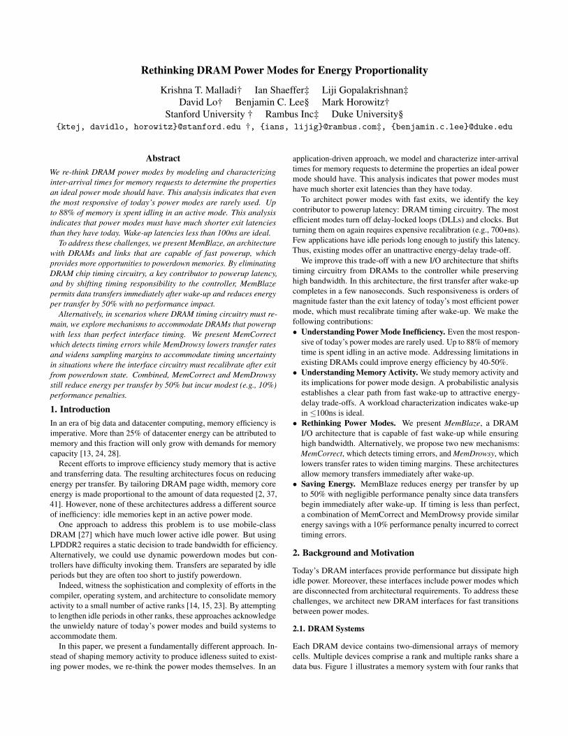
Each DRAM device contains two-dimensional arrays of memorycells. Multiple devices comprise a rank and multiple ranks share adata bus. Figure 1 illustrates a memory system with four ranks that
Figure 1: DDR3 DRAM Memory System. Figure 2: DDR3 DRAM Timing.
share a x64 channel. The number of channels and the interface’s datarate determine system bandwidth.
Each channel is attached to a memory controller, which is inte-grated on the processor die. To activate a row, the controller issuesa row access strobe (RAS) to enable word lines and buffers a row’sdata. To read and write, a column access strobe (CAS) transfersbuffered data to IO interfaces. Prefetching 8 bits across a 64b widechannel produces 64B to fill a processor cache line.2.2. DRAM InterfacesThe controller and DRAMs are connected by CA and DQ busesfor control and data signals. To synchronize signals, the controllergenerates and forwards a clock (CK) to the DRAMs. Controllercircuitry aligns this clock with command and enable signals. Becausethese signals have lower bandwidth and experience the same loadingconditions and discontinuities en route to DRAMs, skew is not anissue. Thus, commands and writes are synchronized.
However, synchronizing reads is more difficult. During a read,data signals are generated by DRAMs (DQ) while clock signalsare generated by the controller (CK). Originating on different dies,these signals are subject to different loading conditions and variationsin process, voltage, and temperature. Under these conditions, thecontroller has difficulty using CK edges to sample DQ for arrivingread data, especially at high frequencies and narrow data windows.
To facilitate read synchronization, DRAMs explicitly communicatedata timing to the controller with a data strobe signal (DQS) thatis aligned with the clock (CK) and bus data (DQ). The controllersamples DQ on DQS edges as illustrated in Figure 2. Data is availablesome latency after receiving a read command (RD on CA producesQ on DQ after tRL).
DQS edges and data windows must align with the controller-generated clock. DRAMs ensure alignment in two ways. First,during initialization, DQS and CK are calibrated to eliminate anyskew due to wire length while the controller specifies worst-casetolerance for timing differences (tDQSCK). Second, during opera-tion, delay-locked loops (DLLs) dynamically adjust the DRAM clockdelays to compensate for voltage and temperature variations and keepthe position of the DQS at the controller constant to reduce timinguncertainty when sampling data at high frequencies.2.3. DRAM Power Mode LimitationsConsider two scenarios in which DLLs affect efficiency. In the first,the DRAM is idling in an active power mode. In such an ’active-idle’
Power Mode DIMM Idle Exit Latency MechanismPower (W) (ns)
Active idle 5.36 0 nonePrecharge-idle 4.66 14 pages closedActive powerdown 3.28 6 clock, I/O buffers,
decode logic offFast exit powerdown 2.79 19.75 active powerdown
+ pages closedSlow exit powerdown 1.60 24 fast exit powerdown
+ DLL frozenSelf Refresh 0.92 768 fast exit powerdown
+ DLL, CK offSelf Refresh 0.56 6700 self refresh+ registers off + register PLLs offDisabled 0 disk latency DIMMs off
Table 1: Power Modes for a 4GB DDR3-x4-1333 RDIMM [5, 30]
state, the DLL and clocking power are a large fraction of the totalpower. For example, DDR3 active-idle current is 2× that of LPDDR2and much of this difference is attributed to the interface [27].
In a second scenario, which we call ’idle-idle’, the DRAM is ina powerdown mode. More efficient modes have higher poweruplatencies (e.g., self-refresh in Table 1). While this state seems energy-efficient, the next reference pays the cost as the DRAM spendstDLLK=512 active memory cycles (768ns) powering up the inter-face. This is a lot of energy. In addition, applications slow down, asindicated in Figure 3(a). Thus, existing DRAM interfaces imposeunattractive performance and power tradeoffs.
Static mechanisms to reduce interface power fare no better. Wecan configure the memory mode registers (MR) in the BIOS [30],eliminating DLLs but this imposes performance penalties. First,the peak data rate is halved as channel frequency must be loweredto ensure signal integrity. Furthermore, without DLLs, timing isless certain and controllers must assume worst-case margins (i.e.,tDQSCK=10ns [30]). Conservative timing increases critical wordlatency, affecting application performance as shown in (Figure 3(b)).
Due to these punishing trade-offs, memory controllers invokepower modes conservatively. Modern controllers recommend a pow-erdown threshold no lower than 15 idle memory cycles [17]. Figure4(a) shows the percent of time the DRAMs stay in each power statefor this aggressive threshold (A), a moderate (M) threshold 10×larger, and a conservative (C) threshold 100 × larger. With suchthresholds, up to 88% of memory time is in active-idle.
Potential for Efficiency. Suppose we were to address limitationsin today’s interfaces and power modes so that the most efficient
2
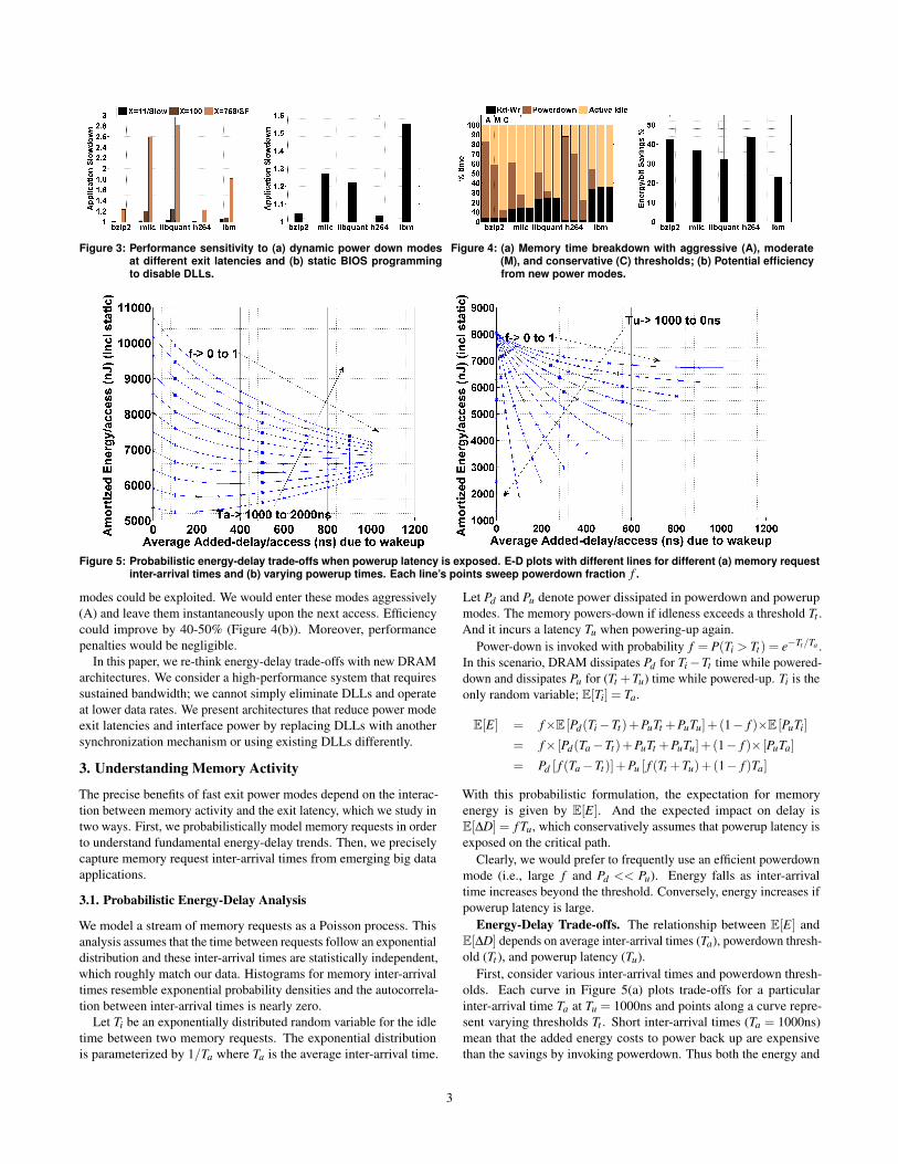
Figure 3: Performance sensitivity to (a) dynamic power down modesat different exit latencies and (b) static BIOS programmingto disable DLLs.
Figure 4: (a) Memory time breakdown with aggressive (A), moderate(M), and conservative (C) thresholds; (b) Potential efficiencyfrom new power modes.
Figure 5: Probabilistic energy-delay trade-offs when powerup latency is exposed. E-D plots with different lines for different (a) memory requestinter-arrival times and (b) varying powerup times. Each line’s points sweep powerdown fraction f .
modes could be exploited. We would enter these modes aggressively(A) and leave them instantaneously upon the next access. Efficiencycould improve by 40-50% (Figure 4(b)). Moreover, performancepenalties would be negligible.
In this paper, we re-think energy-delay trade-offs with new DRAMarchitectures. We consider a high-performance system that requiressustained bandwidth; we cannot simply eliminate DLLs and operateat lower data rates. We present architectures that reduce power modeexit latencies and interface power by replacing DLLs with anothersynchronization mechanism or using existing DLLs differently.
3. Understanding Memory Activity
The precise benefits of fast exit power modes depend on the interac-tion between memory activity and the exit latency, which we study intwo ways. First, we probabilistically model memory requests in orderto understand fundamental energy-delay trends. Then, we preciselycapture memory request inter-arrival times from emerging big dataapplications.
3.1. Probabilistic Energy-Delay Analysis
We model a stream of memory requests as a Poisson process. Thisanalysis assumes that the time between requests follow an exponentialdistribution and these inter-arrival times are statistically independent,which roughly match our data. Histograms for memory inter-arrivaltimes resemble exponential probability densities and the autocorrela-tion between inter-arrival times is nearly zero.
Let Ti be an exponentially distributed random variable for the idletime between two memory requests. The exponential distributionis parameterized by 1/Ta where Ta is the average inter-arrival time.
Let Pd and Pu denote power dissipated in powerdown and powerupmodes. The memory powers-down if idleness exceeds a threshold Tt .And it incurs a latency Tu when powering-up again.
Power-down is invoked with probability f = P(Ti > Tt) = e−Tt/Ta .In this scenario, DRAM dissipates Pd for Ti−Tt time while powered-down and dissipates Pu for (Tt +Tu) time while powered-up. Ti is theonly random variable; E[Ti] = Ta.
E[E] = f×E [Pd(Ti−Tt)+PuTt +PuTu]+ (1− f )×E [PuTi]
= f× [Pd(Ta−Tt)+PuTt +PuTu]+ (1− f )× [PuTa]
= Pd [ f (Ta−Tt)]+Pu [ f (Tt +Tu)+(1− f )Ta]
With this probabilistic formulation, the expectation for memoryenergy is given by E[E]. And the expected impact on delay isE[∆D] = f Tu, which conservatively assumes that powerup latency isexposed on the critical path.
Clearly, we would prefer to frequently use an efficient powerdownmode (i.e., large f and Pd << Pu). Energy falls as inter-arrivaltime increases beyond the threshold. Conversely, energy increases ifpowerup latency is large.
Energy-Delay Trade-offs. The relationship between E[E] andE[∆D] depends on average inter-arrival times (Ta), powerdown thresh-old (Tt ), and powerup latency (Tu).
First, consider various inter-arrival times and powerdown thresh-olds. Each curve in Figure 5(a) plots trade-offs for a particularinter-arrival time Ta at Tu = 1000ns and points along a curve repre-sent varying thresholds Tt . Short inter-arrival times (Ta = 1000ns)mean that the added energy costs to power back up are expensivethan the savings by invoking powerdown. Thus both the energy and
3
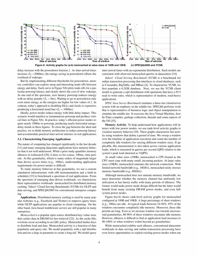
Figure 6: Activity graphs for (a-b) memcached at value sizes of 100B and 10KB. (c) SPECjbb2005 and YCSB.
delay increase with the powerdown fraction f . As inter-arrival timesincrease (Ta→2000ns), the energy saving in powerdown offsets theoverhead of wakeups.
But by implementing different thresholds for powerdown, mem-ory controllers can explore steep and interesting trade-offs betweenenergy and delay. Each curve in Figure 5(b) plots trade-offs for a par-ticular powerup latency and clearly shows the cost of slow wakeups.At one end of the spectrum, zero latency powerup reduces energywith no delay penalty (Tu = 0ns). Waiting to go to powerdown onlycosts more energy, as the energies are higher for low values of f . Incontrast, today’s approach to disabling DLLs and clocks is expensive,producing a horizontal trend line (Tu = 1000ns).
Ideally, power modes reduce energy with little delay impact. Thisscenario would manifest as instantaneous powerup and produce verti-cal lines in Figure 5(b). In practice, today’s efficient power modes re-quire nearly 1000ns to powerup, producing nearly horizontal energy-delay trends in these figures. To close the gap between the ideal andpractice, we re-think memory architecture to reduce powerup latencyand accommodate practical inter-arrival statistics in real applications.
3.2. Characterizing Emerging Applications
The nature of computing has changed significantly in the last decade[11] and many emerging datacenter applications have memory behav-ior that is not well understood. While a prior study quantifies memoryidleness in websearch [29], it does so for coarse, 100ms, time peri-ods. At this granularity, which is many orders of magnitude largerthan device access times (e.g., 100ns), understanding applicationrequirements for power modes is difficult.
To study memory behavior at fine granularity, we use a customsimulation infrastructure with x86 instrumentation and a built-inscheduler [33] to benchmark a spectrum of real applications. Fromthe spectrum of emerging data driven workloads, we characterizethree representative workloads: memcached for distributed memorycaching, Yahoo! Cloud Serving Benchmark (YCSB) for OLTP anddata serving, and SPECjbb2005 for conventional enterprise comput-ing.
Applications. Distributed memory caching is used by many pop-ular websites (e.g., Facebook and Twitter) to improve query timeswhile OLTP applications are popular in cloud computing. On theother hand, Java-based middleware servers are still popular in manyenterprises.
Memcached is a popular open source distributed key-value storethat caches data in DRAM for fast retrieval [32]. As the cache fills,evictions occur according to an LRU policy. Memcached hashes keysto distribute load and data. Memcached activity is a function of datapopularity and query rate. We model popularity with a zipf distribu-tion and use a large α parameter to create a long tail. We model query
inter-arrival times with an exponential distribution. Such models areconsistent with observed memcached queries in datacenters [34].
Yahoo! Cloud Serving Benchmark (YCSB) is a benchmark foronline transaction processing that interfaces to cloud databases, suchas Cassandra, BigTable, and HBase [4]. To characterize YCSB, wefirst populate a 6.2GB database. Next, we use the YCSB clientmodel to generate a zipf distribution with operations that have a 95:5read to write ratio, which is representative of modern, read-heavyapplications.
SPEC Java Server Benchmark emulates a three-tier client/serversystem with an emphasis on the middle tier. SPECjbb performs workthat is representative of business logic and object manipulation tosimulate the middle tier. It exercises the Java Virtual Machine, Just-In-Time compiler, garbage collection, threads and some aspects ofthe OS [35].
Memory Activity. To help understand how applications will in-teract with low power modes, we use rank-level activity graphs tovisualize memory behavior [29]. These graphs characterize bus activ-ity using windows that define a period of time. We sweep a windowover the timeline of application execution and count the number ofcompletely idle windows for varying different window sizes. If ap-plicable, this measurement is also taken across various applicationloads, which is measured in queries per second (QPS) relative to thesystem’s peak load (denoted as %QPS).
At small value sizes (100B), memcached is CPU-bound as theCPU must cope with many small, incoming packets. At large valuesizes (10KB), memcached saturates the network connection. Withlimited network bandwidth (e.g., 10Gb/s), memcached rarely stressesmemory bandwidth (e.g., 80Gb/s).
Although memcached does not saturate memory bandwidth, wemust determine whether the memory channel has uniformly lowutilization or has bursty traffic with many periods of idleness. Theformer would make power mode design difficult but the latter wouldbenefit from many existing DRAM power modes, and even full-system power modes.
Figure 6(a-b) shows rank-level activity graphs for memcachedconfigured at 100B and 10KB. A large percentage of short windows(e.g., 100ns) are idle. At typical loads between 10-50%, 95% of thewindows encounter completely idle memory. Moreover, these idleperiods are long. Even as we increase window size towards microsec-ond granularities, 80-90% of these windows encounter idle memory.However, idleness is difficult to find as application load increases to90-100% or when windows widen beyond µs granularities.
While memcached exhibits such idleness, conventional datacenterworkloads in data serving and online-transaction processing haveeven fewer opportunities to exploit existing power-modes when run
4
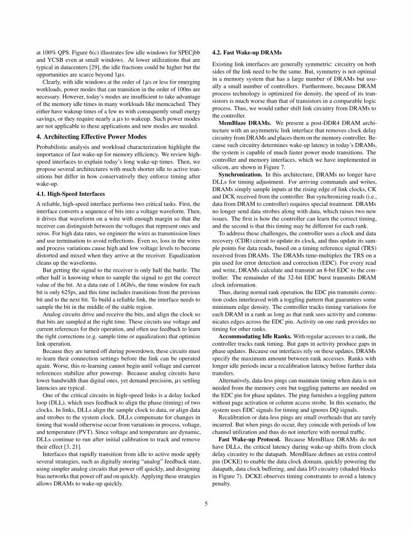
at 100% QPS. Figure 6(c) illustrates few idle windows for SPECjbband YCSB even at small windows. At lower utilizations that aretypical in datacenters [29], the idle fractions could be higher but theopportunities are scarce beyond 1µs.
Clearly, with idle windows at the order of 1µs or less for emergingworkloads, power modes that can transition in the order of 100ns arenecessary. However, today’s modes are insufficient to take advantageof the memory idle times in many workloads like memcached. Theyeither have wakeup times of a few ns with consequently small energysavings, or they require nearly a µs to wakeup. Such power modesare not applicable to these applications and new modes are needed.
4. Architecting Effective Power ModesProbabilistic analysis and workload characterization highlight theimportance of fast wake-up for memory efficiency. We review high-speed interfaces to explain today’s long wake-up times. Then, wepropose several architectures with much shorter idle to active tran-sitions but differ in how conservatively they enforce timing afterwake-up.
4.1. High-Speed Interfaces
A reliable, high-speed interface performs two critical tasks. First, theinterface converts a sequence of bits into a voltage waveform. Then,it drives that waveform on a wire with enough margin so that thereceiver can distinguish between the voltages that represent ones andzeros. For high data rates, we engineer the wires as transmission linesand use termination to avoid reflections. Even so, loss in the wiresand process variations cause high and low voltage levels to becomedistorted and mixed when they arrive at the receiver. Equalizationcleans up the waveforms.
But getting the signal to the receiver is only half the battle. Theother half is knowing when to sample the signal to get the correctvalue of the bit. At a data rate of 1.6Gb/s, the time window for eachbit is only 625ps, and this time includes transitions from the previousbit and to the next bit. To build a reliable link, the interface needs tosample the bit in the middle of the stable region.
Analog circuits drive and receive the bits, and align the clock sothat bits are sampled at the right time. These circuits use voltage andcurrent references for their operation, and often use feedback to learnthe right corrections (e.g. sample time or equalization) that optimizelink operation.
Because they are turned off during powerdown, these circuits mustre-learn their connection settings before the link can be operatedagain. Worse, this re-learning cannot begin until voltage and currentreferences stabilize after powerup. Because analog circuits havelower bandwidth than digital ones, yet demand precision, µs settlinglatencies are typical.
One of the critical circuits in high-speed links is a delay lockedloop (DLL), which uses feedback to align the phase (timing) of twoclocks. In links, DLLs align the sample clock to data, or align dataand strobes to the system clock. DLLs compensate for changes intiming that would otherwise occur from variations in process, voltage,and temperature (PVT). Since voltage and temperature are dynamic,DLLs continue to run after initial calibration to track and removetheir effect [3, 21].
Interfaces that rapidly transition from idle to active mode applyseveral strategies, such as digitally storing “analog” feedback state,using simpler analog circuits that power off quickly, and designingbias networks that power off and on quickly. Applying these strategiesallows DRAMs to wake-up quickly.
4.2. Fast Wake-up DRAMs
Existing link interfaces are generally symmetric: circuitry on bothsides of the link need to be the same. But, symmetry is not optimalin a memory system that has a large number of DRAMs but usu-ally a small number of controllers. Furthermore, because DRAMprocess technology is optimized for density, the speed of its tran-sistors is much worse than that of transistors in a comparable logicprocess. Thus, we would rather shift link circuitry from DRAMs tothe controller.
MemBlaze DRAMs. We present a post-DDR4 DRAM archi-tecture with an asymmetric link interface that removes clock delaycircuitry from DRAMs and places them on the memory controller. Be-cause such circuitry determines wake-up latency in today’s DRAMs,the system is capable of much faster power mode transitions. Thecontroller and memory interfaces, which we have implemented insilicon, are shown in Figure 7.
Synchronization. In this architecture, DRAMs no longer haveDLLs for timing adjustment. For arriving commands and writes,DRAMs simply sample inputs at the rising edge of link clocks, CKand DCK received from the controller. But synchronizing reads (i.e.,data from DRAM to controller) requires special treatment. DRAMsno longer send data strobes along with data, which raises two newissues. The first is how the controller can learn the correct timing,and the second is that this timing may be different for each rank.
To address these challenges, the controller uses a clock and datarecovery (CDR) circuit to update its clock, and thus update its sam-ple points for data reads, based on a timing reference signal (TRS)received from DRAMs. The DRAMs time-multiplex the TRS on apin used for error detection and correction (EDC). For every readand write, DRAMs calculate and transmit an 8-bit EDC to the con-troller. The remainder of the 32-bit EDC burst transmits DRAMclock information.
Thus, during normal rank operation, the EDC pin transmits correc-tion codes interleaved with a toggling pattern that guarantees someminimum edge density. The controller tracks timing variations foreach DRAM in a rank as long as that rank sees activity and commu-nicates edges across the EDC pin. Activity on one rank provides notiming for other ranks.
Accommodating Idle Ranks. With regular accesses to a rank, thecontroller tracks rank timing. But gaps in activity produce gaps inphase updates. Because our interfaces rely on these updates, DRAMsspecify the maximum amount between rank accesses. Ranks withlonger idle periods incur a recalibration latency before further datatransfers.
Alternatively, data-less pings can maintain timing when data is notneeded from the memory core but toggling patterns are needed onthe EDC pin for phase updates. The ping furnishes a toggling patternwithout page activation or column access strobe. In this scenario, thesystem uses EDC signals for timing and ignores DQ signals.
Recalibration or data-less pings are small overheads that are rarelyincurred. But when pings do occur, they coincide with periods of lowchannel utilization and thus do not interfere with normal traffic.
Fast Wake-up Protocol. Because MemBlaze DRAMs do nothave DLLs, the critical latency during wake-up shifts from clockdelay circuitry to the datapath. MemBlaze defines an extra controlpin (DCKE) to enable the data clock domain, quickly powering thedatapath, data clock buffering, and data I/O circuitry (shaded blocksin Figure 7). DCKE observes timing constraints to avoid a latencypenalty.
5
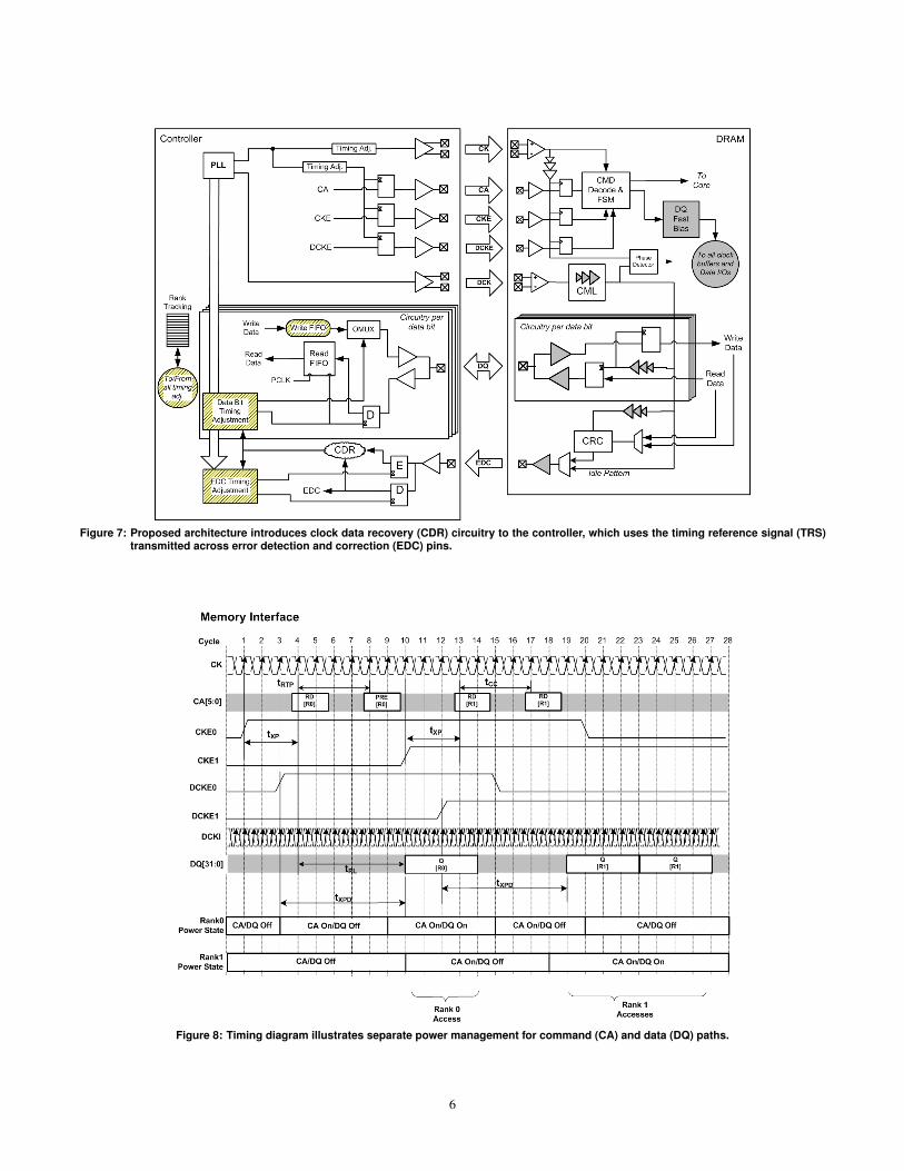
Figure 7: Proposed architecture introduces clock data recovery (CDR) circuitry to the controller, which uses the timing reference signal (TRS)transmitted across error detection and correction (EDC) pins.
Figure 8: Timing diagram illustrates separate power management for command (CA) and data (DQ) paths.
6
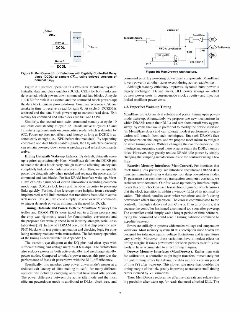
Figure 9: MemCorrect Error Detection with Digitally Controlled DelayLines (DCDL) to sample CKext using delayed versions ofnominal CKint .
Figure 8 illustrates operation in a two-rank MemBlaze system.Initially, data and clock enables (DCKE, CKE) for both ranks arede-asserted, which powers-down command and data blocks. At cycle1, CKE0 for rank 0 is asserted and the command block powers-up;the data block remains powered-down. Command receivers (CA) areawake in time to receive a read for rank 0. At cycle 3, DCKE0 isasserted and the data block powers-up to transmit read data. Exitlatency for command and data blocks are tXP and tXPD.
Similarly, the second rank exits command standby at cycle 10and exits data standby at cycle 12. Reads arrive at cycles 13 and17, satisfying constraints on consecutive reads, which is denoted bytCC. Power-up does not affect read latency as long as DCKE is as-serted early enough (i.e., tXPD before first read data). By separatingcommand and data block enable signals, the DQ interface circuitrycan remain powered-down even as precharge and refresh commandsarrive.
Hiding Datapath Wake-up Latency. By default, datapath wake-up requires approximately 10ns. MemBlaze defines the DCKE pinto enable the data block early enough to avoid affecting latency andcompletely hide it under column access (CAS). Thus, we can quicklypower the datapath only when needed and separate the powerups forcommand and data blocks. For fast DRAM interface wake-up, Mem-Blaze exploits a number of circuit innovations including common-mode logic (CML) clock trees and fast-bias circuitry to poweruplinks quickly. Further, if we leverage more insights from a recentlyimplemented serial link interface that transitions from idle to activewell under 10ns [40], we could simply use read or write commandsto trigger datapath powerup eliminating the need for DCKE.
Timing, Datarate and Power. Both the MemBlaze Memory Con-troller and DRAM PHYs were taped out in a 28nm process andthe chip was rigorously tested for functionality, correctness andthe proposed fast wakeup speed in an industry-strength, serial-linkslaboratory[19]. In lieu of a DRAM core, the test chip pairs the newPHY blocks with test pattern generation and checking logic for emu-lating memory read and write transactions. The laboratory operationof the timing is demonstrated in Appendix §A.
The transmit eye diagram at the DQ pins had clear eyes withsufficient timing and voltage margins at 6.4Gbps. The architecturealso reduces power in both active-standby and precharge-standbypower modes. Compared to today’s power modes, this provides theperformance of fast-exit powerdown with the DLL-off efficiency.
Specifically, this matches deep power down mode’s power at areduced exit latency of 10ns making it useful for many differentapplications including emerging ones that have short idle periods.The power difference between the active idle mode and the mostefficient powerdown mode is attributed to DLLs, clock tree, and
Figure 10: MemDrowsy Architecture.
command pins. By powering down these components, MemBlazelowers power in all other states except during active reads/writes.
Although standby efficiency improves, dynamic burst power islargely unchanged. During bursts, DLL power savings are offsetby new power costs in current-mode clock circuitry and injectionlocked-oscillator power costs.
4.3. Imperfect Wake-up Timing
MemBlaze provides an ideal solution and perfect timing upon power-mode wake-up. Alternatively, we propose two new mechanisms inwhich DRAMs retain their DLLs and turn them on/off very aggres-sively. Systems that would prefer not to modify the device interface(as MemBlaze does) and can tolerate modest performance degra-dation will benefit from such techniques. But such DRAMs facesynchronization challenges, and we propose mechanisms to mitigateor avoid timing errors. Without changing the controller-device linkinterface and operating speed these systems retain the DDRx memorylinks. However, they greatly reduce DRAM idle power by simplychanging the sampling rate/decision inside the controller using a fewflops.
Reactive Memory Interfaces (MemCorrect). For interfaces thattrack timing less precisely, we introduce speculative DRAM datatransfers immediately after waking up from deep powerdown modes.To guarantee that each memory transaction completes correctly, wearchitect error detectors. Our fast wake-up memory interface imple-ments this error check on each transaction (Figure 9), which ensuresthat the clock transition is within a window (±∆) of its nominal lo-cation. This check handles cases when variations and drift duringpowerdown affect link operation. The error is communicated to thecontroller through a dedicated pin, Correct. If an error occurs, it isbecause the controller has issued a command too soon after powerup.The controller could simply wait a longer period of time before re-trying the command or could send a timing calibrate command toexpedite wake-up.
Errors are unlikely in systems with modest voltage and temperaturevariations. Most memory systems fit this description since boards aredesigned for tolerance against voltage fluctuations and temperaturesvary slowly. Moreover, these variations have a modest effect ontiming margins if ranks powerdown for short periods as drift is lesslikely to have accumulated to affect timing margins.
Drowsy Memory Interfaces (MemDrowsy). Rather than waitfor calibration, a controller might begin transfers immediately butmitigate timing errors by halving the data rate for a certain periodof time (Y) after wake-up. This slower rate more than doubles thetiming margin of the link, greatly improving tolerance to small timingerrors induced by VT variations.
Thus, MemDrowsy reduces the effective data rate and relaxes tim-ing precision after wake-up, for reads that need a locked DLL. The
7
ACT
CK
CA[5:0]
DQ[31:0]
tRCD
DQ
CKE
tXP
RD
DQ
Normal
tCL
Drowsy
DQ
Read Write
Z * (BL/2) (BL/2) (BL/2)
Y
Deep
PD
Figure 11: MemDrowsy Timing Diagram.
clock speed is still maintained at the full rate but the link effectivelytransmits each bit twice. This enables transmitting data while recali-brating and results in lengthening the valid data window. Of course,the controller must also shift the point at which data is sampled. Afterrecalibration, the link operates at nominal data rates.
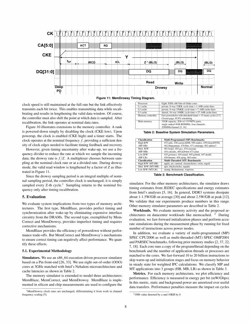
Figure 10 illustrates extensions to the memory controller. A rankis powered-down simply by disabling the clock (CKE low). Uponpowerup, the clock is enabled (CKE high) and a timer starts. Theclock operates at the nominal frequency f , providing a sufficient den-sity of clock edges needed to facilitate timing feedback and recovery.
However, given timing uncertainty after wake-up, we use a fre-quency divider to reduce the rate at which we sample the incomingdata; the drowsy rate is f/Z. A multiplexer chooses between sam-pling at the nominal clock rate or at a divided rate. During drowsymode, the valid read window is lengthened by a factor of Z as illus-trated in Figure 11.
Since the drowsy sampling period is an integral multiple of nomi-nal sampling period, the controller clock is unchanged; it is simplysampled every Z-th cycle.1 Sampling returns to the nominal fre-quency only after timing recalibration.
5. Evaluation
We evaluate system implications from two types of memory archi-tectures. The first type, MemBlaze, provides perfect timing andsynchronization after wake-up by eliminating expensive interfacecircuitry from the DRAMs. The second type, exemplified by Mem-Correct and MemDrowsy, provides imperfect timing and requirescorrective mechanisms.
MemBlaze provides the efficiency of powerdown without perfor-mance trade-offs. But MemCorrect and MemDrowsy’s mechanismsto ensure correct timing can negatively affect performance. We quan-tify these effects.
5.1. Experimental Methodology
Simulators. We use an x86_64 execution-driven processor simulatorbased on a Pin front-end [26, 33]. We use eight out-of-order (OOO)cores at 3GHz matched with Intel’s Nehalem microarchitecture andcache latencies as shown in Table 2.
The memory simulator is extended to model three architectures:MemBlaze, MemCorrect, and MemDrowsy. MemBlaze is imple-mented in silicon and chip measurements are used to configure the
1MemDrowsy clock rates are unchanged, differentiating it from work in channelfrequency scaling [5].
Processor Eight 3GHz x86 Out-of-Order coresL1 cache private, 8-way 32KB, cycle time = 1, 64B cache-linesL2 cache private, 8-way 256KB, cycle time = 7, 64B cache-linesL3 cache shared, 16-way 16MB, cycle time = 27, 64B cache-linesMemory controller Fast powerdown with threshold timer = 15 mem-cycles [17]
Closed-page, FCFS schedulingMain memory 32GB capacity, 2Gb x4 1333MT/s parts,
single ranked 4GB-RDIMMs, four channels,2DIMMs/channel [5, 16]
Table 2: Baseline System Simulation Parameters.
Classification Multi-Programmed (MP) BenchmarksHigh B/W 433.milc, 436.cactusADM, 450.soplex, 459.GemsFDTD,(MP-HB) 462.libquantum, 470.lbm, 471.omnetpp, 482.sphinx3Med. B/W 401.bzip2, 403.gcc, 434.zeusmp,(MP-MB) 454.calculix, 464.h264ref 473.astarLow B/W 435.gromacs, 444.namd, 445.gobmk, 447.dealll,(MP-LB) 456.hmmer, 458.sjeng, 465.tontoClassification Multi-Threaded (MT) BenchmarksHigh B/W (MT-HB) applu, art, canneal, streamcluster, swim, mgridMed. B/W (MT-MB) apsi, blackscholes, equakeLow B/W (MT-LB) ammp, fluidanimate, wupwise
Table 3: Benchmark Classification.
simulator. For the other memory architectures, the simulator drawstiming estimates from JEDEC specifications and energy estimatesfrom Intel’s analyses [5, 16]. In general, DDR3 systems dissipateabout 1-1.5W/GB on average [30] and about 2.5W/GB at peak [12].We validate that our experiments produce numbers in this range.Other memory simulator parameters are described in Table 2.
Workloads. We evaluate memory activity and the proposed ar-chitectures on datacenter workloads like memcached. 2 Duringevaluation, we fast-forward initialization phases and perform accu-rate simulations during the measurement phase by running for fixednumber of instructions across power modes.
In addition, we evaluate a variety of multi-programmed (MP)SPEC CPU2006 as well as multi-threaded (MT) SPEC OMP2001and PARSEC benchmarks, following prior memory studies [2, 37, 22,7, 18]. Each core runs a copy of the program/thread depending on thebenchmark and the number of application threads or processes arematched to the cores. We fast-forward 10 to 20 billion instructions toskip warm-up and initialization stages and focus on memory behaviorin steady state for weighted IPC calculations. We classify MP andMT applications into 3 groups (HB, MB, LB) as shown in Table 3.
Metrics. For each memory architecture, we plot efficiency andperformance. Efficiency is measured in energy per bit (mW/Gbps).In this metric, static and background power are amortized over usefuldata transfers. Performance penalties measure the impact on cycles
2100b value denoted by a and 10KB by b
8
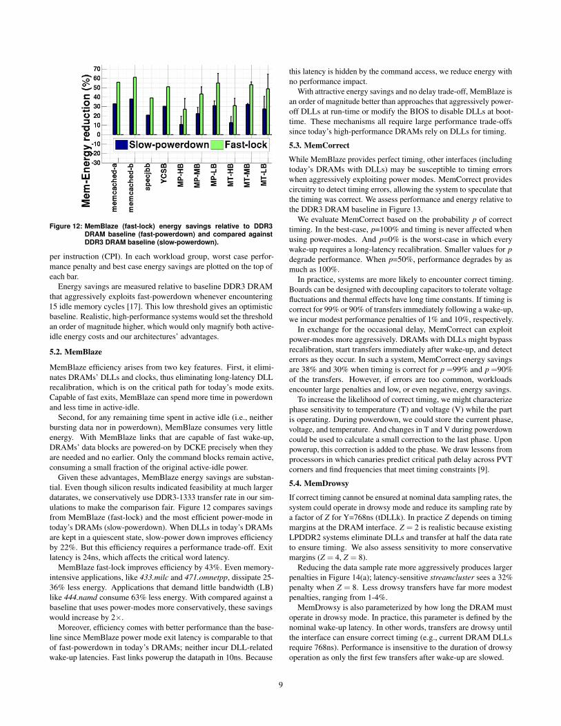
Figure 12: MemBlaze (fast-lock) energy savings relative to DDR3DRAM baseline (fast-powerdown) and compared againstDDR3 DRAM baseline (slow-powerdown).
per instruction (CPI). In each workload group, worst case perfor-mance penalty and best case energy savings are plotted on the top ofeach bar.
Energy savings are measured relative to baseline DDR3 DRAMthat aggressively exploits fast-powerdown whenever encountering15 idle memory cycles [17]. This low threshold gives an optimisticbaseline. Realistic, high-performance systems would set the thresholdan order of magnitude higher, which would only magnify both active-idle energy costs and our architectures’ advantages.
5.2. MemBlaze
MemBlaze efficiency arises from two key features. First, it elimi-nates DRAMs’ DLLs and clocks, thus eliminating long-latency DLLrecalibration, which is on the critical path for today’s mode exits.Capable of fast exits, MemBlaze can spend more time in powerdownand less time in active-idle.
Second, for any remaining time spent in active idle (i.e., neitherbursting data nor in powerdown), MemBlaze consumes very littleenergy. With MemBlaze links that are capable of fast wake-up,DRAMs’ data blocks are powered-on by DCKE precisely when theyare needed and no earlier. Only the command blocks remain active,consuming a small fraction of the original active-idle power.
Given these advantages, MemBlaze energy savings are substan-tial. Even though silicon results indicated feasibility at much largerdatarates, we conservatively use DDR3-1333 transfer rate in our sim-ulations to make the comparison fair. Figure 12 compares savingsfrom MemBlaze (fast-lock) and the most efficient power-mode intoday’s DRAMs (slow-powerdown). When DLLs in today’s DRAMsare kept in a quiescent state, slow-power down improves efficiencyby 22%. But this efficiency requires a performance trade-off. Exitlatency is 24ns, which affects the critical word latency.
MemBlaze fast-lock improves efficiency by 43%. Even memory-intensive applications, like 433.milc and 471.omnetpp, dissipate 25-36% less energy. Applications that demand little bandwidth (LB)like 444.namd consume 63% less energy. With compared against abaseline that uses power-modes more conservatively, these savingswould increase by 2×.
Moreover, efficiency comes with better performance than the base-line since MemBlaze power mode exit latency is comparable to thatof fast-powerdown in today’s DRAMs; neither incur DLL-relatedwake-up latencies. Fast links powerup the datapath in 10ns. Because
this latency is hidden by the command access, we reduce energy withno performance impact.
With attractive energy savings and no delay trade-off, MemBlaze isan order of magnitude better than approaches that aggressively power-off DLLs at run-time or modify the BIOS to disable DLLs at boot-time. These mechanisms all require large performance trade-offssince today’s high-performance DRAMs rely on DLLs for timing.
5.3. MemCorrect
While MemBlaze provides perfect timing, other interfaces (includingtoday’s DRAMs with DLLs) may be susceptible to timing errorswhen aggressively exploiting power modes. MemCorrect providescircuitry to detect timing errors, allowing the system to speculate thatthe timing was correct. We assess performance and energy relative tothe DDR3 DRAM baseline in Figure 13.
We evaluate MemCorrect based on the probability p of correcttiming. In the best-case, p=100% and timing is never affected whenusing power-modes. And p=0% is the worst-case in which everywake-up requires a long-latency recalibration. Smaller values for pdegrade performance. When p=50%, performance degrades by asmuch as 100%.
In practice, systems are more likely to encounter correct timing.Boards can be designed with decoupling capacitors to tolerate voltagefluctuations and thermal effects have long time constants. If timing iscorrect for 99% or 90% of transfers immediately following a wake-up,we incur modest performance penalties of 1% and 10%, respectively.
In exchange for the occasional delay, MemCorrect can exploitpower-modes more aggressively. DRAMs with DLLs might bypassrecalibration, start transfers immediately after wake-up, and detecterrors as they occur. In such a system, MemCorrect energy savingsare 38% and 30% when timing is correct for p =99% and p =90%of the transfers. However, if errors are too common, workloadsencounter large penalties and low, or even negative, energy savings.
To increase the likelihood of correct timing, we might characterizephase sensitivity to temperature (T) and voltage (V) while the partis operating. During powerdown, we could store the current phase,voltage, and temperature. And changes in T and V during powerdowncould be used to calculate a small correction to the last phase. Uponpowerup, this correction is added to the phase. We draw lessons fromprocessors in which canaries predict critical path delay across PVTcorners and find frequencies that meet timing constraints [9].
5.4. MemDrowsy
If correct timing cannot be ensured at nominal data sampling rates, thesystem could operate in drowsy mode and reduce its sampling rate bya factor of Z for Y=768ns (tDLLk). In practice Z depends on timingmargins at the DRAM interface. Z = 2 is realistic because existingLPDDR2 systems eliminate DLLs and transfer at half the data rateto ensure timing. We also assess sensitivity to more conservativemargins (Z = 4, Z = 8).
Reducing the data sample rate more aggressively produces largerpenalties in Figure 14(a); latency-sensitive streamcluster sees a 32%penalty when Z = 8. Less drowsy transfers have far more modestpenalties, ranging from 1-4%.
MemDrowsy is also parameterized by how long the DRAM mustoperate in drowsy mode. In practice, this parameter is defined by thenominal wake-up latency. In other words, transfers are drowsy untilthe interface can ensure correct timing (e.g., current DRAM DLLsrequire 768ns). Performance is insensitive to the duration of drowsyoperation as only the first few transfers after wake-up are slowed.
9
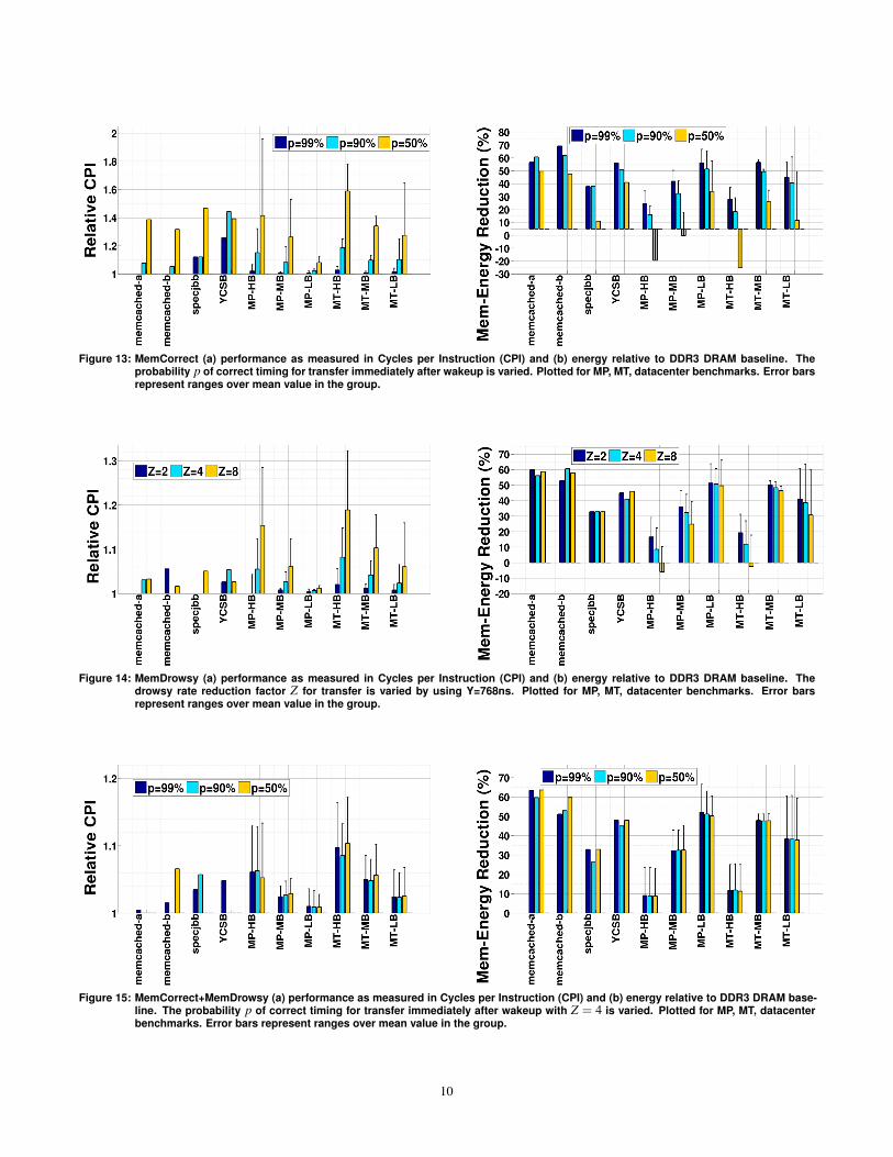
Figure 13: MemCorrect (a) performance as measured in Cycles per Instruction (CPI) and (b) energy relative to DDR3 DRAM baseline. Theprobability p of correct timing for transfer immediately after wakeup is varied. Plotted for MP, MT, datacenter benchmarks. Error barsrepresent ranges over mean value in the group.
Figure 14: MemDrowsy (a) performance as measured in Cycles per Instruction (CPI) and (b) energy relative to DDR3 DRAM baseline. Thedrowsy rate reduction factor Z for transfer is varied by using Y=768ns. Plotted for MP, MT, datacenter benchmarks. Error barsrepresent ranges over mean value in the group.
Figure 15: MemCorrect+MemDrowsy (a) performance as measured in Cycles per Instruction (CPI) and (b) energy relative to DDR3 DRAM base-line. The probability p of correct timing for transfer immediately after wakeup with Z = 4 is varied. Plotted for MP, MT, datacenterbenchmarks. Error bars represent ranges over mean value in the group.
10
For these modest penalties, MemDrowsy achieves significant en-ergy savings in Figure 14(b). Drowsy transfers allow applications toenter power modes more often with fewer penalties. Clearly, appli-cations that demand memory bandwidth (HB) are more sensitive todrowsy operation. Indeed, average energy per transfer might increasedue to larger termination energy from higher bus utilization and alsothe idle power during the extra cycles.
5.5. MemCorrect and MemDrowsy
Suppose MemCorrect detects a timing error for a transfer immediatelyfollowing a wake-up. Instead of delaying the transfer for the nominalwake-up latency, the system invokes MemDrowsy and begins thetransfer immediately at a slower rate. Clearly, performance andefficiency in MemCorrect+MemDrowsy will be better than eitherapproach applied individually. Immediately after wake-up, transfersbegin immediately either at the nominal or reduced data rate.
With MemCorrect+MemDrowsy, exploiting power modes andtransferring data immediately after wake-up has performance penal-ties between 10-20%, as shown in Figure 15(a). In exchange, powermodes are more often exploited and energy savings are more consis-tent.
When implemented alone, MemCorrect energy savings are verysensitive to the probability of correct timing after wake-up. In combi-nation, however, MemCorrect+MemDrowsy is insensitive to timingrisk, as shown in Figure 15(b). As MemDrowsy improves mem-ory channel utilization, background power is amortized over moretransfers.
MemBlaze promises large energy savings with an architecture thatprovides perfect timing information. Without such timing guarantees,however, MemCorrect+MemDrowsy provide the next best thing:comparable efficiency and modest (<10%) performance degradationfor many applications.
6. Related Work
Much prior work reduces power in conventional server memory.Memory systems can statically set voltage and frequency at boottime, typically in the BIOS [7]. Frequency scaling reduces powerbut since the static power is amortized over few accesses at lowutilizations, the energy per memory access is still expensive. Theenergy per access could also increase due to higher bus utilizationfrom scaling [5].
Malladi et al. studied LPDDR2 in servers to trade bandwidthfor reduced active-idle power [27]. In the current paper, we con-vert DDR3 active-idle time to time in efficient powerdown withoutaffecting bandwidth. Lim et al. consider various grades of DDRmemory [25, 24] while Kgil et al. consider memory-processor stack-ing [20]. In contrast, we propose changes to power-hungry DRAMinterfaces.
Prior work also manages DRAM data placement, increasing ac-cess locality and creating opportunities to transition between powerstates [10, 23, 36, 8, 31, 1]. Prior work studies compiler strategiesfor cluster accesses by inserting NOPs or reordering to coalesce re-quests [6]. Also, pages might be redirected to particular DRAM ranksto create hot and cold memory spaces [14]. Memory controllers canthrottle requests to manage power [15]. In contrast, our work im-proves powermode efficiency as multiple studies highlight increasingdifficulty of finding usable idle times [7, 29].
We build upon detailed studies of Meisner et al. about subsys-tem characterization [29], and Ferdman et al. insights on scale out
workloads [11]. We study memory bus activity at finer granularities,enabling the analysis and design of DRAM power modes.
Given wide accesses internal to DRAM, chips have been proposedto reduce the number of parts activated. One approach reduces accessgranularity through separately controlled parts (e.g.,chips, ranks,banks, etc.) to create smaller, independent memory spaces [2, 37, 39,41]. However, reducing the size of the DRAM activated increases thenumber of peripheral circuits and degrades density [38].
7. Conclusion
In server memory, idle power can comprise 60-70% of the total. Mem-ory ranks spend 45-60% of their time idle. The spectrum of memoryarchitectures presented in this paper demonstrate new interfaces andarchitectures that address this problem. By eliminating or mitigat-ing long-latency DLL wake-ups, these systems aggressively usesefficient powerdown states during short idle periods with negligibleperformance penalty.
Benefits are particularly pronounced for high-capacity, multi-ranksystems with frequent idleness. We demonstrate energy savings of upto 68% in a four-rank memory system. While MemBlaze reduces idlepower with no performance impact on the system, MemDrowsy andMemCorrect accomplish similar power savings with low penalties.A MemBlaze test chip has also been fabricated and demonstrated tofunction at a high datarate of 6.4Gbps while the exit latencies and idlepower are verified with hardware measurements. Overall, we demon-strate possible techniques to build scalable, energy-proportional mem-ory systems for the future.
8. Acknowledgments
We sincerely thank Yi Lu for helping us with lab measurements,James Tringali, Hongzhong Zheng, Jared Zerbe for their useful dis-cussion. This project is supported in part by a Google Focused Re-search Award. Krishna Malladi is supported by Benchmark-CapitalStanford Graduate Fellowship. Benjamin Lee is supported in part byNSF grant CCF-1149252.
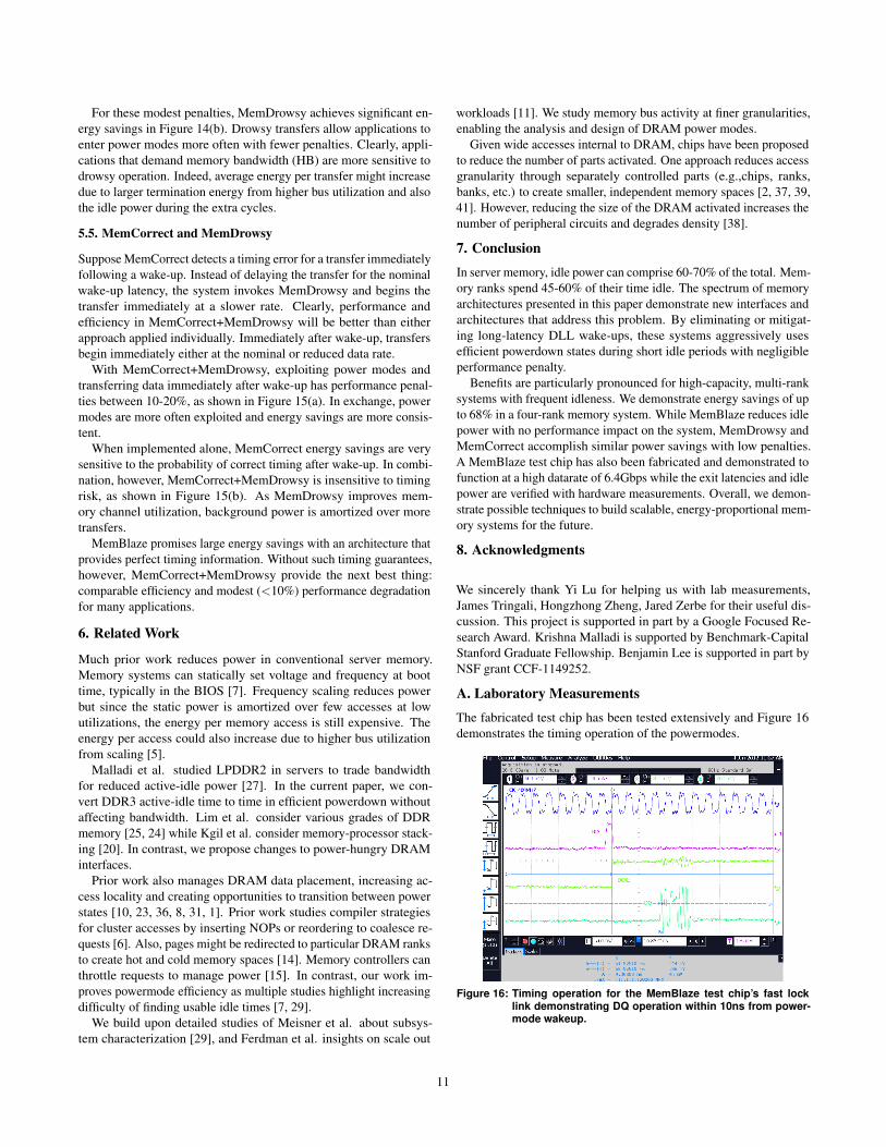
A. Laboratory Measurements
The fabricated test chip has been tested extensively and Figure 16demonstrates the timing operation of the powermodes.
Figure 16: Timing operation for the MemBlaze test chip’s fast locklink demonstrating DQ operation within 10ns from power-mode wakeup.
11
References[1] N. Aggarwal et al. Power-energycient DRAM speculation. In High
Performance Computer Architecture, 2008.[2] J. H. Ahn, N. P. Jouppi, C. Kozyrakis, J. Leverich, and R. S. Schreiber.
Future scaling of processor-memory interfaces. In SC, 2009.[3] Chih-Kong and K. Yang. Delay-locked loops - an overview. In Phase
Locking in High-Performance Systems. IEEE Press, 2003.[4] B. F. Cooper, A. Silberstein, E. Tam, R. Ramakrishnan, and R. Sears.
Benchmarking cloud serving systems with YCSB. In ACM Symposiumon Cloud Computing, 2010.
[5] H. David, O. Mutlu, et al. Memory power management via dynamicvoltage/frequency scaling. In ICAC, 2011.
[6] V. Delaluz, M. Kandemir, N. Vijaykrishnan, A. Sivasubramaniam, andM. Irwin. DRAM energy management using software & hardwaredirected power mode control. In High Performance Computer Architec-ture, 2001.
[7] Q. Deng, D. Meisner, L. Ramos, T. F. Wenisch, and R. Bianchini.Memscale: Active low-power modes for main memory. In InternationalConference on Architectural Support for Programming Languages andOperating Systems, 2011.
[8] B. Diniz, D. Guedes, and R. Bianchini. Limiting the power consumptionof main memory. In International Symposium on Computer Architecture,2007.
[9] D. Ernst, N. S. Kim, S. Das, S. Lee, D. Blaauw, T. Austin, T. Mudge,and K. Flautner. Razor: A low-power pipeline based on circuit-leveltiming speculation. In International Symposium on Microarchitecture,2003.
[10] X. Fan, C. Ellis, and A. Lebeck. Memory controller policies for DRAMpower management. In International Symposium on Low Power Elec-tronics and Design, 2001.
[11] M. Ferdman, A. Adileh, O. Kocberber, S. Volos, M. Alisafaee, D. Jevd-jic, C. Kaynak, A. D. Popescu, A. Ailamaki, and B. Falsafi. Clearing theclouds: a study of emerging scale-out workloads on modern hardware.In International Conference on Architectural Support for ProgrammingLanguages and Operating Systems, 2012.
[12] Hewlett-Packard. DDR3 memory technology. Technology briefTC100202TB, Hewlett-Packard, 2010.
[13] U. Hoelzle and L. Barroso. The Datacenter as a Computer. Morganand Claypool, 2009.
[14] H. Huang, K. G. Shin, C. Lefurgy, and T. Keller. Improving energyefficiency by making DRAM less randomly accessed. In InternationalSymposium on Low Power Electronics and Design, 2005.
[15] I. Hur and C. Lin. A comprehensive approach to DRAM power man-agement. In High Performance Computer Architecture, 2008.
[16] Intel. Intel memory 3-sigma power analysis methodology. Data sheet,Intel.
[17] Intel. Intel xeon processor e3-1200 family datasheet. Data sheet, Intel,2011.
[18] A. Jaleel, K. B. Theobald, S. C. S. Jr, and J. Emer. High performancecache replacement using re-reference interval prediction (RRRIP). InInternational Symposium on Computer Architecture, 2010.
[19] K. Kaviani et al. A 6.4-Gb/s near-ground single-ended transceiver fordual-rank dimm memory interface systems. In International Solid-StateCircuits Conference, February 2013.
[20] T. Kgil et al. PicoServer: Using 3D stacking technology to enable a com-pact energy efficient chip multiprocessor. In International Conferenceon Architectural Support for Programming Languages and OperatingSystems, 2006.
[21] J. Kim, M. Horowitz, and G.-Y. Wei. Design of cmos adaptive-bandwidth plls/dlls: A general approach. In IEEE Transactions onCircuits and Systems-II: Analog and Digital Signal Processing, 2003.
[22] Y. Kim, M. Papamichael, O. Mutlu, and M. Harchol-Balter. Threadcluster memory scheduling: Exploiting differences in memory accessbehavior. In International Symposium on Microarchitecture, 2010.
[23] A. Lebeck, X. Fan, H. Zeng, , and C. Ellis. Power aware page allocation.In International Conference on Architectural Support for ProgrammingLanguages and Operating Systems, 2000.
[24] K. Lim, J. Chang, T. Mudge, P. Ranganathan, S. K. Reinhardt, and T. F.Wenisch. Disaggregated memory for expansion and sharing in bladeservers. In International Symposium on Computer Architecture, 2009.
[25] K. Lim, P. Ranganathan, J. Chang, C. Patel, T. Mudge, and S. Reinhardt.Understanding and designing new server architectures for emerging
warehouse-computing environments. In International Symposium onComputer Architecture, 2008.
[26] C. Luk et al. Pin: Building customized program analysis tools withdynamic instrumentation. In PLDI, 2005.
[27] K. Malladi, F. Nothaft, K. Periyathambi, B. Lee, C. Kozyrakis, andM. Horowitz. Towards energy-proportional datacenter memory withmobile DRAM. In International Symposium on Computer Architecture,2012.
[28] D. Meisner, B. Gold, and T. Wensich. PowerNap: Eliminating serveridle power. In International Symposium on Computer Architecture,2009.
[29] D. Meisner, C. M. Sadler, L. A. Barroso, W.-D. Weber, and T. F. Wenisch.Power management of online data-intensive services. In InternationalSymposium on Computer Architecture, 2011.
[30] Micron. Micron 2Gb: x4, x8, x16 DDR3 SDRAM. Data SheetMT41J128M16HA-125, Micron, 2010.
[31] V. Pandey, W. Jiang, Y. Zhou, and R. Bianchini. DMA-aware memoryenergy management. In High Performance Computer Architecture,2006.
[32] P. Saab. Scaling memcached at Facebook. Facebook Engineering Note,2008.
[33] D. Sanchez et al. The ZCache: Decoupling ways and associativity. InInternational Symposium on Microarchitecture, 2011.
[34] N. Sharma, S. Barker, D. Irwin, and P. Shenoy. Blink: Managing serverclusters on intermittent power. In International Conference on Archi-tectural Support for Programming Languages and Operating Systems,2011.
[35] K. Shiv et al. SPECjvm2008 performance characterization. In SPECBenchmark Workshop on Computer Performance Evaluation and Bench-marking, 2009.
[36] M. Tolentino et al. Memory MISER: Improving main memory energyefficiency in servers. IEEE Trans, 2009.
[37] A. N. Udipi, N. Muralimanohar, N. Chatterjee, R. Balasubramonian,A. Davis, and N. P. Jouppi. Rethinking DRAM design and organizationfor energy-constrained multi-cores. In International Symposium onComputer Architecture, 2010.
[38] T. Vogelsang. Understanding the energy consumption of dynamic ran-dom access memories. In International Symposium on Microarchitec-ture, 2010.
[39] F. Ware and C. Hampel. Improving power and data efficiency withthreaded memory modules. In International Conference on ComputerDesign, 2006.
[40] J. Zerbe, B. Daly, L. Luo, B. Stonecypher, W. D. Dettloff, J. C. Eble,T. Stone, J. Ren, B. S. Leibowitz, M. Bucher, P. Satarzadeh, Q. Lin,Y. Lu, and R. Kollipara. A 5gb/s link with matched source synchronousand common-mode clocking techniques. In IEEE Journal of Solid-StateCircuits, 2011.
[41] H. Zheng, J. Lin, Z. Zhang, E. Gorbatov, H. David, and Z. Zhu. Mini-rank: Adaptive DRAM architecture for improving memory power effi-ciency. In International Symposium on Microarchitecture, 2008.
12