Embed Size (px)
Citation preview
Progress In Electromagnetics Research B, Vol. 30, 337–353, 2011
RESONANCE WAVELENGTH DEPENDENCE AND MODEFORMATION IN GOLD NANOROD OPTICAL ANTEN-NAS WITH FINITE THICKNESS
T. Dattoma, M. Grande*, R. Marani, G. Morea, V. Marrocco,and A. D’Orazio
Dipartimento di Elettrotecnica ed Elettronica, Politecnico di Bari, ViaRe David 200, Bari 70125, Italy
Abstract—In this paper we analyze the dependence of the resonancewavelength and mode formation of an optical gold nanorod antenna onits geometrical parameters in the wavelength range 500–1400 nm. Inparticular, we prove that nanoantennas differ from RF counterparts,since the minima and maxima, i.e., nodes and anti-nodes, of theresonant modes do not go to zero and show very intense peak at thecorners due to non-negligible thickness. Moreover, FDTD simulationsreveal that the usually considered linear relation between the resonantwavelength and the nanorod length has to be modified when thenanorod thickness is taken into account.
1. INTRODUCTION
Optical nanoantennas are metal nanostructure-based devices ableto convert the energy coming from free propagating radiation intolocalized energy and vice versa [1–3]. These nanoscaled metallicstructures possess a wide variety of extraordinary optical propertieswhich assume essential roles in applications such as efficient lightlocalization [4, 5], high resolution microscopy and spectroscopy [6–8], sensing [9, 10], photodetection [11, 12], light emission [13–15] andphotovoltaics [16–18]. For many years technological difficulty inaccessing nanoscale accuracy has strongly slowed down nanoantennasdevelopment, but in the last decade the impressive improvementsin nanotechnology have removed this main limit and opened up thepossibility to build antennas operating in the visible and infraredspectral ranges [19, 20].
Received 21 April 2011, Accepted 17 May 2011, Scheduled 22 May 2011* Corresponding author: Marco Grande ([email protected]).
338 Dattoma et al.
The optical characteristics of differently shaped optical antennas(monopole antennas, dipole antennas, Yagi-Uda antennas, particleantennas, slot antennas, patch antennas, gap antennas) and thedependence of the antenna field enhancement and spectral response onthe geometrical parameters have been already deeply discussed [21–35], also comparing both numerical [33] and experimental [32] results.Moreover, the scattering and absorption properties attributable tosingle noble metal nanoparticle having different shape (spherical,hemispherical, rectangular prism, triangular prism, cross-shape,etc. . . ) and patterned nanoparticle arrays with different period havealso been thoroughly investigated [36–39].
The design of an optical nanoantenna requires great attentionsince the conventional radiofrequency and microwave design rules thatdescribe antenna parameters as a function of the operating wavelengthare no longer valid [1–3]. In the high frequency regime, where thenanoantenna works, the metals show a strongly dispersive behaviourand their physical properties approach those of dielectrics. Therefore,since metals at optical frequencies behave in a different fashion withrespect to perfect conductors, the electromagnetic field is not perfectlyreflected by the metal surface and, on the contrary, penetrates insidethe metal at a well-determined depth (skin depth). This relevantpenetration depth is the consequence of the increased inertia, exhibitedby the conductor electrons as an external optical radiation is applied,which determines a delay in their response. Moreover, as immediateeffect of this phenomenon, at optical frequencies the incident radiationcouples to the electron plasma, which models the metal electrons,causing the formation of rapid oscillations. The implicit consequence ofthis event is that electrons in metals do not respond to the wavelengthof the incident radiation λ but to an effective wavelength λeff thatcan be expressed by a simple linear scaling rule as a function ofthe incident beam wavelength and of the plasma wavelength λp [40].Other important challenges, not deeply explored yet, in the designof optical nanoantennas are: the impedance matching between theantenna and the source, the electro-optical transduction, the phasecontrol of coupled optical antennas, antenna feeding, the dependenceof the transmitting and receiving antenna on the radiation pattern,on the angular response pattern, on the type of antenna and on thecharacteristics of the surrounding medium and so on [41–46].
In this paper we will discuss, for the first time to the bestof our knowledge, the dependence of resonant wavelengths of anoptical nanoantenna, which is a gold nanorod located on a GalliumNitride (GaN) substrate, on its geometrical parameters. We willshow how resonant modes are generated and distributed on the metal-
Progress In Electromagnetics Research B, Vol. 30, 2011 339
dielectric interfaces. The electric field distributions, evaluated in thenanoantenna region through the spatial Discrete Fourier Transform(DFT), will be compared with those of the RF antenna counterparts.Finally, we will show how the geometrical parameters such as lengthand thickness affect the nanoantenna resonant wavelength.
2. DEFINITION OF THE NANOANTENNA GEOMETRYAND NUMERICAL METHOD
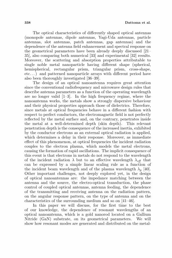
Figure 1 shows the sketch of the structure under investigation. Itconsists of a gold nanorod placed on a substrate of gallium nitride. Thechoice of gallium nitride as substrate is due to its optical properties,since this dielectric can be successfully employed as active material orin nonlinear nanoantennas-based applications.
Figure 1. Sketch of the analyzed structure and definition of thecomputational domain.
The numerical analysis has been performed by using an open-source Finite Difference Time Domain (FDTD) code [47]. Theimplementation of metallic objects requires the definition of amodel able to fit the experimental data of gold complex dielectricpermittivity [48]. The following relation describes the Drude-Lorentzmodel [49] used to model Au physical properties:
εm(ω) = ε∞ − ω2D
ω2 + jωγD−
2∑
k=1
δkω2k
ω2 − ω2k + 2jωγk
(1)
where ε∞ is the metal dielectric constant at the high frequency regimein the Drude model, ωD and γD are the plasma and collision frequenciesof the free electron gas related to the Drude model, whereas δi, ωi and
340 Dattoma et al.
γi, i = 1, 2, define amplitude, resonant angular frequency and dampingconstant of each Lorentz-like oscillator, respectively. The values of eachparameter of the dielectric function model, fitting the experimentaldata of gold reported in [50] are: ε∞ = 5.398, ωD = 1.398 · 1016 rad/s,γD = 1.033 · 1014 rad/s, δ1 = 0.681, ω1 = 4.274 · 1016 rad/s, γ1 =4.353 · 1014 rad/s, δ2 = 1.861, ω2 = 5.225 · 1016 rad/s and γ2 =6608 · 1014 rad/s [51].
Moreover, the considered geometrical parameters of the goldnanorod, length L and thickness d, range from 150 nm up to 850 nm andfrom 20 nm up to 200 nm, respectively. Without loss of generality andfocusing on the main goal of the current study, the refractive index ofthe gallium nitride substrate [52], the ordinary one (no), has been fixedto the constant value of 2.36. Anyway to test the effectiveness of ourresults, we have verified that, in the wavelength range of interest (500–1400 nm), when the dispersion of the material is taken into account,the following considerations are still valid.
The incident field for FDTD computation is a p-polarized planewave having a Gaussian temporal behaviour, tuned between 500 nmand 1400 nm. The electric field (E), whose unique component is alongthe y-direction, and the polarization (P ) are defined parallel to thenanorod whilst the magnetic field comes out from figure plane (z-direction).
In all calculations, the excitation surface and the reflection planeare placed 100 and 60 nm, respectively, far from the top boundary.The spatial resolution is set equal to 2 nm in both the directions ofthe computational domain and 20 Perfectly Matched Layers (PMLs)are used to truncate the simulation area. The PML thickness is keptconstant for each simulation and the distance between the nanorodand the domain boundaries is set equal to 200 nm on both sides in they-direction.
3. ANALYSIS OF THE RESONANT MODE FORMATION
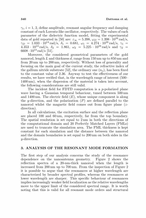
The first step of our analysis concerns the study of the resonancedependence on the nanoantenna geometry. Figure 2 shows thereflection spectra of a 20-nm-thick nanorod when the length isincreased from 200 nm up to 700 nm. From the inspection of Figure 2it is possible to argue that the resonances at higher wavelength arecharacterized by broader spectral profiles, whereas the resonances atlower wavelength are sharper. This specific behaviour of resonancesimplies increasingly weaker field localization as the relative wavelengthsmove to the upper limit of the considered spectral range. It is worthnoting that this is valid for all resonant mode orders and structural
Progress In Electromagnetics Research B, Vol. 30, 2011 341
(a) (b)
(c) (d)
Figure 2. Reflection spectra of 20-nm-thick nanorods havinglength equal to (a) 200 nm, (b) 400 nm, (c) 600 nm and (d) 700 nm,respectively.
configurations [53, 54].In addition, fixed the nanorod thickness, the resonant modes tend
to move from lower to higher wavelengths as the nanorod length isincreased changing their mode order. In Figure 2(a) (length L =200 nm) the first order and the second order resonant modes are placedat wavelengths equal to λ = 1068 nm and λ = 631 nm, respectively. Asthe length increases (Figure 2(b) L = 400 nm, Figure 2(c) L = 600 nm,Figure 2(d) L = 700 nm), the first order mode pulls out of the spectralrange of interest and the third order and the fourth order modes pull in.For instance, fixing the length L = 400 nm, the mode at the wavelengthλ = 885 nm is a second order mode, while the mode at the wavelengthλ = 659 nm is a third order mode.
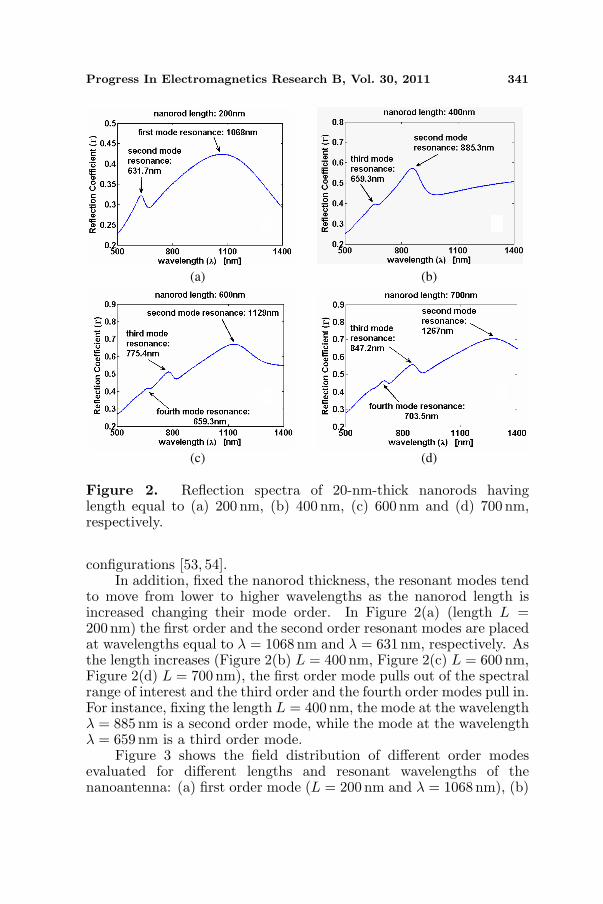
Figure 3 shows the field distribution of different order modesevaluated for different lengths and resonant wavelengths of thenanoantenna: (a) first order mode (L = 200 nm and λ = 1068 nm), (b)
342 Dattoma et al.
(a) (b)
(c) (d)
Figure 3. Details of the spatial Discrete Fourier Transforms of |Etot|2calculated at the resonant wavelength for the (a) first (L = 200 nmand λ = 1068 nm), (b) second (L = 400 nm and λ = 885 nm), (c)third (L = 600 nm and λ = 659 nm) and (d) fourth (L = 700 nm andλ = 703 nm) order modes reported in Figure 2 (d equal to 20 nm). Thelength of each nanoantenna has been chosen properly in order to showthe first four orders of resonance.
second order mode (L = 400 nm and λ = 885 nm), (c) third order mode(L = 600 nm and λ = 659 nm) and (d) fourth order mode (L = 700 nmand λ = 703 nm). This figure puts in evidence the effect of electricfield localization at the metal-dielectric and metal-air interfaces. Thefield confinement at these interfaces is due to the greater value of thepropagation constant with respect to the wave number in the dielectric,which determines the evanescently decay of field on both sides of eachinterface [55] and prevents it from propagating away from the interface.Therefore, along the interfaces Localized Surface Plasmon (LSP) canbe individualized within the direction perpendicular to the nanorodsurface, which is the oscillating direction of the conduction electrons.Moreover, at both interfaces the difference in the penetration depth [56]
Progress In Electromagnetics Research B, Vol. 30, 2011 343
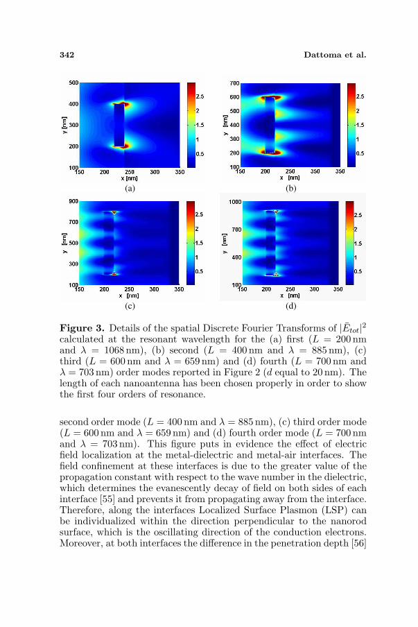
Figure 4. Reflection spectrum of 60-nm-thick nanorod having lengthL equal to 400 nm.
in the metal and dielectric layer can be emphasized, revealing amore consistent presence of field at the gold-GaN interface, since therefractive index of GaN is greater than that of the air.
Figure 4, which depicts the reflection spectrum when the antennalength and thickness are equal to 400 nm and 60 nm, respectively,allows to discuss also the dependence of the resonant wavelengths onthe nanorod thickness. In particular, the comparison between thespectra reported in Figure 4 and Figure 2(b) highlights how, for afixed length, resonant modes show tremendous difference in spectralpositions as the nanorod thickness is varied. For instance the secondmode resonance is placed at λ = 885 nm and λ = 792 nm for d equal to20 nm and 60 nm, respectively. Therefore in the nanoantenna design wecannot prevent from taking into account the thickness as fundamentalparameter.
In the optical plasmonic structure, for each resonant wavelengtha LSP mode is excited with a field profile strongly affected by thechoice of materials and elements shape [57]. Since the LSP resonanceof the metal nanorod is able to direct light from the source emitter ina way resembling the radiowave and microwave antennas [25], whosefield profiles along the metallic components are completely known, acomparison between the field of the analyzed nanoantenna and thefield profiles of a RF dipole antenna becomes a straightforward topic.Hereinafter, we will consider only the Au/GaN interface because theresonances at the opposite face fall at lower wavelengths, where thegold absorption is not negligible and thus air-LSPRs do not interactwith those emerging on the nanorod side which lies on GaN substrate.
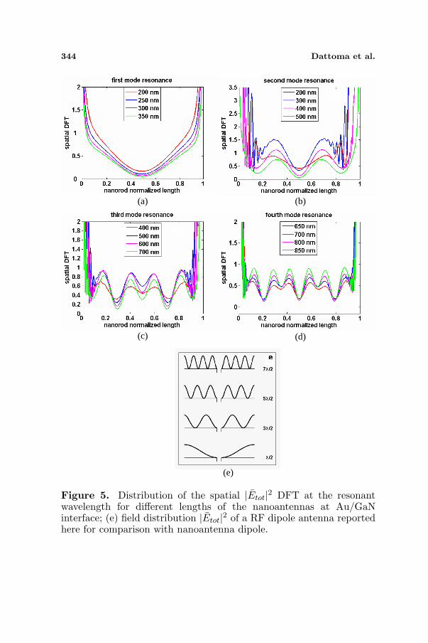
Figure 5 shows the electric field profiles of each mode order,evaluated for nanoantennas having different lengths, as shown in the
344 Dattoma et al.
(a) (b)
(c) (d)
(e)
Figure 5. Distribution of the spatial |Etot|2 DFT at the resonantwavelength for different lengths of the nanoantennas at Au/GaNinterface; (e) field distribution |Etot|2 of a RF dipole antenna reportedhere for comparison with nanoantenna dipole.
Progress In Electromagnetics Research B, Vol. 30, 2011 345
inset of the figure. To better visualize the graphs, the y-axis has beennormalized to the longest one. As in the RF case, a full correspondenceof the nodes and anti-nodes positions can be noted for all the consideredlengths of the nanoantenna, but the profile minimum values do notreach the zero in the nanoantennas, due to the penetration of the fieldin the metal layer (skin effect). Furthermore, as the length increases,the difference among minima and maxima is accentuated showing themode formation process and the diversity of the electric field profilesfor each resonant mode.
Another important difference is related to the presence of high-localized spot at the nanoantenna corners due to the presence of theangled tips. Angled tips, together with the finite thickness, which iscomparable to the nanoantennas length, induce the presence of highlyintense spots, whose level is considerably huger than maxima peaks, asclearly observable in Figure 5. As a confirmation, when the thicknessof the nanoantenna is reduced to the resolution step (2 nm) the peaksare still evident at the corners. In this way the mathematical solutionof Maxwell’s equations holds its validity, without being in contrast tothe physical principle of scattering by corners. Instead, in the RF case,being the thickness negligible with respect to the electrical length, atthe ends of the antenna, the entity of field is comparable with that inthe maxima (Figure 5(e)).
In the RF dipole antenna, the resonance condition occurs when itslength is equivalent to n · λ/2 (n being an integer) and the resonanceorder can be easily individuated by observing the number of periodsof the field wave along the metallic element. By analogy with the RFcase, in the analyzed nanoantenna the resonance condition follows theequation [58]:
L =(
m +12
)λeff (with m = n− 1) (2)
so that the first four resonance orders (n = 1, 2, 3, 4) correspondto nanoantenna lengths equal to λeff /2, 3λeff /2, 5λeff /2, 7λeff /2,respectively. Thus, for the first order the minimum of the distributioncan be interpreted as the dipole-like configuration, while for the otherthree resonance orders two, four and six peaks are observable in thecorresponding distribution respectively, as the graphs in Figure 5reveal.
4. RESONANT WAVELENGTH RELATION
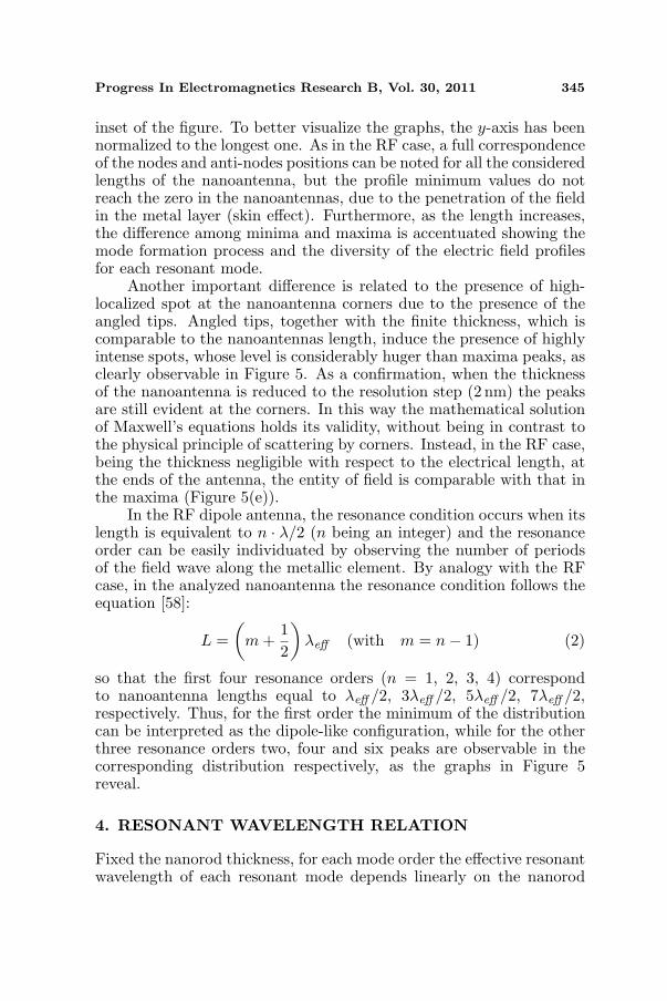
Fixed the nanorod thickness, for each mode order the effective resonantwavelength of each resonant mode depends linearly on the nanorod
346 Dattoma et al.
Figure 6. Resonant wavelength versus nanorod length of the first fourresonant orders, to parity of the antenna thickness d = 140 nm.
length [40], as we can see in Figure 6, where the thickness d ofthe nanorods has been fixed equal to 140 nm. However, as we havealready outlined in the previous Paragraph, the nanorod thicknessd strongly influences the mode formation and cannot be ignored inthe analysis of a relation linking the resonant wavelength to thegeometrical parameters of the nanorod. This dependence always riseseven if the thickness of the nanorod is small enough to be considerednegligible with respect to the operation wavelength, because of theexcitation of LSP modes at Au/GaN interface whose field profiles, inthe optical regime, do not vanish in the metal film. Therefore the linearrelationship between the effective resonant wavelength and the nanorodlength could be still expressed by the well known slope-intercept form,but without leaving out the thickness dependence [40]. Thus:
λnres(d) = αn(d) · L + λn
0 (d) (3)
where λnres(d) and n define the resonant wavelength and the n-th
resonant order (n = 1, 2, 3, 4) and αn and λn0 are the slope and the
intercept with the y-axis, respectively. Once again, it is worth notingthat all the parameters reported in Equation (3) are now expressed asa function of the nanorod thickness d.
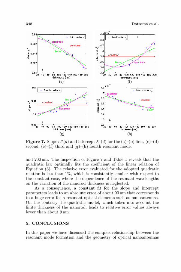
With the intent of exploring how αn(d) and λn0 (d) vary with
the thickness d for each resonant order mode, several nanoantennas,characterized by different values of thickness and length, have beenextensively simulated and analyzed. In Figure 7 each circle depictsthe evaluated slope αn(d) and the intercept λn
0 (d), by changing thethickness d, for each resonant order mode. From the inspection of thefigure, it is possible to claim that the slope and the intercept cannotbe considered constant when the thickness is varied.
In order to describe the slope and intercept behavior with respect
Progress In Electromagnetics Research B, Vol. 30, 2011 347
to the thickness variation, three different fitting orders, namelyconstant (K), linear (L) and quadratic (Q), have been employed. Therelative error is given by the following equation:
e =∑
d
λFDTD(d)− λres(d)λFDTD(d)
(4)
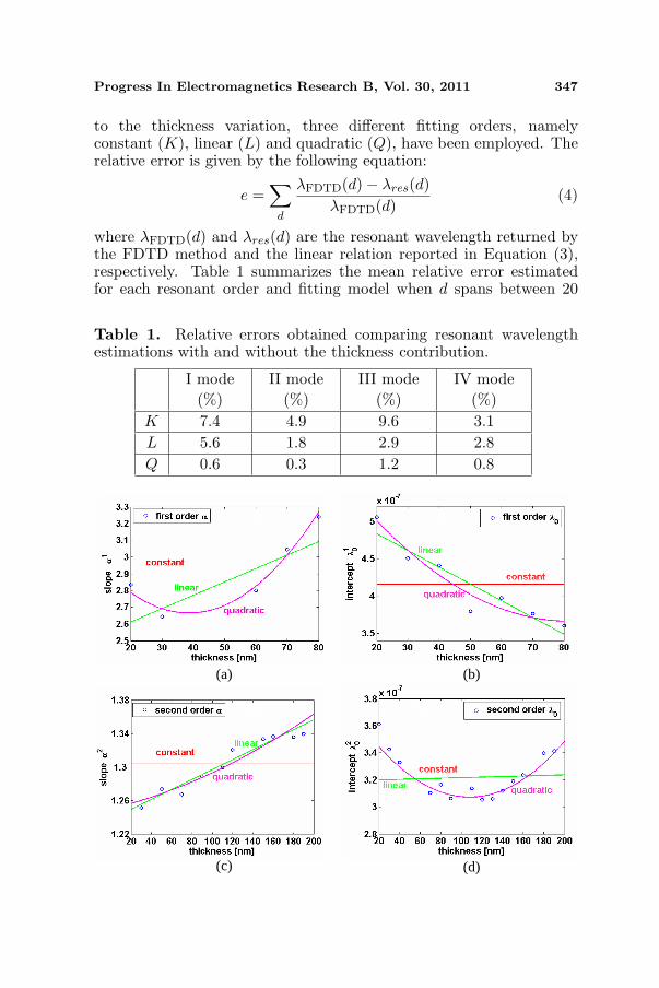
where λFDTD(d) and λres(d) are the resonant wavelength returned bythe FDTD method and the linear relation reported in Equation (3),respectively. Table 1 summarizes the mean relative error estimatedfor each resonant order and fitting model when d spans between 20
Table 1. Relative errors obtained comparing resonant wavelengthestimations with and without the thickness contribution.
I mode(%)
II mode(%)
III mode(%)
IV mode(%)
K 7.4 4.9 9.6 3.1L 5.6 1.8 2.9 2.8Q 0.6 0.3 1.2 0.8
(a) (b)
(c) (d)
348 Dattoma et al.
(e) (f)
(g) (h)
Figure 7. Slope αn(d) and intercept λn0 (d) for the (a)–(b) first, (c)–(d)
second, (e)–(f) third and (g)–(h) fourth resonant mode.
and 200 nm. The inspection of Figure 7 and Table 1 reveals that thequadratic law optimally fits the coefficient of the linear relation ofEquation (3). The relative error evaluated for the adopted quadraticrelation is less than 1%, which is consistently smaller with respect tothe constant case, where the dependence of the resonant wavelengthson the variation of the nanorod thickness is neglected.
As a consequence, a constant fit for the slope and interceptparameters leads to an absolute error of about 90 nm that correspondsto a huge error for a resonant optical elements such as nanoantennas.On the contrary the quadratic model, which takes into account thefinite thickness of the nanorod, leads to relative error values alwayslower than about 9 nm.
5. CONCLUSIONS
In this paper we have discussed the complex relationship between theresonant mode formation and the geometry of optical nanoantennas
Progress In Electromagnetics Research B, Vol. 30, 2011 349
having finite thickness. In particular we have shown that, dueto non-negligible thickness, gold nanorod antennas differ from RFcounterparts since the minima and maxima (nodes and anti-nodes) donot go to zero and show very intense peaks at the corners. Neverthelessthe mode profiles of the nanoantennas resemble the field distributionof the RF dipole antenna for all the analyzed resonant orders. Finally,the finite thickness of the nanorod in comparison with the lengthinduces a change of the predicted resonant wavelength. The obtainedresults show how the dependence of the resonant wavelength on thenanoantenna thickness is strictly important for the design and thefabrication of the resonant elements to be used in optical systems forquantum and on-chip communication.
ACKNOWLEDGMENT
The authors would like to acknowledge COST action MP0702 onTowards Functional Sub-Wavelength Photonic Structures.
REFERENCES
1. Novotny, L. and N. van Hulst, “Antennas for light,” NaturePhotonics, Vol. 5, 83–90, 2011.
2. Bharadwaj, P., B. Deutsch, and L. Novotny, “Optical antennas,”Advances in Optics and Photonics, Vol. 1, 438–483, 2009.
3. Park, Q.-H., “Optical antennas and plasmonics,” ContemporaryPhysics, Vol. 50, No. 2, 407–423, 2009.
4. Devilez, A., B. Stout, and N. Bonod, “Mode-balancing far-fieldcontrol of light localization in nanoantennas,” Phys. Rev. B,Vol. 81, 245128, 2010.
5. Marrocco, V., M. A. Vincenti, M. Grande, G. Calo, V. Petruzzelli,F. Prudenzano, and A. D’Orazio, “Field localization in Braggwaveguide assisted by metal layers,” J. of Optical Society ofAmerica B, Vol. 27, No. 4, 703–707, 2010.
6. Novotny, L. and S. J. Stranick, “Near-field optical microscopyand spectroscopy with pointed probes,” Ann. Rev. Phys. Chem.,Vol. 57, 303–331, 2006.
7. Farahani, J. N., D. W. Pohl, H. J. Eisler, and B. Hecht, “Singlequantum dot coupled to a scanning optical antenna: A tunablesuperemitter,” Phys. Rev. Lett., Vol. 95, No. 1, 017402, 2005.
8. Taminiau, T. H., R. J. Moerland, F. B. Segerink, L. Kuipers, andN. F. van Hulst, “λ/4 resonance of an optical monopole antenna
350 Dattoma et al.
probed by single molecule fluorescence,” Nano Letters, Vol. 7,No. 1, 28–33, 2007.
9. Krazinski, B. E., J. Radecki, and H. Radecka, “Surface plasmonresonance based biosensors for exploring the influence of alkaloidson aggregation of amyloid-β peptide,” Sensors, Vol. 11, 4030–4042, 2011.
10. Anker, J. N., W. P. Hall, O. Lyandres, N. C. Shah, J. Zhao,and R. P. van Duyne, “Biosensing with plasmonic nanosensors,”Nature Materials, Vol. 7, 442–453, 2008.
11. Cao, L., J. S. Park, P. Fan, B. Clemens, and M. L. Brongersma,“Resonant Germanium nanoantenna photodetectors,” NanoLetters, Vol. 10, 1229–1233, 2010.
12. Wu, W., A. Bonakdar, and H. Mohseni, “Plasmonic en-hanced quantum well infrared photodetector with high de-tectivity,” Applied Physics Letters, Vol. 96, 161107, 2010.doi:10.1063/1.3419885.
13. Cubukcu, E., E. A. Kort, K. B. Crozier, and F. Capasso,“Plasmonic laser antenna,” Applied Physics Letters, Vol. 89,093120, 2006.
14. Dey, D., J. Kohoutek, R. M. Gelfand, A. Bonakdar, andH. Mohseni, “Composite nano-antenna integrated with quantumcascade laser,” IEEE Photonics Technology Letters, Vol. 22,No. 21, 1580–1582, 2010.
15. Gao, H., K. Li, F. Kong, H. Xie, and J. Zhao, “Optimizing nano-optical antenna for the enhancement of spontaneous emission,”Progress In Electromagnetics Research, Vol. 104, 313–331, 2010.
16. Pillai, S. and M. A. Green, “Plasmonics for photovoltaicsapplications,” Solar Energy Materials & Solar Cells, Vol. 94,1481–1486, 2010.
17. Marrocco, V., R. Marani, M. Grande, G. Morea, G. Calo,V. Petruzzelli, and A. D’Orazio, “Modification of the scatteringof silver nanoparticles induced by Fabry-Perot resonances risingfrom a finite Si layer,” Journal of Optics, Vol. 13, 015004, 2011.
18. Marrocco, V., M. A. Vincenti, V. Petruzzelli, F. Prudenzano,and A. D’Orazio, “Efficient plasmonic nanostructures for thinfilm solar cells,” Photonics for Solar Energy Systems III,Proc. of SPIE, Vol. 7725, 2010. ISBN 9780819481986, doi:10.1117/12.862873.
19. Fumeaux, C., J. Alda, and G. D. Boreman, “Lithographicantennas at visible frequencies,” Optics Letters, Vol. 24, No. 22,1629–1631, 1999.
Progress In Electromagnetics Research B, Vol. 30, 2011 351
20. Simon, J. and F. J. Gonzales, “Nanoantennas for polarizationdivision multiplexing,” Electronics Letters, Vol. 47, No. 2, 120–121, 2011.
21. Taminiau, T. H., F. D. Stefani, F. B. Segerink, and N. F. vanHulst, “Optical antennas direct single-molecule emission,” NaturePhotonics, Vol. 2, 234–237, 2008.
22. Schuck, P. J., D. P. Fromm, A. Sundaramurthy, G. S. Kino,and W. E. Moerner, “Improving the mismatch between light andnanoscale objects with gold bowtie nanoantennas,” Phys. Rev.Lett., Vol. 94, 017402, 2005.
23. Alu, A. and N. Engheta, “Hertzian plasmonic nanodimer as anefficient optical nanoantenna,” Phys. Rev. B, Vol. 78, 195111,2008.
24. Bryant, G. W., F. J. G. de Abajo, and J. Aizpurua, “Mappingthe plasmon resonances of metallic nanoantennas,” Nano Letters,Vol. 8, 631–636, 2008.
25. Kosako, T., Y. Kadoya, and H. F. Hofmann, “Directional controlof light by a nano-optical Yagi-Uda antenna,” Nature Photonics,Vol. 4, 312–315, 2010.
26. Hofmann, H. F., T. Kosako, and Y. Kadoya, “Design parametersfor a nanooptical Yagi-Uda antenna,” New J. Phys., Vol. 9, 217–217, 2007.
27. Li, J., A. Salandrino, and N. Engheta, “Shaping light beams in thenanometer scale: A Yagi-Uda nanoantenna in the optical domain,”Phys. Rev. B, Vol. 76, 245403, 2007.
28. Kinkhabwala, A., Z. Yu, S. Fan, Y. Avlasevich, K. Mullen, andW. E. Moerner, “Large single-molecule fluorescence enhancementsproduced by a bowtie nanoantenna,” Nature Photon., Vol. 3, 654–657, 2009.
29. Guo, H., P. Meyrath, T. Zentgraf, N. Liu, L. Fu, H. Schweizer,and H. Giessen, “Optical resonances of bowtie slot antennas andtheir geometry and material dependence,” Optics Express, Vol. 16,7756–7766, 2008.
30. Kuehn, S., U. Hakanson, L. Rogobete, and V. Sandoghdar,“Enhancement of single-molecule fluorescence using a goldnanoparticle as an optical nanoantenna,” Phys. Rev. Lett., Vol. 97,017402, 2006.
31. Bharadwaj, P. and L. Novotny, “Spectral dependence of singlemolecule fluorescence enhancement,” Opt. Express, Vol. 15,14266–14274, 2007.
32. Gonzalez, F. J. and G. D. Boreman, “Comparison of dipole,
352 Dattoma et al.
bowtie, spiral and log-periodic IR antennas,” Infrared Physics &Technology, Vol. 46, No. 5, 418–428, 2005.
33. Fischer, H. and O. J. F. Martin, “Engineering the optical responseof plasmonic nanoantennas,” Opt. Express, Vol. 16, No. 12, 9144–9154, 2008.
34. Schuck, P., D. P. Fromm, A. Sundaramurthy, G. S. Kino, andW. E. Moerner, “Improving the mismatch between light andnanoscale objects with gold bowtie nanoantennas,” Phys. Rev.Lett., Vol. 94, 017402, 2005.
35. Biagioni, P., J. S. Huang, L. Du, M. Finazzi, and B. Hecht, “Crossresonant optical antenna,” Phys. Rev. Lett., Vol. 102, 256801,2009.
36. Centeno, A., J. Breeze, B. Ahmed, H. Reehal, and N. Alford,“Scattering of light into silicon by spherical and hemisphericalsilver nanoparticles,” Optics Letters, Vol. 35, No. 1, 75–78, 2010.
37. Centeno, A., F. Xie, and N. Alford, “Light absorption and fieldenhancement in two-dimensional arrays of closely spaced silvernanoparticles,” J. Opt. Soc. Am B, Vol. 28, No. 2, 325–329, 2011.
38. Zhang, M., X. Zhou, and Y. Fu, “Plasmonic resonance excitedextinction spectra of cross shaped Ag nanoparticles,” Plasmonics,Vol. 5, 355–366, 2010.
39. Marrocco, V., M. A. Vincenti, A. Mongiello, M. De Sario,V. Petruzzelli, F. Prudenzano, and A. D’Orazio, “Gold nanorodsin lineary modulated array,” Proc. of Metamaterials 2009, 3rd Int.Congr. On Advanced Electromagnetic Materials in Macrowavesand Optics, London, 2009.
40. Novotny, L., “Effective wavelength scaling for optical antennas,”Phys. Rev. Lett., Vol. 98, 266802, 2007.
41. Alu, A. and N. Engheta, “Input impedance, nanocircuit loading,and radiation tuning of optical nanoantennas,” Phys. Rev. Lett.,Vol. 101, 043901, 2008.
42. Locatelli, A., “Analysis of the optical properties of wire antennaswith displaced terminals,” Opt. Express, Vol. 18, No. 9, 9504–9510,2010.
43. Ginzburg, P. and M. Orenstein, “Plasmonic transmission lines:From micro to nano scale with λ/4 impedance matching,” Opt.Express, Vol. 15, 6762–6767, 2007.
44. Zhao, Y., N. Engheta, and A. Alu, “Effects of shape and loading ofoptical nanoantennas on its sensitivity and radiation properties,”Journal of Optical Society of America B, 2011.
45. Balanis, C., Antenna Theory: Analysis and Design, John Wiley
Progress In Electromagnetics Research B, Vol. 30, 2011 353
and Sons, Inc., New York, NY, 1996.46. Bean, J. A., B. A. Slovick, and G. D. Boreman, “Influence of
substrate configuration on the angular response pattern of infraredantennas,” Opt. Express, Vol. 18, No. 21, 21705–21713, 2010.
47. McMahon, J. M., JFDTD2D, http: www.thecomputationalphysici-st.com, 2009.
48. Veronis, G. and S. Fan, “Subwavelength plasmonic waveguidestructures based on slots in thin metal films,” Proc. of SPIE,Vol. 6123, 2006.
49. Stewart, M. E., N. H. Mack, V. Malyarchuk, J. A. N. T. Soares,T. W. Lee, S. K. Gray, R. G. Nuzzo, and J. A. Rogers,“Quantitative multispectral biosensing and 1D imaging usingquasi-3D plasmonic crystals,” Proc. Nat. Acad. Sci., Vol. 103,17143, USA, 2006.
50. Palik, E. D., Handbook of Optical Constants of Solids, AcademicPress, San Diego, CA, 1998.
51. Pezzagna, S., J. Brault, M. de Micheli, P. Vennegues, A. D. Wieck,and J. Massies, “GaN, a new material for integrated nonlinearoptics,” Proc. of ECIO 2007, Copenhagen, Denmark, Apr. 25–27,2007.
52. McMahon, J. M., J. Henzie, T. W. Odom, G. C. Schatz, andS. K. Gray, “Tailoring the sensing capabilities of nanohole arraysin gold films with Rayleigh anomaly-surface plasmon polaritons,”Opt. Express, Vol. 15, 18119, 2007.
53. Wang, F. and Y. R. Shen, “General properties of local plasmonsin metal nanostructures,” Phys. Rev. Lett., Vol. 97, 206806, 2006.
54. Bozhevolnyi, S. I. and T. Sondergaard, “General propertiesof slow-plasmon resonant nanostructures: Nanoantennas andresonators,” Opt. Express, Vol. 15, 10869, 2006.
55. Maier, S. A., Plasmonics: Fundamentals and Applications,Springer Science, New York, NY, 2007.
56. Barnes, W. L., A. Dereux, and T. Ebbesen, “Surface plasmonsubwavelength,” Optics Nature, Vol. 424, 824, 2003.
57. Boriskina, S. V. and L. Dal Negro, “Multiple-wavelengthplasmonic,” Nanoantennas Opt. Lett., Vol. 35, 538, 2010.
58. Grenuche, P., S. Cherukulappurath, T. H. Taminiau, N. F. VanHulst, and R. Quidant, “Spectroscopic mode mapping of resonantplasmon nanoantennas,” Phys. Rev. Lett., Vol. 101, 116805, 2008.