Embed Size (px)
Citation preview

Resistive Random Access Memory (RRAM)From Devices to Array Architectures

iii
Synthesis Lectures on Emerging Engineering Technology
Kris Iniewski, Redlen Technologies, Inc.
Resistive Random Access Memory (RRAM): From Devices to Array ArchitecturesShimeng YuMarch 2016
The Digital Revolution Bob MerrittFebruary 2016
Compound Semiconductor Materials and DevicesZhaojun Liu, Tongde Huang, Qiang Li, Xing Lu, Xinbo ZouFebruary 2016
New Prospects of Integrating Low Substrate Temperatures with Scaling-Sustained Device Archi-tectural InnovationNabil Shovon Ashraf, Shawon Alam, Mohaiminul AlamFebruary 2015
Advances in Reflectometric Sensing for Industrial ApplicationsAndrea Cataldo, Egidio De Benedetto, and Giuseppe CannazzaJanuary 2016
Sustaining Moore’s Law: Uncertainty Leading to a Certainty of IoT RevolutionApek MulaySeptember 2015
Copyright © 2016 by Morgan & Claypool
All rights reserved. No part of this publication may be reproduced, stored in a retrieval system, or transmitted inany form or by any means—electronic, mechanical, photocopy, recording, or any other except for brief quota-tions in printed reviews, without the prior permission of the publisher.
Resistive Random Access Memory (RRAM): From Devices to Array Architectures Shimeng Yuwww.morganclaypool.com
ISBN: 9781627059299 printISBN: 9781627059305 ebook
DOI 10.2200/S00681ED1V01Y201510EET006
A Publication in the Morgan & Claypool Publishers seriesSYNTHESIS LECTURES ON EMERGINT ENGINEERING TECHNOLOGIES, #6Series Editors: Kris Iniewski, Redlen Technologies, Inc.
Series ISSN 2381-1412 Print 2381-1439 Electronic
Resistive Random Access Memory (RRAM)From Devices to Array Architectures
Shimeng YuArizona State University
SYNTHESIS LECTURES ON EMERGING ENGINEERING TECHNOLOGIES #6
M&C MORGAN & CLAYPOOL PUBLISHERS
vi
ABSTRACTRRAM technology has made significant progress in the past decade as a competitive candidate for the next generation non-volatile memory (NVM). This lecture is a comprehensive tutorial of metal oxide-based RRAM technology from device fabrication to array architecture design. State-of-the-art RRAM device performances, characterization, and modeling techniques are summarized, and the design considerations of the RRAM integration to large-scale array with peripheral circuits are discussed. Chapter 2 introduces the RRAM device fabrication techniques and methods to elimi-nate the forming process, and will show its scalability down to sub-10 nm regime. Then the device performances such as programming speed, variability control, and multi-level operation are pre-sented, and finally the reliability issues such as cycling endurance and data retention are discussed. Chapter 3 discusses the RRAM physical mechanism, and the materials characterization techniques to observe the conductive filaments and the electrical characterization techniques to study the electronic conduction processes. It also presents the numerical device modeling techniques for simulating the evolution of the conductive filaments as well as the compact device modeling tech-niques for circuit-level design. Chapter 4 discusses the two common RRAM array architectures for large-scale integration: one-transistor-one-resistor (1T1R) and cross-point architecture with selector. The write/read schemes are presented and the peripheral circuitry design considerations are discussed. Finally, a 3D integration approach is introduced for building ultra-high density RRAM array. Chapter 5 is a brief summary and will give an outlook for RRAM’s potential novel applica-tions beyond the NVM applications.
KEYWORDSRRAM, ReRAM, resistive switching, non-volatile memory
vii
Contents1 Introduction to RRAM Technology . . . . . . . . . . . . . . . . . . . . . . . . . . . . . . . . . . . . . 1
1.1 Overview of Emerging Memory Technologies . . . . . . . . . . . . . . . . . . . . . . . . 11.2 RRAM Basics . . . . . . . . . . . . . . . . . . . . . . . . . . . . . . . . . . . . . . . . . . . . . . . . . 31.3 Recent Research and Development of RRAM Technology . . . . . . . . . . . . . . 7
2 RRAM Device Fabrication and Performances . . . . . . . . . . . . . . . . . . . . . . . . . . . . . 92.1 Device Fabrication: Forming-Free and Scalability . . . . . . . . . . . . . . . . . . . . . . 92.2 Device Performances . . . . . . . . . . . . . . . . . . . . . . . . . . . . . . . . . . . . . . . . . . . 122.3 Device Reliability . . . . . . . . . . . . . . . . . . . . . . . . . . . . . . . . . . . . . . . . . . . . . 15
3 RRAM Characterization and Modeling . . . . . . . . . . . . . . . . . . . . . . . . . . . . . . . . . 213.1 Overview of RRAM Physical Mechanism . . . . . . . . . . . . . . . . . . . . . . . . . . 213.2 Materials and Electrical Characterization . . . . . . . . . . . . . . . . . . . . . . . . . . 223.3 Numerical Modeling using Kinetic Monte-Carlo Method . . . . . . . . . . . . . . 273.4 Compact Modeling for SPICE Simulation . . . . . . . . . . . . . . . . . . . . . . . . . . 31
4 RRAM Array Architecture . . . . . . . . . . . . . . . . . . . . . . . . . . . . . . . . . . . . . . . . . . . 354.1 1T1R Array . . . . . . . . . . . . . . . . . . . . . . . . . . . . . . . . . . . . . . . . . . . . . . . . . . 354.2 Cross-point Array . . . . . . . . . . . . . . . . . . . . . . . . . . . . . . . . . . . . . . . . . . . . . 384.3 Selector Device . . . . . . . . . . . . . . . . . . . . . . . . . . . . . . . . . . . . . . . . . . . . . . . 434.4 Peripheral Circuits Design . . . . . . . . . . . . . . . . . . . . . . . . . . . . . . . . . . . . . . . 474.5 3D Integration . . . . . . . . . . . . . . . . . . . . . . . . . . . . . . . . . . . . . . . . . . . . . . . 51
5 Outlook for RRAM’s Applications . . . . . . . . . . . . . . . . . . . . . . . . . . . . . . . . . . . . 55
Bibliography . . . . . . . . . . . . . . . . . . . . . . . . . . . . . . . . . . . . . . . . . . . . . . . . . . . . . . . 57
Author Biography . . . . . . . . . . . . . . . . . . . . . . . . . . . . . . . . . . . . . . . . . . . . . . . . . . . 71

1
CHAPTER 1
Introduction to RRAM Technology
1.1 OVERVIEW OF EMERGING MEMORY TECHNOLOGIESThe functionality and performance of today’s computing system are increasingly dependent on the characteristics of the memory sub-system. The memory sub-system has a well-known hierarchy: From top layers to bottom layers, SRAM, DRAM, and FLASH are the mainstream memory technologies serving as cache, main memory, and solid-state-drive (SSD), respectively. Moving up the hierarchy, the memory write/read latency decreases. Moving down the hierarchy, the memory capacity increases. All these mainstream memory technologies are based on the charge storage mechanism: SRAM stores the charge at the storage nodes of the cross-coupled inverters, DRAM stores the charge at the cell capacitor, and FLASH stores the charge at the floating gate of the transistor. All these charge-based memories are facing challenges to be scaled down to 10 nm node or beyond, due to the easy loss of the stored charge at nanoscale, resulting in the degradation of the performance, reliability, and noise margin, etc. In this context, emerging memory technologies that are non-charge based are actively under research and development in the industry, with the hope to revolutionize the memory hierarchy [1].
The ideal characteristics for a memory device include fast write/read speed (<ns), low opera-tion voltage (<1 V), low energy consumption (~fJ/bit for write/read), long data retention time (>10 years), long write/read cycling endurance (>1017 cycles), and excellent scalability (<10 nm). Never-theless, it is almost impossible to satisfy these ideal characteristics in a single “universal” memory device. Several emerging non-volatile memory (NVM) technologies have been pursued toward to achieving part of these ideal characteristics. The emerging NVM candidates are spin-transfer-torque magnetoresistive random access memory (STT-MRAM) [2], phase change random access memory (PCRAM) [3], and resistive random access memory (RRAM) [4]. These emerging NVM technologies share some common features: they are non-volatile two-terminal devices, and they differentiate their states by the switching between a high resistance state (HRS, or off-state) and a low resistance state (LRS, or on-state). The transition between the two states can be triggered by electrical inputs. However, the detailed switching physics is quite different for different memories: STT-MRAM relies on difference in resistance between the parallel configuration (corresponding to LRS) and the anti-parallel configuration (corresponding to HRS) of two ferromagnetic layers separated by a thin tunneling insulator layer; PCRAM relies on chalcogenide material to switch
2 1. INTRODUCTION TO RRAM TECHNOLOGY
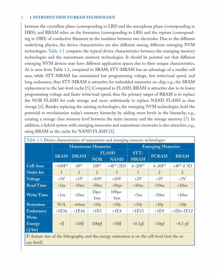
between the crystalline phase (corresponding to LRS) and the amorphous phase (corresponding to HRS); and RRAM relies on the formation (corresponding to LRS) and the rupture (correspond-ing to HRS) of conductive filaments in the insulator between two electrodes. Due to the different underlying physics, the device characteristics are also different among different emerging NVM technologies. Table 1.1 compares the typical device characteristics between the emerging memory technologies and the mainstream memory technologies. It should be pointed out that different emerging NVM devices may have different application spaces due to their unique characteristics. As is seen from Table 1.1, compared to SRAM, STT-MRAM has an advantage of a smaller cell area, while STT-MRAM has maintained low programming voltage, fast write/read speed, and long endurance, thus STT-MRAM is attractive for embedded memories on chip, e.g., the SRAM replacement in the last-level cache [5]. Compared to FLASH, RRAM is attractive due to its lower programming voltage and faster write/read speed, thus the primary target of RRAM is to replace the NOR FLASH for code storage and more ambitiously to replace NAND FLASH as data storage [6]. Besides replacing the existing technologies, the emerging NVM technologies hold the potential to revolutionize today’s memory hierarchy by adding more levels in the hierarchy, e.g., creating a storage class memory level between the main memory and the storage memory [7]. In addition, a hybrid system with emerging memories and mainstream memories is also attractive, e.g., using RRAM as the cache for NAND FLASH [8].
Table 1.1: Device characteristics of mainstream and emerging memory technologiesMainstream Memories Emerging Memories
SRAM DRAMFLASH STT-
MRAMPCRAM RRAM
NOR NANDCell Area >100F2 6F2 10F2 <4F2 (3D) 6~20F2 4~20F2 <4F2 if 3DMulti-bit 1 1 2 3 1 2 2Voltage <1V <1V >10V >10V <2V <3V <3VRead Time ~1ns ~10ns ~50ns ~10µs <10ns <10ns <10ns
Write Time ~1ns ~10ns10µs-1ms
100µs-1ms
<5ns ~50ns <10ns
Retention N/A ~64ms >10y >10y >10y >10y >10yEndurance >1E16 >1E16 >1E5 >1E4 >1E15 >1E9 >1E6~1E12Write Energy ( J/bit)
~fJ ~10fJ 100pJ ~10fJ ~0.1pJ ~10pJ ~0.1 pJ
F: feature size of the lithography, and the energy estimation is on the cell-level (not the ar-ray-level)
3
1.2 RRAM BASICS The resistive switching phenomenon where the resistance of insulators such as metal oxides changes when a large voltage is applied was firstly reported in the 1960s [9]. The recent revival on the re-sistive switching can be traced back to the discovery of hysteresis I-V characteristics in perovskite oxides such as Pr0.7Ca0.3MnO3 [10], SrZrO3 [11], SrTiO3 [12], etc., in the late 1990s and the early 2000s. Since Samsung demonstrated NiO RRAM array integrated with the 180 nm silicon CMOS technology in 2004 [13], research activities have been blooming with demonstrations of resistive switching in various binary oxides1 such as NiO [14], TiOx [15], CuOx [16], ZrOx [17], ZnOx [18], HfOx [19], TaOx [20], AlOx [21], etc., because of the simplicity of the materials and good compatibility with silicon CMOS fabrication process. Later in 2008, HP Labs made the connection of the resistive devices to the theoretical concept of memristor [22].2
Generally speaking, there are two types of RRAM. The first type is based on the conductive filaments consisting of oxygen vacancies, which is typically referred to as oxide-based RRAM; the second type is based on the conductive filaments consisting of metal atoms, which is also called conductive-bridge RAM (CBRAM). CBRAM relies on the fast-diffusive Ag or Cu ions migration into the oxide (or chalcogenide) to form a conductive bridge. Despite different underlying switch-ing physics, these two types share a lot of common device characteristics and the array architecture design considerations are very similar. In this lecture, we focus on the first type: oxygen vacancy based oxide RRAM.3 In literature, there are a few comprehensive reviews on the oxide RRAM [23, 24, 25, 4]. For the CBRAM, refer to the review [26].
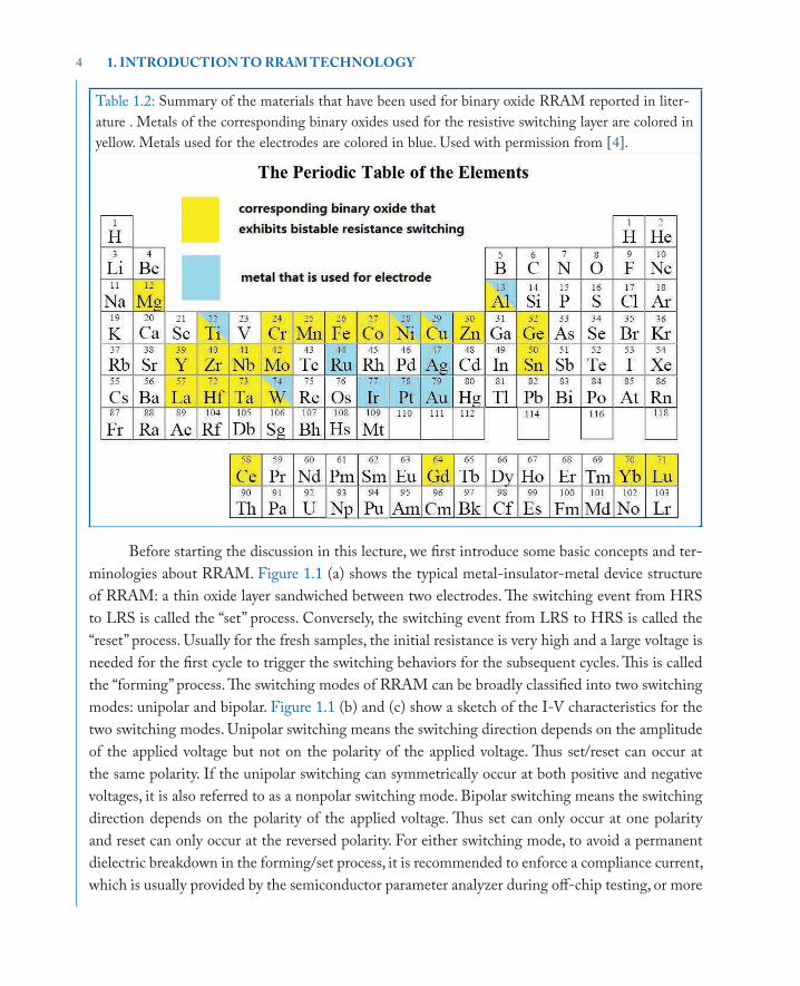
So far, tens of binary oxides have been found to exhibit resistive switching behavior. Most of them are transition metal oxides, and some are lanthanide series metal oxides. The materials for the resistive switching oxide layer and the electrodes reported in literature are summarized in Table 1.2. Besides metals, conductive nitrides, e.g., TiN, TaN, are also commonly used as electrode materials.
1 These binary oxides that show resistive switching are often non-stoichiometric, thus subscript “x” is used for the oxygen composition in this book.
2 To unify the terminology and emphasize the technology development, RRAM is used instead of memristor in this book.
3 If not specifically noted, the term “RRAM” refers to the binary oxide memory involving oxygen vacancies in this book.
RRAM BASICS
4 1. INTRODUCTION TO RRAM TECHNOLOGY
Table 1.2: Summary of the materials that have been used for binary oxide RRAM reported in liter-ature . Metals of the corresponding binary oxides used for the resistive switching layer are colored in yellow. Metals used for the electrodes are colored in blue. Used with permission from [4].
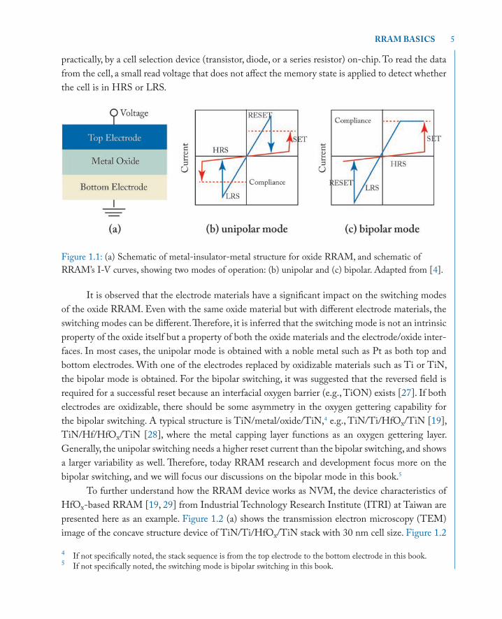
Before starting the discussion in this lecture, we first introduce some basic concepts and ter-minologies about RRAM. Figure 1.1 (a) shows the typical metal-insulator-metal device structure of RRAM: a thin oxide layer sandwiched between two electrodes. The switching event from HRS to LRS is called the “set” process. Conversely, the switching event from LRS to HRS is called the “reset” process. Usually for the fresh samples, the initial resistance is very high and a large voltage is needed for the first cycle to trigger the switching behaviors for the subsequent cycles. This is called the “forming” process. The switching modes of RRAM can be broadly classified into two switching modes: unipolar and bipolar. Figure 1.1 (b) and (c) show a sketch of the I-V characteristics for the two switching modes. Unipolar switching means the switching direction depends on the amplitude of the applied voltage but not on the polarity of the applied voltage. Thus set/reset can occur at the same polarity. If the unipolar switching can symmetrically occur at both positive and negative voltages, it is also referred to as a nonpolar switching mode. Bipolar switching means the switching direction depends on the polarity of the applied voltage. Thus set can only occur at one polarity and reset can only occur at the reversed polarity. For either switching mode, to avoid a permanent dielectric breakdown in the forming/set process, it is recommended to enforce a compliance current, which is usually provided by the semiconductor parameter analyzer during off-chip testing, or more
5
practically, by a cell selection device (transistor, diode, or a series resistor) on-chip. To read the data from the cell, a small read voltage that does not affect the memory state is applied to detect whether the cell is in HRS or LRS.
Figure 1.1: (a) Schematic of metal-insulator-metal structure for oxide RRAM, and schematic of RRAM’s I-V curves, showing two modes of operation: (b) unipolar and (c) bipolar. Adapted from [4].
It is observed that the electrode materials have a significant impact on the switching modes of the oxide RRAM. Even with the same oxide material but with different electrode materials, the switching modes can be different. Therefore, it is inferred that the switching mode is not an intrinsic property of the oxide itself but a property of both the oxide materials and the electrode/oxide inter-faces. In most cases, the unipolar mode is obtained with a noble metal such as Pt as both top and bottom electrodes. With one of the electrodes replaced by oxidizable materials such as Ti or TiN, the bipolar mode is obtained. For the bipolar switching, it was suggested that the reversed field is required for a successful reset because an interfacial oxygen barrier (e.g., TiON) exists [27]. If both electrodes are oxidizable, there should be some asymmetry in the oxygen gettering capability for the bipolar switching. A typical structure is TiN/metal/oxide/TiN,4 e.g., TiN/Ti/HfOx/TiN [19], TiN/Hf/HfOx/TiN [28], where the metal capping layer functions as an oxygen gettering layer. Generally, the unipolar switching needs a higher reset current than the bipolar switching, and shows a larger variability as well. Therefore, today RRAM research and development focus more on the bipolar switching, and we will focus our discussions on the bipolar mode in this book.5
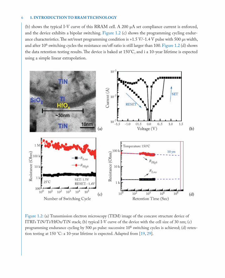
To further understand how the RRAM device works as NVM, the device characteristics of HfOx-based RRAM [19, 29] from Industrial Technology Research Institute (ITRI) at Taiwan are presented here as an example. Figure 1.2 (a) shows the transmission electron microscopy (TEM) image of the concave structure device of TiN/Ti/HfOx/TiN stack with 30 nm cell size. Figure 1.2
4 If not specifically noted, the stack sequence is from the top electrode to the bottom electrode in this book.5 If not specifically noted, the switching mode is bipolar switching in this book.
RRAM BASICS
6 1. INTRODUCTION TO RRAM TECHNOLOGY
(b) shows the typical I-V curve of this RRAM cell. A 200 µA set compliance current is enforced, and the device exhibits a bipolar switching. Figure 1.2 (c) shows the programming cycling endur-ance characteristics. The set/reset programming condition is +1.5 V/-1.4 V pulse with 500 µs width, and after 106 switching cycles the resistance on/off ratio is still larger than 100. Figure 1.2 (d) shows the data retention testing results. The device is baked at 150°C, and i a 10-year lifetime is expected using a simple linear extrapolation.
Figure 1.2: (a) Transmission electron microscopy (TEM) image of the concave structure device of ITRI’s TiN/Ti/HfOx/TiN stack; (b) typical I-V curve of the device with the cell size of 30 nm; (c) programming endurance cycling by 500 µs pulse: successive 106 switching cycles is achieved; (d) reten-tion testing at 150 °C: a 10-year lifetime is expected. Adapted from [19, 29].
7
1.3 RECENT RESEARCH AND DEVELOPMENT OF RRAM TECHNOLOGY
The development of oxide RRAM has progressed rapidly in the past decade. In particular, binary oxides that use materials that are compatible to the silicon CMOS fabrication process have seen intense research and development in the industry. The early RRAM devices in the mid-2000s had large device area (>>µm2), large programming current (~mA), long programming time (>µs), low endurance (<103 cycles), and required a large forming voltage (~10 V). Today, many of these defi-ciencies have been overcome. Device sizes down to 10 nm or below have been demonstrated [28, 30], programming current is now in the order of tens of µA or a few µA, programming speed is in the order of tens of ns or a few ns, programming endurance cycles are typically larger than 106 with a record up to 1012 [31], retention time is >3,000 h at 150°C and extrapolated to be more than 10 years at 85°C [20], and the forming process can be eliminated by shrinking the oxide thickness [32] or other oxide stack engineering strategies. Most of these good characteristics were reported in HfOx or TaOx systems. Demonstrations of 2-bit and 3-bit multi-level operation have also been made [33, 34]. Chip-level RRAM array macro from 4 Mb to 32 Gb capacity with peripheral cir-cuitry have been demonstrated by industry as well [35, 36, 37], showing that RRAM is a viable NVM technology for practical applications.
This book is organized as follows. Chapter 2 will discuss the RRAM device fabrication techniques and methods to eliminate the forming process, and will show its scalability down to sub-10 nm regime. Then the device performances such as programming speed, variability control, and multi-level operation will be presented, and finally the reliability issues such as cycling endur-ance and data retention will be discussed. Chapter 3 will discuss the RRAM physical mechanism, the materials characterization techniques to observe the conductive filaments, and the electrical characterization techniques to study the electronic conduction processes. It will also present the nu-merical device modeling techniques for simulating the evolution of the conductive filaments as well as the compact device modeling techniques for circuit-level design. Chapter 4 will discuss the two common RRAM array architectures for large-scale integration: one-transistor-one-resistor (1T1R) and cross-point architecture with selector. The write/read schemes are presented and the peripheral circuitry design considerations are discussed. Finally, a 3D integration approach is introduced for building ultra-high density RRAM array. Chapter 5 is a brief summary and will give an outlook for RRAM’s potential novel applications beyond the NVM applications.
RECENT RESEARCH AND DEVELOPMENT OF RRAM TECHNOLOGY