Embed Size (px)
Citation preview

1IXYS reserves the right to change limits, test conditions and dimensions
Contents Page
Symbols and Definitions 2Nomenclature 2General Informations for Chips 3Assembly Instructions 4FRED, Rectifier Diode and Thyristor Chips in Planar Design 5
IGBT ChipsVCES IC
G-Series, Low VCE(sat) B2 Types 600 ...1200 V 7 ... 20 A 6G-Series, Fast C2 Types 600 V 7 ... 20 A 6S-Series, SCSOA Capability, Fast Types 600 V 10 ... 20 A 6E-Series, Improved NPT³ technology 1200 ... 1700 V 20 ... 150 A 7
MOSFET ChipsVDSS RDS(on)
HiPerFETTM Power MOSFET 70 ...1200 V 0.005 ... 4.5 Ω 8-10PolarHT/HVTM Power MOSFET 55 ... 600 V 0.015 ... 0.135 Ω 11PolarHT/HVTM HiPerFET Power MOSFET 100 ... 600 V 0.0075 ... 0.74 Ω 12-14N-Channel Depletion Mode MOSFET 500 ...1000 V 30 ... 110 Ω 15P-Channel Power MOSFET -100 ...-600 V 0.06 ... 1.2 Ω 15
Chip outlines 16-23
Bipolar ChipsVRRM / VDRM IF(AV)M / IT(AV)M
Rectifier Diodes 800 ... 2200 V 12 ... 788 A 24-25FREDs 200 ... 1200 V 8 ... 244 A 26-28Low Leakage FREDs 200 ... 1200 V 9 ... 148 A 29-30SONIC-FRDTM Diodes 600 ... 1800 V 12 ... 150 A 31-32GaAs Schottky Diodes 100 ... 300 V 3.5 ... 25 A 33-34Schottky Diodes 8 ... 200 V 28 ... 145 A 35-38Phase Control Thyristors 800 ... 2200 V 15 ... 540 A 39-40Fast Rectifier Diodes 1600 ... 1800 V 10 ... 26 A 41
Direct Copper Bonded (DCB) Ceramic Substrates
What is DCB? 42
DCB Specification 43
www.ixys.com

2 © 2008 IXYS All rights reserved
Registration No.:OHSAS 18001:
001947 OH
Symbols and Definitions Cies Input capacitance of IGBT Ciss Input capacitance of MOSFET -di/dt Rate of decrease of forward current IC DC collector current ID Drain current IF Forward current of diode IF(AV)M Maximum average forward current at specified Th
IFSM Peak one cycle surge forward current IGT Gate trigger current IR Reverse current IRM Maximum peak recovery current IT Forward current of thyristor IT(AV)M Maximum average on-state current of a thyristor
at specified Th ITSM Maximum surge current of a thyristor RDS(on) Static drain-source on-state resistance Rthjc Thermal resistance junction to case rT Slope resistance of a thyristor or diode
(for power loss calculations) Tcase Case temperature Th Heatsink temperature tfi Current fall time with inductive load Tj, T(vj) Junction temperature Tjm, T(vj)m Maximum junction temperature trr Reverse recovery time of a diode VCE(sat) Collector-emitter saturation voltage VCES Maximum collector-emitter voltage VDRM Maximum repetitive forward blocking
voltage of thyristor VDSS Drain-source break-down voltage VF Forward voltage of diode VR Reverse voltage VRRM Maximum peak reverse voltage of thyristor or
diode VT On-state voltage of thyristor VT0 Threshold voltage of thyristors or diodes (for
power loss calculation only)
Chip and DCB Ceramic Substrates catalogueEdition 2008
Published by IXYS Semiconductor GmbHMarketing CommunicationsEdisonstraße 15, D-68623 Lampertheim
© IXYS Semiconductor GmbH All Rights reserved
As far as patents or other rights of third parties are concerned, liability is onlyassumed for chips and DCB parts per se, not for applications, processes andcircuits implemented with components or assemblies. Terms of delivery and theright to change design or specifications are reserved.
NomenclatureIGBT and MOSFET DiscreteIXSD 40N60A (Example)IX IXYS
Die technologyE NPT3 IGBTF HiPerFETTM Power MOSFETG Fast IGBTS IGBT with SCSOA capabilityT Standard Power MOSFET
D Unassembled chip (die)
40 Current rating, 40 = 40 A
N N-channel typeP P-channel type
60 Voltage class, 60 = 600 V
xxMOSFET
A Prime RDS(on) for standard MOSFETQ Low gate charge dieQ2 Low gate charge die, 2nd generationP PolarHT/HV Power MOSFETL Linear Mode MOSFET
IGBT-- No letter, low VCE(sat)
A Or A2, std speed typeB Or B2, high speed typeC Or C2, very high speed type
W-CWP 55-12/18 (Thyristor Example)
W Package type
C Chip functionC = Silicon phase control thyristor
W Unassembled chip
P Process designatorP = Planar passivated chip cathode on top
55 Current rating value of one chip in A
12/18 Voltage class, 12/18 = 1200 up to 1800 V
Diode and Thyristor ChipsC-DWEP 69-12 (Diode Example)
C Package type
D Chip functionD = Silicon rectifier diode
W Unassembled chip
EP Process designatorEP = Epitaxial rectifier diodeN = Rectifier diode, cathode on topP = Rectifier diode, anode on topFN = Fast Rectifier diode, cathode on topFP = Fast Rectifier diode, anode on top
69 Current rating value of one chip in A
-12 Voltage class, 12 = 1200 VRegistration No.:ISO/TS 16949:
001947 TS2
Registration No.:ISO 14001:001947 UM

3IXYS reserves the right to change limits, test conditions and dimensions
General Informations for Chips
When mounting Power Semiconductor chips to a header, ceramic substrate or hybrid thick film circuit, the solder system and the chipattach process are very important to the reliability and performance of the final product. This brochure provides several guidelinesthat describe recommended chip attachment procedures. These methods have been used successfully for many years at IXYS.
Available Packaging OptionsIXYS offers various options.Please order from one of the following possibilities:
Packaging Options Delivery form
C-...* Chips in tray (Waffle Pack); Electrically tested
T-...* Chips in wafer, unsawed; Bipolar = 5" (125 mm∅) wafer;or 6 " (150 mm∅)
W-...* Chips in wafer on foil, sawed; Bipolar = 5" (125 mm∅) wafer;or 6 " (150 mm∅)
...* must be amended by the exact chip type designation.
Package, Storage and HandlingChips should be transported in their original containers. All chip transfer to other containers or for assembly should be done only withrubber-tipped vacuum pencils. Contact with human skin (or with a tool that has been touched by hand) leaves an oily residue that mayadversely impact subsequent chip attach or reliability.
At temperatures below 104°F (40°C), there is no limitation on storage time for chips in sealed original packages. Chips removed fromoriginal packages should be assembled immediately. The wetting ability of the contact metallization with solder can be preserved bystorage in a clean and dry nitrogen atmosphere.
The IGBT and MOSFET Chips are electrostatic discharge (ESD) sensitive. Normal ESD precautions for handling must be observed.Prior to chip attach, all testing and handling of the chips must be done at ESD safe work stations according to DIN IEC 47(CO) 701.Ionized air blowers are recommended for added ESD protection.
Contamination of the chips degrades the assembly results.Finger prints, dust or oily deposits on the surface of the chips have to beabsolutely avoided.Rough mechanical treatment can cause damage to the chip.
Electrical TestsThe electrical properties listed in the data sheet presume correctly assembled chips. Testing of non-assembled chips requires thefollowing precautions:
• High currents have to be supplied homogeneously to the whole metallized contact area.
• Kelvin probes must be used to test voltages at high currents
• Applying the full specified blocking or reverse voltage may cause arcing across the glass passivated junction termination,because the electrical field on top of the passivation glass causes ionization of the surrounding air. This phenomenon can beavoided by using inert fluids or by increasing the pressure of the gas surrounding the chip to values above 30 psig (2 bars).
General Rules for AssemblyThe linear thermal expansion coefficient of silicon is very small compared to usual contact metals. If a large area metallized siliconchip is directly soldered to a metal like copper, enormous shear stress is caused by temperature changes (e.g. when cooling down fromthe solder temperature or by heating during working conditions) which can disrupt the solder mountdown.
If it is found that larger chips are cracking during mountdown or in the application, then the use of a low thermal expansion coefficientbuffer layer, e.g. tungsten, molybdenum or Trimetal®, for strain relief should be considered. An alternative solution is to soft-solder theselarger chips to DCB ceramic substrates because of their matching thermal expansion coefficients.
Electrically tested, rejects are inked
Electrically tested, rejects are inked

4 © 2008 IXYS All rights reserved
MOS/IGBT ChipsRecommended Solder System
IXYS recommends a soft solder chip attach using a solder composition of 92.5 % Pb, 5 % Sn and 2.5 % Ag. The maximum chip attachtemperature is 460°C for MOSFET and 360°C for HiPerFETTM and IGBT.
Wire Bonding
It is recommended to use wire of diameter not greater than 0.38 mm (0.015") for bonding to the source emitter and gate pads. Multiplewires should be used in place of thicker wire to handle high drain or emitter currents. See tables for number of recommended wirebonds. For smaller gate pads, 0.15 mm diameter wire is recommended.
Thermal Response Testing
To assure good chip attach processing, thermal response testing per MIL STD 750, Method 3161 or equivalent should be performed.
Bipolar ChipsAssembling
IXYS bipolar semiconductor chips have a soft-solderable, multi-layer metallization (Ti/Ni/Ag) on the bottom side and, on top, eitherthe same metallization scheme or an alumunium layer sufficiently thick for ultrasonic bonding. Note that the last layer of metal forsoldering is pure silver.
Regardless of their type all chips possess the same glass passivated junction termination system on top of the chip. For that reasonthey can be easily chip bonded or they can all be simply soldered to a flat contacting electrode in accordance to the General Rules onPage 3. All kinds of the usual soft solders with melting points below 660°F (350°C) can be used thanks to their pure silver top metal.Solders with high melting points are preferable due to their better power cycling capability, i.e. they are more resistant to thermalfatigue.
Soldering temperature should not exceed 750°F (400°C). The maximum temperature should not be applied for more than fiveminutes.
As already mentioned above the electrical properties quoted in the data sheets can only be obtained with properly assembled chips.This is only possible when all contact materials to be soldered together are well wetted and the solder is practically free of voids.
A simple means to achieve good solder connections is to use a belt furnace running with a process gas containing at least 10 %Hydrogen in Nitrogen.Other approved methods are also allowed, provided that the above mentioned temperature-time-limits are not exceeded andtemperature shocks above 930°F/min (500 K/min) are avoided.
We do not recommend the use of fluxes for soldering!
Ultrasonic Wire Bonding
Chips provided with a thick aluminium layer are designed for ultrasonic wire bonding. Wire diameters up to 500 µm can be useddependent on chip types. Setting wires in parallel and application of stitch bonding lead to surge current ratings comparable tosoldered chips.
Coating
Although the chips are glass passivated, they must be protected against arcing and environmental influences. The coating materialthat is in contact with the chip surface must have the following properties:
- elasticity (to prevent mechanical stress)- high purity, no contamination with alkali metals- good adhesion to metals and glass passivation.
Assembly Instructions

5IXYS reserves the right to change limits, test conditions and dimensions
-di /dtF
di /dtR
-di /dtFtrr
IRM
IF
Qr
0.9 IRM
0.25 IRM
10%
100% 110%
I
t
t
V
VR
VFR
VF
tfr
ta tb
FRED, Rectifier Diode and Thyristor Chips in Planar Design
Fast Recovery Epitaxial Diodes (FRED)Power switches (IGBT, MOSFET, BJT, GTO) for applications in electronics are only as good as their associated free-wheelingdiodes. At increasing switching frequencies, the proper functioning and efficiency of the power switch, aside from conduction losses,is determined by the turn-off behavior of the diode (characterized by Qrr, IRM and trr - Fig. 1).
Rectifier Diode and Thyristor Chips
The figures 3 a-c show cross sectional views of the diode and thyristorchips in the passivation area. All diode and thyristor chips (DWN, DWFN,CWP) are fabricated using separation diffusion processes so that alljunctions terminate on the topside of the chip. Now the entire bottomsurfaces of all chips are available for soldering onto a DCB or other ceramicsubstrate without a molybdenum strain buffer. The elimination of the strainbuffer and its solder joint reduces thermal resistance and increasesblocking voltage stability. The junction termination areas are passivatedwith glass, whose thermal expansion coefficient matches that of silicon. Allsilicon chips increasingly use planar technology with guard rings andchannel stoppers to reduce electric fields on the chip surface.The contact areas of the chips have vapor deposited metal layers whichcontribute substantially to their high power cycle capability. All chips areprocessed on silicon wafers of 5" diameter and diced after a wafer sampletest which auto-matically marks chips not meeting the electrical specification.The chip geometry is square or rectangular.
Fig. 3a-cCross sections of Chips in the passivation areaa) Diode chip, type DWN, DWFNb) Diode chip, type DWP, DWFPc) Thyristor chip, type CWP
The reverse current characteristic following the peak reverse current IRM isanother very important property. The slope of the decaying reverse currentdirr/dt results from design parameters; technology and diffusion of the FREDchip Fig. 2. In a circuit this current slope, in conjunction with parasitic induc-tances (e.g. connecting leads) causes over-voltage spikes and highfrequency interference voltages.The higher the dirr/dt ("hard recovery" or"snap-off" behavior) the higher is the resulting additional stress for both thediode and the paralleled switch. A slow decay of the reverse current ("softrecovery" behavior), is the most desirable characteristic, and this is designedinto all FRED. The wide range of available blocking voltages makes itpossible to apply these FRED as output rectifiers in switch-mode powersupplies (SMPS) as well as protective and free-wheeling diodes for powerswitches in inverters and welding power supplies.
Metalization
Fig. 1: Current and voltage during turn-on andturn-off switching of fast diodes
Fig. 2: Cross section of glassivated planar epitaxialdiode chip (type DWEP)
Epitaxie Schicht n-
Substrat n+
+
Kathode
Anode
Guard ring
Substrate n+
Epitaxy layer n-
Cathode
Anode
Glasspassivation
n+ -Emitter
Fig. 3b)
Fig. 3c)
Glaspassivierung Feldring Guard ring
Glasspassivation
n
n
p
Glaspassivierung
Guardring Channel stopper
Glasspassivation
n
p
p
Emitter
Glasspassivation
Metalization
Fig. 3a)
+
Metallisierung Metalization
Metallisierung Metalization

6©
200
8 IX
YS
All
right
s re
serv
ed
Insu
late
d G
ate
Bip
olar
Tra
nsis
tors
Gen
X3
IGB
Ts60
0V A
3-S
erie
sTy
peV
CE
SV
CE
(sat
)@
I CC
hip
Chi
p S
ize
Sou
rce
Equ
ival
ent
type
dim
ensi
ons
bond
wir
ede
vice
T JM =
150
°Cre
com
men
ded
data
she
etV
VA
mm
mils
IXG
D28
N60
A3-
4560
01.
520
IX45
5.00
x 4
.00
197
x 15
710
mil
x 3
IXG
H28
N60
A3
IXG
D36
N60
A3-
551.
420
IX55
6.00
x 4
.00
236
x 15
715
mil
x 3
IXG
H36
N60
A3
IXG
D48
N60
A3-
561.
320
IX56
6.20
x 5
.20
244
x 20
515
mil
x 3
IXG
H48
N60
A3
IXG
D56
N60
A3-
651.
320
IX65
6.30
x 6
.30
248
x 24
815
mil
x 4
IXG
H56
N60
A3
IXG
D64
N60
A3-
751.
320
IX75
6.86
x 6
.86
270
x 27
015
mil
x 3
IXG
H64
N60
A3
IXG
D72
N60
A3-
761.
320
IX76
8.90
x 7
.14
351
x 28
115
mil
x 4
IXG
H72
N60
A3
IXG
D90
N60
A3-
851.
320
IX85
12.1
7 x
7.14
479
x 28
112
mil
x 4
IXG
H90
N60
A3
IXG
D12
0N60
A3-
861.
320
IX86
13.9
8 x
9.02
550
x 35
512
mil
x 6
IXG
K12
0N60
A3
IXG
D36
0N60
A3-
971.
320
IX97
15.8
1 x
12.5
622
x 49
215
mil
x 6
IXG
N36
0N60
A3
600V
B3-
Ser
ies
IXG
D28
N60
B3-
4560
01.
820
IX45
5.00
x 4
.00
197
x 15
710
mil
x 3
IXG
H28
N60
B3
IXG
D36
N60
B3-
5560
01.
820
IX55
6.00
x 4
.00
236
x 15
715
mil
x 3
IXG
H36
N60
B3
IXG
D48
N60
B3-
5660
01.
620
IX56
6.20
x 5
.20
244
x 20
515
mil
x 3
IXG
H48
N60
B3
IXG
D56
N60
B3-
6560
01.
620
IX65
6.30
x 6
.30
248
x 24
815
mil
x 4
IXG
H56
N60
B3
IXG
D64
N60
B3-
7560
01.
620
IX75
6.86
x 6
.86
270
x 27
015
mil
x 3
IXG
H64
N60
B3
IXG
D72
N60
B3-
7660
01.
620
IX76
8.90
x 7
.14
351
x 28
115
mil
x 4
IXG
H72
N60
B3
IXG
D90
N60
B3-
8560
01.
620
IX85
12.1
7 x
7.14
479
x 28
112
mil
x 4
IXG
H90
N60
B3
IXG
D12
0N60
B3-
8660
01.
620
IX86
13.9
8 x
9.02
550
x 35
512
mil
x 6
IXG
K12
0N60
B3
IXG
D20
0N60
B3-
9760
01.
620
IX97
15.8
1 x
12.5
622
x 49
215
mil
x 6
IXG
B20
0N60
B3
High Gain LowGain

7©
200
8 IX
YS
All
right
s re
serv
ed
LowGainHigh Gain
Insu
late
d G
ate
Bip
olar
Tra
nsis
tors
G-S
erie
sTy
peV
CE
SV
CE
(sat
)@
I CC
hip
Chi
p S
ize
Sou
rce
Equ
ival
ent
type
dim
ensi
ons
bond
wir
ede
vice
T JM =
150
°Cre
com
men
ded
data
she
etV
VA
mm
mils
IXG
D7N
60B
-2X
600
2.2
7 IX
2X3.
17 x
3.1
712
5 x
125
10 m
il x
1IX
GP
7N60
BIX
GD
7N60
C-2
X2.
97
IX2X
3.17
x 3
.17
125
x 12
512
mil
x 1
IXG
P7N
60C
IXG
D16
N60
B2-
3X2.
512
IX3X
4.39
x 3
.60
173
x 1
4212
mil
x 1
IXG
H16
N60
B2
IXG
D16
N60
C2-
3X3.
012
IX3X
4.39
x 3
.60
173
x 14
212
mil
x 1
IXG
H16
N60
C2
IXG
D30
N60
B2-
4X2.
020
IX4X
5.65
x 4
.70
222
x 18
510
mil
x 2
IXG
H30
N60
B2
IXG
D30
N60
C2-
4X2.
720
IX4X
5.65
x 4
.70
222
x 18
510
mil
x 2
IXG
H30
N60
C2
IXG
D40
N60
B2-
5Y1.
820
IX5Y
6.59
x 6
.59
259
x 25
912
mil
x 3
IXG
H40
N60
B2
IXG
D40
N60
C2-
5Y2.
520
IX5Y
6.59
x 6
.59
259
x 25
912
mil
x 3
IXG
H40
N60
C2
IXG
D50
N60
B2-
622.
020
IX62
8.65
x 6
.52
341
x 25
712
mil
x 4
IXG
H50
N60
B2
IXG
D50
N60
C2-
622.
720
IX62
8.65
x 6
.52
341
x 25
712
mil
x 4
IXG
H50
N60
C2
IXG
D60
N60
B2-
7Y1.
820
IX7Y
8.89
x 7
.16
350
x 28
212
mil
x 4
IXG
H60
N60
B2
IXG
D60
N60
C2-
7Y2.
520
IX7Y
8.89
x 7
.16
350
x 28
212
mil
x 4
IXG
H60
N60
C2
IXG
D12
0N60
B-9
X1.
620
IX9X
14.2
0 x
10.6
055
9 x
417
15 m
il x
6IX
GK
120N
60B
IXG
D12
0N60
C2-
9X2.
520
IX9X
14.2
0 x
10.6
055
9 x
417
15 m
il x
6IX
GK
120N
60C
2IX
GD
200N
60A
2-9X
1.3
520
IX9X
14.2
0 x
10.6
055
9 x
417
15 m
il x
6IX
GN
200N
60A
2IX
GD
20N
120B
-4Z
120
03.
420
IX4Z
4.30
x 5
.20
169
x 20
510
mil
x 2
IXG
H20
N12
0BIX
GD
28N
120B
-5Z
3.5
20IX
5Z6.
20 x
5.2
024
4 x
205
12 m
il x
3IX
GH
28N
120B
S-S
erie
sIX
SD
10N
60B
2-3Z
600
2.7
10IX
3Z3.
60 x
3.6
014
2 x
142
12 m
il x
1IX
SP
10N
60B
2IX
SD
20N
60B
2-4Z
2.7
16IX
4Z4.
30 x
5.2
016
9 x
205
10 m
il x
2IX
SH
20N
60B
2IX
SD
30N
60B
2-5Z
2.5
20IX
5Z6.
20 x
5.2
024
4 x
205
12 m
il x
3IX
SH
30N
60B
2
Not
es:
1.R
ecom
men
ded
Gat
e bo
nd w
ire: 5
mil
for
chip
2X
; 8 m
il fo
r ch
ips
3X, 3
Z., 4
X, 5
Y, 5
Z, 7
Y; 1
2 m
il fo
r ch
ip 9
X2.
Dic
e ar
e te
sted
to V
sat l
imits
as
indi
cate
d. M
axim
um c
urre
nt 2
0A is
lim
ited
by te
st e
quip
men
t.3.
Rec
omm
ende
d di
e pr
oces
sing
the
rmal
bud
get
300
deg.
C f
or 5
min
utes
; m
axim
um t
empe
ratu
re s
houl
d no
t to
exc
eed
360
deg.
C4.
This
tab
le li
sts
activ
e ch
ips
only

8©
200
8 IX
YS
All
right
s re
serv
ed
•N
PT3
is a
n im
prov
ed N
PT
desi
gn•
Squ
are
RB
SO
A•
Sho
rt ci
rcui
t ra
ted
•re
duce
d V
CE
sat
•re
duce
d sw
itchi
ng l
osse
s•
soft
switc
hing
for
goo
d E
MC
beh
avio
ur•
optim
ized
for
sw
itchi
ng f
requ
enci
es f
rom
10
kHz
up t
o 25
kH
z
A
B
L
M
ShortCircuitProof
bondable
IGB
T E
-Ser
ies
with
impr
oved
NP
T³ te
chno
logy
Type
VC
ES
T VJM
I CV C
E(s
at)
E onE of
fQ
g(on
)In
tern
alD
imen
sion
sSi
T VJ =
@I C
Indu
ctiv
e Lo
ad@
I CG
ate
thic
kn.
25°C
125°
CT V
J = 1
25 °
CR
esis
tanc
eA
BL
MV
°CA
typ.
Vty
p. V
Am
Jm
JA
nCΩ
mm
mm
mm
mm
mm
IXE
D15
N12
0 ①①①① ①
1200
150
•20
2.80
2.75
202.
81.
820
100
tbd
•5.
74.
61.
11.
113
0 ±2
0IX
ED
25N
120
•25
2.00
2.20
253.
22.
325
195
10•
6.6
6.5
1.2
1.2
IXE
D50
N12
0•
501.
902.
1050
6.3
4.7
5047
05
•9.
19.
01.
21.
2IX
ED
75N
120
•75
1.90
2.10
759.
27.
875
710
5•
11.0
11.0
1.2
1.2
IXE
D10
0N12
0•
100
1.90
2.10
100
11.8
10.1
100
985
4•
12.6
12.6
1.2
1.2
IXE
D15
0N12
0•
150
2.15
2.40
150
21.0
15.0
150
1110
3•
12.0
12.0
1.2
1.2
IXE
D75
N17
017
00•
752.
302.
6075
25.0
19.0
7563
05
•11
.911
.91.
21.
221
0 ±1
5IX
ED
100N
170
•10
02.
302.
6010
032
.027
.010
088
04
•13
.613
.61.
21.
2
①
①
①
①
①
Not
for
new
des
ign
Tole
ranc
e±0
.05
±0.0
5±0
.05
±0.0
5

9©
200
8 IX
YS
All
right
s re
serv
ed
HiP
erFE
TTM P
ower
MO
SFE
T
This
tab
le li
stgs
act
ive
chip
s on
ly.
Ple
ase
cont
act
fact
ory
for
olde
r de
sign
s.
HiP
erFE
TTM P
ower
MO
SFE
Ts
The
Hig
h P
erfo
rman
ce M
OS
FET
fam
ily o
f Pow
erM
OS
FETs
is d
esig
ned
to p
rovi
de s
uper
ior
dv/d
tpe
rform
ance
whi
le e
limin
atin
g th
e ne
ed f
or d
iscr
ete,
fast
rec
over
y "f
ree
whe
elin
g di
odes
" in
a b
road
rang
e of
pow
er s
witc
hing
app
licat
ions
.
This
cla
ss o
f Pow
er M
OS
FET
uses
IXY
S' H
DM
OS
proc
ess,
whi
ch im
prov
es t
he r
ugge
dnes
s of
the
MO
SFE
T w
hile
red
ucin
g th
e re
vers
e re
cove
ry ti
me
ofth
e fa
st in
trins
ic d
iode
to 2
50 n
s or
less
at e
leva
ted
(150
°C)
junc
tion
tem
pera
ture
. Th
e pe
rform
ance
of
the
fast
intri
nsic
dio
de is
com
para
ble
to d
iscr
ete
high
volta
ge d
iode
s an
d is
tai
lore
d to
min
imiz
e po
wer
diss
ipat
ion
and
stre
ss in
the
MO
SFE
T.
Type
VD
SS
RD
S(O
N)
Chi
pC
hip
Siz
eS
ourc
e -
Equ
ival
ent
max
.m
ax.
type
dim
ensi
ons
bond
wir
ede
vice
reco
mm
ende
dda
ta s
heet
VΩ
mm
mils
IXFD
180N
07-9
X70
0.00
7IX
9X14
.20
x 10
.60
559
x 41
715
mil
x 6
IXF
K18
0N07
IXFD
340N
07-9
Y0.
005
IX9Y
15.8
1 x
14.3
162
3 x
563
12 m
il x
12IX
FN
340N
07IX
FD18
0N08
5-9X
850.
007
IX9X
14.2
0 x
10.6
055
9 x
417
15 m
il x
6IX
FK
180N
085
IXFD
280N
085-
9Y0.
005
IX9Y
15.8
1 x
14.3
162
3 x
563
12 m
il x
12IX
FN
280N
085
IXFD
80N
10Q
-8X
100
0.01
8IX
8X12
.19
x 7.
1948
0 x
283
15 m
il x
4IX
FH
80N
10Q
IXFD
170N
10-9
X0.
011
IX9X
14.2
0 x
10.6
055
9 x
417
15 m
il x
6IX
FK
170N
10IX
FD23
0N10
-9Y
0.00
7IX
9Y15
.81
x 14
.31
623
x 56
312
mil
x 12
IXF
N23
0N10
IXFD
88N
20Q
-82
200
0.03
5IX
8212
.17
x 7.
1447
9 x
281
15 m
il x
4IX
FH
88N
20Q
IXFD
120N
20-9
X0.
020
IX9X
14.2
0 x
10.6
055
9 x
417
15 m
il x
6IX
FK
120N
20IX
FD18
0N20
-9Y
0.01
4IX
9Y15
.81
x 14
.31
623
x 56
312
mil
x 12
IXF
N18
0N20
IXFD
40N
30Q
-72
300
0.09
5IX
728.
89 x
7.1
635
0 x
282
15 m
il x
3IX
FH
40N
30Q
IXFD
52N
30Q
-82
0.07
5IX
8212
.17
x 7.
1447
9 x
281
15 m
il x
4IX
FH
52N
30Q
IXFD
73N
30Q
-8Y
0.05
0IX
8Y13
.97
x 9.
0255
0 x
355
12 m
il x
6IX
FK
73N
30Q
IXFD
90N
30-9
X0.
040
IX9X
14.2
0 x
10.6
055
9 x
417
15 m
il x
6IX
FK
90N
30IX
FD13
0N30
-9Y
0.02
8IX
9Y15
.81
x 14
.31
623
x 56
312
mil
x 12
IXF
N13
0N30

10©
200
8 IX
YS
All
right
s re
serv
ed
HiP
erFE
TTM P
ower
MO
SFE
T
This
tab
le li
stgs
act
ive
chip
s on
ly.
Ple
ase
cont
act
fact
ory
for
olde
r de
sign
s.
HiP
erFE
TTMs
offe
r ext
ende
d dv
/dt r
ugge
dnes
s
The
HiP
erFE
TTM s
erie
s of
Pow
er M
OS
FETs
hav
e an
exte
nded
stre
ss c
apab
ility
in a
pplic
atio
ns w
here
the
intri
nsic
"fre
e-w
heel
ing
diod
e" is
use
d. B
oth
stat
ican
d dy
nam
ic d
v/dt
with
stan
d ca
pabi
lity
have
bee
nim
prov
ed to
offe
r a
sign
ifica
nt m
argi
n of
saf
ety
inhi
gh s
tress
con
ditio
ns fo
und
in m
any
type
s of
indu
ctiv
e lo
ad s
witc
hing
app
licat
ions
.
Type
VD
SS
RD
S(O
N)
Chi
pC
hip
Siz
eS
ourc
e -
Equ
ival
ent
max
.m
ax.
type
dim
ensi
ons
bond
wir
ede
vice
reco
mm
ende
dda
ta s
heet
VΩ
mm
mils
IXFD
40N
50Q
-82
500
0.15
0IX
8212
.17
x 7.
1447
9 x
281
15 m
il x
4IX
FH
40N
50Q
IXFD
40N
50Q
2-84
0.15
0IX
8412
.17
x 7.
1447
9 x
281
15 m
il x
4IX
FH
40N
50Q
2IX
FD48
N50
Q-8
Y0.
110
IX8Y
13.9
7 x
9.02
550
x 35
512
mil
x 6
IXF
K48
N50
QIX
FD55
N50
-9X
0.10
0IX
9X14
.20
x 10
.60
559
x 41
715
mil
x 6
IXF
K55
N50
IXFD
66N
50Q
2-94
0.08
5IX
9414
.20
x 10
.60
559
x 41
715
mil
x 6
IXF
K66
N50
Q2
IXFD
80N
50Q
2-95
0.07
0IX
9515
.81
x 12
.50
623
x 49
215
mil
x 6
IXF
B80
N50
Q2
IXFD
80N
50-9
Y0.
060
IX9Y
15.8
1 x
14.3
162
3 x
563
12 m
il x
12IX
FN
80N
50IX
FD23
N60
Q-7
260
00.
350
IX72
8.89
x 7
.16
350
x 28
215
mil
x 3
IXF
H23
N60
QIX
FD30
N60
Q-8
20.
250
IX82
12.1
7 x
7.14
479
x 28
115
mil
x 4
IXF
H30
N60
QIX
FD36
N60
Q-8
Y0.
170
IX8Y
13.9
7 x
9.02
550
x 35
512
mil
x 6
IXF
K36
N60
QIX
FD44
N60
-9X
0.14
0IX
9X14
.20
x 10
.60
559
x 41
715
mil
x 6
IXF
K44
N60
IXFD
52N
60Q
2-94
0.13
0IX
9414
.20
x 10
.60
559
x 41
715
mil
x 6
IXF
K52
N60
Q2
IXFD
70N
60Q
2-95
0.09
0IX
9515
.81
x 12
.50
623
x 49
215
mil
x 6
IXF
B70
N60
Q2
IXFD
60N
60-9
Y0.
090
IX9Y
15.8
1 x
14.3
162
3 x
563
12 m
il x
12IX
FN
60N
60

11©
200
8 IX
YS
All
right
s re
serv
ed
HiP
erFE
TTM P
ower
MO
SFE
T
This
tab
le li
stgs
act
ive
chip
s on
ly.
Ple
ase
cont
act
fact
ory
for
olde
r de
sign
s.
‘Q -
Cla
ss’ a
nd ‘Q
2 - C
lass
’ H
iPer
FETTM
MO
SFE
Tsfo
r Low
er G
ate
Cha
rge
and
Fast
er S
witc
hing
New
‘Q -
cla
ss‘ H
iPer
FET
MO
SFE
Ts (
iden
tifie
d by
the
suffi
x le
tter
Q)
are
the
resu
lt of
a r
evol
utio
nary
new
chi
p de
sign
, whi
ch d
ecre
ases
the
MO
SFE
T‘s
tota
l gat
e ch
arge
Qg
and
the
Mill
er c
apac
itanc
eC
rss,
whi
le m
aint
aini
ng t
he r
ugge
dnes
s an
d fa
stsw
itchi
ng in
trins
ic d
iode
of
the
com
pany
‘s c
urre
ntH
iPer
FET
prod
uct l
ine.
The
res
ult i
s a
MO
SFE
T w
ithdr
amat
ical
ly i
mpr
oved
sw
itchi
ng e
ffici
enci
es a
ndth
us e
nabl
ing
high
er f
requ
ency
ope
ratio
n an
dsm
alle
r po
wer
sup
plie
s.
The
new
er ‘Q
2-C
lass
’ lin
e co
mbi
nes
the
low
gat
ech
arge
adv
anta
ges
of Q
-Cla
ss w
ith a
dou
ble-
met
alco
nstru
ctio
n re
sul-t
ing
in a
new
gen
erat
ion
ofM
OS
FETs
with
an
intri
nsic
gat
e re
sist
ance
an
orde
rof
mag
nitu
de lo
wer
tha
n co
nven
tiona
l MO
SFE
Ts.
The
resu
lting
red
uctio
n in
sw
itchi
ng lo
sses
allo
ws
larg
e M
OS
FETs
to o
pera
te u
p sa
tisfa
ctor
ily u
p to
the
mul
ti-m
egah
ertz
reg
ion.
Type
VD
SS
RD
S(O
N)
Chi
pC
hip
Siz
eS
ourc
e -
Equ
ival
ent
max
.m
ax.
type
dim
ensi
ons
bond
wir
ede
vice
reco
mm
ende
dda
ta s
heet
VΩ
mm
mils
IXFD
23N
80Q
-82
800
0.44
0IX
8212
.17
x 7.
1447
9 x
281
15 m
il x
4IX
FH
23N
80Q
IXFD
27N
80Q
-8Y
0.35
0IX
8Y13
.97
x 9.
0255
0 x
355
12 m
il x
6IX
FK
27N
80Q
IXFD
34N
80-9
X0.
250
IX9X
14.2
0 x
10.6
055
9 x
417
15 m
il x
6IX
FK
34N
80IX
FD38
N80
Q2-
940.
250
IX94
14.2
0 x
10.6
055
9 x
417
15 m
il x
6IX
FK
38N
80Q
2IX
FD50
N80
Q2-
950.
170
IX95
15.8
1 x
12.5
062
3 x
492
15 m
il x
6IX
FB
50N
80Q
2IX
FD44
N80
-9Y
0.16
0IX
9Y15
.81
x 14
.31
623
x 56
312
mil
x 12
IXF
N44
N80
IXFD
24N
90Q
-8Y
900
0.50
0IX
8Y13
.97
x 9.
0255
0 x
355
12 m
il x
6IX
FK
24N
90Q
IXFD
26N
90-9
X0.
330
IX9X
14.2
0 x
10.6
055
9 x
417
15 m
il x
6IX
FK
26N
90IX
FD39
N90
-9Y
0.22
0IX
9Y15
.81
x 14
.31
623
x 56
312
mil
x 12
IXF
N39
N90
IXFD
6N10
0Q-5
U10
002.
000
IX5U
6.81
x 6
.74
268
x 26
510
mil
x 2
IXF
H6N
100Q
IXFD
10N
100-
7Y1.
200
IX7Y
8.89
x 7
.16
350
x 28
215
mil
x 3
IXF
H10
N10
0IX
FD14
N10
0Q2-
7F1.
000
IX7F
8.89
x 7
.16
350
x 28
212
mil
x 4
IXF
H14
N10
0Q2
IXFD
14N
100-
8X0.
750
IX8X
12.1
9 x
7.19
480
x 28
315
mil
x 4
IXF
H14
N10
0IX
FD21
N10
0Q-8
Y0.
520
IX8Y
13.9
7 x
9.02
550
x 35
512
mil
x 6
IXF
K21
N10
0QIX
FD21
N10
0F-8
F0.
520
IX8F
13.9
7 x
9.02
550
x 35
512
mil
x 6
IXF
K21
N10
0FIX
FD24
N10
0-9X
0.42
0IX
9X14
.20
x 10
.60
559
x 41
715
mil
x 6
IXF
K24
N10
0IX
FD24
N10
0F-9
F0.
420
IX9F
14.2
0 x
10.6
055
9 x
417
15 m
il x
6IX
FK
24N
100F
IXFD
38N
100Q
2-95
0.28
0IX
9515
.81
x 12
.50
623
x 49
215
mil
x 6
IXF
B38
N10
0Q2
IXFD
36N
100-
9Y0.
270
IX9Y
15.8
1 x
14.3
162
3 x
563
12 m
il x
12IX
FN
36N
100
IXFD
3N12
0-4U
1200
4.50
0IX
4U5.
77 x
4.9
622
7 x
195
12 m
il x
1IX
FP
3N12
0

12©
200
8 IX
YS
All
right
s re
serv
ed
Pol
arH
TTM M
OS
FET
This
tab
le li
stgs
act
ive
chip
s on
ly.
Ple
ase
cont
act
fact
ory
for
olde
r de
sign
s.
Pol
arH
T TM
MO
SFE
Ts fo
r ver
y lo
w R
DS
(on)
Pol
arH
T M
OS
FETs
feat
ure
a pr
oprie
tary
cel
l des
ign
and
proc
essi
ng th
at h
as r
esul
ted
in a
MO
SFE
T w
itha
30%
red
uctio
n in
RD
S(o
n) p
er u
nit a
rea
alon
g w
ith a
decr
ease
in g
ate
char
ge. I
XY
S h
as a
lso
redu
ced
the
waf
er t
hick
ness
, w
hich
sub
stan
tially
red
uces
ther
mal
res
ista
nce.
The
com
bina
tion
of lo
wer
RD
S(o
n),
low
er g
ate
char
ge a
nd h
ighe
r po
wer
dis
sipa
tion
capa
bilit
y ha
s re
sulte
d in
a n
ew fa
mily
of M
OS
FETs
,w
hich
will
incr
ease
the
cost
effe
ctiv
enes
s in
SM
PS
appl
icat
ions
. IX
YS
will
als
o in
trodu
ce H
iPer
FET
vers
ions
in w
hich
the
t rr o
f the
bod
y di
ode
is r
educ
edto
mak
e th
em s
uita
ble
for
phas
e-sh
ift b
ridge
s, m
otor
cont
rol
and
Uni
nter
rupt
ible
Pow
er S
uppl
yap
plic
atio
ns.
Type
VD
SS
RD
S(O
N)
Chi
pC
hip
Siz
eS
ourc
e -
Equ
ival
ent
max
.m
ax.
type
dim
ensi
ons
bond
wir
ede
vice
reco
mm
ende
dda
ta s
heet
Vm
Ω m
mm
ils
IXTD
110N
055P
-5S
5521
IX5S
6.20
x 5
.20
244
x 20
512
mil
x 3
IXTP
110
N05
5PIX
TD75
N10
P-5
S10
031
IX5S
6.20
x 5
.20
244
x 20
512
mil
x 3
IXTP
75N
10P
IXTD
110N
10P
-6S
22IX
6S6.
86 x
6.8
627
0 x
270
12 m
il x
4IX
TQ 1
10N
10P
IXTD
140N
10P
-7S
20IX
7S8.
9 x
7.14
351
x 28
115
mil
x 4
IXTQ
140
N10
PIX
TD17
0N10
P-8
S15
IX8S
11.1
2 x
7.14
438
x 28
112
mil
x 6
IXTQ
170
N10
PIX
TD20
0N10
P-8
815
IX88
13.3
4 x
7.14
525
x 28
115
mil
x 6
IXTK
200
N10
PIX
TD62
N15
P-5
S15
050
IX5S
6.20
x 5
.20
244
x 20
512
mil
x 3
IXTP
62N
15P
IXTD
96N
15P
-6S
30IX
6S6.
86 x
6.8
627
0 x
270
12 m
il x
4IX
TQ 9
6N15
PIX
TD12
0N15
P-7
S23
IX7S
8.9
x 7.
1435
1 x
281
15 m
il x
4IX
TQ 1
20N
15P
IXTD
150N
15P
-8S
21IX
8S11
.12
x 7.
1443
8 x
281
12 m
il x
6IX
TQ 1
50N
15P
IXTD
180N
15P
-88
20IX
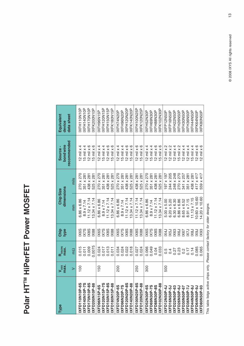
8813
.34
x 7.
1452
5 x
281
15 m
il x
6IX
TK 1
80N
15P
IXTD
50N
20P
-5S
200
75IX
5S6.
20 x
5.2
024
4 x
205
12 m
il x
3IX
TP 5
0N20
PIX
TD74
N20
P-6
S42
IX6S
6.86
x 6
.86
270
x 27
012
mil
x 4
IXTQ
74N
20P
IXTD
96N
20P
-7S
30IX
7S8.
9 x
7.14
438
x 28
115
mil
x 4
IXTQ
96N
20P
IXTD
120N
20P
-8S
28IX
8S11
.12
x 7.
1443
8 x
281
12 m
il x
6IX
TQ 1
20N
20P
4IX
TD14
0N20
P-8
824
IX88
13.3
4 x
7.14
525
x 28
115
mil
x 6
IXTK
140
N20
PIX
TD42
N25
P-5
S25
010
0IX
5S6.
20 x
5.2
024
4 x
205
12 m
il x
3IX
TP 4
2N25
PIX
TD64
N25
P-6
S60
IX6S
6.86
x 6
.86
270
x 27
012
mil
x 4
IXTQ
64N
25P
IXTD
82N
25P
-7S
40IX
7S8.
9 x
7.14
351
x 28
115
mil
x 4
IXTQ
82N
25P
IXTD
100N
25P
-8S
34IX
8S11
.12
x 7.
1443
8 x
281
12 m
il x
6IX
TQ 1
00N
25P
IXTD
120N
25P
-88
30IX
8813
.34
x 7.
1452
5 x
281
15 m
il x
6IX
TK 1
20N
25P
IXTD
36N
30P
-5S
300
135
IX5S
6.20
x 5
.20
244
x 20
512
mil
x 3
IXTP
36N
30P
IXTD
52N
30P
-6S
82IX
6S6.
86 x
6.8
627
0 x
270
12 m
il x
4IX
TQ 5
2N30
PIX
TD69
N30
P-7
S60
IX7S
8.9
x 7.
1435
1 x
281
15 m
il x
4IX
TQ 6
9N30
PIX
TD88
N30
P-8
S50
IX8S
11.1
2 x
7.14
438
x 28
112
mil
x 6
IXTQ
88N
30P
IXTD
102N
30P
-88
40IX
8813
.34
x 7.
1452
5 x
281
15 m
il x
6IX
TK 1
02N
30P
13©
200
8 IX
YS
All
right
s re
serv
ed
Type
VD
SS
RD
S(O
N)
Chi
pC
hip
Siz
eS
ourc
e -
Equ
ival
ent
max
.m
ax.
type
dim
ensi
ons
bond
wir
ede
vice
reco
mm
ende
dda
ta s
heet
Vm
Ω m
mm
ils
IXFD
110N
10P
-6S
100
0.01
5IX
6S6.
86 x
6.8
627
0 x
270
12 m
il x
4IX
FH
110N
10P
IXFD
140N
10P
-7S
0.01
1IX
7S8.
9 x
7.14
351
x 28
115
mil
x 4
IXF
H14
0N10
PIX
FD17
0N10
P-8
S0.
009
IX8S
11.1
2 x
7.14
438
x 28
112
mil
x 6
IXF
H17
0N10
PIX
FD20
0N10
P-8
80.
0075
IX88
13.3
4 x
7.14
525
x 28
115
mil
x 6
IXF
K20
0N10
PIX
FD96
N15
P-6
S15
00.
024
IX6S
6.86
x 6
.86
270
x 27
012
mil
x 4
IXF
H96
N15
PIX
FD12
0N15
P-7
S0.
017
IX7S
8.9
x 7.
1435
1 x
281
15 m
il x
4IX
FH
120N
15P
IXFD
150N
15P
-8S
0.01
3IX
8S11
.12
x 7.
1443
8 x
281
12 m
il x
6IX
FH
150N
15P
IXFD
180N
15P
-88
0.01
1IX
8813
.34
x 7.
1452
5 x
281
15 m
il x
6IX
FK
180N
15P
IXFD
74N
20P
-6S
200
0.03
4IX
6S6.
86 x
6.8
627
0 x
270
12 m
il x
4IX
FH
74N
20P
IXFD
96N
20P
-7S
0.02
4IX
7S8.
9 x
7.14
351
x 28
115
mil
x 4
IXF
H96
N20
PIX
FD12
0N20
P-8
S0.
022
IX8S
11.1
2 x
7.14
438
x 28
112
mil
x 6
IXF
H12
0N20
PIX
FD14
0N20
P-8
80.
018
IX88
13.3
4 x
7.14
525
x 28
115
mil
x 6
IXF
K14
0N20
PIX
FD10
0N25
P-8
S25
00.
027
IX8S
11.1
2 x
7.14
438
x 28
112
mil
x 6
IXF
H10
0N25
PIX
FD12
0N25
P-8
80.
024
IX88
13.3
4 x
7.14
525
x 28
115
mil
x 6
IXF
K12
0N25
PIX
FD52
N30
P-6
S30
00.
066
IX6S
6.86
x 6
.86
270
x 27
012
mil
x 4
IXF
H52
N30
PIX
FD69
N30
P-7
S0.
049
IX7S
8.9
x 7.
1435
1 x
281
15 m
il x
4IX
FH
69N
30P
IXFD
88N
30P
-8S
0.04
IX8S
11.1
2 x
7.14
438
x 28
112
mil
x 6
IXF
H88
N30
PIX
FD10
2N30
P-8
80.
033
IX88
13.3
4 x
7.14
525
x 28
115
mil
x 6
IXF
K10
2N30
PIX
FD12
N50
P-4
J50
00.
5IX
4J5.
00 x
5.0
019
7 x
197
12 m
il x
2IX
FP
12N
50P
IXFD
16N
50P
-5J
0.4
IX5J
6.20
x 5
.20
244
x 20
512
mil
x 2
IXF
P16
N50
PIX
FD22
N50
P-6
30.
27IX
636.
30 x
6.3
024
8 x
248
12 m
il x
4IX
FH
22N
50P
IXFD
26N
50P
-6J
0.23
IX6J
6.86
x 6
.86
270
x 27
015
mil
x 2
IXF
H26
N50
PIX
FD30
N50
P-6
70.
2IX
678.
65 x
6.5
234
1 x
257
12 m
il x
4IX
FH
30N
50P
IXFD
36N
50P
-7J
0.17
IX7J
8.91
x 7
.15
351
x 28
112
mil
x 4
IXF
H36
N50
PIX
FD44
N50
P-8
J0.
14IX
8J11
.13
x 7.
1543
8 x
281
15 m
il x
4IX
FH
44N
50P
IXFD
64N
50P
-9J
0.08
5IX
9J10
.60
x 10
.60
417
x 41
712
mil
x 6
IXF
K64
N50
PIX
FD80
N50
P-9
30.
065
IX93
14.2
0 x
10.6
055
9 x
417
12 m
il x
6IX
FK
80N
50P
Pol
ar H
TTM H
iPer
FET
Pow
er M
OS
FET
This
tab
le li
stgs
act
ive
chip
s on
ly.
Ple
ase
cont
act
fact
ory
for
olde
r de
sign
s.

14©
200
8 IX
YS
All
right
s re
serv
ed
Pol
ar H
VTM
HiP
erFE
T P
ower
MO
SFE
T
This
tab
le li
stgs
act
ive
chip
s on
ly.
Ple
ase
cont
act
fact
ory
for
olde
r de
sign
s.
Type
VD
SS
RD
S(O
N)
Chi
pC
hip
Siz
eS
ourc
e -
Equ
ival
ent
max
.m
ax.
type
dim
ensi
ons
bond
wir
ede
vice
reco
mm
ende
dda
ta s
heet
Vm
Ω m
mm
ils
IXFD
10N
60P
-4J
600
0.74
IX4J
5.00
x 5
.00
197
x 19
712
mil
x 2
IXF
P10
N60
PIX
FD14
N60
P-5
J0.
55IX
5J6.
20 x
5.2
024
4 x
205
12 m
il x
2IX
FH
14N
60P
IXFD
18N
60P
-63
0.4
IX63
6.30
x 6
.30
248
x 24
812
mil
x 4
IXF
H18
N60
PIX
FD22
N60
P-6
J0.
33IX
6J6.
86 x
6.8
627
0 x
270
15 m
il x
2IX
FH
22N
60P
IXFD
26N
60P
-67
0.27
IX67
8.65
x 6
.52
341
x 25
712
mil
x 4
IXF
H26
N60
PIX
FD30
N60
P-7
J0.
24IX
7J8.
91 x
7.1
535
1 x
281
12 m
il x
4IX
FH
30N
60P
IXFD
36N
60P
-8J
0.19
IX8J
11.1
3 x
7.15
438
x 28
115
mil
x 4
IXF
H36
N60
PIX
FD48
N60
P-9
J0.
14IX
9J10
.60
x 10
.60
417
x 41
712
mil
x 6
IXF
K48
N60
PIX
FD64
N60
P-9
30.
1IX
9314
.20
x 10
.60
559
x 41
712
mil
x 6
IXF
K64
N60
PIX
FD7N
80P
-4J
800
1..4
4IX
4J5.
00 x
5.0
019
7 x
197
12 m
il x
2IX
FP
7N80
PIX
FD10
N80
P-5
J1.
1IX
5J6.
20 x
5.2
024
4 x
205
12 m
il x
2IX
FP
10N
80P
IXFD
12N
80P
-63
0.85
IX63
6.30
x 6
.30
248
x 24
812
mil
x 4
IXF
H12
N80
PIX
FD14
N80
P-6
J0.
72IX
6J6.
86 x
6.8
627
0 x
270
15 m
il x
2IX
FH
14N
80P
IXFD
16N
80P
-67
0.6
IX67
8.65
x 6
.52
341
x 25
712
mil
x 4
IXF
H16
N80
PIX
FD20
N80
P-7
J0.
5IX
7J8.
90 x
7.1
435
1 x
281
12 m
il x
4IX
FH
20N
80P
IXFD
24N
80P
-8J
0.4
IX8J
11.1
2 x
7.14
438
x 28
115
mil
x 4
IXF
H24
N80
PIX
FD32
N80
P-9
J0.
27IX
9J10
.6 x
10.
641
7 x
417
12 m
il x
6IX
FN
32N
80P
IXFD
44N
80P
-93
0.19
IX93
14.2
x 1
0.6
559
x 41
712
mil
x 6
IXF
N44
N80
PIX
FD60
N80
P-9
S0.
14IX
9S15
.81
x 12
.562
2 x
492
12 m
il x
8IX
FN
60N
80P
IXFD
15N
100P
-76
1000
0.76
IX76
8.90
x 7
.14
351
x 28
115
mil
x 4
IXF
H15
N10
0PIX
FD20
N10
0P-8
50.
57IX
8512
.17
x 7.
1447
9 x
281
12 m
il x
4IX
FH
20N
100P
IXFD
26N
100P
-86
0.39
IX86
13.9
8 x
9.02
550
x 35
512
mil
x 6
IXF
K26
N10
0PIX
FD32
N10
0P-9
60.
32IX
9614
.2 x
10.
655
9 x
417
15 m
il x
6IX
FN
32N
100P
IXFD
44N
100P
-97
0.22
IX97
15.8
1 x
12.5
622
x 49
215
mil
x 6
IXF
N44
N10
0PIX
FD38
N10
0P-9
90.
21IX
9915
.81
x 14
.31
622
x 56
315
mil
x 6
IXF
N38
N10
0PIX
FD16
N12
0P-8
512
000.
95IX
8512
.17
x 7.
1447
9 x
281
12 m
il x
4IX
FH
16N
120P
IXFD
20N
120P
-86
0.57
IX86
13.9
8 x
9.02
550
x 35
512
mil
x 6
IXF
N20
N12
0PIX
FD26
N12
0P-9
60.
46IX
9614
.2 x
10.
655
9 x
417
15 m
il x
6IX
FN
26N
120P
IXFD
30N
120P
-97
0.35
IX97
15.8
1 x
12.5
622
x 49
215
mil
x 6
IXF
B30
N12
0PIX
FD32
N12
0P-9
90.
31IX
9915
.81
x 14
.31
622
x 56
315
mil
x 6
IXF
N32
N12
0P

15©
200
8 IX
YS
All
right
s re
serv
ed
Pol
arH
VTM
Pow
er M
OS
FET
This
tab
le li
stgs
act
ive
chip
s on
ly.
Ple
ase
cont
act
fact
ory
for
olde
r de
sign
s.
Type
VD
SS
RD
S(O
N)
Chi
pC
hip
Siz
eS
ourc
e -
Equ
ival
ent
max
.m
ax.
type
dim
ensi
ons
bond
wir
ede
vice
reco
mm
ende
dda
ta s
heet
VΩ
mm
mils
IXTD
1R6N
50P
-11
500
6IX
111.
91 x
1.9
175
x 7
510
mil
x 1
IXT
P1R
6N50
PIX
TD2R
4N50
P-1
J3.
5IX
1J2.
29 x
2.2
990
x 9
010
mil
x 1
IXT
P2R
4N50
PIX
TD3N
50P
-2J
2.5
IX2J
2.79
x 2
.79
110
x 11
012
mil
x 1
IXT
P3N
50P
IXTD
5N50
P-2
31.
3IX
233.
69 x
2.7
915
3 x
110
12 m
il x
1IX
TP
5N50
PIX
TD6N
50P
-3J
1IX
3J3.
60 x
3.6
014
2 x
142
15 m
il x
1IX
TP
6N50
PIX
TD8N
50P
-37
0.8
IX37
4.20
x 4
.20
165
x 16
515
mil
x 1
IXT
P8N
50P
IXTD
12N
50P
-4J
0.5
IX4J
5.00
x 5
.00
197
x 19
712
mil
x 2
IXT
P12
N50
PIX
TD16
N50
P-5
J0.
4IX
5J6.
20 x
5.2
024
4 x
205
12 m
il x
2IX
TP
16N
50P
IXTD
22N
50P
-63
0.27
IX63
6.30
x 6
.30
248
x 24
812
mil
x 4
IXT
Q22
N50
PIX
TD26
N50
P-6
J0.
23IX
6J6.
86 x
6.8
627
0 x
270
15 m
il x
2IX
TQ
26N
50P
IXTD
30N
50P
-67
0.2
IX67
8.65
x 6
.52
341
x 25
712
mil
x 4
IXT
Q30
N50
PIX
TD36
N50
P-7
J0.
17IX
7J8.
91 x
7.1
535
1 x
281
12 m
il x
4IX
TH
36N
50P
IXTD
44N
50P
-8J
0.14
IX8J
11.1
3 x
7.15
438
x 28
115
mil
x 4
IXT
Q44
N50
PIX
TD1R
4N60
P-1
160
09
IX11
1.91
x 1
.91
75 x
75
10 m
il x
1IX
TP
1R4N
60P
IXTD
2N60
P-1
J4.
7IX
1J2.
29 x
2.2
990
x 9
010
mil
x 1
IXT
P2N
60P
IXTD
3N60
P-2
J2.
8IX
2J2.
79 x
2.7
911
0 x
110
12 m
il x
1IX
TP
3N60
PIX
TD4N
60P
-23
1.9
IX23
3.69
x 2
.79
153
x 11
012
mil
x 1
IXT
P4N
60P
IXTD
5N60
P-3
J1.
6IX
3J3.
60 x
3.6
014
2 x
142
15 m
il x
1IX
TP
5N60
PIX
TD7N
60P
-37
1.1
IX37
4.20
x 4
.20
165
x 16
515
mil
x 1
IXT
P7N
60P
IXTD
10N
60P
-4J
10IX
4J5.
00 x
5.0
019
7 x
197
12 m
il x
2IX
TP
10N
60P
IXTD
14N
60P
-5J
0.55
IX5J
6.20
x 5
.20
244
x 20
512
mil
x 2
IXT
Q14
N60
PIX
TD18
N60
P-6
30.
42IX
636.
30 x
6.3
024
8 x
248
12 m
il x
4IX
TQ
18N
60P
IXTD
22N
60P
-6J
0.35
IX6J
6.86
x 6
.86
270
x 27
015
mil
x 2
IXT
Q22
N60
PIX
TD26
N60
P-6
70.
23IX
678.
65 x
6.5
234
1 x
257
12 m
il x
4IX
TH
26N
60P
IXTD
30N
60P
-7J
0.24
IX7J
8.91
x 7
.15
351
x 28
112
mil
x 4
IXT
H30
N60
PIX
TD2N
80P
-2J
800
6IX
2J2.
79 x
2.7
911
0 x
110
12 m
il x
1IX
TP
2N80
PIX
TD4N
80P
-3J
4IX
3J3.
60 x
3.6
014
2 x
142
15 m
il x
1IX
TP
4N80
PIX
TD08
N10
0P-1
A10
0020
IX1A
2.29
x 2
.29
90 x
90
10 m
il x
1IX
TP
08N
100P
IXTD
1N10
0P-1
C15
IX1C
2.54
x 2
.54
100
x 10
010
mil
x 1
IXT
P1N
100P
IXTD
1R4N
100P
-2A
11IX
2A2.
79 x
2.7
911
0 x
110
10 m
il x
1IX
TP
1R4N
100P
IXTD
2N10
0P-2
C7.
5IX
2C3.
89 x
2.7
915
3 x
110
12 m
il x
1IX
TP
2N10
0PIX
TD3N
100P
-3C
4.8
IX3C
4.39
x 3
.617
3 x
142
12 m
il x
2IX
TP
3N10
0PIX
TD06
N12
0P-1
A12
0032
IX1A
2.29
x 2
.29
90 x
90
10 m
il x
1IX
TP
06N
120P
IXTD
08N
120P
-1C
25IX
1C2.
54 x
2.5
410
0 x
100
10 m
il x
1IX
TP
08N
120P
IXTD
1N12
0P-2
A20
IX2A
2.79
x 2
.79
110
x 11
010
mil
x 1
IXT
P1N
120P
IXTD
1R4N
120P
-2C
13IX
2C3.
89 x
2.7
915
3 x
110
12 m
il x
1IX
TP
1R4N
120P
IXTD
2R4N
120P
-3C
7.5
IX3C
4.39
x 3
.617
3 x
142
12 m
il x
2IX
TP
2R4N
120P

16©
200
8 IX
YS
All
right
s re
serv
ed
N-C
hann
el D
eple
tion
Mod
e M
OS
FET
P-C
hann
el P
ower
MO
SFE
T
Dep
letio
n M
ode
MO
SFE
Ts
Dep
letio
n m
ode
MO
SFE
Ts,
unlik
e th
e re
gula
ren
hanc
emen
t typ
e M
OS
FETs
, req
uire
s a
nega
tive
gate
bia
s to
turn
it o
ff. C
onse
quen
tly th
ey r
emai
non
at o
r ab
ove
zero
gat
e bi
as v
olta
ge b
utot
herw
ise
have
sim
ilar
MO
SFE
T ch
arac
teris
tics.
Thei
r R
ds(o
n) a
nd b
reak
dow
n vo
ltage
hav
e a
posi
tive
tem
pera
ture
coe
ffici
ent,
incr
easi
ng t
hega
te b
ias
volta
ge in
crea
ses
the
gate
cha
nnel
cond
uctiv
ity a
nd s
o de
crea
ses
Rds
(on)
to
som
eex
tent
and
ther
e is
a u
sabl
e in
trins
ic d
iode
. IX
YS
Cor
pora
tion’
s IX
TP01
N10
0D is
a d
eple
tion
mod
eM
OS
FET
rate
d at
VD
SS
= 1
000
Vol
ts a
nd I D
= 1
00m
A a
nd it
s R
DS
(on)
= 1
10 O
hms
at V
GS
= 0
Vol
t. Th
eot
her
depl
etio
n m
ode
MO
SFE
T, IX
TP02
N05
D, i
sra
ted
at V
DS
S =
500
Vol
ts, I
D =
200
mA
, whi
le it
sR
DS
(on)
= 3
0 O
hms.
The
min
imum
req
uire
d ga
te b
ias
to tu
rn th
em o
ff is
–5
Vol
ts. T
hey
are
both
hou
sed
in T
O-2
20 p
acka
ge a
nd c
an d
issi
pate
25
Wat
ts a
tT C
= 2
50 C.
Ther
e ar
e m
any
appl
icat
ions
in w
hich
IXTP
01N
100D
and
IX
TP02
N05
D c
an b
e us
ed:
curr
ent
regu
lato
rs,
off-l
ine
linea
r re
gula
tors
, in
put
trans
ient
vol
tage
sup
pres
sors
, in
put
curr
ent
inru
sh
Type
VD
SS
RD
S(O
N)
Chi
pC
hip
Siz
eS
ourc
e -
Equ
ival
ent
max
.m
ax.
type
dim
ensi
ons
bond
wir
ede
vice
reco
mm
ende
dda
ta s
heet
VΩ
mm
mils
IXTD
02N
50D
-1M
500
30IX
1M1.
96 x
1.6
877
x 6
63
mil
x 1
IXT
P02
N50
DIX
TD01
N10
0D-1
M10
0011
0IX
1M1.
96 x
1.6
877
x 6
63
mil
x 1
IXT
P01
N10
0D
Type
VD
SS
RD
S(O
N)
Chi
pC
hip
Siz
eS
ourc
e -
Equ
ival
ent
max
.m
ax.
type
dim
ensi
ons
bond
wir
ede
vice
reco
mm
ende
dda
ta s
heet
VΩ
mm
mils
IXT
D36
P10
-5B
100
0.08
IX5B
6.59
x 6
.59
259
x 25
912
mil
x 3
IXT
H36
P10
IXT
D50
P10
-7B
0.06
IX7B
8.84
x 7
.18
348
x 28
315
mil
x 3
IXT
H50
P10
IXT
D16
P20
-5B
200
0.22
IX5B
6.59
x 6
.59
259
x 25
912
mil
x 3
IXT
H16
P20
IXT
D24
P20
-7B
0.16
IX7B
8.84
x 7
.18
348
x 28
315
mil
x 3
IXT
H24
P20
IXT
D8P
50-5
B50
01.
20IX
5B6.
59 x
6.5
925
9 x
259
12 m
il x
3IX
TH
7P50
IXT
D11
P50
-7B
0.75
IX7B
8.84
x 7
.18
348
x 28
315
mil
x 3
IXT
H11
P50
IXT
D10
P60
-7B
1.05
IX7B
8.84
x 7
.18
348
x 28
315
mil
x 3
IXT
H10
P60

17IXYS reserves the right to change limits, test conditions and dimensions
IX11
S
G
0.012 [0.29]
0.01
6[0
.41]
SQ
0.043 [1.10]
0.075 [1.91]
0.07
5[1
.91]
IX1M
IX1J
S
G
0.012 [0.29]
0.01
6[0
.41]
SQ
0.054 [1.38]
0.09
0[2
.29]
0.090 [2.29]
0.05
4[1
.38]
IX11
IX1J
Dimensions in inch and [mm] (1" = 25.4 mm)
IX1A IX1C
IX2A

18 © 2008 IXYS All rights reserved
G
S
IX3J
0.013 [0.34]
0.02
5[0
.63]
0.047 [1.20]
0.142 [3.60]
0.024 [0.60]
0.095 [2.40]
0.09
5[2
.40]
0.14
2[3
.60]
IX3J
Dimensions in inch and [mm] (1" = 25.4 mm)
IX2X
IX2J
S
G
0.012 [0.29]
0.01
6[0
.41]
SQ
0.020 [0.51]
0.04
8[1
.23]
0.070 [1.78]
0.07
0[1
.78]
0.11
0[2
.79]
0.110 [2.79]
IX23
SG
0.012 [0.29]
0.02
4[0
.60] 0.020 [0.50]
0.046 [1.17]
0.01
0[0
.26]
0.099 [2.52]
0.090 [2.28]
0.07
5[1
.91]
0.11
0[2
.79]
0.153 [3.89]
IX23
IX2J IX2C
IX3C

19IXYS reserves the right to change limits, test conditions and dimensions
IX45 IX4Z
IX4X
S
S
GIX4J
0.013 [0.34]
0.164 [4.17]
0.197 [5.00]
0.19
7[5
.00]
0.16
4[4
.17]
0.02
4[0
.60]
SQ
0.128 [3.26]
IX3X
Dimensions in inch and [mm] (1" = 25.4 mm)
IX4J
IX4U

20 © 2008 IXYS All rights reserved
IX5Z IX5Y
IX5U IX5S
0.244 [6.20]
IX5J
G
S
S
0.04
1[1
.03]
0.013 [0.33]0.049 [1.25]
0.031 [0.77]
0.209 [5.30]
0.01
2[0
.30]
0.16
9[4
.30]
0.20
5[5
.20]
0.046 [1.18]
Dimensions in inch and [mm] (1" = 25.4 mm)
IX5B IX5J

21IXYS reserves the right to change limits, test conditions and dimensions
IX6S
Dimensions in inch and [mm] (1" = 25.4 mm)
0.24
8[6
.30]
0.248 [6.30]
IX63
G
S
S
0.206 [5.23] SQ
0.014 [0.35]
0.032 [0.80] SQ
G S
IX62A
0.014 [0.35]
0.04
4[1
.12]
0.035 [0.88]
0.06
0[1
.51]
0.08
3[2
.10]
0.16
9[4
.30]
0.129 [3.28]
0.158 [4.01]
0.086 [2.18]
0.086 [2.19]
0.341 [8.65]
0.25
7[6
.52]
IX6J
IX62 IX63
0.27
0[6
.86]
0.270 [6.86]
G
S
S
IX6J
0.014 [0.34]
0.03
3[0
.84]
SQ
IX55 IX56

22 © 2008 IXYS All rights reserved
IX65
0.14
2[3
.60]
0.28
1[7
.15]
0.351 [8.91]
G
IX7JS
S
0.03
9[1
.00]
0.033 [0.84]
0.013 [0.34]
IX7B
0.25
7[6
.52]
0.341 [8.65]
S
S
G
IX67A
0.014 [0.35]0.
039
[1.0
0]
0.032 [0.82]
0.306 [7.78]
0.12
6[3
.19]
0.22
3[5
.65]
Dimensions in inch and [mm] (1" = 25.4 mm)
IX67
IX7J
IX7F IX7S

23IXYS reserves the right to change limits, test conditions and dimensions
Dimensions in inch and [mm] (1" = 25.4 mm)
IX72
GS
IX7Y
S S
SS
0.016 [0.41]
0.119 [3.02]0.233 [5.91]
0.350 [8.89]
0.05
0[1
.27]
0.28
2[7
.16]
0.048 [1.21]
0.11
9[3
.02]
5X0.062 [ ±1.57]± IX7Y
IX8F
0.438 [11.13]
0.28
1[7
.15]
G
IX8J S
S
0.013 [0.33]
0.04
8[1
.22]
0.048 [1.22]
0.13
2[3
.36]
IX8J
IX76 IX75

24 © 2008 IXYS All rights reserved
IX82
IX84
Dimensions in inch and [mm] (1" = 25.4 mm)
IX8S IX8X
IX8Y
IX85

25IXYS reserves the right to change limits, test conditions and dimensions
Dimensions in inch and [mm] (1" = 25.4 mm)
IX9J
G
S
S
0.014 [0.35]
0.01
4[0
.35]
0.045 [1.14]
0.04
5[1
.14]
0.417 [10.60]0.
417
[10.
60]
IX9J IX9F
IX88
IX9X IX9Y
IX86

26 © 2008 IXYS All rights reserved
Dimensions in inch and [mm] (1" = 25.4 mm)
IX93
0.559 [14.20]
0.41
7[1
0.60
]
0.013 [0.32]0.047 [1.20] SQ
0.01
3[0
.32]
0.01
6[0
.40]
0.099 [2.52]
0.115 [2.92] 0.131 [3.31] 0.134 [3.40]
0.12
4[3
.15]
0.19
3[4
.90]
G
S
S
IX93A
G
IX94
IX95
IX99
IX97

27©
200
8 IX
YS
All
right
s re
serv
ed
Rec
tifie
r Dio
des
Type
VR
RM
I RT V
JMI F(
AV)
MR
thJC
①V F
I FSM
Rev
erse
Rec
over
yV
RR
Mre
ct. d
=0.5
T VJ =
@I F
I RM
@I F
@-d
i/dt
TV
JMT
C=1
00°C
typ.
25°C
125°
C25
°C;
VR=1
00V
Vty
p. m
A°C
AK
/WV
VA
AA
AA
/µs
DW
N5
800
-0.
715
012
2.80
1.14
1.05
714
0tb
dtb
dtb
dD
WP
512
000.
712
2.80
1.14
1.05
714
0tb
dtb
dtb
dD
WN
212
00 -
0.7
122.
801.
131.
057
150
tbd
tbd
tbd
DW
N9
1800
1.0
201.
801.
301.
2630
300
tbd
tbd
tbd
DW
N17
1.5
311.
101.
361.
3550
320
tbd
tbd
tbd
DW
P17
1.5
311.
101.
391.
3750
320
tbd
tbd
tbd
DW
N21
3.0
420.
901.
351.
3380
500
tbd
tbd
tbd
DW
P21
3.0
410.
901.
371.
3680
500
tbd
tbd
tbd
DW
N35
1.5
590.
651.
251.
2080
630
1150
0.64
DW
P35
1.5
580.
651.
251.
2280
630
1150
0.64
DW
N50
2.0
780.
501.
331.
3115
090
012
501
DW
P50
2.0
760.
501.
341.
3315
090
012
501
DW
N75
2.0
115
0.33
1.27
1.23
200
1500
2450
3D
WP
752.
011
80.
351.
281.
2520
015
0024
503
DW
N11
03.
525
30.
161.
181.
1230
032
0045
506
DW
P11
03.
525
30.
161.
191.
1230
032
0045
506
DW
N34
015
.041
60.
100.
931.
0930
059
0023
530
050
DW
N10
816
00 -
3.5
253
0.16
1.19
1.12
300
3200
4550
6D
WN
347
2200
20.0
788
0.05
1.10
1.01
600
1050
027
540
050
①
Mou
nted
on
DC
B

28©
200
8 IX
YS
All
right
s re
serv
ed
Type
Chi
psD
imen
sion
sSi
-pe
rth
ickn
.W
afer
AB
mm
mm
mm
DW
N5
•11
234.
402.
100.
265
DW
P5
•11
234.
40 2
.10
0.26
5D
WN
2•
•12
042.
952.
950.
265
DW
N9
••
684
3.90
3.90
0.26
5D
WN
17•
•51
84.
454.
450.
265
DW
P17
••
518
4.45
4.45
0.26
5D
WN
21•
•34
65.
405.
400.
265
DW
P21
••
346
5.40
5.40
0.26
5D
WN
35•
•25
96.
206.
200.
265
DW
P35
••
259
6.20
6.20
0.26
5D
WN
50•
•19
87.
107.
100.
265
DW
P50
••
198
7.10
7.10
0.26
5D
WN
75•
•12
58.
708.
700.
265
DW
P75
••
125
8.70
8.70
0.26
5D
WN
110
••
5812
.30
12.3
00.
265
DW
P11
0•
•58
12.3
012
.30
0.26
5D
WN
340
•32
16.2
016
.20
0.26
5D
WN
108
••
5812
.30
12.3
00.
315
DW
N34
7•
1625
.30
18.5
00.
315
Tole
ranc
e-0
.1-0
.1±5
%
solderable
bonderable
DW
N
DW
P
Rec
tifie
r Dio
des

29©
200
8 IX
YS
All
right
s re
serv
ed
Type
VR
RM
I RT V
JMI F(
AV)
MR
thJC
①V F
I FSM
Rev
erse
Rec
over
y0.
8xV
RR
Mre
ct. d
=0.5
T VJ =
@I F
I RM
@I F
@-d
i/dt
t rr@
I F@
-di/d
t12
5°C
T C=1
00°C
typ.
25°C
@25
°C;
VR=1
00V
VR=3
0VV
mA
°CA
K/W
VV
°CA
AA
AA
/µs
nsA
A/µ
s
DW
EP
27-0
220
05.
015
054
0.9
1.09
0.84
150
3030
04
5010
035
110
0D
WE
P37
-02
11.0
910.
81.
030.
8715
010
047
54
100
100
351
200
DW
EP
77-0
220
.024
40.
40.
980.
8115
012
012
007.
510
020
0tb
d1
350
DW
EP
8-06
600
1.5
tbd
2.5
1.65
1.48
150
850
512
100
351
50D
WE
P12
-06
1.5
82.
51.
451.
3115
08
100
525
100
351
50D
WE
P15
-06
3.0
121.
61.
651.
4815
016
100
525
100
351
50D
WE
P23
-06
7.0
300.
91.
531.
3315
030
250
550
100
351
100
DW
EP
25-0
67.
030
0.9
1.53
1.38
150
4330
05
5010
035
110
0D
WE
P35
-06
14.0
600.
81.
731.
4815
070
550
510
010
035
120
0D
WE
P55
-06
17.0
800.
71.
581.
3812
575
600
510
010
035
120
0D
WE
P75
-06
20.0
162
0.4
1.31
1.12
125
7510
0020
8020
035
135
0D
WE
P3-
1010
002.
0tb
d2.
52.
652.
0915
06
407
1210
035
150
DW
EP
10-1
04.
012
1.6
2.65
2.09
150
12 7
55
2510
035
150
DW
EP
18-1
07.
030
0.9
2.43
2.04
150
3020
07
5010
035
110
0D
WE
P20
-10
7.0
300.
92.
351.
9915
036
200
750
100
351
100
DW
EP
30-1
014
.060
0.8
2.24
1.79
150
6050
07
100
100
351
200
DW
EP
50-1
017
.082
0.7
2.12
1.68
125
5050
06.
150
120
351
200
DW
EP
70-1
020
.012
90.
41.
891.
5712
575
800
1480
200
351
350
DW
EP
6-12
1200
2.0
tbd
2.5
2.55
2.19
150
580
710
100
401
50D
WE
P9-
124.
012
1.6
2.55
2.19
150
1275
525
100
501
50D
WE
P17
-12
7.0
300.
92.
602.
1915
030
200
750
100
401
100
DW
EP
19-1
27.
030
0.9
2.50
2.19
150
3020
07
5010
040
110
0D
WE
P29
-12
14.0
600.
82.
351.
9415
060
500
710
010
040
120
0D
WE
P49
-12
17.0
770.
72.
191.
8912
550
500
8.6
5010
040
120
0D
WE
P69
-12
20.0
123
0.4
1.77
1.54
125
7580
020
7520
040
135
0
①
Mou
nted
on
DC
B
FRE
D -
Fas
t Rec
over
y E
pita
xial
Dio
des

30©
200
8 IX
YS
All
right
s re
serv
ed
Type
Chi
psD
imen
sion
sSi
-pe
rth
ickn
.W
afer
AB
mm
mm
mm
DW
EP
27-0
2•
518
4.45
4.45
0.35
DW
EP
37-0
2•
257
6.20
6.20
0.35
DW
EP
77-0
2•
•15
18.
917.
220.
35D
WE
P8-
06•
1612
3.60
1.80
0.35
DW
EP
12-0
6•
•18
512.
402.
400.
35D
WE
P15
-06
••
990
3.25
3.25
0.35
DW
EP
23-0
6•
•53
15.
503.
500.
35D
WE
P25
-06
••
518
4.45
4.45
0.35
DW
EP
35-0
6•
•25
76.
206.
200.
35D
WE
P55
-06
•23
08.
654.
950.
35D
WE
P75
-06
••
151
8.91
7.22
0.35
DW
EP
3-10
•16
123.
601.
800.
35D
WE
P10
-10
•99
03.
253.
250.
35D
WE
P18
-10
•53
15.
503.
500.
35D
WE
P20
-10
•51
84.
454.
450.
35D
WE
P30
-10
••
257
6.20
6.20
0.35
DW
EP
50-1
0•
230
8.65
4.95
0.35
DW
EP
70-1
0•
151
8.91
7.22
0.35
DW
EP
6-12
•18
512.
402.
400.
35D
WE
P9-
12•
•99
03.
253.
250.
35D
WE
P17
-12
••
531
5.50
3.50
0.35
DW
EP
19-1
2•
•51
84.
454.
450.
35D
WE
P29
-12
••
257
6.20
6.20
0.35
DW
EP
49-1
2•
•23
08.
654.
950.
35D
WE
P69
-12
••
151
8.91
7.22
0.35
Tole
ranc
e-0
.1-0
.1±5
%
solderable
bonderable
FRE
D -
Fas
t Rec
over
y E
pita
xial
Dio
des

31©
200
8 IX
YS
All
right
s re
serv
ed
Type
Dim
ensi
ons
Num
ber
SiA
Bof
Chi
psth
ickn
ess
per
Waf
er
mm
mm
6 "
mm
DM
LP04
-03
•2.
12.
136
750.
25D
MLP
06-0
3•
2.4
2.4
2700
0.25
DM
LP10
-03
•3.
33.
314
300.
25D
MLP
15-0
3•
3.9
3.9
1020
0.25
DM
LP20
-03
•4.
454.
4578
00.
25D
MLP
04-0
4•
2.1
2.1
3675
0.25
DM
LP06
-04
•2.
42.
427
000.
25D
MLP
10-0
4•
3.3
3.3
1430
0.25
DM
LP15
-04
•3.
93.
910
200.
25D
MLP
20-0
4•
4.45
4.45
780
0.25
solderable
bondable
FRE
D -
Fast
Rec
over
y E
pita
xial
Dio
des
with
met
al fi
eld
plat
e
Type
VR
RM
I r R
TI R
V FV F
@ I F
rate
dI FS
MR
ever
seI F
t rrdi
/dt
Sta
tus
at 1
50°C
at R
Tat
150
°Ccu
rren
tR
ecov
ery
I RM
VuA
uAV
VA
AA
Ans
A/u
s
DM
LP04
-03
300
115
01.
250.
9510
100
310
3520
0A
vaila
ble
DM
LP06
-03
120
01.
31.
0520
150
320
3520
0A
vaila
ble
DM
LP10
-03
125
01.
280.
9530
300
330
3520
0A
vaila
ble
DM
LP15
-03
130
01.
250.
9540
400
340
3520
0A
vaila
ble
DM
LP20
-03
135
01.
280.
9560
550
360
3520
0A
vaila
ble
DM
LP04
-04
400
125
01.
351
1010
04
1045
200
Ava
ilabl
eD
MLP
06-0
41
300
1.35
1.09
1515
03.
520
4520
0A
vaila
ble
DM
LP10
-04
135
01.
351
3030
04
3045
200
Ava
ilabl
eD
MLP
15-0
41
400
1.35
140
400
440
4520
0A
vaila
ble
DM
LP20
-04
150
01.
351
6055
04
6045
200
Ava
ilabl
eD
MLP
23-0
660
0tb
dtb
dtb
dtb
d30
tbd
tbd
30tb
dtb
dD
evel
opm
ent

32©
200
8 IX
YS
All
right
s re
serv
ed
Type
VR
RM
I RT V
JMI F(
AV)
MR
thJC
①V F
I FSM
Rev
erse
Rec
over
yV
RR
Mre
ct. d
=0.5
T VJ =
@I F
I RM
@I F
@-d
i/dt
t rr@
I F@
-di/d
tT
VJM
TC=1
00°C
typ.
25°C
150°
C25
°C;
VR=1
00V
VR=3
0VV
mA
°CA
K/W
VV
AA
AA
A/µ
sty
p. n
sA
A/µ
s
DW
LP4-
0220
00.
2015
014
2.80
1.21
0.88
580
1.2
1010
025
150
DW
LP15
-02
0.50
291.
600.
990.
8212
140
2.4
2510
025
110
0D
WLP
15-0
2B0.
5025
1.60
1.13
0.84
1214
01.
125
100
251
100
DW
LP25
-02
0.20
460.
901.
100.
8530
325
2.0
5010
025
120
0D
WLP
4-03
300
0.20
132.
801.
631.
075
401.
410
100
301
50D
WLP
8-03
0.25
152.
501.
451.
016
601.
012
100
301
50D
WLP
15-0
30.
5025
1.60
1.44
1.02
1211
01.
425
100
301
100
DW
LP15
-03A
0.50
291.
601.
260.
9312
110
1.4
2510
030
110
0D
WLP
23-0
31.
0051
0.90
1.19
0.84
3030
03.
050
100
301
200
DW
LP23
-03A
1.00
410.
901.
491.
0730
300
1.9
5010
025
120
0D
WLP
55-0
32.
5072
0.65
1.42
0.99
6060
02.
813
010
030
130
0D
WLP
75-0
34.
0011
70.
401.
430.
9510
010
003.
320
010
030
140
0D
WLP
8-04
400
0.25
142.
501.
400.
976
601.
412
100
301
50D
WLP
15-0
40.
5024
1.60
1.40
0.98
1211
02.
525
100
301
100
DW
LP23
-04
1.00
460.
901.
431.
0630
300
2.5
5010
030
120
0D
WLP
55-0
42.
5067
0.65
1.38
0.99
6060
03.
513
010
030
130
0D
WLP
75-0
44.
0011
70.
401.
391.
0310
010
004.
020
010
030
140
0D
WLP
150-
048.
5014
80.
351.
381.
1230
012
009.
520
010
030
180
0D
WLP
4-06
600
0.20
112.
801.
971.
285
401.
810
100
301
50D
WLP
8-06
A0.
2512
2.50
1.75
1.22
650
2.6
1210
035
150
DW
LP8-
06B
0.25
112.
502.
341.
536
501.
412
100
301
50D
WLP
15-0
6A0.
5021
1.60
1.87
1.23
1211
02.
925
100
351
100
DW
LP15
-06B
0.50
161.
602.
381.
4412
110
1.5
2510
035
110
0D
WLP
23-0
6A1.
0040
0.90
1.54
1.17
3025
03.
550
100
351
200
DW
LP23
-06B
2.00
300.
902.
451.
5330
250
2.0
5010
030
120
0D
WLP
55-0
62.
5062
0.65
1.92
1.23
6060
04.
013
010
035
130
0D
WLP
75-0
64.
0099
0.40
1.93
1.24
100
1000
4.5
200
100
351
400
DW
LP1-
1212
000.
20tb
d25
.02.
141.
691
202.
31
100
tbd
tbd
tbd
DW
LP8-
120.
259
2.50
2.61
1.65
640
5.0
1210
040
150
DW
LP15
-12
0.50
141.
602.
451.
6812
905.
725
100
401
100
DW
LP23
-12
1.00
290.
902.
681.
7130
200
6.7
5010
040
120
0D
WLP
55-1
22.
5048
0.65
2.54
1.59
6050
07.
013
010
040
130
0D
WLP
75-1
24.
0078
0.40
2.56
1.71
100
800
7.4
200
100
401
400
①
Mou
nted
on
DC
B
Low
Lea
kage
Fas
t Rec
over
y E
pita
xial
Dio
des

33©
200
8 IX
YS
All
right
s re
serv
ed
Type
Chi
psD
imen
sion
sSi
-pe
rth
ickn
.W
afer
AB
mm
mm
mm
DW
LP4-
02•
1960
3.00
1.80
0.37
DW
LP15
-02
•99
03.
253.
250.
37D
WLP
15-0
2B•
990
3.25
3.25
0.37
DW
LP25
-02
•51
84.
454.
450.
37D
WLP
4-03
•19
603.
001.
800.
37D
WLP
8-03
•16
123.
601.
800.
37D
WLP
15-0
3•
990
3.25
3.25
0.37
DW
LP15
-03A
•99
03.
253.
250.
37D
WLP
23-0
3•
531
5.50
3.50
0.37
DW
LP23
-03A
•53
15.
503.
500.
37D
WLP
55-0
3•
•23
08.
654.
950.
37D
WLP
75-0
3•
151
8.91
7.22
0.37
DW
LP8-
04•
1612
3.60
1.80
0.38
DW
LP15
-04
•99
03.
253.
250.
38D
WLP
23-0
4•
531
5.50
3.50
0.38
DW
LP55
-04
••
230
8.65
4.95
0.38
DW
LP75
-04
••
151
8.91
7.22
0.38
DW
LP15
0-04
••
7413
.00
9.77
0.38
DW
LP4-
06•
1960
3.00
1.80
0.40
DW
LP8-
06A
•16
123.
601.
800.
40D
WLP
8-06
B•
1612
3.60
1.80
0.40
DW
LP15
-06A
•99
03.
253.
250.
40D
WLP
15-0
6B•
990
3.25
3.25
0.40
DW
LP23
-06A
•53
15.
503.
500.
40D
WLP
23-0
6B•
531
5.50
3.50
0.40
DW
LP55
-06
••
230
8.65
4.95
0.40
DW
LP75
-06
••
151
8.91
7.22
0.40
DW
LP1-
12•
•45
451.
521.
520.
46D
WLP
8-12
•16
123.
601.
800.
46D
WLP
15-1
2•
990
3.25
3.25
0.46
DW
LP23
-12
•53
15.
503.
500.
46D
WLP
55-1
2•
•23
08.
654.
950.
46D
WLP
75-1
2•
151
8.91
7.22
0.46
Tole
ranc
e-0
.1-0
.1±5
%
solderable
bonderable
Low
Lea
kage
Fas
t Rec
over
y E
pita
xial
Dio
des

34©
200
8 IX
YS
All
right
s re
serv
ed
SO
NIC
dio
des
with
gla
ss p
assi
vatio
n
Type
VR
RM
I r R
TI R
at 1
25°C
V FV F
@ I F
I FSM
Rev
erse
I Ft rr
di/d
tS
tatu
sat
RT
at 1
50°C
rate
d cu
rren
tR
ecov
ery
I RM
VuA
mA
VV
AA
AA
nsA
/us
DW
HP
0.5
slow
600
10.
12
2.22
1.2
tbd
0.25
0.5
5010
Ava
ilabl
eD
WH
P0.
51
0.1
3.5
3.55
1.2
tbd
0.2
0.5
3010
Ava
ilabl
eD
WH
P4
31
2.25
2.03
540
25
3510
0A
vaila
ble
DW
HP
105
1.5
2.38
2.14
1080
410
3520
0A
vaila
ble
DW
HP
1410
3.5
2.26
2.05
2015
08
2035
400
Ava
ilabl
eD
WH
P16
103.
52.
262.
0520
150
820
3540
0A
vaila
ble
DW
HP
2335
52.
392.
1630
200
1230
3560
0A
vaila
ble
DW
HP
56 s
low
608
1.54
1.43
6055
033
6060
1200
Ava
ilabl
eD
WH
P69
slo
w10
012
1.55
1.45
100
750
5510
060
2000
Ava
ilabl
eD
WH
P15
0 sl
ow15
020
1.55
1.45
150
1400
8215
060
3000
Ava
ilabl
eD
WH
P20
0 sl
ow25
030
1.55
1.44
250
1950
140
250
6050
00A
vaila
ble
DW
HP
5612
512
2.18
1.95
6040
024
6035
1200
Dev
elop
men
tD
WH
P69
200
202.
21.
9710
050
040
100
3520
00D
evel
opm
ent
DW
HP
150
325
302.
161.
9315
080
060
150
3530
00D
evel
opm
ent
DW
HP
200
500
452.
242.
0125
012
0010
025
035
5000
Dev
elop
men
tD
WH
P4
1200
101
2.45
2.18
535
4.2
575
150
Ava
ilabl
eD
WH
P10
51.
52.
582.
2810
658.
510
7535
0A
vaila
ble
DW
HP
1410
3.5
2.45
2.01
2013
519
2075
750
Ava
ilabl
eD
WH
P16
103.
52.
452.
220
135
1920
7575
0A
vaila
ble
DW
HP
2350
52.
592.
2930
180
2530
7510
00A
vaila
ble
DW
HP
56 s
low
608
2.04
1.76
6055
065
6065
1800
Ava
ilabl
eD
WH
P69
slo
w10
012
2.04
1.83
100
750
100
100
100
2500
Ava
ilabl
eD
WH
P15
0 sl
ow15
020
2.04
1.69
150
1400
150
150
150
4000
Ava
ilabl
eD
WH
P56
125
122.
422.
1460
430
5160
7525
00A
vaila
ble
DW
HP
6920
020
2.44
2.16
100
930
8310
075
4000
Ava
ilabl
eD
WH
P15
032
530
2.4
2.13
150
1130
115
150
125
3500
Ava
ilabl
eD
WH
P20
050
045
2.46
2.18
250
1800
170
250
125
6000
Ava
ilabl
eD
WH
P6
1600
-180
05
0.15
2.61
2.61
225
1.6
215
020
Ava
ilabl
eD
WH
P15
160.
352.
892.
8910
808.
510
150
100
Ava
ilabl
eD
WH
P25
421
2.65
2.65
2020
016
.520
150
200
Ava
ilabl
eD
WH
P55
952
2.73
2.73
4045
033
4015
040
0A
vaila
ble
DW
HP
6820
04
2.71
2.71
6065
050
6015
060
0A
vaila
ble
DW
HP
150
365
7.5
2.57
2.57
100
1100
125
150
150
1500
Ava
ilabl
eD
WH
P20
055
011
2.63
2.63
150
1600
200
250
150
2500
Ava
ilabl
eD
WH
P20
540
00-4
500
tbd
tbd
tbd
tbd
tbd
tbd
tbd
tbd
tbd
tbd
Dev
elop
men
t

35©
200
8 IX
YS
All
right
s re
serv
ed
SO
NIC
dio
des
with
gla
ss p
assi
vatio
n
Type
Dim
ensi
ons
Num
ber
SiA
Bof
Chi
psth
ickn
ess
per
Waf
er
mm
mm
mm
DW
HP
0.5-
06•
11
1077
70.
2D
WH
P4-
06•
3.6
1.8
1622
0.2
DW
HP
10-0
6•
2.95
2.95
1204
0.2
DW
HP
14-0
6•
4.8
3.3
657
0.2
DW
HP
16-0
6•
3.95
3.95
668
0.2
DW
HP
23-0
6•
5.5
3.5
532
0.2
DW
HP
56-0
6•
8.65
4.95
231
0.2
DW
HP
69-0
6•
8.91
7.22
152
0.2
DW
HP
150-
06•
11.4
9.4
880.
2D
WH
P20
0-06
•12
.412
.459
0.2
DW
HP
4-12
•3.
61.
816
220.
2D
WH
P10
-12
•2.
952.
9512
040.
2D
WH
P14
-12
•4.
83.
365
70.
2D
WH
P16
-12
•3.
953.
9566
80.
2D
WH
P23
-12
•5.
53.
553
20.
2D
WH
P56
-12
•8.
654.
9523
10.
2D
WH
P69
-12
•8.
917.
2215
20.
2D
WH
P15
0-12
•11
.49.
488
0.2
DW
HP
200-
12•
12.4
12.4
590.
2D
WH
P6-
16/1
8•
2.4
2.4
1841
0.26
5D
WH
P15
-16/
18•
3.25
3.25
988
0.26
5D
WH
P25
-16/
18•
4.45
4.45
517
0.26
5D
WH
P55
-16/
18•
8.65
4.95
231
0.26
5D
WH
P68
-16/
18•
8.91
7.22
152
0.26
5D
WH
P15
0-16
/18
•11
.49.
488
0.26
5D
WH
P20
0-16
/18
•12
.412
.459
0.26
5
DW
HP
205-
40/4
5•
14.3
14.3
450.
58•
- A
vaila
ble
on r
eque
st•
sold
er te
mpe
ratu
re b
elow
350
°C
solderable
bondable

36©
200
8 IX
YS
All
right
s re
serv
ed
GaA
s S
chot
tky
Dio
des
Type
VR
RM
T VJM
I F(A
V)M
Rth
JCV
F typ
I R ty
pC
jI FS
M
rect
. d=0
.5T V
J =@
I F@
VR
RM
0.5
• VR
RM
TC=9
0°C
typ.
25°C
125°
C12
5°C
125°
CV
°CA
K/W
VV
AµA
pFA
DW
GS
04-0
1A10
017
58.
510
.12
0.62
0.54
2.0
700
19.0
12.5
DW
GS
10-0
1C25
.05.
200.
990.
9410
.0<
1019
.080
.0D
WG
S04
-018
A18
05.
010
.12
0.86
0.85
2.0
700
8.8
12.5
DW
GS
04-0
18C
8.4
10.1
21.
251.
024.
0<
108.
832
.0D
WG
S10
-018
A11
.05.
200.
800.
805.
013
0022
.030
.0D
WG
S10
-018
C15
.05.
201.
211.
047.
5<
1022
.080
.0D
WG
S20
-018
A17
.03.
700.
800.
807.
520
0033
.050
.0D
WG
S20
-018
C23
.03.
701.
241.
0720
.0<
1033
.012
0.0
DW
GS
04-0
25A
250
3.9
10.1
21.
301.
302.
070
06.
412
.5D
WG
S04
-025
C7.
810
.12
1.26
1.05
4.0
< 10
6.4
32.0
DW
GS
10-0
25A
9.0
5.20
1.25
1.25
5.0
1300
18.0
30.0
DW
GS
10-0
25C
14.0
5.20
1.26
1.07
7.5
< 10
18.0
80.0
DW
GS
20-0
25A
13.0
3.70
1.25
1.25
7.5
2000
26.0
50.0
DW
GS
20-0
25C
20.0
3.70
1.24
1.10
20.0
< 10
26.0
120.
0D
WG
S04
-03A
300
3.5
10.1
21.
601.
602.
070
03.
712
.5D
WG
S04
-03C
6.0
10.1
21.
511.
104.
0<
103.
732
.0D
WG
S10
-03A
8.0
5.20
1.60
1.60
5.0
1300
9.0
30.0
DW
GS
10-0
3C17
.55.
201.
561.
117.
510
9.0
80.0
DW
GS
20-0
3C25
.03.
701.
561.
1420
.015
14.0
120.
0

37©
200
8 IX
YS
All
right
s re
serv
ed
SiN
Pas
siva
tion
GaA
s S
chot
tky
Dio
des
bondable
Type
Chi
psD
imen
sion
sW
afer
per
thic
knes
sW
afer
AB
mm
mm
mm
DW
GS
04-0
1A•
4060
1.30
1.30
DW
GS
10-0
1C•
2126
2.10
1.60
DW
GS
04-0
18A
•40
601.
301.
30D
WG
S04
-018
C•
4060
1.30
1.30
DW
GS
10-0
18A
•21
262.
101.
60D
WG
S10
-018
C•
2126
2.10
1.60
DW
GS
20-0
18A
•14
803.
001.
60D
WG
S20
-018
C•
1480
3.00
1.60
0.45
DW
GS
04-0
25A
•40
601.
301.
30D
WG
S04
-025
C•
4060
1.30
1.30
DW
GS
10-0
25A
•21
262.
101.
60D
WG
S10
-025
C•
2126
2.10
1.60
DW
GS
20-0
25A
•14
803.
001.
60D
WG
S20
-025
C•
1480
3.00
1.60
DW
GS
04-0
3A•
4060
1.30
1.30
DW
GS
04-0
3C•
4060
1.30
1.30
DW
GS
10-0
3A•
2126
2.10
1.60
DW
GS
10-0
3C•
2126
2.10
1.60
DW
GS
20-0
3C•
1480
3.00
1.60
Tole
ranc
e-0
.1-0
.1±1
0 %

38©
200
8 IX
YS
All
right
s re
serv
ed
Sch
ottk
y D
iode
s
Type
VR
RM
I R@
TV
JT V
JMI F
AV
MR
thJC
①V
FI F
SM
Rev
erse
Rec
over
y @
25
°CV
RR
Mre
ct. d
= 0
,5ty
p.25
°C
T VJ=
125
°C@
I FI R
Mt r
r@
I F-d
i/dt
T C =
125
°C
typ.
typ.
Vm
A°C
°CA
K/W
VV
AA
Ans
AA
/us
DW
S39
-08D
812
5010
015
014
50.
80.
310.
2160
1000
tbd
tbd
5020
0D
WS
9-15
B15
100
100
150
tbd
1.7
0.39
0.27
1016
0tb
dtb
d10
200
DW
S19
-15B
200
100
150
651.
40.
390.
2720
350
tbd
tbd
2020
0D
WS
29-1
5B35
010
015
098
1.1
0.39
0.27
4066
0tb
dtb
d40
200
DW
S7-
30B
3040
100
150
tbd
1.7
0.43
0.34
1014
0tb
dtb
d10
200
DW
S17
-30B
8010
015
0tb
d1.
40.
430.
3420
330
2.4
tbd
2020
0D
WS
217-
30B
140
100
150
651.
20.
430.
3428
420
5.5
tbd
2820
0D
WS
27-3
0B15
010
015
082
1.1
0.43
0.34
4052
0tb
dtb
d40
200
DW
S37
-30B
250
100
150
102
0.8
0.43
0.34
6080
0tb
dtb
d50
200
DW
S93
-45B
4535
100
150
tbd
tbd
0.48
0.43
7tb
dtb
dtb
d7
200
DW
S94
-45A
1.8
125
175
tbd
tbd
0.66
0.54
7tb
dtb
dtb
d7
200
DW
S3-
45B
4010
015
028
1.7
0.48
0.43
1016
0tb
dtb
d10
200
DW
S4-
45A
2.5
125
175
321.
70.
660.
5310
140
tbd
tbd
1020
0D
WS
13-4
5B10
010
015
042
1.4
0.48
0.43
2032
01.
4tb
d20
200
DW
S14
-45A
512
517
547
1.4
0.66
0.53
2028
01.
5tb
d20
200
DW
S21
3-45
B14
010
015
0tb
d1.
20.
480.
4328
tbd
tbd
tbd
2820
0D
WS
214-
45A
712
517
5tb
d1.
20.
660.
5428
tbd
tbd
tbd
2820
0D
WS
23-4
5B20
010
015
063
1.1
0.48
0.43
4064
02
tbd
4020
0D
WS
24-4
5A10
125
175
681.
10.
660.
5440
550
2tb
d40
200
DW
S33
-45B
250
100
150
890.
80.
480.
4360
900
2.6
tbd
5020
0D
WS
34-4
5A10
125
175
950.
80.
660.
5460
800
2.5
tbd
5020
0
①
Mou
nted
on
DC
B

39©
200
8 IX
YS
All
right
s re
serv
ed
Type
Chi
psD
imen
sion
sSi
per
Waf
erA
Bth
ickn
ess
6 "
mm
mm
mm
DW
S39
-08D
•51
35.
415.
410.
25D
WS
9-15
B•
2783
2.4
2.4
0.25
DW
S19
-15B
•15
023.
253.
250.
25D
WS
29-1
5B•
758
4.44
4.44
0.25
DW
S7-
30B
•27
832.
42.
40.
25D
WS
17-3
0B•
1502
3.25
3.25
0.25
DW
S21
7-30
B•
1000
4.45
3.25
0.25
DW
S27
-30B
•75
84.
444.
440.
25D
WS
37-3
0B•
513
5.41
5.41
0.25
DW
S93
-45B
•41
802
20.
25D
WS
94-4
5A•
4180
22
0.25
DW
S3-
45B
•27
832.
42.
40.
25D
WS
4-45
A•
2783
2.4
2.4
0.25
DW
S13
-45B
•15
023.
253.
250.
25D
WS
14-4
5A•
1502
3.25
3.25
0.25
DW
S21
3-45
B•
1000
4.45
3.25
0.25
DW
S21
4-45
A•
1000
4.45
3.25
0.25
DW
S23
-45B
••
758
4.44
4.44
0.25
DW
S24
-45A
•75
84.
444.
440.
25D
WS
33-4
5B•
•51
35.
415.
410.
25D
WS
34-4
5A•
•51
35.
415.
410.
25To
lera
nce
-0.1
-0.1
5%
solderable
bondable
Sch
ottk
y D
iode
s

40©
200
8 IX
YS
All
right
s re
serv
ed
Sch
ottk
y D
iode
s
Type
VR
RM
I R@
TV
JT V
JMI F
AV
MR
thJC
①V
FI F
SM
Rev
erse
Rec
over
y @
25
°CV
RR
Mre
ct. d
= 0
,5ty
p.25
°C
T VJ=
125
°C@
I FI R
Mt r
r@
I F-d
i/dt
T C =
125
°C
typ.
typ.
Vm
A°C
°CA
K/W
VV
AA
Ans
AA
/us
DW
S95
-60B
6035
100
150
tbd
tbd
0.59
0.52
7tb
dtb
dtb
d7
200
DW
S96
-60A
1.8
125
175
tbd
tbd
0.71
0.59
7tb
dtb
dtb
d7
200
DW
S5-
60B
4010
015
0tb
d1.
70.
590.
5210
170
tbd
tbd
1020
0D
WS
6-60
A2.
512
517
5tb
d1.
70.
710.
6110
170
tbd
tbd
1020
0D
WS
15-6
0B50
100
150
431.
40.
590.
5220
320
tbd
tbd
2020
0D
WS
16-6
0A5
125
175
tbd
1.4
0.71
0.59
20tb
dtb
dtb
d20
200
DW
S25
-60B
100
100
150
631.
10.
590.
5240
660
tbd
tbd
4020
0D
WS
26-6
0A10
125
175
tbd
1.1
0.71
0.59
40tb
dtb
dtb
d40
200
DW
S35
-60B
200
100
150
820.
80.
590.
4960
900
2.5
tbd
5020
0D
WS
25-8
0B80
150
100
150
661.
10.
70.
5840
660
1.5
tbd
4020
0D
WS
36-8
0A10
125
175
910.
80.
780.
6160
700
2tb
d50
200
DW
S92
-100
A10
01.
812
517
5tb
dtb
d0.
80.
637
tbd
tbd
tbd
720
0D
WS
2-10
0A2.
512
517
532
1.7
0.82
0.63
1012
02
tbd
1020
0D
WS
12-1
00A
512
517
545
1.4
0.82
0.63
2023
02.
3tb
d20
200
DW
S21
2-10
0A7
125
175
tbd
1.2
0.8
0.63
28tb
dtb
dtb
d28
200
DW
S22
-100
A10
125
175
651.
10.
820.
6340
450
2.6
tbd
4020
0D
WS
32-1
00A
2012
517
592
0.8
0.82
0.63
6070
03.
4tb
d50
200
DW
S91
-150
A15
01.
812
517
5tb
dtb
d0.
810.
667
tbd
tbd
tbd
720
0D
WS
1-15
0A2.
512
517
530
1.7
0.81
0.66
1012
03
tbd
1020
0D
WS
11-1
50A
512
517
543
1.4
0.81
0.66
2020
04
tbd
2020
0D
WS
211-
150A
712
517
5tb
d1.
20.
810.
6628
tbd
tbd
tbd
2820
0D
WS
21-1
50A
1012
517
560
1.1
0.81
0.66
4045
0tb
dtb
d40
200
DW
S31
-150
A20
125
175
850.
80.
810.
6660
700
4.5
tbd
5020
0D
WS
1-18
0A18
02.
512
517
530
1.7
0.82
0.67
1012
03.
5tb
d10
200
DW
S1-
200A
200
2.5
125
175
tbd
1.7
0.84
0.68
1012
0tb
dtb
d10
200
DW
S20
-200
A10
125
175
tbd
1.1
0.84
0.68
40tb
dtb
dtb
d40
200
DW
S30
-200
A5
125
175
tbd
0.8
0.84
0.68
6070
05
tbd
5020
0
①
Mou
nted
on
DC
B

41©
200
8 IX
YS
All
right
s re
serv
ed
Type
Chi
psD
imen
sion
sSi
per
Waf
erA
Bth
ickn
ess
mm
mm
mm
DW
S95
-60B
•41
802
20.
25D
WS
96-6
0A•
4180
22
0.25
DW
S5-
60B
•27
832.
42.
40.
25D
WS
6-60
A•
2783
2.4
2.4
0.25
DW
S15
-60B
•15
023.
253.
250.
25D
WS
16-6
0A•
1502
3.25
3.25
0.25
DW
S25
-60B
•75
84.
444.
440.
25D
WS
26-6
0A•
758
4.44
4.44
0.25
DW
S35
-60B
•51
35.
415.
410.
25D
WS
25-8
0B•
758
4.44
4.44
0.25
DW
S36
-80A
•51
35.
415.
410.
25D
WS
92-1
00A
•41
802
20.
25D
WS
2-10
0A•
2783
2.4
2.4
0.25
DW
S12
-100
A•
1502
3.25
3.25
0.25
DW
S21
2-10
0A•
1000
4.45
3.25
0.25
DW
S22
-100
A•
758
4.44
4.44
0.25
DW
S32
-100
A•
•51
35.
415.
410.
25D
WS
91-1
50A
•41
802
20.
25D
WS
1-15
0A•
2783
2.4
2.4
0.25
DW
S11
-150
A•
1502
3.25
3.25
0.25
DW
S21
1-15
0A•
1000
4.45
3.25
0.25
DW
S21
-150
A•
758
4.44
4.44
0.25
DW
S31
-150
A•
513
5.41
5.41
0.25
DW
S1-
180A
•27
832.
42.
40.
25D
WS
1-20
0A•
2783
2.4
2.4
0.25
DW
S20
-200
A•
758
4.44
4.44
0.25
DW
S30
-200
A•
513
5.41
5.41
0.25
Tole
ranc
e-0
.1-0
.15%
solderable
bondable
Sch
ottk
y D
iode
s

42©
200
8 IX
YS
All
right
s re
serv
ed
Pha
se C
ontr
ol T
hyri
stor
s
Type
VD
RM
I RT V
JMI F(
AV)
MR
thJC
②V T
I TSM
t qI H
I LV
RR
MV
RR
Mre
ct. d
=0.5
T VJ =
@I F
non-
rep.
VR =
100
V, V
D =
VD
RM
dv/d
t@
I TR
GK =
∝@
t PT V
JMT C
=100
°Cm
ax.
25°C
150°
Ct P
=10m
st P
=200
µs, d
i/dt =
-10
A/µ
sV
D =
6V
T VJ =
typ.
T VJ =
T VJM
T VJ =
25°C
25°C
Vm
A°C
AK
/WV
VA
Aµs
V/µ
sA
mA
mA
µs
CW
P7-
CG
800
-5
125
151.
71.
521.
4820
200
tbd
tbd
tbd
5075
10C
WP
812
004
150
tbd
1.7
1.50
1.46
4430
060
2016
4010
010
CW
P8-
CG
415
0tb
d1.
71.
501.
4644
300
6020
1680
100
10C
WP
3520
150
tbd
0.7
1.43
1.39
150
1050
100
1050
8010
010
CW
P16
-CG
1200
-8
150
251.
21.
371.
3345
400
150
1011
100
150
10C
WP
21-C
G16
0012
611.
11.
531.
4980
520
150
2015
100
150
10C
WP
22-C
G12
360.
91.
531.
4980
520
150
1520
100
450
10C
WP
2420
tbd
0.9
1.30
1.26
6060
060
2025
100
200
10C
WP
25-C
G20
tbd
0.9
1.24
1.20
6060
060
2025
100
200
10C
WP
4112
00 -
2012
50.
51.
501.
4620
011
5015
020
120
200
450
10C
WP
5018
0020
tbd
0.6
1.35
1.31
200
1500
150
2015
020
045
010
CW
P55
20tb
d0.
51.
261.
2220
016
0015
020
150
200
450
10C
WP
7120
tbd
0.4
1.31
1.27
300
2400
185
2015
020
045
010
CW
P13
030
204
0.2
1.19
1.15
350
4750
150
2016
020
030
030
CW
P18
040
372
0.2
1.20
1.16
450
5200
150
2030
020
030
030
CW
P34
140
tbd
0.2
1.19
1.15
600
7000
200
5030
020
020
030
CW
P34
760
540
0.1
1.15
1.11
600
9500
200
5030
015
020
030
CW
P69
1600
-20
tbd
0.2
1.52
1.48
300
1700
185
2015
015
020
030
CW
P33
922
0040
tbd
0.2
1.24
1.20
300
6000
150
2016
015
020
030
CW
P34
560
520
0.1
1.31
1.27
600
8000
200
5030
015
020
030
①
= 7
5°C
②
Mou
nted
on
DC
B
①

43©
200
8 IX
YS
All
right
s re
serv
ed
Pha
se C
ontr
ol T
hyri
stor
s
...-C
G ty
pes
solderable
bondable
Type
Chi
psD
imen
sion
sSi
-pe
rth
ickn
.W
afer
AB
FG
Cor
ner
Gat
eJ
LM
mm
mm
mm
mm
mm
mm
mm
mm
CW
P7-
CG
••
518
4.45
4.45
--
0.2
1.0
1.5
0.38
CW
P8
••
375
5.20
5.20
1.80
0.90
--
-0.
38C
WP
8-C
G•
•37
55.
205.
20-
-0.
21.
01.
50.
32C
WP
35•
•12
58.
708.
701.
801.
00-
--
0.38
CW
P16
-CG
••
239
6.50
6.50
--
0.2
1.5
1.5
0.38
CW
P21
-CG
••
196
7.10
7.10
--
0.2
1.5
1.5
0.38
CW
P22
-CG
••
196
7.10
7.10
--
0.2
1.5
1.5
0.38
CW
P24
••
196
7.10
7.10
1.80
1.00
--
-0.
32C
WP
25-C
G•
•19
67.
107.
10-
-0.
21.
51.
50.
32C
WP
41•
•94
10.0
010
.00
2.30
1.50
--
-0.
38C
WP
50•
•74
13.0
09.
772.
301.
50-
--
0.38
CW
P55
••
5812
.30
12.3
02.
301.
50-
--
0.38
CW
P71
••
5013
.40
13.4
02.
301.
50-
--
0.38
CW
P13
0•
•29
19.0
515
.40
3.46
2.50
--
-0.
38C
WP
180
••
2020
.55
17.6
53.
502.
50-
--
0.38
CW
P34
1•
1625
.30
18.5
03.
502.
50-
--
0.38
CW
P34
7•
1323
.40
23.4
03.
502.
50-
--
0.38
CW
P69
•50
13.4
013
.40
2.30
1.50
--
-0.
46C
WP
339
•16
25.3
018
.50
3.50
2.50
--
-0.
46C
WP
345
•13
23.4
023
.40
3.50
2.50
--
-0.
46To
lera
nce
-0.1
-0.1
-0.1
+0.1
-0.1
+0.1
+0.1
±5%

44©
200
8 IX
YS
All
right
s re
serv
ed
DW
FND
WFP
Fast
Rec
tifie
r Dio
des
Type
VR
RM
I RT V
JMI F(
AV)
MR
thJC
①V F
I FSM
Rev
erse
Rec
over
y0.
8xV
RR
Mre
ct. d
=0.5
T VJ =
@I F
I RM
@I F
@-d
i/dt
t rr@
I F@
-di/d
tT
VJM
T C=7
5°C
typ.
25°C
125°
C25
°Cty
p.V
typ.
mA
°CA
K/W
VV
AA
AA
A/µ
sµs
AA
/µs
DW
FN2-
16/1
816
00 -
212
510
2.9
1.79
tbd
1075
tbd
tbd
tbd
1.5
45
DW
FN9-
16/1
818
004
161.
61.
98tb
d30
160
tbd
tbd
tbd
1.5
85
DW
FN17
-16/
185
171.
31.
89tb
d55
300
tbd
tbd
tbd
1.5
1010
DW
FN21
-16/
188
230.
91.
98tb
d70
400
tbd
tbd
tbd
1.5
1515
DW
FN35
-16/
1810
260.
71.
88tb
d80
500
tbd
tbd
tbd
1.5
2525
DW
FP17
-13/
1813
00-1
800
512
517
1.3
2.10
tbd
5530
0tb
dtb
dtb
d1.
510
10D
WFP
68-1
6/18
1600
-180
05
125
480.
4tb
dtb
d70
500
45②
7025
0tb
dtb
dtb
d
①
Mou
nted
on
DC
B②
@
125
°C V
R =
100
V
Type
Chi
psD
imen
sion
sSi
per
thic
knes
s W
afer
AB
mm
mm
mm
DW
FN2-
16/1
8•
1205
2.95
2.95
0.26
5D
WFN
9-16
/18
•68
53.
903.
900.
265
DW
FN17
-16/
18•
•51
84.
454.
450.
265
DW
FN21
-16/
18•
346
5.40
5.40
0.26
5D
WFN
35-1
6/18
•26
06.
206.
200.
265
DW
FP17
-13/
18•
•51
84.
454.
450.
265
DW
FP68
-16/
18•
152
8.91
7.22
0.26
5To
lera
nce
-0.1
-0.1
±5%
solderable
bondable

45IXYS reserves the right to change limits, test conditions and dimensions
WWWWWhahahahahat is DCBt is DCBt is DCBt is DCBt is DCB
DCB stands for Direct Copper Bon-ding and denotes a process in whichcopper and a ceramic material arefused together, at high temperatures.
IXYS has developed this particularprocess in which two layers of copperare directly bonded to an aluminum-oxide or aluminum-nitride ceramicbase. Since 1981 our power moduleshave been designed with DCBsubstrates. The DCB process yields athin base and eliminates the need forthick, heavy copper bases that wereused in the past. Because moduleswith DCB bases use fewer layers, theyhave much lower thermal resistancevalues and much better power cyclingcapabilities.
Our power technology allows us toproduce DCB ceramic plates in largequantities. The dimensions of ourstandard sheet are 138 x 190.5 mm,(or 5,5“ x 7,5“).
Properties of DCB ceramicsubstrates:
• High mechanical strength andmechanically stability
• Good adhesion and corrosionresistance
• Excellent electrical insulation testedto 2.5 kV(RMS) for 1 minute or more
• Excellent thermal conductivity
• Superb thermal cycling stability
• Matched thermal expansioncoefficient to that of silicon and GaAs
• Good heat spreading
• May be etched just like PC boards
• Environmentally friendly
Advantages for the users:
• The 0.3 mm thick copper layerpermits the copper pattern to handlehigh currents.
• The excellent thermal conductivityallows the possibility to place powersemiconductor chips in very closeproximity. This results in more powerper unit of volume and improvedreliability of a power system.
• Lighter base plate material thancopper base plate.
• High voltage insulation at highertemperature.
• DCB is the basis for the „chip-on-board“ technology which is thepackaging trend for the nextgeneration integrated powermodules.
• IXYS experience in using DCB inpower modules. Wealth ofapplication know-how and support.
Starting materials for DCB ceramicsubstrates are 0.3 mm thick copper foils,shown on both sides, top and bottom of theceramic base plate.
Both sides of the finishedDCB ceramic substrate are
copper. Standard dimensionsare 138 x 190.5 mm (usable
area is 130 x 180 mm).A finished DCB part istypically nickel plated.

46 © 2008 IXYS All rights reserved
DCB DaDCB DaDCB DaDCB DaDCB Datatatatata Unclad aluminum oxide ceramic
Al2O3 content > 96 %
dimensions 138 x 190.5, 138 x 210, 115 x 165* mm
usable area max. 130 x 180, 107 x 156* mm
thickness 1.00, 0.63, 0.38, 0.25 mm
arc through voltage 10 kV
thermal conductivity > 24 W/m . K
Conduction layers - both sides
copper thickness 0.3 ±0.015 (< 0.3 on request) mm
conductor width min. 0.3 ± 0.2 mm
conductor spacing min. 0.4 ± 0.2 mm
spacing conductor/edge of ceramic min. 0.35 ± 0.2 mm
surface finishes available bare copper; nickel plated;nickel + gold plated
peel-off resistance (DIN 532282) min. 9 N/mm
DCB ceramic substrate
application temperature range -55...+850 °C
resistant to hydrogen max. up to 400 °C
thermal expansion coefficient typical 7.4 x 10⁻⁶ K-1
dimensions according
to customer specific drawing
DCB parts are available as: • bonded plate• bonded and patterned plate• prelasered, unbroken plate• individuale substrates
ALN - DCB on request
* = (for 0.25 mm thk.)
US Patent # 6,798,060 "power device and direct aluminum bonded substrate“.