Embed Size (px)
Citation preview
Research ArticlePMMA-Assisted Plasma Patterning of Graphene
AlfredoD.Bobadilla ,1,2,3,4 LeonidasE.Ocola,2AnirudhaV. Sumant,2MichaelKaminski,3
and Jorge M. Seminario 4
1Faculty of Engineering, Universidad Peruana de Ciencias Aplicadas, Surco, Lima 33, Peru2Center for Nanoscale Materials, Argonne National Laboratory, Argonne, IL 60439, USA3Nuclear Engineering Division, Argonne National Laboratory, Argonne, IL 60439, USA4Department of Chemical Engineering, Electrical and Computer Engineering, and Material Sciences and Engineering,Texas A&M University, College Station, TX 77843, USA
Correspondence should be addressed to Alfredo D. Bobadilla; [email protected] and Jorge M. Seminario; [email protected]
Received 22 April 2018; Revised 2 July 2018; Accepted 17 July 2018; Published 23 August 2018
Academic Editor: Marco Rossi
Copyright © 2018 Alfredo D. Bobadilla et al. )is is an open access article distributed under the Creative Commons AttributionLicense, which permits unrestricted use, distribution, and reproduction in any medium, provided the original work isproperly cited.
Microelectronic fabrication of Si typically involves high-temperature or high-energy processes. For instance, wafer fabrication,transistor fabrication, and silicidation are all above 500°C. Contrary to that tradition, we believe low-energy processesconstitute a better alternative to enable the industrial application of single-molecule devices based on 2Dmaterials. )e presentwork addresses the postsynthesis processing of graphene at unconventional low temperature, low energy, and low pressure inthe poly methyl-methacrylate- (PMMA-) assisted transfer of graphene to oxide wafer, in the electron-beam lithography withPMMA, and in the plasma patterning of graphene with a PMMA ribbon mask. During the exposure to the oxygen plasma,unprotected areas of graphene are converted to graphene oxide. )e exposure time required to produce the ribbon patterns ongraphene is 2 minutes. We produce graphene ribbon patterns with ∼50 nm width and integrate them into solid state and liquidgated transistor devices.
1. Introduction
Working with 2D materials such as graphene requires novelmethods to fabricate ribbon patterns. Among the traditionalmethods are a metallic or resist mask to selectively protectgraphene in plasma etch exposure [1–5] and focused ion-beam (FIB) etching [6, 7]. In an oxygen plasma at 200mTorrand 50 Watts, the etch rate of graphene is about 1 layer persecond [8], and a 5- to 10-second plasma etch exposure istypically employed to selectively etch graphene with a hy-drogen silsesquioxane (HSQ) resist [8] or metallic mask [9].At a shorter time (<4 seconds) of plasma etch exposure,graphene oxide can be generated [10]. Major drawbacks ofthe traditional methods are the lack of adaptability of FIB formass production of devices, the usage of harsh acid treat-ment to remove the HSQ resist [5] or metal mask [9, 11], andoveretching of graphene from the edges underneath themetallic ribbon mask [9]. With a HSQ ribbon mask, the
resultant width of graphene ribbon pattern is ∼10 nmsmaller than the resist mask [8]. A polymethyl-methacrylate(PMMA) resist mask can also be employed to patterngraphene, and the edge roughness of the resultant pattern is∼5 nm [3]. )e PMMA mask has been adopted in thefabrication of graphene constrictions or quantum dots[3,12–14] where they exploit the formation of “S” shapededges, which is possibly due to the strong and normallyundesired effect of etching from the edges. Despite itsadoption to fabricate quantum dots, the PMMA resist maskhas not been widely adopted to make patterns on graphene.A metallic mask is preferred instead of PMMA to makenanoscale patterns with widths or diameters smaller than50 nm [9, 11, 15].
Novel methods to fabricate ribbon patterns includemetallized DNA origami [16, 17], inorganic nanowire mask[18, 19], PMMA as sacrificial layer for a metallic mask[20, 21], and block-copolymer lithography [22, 23].
HindawiJournal of NanotechnologyVolume 2018, Article ID 8349626, 8 pageshttps://doi.org/10.1155/2018/8349626
Major drawbacks of the novel methods are the lack of controlon the creation of arbitrary patterns with block copolymer,obtaining sub-100 nm resolution with a PMMA sacri�ciallayer, and the lack of control of placement of a DNAnanostructure or nanowire on the graphene substrate.
On the other side, plasma etch exposure is also useful toreduce the number of layers in multilayer graphene down tosingle layer [24–27], to control the electronic bandgap ofgraphene by chemical functionalization [28, 29], and forcontrollably engineering atomically thin material systemswith monolayer precision [30–32].
In the present work, novel parameters for plasma pat-terning of graphene/graphene oxide are identi�ed to enablethe usage of a PMMA ribbon mask cured at low temperature(<115°C). Low-temperature curing is unconventional inelectron-beam lithography and PMMA typically shows lowresistance to oxygen plasma etching [33]. PMMA is there-fore normally considered inadequate as a mask for selectiveplasma etching at sub-50 nm resolution.
2. Materials and Methods
Graphene (Figure 1) was synthesized by chemical vapordeposition (CVD) on copper foil [34–36]. Impurities in theCVD chamber can be translated to the graphene sample, andthus, an oxygen plasma treatment of the chamber wascompleted before introducing the copper foil sample for CVDsynthesis of graphene. Brie�y, the CVD process began byannealing the copper foil at 800°C under a �ow of hydrogengas of 1000 sccm at 300Torr for 30 minutes. �en, thetemperature was set to 1000°C. When the temperature sta-bilized at 1000°C in all three monitored zones of the CVDfurnace, hydrogen gas was purged at 0.1 Torr before exposingthe copper foil to a �ow of methane of 50 sccm at 1Torr. Inthis process, graphene was deposited by the reduction ofmethane. After 3 minutes of methane �ow, the gas was purgedat 10mTorr and the furnace heater was shut o� to begin thecooling process. �e cooling process was done initially under�ows of hydrogen and argon of 1000 sccm each at 300Torr for5 minutes. For the rest of the cooling process (∼75 minutes),only the hydrogen gas was kept active. �e introduction ofargon during the initial stages (5minutes at 1000°C) of coolingyields a D peak (∼1300 cm−1) of increased intensity and a 2Dpeak (∼2650 cm−1) of reduced intensity in the Raman char-acteristics of graphene (Figure 1), which is consistent withreports of graphene with a high degree of disorder [37–39].
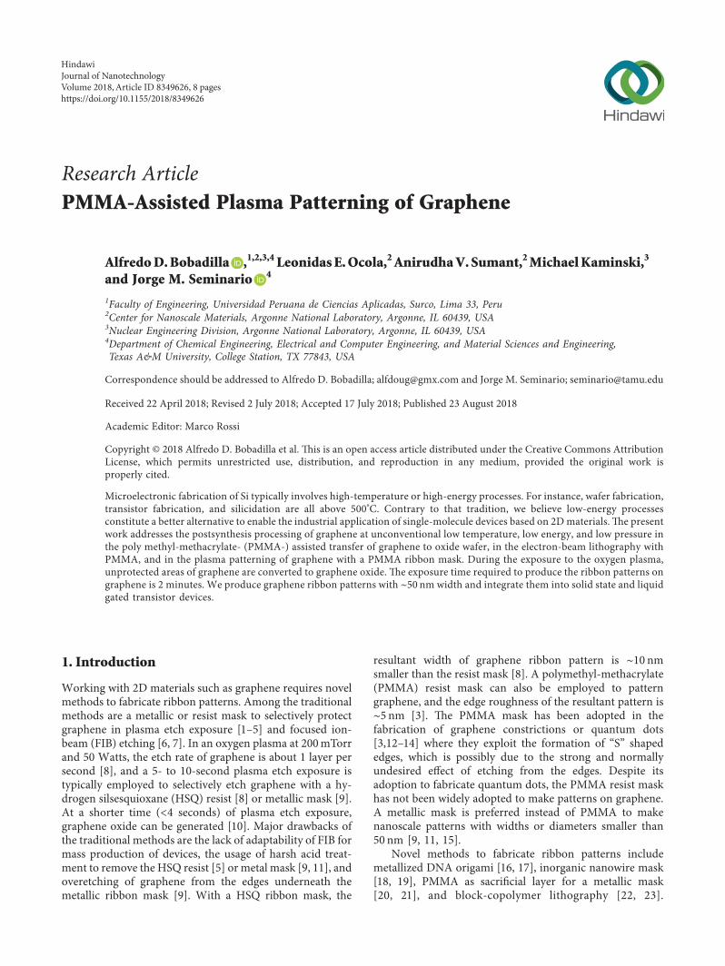
A PMMA (MicroChem) thin �lm, produced by spincoating, protected the front side of the graphene (a) duringthe etching of graphene on the backside of the copper foil ina dilute nitric acid solution (Table 1); (b) during the transferof graphene to an oxide wafer (Table 2); and (c) during theoxygen plasma patterning of graphene ribbons on silicondioxide (Figure 2).
�e curing temperature of PMMA on graphene/copperfoil and the temperature for drying of PMMA/graphene onthe oxide wafer were either room temperature (21°C) ina vented hood (∼12 hours) or 37°C on a hot plate (∼3 hours).
After the transfer of graphene from the copper foil to anoxide wafer, we need to characterize the graphene through
electrical measurements; this requires the fabrication ofa graphene ribbon with electrodes, for which four lithog-raphy steps were implemented:
(a) Patterning on top of the oxide wafer (SiO2/Si++) andbefore graphene deposition by direct-write opticallithography (Microtech LW405) of back gate elec-trodes, as interface to the highly doped silicon (Si++).
(b) Patterning of drain-source (D-S) electrodes and twoauxiliary (Aux) electrodes after graphene depositionby optical lithography. Graphene covers most of thesurface of the oxide wafer (∼1 cm2), and (D-S-Aux)electrodes were deposited on top of graphene. Backgate electrodes are employed for electrical mea-surements in air conditions. Auxiliary electrodes areemployed as gate electrodes for electrical measure-ments in aqueous conditions.
(c) Etching away by a selective exposure to oxygenplasma with a photoresist mask of the areas sur-rounding the electrodes (except the zone betweendrain and source) to avoid electrical short circuit.Graphene has a good electrical conductivity and maycause short circuits between electrodes.
(d) De�ning the ribbon pattern between drain andsource electrodes by a selective exposure to oxygenplasma with a PMMA (e-beam resist) ribbon mask.
Electrodes were based on palladium, ∼30 nm thick, anddeposited by sputtering (AJA sputtering system). S1805(MICROPOSIT S1800, �lm thickness ∼0.5 µm) was chosenas photoresist; thicker resists left more residue impurities ongraphene. �e resist was spin coated at 3000 rpm for 30seconds and cured at 90°C or 115°C for 1 minute. Acetonewas employed as a resist remover in the lifto� process. 1165solvent is the conventional remover of Shipley resists.However, we found that it causes detachment of graphenefrom the oxide substrate.
In order to perform the electron-beam (e-beam) li-thography (Raith 150 e-beam system), the PMMA resist wascured on a hot plate and we tested three temperatures: roomtemperature (21°C for 12 hours), 37°C (3 hours), and 115°C(2 minutes).We did not observe signi�cant di�erences in theoutcome of the plasma etch due to the curing temperature of
0
200
400
600
1000 1500 2000 2500 3000
Inte
nsity
(a.u
.)
Raman shift (cm–1)
Figure 1: Two typical Raman characteristic (514 nmwavelength) ofchemical vapor deposited (CVD) graphene with a high degree ofdisorder [37–39] on copper foil measured at two arbitrary points.
2 Journal of Nanotechnology
PMMA resist. IPA/water (7 : 3) was used as the developer ofPMMA [41–43] ribbon patterns at room temperature (21°C).)e optimal development time of PMMA in IPA/water wasdifferent for different curing temperatures: ∼10 s at roomtemperature, ∼15 s at 37°C, and ∼20 s at 115°C. We chosePMMA A2 950K, which originates films with ∼60 nmthickness and therefore produces PMMA nanoribbons withgood aspect ratio and stability since we need to fabricatenanoribbon patterns of width <100 nm. )e optimal de-velopment time depends on the curing temperature, thechosen optimized e-beam dose parameters, and the resultante-beam current during patterning.
Optimal parameters for the e-beam processing ofPMMA nanoribbons on graphene included a high-voltagesource of 30 kV, aperture of 10 µm, magnification of 2000,working distance of 10mm, step size of 4 nm, area dwell timeof 0.372 μs, and beam current of 34.38 pA. We test andsuggest the following doses: 80, 100, and 120 µC/cm2.
)e graphene/PMMA ribbon mask was exposed to anoxygen plasma at low pressure (<40mTorr) in a reactive ionetching (RIE) chamber (MARCH CS-1701) (Figure 2).Sometimes, there were delays of ∼5–25 seconds in the ac-tivation of the plasma at low pressure. If the delay waslonger, we turned off the plasma. Before reactivating theplasma, (a) we activated the vacuum pump to evacuate thegas; (b) set the oxygen gas pressure to 160mTorr at 20 sccm;(c) activated again the vacuum pump to evacuate the gas;and (d) set the oxygen gas pressure to 30mTorr at 1 sccm.
3. Results and Discussion
Polymer or metal masks are typically used to etch graphene.Physical vapor deposition of the metal mask inherentlyinvolves high-temperature molecular events and strongbinding of the metal to graphene. )erefore, we opted fora PMMA-based mask, a polymeric material employed ine-beam lithography as a resist. However, PMMA is wellknown to have a very low resistance to plasma oxygen [33].For example, a double layer of PMMA (PMMA 495KA2/PMMA 950K A4) can be employed to pattern a 65 nmwidth graphene ribbon [15], but a metallic mask is pre-ferred to obtain smaller ribbons with widths smaller than50 nm [9, 11, 15]. )erefore, different etch processingparameters are needed to enable PMMA as a nanoribbonmask for 50 nm or smaller widths. To find optimal pa-rameters for the effective plasma patterning of a graphenenanoribbon, we analyze the events involved in the selectiveetching process of a 2Dmaterial. During the plasma etchingprocess, at certain conditions of RF power and gas pressure,an atom of PMMA ejected at high kinetic energy canremove other PMMA atoms, this process constitutinga chain reaction. )e effect of this chain reaction on thematerial depends on the number of atoms of the materialand, therefore, will have a stronger effect in the etchingresistance of a 3D material (PMMA thin film) than in a 2Dmaterial (graphene). We suggest this is an important factorfor which PMMA can show an etching resistance to oxygenplasma as poor as that of graphene. )erefore, to findconditions of improved etching resistance for PMMA and
Table 1: Process to remove chemical vapor deposited (CVD)graphene from the backside of copper foil by floating on a dilutenitric acid solution. A polymethyl-methacrylate (PMMA) thin filmprotects the front side of graphene/copper foil.
Step Description
1Spin coating of e-beam resist (PMMA A6) on one sideof the graphene/copper foil/graphene at 3000 rpm for
1 minute
2Curing of PMMA/graphene/copper/graphene either
at 37°C for 3 hours on a hot plate or at roomtemperature (21°C) in a vented hood for 12 hours
3Etching of graphene on the backside of
PMMA/graphene/copper/graphene by floating ona solution of HNO3/H2O (1 :10) for ∼10–15 minutes
4Rinsing of PMMA/graphene/copper by floating ondistilled water for 3 minutes. Repeat three times the
procedure
5 Drying of PMMA/graphene/copper foil witha nitrogen gun
Table 2: Process to transfer the PMMA/graphene from a copperfoil to an oxide wafer. Transfer of the PMMA/graphene membranebetween recipients is made with a silicon wafer.
Step Description
1Etch copper (backside of PMMA/graphene/copper)by floating on a diluted copper etchant/H2O (1 :10)
solution for 12 hours
2 Rinse the PMMA/graphene by floating on distilledwater for 2 minutes. Repeat five times the procedure
3 Rinse the PMMA/graphene by floating on a dilutedHCl/H2O (1 : 20) solution for 15 minutes [40]
4 Rinse the PMMA/graphene by floating on distilledwater for 2 minutes. Repeat three times the procedure
5 Pick up the PMMA/graphene with an oxide (SiO2/Si)wafer
6Dry the PMMA/graphene/wafer either at 37°C for 3hours on a hot plate or at room temperature (21°C) in
a vented hood for 12 hours
O2 plasma
PMMA/graphene
/SiO2wafer
PMMA pattern
Graphene pattern
Figure 2: Patterning of graphene using a protective mask (PMMA)and exposure to oxygen plasma. Normally, PMMA shows poorresistance to oxygen plasma. )e present work proposes novelphysical processing parameters to enable the usage of PMMA asa mask to create ribbon patterns on graphene. Electron-beam(e-beam) lithography is used to create the PMMA mask.
Journal of Nanotechnology 3
for selective patterning of graphene, we should decreasethe energy and the number of oxygen ions that initiate thechain reaction. Our aim was to find the lowest power, thelowest oxygen pressure, and the shortest time needed toetch graphene.
Firstly, we explored much lower levels of power to testthe plasma etch resistance of graphene. We hypothesizedthat the strength of adhesion of graphene to the substrate caninfluence the etch resistance of graphene. We do not reportthe influence of different values of temperature (duringgraphene transfer or resist curing) on the resistance ofgraphene to plasma etching. However, we found that bakingdry graphene/SiO2 at 150°C or 180°C makes it significantlymore difficult to remove graphene by exposure to oxygenplasma, so that higher power (>50 Watts) is needed to etchgraphene. Working with temperature levels lower than115°C at all stages of the fabrication process, graphene hasa lower strength of adhesion to the oxide wafer and is easierto etch.
We found that 8 Watts is the minimum level of powerneeded to effectively pattern graphene in a reproducible way;at this level of power, our graphene sample on 300 nm thickSiO2 becomes optically transparent after ∼2 minutes ofplasma exposure (oxygen, 20 sccm, 160mTorr).
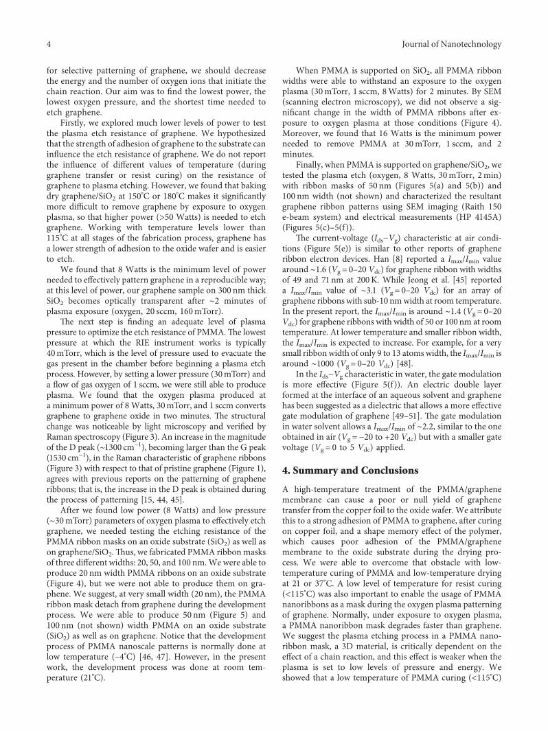
)e next step is finding an adequate level of plasmapressure to optimize the etch resistance of PMMA.)e lowestpressure at which the RIE instrument works is typically40mTorr, which is the level of pressure used to evacuate thegas present in the chamber before beginning a plasma etchprocess. However, by setting a lower pressure (30mTorr) anda flow of gas oxygen of 1 sccm, we were still able to produceplasma. We found that the oxygen plasma produced ata minimum power of 8 Watts, 30mTorr, and 1 sccm convertsgraphene to graphene oxide in two minutes. )e structuralchange was noticeable by light microscopy and verified byRaman spectroscopy (Figure 3). An increase in the magnitudeof the D peak (∼1300 cm−1), becoming larger than the G peak(1530 cm−1), in the Raman characteristic of graphene ribbons(Figure 3) with respect to that of pristine graphene (Figure 1),agrees with previous reports on the patterning of grapheneribbons; that is, the increase in the D peak is obtained duringthe process of patterning [15, 44, 45].
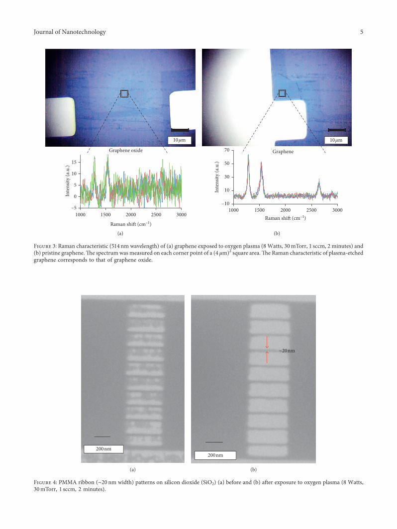
After we found low power (8 Watts) and low pressure(∼30mTorr) parameters of oxygen plasma to effectively etchgraphene, we needed testing the etching resistance of thePMMA ribbon masks on an oxide substrate (SiO2) as well ason graphene/SiO2.)us, we fabricated PMMA ribbonmasksof three different widths: 20, 50, and 100 nm.We were able toproduce 20 nm width PMMA ribbons on an oxide substrate(Figure 4), but we were not able to produce them on gra-phene. We suggest, at very small width (20 nm), the PMMAribbon mask detach from graphene during the developmentprocess. We were able to produce 50 nm (Figure 5) and100 nm (not shown) width PMMA on an oxide substrate(SiO2) as well as on graphene. Notice that the developmentprocess of PMMA nanoscale patterns is normally done atlow temperature (–4°C) [46, 47]. However, in the presentwork, the development process was done at room tem-perature (21°C).
When PMMA is supported on SiO2, all PMMA ribbonwidths were able to withstand an exposure to the oxygenplasma (30mTorr, 1 sccm, 8Watts) for 2 minutes. By SEM(scanning electron microscopy), we did not observe a sig-nificant change in the width of PMMA ribbons after ex-posure to oxygen plasma at those conditions (Figure 4).Moreover, we found that 16 Watts is the minimum powerneeded to remove PMMA at 30mTorr, 1 sccm, and 2minutes.
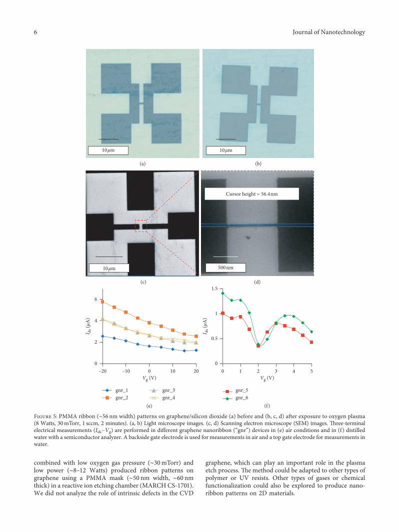
Finally, when PMMA is supported on graphene/SiO2, wetested the plasma etch (oxygen, 8 Watts, 30mTorr, 2min)with ribbon masks of 50 nm (Figures 5(a) and 5(b)) and100 nm width (not shown) and characterized the resultantgraphene ribbon patterns using SEM imaging (Raith 150e-beam system) and electrical measurements (HP 4145A)(Figures 5(c)–5(f)).
)e current-voltage (Ids−Vg) characteristic at air condi-tions (Figure 5(e)) is similar to other reports of grapheneribbon electron devices. Han [8] reported a Imax/Imin valuearound ∼1.6 (Vg� 0–20 Vdc) for graphene ribbon with widthsof 49 and 71 nm at 200K. While Jeong et al. [45] reporteda Imax/Imin value of ∼3.1 (Vg� 0–20 Vdc) for an array ofgraphene ribbons with sub-10 nmwidth at room temperature.In the present report, the Imax/Imin is around ∼1.4 (Vg� 0–20Vdc) for graphene ribbons with width of 50 or 100 nm at roomtemperature. At lower temperature and smaller ribbon width,the Imax/Imin is expected to increase. For example, for a verysmall ribbonwidth of only 9 to 13 atomswidth, the Imax/Imin isaround ∼1000 (Vg� 0–20 Vdc) [48].
In the Ids−Vg characteristic in water, the gate modulationis more effective (Figure 5(f )). An electric double layerformed at the interface of an aqueous solvent and graphenehas been suggested as a dielectric that allows a more effectivegate modulation of graphene [49–51]. )e gate modulationin water solvent allows a Imax/Imin of ∼2.2, similar to the oneobtained in air (Vg �−20 to +20 Vdc) but with a smaller gatevoltage (Vg � 0 to 5 Vdc) applied.
4. Summary and Conclusions
A high-temperature treatment of the PMMA/graphenemembrane can cause a poor or null yield of graphenetransfer from the copper foil to the oxide wafer. We attributethis to a strong adhesion of PMMA to graphene, after curingon copper foil, and a shape memory effect of the polymer,which causes poor adhesion of the PMMA/graphenemembrane to the oxide substrate during the drying pro-cess. We were able to overcome that obstacle with low-temperature curing of PMMA and low-temperature dryingat 21 or 37°C. A low level of temperature for resist curing(<115°C) was also important to enable the usage of PMMAnanoribbons as a mask during the oxygen plasma patterningof graphene. Normally, under exposure to oxygen plasma,a PMMA nanoribbon mask degrades faster than graphene.We suggest the plasma etching process in a PMMA nano-ribbon mask, a 3D material, is critically dependent on theeffect of a chain reaction, and this effect is weaker when theplasma is set to low levels of pressure and energy. Weshowed that a low temperature of PMMA curing (<115°C)
4 Journal of Nanotechnology
10µm
–5
0
5
10
15
1000 1500 2000 2500 3000
Inte
nsity
(a.u
.)
Raman shift (cm–1)
Graphene oxide
(a)
10µm
Graphene
–10
10
30
50
70
1000 1500 2000 2500 3000In
tens
ity (a
.u.)
Raman shift (cm–1)
(b)
Figure 3: Raman characteristic (514 nm wavelength) of (a) graphene exposed to oxygen plasma (8 Watts, 30mTorr, 1 sccm, 2 minutes) and(b) pristine graphene.�e spectrumwasmeasured on each corner point of a (4 µm)2 square area.�e Raman characteristic of plasma-etchedgraphene corresponds to that of graphene oxide.
200nm
(a)
~20nm
200nm
(b)
Figure 4: PMMA ribbon (∼20 nm width) patterns on silicon dioxide (SiO2) (a) before and (b) after exposure to oxygen plasma (8 Watts,30mTorr, 1 sccm, 2 minutes).
Journal of Nanotechnology 5
combined with low oxygen gas pressure (∼30mTorr) andlow power (∼8–12 Watts) produced ribbon patterns ongraphene using a PMMA mask (∼50 nm width, ∼60 nmthick) in a reactive ion etching chamber (MARCHCS-1701).We did not analyze the role of intrinsic defects in the CVD
graphene, which can play an important role in the plasmaetch process. �e method could be adapted to other types ofpolymer or UV resists. Other types of gases or chemicalfunctionalization could also be explored to produce nano-ribbon patterns on 2D materials.
10µm
(a)
10µm
(b)
10µm
(c)
0
2
4
6
–20 –10 0 10 20
I ds (µA
)
Vg (V)
gnr_1 gnr_3gnr_2 gnr_4
(e)
0
0.5
1
1.5
0 1 2 3 4 5
I ds (µA
)
Vg (V)
gnr_5gnr_6
(f)
Cursor height = 56.4nm
500nm
(d)
Figure 5: PMMA ribbon (∼56 nm width) patterns on graphene/silicon dioxide (a) before and (b, c, d) after exposure to oxygen plasma(8 Watts, 30mTorr, 1 sccm, 2 minutes). (a, b) Light microscope images. (c, d) Scanning electron microscope (SEM) images. �ree-terminalelectrical measurements (Ids−Vg) are performed in di�erent graphene nanoribbon (“gnr”) devices in (e) air conditions and in (f) distilledwater with a semiconductor analyzer. A backside gate electrode is used for measurements in air and a top gate electrode for measurements inwater.
6 Journal of Nanotechnology
Data Availability
)e data used to support the findings of this study are in-cluded within the article.
Disclosure
)e submitted manuscript has been created by UChicagoArgonne, LLC, Operator of Argonne National Laboratory(“Argonne”). Argonne, a U.S. Department of Energy Officeof Science laboratory, is operated under Contract DE-AC02-06CH11357. )e U.S. Government retains for itself, andothers acting on its behalf, a paid-up nonexclusive, irrev-ocable worldwide license in said article to reproduce, pre-pare derivative works, distribute copies to the public, andperform publicly and display publicly, by or on behalf of thegovernment.
Conflicts of Interest
)e authors declare no conflicts of interest exist.
Acknowledgments
)e Center for Nanoscale Materials was supported by theU.S. Department of Energy, Office of Science, Office of BasicEnergy Sciences, under Contract DE-AC02-06CH11357.)e authors also acknowledge financial support fromArgonne National Laboratory’s Laboratory-Directed Re-search and Development Strategic Initiative.
References
[1] S. Kumar, N. Peltekis, K. Lee, H.-Y. Kim, and G. S. Duesberg,“Reliable processing of graphene using metal etchmasks,”Nanoscale Research Letters, vol. 6, no. 1, p. 390, 2011.
[2] C. Lian, K. Tahy, T. Fang, G. Li, H. G. Xing, and D. Jena,“Quantum transport in graphene nanoribbons patterned bymetal masks,” Applied Physics Letters, vol. 96, no. 10, article103109, 2010.
[3] L. Ponomarenko, F. Schedin, M. Katsnelson et al., “ChaoticDirac billiard in graphene quantum dots,” Science, vol. 320,no. 5874, pp. 356–358, 2008.
[4] Z. Chen, Y.-M. Lin, M. J. Rooks, and P. Avouris, “Graphenenano-ribbon electronics,” Physica E: Low-Dimensional Sys-tems and Nanostructures, vol. 40, no. 2, pp. 228–232, 2007.
[5] M. Y. Han, B. Ozyilmaz, Y. Zhang, and P. Kim, “Energy band-gap engineering of graphene nanoribbons,” Physical ReviewLetters, vol. 98, no. 20, article 206805, 2007.
[6] Z. Ye, H. Chao, S. Rujie et al., “A large-area 15 nm graphenenanoribbon array patterned by a focused ion beam,” Nano-technology, vol. 25, no. 13, article 135301, 2014.
[7] M. C. Lemme, D. C. Bell, J. R. Williams et al., “Etching ofgraphene devices with a helium ion beam,” ACS Nano, vol. 3,no. 9, pp. 2674–2676, 2009.
[8] M. Y. Han, Electronic transport in graphene nanoribbons, Ph.D. doctoral dissertation, Physics, Columbia University, NewYork, NY, USA, 2010.
[9] A. Behnam, A. S. Lyons, M.-H. Bae et al., “Transport innanoribbon interconnects obtained from graphene grown bychemical vapor deposition,” Nano Letters, vol. 12, no. 9,pp. 4424–4430, 2012.
[10] I. Childres, L. A. Jauregui, J. Tian, and Y. P. Chen, “Effect ofoxygen plasma etching on graphene studied using Ramanspectroscopy and electronic transport measurements,” NewJournal of Physics, vol. 13, no. 2, article 025008, 2011.
[11] A. El Fatimy, R. L. Myers-Ward, A. K. Boyd, K. M. Daniels,D. K. Gaskill, and P. Barbara, “Epitaxial graphene quantumdots for high-performance terahertz bolometers,” NatureNanotechnology, vol. 11, no. 4, pp. 335–338, 2016.
[12] L.-J. Wang, G.-P. Guo, D. Wei et al., “Gates controlledparallel-coupled double quantum dot on both single layer andbilayer graphene,” Applied Physics Letters, vol. 99, no. 11,article 112117, 2011.
[13] D. Wei, H.-O. Li, G. Cao et al., “Tuning inter-dot tunnelcoupling of an etched graphene double quantum dot byadjacent metal gates,” Scientific Reports, vol. 3, no. 1, p. 3175,2013.
[14] X.-X. Song, H.-O. Li, J. You et al., “Suspending effect on low-frequency charge noise in graphene quantum dot,” ScientificReports, vol. 5, no. 1, p. 8142, 2015.
[15] M.-H. Bae, Z. Li, Z. Aksamija et al., “Ballistic to diffusivecrossover of heat flow in graphene ribbons,” Nature Com-munications, vol. 4, no. 1, p. 1734, 2013.
[16] Z. Jin, W. Sun, Y. Ke et al., “Metallized DNA nanolithographyfor encoding and transferring spatial information for gra-phene patterning,” Nature Communications, vol. 4, no. 1,p. 1663, 2013.
[17] J. Choi, H. Chen, F. Li et al., “Nanomanufacturing of 2Dtransition metal dichalcogenide materials using self-assembled DNA nanotubes,” Small, vol. 11, no. 41,pp. 5520–5527, 2015.
[18] J. Bai, X. Duan, and Y. Huang, “Rational fabrication ofgraphene nanoribbons using a nanowire etch mask,” NanoLetters, vol. 9, no. 5, pp. 2083–2087, 2009.
[19] A. Sinitskii and J. M. Tour, “Patterning graphene nanoribbonsusing copper oxide nanowires,” Applied Physics Letters,vol. 100, no. 10, article 103106, 2012.
[20] N. Kang, C. W. Smith, M. Ishigami, and S. I. Khondaker,“Simple patterning of large-area graphene by metal mask andsacrificial polymer layer,” ECS Meeting Abstracts,vol. MA2014-01, p. 1262, 2014.
[21] T. Kaplas, A. Bera, A. Matikainen, P. Paakkonen, andH. Lipsanen, “Transfer and patterning of chemical vapordeposited graphene by a multifunctional polymer film,”Applied Physics Letters, vol. 112, no. 7, article 073107, 2018.
[22] J. G. Son, M. Son, K.-J. Moon et al., “Sub-10 nm graphenenanoribbon array field-effect transistors fabricated by blockcopolymer lithography,” Advanced Materials, vol. 25, no. 34,pp. 4723–4728, 2013.
[23] H. S. Suh, D. H. Kim, P. Moni et al., “Sub-10-nm patterningvia directed self-assembly of block copolymer films witha vapour-phase deposited topcoat,” Nature Nanotechnology,vol. 12, no. 6, pp. 575–581, 2017.
[24] K. S. Hazra, J. Rafiee, M. A. Rafiee et al., “)inning ofmultilayer graphene to monolayer graphene in a plasmaenvironment,” Nanotechnology, vol. 22, no. 2, article 025704,2011.
[25] H. Al-Mumen, F. Rao, W. Li, and L. Dong, “Singular sheetetching of graphene with oxygen plasma,” Nano-Micro Let-ters, vol. 6, no. 2, pp. 116–124, 2014.
[26] K. S. Kim, Y. J. Ji, Y. Nam et al., “Atomic layer etching ofgraphene through controlled ion beam for graphene-basedelectronics,” Scientific Reports, vol. 7, no. 1, p. 2462, 2017.
[27] A. Davydova, E. Despiau-Pujo, G. Cunge, and D. B. Graves,“H+ ion-induced damage and etching of multilayer graphene
Journal of Nanotechnology 7
in H2 plasmas,” Journal of Applied Physics, vol. 121, no. 13,article 133301, 2017.
[28] R. Balog, B. Jorgensen, L. Nilsson et al., “Bandgap opening ingraphene induced by patterned hydrogen adsorption,”NatureMaterials, vol. 9, no. 4, pp. 315–319, 2010.
[29] A. Felten, A. Eckmann, J. J. Pireaux, R. Krupke, andC. Casiraghi, “Controlled modification of mono- and bilayergraphene in O2, H2 and CF4 plasmas,” Nanotechnology,vol. 24, no. 35, article 355705, 2013.
[30] G. Lee, J. Kim, K. Kim, and J. W. Han, “Precise control ofdefects in graphene using oxygen plasma,” Journal of VacuumScience & Technology A, vol. 33, article 060602, 2015.
[31] A. V. Jagtiani, H. Miyazoe, J. Chang et al., “Initial evaluationand comparison of plasma damage to atomic layer carbonmaterials using conventional and low Te plasma sources,”Journal of Vacuum Science & Technology A, vol. 34, article01B103, 2016.
[32] S. G. Walton, S. C. Hernandez, D. R. Boris, T. B. Petrova, andG. M. Petrov, “Electron beam generated plasmas for theprocessing of graphene,” Journal of Physics D: Applied Physics,vol. 50, no. 35, article 354001, 2017.
[33] D. J. Carbaugh, S. G. Pandya, J. T. Wright, S. Kaya, andF. Rahman, “Enhancing the dry etch resistance of polymethylmethacrylate patterned with electron beam lithography,”Journal of Vacuum Science & Technology B, vol. 35, article041602, 2017.
[34] R. Gulotty, S. Das, Y. Liu, and A. V. Sumant, “Effect of hy-drogen flow during cooling phase to achieve uniform andrepeatable growth of bilayer graphene on copper foils overlarge area,” Carbon, vol. 77, pp. 341–350, 2014.
[35] I. Vlassiouk, M. Regmi, P. Fulvio et al., “Role of hydrogen inchemical vapor deposition growth of large single-crystalgraphene,” ACS Nano, vol. 5, no. 7, pp. 6069–6076, 2011.
[36] Z. R. Robinson, P. Tyagi, T. R. Mowll, C. A. Ventrice, andJ. B. Hannon, “Argon-assisted growth of epitaxial grapheneon Cu (111),” Physical Review B, vol. 86, no. 23, article 235413,2012.
[37] E. H. Martins Ferreira, M. V. O. Moutinho, F. Stavale et al.,“Evolution of the Raman spectra from single-, few-, andmany-layer graphene with increasing disorder,” PhysicalReview B, vol. 82, no. 12, article 125429, 2010.
[38] S. Claramunt, A. Varea, D. Lopez-Dıaz, M. M. Velazquez,A. Cornet, and A. Cirera, “)e importance of interbands onthe interpretation of the Raman spectrum of graphene oxide,”Journal of Physical Chemistry C, vol. 119, no. 18, pp. 10123–10129, 2015.
[39] A. Eckmann, A. Felten, A. Mishchenko et al., “Probing thenature of defects in graphene by Raman spectroscopy,” NanoLetters, vol. 12, no. 8, pp. 3925–3930, 2012.
[40] X. Liang, B. A. Sperling, I. Calizo et al., “Toward clean andcrackless transfer of graphene,” ACS Nano, vol. 5, no. 11,pp. 9144–9153, 2011.
[41] L. E. Ocola, “Development characteristics of PMMA in al-ternative alcohol:water mixtures,” in Proceedings of the APSMarch Meeting, San Antonio, TX, USA, March 2015.
[42] S. Yasin, D. G. Hasko, and H. Ahmed, “Comparison of MIBK/IPA and water/IPA as PMMA developers for electron beamnanolithography,” Microelectronic Engineering, vol. 61-62,pp. 745–753, 2002.
[43] S. Yasin, D. G. Hasko, and H. Ahmed, “Fabrication of <5 nmwidth lines in poly(methylmethacrylate) resist using a water:isopropyl alcohol developer and ultrasonically-assisted de-velopment,” Applied Physics Letters, vol. 78, no. 18,pp. 2760–2762, 2001.
[44] A. Lyons, “Properties of graphene nanoribbons obtained bychemical vapor deposition,” M.Sc., Electrical and ComputerEngineering, University of Illinois at Urbana-Champaign,Champaign, IL, USA, 2012.
[45] S.-J. Jeong, S. Jo, J. Lee et al., “Self-aligned multichannelgraphene nanoribbon transistor arrays fabricated at waferscale,” Nano Letters, vol. 16, no. 9, pp. 5378–5385, 2016.
[46] L. E. Ocola and A. Stein, “Effect of cold development onimprovement in electron-beam nanopatterning resolutionand line roughness,” Journal of Vacuum Science & TechnologyB: Microelectronics and Nanometer Structures, vol. 24, no. 6,pp. 3061–3065, 2006.
[47] B. Cord, J. Lutkenhaus, and K. K. Berggren, “Optimal tem-perature for development of poly(methylmethacrylate),”Journal of Vacuum Science & Technology B: Microelectronicsand Nanometer Structures, vol. 25, no. 6, pp. 2013–2016, 2007.
[48] J. P. Llinas, A. Fairbrother, G. B. Barin et al., “Short-channelfield-effect transistors with 9-atom and 13-atom wide gra-phene nanoribbons,” Nature Communications, vol. 8, no. 1,p. 633, 2017.
[49] J. Xia, F. Chen, J. Li, and N. Tao, “Measurement of thequantum capacitance of graphene,” Nature Nanotechnology,vol. 4, no. 8, pp. 505–509, 2009.
[50] C. Reiner-Rozman, M. Larisika, C. Nowak, and W. Knoll,“Graphene-based liquid-gated field effect transistor for bio-sensing: )eory and experiments,” Biosensors and Bio-electronics, vol. 70, pp. 21–27, 2015.
[51] A. D. Bobadilla, L. E. Ocola, A. V. Sumant, M. Kaminski,N. Kumar, and J. M. Seminario, “Europium effect on theelectron transport in graphene ribbons,” Journal of PhysicalChemistry C, vol. 119, no. 39, pp. 22486–22495, 2015.
8 Journal of Nanotechnology

CorrosionInternational Journal of
Hindawiwww.hindawi.com Volume 2018
Advances in
Materials Science and EngineeringHindawiwww.hindawi.com Volume 2018
Hindawiwww.hindawi.com Volume 2018
Journal of
Chemistry
Analytical ChemistryInternational Journal of
Hindawiwww.hindawi.com Volume 2018
Scienti�caHindawiwww.hindawi.com Volume 2018
Polymer ScienceInternational Journal of
Hindawiwww.hindawi.com Volume 2018
Hindawiwww.hindawi.com Volume 2018
Advances in Condensed Matter Physics
Hindawiwww.hindawi.com Volume 2018
International Journal of
BiomaterialsHindawiwww.hindawi.com
Journal ofEngineeringVolume 2018
Applied ChemistryJournal of
Hindawiwww.hindawi.com Volume 2018
NanotechnologyHindawiwww.hindawi.com Volume 2018
Journal of
Hindawiwww.hindawi.com Volume 2018
High Energy PhysicsAdvances in
Hindawi Publishing Corporation http://www.hindawi.com Volume 2013Hindawiwww.hindawi.com
The Scientific World Journal
Volume 2018
TribologyAdvances in
Hindawiwww.hindawi.com Volume 2018
Hindawiwww.hindawi.com Volume 2018
ChemistryAdvances in
Hindawiwww.hindawi.com Volume 2018
Advances inPhysical Chemistry
Hindawiwww.hindawi.com Volume 2018
BioMed Research InternationalMaterials
Journal of
Hindawiwww.hindawi.com Volume 2018
Na
nom
ate
ria
ls
Hindawiwww.hindawi.com Volume 2018
Journal ofNanomaterials
Submit your manuscripts atwww.hindawi.com