Embed Size (px)
Citation preview

310
This article can be downloaded from http://www.ijerst.com/currentissue.php
Int. J. Engg. Res. & Sci. & Tech. 2015 Kavitha Chenna Reddy et al., 2015
ZSI-DVR ELIMINATION OF SHOOT THROUGHPROBLEMS AND DEEP SAG COMPENSATION
WITH HFL CONTROLLER
The growth in the use of power electronics has caused a greater awareness of power quality.Voltage sags, swells, harmonics can cause equipment to fail, mis-operate or shut down, as wellas create huge current imbalances which could blow fuses or trip breakers. These effects canbe very expensive for the customer, ranging from minor quality variations to production downtimeand equipment damage. The Dynamic Voltage Restorer (DVR) is fast, flexible and efficientsolution to voltage sag/swell problem. In this work Z-Source Inverter (ZSI) based DVR will beproposed. The ZSI uses an LC impedance grid to couple power source to inverter circuit andprepares the possibility of voltage buck and boost by short circuiting the inverter legs. ZSI basedDVR is controlled by PI controller. PI control scheme suffers from fixed gains, i.e., it cannotadapt itself to the varying parameter and conditions of system. To overcome this drawback thiswork proposes a fuzzy controller. This is a non linear controller and it can provide a betterperformance under changing system parameters and operating conditions based on knowledgebase and rule base. This work proposes another control method of Hybrid fuzzy-PI which iscombination of PI and fuzzy controllers. The control schemes of ZSI based DVR are modelledand simulated in MATLAB/SIMULINK under voltage sags and swells.
Keywords: Power quality, Dynamic Voltage Restorer (DVR), Voltage sag/swell, Z-SourceInverter (ZSI), Pulse Width Modulation (PWM), Fuzzy, Hybrid fuzzy
INTRODUCTIONTHE voltage sag/swell is the most common powerquality related problem among the industries.Such voltage sag/swell have a major impact onthe performance of the microprocessor based1 Assistant Professor, Department of Electrical & Electronics Engineering, New Horizon College of Engineering, Bangalore, Karnataka,
India.
Int. J. Engg. Res. & Sci. & Tech. 2015
ISSN 2319-5991 www.ijerst.comVol. 4, No. 4, November 2015
© 2015 IJERST. All Rights Reserved
Research Paper
loads as well as the sensitive loads. In a powerline voltage sags/swells can occur as a result ofload switching, motor starting, faults, lightning,non-linear loads, intermittent loads, Voltage sags/swells as shown in Table 1 and within which
Kavitha Chenna Reddy1*, D Satish Kumar1 and Geetanjali Pawanekar1
*Corresponding Author: Kavitha Chenna Reddy [email protected]

311
This article can be downloaded from http://www.ijerst.com/currentissue.php
Int. J. Engg. Res. & Sci. & Tech. 2015 Kavitha Chenna Reddy et al., 2015
controlling equipment should be connectedtogether with the critical loads as correctivemeasures [1]. DVR is a commercially availablecost effective device, which is capable ofaddressing the above voltage sag problemeffectively.
Apart from non-linear loads, some systemevents, both usual (capacitor switching, motorstarting) and unusual (faults) could also inflictpower quality problems. The consequence ofpower quality problems could range from a simplenuisance flicker in electric lamps to a loss ofthousand of rupees due to power shutdown. Apower quality problem is defined as anymanifested problem in voltage or current ofleading to frequency deviations that result in failureor miss operation of customer equipment.
Power quality problems associated with anextensive number of electromagnetic phenomenain power systems with broad ranges of timeframes such as long duration variations, shortduration variations and other disturbances. Shortduration variations are mainly caused by eitherfault conditions or energisation distance relatedto impedance type of grounding and connectionof transformer between the faulted location andnode, there can be temporary load of voltagereduction (sag) or voltage rise (swell) at differentnodes of the system.
Here the control scheme used employed in Z-source inverter based DVR is fuzzy controller.
The most common choice controller of the DVRis the PI controller since it has simple structureand it can offer relatively satisfactory performanceover a wide range of operation. But by using fixedgains, the controller may not provide the requiredcontrol performance, when there are variationsin the system parameters and operatingconditions. It appears that the non linearcontrollers are more suitable than the linear typesince the DVR is truly a non linear system. Theproposed fuzzy controller will provide the desiredinjecting voltage.
The Z-source converter employs a unique X-shaped impedance network on its dc side forachieving both voltagebuck and boost capabilitiesthis unique features that cannot be obtained inthe traditional voltage-source and current-sourceconverters. The proposed system is able tocompensate long and significantly large voltagesags [2], [5] and [9].
DYNAMIC VOLTAGERESTORERThe DVR employs IGBT solid-state power-electronic switching devices in a Pulse-WidthModulated (PWM) inverter structure and iscapable of generating or absorbing independently-controllable real and reactive power at its acpower-frequency transformer. So, the transformersize, weight and stress factor is reducedconsiderably [3]. Output terminal. Its dc inputterminal is connected to an energy source or anenergy storage device of appropriatecapacity.
The DVR is a solid-state dc to ac switchingpower converter that injects a set of three-phaseac output voltage in series and synchronism withthe distribution feeder voltages. The amplitude andphase angle of the injected voltages are variablethereby allowing control of the real and reactive
Table 1: Definitions for Voltage Sagand Swell
312
This article can be downloaded from http://www.ijerst.com/currentissue.php
Int. J. Engg. Res. & Sci. & Tech. 2015 Kavitha Chenna Reddy et al., 2015
power exchange between the DVR and thedistribution system within predetermined positive(power supply) and negative (power absorption)limits. The PWM main inverter structure withinthe prototype portable trailer enclosure. Thereactive power exchanged between the DVR andthe distribution system is internally generated bythe DVR without any ac passive reactivecomponents, e.g., reactors or capacitors. Realpower exchanged at the DVR ac terminals mustbe provided at the DVR dc terminal by an externalenergy source or energy storage system.
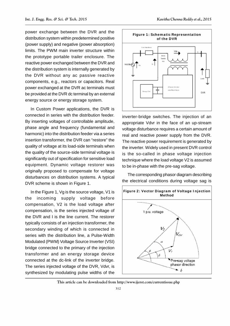
In Custom Power applications, the DVR isconnected in series with the distribution feeder.By inserting voltages of controllable amplitude,phase angle and frequency (fundamental andharmonic) into the distribution feeder via a seriesinsertion transformer, the DVR can “restore” thequality of voltage at its load-side terminals whenthe quality of the source-side terminal voltage issignificantly out of specification for sensitive loadequipment. Dynamic voltage restorer wasoriginally proposed to compensate for voltagedisturbances on distribution systems. A typicalDVR scheme is shown in Figure 1.
In the Figure 1, Vg is the source voltage, V1 isthe incoming supply voltage beforecompensation, V2 is the load voltage aftercompensation, is the series injected voltage ofthe DVR and I is the line current. The restorertypically consists of an injection transformer, thesecondary winding of which is connected inseries with the distribution line, a Pulse-WidthModulated (PWM) Voltage Source Inverter (VSI)bridge connected to the primary of the injectiontransformer and an energy storage deviceconnected at the dc-link of the inverter bridge.The series injected voltage of the DVR, Vdvr, issynthesized by modulating pulse widths of the
inverter-bridge switches. The injection of anappropriate Vdvr in the face of an up-streamvoltage disturbance requires a certain amount ofreal and reactive power supply from the DVR.The reactive power requirement is generated bythe inverter. Widely used in present DVR controlis the so-called in phase voltage injectiontechnique where the load voltage V2 is assumedto be in-phase with the pre-sag voltage.
The corresponding phasor diagram describingthe electrical conditions during voltage sag is
Figure 1: Schematic Representationof the DVR
Figure 2: Vector Diagram of Voltage InjectionMethod

313
This article can be downloaded from http://www.ijerst.com/currentissue.php
Int. J. Engg. Res. & Sci. & Tech. 2015 Kavitha Chenna Reddy et al., 2015
depicted, where only the affected phase is shownfor clarity. Let the voltage quantities Il, , and represent the load current, load power factorangle, supply voltage phase angle and loadvoltage advance angle respectively. Althoughthere is a phase advancement of á in the loadvoltage with respect to the pre-sag voltage inFigure 2, only in-phase compensation where theinjected voltage is in phase with the supply voltage( = ) is considered.
Z-SOURCE INVERTERZ-source inverter has X-shaped impedancenetwork on its DC side, which interfaces thesource and inverter H-bridge. It facilitates bothvoltage-buck and boost capabilities. Theimpedance network composed of split inductorsand two capacitors. The supply can be DC voltagesource or DC current source or AC source. Z-source inverter can be of current source type orvoltage source type. Figure 3 shows the generalblock diagram of Z-Source inverter voltage.
required conversion. A stream of pulse widthmodulation is produced to control the switch asshown in the Figure 4.
As shown in Table 2, the single-phase Z-Source inverter has five switching modes. Twoactive modes in which the dc source, voltage isapplied to load, two zero modes in which theinverter’s output terminals are short circuited byS1 and S3 or S2 and S4 switches and a shoot-through mode which occurs as two switches ona single leg are turned on.
Applying a distinctive PWM method isnecessary for ZSI considering the definedoperational modes. In a symmetric impedancenetwork, the following equations are valid:
Figure 3: General Block Diagram of Z-SourceInverter
Z-Source inverter operation is controlled bymultiple pulse width modulation. The output of theZ-Source inverter is controlled by using pulsewidth modulation, generated by comparing atriangular wave signal with an adjustable DCreference and hence the duty cycle of theswitching pulse could be varied to synthesize the
Figure 4: Multiple Pulse Width Modulation
Table 2: Switching Modes
314
This article can be downloaded from http://www.ijerst.com/currentissue.php
Int. J. Engg. Res. & Sci. & Tech. 2015 Kavitha Chenna Reddy et al., 2015
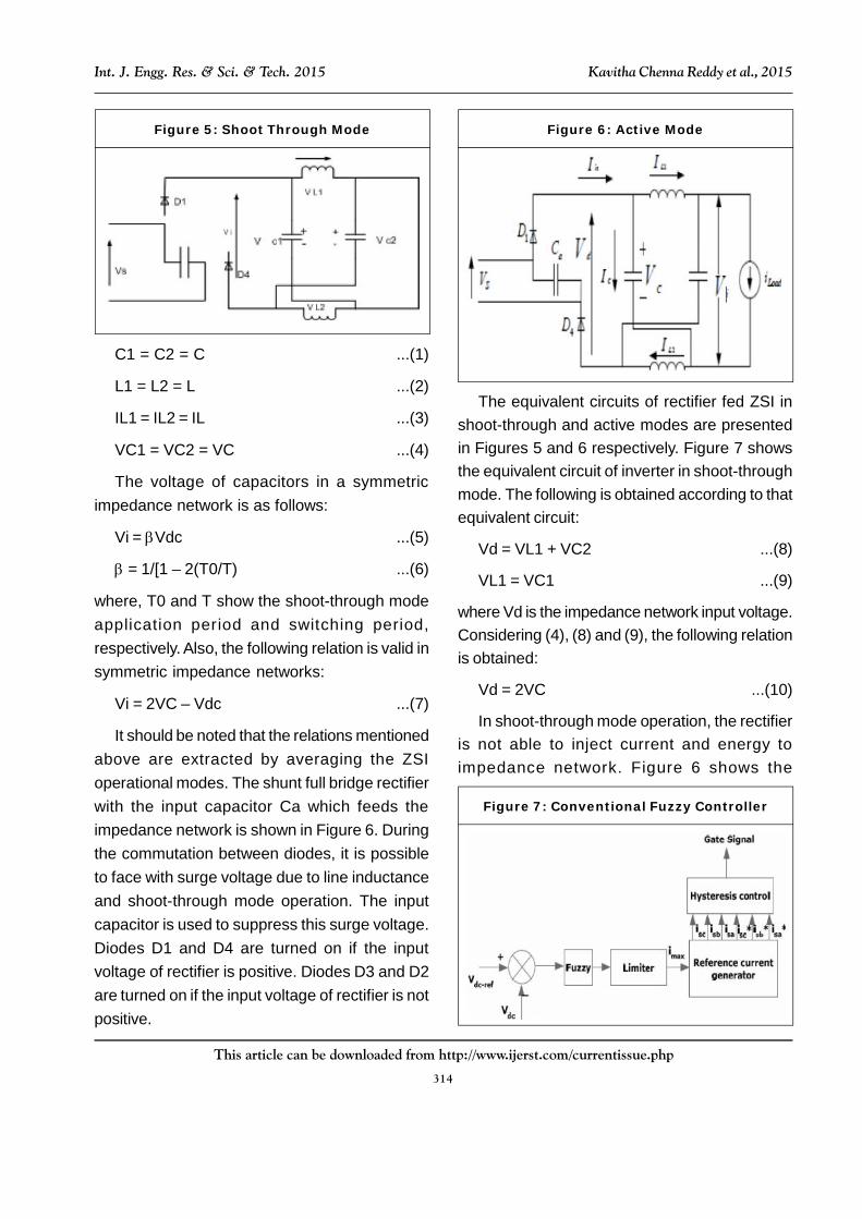
The equivalent circuits of rectifier fed ZSI inshoot-through and active modes are presentedin Figures 5 and 6 respectively. Figure 7 showsthe equivalent circuit of inverter in shoot-throughmode. The following is obtained according to thatequivalent circuit:
Vd = VL1 + VC2 ...(8)
VL1 = VC1 ...(9)
where Vd is the impedance network input voltage.Considering (4), (8) and (9), the following relationis obtained:
Vd = 2VC ...(10)
In shoot-through mode operation, the rectifieris not able to inject current and energy toimpedance network. Figure 6 shows the
C1 = C2 = C ...(1)
L1 = L2 = L ...(2)
IL1 = IL2 = IL ...(3)
VC1 = VC2 = VC ...(4)
The voltage of capacitors in a symmetricimpedance network is as follows:
Vi = Vdc ...(5)
= 1/[1 – 2(T0/T) ...(6)
where, T0 and T show the shoot-through modeapplication period and switching period,respectively. Also, the following relation is valid insymmetric impedance networks:
Vi = 2VC – Vdc ...(7)
It should be noted that the relations mentionedabove are extracted by averaging the ZSIoperational modes. The shunt full bridge rectifierwith the input capacitor Ca which feeds theimpedance network is shown in Figure 6. Duringthe commutation between diodes, it is possibleto face with surge voltage due to line inductanceand shoot-through mode operation. The inputcapacitor is used to suppress this surge voltage.Diodes D1 and D4 are turned on if the inputvoltage of rectifier is positive. Diodes D3 and D2are turned on if the input voltage of rectifier is notpositive.
Figure 5: Shoot Through Mode Figure 6: Active Mode
Figure 7: Conventional Fuzzy Controller

315
This article can be downloaded from http://www.ijerst.com/currentissue.php
Int. J. Engg. Res. & Sci. & Tech. 2015 Kavitha Chenna Reddy et al., 2015
equivalent circuit of ZSI in active mode.Considering Figure 6, the following relation isobtained,
Vd = Vs(t) – 2Vg ...(11)
CONSTRUCTION OF FUZZYCONTROLLERFigure 7 shows the internal structure of the controlcircuit. The control scheme consists of Fuzzycontroller, limiter, and three phase sine wavegenerator for reference current generation andgeneration of switching signals. The peak valueof reference currents is estimated by regulatingthe DC link voltage. The actual capacitor voltageis compared with a set reference value. The errorsignal is then processed through a Fuzzycontroller, which contributes to zero steady errorin tracking the reference current signal.
A fuzzy controller converts a linguistic controlstrategy into an automatic control strategy, andfuzzy rules are constructed by expert experienceor knowledge database. Firstly, input voltage Vdc
and the input reference voltage Vdc-ref have beenplaced of the angular velocity to be the inputvariables of the fuzzy logic controller. Then theoutput variable of the fuzzy logic controller ispresented by the control Current Imax. To convertthese numerical variables into linguistic variables,the following seven fuzzy levels or sets arechosen as: NB (negative big), NM (negativemedium), NS (negative small), ZE (zero), PS(positive small), PM (positive medium), and PB(positive big) as shown in Figure 8.
The fuzzy controller is characterized asfollows:
• Seven fuzzy sets for each input and output;
• Fuzzification using continuous universe of dis-course;
• Implication using Mamdani’s ‘min’ operator;
• De-fuzzification using the ‘centroid’ method.
Fuzzification: The process of converting anumerical variable (real number) convert to alinguistic variable (fuzzy number) is calledfuzzification.
De-fuzzification: The rules of FLC generaterequired output in a linguistic variable (FuzzyNumber), according to real world requirements,linguistic variables have to be transformed to crispoutput (Real number).
Database: The Database stores the definition ofthe membership Function required by fuzzifier anddefuzzifier.
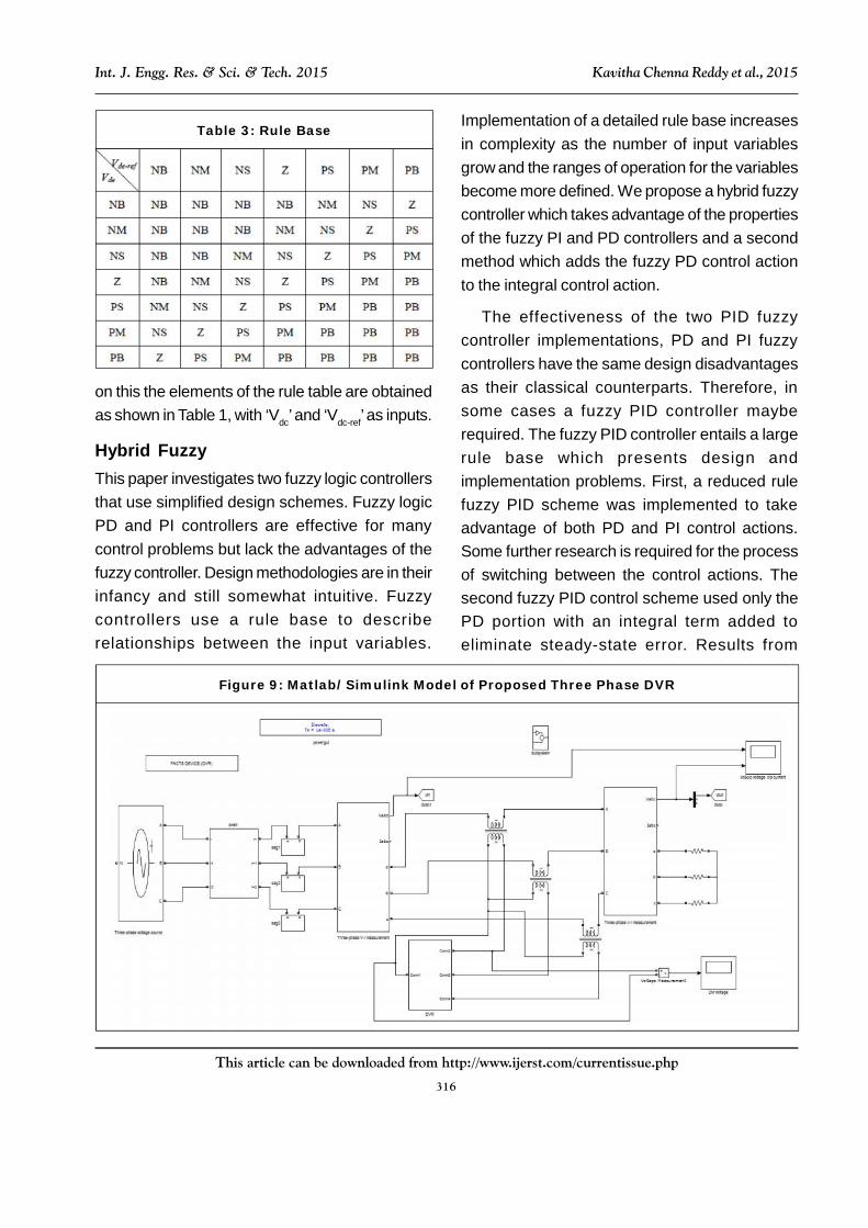
Rule Base: The elements of this rule base tableare determined based on the theory that in thetransient state, large errors need coarse control,which requires coarse in-put/output variables; inthe steady state, small errors need fine control,which requires fine input/output variables. Based
Figure 8: (a) Input Vdc NormalizedMembership Function; (b) Input Vdc-Ref
Normalized Membership Function; (c) OutputImax Normalized Membership Function
316
This article can be downloaded from http://www.ijerst.com/currentissue.php
Int. J. Engg. Res. & Sci. & Tech. 2015 Kavitha Chenna Reddy et al., 2015
on this the elements of the rule table are obtainedas shown in Table 1, with ‘Vdc’ and ‘Vdc-ref’ as inputs.
Hybrid FuzzyThis paper investigates two fuzzy logic controllersthat use simplified design schemes. Fuzzy logicPD and PI controllers are effective for manycontrol problems but lack the advantages of thefuzzy controller. Design methodologies are in theirinfancy and still somewhat intuitive. Fuzzycontrollers use a rule base to describerelationships between the input variables.
Implementation of a detailed rule base increasesin complexity as the number of input variablesgrow and the ranges of operation for the variablesbecome more defined. We propose a hybrid fuzzycontroller which takes advantage of the propertiesof the fuzzy PI and PD controllers and a secondmethod which adds the fuzzy PD control actionto the integral control action.
The effectiveness of the two PID fuzzycontroller implementations, PD and PI fuzzycontrollers have the same design disadvantagesas their classical counterparts. Therefore, insome cases a fuzzy PID controller mayberequired. The fuzzy PID controller entails a largerule base which presents design andimplementation problems. First, a reduced rulefuzzy PID scheme was implemented to takeadvantage of both PD and PI control actions.Some further research is required for the processof switching between the control actions. Thesecond fuzzy PID control scheme used only thePD portion with an integral term added toeliminate steady-state error. Results from
Table 3: Rule Base
Figure 9: Matlab/Simulink Model of Proposed Three Phase DVR
317
This article can be downloaded from http://www.ijerst.com/currentissue.php
Int. J. Engg. Res. & Sci. & Tech. 2015 Kavitha Chenna Reddy et al., 2015
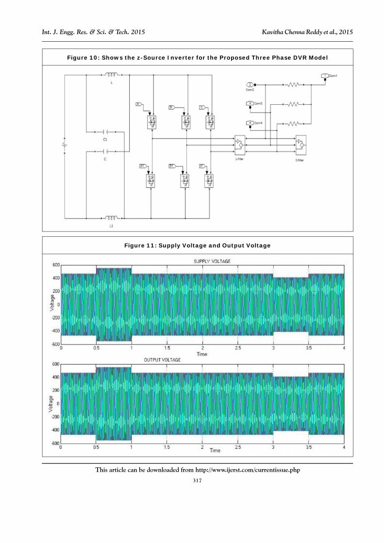
Figure 11: Supply Voltage and Output Voltage
Figure 10: Shows the z-Source Inverter for the Proposed Three Phase DVR Model

318
This article can be downloaded from http://www.ijerst.com/currentissue.php
Int. J. Engg. Res. & Sci. & Tech. 2015 Kavitha Chenna Reddy et al., 2015
simulations of both control schemes demonstratethe effectiveness of the PID controllers.
MATLAB MODELEING ANDSIMULATION RESULTSCompensation of Three Phase VoltageSag and Voltage Swell Using DVR
Figure shows the Matlab/Simulink Model ofProposed Three Phase DVR using Matlab/Simulink Platform.
Figure shows the Supply and Output Voltageswithout DVR, both voltage sag and swell problemin output voltage.
Figure 12: Matlab/Simulink Model of PI Controller for DVR
Figure 13: Simulated Output Wave Forms of Output Voltage and Supply Voltagewith PI Controlled DVR
319
This article can be downloaded from http://www.ijerst.com/currentissue.php
Int. J. Engg. Res. & Sci. & Tech. 2015 Kavitha Chenna Reddy et al., 2015
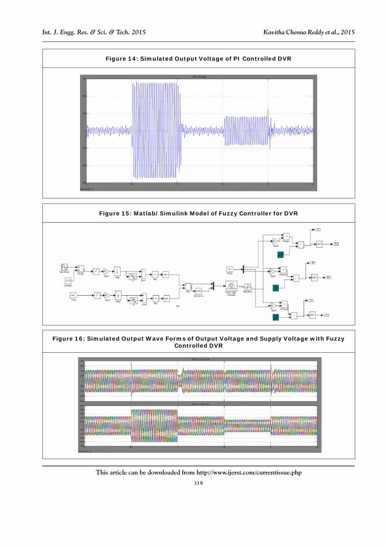
Figure 14: Simulated Output Voltage of PI Controlled DVR
Figure 15: Matlab/Simulink Model of Fuzzy Controller for DVR
Figure 16: Simulated Output Wave Forms of Output Voltage and Supply Voltage with FuzzyControlled DVR

320
This article can be downloaded from http://www.ijerst.com/currentissue.php
Int. J. Engg. Res. & Sci. & Tech. 2015 Kavitha Chenna Reddy et al., 2015
carried out using MATLAB/SIMULINK software.The simulation results shows that theperformance of Z – source inverter based DVRalong with Hybrid fuzzy controller is bettercompared to PI and fuzzy controller.
REFERENCES1. Choi S S, Li B H and Vilathgamuwa D M
(2000), “Dynamic Voltage Restoration withMinimum Energy Injection”, IEEE Trans.Power Systems, Vol. 15, pp. 51-57.
2. Gajanayake C J, Vilathgamuwa D M and Loh
Figure 17: Matlab/Simulink Model of Hybrid Fuzzy Controller for DVR
CONCLUSIONThe Dynamic Voltage Restorer (DVR) is fast,flexible and efficient solution to voltage sag/swellproblem. In this work Z-source inverter (ZSI)based DVR will be proposed. DVR serves as aneffective custom power device for mitigatingvoltage sag/swell in the distribution system. In thispaper Z– source inverter based DVR along withh fuzzy controller is modeled and the same isinstalled in the distribution system to providerequired load side compensation. The simulationof the DVR along with the proposed controller is
Figure 18: Simulated Output Wave Forms of Output Voltage and Supply Voltage with FuzzyControlled DVR
321
This article can be downloaded from http://www.ijerst.com/currentissue.php
Int. J. Engg. Res. & Sci. & Tech. 2015 Kavitha Chenna Reddy et al., 2015
P C (2005), “Smallsignal and Signal-Flow-Graph Modeling of Switched Z-sourceImpedance Network”, IEEE PowerElectronics Letters, Vol. 3, pp. 111-116.
3. Jain S K, Agrawala P and Gupta H O (2002),“Fuzzy Logic Controlled Shuntactive Filterfor Power Quality Improvement”, IEEEProceedings of EPS., Vol. 149, No. 7,pp. 317-328.
4. Jimichi T, Fujita H and Akagi H (2005),“Design and Experimentation of a DynamicVoltage Restorer Capable of SignificantlyReducing an Energystorage Element”, inConf. Record Industry ApplicationsConference, 14th IAS Annual Meeting.
5. Loh P C, Vilathgamuwa D M, Lai Y S, ChuaG T and Li Y (2004), “Pulse-Width Modulationof Z-source Inverters”, in Conf. Record IEEEIndustry Applications Conference, 39th IASAnnual Meeting.
6. Peng F Z (2003), “Z-source Inverter”, IEEETrans. Industry Applications, Vol. 39,pp. 504-510.
7. Samra N A, Neft C, Sundaram A and MalcolmW (1995), “The Distribution SystemDynamic Voltage Restorer and itsApplications at Industrial Facilities withSensitive Loads”, in Proc. Power ConversionIntell. Motion Power Quality Long Beach, CA.
8. Singh G K, Singh A K and Maitra R (2007),“A Simple Fuzzy Logic Basedrobust AcivePower Filter for Harmonics Minimization
Under Random Loadvariation”, EPSR,Vol. 77, 8, pp. 1101-1111, Elsevier Publ.
9. Sira-Ramirez H and Ortega R (1995),“Passivity-Based Controllers for theStabilization of DC-to-DC PowerConverters”, in Proc. 34th IEEE Conferenceon Decision and Control.
10. Sng E K K, Choi S S and Vilathgamuwa D M(2004), “Analysis of Series Compensationand DC-Link Voltage Controls of aTransformerless Selfcharging DynamicVoltage Restorer”, IEEE Trans. PowerDelivery, Vol. 19, pp. 1511-1518.
11. Thenmozhi C E, Gopinath C and RameshR (2012), “A Novel Method for Voltage Sag/Swell Compensation Using Dynamic VoltageRestorer”, IEEE Trans., March, 978-81-909042-2-3.
12. Torabzad S, Babaei E and Kalantari M (2010),“Z-Source Inverter Based Dynamic VoltageRestorer”, 1st Power Electronic & DriveSystems & Technologies Conference.
13. Voltage Sag/Swell Compensation Using Z-source Inverter DVR Based on FUZZYController, 2013 IEEE InternationalConference on Emerging Trends inComputing, Communication andNanotechnology (ICECCN 2013), 978-1-4673-5036-5/13/$31.00 © 2013 IEEE
14. Woodley N H, Morgan L and Sundaram A(1999), “Experience with an Inverter-BasedDynamic Voltage Restorer”, IEEE Trans.Power Delivery, Vol. 14, pp. 1181-1186.